US7091130B1 - Method of forming a nanocluster charge storage device - Google Patents
Method of forming a nanocluster charge storage deviceDownload PDFInfo
- Publication number
- US7091130B1 US7091130B1US10/876,820US87682004AUS7091130B1US 7091130 B1US7091130 B1US 7091130B1US 87682004 AUS87682004 AUS 87682004AUS 7091130 B1US7091130 B1US 7091130B1
- Authority
- US
- United States
- Prior art keywords
- layer
- forming
- material layer
- gate
- overlying
- Prior art date
- Legal status (The legal status is an assumption and is not a legal conclusion. Google has not performed a legal analysis and makes no representation as to the accuracy of the status listed.)
- Expired - Lifetime, expires
Links
Images


Classifications
- H—ELECTRICITY
- H10—SEMICONDUCTOR DEVICES; ELECTRIC SOLID-STATE DEVICES NOT OTHERWISE PROVIDED FOR
- H10B—ELECTRONIC MEMORY DEVICES
- H10B41/00—Electrically erasable-and-programmable ROM [EEPROM] devices comprising floating gates
- H10B41/40—Electrically erasable-and-programmable ROM [EEPROM] devices comprising floating gates characterised by the peripheral circuit region
- H10B41/42—Simultaneous manufacture of periphery and memory cells
- H10B41/49—Simultaneous manufacture of periphery and memory cells comprising different types of peripheral transistor
- B—PERFORMING OPERATIONS; TRANSPORTING
- B82—NANOTECHNOLOGY
- B82Y—SPECIFIC USES OR APPLICATIONS OF NANOSTRUCTURES; MEASUREMENT OR ANALYSIS OF NANOSTRUCTURES; MANUFACTURE OR TREATMENT OF NANOSTRUCTURES
- B82Y10/00—Nanotechnology for information processing, storage or transmission, e.g. quantum computing or single electron logic
- H—ELECTRICITY
- H10—SEMICONDUCTOR DEVICES; ELECTRIC SOLID-STATE DEVICES NOT OTHERWISE PROVIDED FOR
- H10B—ELECTRONIC MEMORY DEVICES
- H10B41/00—Electrically erasable-and-programmable ROM [EEPROM] devices comprising floating gates
- H10B41/40—Electrically erasable-and-programmable ROM [EEPROM] devices comprising floating gates characterised by the peripheral circuit region
- H—ELECTRICITY
- H10—SEMICONDUCTOR DEVICES; ELECTRIC SOLID-STATE DEVICES NOT OTHERWISE PROVIDED FOR
- H10B—ELECTRONIC MEMORY DEVICES
- H10B43/00—EEPROM devices comprising charge-trapping gate insulators
- H10B43/30—EEPROM devices comprising charge-trapping gate insulators characterised by the memory core region
- H—ELECTRICITY
- H10—SEMICONDUCTOR DEVICES; ELECTRIC SOLID-STATE DEVICES NOT OTHERWISE PROVIDED FOR
- H10B—ELECTRONIC MEMORY DEVICES
- H10B43/00—EEPROM devices comprising charge-trapping gate insulators
- H10B43/40—EEPROM devices comprising charge-trapping gate insulators characterised by the peripheral circuit region
- H—ELECTRICITY
- H10—SEMICONDUCTOR DEVICES; ELECTRIC SOLID-STATE DEVICES NOT OTHERWISE PROVIDED FOR
- H10D—INORGANIC ELECTRIC SEMICONDUCTOR DEVICES
- H10D30/00—Field-effect transistors [FET]
- H10D30/60—Insulated-gate field-effect transistors [IGFET]
- H10D30/68—Floating-gate IGFETs
- H10D30/6891—Floating-gate IGFETs characterised by the shapes, relative sizes or dispositions of the floating gate electrode
- H10D30/6893—Floating-gate IGFETs characterised by the shapes, relative sizes or dispositions of the floating gate electrode wherein the floating gate has multiple non-connected parts, e.g. multi-particle floating gate
- H—ELECTRICITY
- H10—SEMICONDUCTOR DEVICES; ELECTRIC SOLID-STATE DEVICES NOT OTHERWISE PROVIDED FOR
- H10D—INORGANIC ELECTRIC SEMICONDUCTOR DEVICES
- H10D64/00—Electrodes of devices having potential barriers
- H10D64/01—Manufacture or treatment
- H10D64/031—Manufacture or treatment of data-storage electrodes
- H10D64/035—Manufacture or treatment of data-storage electrodes comprising conductor-insulator-conductor-insulator-semiconductor structures
- H—ELECTRICITY
- H10—SEMICONDUCTOR DEVICES; ELECTRIC SOLID-STATE DEVICES NOT OTHERWISE PROVIDED FOR
- H10D—INORGANIC ELECTRIC SEMICONDUCTOR DEVICES
- H10D64/00—Electrodes of devices having potential barriers
- H10D64/01—Manufacture or treatment
- H10D64/031—Manufacture or treatment of data-storage electrodes
- H10D64/037—Manufacture or treatment of data-storage electrodes comprising charge-trapping insulators
Definitions
- the present inventionrelates to semiconductor devices, and, more particularly, to such devices having nanoclusters.
- Nanoclusterse.g. of silicon, aluminum, gold, or germanium
- the nanoclustersare located between two dielectric layers, a bottom dielectric and a control dielectric.
- Examples of such transistorsinclude thin film storage transistors.
- a memorytypically includes an array of such transistors.
- nanocluster typesincludes doped and undoped semiconductor nanoclusters such as silicon nanocrystals, germanium nanocrystals and their alloys.
- Other examples of nanocluster typesinclude various conductive structures such as metal nanoclusters (e.g., gold nanoclusters and aluminum nanoclusters), and metal alloy nanoclusters. In some examples, nanoclusters are from 10–100 Angstroms in size.
- Some memories that have charge storage transistors with nanoclustersare implemented on integrated circuits that also include high voltage transistors in the circuitry used for charging and discharging the charge storage locations of the charge storage transistors. Charging or discharging the charge storage locations is used to store one or more bits of information, and may be referred to as programming or erasing.
- These high voltage transistorstypically include a relatively thick gate oxide. This gate oxide may be formed under severe oxidizing conditions. This oxidizing ambient may penetrate the control dielectric of the charge storage transistors thereby undesirably oxidizing the nanocrystals and undesirably increasing the bottom dielectric thickness. Accordingly, an improved method for making a device with nanoclusters is desirable.
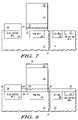
- FIGS. 1–16 of the drawingsillustrate a series of partial side views of a semiconductor device during various stages of manufacture of an integrated circuit according to a first embodiment of the present invention.
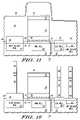
- FIGS. 1–10 and 16 – 23 of the drawingsillustrate a series of partial side views of a semiconductor device during various stages of manufacture of an integrated circuit according to a second embodiment of the present invention.
- FIGS. 1–16show partial side views of a semiconductor wafer during stages in the manufacture of a memory including nanoclusters according to a first embodiment of the present invention.
- the presently disclosed embodimentutilizes an intermediate dual polysilicon-nitride control electrode stack including a first formed polysilicon-nitride structure and a second formed polysilicon-nitride structure.
- the second formed polysilicon-nitride structureis removed while periphery device control electrodes are patterned, leaving first formed polysilicon-nitride control electrode structure for the memory cell devices.
- Such a techniqueallows protection of a top portion of a nanocluster oxide layer, thereby preserving thickness and quality of such oxide layer.
- FIG. 1shows a semiconductor device 10 .
- Semiconductor device 10is an integrated circuit die.
- Semiconductor device 10includes substrate 12 which is part of an overall wafer at the presently illustrated stage of manufacture.
- Semiconductor device 10also includes various dopant wells 14 , 18 and 20 which form part of the functional circuitry of semiconductor device 10 .
- Substratealso includes various pre-formed shallow trench isolation structures (not shown) to separate different devices and to laterally separate the wells discussed herein.
- Semiconductor device 10also includes a bottom oxide layer 22 .
- NVM well 18forms part of storage cell circuitry of a non-volatile memory array.
- NVM well 18is a p-well in which an array of storage cells will reside.
- periphery devicesinclude only high voltage (HV) devices (e.g., cell charge/discharge devices), in the embodiments discussed herein, periphery devices include various devices outside the NVM storage cell array and may include HV devices, integrated circuit die input/output (I/O) devices, and low (LV) voltage devices (e.g., logic devices).
- HVhigh voltage
- I/Ointegrated circuit die input/output
- LVlow
- High voltage (HV) well 14forms part of circuitry (e.g., high voltage transistors) for programming and erasing cells of the NVM array.
- the illustrated HV well 14is an n-well.
- Semiconductor devicemay alternatively or additionally include an HV p-well within a deep n-type isolation well.
- I/O well 20forms part of the I/O circuitry of semiconductor device 10 .
- the illustrated I/O well 20is an n-well.
- Semiconductor devicemay alternatively or additionally include an I/O p-well within a deep n-type isolation well.
- I/O well 20is a dual gate oxide (DGO) well.
- DGOdual gate oxide
- Silicon dioxide layer 22provides a tunnel dielectric layer.
- Other dielectricsmay be used for oxide layer 22 such as silicon oxynitride, hafnium oxide, aluminum oxide, lanthanum oxide, or lanthanum silicate.
- Dielectric layer 22has been formed over substrate 12 , for example, by oxidation or chemical vapor deposition. In one embodiment, bottom dielectric has thickness of 5 nanometers, but may be of other thicknesses in other embodiments.
- a layer of nanoclusters 24(e.g. of silicon, aluminum, gold, germanium, or a silicon and germanium alloy or other types of conductive material or doped or undoped semiconductive material) is formed over oxide layer 22 by, e.g., chemical vapor deposition techniques, aerosol deposition techniques, spin on coating techniques, or self assembly techniques such as annealing a thin film to form nanoclusters.
- the nanoclusters 24are silicon nanocrystals.
- the nanoclustershave a planar density of 1 ⁇ 10 ⁇ 12 cm ⁇ 2 with a size of 5 to 7 nanometers.
- nanoclustersare from 10–100 Angstroms in size. However the nanoclusters in other embodiments may be of other sizes and/or other densities.
- nanoclusters 24are separated by average distance generally equal to an average size of clusters. The average distance in one such embodiment is greater than 4 nanometers. Although nanoclusters 24 are shown as having a uniform size and distribution, nanoclusters 24 will have nonuniform sizes and a nonuniform distribution in actual practice. Nanoclusters 24 will be utilized for implementing charge storage locations in transistors (see FIG. 16 ) of a non-volatile memory of semiconductor device 10 .
- a layer of dielectric materiale.g. silicon dioxide, silicon oxynitride, hafnium oxide, aluminum oxide, lanthanum oxide, and lanthanum silicate
- a silicon dioxide layeris deposited over the nanoclusters.
- other dielectricssuch as silicon oxynitride, hafnium oxide, aluminum oxide, lanthanum oxide, or lanthanum silicate may be used for layer 26 .
- dielectric layer 26has a thickness of approximately 5–15 nanometers, but may be of other thicknesses in other embodiments.
- the bottom dielectric 22 , nanoclusters 24 , and control dielectric 26may be formed by ion implantation (e.g. silicon or germanium) into a layer of dielectric material (not shown) followed by the annealing of the ions to form nanocrystals in the layer of dielectric material.
- bottom dielectric 22 , nanoclusters 24 and control dielectric 26may be formed by recrystallization of a silicon rich oxide layer between two layers of dielectric material to form the nanoclusters.
- the nanoclustersmay be implemented in multiple layers located above the bottom dielectric.
- the nanoclustersare formed by depositing a thin amorphous layer of nanocluster material (e.g. 1–5 nanometers) wherein the resultant structure is annealed in a subsequent annealing process.
- a doped polysilicon layer 28is formed over dielectric layer 26 .
- a portion of polysilicon layer 28will serve as a gate electrode of an NVM bit cell.
- the polysilicon layermay be in situ doped (during deposition) or by implantation (after deposition). Other gate electrode materials may be used such as metals.
- an anti-reflective coatingARC
- silicon nitride layer 30provides the anti-reflective coating.
- a masking layer 32(e.g., a photoresist) is formed over nitride layer 30 .
- Masking layer 32protects the gate stack over NVM well 18 and exposes portions of layers 30 , 28 , 26 , 24 and 22 from other areas of semiconductor device 10 .
- Nitride layer 30 , polysilicon layer 28 , dielectric layer 26 and nanocluster layer 24are subsequently removed. Part of layer 22 is also subsequently removed.
- reactive ion etchingis used to remove layers 30 , 28 , 26 , 24 and 22 .
- tunnel dielectric layer 22is silicon dioxide
- the removalmay be performed via a wet etch using dilute hydrofluoric acid.
- the high voltage device oxide layer 34is formed.
- HV oxide layer 34may be grown by oxidation in oxygen or steam.
- One exemplary oxide layer 34is silicon dioxide having a thickness between 5 and 15 nanometers.
- Oxide layer 35is concomitantly grown over nitride layer 30 , typically having a smaller thickness.
- the nitride layer 30serves as a diffusion barrier and protects the underlying nanoclusters 24 , the polysilicon layer 26 , and tunnel dielectric 22 from deleterious oxidation.
- Such oxidationif allowed to occur, can adversely influence the NVM device performance since programming and erasing of the nanoclusters is very sensitive to the dielectric layer 22 thickness and the nanocluster size.
- the low voltage device wells 37 for general logic circuitryare formed by implantation into substrate 12 .
- a conventional implantation processfollows the opening of the low voltage areas by a masking step.
- the HV oxide layer 34serves as a sacrificial oxide for the low voltage well implants.
- the logic wellis activated typically by a rapid thermal annealing process.
- masking layer 36(e.g., a photoresist) is formed over HV oxide layer 34 to protect portions of the HV oxide layer over the HV device well 14 and to expose other portions of the HV oxide layer.
- exposed portions of the HV oxide layer 34are removed via a wet etch using dilute hydrofluoric acid.
- Oxide layer 35is removed concomitantly with exposed portions of layer 34 .
- the masking layer 36is also removed.
- I/O device oxide layer 38is formed. Although other methods may be used, oxide layer 38 is typically grown by oxidation in oxygen. Other oxygen compounds such as N 2 O may be used.
- One exemplary oxide layer 38is silicon dioxide.
- I/O oxide layer 38is generally slightly thinner than HV oxide layer 34 , having a thickness between 4 and 8 nanometers.
- Thin oxide layer 39is concomitantly grown over nitride layer 30 .
- HV oxide layer 34is naturally thickened during the growth of I/O oxide layer 38 .
- the nitride layer 30again serves as a diffusion barrier and protects the underlying nanoclusters 24 and tunnel dielectric 22 from deleterious oxidation. Such oxidation, if allowed to occur, can adversely influence the NVM device performance since programming and erasing of the nanoclusters is very sensitive to the dielectric layer 22 thickness and the nanocluster size.
- masking layer 40(e.g., a photoresist) is formed over I/O oxide layer 38 to protect portions of the HV and I/O oxide layers 34 and 38 over respective HV and I/O device wells 14 and 20 , and to expose other portions of the I/O oxide layer.
- the exposed portions of I/O oxide layer 38are removed using, for example, a wet etch of dilute hydrofluoric acid. Concomitantly, thin oxide layer 39 over nitride layer 30 is also removed.
- LV oxide 42is formed. Although other methods may be used, oxide layer 42 is typically grown by oxidation in oxygen, N 2 O or NO. One exemplary oxide layer 42 is silicon dioxide. LV oxide layer 42 is generally slightly thinner than HV oxide layer 34 and I/O oxide layer 38 , having a thickness between 1.5 and 3 nanometers. A very thin oxide layer 43 may be concomitantly grown over nitride layer 30 . HV oxide layer 34 and I/O oxide layer 38 may be naturally thickened during the growth of LV oxide layer 42 . During this oxidation step, the nitride layer 30 again serves as a diffusion barrier and protects the underlying nanoclusters 24 and tunnel dielectric 22 from any further oxidation.
- nitride layer 30again serves as a diffusion barrier and protects the underlying nanoclusters 24 and tunnel dielectric 22 from any further oxidation.
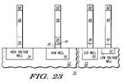
- a doped polysilicon layer 44is formed over substrate 12 .
- polysilicon layer 44is deposited over LV oxide layer 42 , HV oxide layer 34 , I/O oxide layer 38 and incidental oxide layer 43 .
- Portions of polysilicon layer 44will serve as gate electrodes of HV, LV and I/O devices.
- the two layersare approximately the same thickness. In other embodiments, different materials with appropriate thicknesses may be used for periphery and NVM array gate electrodes.
- Polysilicon layer 44may be in situ doped (during deposition) or by implantation (after deposition). Other gate electrode materials may be used such as metals.
- an anti-reflective coatingARC
- silicon nitride layer 46provides the anti-reflective coating.
- masking layer 48(e.g., a photoresist) is formed on nitride layer 46 over periphery devices and serves to pattern the gates for such devices, after which the exposed portions of layers 44 and 46 are removed using, for example, an anisotropic plasma etch.
- this gate patterning stepportions of polysilicon layer 44 and nitride layer 46 overlying the NVM areas are removed while the gate electrodes (e.g., portions of layer 44 ) of the LV, HV and I/O devices are allowed to remain.
- Using a reactive ion etch selective to the layers 43 and 30results in a substantially complete removal of the gate electrode material layer 44 and ARC layer 46 from over the NVM array area while simultaneously patterning the gate electrodes for the I/O, HV and LV devices.
- masking layer 48is removed.
- a masking layer 50(e.g., a photoresist) is formed over periphery device areas corresponding to HV well 14 , I/O well 20 and LV well 37 and other areas.
- the masking layerserves to pattern the gate electrodes for NVM array devices and to protect the periphery portions of semiconductor device 10 .
- various portions of layers exposed by masking layer 50are removed (e.g., via a nonselective, anisotropic, timed, plasma etch). For example, exposed portions thin oxide layer 43 , nitride ARC layer 30 , gate electrode layer 28 , control dielectric 26 and nanocluster layer 24 are removed. Part of tunnel dielectric layer 22 is also removed.
- masking layer 50is removed. Any remaining exposed portions of low voltage oxide layer 42 , high voltage oxide layer 34 , NVM tunnel dielectric 22 and I/O oxide layer 38 are removed by using wet etch processes. Very thin oxide 43 over the NVM ARC layer 30 is also removed. In an embodiment where all the oxide layers 34 , 38 and 42 are silicon dioxide, a dilute hydrofluoric acid wet clean can be employed for this purpose.
- the NVM cell and periphery devicesare completed.
- standard CMOS processing techniquesare used to form source/drain extensions, side-wall spacers and source/drain regions.
- 60 and 62represent source/drain regions and extension of an HV device
- 64 and 66represent source/drain regions and extension of an NVM cell
- 68 and 70represent source/drain regions and extension of an I/O device
- 72 and 74represent source/drain regions and extension of an LV device.
- Side-wall spacers 52correspond to an HV device
- side-wall spacers 54correspond to an NVM cell device
- side-wall spacers 56correspond to an I/O device
- side-wall spacers 58correspond to an LV device.
- a doped polysilicon layer 44may be formed over substrate 12 as illustrated in FIG. 17 .
- polysilicon layer 44is deposited over LV oxide layer 42 , HV oxide layer 34 , I/O oxide layer 38 and incidental oxide layer 43 . Portions of polysilicon layer 44 will serve as gate electrodes of HV, LV and I/O devices.
- an anti-reflective coating (ARC)is not required at this stage because subsequent etching is for large area and not for a critical dimension.
- a masking layer 80(e.g., a photoresist) is formed and patterned over the HV, I/O and LV areas and exposing the NVM well area.
- the polysilicon layer 44 , thin oxide layer 43 and nitride layer 30are etched over the NVM area using, for example, a dry etch, a wet etch or combination thereof. In one embodiment, the etch is stopped as a change in chemistry of the materials being etched is detected.
- masking layer 80is removed (e.g., via a plasma ash process or a piranha resist strip), and an ARC layer 82 is conformally deposited over polysilicon layers 44 and 28 .
- silicon nitrideis used to provide the anti-reflective coating.
- masking layer 84is formed over the HV, I/O, LV and NVM areas.
- a dry etchis performed to remove ARC layer 82 and the underlying polysilicon layers 44 and 28 , thereby exposing dielectric layers 26 , 34 , 38 and 42 .
- masking layer 84is removed (e.g., as discussed above with regard to masking layer 80 ), and the formation of the gate electrodes is continued by removing (e.g., etching) the exposed portions of dielectric layers 26 , 34 , 38 and 42 and layer 24 .
- processingcontinues in a similar fashion as described above with regard to FIG. 16 .
- This alternative embodimentprovides the advantage that only one of two masks has critical dimensions which provides cost and manufacturing advantages.
- a method of forming a nanocluster charge storage deviceis provided.
- a substrateis provided.
- the substratehas a first dopant well associated with the nanocluster charge storage device and a second dopant well associated with a semiconductor device not having nanoclusters.
- a first gate stackis formed overlying the first dopant well and having a first conductive gate material layer that forms a gate electrode in the first gate stack.
- the first conductive gate material layeroverlies a plurality of nanoclusters embedded in a first gate dielectric layer.
- the first conductive gate material layerunderlies a portion of a second conductive gate material layer.
- a second gate stackis formed overlying the second dopant well using a portion of the second conductive gate material layer overlying the second dopant well as a gate electrode in the second gate stack. A portion of the second conductive gate material layer that overlies the first conductive gate material layer is removed.
- the portion of the second conductive gate material layer that overlies the first conductive gate material layeris removed by masking all areas away from the first dopant well and selectively etching the second conductive gate material layer.
- the first conductive gate material layer and the second conductive gate material layerare formed using doped polysilicon, a metal or a metal alloy.
- the first conductive gate material layeris implemented with a material that is different from the second conductive gate material layer.
- the forming of the first gate dielectric layeris by forming a gate oxide layer and a second gate oxide layer overlying and surrounding the nanocluster layer.
- the first gate dielectric and the first conductive gate material layerare formed overlying both the first dopant well and the second dopant well. Selectively etching from areas overlying the second dopant well of the first conductive gate material layer occurs, the first gate dielectric layer and the nanocluster layer using a combination of a wet etch and a dry etch.
- the second gate stackis formed by forming a second gate dielectric layer and the second conductive gate material layer overlying a portion of the second dopant well.
- the second conductive gate material layeroverlies the second gate dielectric layer.
- the second gate dielectric layeris formed of silicon dioxide or silicon oxynitride.
- a nitride layeris formed in the first gate stack and overlies the first conductive gate material and is between a portion of the first conductive gate material and the second conductive gate material.
- An oxide layeris formed overlying and in physical contact with the nitride layer. The nitride layer and oxide layer function as an etch stop layer when removing the second conductive gate material. The nitride layer also functions as an antireflective coating when forming the gate electrode in the first gate stack.
- the first gate dielectric layeris formed of an oxide or an oxynitride of a compound containing at least one of hafnium, lanthanum, aluminum and silicon.
- the plurality of nanoclusters embedded in the first gate dielectric layer overlying the first dopant well and the second dopant wellare formed by forming a layer of doped or undoped semiconductor nanocrystals, metal nanocrystals, nanocrystals of two or more doped or undoped semiconductors, or metal alloy nanocrystals.
- a first source and a first drainare formed around the first gate stack and within the first dopant well to form the charge storage device as a nonvolatile memory (NVM) transistor.
- a second source and a second drainare formed around the second gate stack and within the second dopant well to form a periphery transistor.
- a semiconductor deviceis formed from the second gate stack.
- the semiconductor deviceenables charging and discharging of the nanocluster charge storage device.
- a methodincludes the following steps: providing a substrate; forming a first dopant well and a second dopant well in the substrate; forming a layer of nanoclusters embedded in a first gate dielectric overlying the first dopant well and the second dopant well; forming a first conductive gate material layer overlying the layer of nanoclusters; forming a nitride layer overlying the first conductive gate material layer; forming a storage stack overlying the first dopant well by patterning and removing the nitride layer, the first conductive gate material layer, and the layer of nanoclusters from areas other than overlying the first dopant well; forming a second gate dielectric overlying the second dopant well, the second gate dielectric having no nanoclusters; forming a second conductive gate material layer overlying the second gate dielectric and the storage stack; forming an anti-reflective coating layer overlying the second conductive gate material layer; patterning the second conductive gate
- the methodfurther includes the following steps: forming a first source and a first drain around the first gate stack and within the second dopant well to form a transistor; and forming a second source and a second drain around the second gate stack and within the first dopant well to complete formation of the charge storage device.
- the methodfurther includes the step of forming the first conductive gate material layer of doped polysilicon, metal or a metal alloy.
- the methodfurther includes the step of forming the second conductive gate material layer ( 44 ) of doped polysilicon, metal or a metal alloy
- the methodfurther includes the step of forming the layer of nanoclusters embedded in the first gate dielectric overlying the first dopant well and the second dopant well by forming a layer of doped or undoped semiconductor nanocrystals, metal nanocrystals, nanocrystals of two or more doped or undoped semiconductors, or metal alloy nanocrystals.
- the methodfurther includes the step of forming the first gate dielectric of an oxide or an oxynitride of a compound containing at least one of hafnium, lanthanum, aluminum and silicon.
- the methodfurther includes the step of forming the second gate dielectric of silicon dioxide or silicon oxynitride.
- a method of forming a nanocluster charge storage deviceincludes the following steps: providing a substrate having a memory dopant well associated with the nanocluster charge storage device and a periphery dopant well associated with a semiconductor device not having nanoclusters; forming a layer of nanoclusters embedded in a first gate dielectric overlying the memory dopant well; forming a first gate material layer overlying the layer of nanoclusters; patterning the layer of nanoclusters and the first gate material layer to exist only overlying the memory dopant well; forming a second gate material layer overlying the periphery dopant well and also overlying the layer of nanoclusters and the first gate material layer after formation of the first gate material layer; forming a periphery device gate stack by removing the second gate material layer from areas other than a predetermined periphery area overlying the periphery dopant well; and subsequently forming a nanocluster charge storage device gate stack by patterning the layer
- the methodfurther includes forming an etch stop layer directly overlying the first gate material layer for endpoint detection during removal of the second gate material layer overlying the first gate material layer.
- a method of forming a nanocluster charge storage deviceincludes: providing a substrate having a memory dopant well associated with the nanocluster charge storage device and a periphery dopant well associated with a semiconductor device not having nanoclusters; forming a layer of nanoclusters embedded in a first gate dielectric overlying the memory dopant well; forming a first gate material layer overlying the layer of nanoclusters; patterning the layer of nanoclusters and the first gate material layer to exist only overlying the memory dopant well; forming a second gate material layer overlying the periphery dopant well and also overlying the layer of nanoclusters and the first gate material layer after formation of the first gate material layer; removing the second gate material layer from areas other than a predetermined periphery area overlying the periphery dopant well; and using a mask to selectively form at a substantially same time a periphery device gate stack and a nanocluster charge storage gate.
- Many of the devices described hereinmay be conceptualized as having a control terminal which controls the flow of current between a first current handling terminal and a second current handling terminal.
- a control terminalwhich controls the flow of current between a first current handling terminal and a second current handling terminal.
- One example of such a deviceis a transistor.
- An appropriate condition on the control terminal of a transistorcauses a current to flow from/to the first current handling terminal and to/from the second current handling terminal.
- FETsfield effect transistors
- FETsfield effect transistors
- the drainis interchangeable with the source. This is because the layout and semiconductor processing of the transistor is frequently symmetrical.
- the claimreads on the apparatus or method regardless of whether the apparatus or method includes another such similar feature.
- This use of the word “a” as a nonlimiting, introductory article to a feature of a claimis adopted herein by Applicants as being identical to the interpretation adopted by many courts in the past, notwithstanding any anomalous or precedential case law to the contrary that may be found.
- a claim elementis described in the claims below as including or comprising an aforementioned feature (e.g., “the” feature), it is intended that the element not be limited to one and only one of the feature described merely by the incidental use of the definite article.
Landscapes
- Engineering & Computer Science (AREA)
- Chemical & Material Sciences (AREA)
- Nanotechnology (AREA)
- Physics & Mathematics (AREA)
- Mathematical Physics (AREA)
- Theoretical Computer Science (AREA)
- Crystallography & Structural Chemistry (AREA)
- Manufacturing & Machinery (AREA)
- Non-Volatile Memory (AREA)
- Semiconductor Memories (AREA)
- Formation Of Insulating Films (AREA)
Abstract
Description
Claims (22)
Priority Applications (6)
| Application Number | Priority Date | Filing Date | Title |
|---|---|---|---|
| US10/876,820US7091130B1 (en) | 2004-06-25 | 2004-06-25 | Method of forming a nanocluster charge storage device |
| CNB2005800210850ACN100435286C (en) | 2004-06-25 | 2005-05-11 | Method for forming nanocluster charge storage devices |
| PCT/US2005/016252WO2006007069A2 (en) | 2004-06-25 | 2005-05-11 | Method of forming a nanocluster charge storage device |
| EP05782558AEP1759405A4 (en) | 2004-06-25 | 2005-05-11 | METHOD FOR FORMING A NANOAGREGATE LOAD STORAGE DEVICE |
| JP2007518062AJP2008504679A (en) | 2004-06-25 | 2005-05-11 | Method of forming a nanocluster charge storage device |
| TW094119327ATWI375318B (en) | 2004-06-25 | 2005-06-10 | Method of forming a nanocluster charge storage device |
Applications Claiming Priority (1)
| Application Number | Priority Date | Filing Date | Title |
|---|---|---|---|
| US10/876,820US7091130B1 (en) | 2004-06-25 | 2004-06-25 | Method of forming a nanocluster charge storage device |
Publications (2)
| Publication Number | Publication Date |
|---|---|
| US7091130B1true US7091130B1 (en) | 2006-08-15 |
| US20060194438A1 US20060194438A1 (en) | 2006-08-31 |
Family
ID=35784282
Family Applications (1)
| Application Number | Title | Priority Date | Filing Date |
|---|---|---|---|
| US10/876,820Expired - LifetimeUS7091130B1 (en) | 2004-06-25 | 2004-06-25 | Method of forming a nanocluster charge storage device |
Country Status (6)
| Country | Link |
|---|---|
| US (1) | US7091130B1 (en) |
| EP (1) | EP1759405A4 (en) |
| JP (1) | JP2008504679A (en) |
| CN (1) | CN100435286C (en) |
| TW (1) | TWI375318B (en) |
| WO (1) | WO2006007069A2 (en) |
Cited By (13)
| Publication number | Priority date | Publication date | Assignee | Title |
|---|---|---|---|---|
| US20060105522A1 (en)* | 2004-11-12 | 2006-05-18 | Steimle Robert F | Method of forming a nanocluster charge storage device |
| US20060105524A1 (en)* | 2004-11-15 | 2006-05-18 | Samsung Electronics Co., Ltd. | Non-volatile device manufactured using ion-implantation and method of manufacture the same |
| US20060160311A1 (en)* | 2005-01-14 | 2006-07-20 | Rao Rajesh A | Method of forming an integrated circuit having nanocluster devices and non-nanocluster devices |
| US20080269748A1 (en)* | 2007-04-24 | 2008-10-30 | Osteolign | Deformable Implant Systems and Methods |
| US20100159651A1 (en)* | 2008-12-19 | 2010-06-24 | Shen Jinmiao J | Method of forming nanocrystals |
| US7871886B2 (en) | 2008-12-19 | 2011-01-18 | Freescale Semiconductor, Inc. | Nanocrystal memory with differential energy bands and method of formation |
| US8883624B1 (en)* | 2013-09-27 | 2014-11-11 | Cypress Semiconductor Corporation | Integration of a memory transistor into high-K, metal gate CMOS process flow |
| US9023707B1 (en) | 2009-04-24 | 2015-05-05 | Cypress Semiconductor Corporation | Simultaneously forming a dielectric layer in MOS and ONO device regions |
| US9299568B2 (en) | 2007-05-25 | 2016-03-29 | Cypress Semiconductor Corporation | SONOS ONO stack scaling |
| US20160133636A1 (en)* | 2013-06-21 | 2016-05-12 | Taiwan Semiconductor Manufacturing Co., Ltd. | Embedded Flash Memory Device with Floating Gate Embedded in a Substrate |
| US9349877B1 (en) | 2007-05-25 | 2016-05-24 | Cypress Semiconductor Corporation | Nitridation oxidation of tunneling layer for improved SONOS speed and retention |
| US10615289B2 (en) | 2007-12-12 | 2020-04-07 | Longitude Flash Memory Solutions Ltd. | Nonvolatile charge trap memory device having a high dielectric constant blocking region |
| US10700083B1 (en) | 2009-04-24 | 2020-06-30 | Longitude Flash Memory Solutions Ltd. | Method of ONO integration into logic CMOS flow |
Families Citing this family (24)
| Publication number | Priority date | Publication date | Assignee | Title |
|---|---|---|---|---|
| US7589029B2 (en) | 2002-05-02 | 2009-09-15 | Micron Technology, Inc. | Atomic layer deposition and conversion |
| US7588988B2 (en) | 2004-08-31 | 2009-09-15 | Micron Technology, Inc. | Method of forming apparatus having oxide films formed using atomic layer deposition |
| US20060131633A1 (en)* | 2004-12-21 | 2006-06-22 | Micron Technology, Inc. | Integrated two device non-volatile memory |
| US7662729B2 (en) | 2005-04-28 | 2010-02-16 | Micron Technology, Inc. | Atomic layer deposition of a ruthenium layer to a lanthanide oxide dielectric layer |
| US7572695B2 (en) | 2005-05-27 | 2009-08-11 | Micron Technology, Inc. | Hafnium titanium oxide films |
| US7927948B2 (en) | 2005-07-20 | 2011-04-19 | Micron Technology, Inc. | Devices with nanocrystals and methods of formation |
| US7575978B2 (en)* | 2005-08-04 | 2009-08-18 | Micron Technology, Inc. | Method for making conductive nanoparticle charge storage element |
| US7410910B2 (en) | 2005-08-31 | 2008-08-12 | Micron Technology, Inc. | Lanthanum aluminum oxynitride dielectric films |
| KR100698086B1 (en)* | 2005-12-29 | 2007-03-23 | 동부일렉트로닉스 주식회사 | Manufacturing method of semiconductor device |
| US7955935B2 (en)* | 2006-08-03 | 2011-06-07 | Micron Technology, Inc. | Non-volatile memory cell devices and methods |
| US7560769B2 (en) | 2006-08-03 | 2009-07-14 | Micron Technology, Inc. | Non-volatile memory cell device and methods |
| US8093680B1 (en)* | 2006-09-14 | 2012-01-10 | Spansion Llc | Metal-insulator-metal-insulator-metal (MIMIM) memory device |
| US7687349B2 (en) | 2006-10-30 | 2010-03-30 | Atmel Corporation | Growth of silicon nanodots having a metallic coating using gaseous precursors |
| FR2910176B1 (en)* | 2006-12-15 | 2009-10-23 | Commissariat Energie Atomique | METHOD FOR PRODUCING A DEVICE BASED ON NANOCRYSTALS COATED WITH A CVD-BASED NITRIDE LAYER |
| US7763511B2 (en)* | 2006-12-29 | 2010-07-27 | Intel Corporation | Dielectric barrier for nanocrystals |
| US7816211B2 (en) | 2007-01-26 | 2010-10-19 | Freescale Semiconductor, Inc. | Method of making a semiconductor device having high voltage transistors, non-volatile memory transistors, and logic transistors |
| US8367506B2 (en) | 2007-06-04 | 2013-02-05 | Micron Technology, Inc. | High-k dielectrics with gold nano-particles |
| US7846793B2 (en)* | 2007-10-03 | 2010-12-07 | Applied Materials, Inc. | Plasma surface treatment for SI and metal nanocrystal nucleation |
| US8202778B2 (en)* | 2010-08-31 | 2012-06-19 | Freescale Semiconductor, Inc. | Patterning a gate stack of a non-volatile memory (NVM) with simultaneous etch in non-NVM area |
| US8679912B2 (en)* | 2012-01-31 | 2014-03-25 | Freescale Semiconductor, Inc. | Semiconductor device having different non-volatile memories having nanocrystals of differing densities and method therefor |
| JP5732574B2 (en)* | 2014-04-14 | 2015-06-10 | ルネサスエレクトロニクス株式会社 | Manufacturing method of semiconductor device |
| US9218978B1 (en)* | 2015-03-09 | 2015-12-22 | Cypress Semiconductor Corporation | Method of ONO stack formation |
| CN107978606B (en)* | 2017-11-20 | 2020-08-25 | 上海华力微电子有限公司 | Embedded flash memory process integration method |
| TWI704648B (en)* | 2019-11-20 | 2020-09-11 | 華邦電子股份有限公司 | Method for manufacturing memory device |
Citations (8)
| Publication number | Priority date | Publication date | Assignee | Title |
|---|---|---|---|---|
| US6297095B1 (en) | 2000-06-16 | 2001-10-02 | Motorola, Inc. | Memory device that includes passivated nanoclusters and method for manufacture |
| US6320784B1 (en) | 2000-03-14 | 2001-11-20 | Motorola, Inc. | Memory cell and method for programming thereof |
| US6444545B1 (en) | 2000-12-19 | 2002-09-03 | Motorola, Inc. | Device structure for storing charge and method therefore |
| US20040135204A1 (en)* | 2002-06-05 | 2004-07-15 | Hongmei Wang | Fully-depleted (FD) (SOI) MOSFET access transistor and method of fabrication |
| US20040212019A1 (en) | 2003-04-28 | 2004-10-28 | Masaaki Shinohara | Semiconductor device and a method of manufacturing the same |
| US20050098822A1 (en) | 2003-11-10 | 2005-05-12 | Leo Mathew | Transistor having three electrically isolated electrodes and method of formation |
| US6958265B2 (en)* | 2003-09-16 | 2005-10-25 | Freescale Semiconductor, Inc. | Semiconductor device with nanoclusters |
| US7015090B2 (en) | 2002-04-17 | 2006-03-21 | Renesas Technology Corp. | Method of manufacturing a semiconductor device having trenches for isolation and capacitor formation trenches |
Family Cites Families (10)
| Publication number | Priority date | Publication date | Assignee | Title |
|---|---|---|---|---|
| TW420874B (en)* | 1998-05-04 | 2001-02-01 | Koninkl Philips Electronics Nv | Method of manufacturing a semiconductor device |
| JP2000077618A (en)* | 1998-06-15 | 2000-03-14 | Mitsubishi Electric Corp | Semiconductor device and method of manufacturing the same |
| EP1107309B1 (en)* | 1999-12-06 | 2010-10-13 | STMicroelectronics Srl | Manufacturing process for non-volatile floating gate memory cells and control circuitry |
| JP2002009168A (en)* | 2000-06-19 | 2002-01-11 | Nec Corp | Semiconductor device and manufacturing method thereof |
| JP4096507B2 (en)* | 2000-09-29 | 2008-06-04 | 富士通株式会社 | Manufacturing method of semiconductor device |
| JP4322477B2 (en)* | 2001-06-28 | 2009-09-02 | 株式会社東芝 | Manufacturing method of semiconductor device |
| JP2003218245A (en)* | 2002-01-25 | 2003-07-31 | Sony Corp | Method of manufacturing non-volatile semiconductor memory device |
| JP3993438B2 (en)* | 2002-01-25 | 2007-10-17 | 株式会社ルネサステクノロジ | Semiconductor device |
| US7115949B2 (en)* | 2002-05-30 | 2006-10-03 | Freescale Semiconductor, Inc. | Method of forming a semiconductor device in a semiconductor layer and structure thereof |
| JP2004104009A (en)* | 2002-09-12 | 2004-04-02 | Fujitsu Ltd | Semiconductor device and manufacturing method thereof |
- 2004
- 2004-06-25USUS10/876,820patent/US7091130B1/ennot_activeExpired - Lifetime
- 2005
- 2005-05-11JPJP2007518062Apatent/JP2008504679A/enactivePending
- 2005-05-11CNCNB2005800210850Apatent/CN100435286C/ennot_activeExpired - Fee Related
- 2005-05-11EPEP05782558Apatent/EP1759405A4/ennot_activeWithdrawn
- 2005-05-11WOPCT/US2005/016252patent/WO2006007069A2/ennot_activeApplication Discontinuation
- 2005-06-10TWTW094119327Apatent/TWI375318B/ennot_activeIP Right Cessation
Patent Citations (8)
| Publication number | Priority date | Publication date | Assignee | Title |
|---|---|---|---|---|
| US6320784B1 (en) | 2000-03-14 | 2001-11-20 | Motorola, Inc. | Memory cell and method for programming thereof |
| US6297095B1 (en) | 2000-06-16 | 2001-10-02 | Motorola, Inc. | Memory device that includes passivated nanoclusters and method for manufacture |
| US6444545B1 (en) | 2000-12-19 | 2002-09-03 | Motorola, Inc. | Device structure for storing charge and method therefore |
| US7015090B2 (en) | 2002-04-17 | 2006-03-21 | Renesas Technology Corp. | Method of manufacturing a semiconductor device having trenches for isolation and capacitor formation trenches |
| US20040135204A1 (en)* | 2002-06-05 | 2004-07-15 | Hongmei Wang | Fully-depleted (FD) (SOI) MOSFET access transistor and method of fabrication |
| US20040212019A1 (en) | 2003-04-28 | 2004-10-28 | Masaaki Shinohara | Semiconductor device and a method of manufacturing the same |
| US6958265B2 (en)* | 2003-09-16 | 2005-10-25 | Freescale Semiconductor, Inc. | Semiconductor device with nanoclusters |
| US20050098822A1 (en) | 2003-11-10 | 2005-05-12 | Leo Mathew | Transistor having three electrically isolated electrodes and method of formation |
Non-Patent Citations (5)
| Title |
|---|
| Attorney Docket No. SC13087TP filed concurrently. |
| Cavins et al., "A Nitride-Oxide Blocking Layer for Scaled SONOS Non-Volatile Memory," Motorola, Inc., Jan. 10, 2002, 5 pages. |
| Cavins et al., "Integrated Stacked Gate Oxide and Interpoly Oxide," Motorola, Inc.,, Nov. 1996, pp. 93-94. |
| S., Wolf, Silicon Processing for the VLSI Era, vol. 4, Lattice Press Press (2002) pp. 385-386.* |
| U.S. Appl. No. 10/987,047, filed Nov. 12, 2004. |
Cited By (30)
| Publication number | Priority date | Publication date | Assignee | Title |
|---|---|---|---|---|
| US20060105522A1 (en)* | 2004-11-12 | 2006-05-18 | Steimle Robert F | Method of forming a nanocluster charge storage device |
| US7361543B2 (en)* | 2004-11-12 | 2008-04-22 | Freescale Semiconductor, Inc. | Method of forming a nanocluster charge storage device |
| US20080105945A1 (en)* | 2004-11-12 | 2008-05-08 | Freescale Semiconductor, Inc. | Method of forming a nanocluster charge storage device |
| US8373221B2 (en) | 2004-11-12 | 2013-02-12 | Freescale Semiconductor, Inc. | Nanocluster charge storage device |
| US20060105524A1 (en)* | 2004-11-15 | 2006-05-18 | Samsung Electronics Co., Ltd. | Non-volatile device manufactured using ion-implantation and method of manufacture the same |
| US20060160311A1 (en)* | 2005-01-14 | 2006-07-20 | Rao Rajesh A | Method of forming an integrated circuit having nanocluster devices and non-nanocluster devices |
| US7183159B2 (en)* | 2005-01-14 | 2007-02-27 | Freescale Semiconductor, Inc. | Method of forming an integrated circuit having nanocluster devices and non-nanocluster devices |
| US20080269748A1 (en)* | 2007-04-24 | 2008-10-30 | Osteolign | Deformable Implant Systems and Methods |
| US10699901B2 (en) | 2007-05-25 | 2020-06-30 | Longitude Flash Memory Solutions Ltd. | SONOS ONO stack scaling |
| US9997641B2 (en) | 2007-05-25 | 2018-06-12 | Cypress Semiconductor Corporation | SONOS ONO stack scaling |
| US9349877B1 (en) | 2007-05-25 | 2016-05-24 | Cypress Semiconductor Corporation | Nitridation oxidation of tunneling layer for improved SONOS speed and retention |
| US9299568B2 (en) | 2007-05-25 | 2016-03-29 | Cypress Semiconductor Corporation | SONOS ONO stack scaling |
| US10615289B2 (en) | 2007-12-12 | 2020-04-07 | Longitude Flash Memory Solutions Ltd. | Nonvolatile charge trap memory device having a high dielectric constant blocking region |
| US20100159651A1 (en)* | 2008-12-19 | 2010-06-24 | Shen Jinmiao J | Method of forming nanocrystals |
| US7799634B2 (en) | 2008-12-19 | 2010-09-21 | Freescale Semiconductor, Inc. | Method of forming nanocrystals |
| US8163609B2 (en) | 2008-12-19 | 2012-04-24 | Freescale Semiconductor, Inc. | Nanocrystal memory with differential energy bands and method of formation |
| US20110073936A1 (en)* | 2008-12-19 | 2011-03-31 | Freescale Semiconductor, Inc. | Nanocrystal memory with differential energy bands and method of formation |
| US7871886B2 (en) | 2008-12-19 | 2011-01-18 | Freescale Semiconductor, Inc. | Nanocrystal memory with differential energy bands and method of formation |
| US12048162B2 (en) | 2009-04-24 | 2024-07-23 | Longitude Flash Memory Solutions Ltd. | Method of ono integration into logic CMOS flow |
| US9023707B1 (en) | 2009-04-24 | 2015-05-05 | Cypress Semiconductor Corporation | Simultaneously forming a dielectric layer in MOS and ONO device regions |
| US11569254B2 (en) | 2009-04-24 | 2023-01-31 | Longitude Flash Memory Solutions Ltd. | Method of ono integration into logic CMOS flow |
| US10700083B1 (en) | 2009-04-24 | 2020-06-30 | Longitude Flash Memory Solutions Ltd. | Method of ONO integration into logic CMOS flow |
| US20160133636A1 (en)* | 2013-06-21 | 2016-05-12 | Taiwan Semiconductor Manufacturing Co., Ltd. | Embedded Flash Memory Device with Floating Gate Embedded in a Substrate |
| US11903191B2 (en) | 2013-06-21 | 2024-02-13 | Taiwan Semiconductor Manufacturing Company, Ltd. | Embedded flash memory device with floating gate embedded in a substrate |
| US10163919B2 (en)* | 2013-06-21 | 2018-12-25 | Taiwan Semiconductor Manufacturing Company, Ltd. | Embedded flash memory device with floating gate embedded in a substrate |
| US9721962B1 (en) | 2013-09-27 | 2017-08-01 | Cypress Semiconductor Corporation | Integration of a memory transistor into high-k, metal gate CMOS process flow |
| US10784277B2 (en) | 2013-09-27 | 2020-09-22 | Longitude Flash Memory Solutions Ltd. | Integration of a memory transistor into High-k, metal gate CMOS process flow |
| US9911746B1 (en) | 2013-09-27 | 2018-03-06 | Cypress Semiconductor Corporation | Integration of a memory transistor into high-k, metal gate CMOS process flow |
| US9911747B2 (en) | 2013-09-27 | 2018-03-06 | Cypress Semiconductor Corporation | Integration of a memory transistor into high-k, metal gate CMOS process flow |
| US8883624B1 (en)* | 2013-09-27 | 2014-11-11 | Cypress Semiconductor Corporation | Integration of a memory transistor into high-K, metal gate CMOS process flow |
Also Published As
| Publication number | Publication date |
|---|---|
| TW200612548A (en) | 2006-04-16 |
| JP2008504679A (en) | 2008-02-14 |
| US20060194438A1 (en) | 2006-08-31 |
| WO2006007069A2 (en) | 2006-01-19 |
| EP1759405A2 (en) | 2007-03-07 |
| CN100435286C (en) | 2008-11-19 |
| TWI375318B (en) | 2012-10-21 |
| EP1759405A4 (en) | 2008-11-12 |
| CN101010785A (en) | 2007-08-01 |
| WO2006007069A3 (en) | 2007-04-12 |
Similar Documents
| Publication | Publication Date | Title |
|---|---|---|
| US7091130B1 (en) | Method of forming a nanocluster charge storage device | |
| US7361543B2 (en) | Method of forming a nanocluster charge storage device | |
| US7663179B2 (en) | Semiconductor device with rewritable nonvolatile memory cell | |
| US7348245B2 (en) | Semiconductor device and a method of manufacturing the same | |
| US7091089B2 (en) | Method of forming a nanocluster charge storage device | |
| US20080246073A1 (en) | Nonvolatile Memory Devices Including a Resistor Region | |
| US6787419B2 (en) | Method of forming an embedded memory including forming three silicon or polysilicon layers | |
| US20030211692A1 (en) | Method of fabricating trap type nonvolatile memory device | |
| US7029976B1 (en) | Method for SONOS EFLASH integrated circuit | |
| TWI555066B (en) | Semiconductor component manufacturing method | |
| JP3745297B2 (en) | Method for manufacturing nonvolatile semiconductor memory device | |
| US8030165B2 (en) | Poly gate etch method and device for sonos-based flash memory | |
| US6242773B1 (en) | Self-aligning poly 1 ono dielectric for non-volatile memory | |
| US6696331B1 (en) | Method of protecting a stacked gate structure during fabrication | |
| US6605501B1 (en) | Method of fabricating CMOS device with dual gate electrode | |
| US7772639B2 (en) | Charge-trap nonvolatile memory devices | |
| JP2004103902A (en) | Nonvolatile semiconductor storage device and its manufacturing method | |
| US6943119B2 (en) | Flash process for stacking poly etching | |
| KR20070023770A (en) | Nanocluster charge storage device formation method | |
| KR20070021271A (en) | How to Form Nanocluster Charge Storage Devices | |
| TW569402B (en) | Method of forming an embedded memory | |
| KR20090044411A (en) | Manufacturing method of charge trap element |
Legal Events
| Date | Code | Title | Description |
|---|---|---|---|
| AS | Assignment | Owner name:PREESCALE SEMICONDUCTOR, INC., TEXAS Free format text:ASSIGNMENT OF ASSIGNORS INTEREST;ASSIGNORS:RAO, RAJESH A.;MURALIDHAR, RAMACHANDRAN;STEIMLE, ROBERT F.;AND OTHERS;REEL/FRAME:015525/0428;SIGNING DATES FROM 20040623 TO 20040625 | |
| STCF | Information on status: patent grant | Free format text:PATENTED CASE | |
| AS | Assignment | Owner name:CITIBANK, N.A. AS COLLATERAL AGENT, NEW YORK Free format text:SECURITY AGREEMENT;ASSIGNORS:FREESCALE SEMICONDUCTOR, INC.;FREESCALE ACQUISITION CORPORATION;FREESCALE ACQUISITION HOLDINGS CORP.;AND OTHERS;REEL/FRAME:018855/0129 Effective date:20061201 Owner name:CITIBANK, N.A. AS COLLATERAL AGENT,NEW YORK Free format text:SECURITY AGREEMENT;ASSIGNORS:FREESCALE SEMICONDUCTOR, INC.;FREESCALE ACQUISITION CORPORATION;FREESCALE ACQUISITION HOLDINGS CORP.;AND OTHERS;REEL/FRAME:018855/0129 Effective date:20061201 | |
| FPAY | Fee payment | Year of fee payment:4 | |
| AS | Assignment | Owner name:CITIBANK, N.A., AS COLLATERAL AGENT,NEW YORK Free format text:SECURITY AGREEMENT;ASSIGNOR:FREESCALE SEMICONDUCTOR, INC.;REEL/FRAME:024397/0001 Effective date:20100413 Owner name:CITIBANK, N.A., AS COLLATERAL AGENT, NEW YORK Free format text:SECURITY AGREEMENT;ASSIGNOR:FREESCALE SEMICONDUCTOR, INC.;REEL/FRAME:024397/0001 Effective date:20100413 | |
| AS | Assignment | Owner name:CITIBANK, N.A., AS NOTES COLLATERAL AGENT, NEW YORK Free format text:SECURITY AGREEMENT;ASSIGNOR:FREESCALE SEMICONDUCTOR, INC.;REEL/FRAME:030633/0424 Effective date:20130521 Owner name:CITIBANK, N.A., AS NOTES COLLATERAL AGENT, NEW YOR Free format text:SECURITY AGREEMENT;ASSIGNOR:FREESCALE SEMICONDUCTOR, INC.;REEL/FRAME:030633/0424 Effective date:20130521 | |
| AS | Assignment | Owner name:CITIBANK, N.A., AS NOTES COLLATERAL AGENT, NEW YORK Free format text:SECURITY AGREEMENT;ASSIGNOR:FREESCALE SEMICONDUCTOR, INC.;REEL/FRAME:031591/0266 Effective date:20131101 Owner name:CITIBANK, N.A., AS NOTES COLLATERAL AGENT, NEW YOR Free format text:SECURITY AGREEMENT;ASSIGNOR:FREESCALE SEMICONDUCTOR, INC.;REEL/FRAME:031591/0266 Effective date:20131101 | |
| FPAY | Fee payment | Year of fee payment:8 | |
| AS | Assignment | Owner name:FREESCALE SEMICONDUCTOR, INC., TEXAS Free format text:PATENT RELEASE;ASSIGNOR:CITIBANK, N.A., AS COLLATERAL AGENT;REEL/FRAME:037356/0143 Effective date:20151207 Owner name:FREESCALE SEMICONDUCTOR, INC., TEXAS Free format text:PATENT RELEASE;ASSIGNOR:CITIBANK, N.A., AS COLLATERAL AGENT;REEL/FRAME:037356/0553 Effective date:20151207 Owner name:FREESCALE SEMICONDUCTOR, INC., TEXAS Free format text:PATENT RELEASE;ASSIGNOR:CITIBANK, N.A., AS COLLATERAL AGENT;REEL/FRAME:037354/0225 Effective date:20151207 | |
| AS | Assignment | Owner name:MORGAN STANLEY SENIOR FUNDING, INC., MARYLAND Free format text:ASSIGNMENT AND ASSUMPTION OF SECURITY INTEREST IN PATENTS;ASSIGNOR:CITIBANK, N.A.;REEL/FRAME:037486/0517 Effective date:20151207 | |
| AS | Assignment | Owner name:MORGAN STANLEY SENIOR FUNDING, INC., MARYLAND Free format text:ASSIGNMENT AND ASSUMPTION OF SECURITY INTEREST IN PATENTS;ASSIGNOR:CITIBANK, N.A.;REEL/FRAME:037518/0292 Effective date:20151207 | |
| AS | Assignment | Owner name:NORTH STAR INNOVATIONS INC., CALIFORNIA Free format text:ASSIGNMENT OF ASSIGNORS INTEREST;ASSIGNOR:FREESCALE SEMICONDUCTOR, INC.;REEL/FRAME:037694/0264 Effective date:20151002 | |
| AS | Assignment | Owner name:NXP, B.V., F/K/A FREESCALE SEMICONDUCTOR, INC., NETHERLANDS Free format text:RELEASE BY SECURED PARTY;ASSIGNOR:MORGAN STANLEY SENIOR FUNDING, INC.;REEL/FRAME:040925/0001 Effective date:20160912 Owner name:NXP, B.V., F/K/A FREESCALE SEMICONDUCTOR, INC., NE Free format text:RELEASE BY SECURED PARTY;ASSIGNOR:MORGAN STANLEY SENIOR FUNDING, INC.;REEL/FRAME:040925/0001 Effective date:20160912 | |
| AS | Assignment | Owner name:NXP B.V., NETHERLANDS Free format text:RELEASE BY SECURED PARTY;ASSIGNOR:MORGAN STANLEY SENIOR FUNDING, INC.;REEL/FRAME:040928/0001 Effective date:20160622 | |
| AS | Assignment | Owner name:MORGAN STANLEY SENIOR FUNDING, INC., MARYLAND Free format text:CORRECTIVE ASSIGNMENT TO CORRECT THE REMOVE PATENTS 8108266 AND 8062324 AND REPLACE THEM WITH 6108266 AND 8060324 PREVIOUSLY RECORDED ON REEL 037518 FRAME 0292. ASSIGNOR(S) HEREBY CONFIRMS THE ASSIGNMENT AND ASSUMPTION OF SECURITY INTEREST IN PATENTS;ASSIGNOR:CITIBANK, N.A.;REEL/FRAME:041703/0536 Effective date:20151207 | |
| AS | Assignment | Owner name:TAIWAN SEMICONDUCTOR MANUFACTURING CO., LTD., TAIW Free format text:ASSIGNMENT OF ASSIGNORS INTEREST;ASSIGNOR:NORTH STAR INNOVATIONS INC.;REEL/FRAME:041717/0736 Effective date:20161006 | |
| MAFP | Maintenance fee payment | Free format text:PAYMENT OF MAINTENANCE FEE, 12TH YEAR, LARGE ENTITY (ORIGINAL EVENT CODE: M1553) Year of fee payment:12 | |
| AS | Assignment | Owner name:SHENZHEN XINGUODU TECHNOLOGY CO., LTD., CHINA Free format text:CORRECTIVE ASSIGNMENT TO CORRECT THE TO CORRECT THE APPLICATION NO. FROM 13,883,290 TO 13,833,290 PREVIOUSLY RECORDED ON REEL 041703 FRAME 0536. ASSIGNOR(S) HEREBY CONFIRMS THE THE ASSIGNMENT AND ASSUMPTION OF SECURITYINTEREST IN PATENTS.;ASSIGNOR:MORGAN STANLEY SENIOR FUNDING, INC.;REEL/FRAME:048734/0001 Effective date:20190217 | |
| AS | Assignment | Owner name:TAIWAN SEMICONDUCTOR MANUFACTURING CO., LTD., TAIWAN Free format text:323.01(C) ASSIGNMENT OR CHANGE OF NAME IMPROPERLY FILED AND RECORDED BY ANOTHER PERSON AGAINST OWNER'S PATENT;ASSIGNOR:TAIWAN SEMICONDUCTOR MANUFACTURING CO., LTD.;REEL/FRAME:052459/0656 Effective date:20190924 | |
| AS | Assignment | Owner name:MORGAN STANLEY SENIOR FUNDING, INC., MARYLAND Free format text:CORRECTIVE ASSIGNMENT TO CORRECT THE REMOVE APPLICATION11759915 AND REPLACE IT WITH APPLICATION 11759935 PREVIOUSLY RECORDED ON REEL 037486 FRAME 0517. ASSIGNOR(S) HEREBY CONFIRMS THE ASSIGNMENT AND ASSUMPTION OF SECURITYINTEREST IN PATENTS;ASSIGNOR:CITIBANK, N.A.;REEL/FRAME:053547/0421 Effective date:20151207 | |
| AS | Assignment | Owner name:NXP B.V., NETHERLANDS Free format text:CORRECTIVE ASSIGNMENT TO CORRECT THE REMOVEAPPLICATION 11759915 AND REPLACE IT WITH APPLICATION11759935 PREVIOUSLY RECORDED ON REEL 040928 FRAME 0001. ASSIGNOR(S) HEREBY CONFIRMS THE RELEASE OF SECURITYINTEREST;ASSIGNOR:MORGAN STANLEY SENIOR FUNDING, INC.;REEL/FRAME:052915/0001 Effective date:20160622 | |
| AS | Assignment | Owner name:NXP, B.V. F/K/A FREESCALE SEMICONDUCTOR, INC., NETHERLANDS Free format text:CORRECTIVE ASSIGNMENT TO CORRECT THE REMOVEAPPLICATION 11759915 AND REPLACE IT WITH APPLICATION11759935 PREVIOUSLY RECORDED ON REEL 040925 FRAME 0001. ASSIGNOR(S) HEREBY CONFIRMS THE RELEASE OF SECURITYINTEREST;ASSIGNOR:MORGAN STANLEY SENIOR FUNDING, INC.;REEL/FRAME:052917/0001 Effective date:20160912 |