US7091106B2 - Method of reducing STI divot formation during semiconductor device fabrication - Google Patents
Method of reducing STI divot formation during semiconductor device fabricationDownload PDFInfo
- Publication number
- US7091106B2 US7091106B2US10/791,759US79175904AUS7091106B2US 7091106 B2US7091106 B2US 7091106B2US 79175904 AUS79175904 AUS 79175904AUS 7091106 B2US7091106 B2US 7091106B2
- Authority
- US
- United States
- Prior art keywords
- stop layer
- polish stop
- forming
- nitride polish
- nitride
- Prior art date
- Legal status (The legal status is an assumption and is not a legal conclusion. Google has not performed a legal analysis and makes no representation as to the accuracy of the status listed.)
- Expired - Lifetime, expires
Links
- 238000000034methodMethods0.000titleclaimsdescription20
- 230000015572biosynthetic processEffects0.000titleabstractdescription16
- 238000005389semiconductor device fabricationMethods0.000title1
- 150000004767nitridesChemical class0.000claimsabstractdescription45
- 239000004065semiconductorSubstances0.000claimsdescription29
- 239000000758substrateSubstances0.000claimsdescription26
- 239000011810insulating materialSubstances0.000claimsdescription13
- 238000004519manufacturing processMethods0.000claimsdescription11
- 238000002955isolationMethods0.000claimsdescription8
- 239000012535impuritySubstances0.000claimsdescription7
- 238000005530etchingMethods0.000claimsdescription6
- 238000005498polishingMethods0.000claimsdescription6
- 238000004140cleaningMethods0.000abstractdescription10
- 230000000873masking effectEffects0.000abstractdescription6
- 230000000717retained effectEffects0.000abstractdescription4
- 239000002019doping agentSubstances0.000abstractdescription2
- 239000010410layerSubstances0.000description46
- 229910052581Si3N4Inorganic materials0.000description18
- HQVNEWCFYHHQES-UHFFFAOYSA-Nsilicon nitrideChemical compoundN12[Si]34N5[Si]62N3[Si]51N64HQVNEWCFYHHQES-UHFFFAOYSA-N0.000description18
- 150000002500ionsChemical class0.000description6
- KRHYYFGTRYWZRS-UHFFFAOYSA-NFluoraneChemical compoundFKRHYYFGTRYWZRS-UHFFFAOYSA-N0.000description4
- 238000005468ion implantationMethods0.000description4
- FVBUAEGBCNSCDD-UHFFFAOYSA-Nsilicide(4-)Chemical group[Si-4]FVBUAEGBCNSCDD-UHFFFAOYSA-N0.000description4
- VYPSYNLAJGMNEJ-UHFFFAOYSA-NSilicium dioxideChemical compoundO=[Si]=OVYPSYNLAJGMNEJ-UHFFFAOYSA-N0.000description3
- XUIMIQQOPSSXEZ-UHFFFAOYSA-NSiliconChemical compound[Si]XUIMIQQOPSSXEZ-UHFFFAOYSA-N0.000description3
- 238000012986modificationMethods0.000description3
- 230000004048modificationEffects0.000description3
- 238000012545processingMethods0.000description3
- 229910052710siliconInorganic materials0.000description3
- 239000010703siliconSubstances0.000description3
- 229910052814silicon oxideInorganic materials0.000description3
- 238000013459approachMethods0.000description2
- 238000007796conventional methodMethods0.000description2
- 238000002513implantationMethods0.000description2
- 229910021332silicideInorganic materials0.000description2
- 239000000126substanceSubstances0.000description2
- ZOXJGFHDIHLPTG-UHFFFAOYSA-NBoronChemical compound[B]ZOXJGFHDIHLPTG-UHFFFAOYSA-N0.000description1
- 241000293849CordylanthusSpecies0.000description1
- 244000208734Pisonia aculeataSpecies0.000description1
- 230000000903blocking effectEffects0.000description1
- 229910052796boronInorganic materials0.000description1
- 238000006243chemical reactionMethods0.000description1
- 238000005229chemical vapour depositionMethods0.000description1
- 238000013461designMethods0.000description1
- 230000000694effectsEffects0.000description1
- 239000011229interlayerSubstances0.000description1
- 230000003647oxidationEffects0.000description1
- 238000007254oxidation reactionMethods0.000description1
- 230000003071parasitic effectEffects0.000description1
- 230000000149penetrating effectEffects0.000description1
- 238000009877renderingMethods0.000description1
- 238000005204segregationMethods0.000description1
- -1silicon nitrideChemical class0.000description1
- 239000011800void materialSubstances0.000description1
Images


Classifications
- H—ELECTRICITY
- H01—ELECTRIC ELEMENTS
- H01L—SEMICONDUCTOR DEVICES NOT COVERED BY CLASS H10
- H01L21/00—Processes or apparatus adapted for the manufacture or treatment of semiconductor or solid state devices or of parts thereof
- H01L21/70—Manufacture or treatment of devices consisting of a plurality of solid state components formed in or on a common substrate or of parts thereof; Manufacture of integrated circuit devices or of parts thereof
- H01L21/71—Manufacture of specific parts of devices defined in group H01L21/70
- H01L21/76—Making of isolation regions between components
- H01L21/762—Dielectric regions, e.g. EPIC dielectric isolation, LOCOS; Trench refilling techniques, SOI technology, use of channel stoppers
- H01L21/76224—Dielectric regions, e.g. EPIC dielectric isolation, LOCOS; Trench refilling techniques, SOI technology, use of channel stoppers using trench refilling with dielectric materials
- H—ELECTRICITY
- H01—ELECTRIC ELEMENTS
- H01L—SEMICONDUCTOR DEVICES NOT COVERED BY CLASS H10
- H01L21/00—Processes or apparatus adapted for the manufacture or treatment of semiconductor or solid state devices or of parts thereof
- H01L21/70—Manufacture or treatment of devices consisting of a plurality of solid state components formed in or on a common substrate or of parts thereof; Manufacture of integrated circuit devices or of parts thereof
- H01L21/71—Manufacture of specific parts of devices defined in group H01L21/70
- H01L21/76—Making of isolation regions between components
- H01L21/762—Dielectric regions, e.g. EPIC dielectric isolation, LOCOS; Trench refilling techniques, SOI technology, use of channel stoppers
Definitions
- the present inventionrelates to the fabrication of integrated circuit semiconductor devices.
- the present inventionis particularly applicable to fabricating highly integrated circuit semiconductor devices having high quality shallow trench isolation (STI) without or with substantially reduced divot formation.
- STIshallow trench isolation
- STIlocal oxidation of silicon
- Conventional STI fabrication techniquesinclude forming a pad oxide on an upper surface of a semiconductor substrate, forming a nitride, e.g., silicon nitride, polish stop layer thereon, typically having a thickness of greater than 1000 ⁇ , forming an opening in the nitride polish stop layer, anisotropically etching to form a trench in the semiconductor substrate, forming a thermal oxide liner in the trench and then filling the trench with insulating material, such as silicon oxide, forming an overburden on the nitride polish stop layer. Planarization is then implemented, as by conducting chemical mechanical polishing (CMP).
- CMPchemical mechanical polishing
- the nitride layeris removed along with the pad oxide followed by formation of active areas, which typically involve masking, ion implantation, and cleaning steps. During such cleaning steps, the top corners of the field oxide are isotropically removed leaving a void or “divot” in the oxide fill.
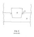
- FIGS. 1 through 4a conventional STI fabrication technique is illustrated in FIGS. 1 through 4 , wherein similar features are denoted by similar reference characters.
- a pad oxide 11is formed over an upper surface of a semiconductor substrate 10 , and a silicon nitride polish stop layer 12 is formed thereon, typically at a thickness in excess of 1000 ⁇ .
- a photomask(not shown) is then used to form an opening through the nitride polish stop layer 12 , pad oxide 11 , and a trench 12 is formed in the semiconductor substrate 10 .
- a thermal oxide liner(not shown) is formed in the trench, an insulating material is deposited and planarization implemented, as by CMP, resulting in the intermediate structure illustrated in FIG. 2 , the reference character 20 denoting the oxide fill.
- the nitride polish stop layer 12 and pad oxide layer 11are removed and cleaning steps are performed prior to forming active regions. Such cleaning steps result in the formation of divots 30 as illustrated in FIG. 3 .
- STI divotsare problematic in various respects.
- STI divotsare responsible for high field edge leakage, particularly with shallow source/drain junctions.
- silicide regions 41 formed on shallow source/drain regions 40grow steeply downwards, as illustrated by reference character 42 , below the junction depth formed at a latter stage resulting in high leakage and shorting.
- Segregation of dopants, notably boron, at STI field edgesreduces the junction depth. Accordingly, after the junctions are silicided, the silicide 42 penetrating to the substrate causes shorting routes and, hence, large leakage occurrence from the source/drain junctions to a well or substrate.
- a parasitic transistor with a low threshold voltageis formed over the area with low impurity concentration causing a kink in the characteristics curve of a transistor.
- the presence of a kinkresults in electrical characteristics different from the design electrical characteristics, thereby preventing the fabrication of transistors with uniform characteristics.
- An advantage of the present inventionis a method of manufacturing a semiconductor device comprising highly reliable STI regions with no or substantially reduced divots.
- a method of manufacturing a semiconductor devicecomprising: forming a nitride polish stop layer, at a thickness no greater than 400 ⁇ , over a semiconductor substrate; forming an opening in the nitride polish stop layer and a trench in the substrate; filling the opening with insulating material forming an overburden on the nitride polish stop layer; and polishing to form an upper planar surface stopping on the nitride polish stop layer, thereby forming a shallow trench isolation region.
- Embodiments of the present inventioncomprise forming a pad oxide on an upper surface of the semiconductor device substrate, forming the nitride polish stop layer, e.g., a silicon nitride polish stop layer, at a thickness of 50 ⁇ to 150 ⁇ , e.g., 100 ⁇ , on the pad oxide layer, filling the opening with dielectric insulating material, such as silicon oxide deposited by chemical vapor deposition, and then implementing chemical mechanical polishing (CMP) to effect planarization stopping on the nitride polish stop layer by removing no more than 20 ⁇ of the upper surface of the nitride polish stop layer.
- CMPchemical mechanical polishing
- Embodiments of the present inventionfurther include ion planting impurities through the nitride polish stop layer to form impurity regions in the semiconductor substrate adjacent the shallow trench isolation region, etching to remove part of the upper surface of the insulating material filling the trench so that the upper surface of the insulating material in the trench is substantially coplanar with the upper surface of the semiconductor substrate, and then removing the nitride polish stop layer. Subsequently, a gate oxide layer is formed on the substrate and a gate electrode layer is formed thereon, employing conventional techniques.
- FIGS. 1 through 4schematically illustrate sequential phases of a conventional method for forming STI regions.
- similar featuresare denoted by similar reference characters.
- FIGS. 5 through 11schematically illustrate sequential phases of a method in accordance with an embodiment of the present invention.
- similar featuresare denoted by similar reference characters.
- the present inventionaddresses and solves problems attendant upon implementing conventional STI methodology resulting in the formation of divots at the corners of an STI region.
- Such conventional methodologytypically comprises forming a relatively thick nitride polish stop layer, as at a thickness greater than 1000 ⁇ .
- Such a thick nitride polish stop layeris typically removed immediately following the STI oxide polish, because subsequent steps require ion implanting to form the active areas, and thick nitride films block such ion implantation.
- Many masking, implanting and cleaning stepsare used to form the active regions resulting in the formation of divots at the corners of the STI region.
- Conventional approaches to this problemseek to minimize these divots as, for example, by optimizing post oxide polish cleans and nitride pull-back prior to STI oxide fill. However, such approaches have not adequately resolved the STI divot problem.
- an extremely thin nitride polish stop layere.g., silicon nitride
- a thickness no greater than 400 ⁇such as at a thickness of 10 ⁇ to 400 ⁇ .
- Suitable silicon nitride polish etch stop layer thicknessesare 50 ⁇ to 150 ⁇ , e.g., 100 ⁇ .
- the thin nitride polish stop layeris not removed immediately after the STI oxide polish. Rather, the thin nitride etch stop layer is retained during subsequent processing comprising masking, ion implanting and cleaning steps to form the active areas.
- the use of a thin nitride etch stop layeris sufficient to protect the filled trench corners, thereby preventing isotropic attack of the oxide at the STI corners, which would otherwise result in the formation of divots.
- the nitride polish stop layeris thin, ion implantation is not blocked.
- the use of a thin nitride polish stop layerpresents a more consistent surface for implantation, because a relatively bare silicon surface rapidly forms an inconsistent native oxide; whereas, the nitride surface is considerably more stable.
- the nitride polish stop layeris retained in place up to the formation of the gate oxide, thereby protecting the active silicon area, providing a much more planar surface and preventing or substantially reducing divots.
- FIGS. 5 through 11A method in accordance with an embodiment of the present invention is schematically illustrated in FIGS. 5 through 11 , wherein similar features are denoted by similar reference characters.
- a pad oxideas at a thickness of 50 ⁇ to 200 ⁇ , e.g., 150 ⁇ , is formed over an upper surface of semiconductor substrate 50 .
- a very thin silicon nitride etch stop layer 52is formed on pad oxide 51 .
- Silicon nitride etch stop layer 52is typically formed at a thickness of 50 ⁇ to 150 ⁇ , e.g., 100 ⁇ .
- a trench 53is then formed in the substrate 50 , as by employing conventional photolithographic and etching techniques.
- a thin thermal oxidemay be formed lining the trench.
- an insulating material 60such as silicon oxide, is deposited to fill the trench and form an overburden on the silicon nitride polish stop layer 52 , as by CVD.
- Planarizationis then implemented, as by CMP, resulting in the intermediate structure illustrated in FIG. 7 , wherein reference character 70 denotes the STI oxide fill.
- CMPis typically conducted such that when stopping on the silicon nitride polish stop layer 52 , no more than 20 ⁇ is removed from the upper surface of silicon nitride polish stop layer 52 .
- the silicon nitride polish stop layeris removed after CMP followed by conventional masking, ion implanting and cleaning steps to form the active regions, resulting in the formation of divots.
- the relatively thin silicon nitride polish stop layer 52is retained during subsequent masking, ion implanting and cleaning steps, which are implemented in a conventional manner, resulting in the formation of impurity regions 80 , as shown in FIG. 8 , which may ultimately be used for source/drain regions of transistors.
- silicon nitride polish stop layer 52is relatively thin, there is virtually little blocking of the ions during implantation.
- the silicon nitride layerforms a stable surface enabling greater uniformity in the formation of the impurity regions.
- the upper surface of the STI oxide fill 70is removed, as by employing hydrofluoric acid, such that the upper surface 70 A is substantially coplanar with the upper surface of semiconductor substrate 50 , resulting in the intermediate structure illustrated in FIG. 9 .
- the silicon nitride polish stop layer 52is removed, as by employing hydrofluoric acid, and the pad oxide layer 51 is then removed, resulting in the structure illustrated in FIG. 10 .
- Subsequent processingis implemented to form a transistor structure as illustrated in FIG. 11 , comprising gate electrode 100 overlying semiconductor substrate 50 with gate oxide 101 therebetween, and dielectric sidewall spaces 102 thereon.
- reference 103represents an interlayer dielectric and element 50 represents an electric contact through the dielectric layer to an active region 80 on substrate 50 .
- Embodiments of the present inventionprovide methodology enabling the fabrication of semiconductor devices with highly reliable STI regions without or with substantially reduced divot formation.
- Embodiments of the present inventioncomprise strategically reducing the thickness of a silicon nitride polish stop layer to below 400 ⁇ and retaining the silicon nitride polish stop layer immediately after CMP to protect the trench corners from isotropic etching during conventional cleaning steps implemented when forming active regions and by retaining the thin silicon nitride polish stop layer during ion implantation, thereby achieving highly uniform implanted regions.
- the present inventionenjoys industrial applicability in fabricating highly integrated semiconductor devices containing STI regions with no or substantially reduced divot formation.
- the present inventionenjoys particular applicability in manufacturing semiconductor devices with sub-micron dimensions.
Landscapes
- Engineering & Computer Science (AREA)
- Physics & Mathematics (AREA)
- Condensed Matter Physics & Semiconductors (AREA)
- General Physics & Mathematics (AREA)
- Manufacturing & Machinery (AREA)
- Computer Hardware Design (AREA)
- Microelectronics & Electronic Packaging (AREA)
- Power Engineering (AREA)
- Element Separation (AREA)
- Insulated Gate Type Field-Effect Transistor (AREA)
Abstract
Description
Claims (7)
Priority Applications (8)
| Application Number | Priority Date | Filing Date | Title |
|---|---|---|---|
| US10/791,759US7091106B2 (en) | 2004-03-04 | 2004-03-04 | Method of reducing STI divot formation during semiconductor device fabrication |
| DE112005000512TDE112005000512B4 (en) | 2004-03-04 | 2005-02-26 | A method of fabricating a semiconductor device having shallow trenches and reduced indentation |
| KR1020067017589AKR20060129037A (en) | 2004-03-04 | 2005-02-26 | How to reduce STi-Divot formation during semiconductor manufacturing |
| JP2007501861AJP2007526652A (en) | 2004-03-04 | 2005-02-26 | Method for reducing STI divot formation during semiconductor device manufacturing |
| CN2005800068145ACN1926679B (en) | 2004-03-04 | 2005-02-26 | Method for reducing shallow trench isolation recess formation in semiconductor device fabrication |
| GB0617207AGB2426126B (en) | 2004-03-04 | 2005-02-26 | Method of reducing STI divot formation during semiconductor device fabrication |
| PCT/US2005/006177WO2005093825A1 (en) | 2004-03-04 | 2005-02-26 | Method of reducing sti divot formation during semiconductor device fabrication |
| TW094106204ATWI355678B (en) | 2004-03-04 | 2005-03-02 | Method of reducing sti divot formation during semi |
Applications Claiming Priority (1)
| Application Number | Priority Date | Filing Date | Title |
|---|---|---|---|
| US10/791,759US7091106B2 (en) | 2004-03-04 | 2004-03-04 | Method of reducing STI divot formation during semiconductor device fabrication |
Publications (2)
| Publication Number | Publication Date |
|---|---|
| US20050196928A1 US20050196928A1 (en) | 2005-09-08 |
| US7091106B2true US7091106B2 (en) | 2006-08-15 |
Family
ID=34911706
Family Applications (1)
| Application Number | Title | Priority Date | Filing Date |
|---|---|---|---|
| US10/791,759Expired - LifetimeUS7091106B2 (en) | 2004-03-04 | 2004-03-04 | Method of reducing STI divot formation during semiconductor device fabrication |
Country Status (8)
| Country | Link |
|---|---|
| US (1) | US7091106B2 (en) |
| JP (1) | JP2007526652A (en) |
| KR (1) | KR20060129037A (en) |
| CN (1) | CN1926679B (en) |
| DE (1) | DE112005000512B4 (en) |
| GB (1) | GB2426126B (en) |
| TW (1) | TWI355678B (en) |
| WO (1) | WO2005093825A1 (en) |
Cited By (6)
| Publication number | Priority date | Publication date | Assignee | Title |
|---|---|---|---|---|
| US20090053834A1 (en)* | 2007-08-23 | 2009-02-26 | Vladimir Alexeevich Ukraintsev | Use of scatterometry for in-line detection of poly-si strings left in sti divot after gate etch |
| US20090289309A1 (en)* | 2008-05-21 | 2009-11-26 | Chartered Semiconductor Manufacturing, Ltd. | Method for reducing silicide defects in integrated circuits |
| US8603895B1 (en) | 2012-09-11 | 2013-12-10 | Globalfoundries Inc. | Methods of forming isolation structures for semiconductor devices by performing a deposition-etch-deposition sequence |
| US9219059B2 (en) | 2012-09-26 | 2015-12-22 | International Business Machines Corporation | Semiconductor structure with integrated passive structures |
| US20160163875A1 (en)* | 2012-06-29 | 2016-06-09 | Taiwan Semiconductor Manufacturing Company, Ltd. | Silicide Process Using OD Spacers |
| US9368386B2 (en) | 2011-05-20 | 2016-06-14 | Globalfoundries Singapore Pte. Ltd. | Corner transistor suppression |
Families Citing this family (14)
| Publication number | Priority date | Publication date | Assignee | Title |
|---|---|---|---|---|
| KR100568259B1 (en)* | 2004-12-14 | 2006-04-07 | 삼성전자주식회사 | Trench isolation semiconductor device and method of forming the same |
| US20080204580A1 (en)* | 2007-02-28 | 2008-08-28 | Micron Technology, Inc. | Method, apparatus and system providing imaging device with color filter array |
| KR100880227B1 (en)* | 2007-10-09 | 2009-01-28 | 주식회사 동부하이텍 | Manufacturing Method of Flash Memory Device |
| WO2010125428A1 (en)* | 2009-04-30 | 2010-11-04 | X-Fab Semiconductor Foundries Ag | Manufacturing integrated circuit components having multiple gate oxidations |
| US8274114B2 (en)* | 2010-01-14 | 2012-09-25 | Broadcom Corporation | Semiconductor device having a modified shallow trench isolation (STI) region and a modified well region |
| US8283722B2 (en) | 2010-06-14 | 2012-10-09 | Broadcom Corporation | Semiconductor device having an enhanced well region |
| US9123807B2 (en) | 2010-12-28 | 2015-09-01 | Broadcom Corporation | Reduction of parasitic capacitance in a semiconductor device |
| US8716102B2 (en)* | 2012-08-14 | 2014-05-06 | Globalfoundries Inc. | Methods of forming isolation structures for semiconductor devices by performing a dry chemical removal process |
| JP6591347B2 (en) | 2016-06-03 | 2019-10-16 | ルネサスエレクトロニクス株式会社 | Manufacturing method of semiconductor device |
| JP6629159B2 (en)* | 2016-09-16 | 2020-01-15 | ルネサスエレクトロニクス株式会社 | Method for manufacturing semiconductor device |
| CN111341724B (en)* | 2018-12-19 | 2022-11-04 | 上海新微技术研发中心有限公司 | Shallow trench isolation process and shallow trench isolation structure |
| KR102821368B1 (en)* | 2019-06-21 | 2025-06-17 | 삼성전자주식회사 | Semiconductor device and method of fabricating the same |
| US12002707B2 (en) | 2020-08-06 | 2024-06-04 | Changxin Memory Technologies, Inc. | Semiconductor structure and manufacturing method thereof |
| CN113611604A (en)* | 2021-03-19 | 2021-11-05 | 联芯集成电路制造(厦门)有限公司 | Method for manufacturing semiconductor element |
Citations (7)
| Publication number | Priority date | Publication date | Assignee | Title |
|---|---|---|---|---|
| US5177028A (en) | 1991-10-22 | 1993-01-05 | Micron Technology, Inc. | Trench isolation method having a double polysilicon gate formed on mesas |
| US5665633A (en)* | 1995-04-06 | 1997-09-09 | Motorola, Inc. | Process for forming a semiconductor device having field isolation |
| US6248641B1 (en)* | 1999-02-05 | 2001-06-19 | United Microelectronics Corp. | Method of fabricating shallow trench isolation |
| US20020098661A1 (en) | 2001-01-25 | 2002-07-25 | Cha Randall Cher Liang | Simplified method to reduce or eliminate sti oxide divots |
| US6555476B1 (en) | 1997-12-23 | 2003-04-29 | Texas Instruments Incorporated | Silicon carbide as a stop layer in chemical mechanical polishing for isolation dielectric |
| US6599810B1 (en)* | 1998-11-05 | 2003-07-29 | Advanced Micro Devices, Inc. | Shallow trench isolation formation with ion implantation |
| US6673695B1 (en) | 2002-02-01 | 2004-01-06 | Chartered Semiconductor Manufacturing Ltd. | STI scheme to prevent fox recess during pre-CMP HF dip |
Family Cites Families (13)
| Publication number | Priority date | Publication date | Assignee | Title |
|---|---|---|---|---|
| US98661A (en)* | 1870-01-11 | Ikank l | ||
| US5234535A (en)* | 1992-12-10 | 1993-08-10 | International Business Machines Corporation | Method of producing a thin silicon-on-insulator layer |
| US5616513A (en)* | 1995-06-01 | 1997-04-01 | International Business Machines Corporation | Shallow trench isolation with self aligned PSG layer |
| JPH098135A (en)* | 1995-06-26 | 1997-01-10 | Toshiba Corp | Method for manufacturing semiconductor device |
| JP3125719B2 (en)* | 1997-07-28 | 2001-01-22 | 日本電気株式会社 | Semiconductor device and manufacturing method thereof |
| JP3053009B2 (en)* | 1997-09-29 | 2000-06-19 | 日本電気株式会社 | Method for manufacturing semiconductor device |
| CN1219328C (en)* | 1998-02-19 | 2005-09-14 | 国际商业机器公司 | Field effect transistors with improved implants and method for making such transistors |
| JP3178416B2 (en)* | 1998-05-22 | 2001-06-18 | 日本電気株式会社 | Method for manufacturing semiconductor device |
| JP2001185731A (en)* | 1999-12-24 | 2001-07-06 | Toshiba Corp | Semiconductor device and manufacturing method thereof |
| KR100346842B1 (en)* | 2000-12-01 | 2002-08-03 | 삼성전자 주식회사 | Semiconductor device having shallow trench isolation structure and method for manufacturing the same |
| US20020142531A1 (en)* | 2001-03-29 | 2002-10-03 | Hsu Sheng Teng | Dual damascene copper gate and interconnect therefore |
| JP4318892B2 (en)* | 2002-05-30 | 2009-08-26 | 富士通マイクロエレクトロニクス株式会社 | Electronic device design method and manufacturing method |
| US6566215B1 (en)* | 2002-06-06 | 2003-05-20 | Chartered Semiconductor Manufacturing Ltd. | Method of fabricating short channel MOS transistors with source/drain extensions |
- 2004
- 2004-03-04USUS10/791,759patent/US7091106B2/ennot_activeExpired - Lifetime
- 2005
- 2005-02-26GBGB0617207Apatent/GB2426126B/ennot_activeExpired - Fee Related
- 2005-02-26KRKR1020067017589Apatent/KR20060129037A/ennot_activeCeased
- 2005-02-26WOPCT/US2005/006177patent/WO2005093825A1/enactiveApplication Filing
- 2005-02-26DEDE112005000512Tpatent/DE112005000512B4/ennot_activeExpired - Fee Related
- 2005-02-26CNCN2005800068145Apatent/CN1926679B/ennot_activeExpired - Fee Related
- 2005-02-26JPJP2007501861Apatent/JP2007526652A/enactivePending
- 2005-03-02TWTW094106204Apatent/TWI355678B/ennot_activeIP Right Cessation
Patent Citations (7)
| Publication number | Priority date | Publication date | Assignee | Title |
|---|---|---|---|---|
| US5177028A (en) | 1991-10-22 | 1993-01-05 | Micron Technology, Inc. | Trench isolation method having a double polysilicon gate formed on mesas |
| US5665633A (en)* | 1995-04-06 | 1997-09-09 | Motorola, Inc. | Process for forming a semiconductor device having field isolation |
| US6555476B1 (en) | 1997-12-23 | 2003-04-29 | Texas Instruments Incorporated | Silicon carbide as a stop layer in chemical mechanical polishing for isolation dielectric |
| US6599810B1 (en)* | 1998-11-05 | 2003-07-29 | Advanced Micro Devices, Inc. | Shallow trench isolation formation with ion implantation |
| US6248641B1 (en)* | 1999-02-05 | 2001-06-19 | United Microelectronics Corp. | Method of fabricating shallow trench isolation |
| US20020098661A1 (en) | 2001-01-25 | 2002-07-25 | Cha Randall Cher Liang | Simplified method to reduce or eliminate sti oxide divots |
| US6673695B1 (en) | 2002-02-01 | 2004-01-06 | Chartered Semiconductor Manufacturing Ltd. | STI scheme to prevent fox recess during pre-CMP HF dip |
Cited By (18)
| Publication number | Priority date | Publication date | Assignee | Title |
|---|---|---|---|---|
| US20090053834A1 (en)* | 2007-08-23 | 2009-02-26 | Vladimir Alexeevich Ukraintsev | Use of scatterometry for in-line detection of poly-si strings left in sti divot after gate etch |
| US20090289309A1 (en)* | 2008-05-21 | 2009-11-26 | Chartered Semiconductor Manufacturing, Ltd. | Method for reducing silicide defects in integrated circuits |
| US7745320B2 (en) | 2008-05-21 | 2010-06-29 | Chartered Semiconductor Manufacturing, Ltd. | Method for reducing silicide defects in integrated circuits |
| US20100267236A1 (en)* | 2008-05-21 | 2010-10-21 | Globalfoundries Singapore Pte. Ltd. | Method for reducing silicide defects in integrated circuits |
| US7960283B2 (en) | 2008-05-21 | 2011-06-14 | Chartered Semiconductor Manufacturing, Ltd. | Method for reducing silicide defects in integrated circuits |
| US9368386B2 (en) | 2011-05-20 | 2016-06-14 | Globalfoundries Singapore Pte. Ltd. | Corner transistor suppression |
| US9905642B2 (en) | 2011-05-20 | 2018-02-27 | Globalfoundries Singapore Pte. Ltd. | Corner transistor suppression |
| US20160163875A1 (en)* | 2012-06-29 | 2016-06-09 | Taiwan Semiconductor Manufacturing Company, Ltd. | Silicide Process Using OD Spacers |
| US9711657B2 (en)* | 2012-06-29 | 2017-07-18 | Taiwan Semiconductor Manufacturing Company, Ltd. | Silicide process using OD spacers |
| US8603895B1 (en) | 2012-09-11 | 2013-12-10 | Globalfoundries Inc. | Methods of forming isolation structures for semiconductor devices by performing a deposition-etch-deposition sequence |
| US9219059B2 (en) | 2012-09-26 | 2015-12-22 | International Business Machines Corporation | Semiconductor structure with integrated passive structures |
| US9425079B2 (en) | 2012-09-26 | 2016-08-23 | International Business Machines Corporation | Semiconductor structure with integrated passive structures |
| US9659961B2 (en) | 2012-09-26 | 2017-05-23 | International Business Machines Corporation | Semiconductor structure with integrated passive structures |
| US9698159B2 (en) | 2012-09-26 | 2017-07-04 | International Business Machines Corporation | Semiconductor structure with integrated passive structures |
| US9768195B2 (en) | 2012-09-26 | 2017-09-19 | International Business Machines Corporation | Semiconductor structure with integrated passive structures |
| US10032862B2 (en) | 2012-09-26 | 2018-07-24 | International Business Machines Corporation | Semiconductor structure with integrated passive structures |
| US10242906B2 (en) | 2012-09-26 | 2019-03-26 | International Business Machines Corporation | Semiconductor structure with integrated passive structures |
| US10580686B2 (en) | 2012-09-26 | 2020-03-03 | International Business Machines Corporation | Semiconductor structure with integrated passive structures |
Also Published As
| Publication number | Publication date |
|---|---|
| JP2007526652A (en) | 2007-09-13 |
| US20050196928A1 (en) | 2005-09-08 |
| GB2426126A (en) | 2006-11-15 |
| DE112005000512B4 (en) | 2011-09-08 |
| KR20060129037A (en) | 2006-12-14 |
| CN1926679B (en) | 2010-10-06 |
| TWI355678B (en) | 2012-01-01 |
| TW200535945A (en) | 2005-11-01 |
| CN1926679A (en) | 2007-03-07 |
| GB0617207D0 (en) | 2006-10-11 |
| GB2426126B (en) | 2008-07-23 |
| WO2005093825A1 (en) | 2005-10-06 |
| DE112005000512T5 (en) | 2007-01-11 |
Similar Documents
| Publication | Publication Date | Title |
|---|---|---|
| US7091106B2 (en) | Method of reducing STI divot formation during semiconductor device fabrication | |
| US6420250B1 (en) | Methods of forming portions of transistor structures, methods of forming array peripheral circuitry, and structures comprising transistor gates | |
| US5777370A (en) | Trench isolation of field effect transistors | |
| US20040021197A1 (en) | Integrated circuits having adjacent P-type doped regions having shallow trench isolation structures without liner layers therein therebetween | |
| US8546268B2 (en) | Manufacturing integrated circuit components having multiple gate oxidations | |
| US6962862B2 (en) | Manufacturing method of semiconductor device | |
| US6326272B1 (en) | Method for forming self-aligned elevated transistor | |
| JPH11145273A (en) | Method for manufacturing semiconductor device | |
| JPH10326891A (en) | Semiconductor device and manufacturing method thereof | |
| KR20010025030A (en) | Method of manufacturing a mis field-effect transistor | |
| US20070066000A1 (en) | Method of manufacturing a semiconductor device | |
| US6150237A (en) | Method of fabricating STI | |
| US5972777A (en) | Method of forming isolation by nitrogen implant to reduce bird's beak | |
| JP2006313901A (en) | Semiconductor device and method for manufacturing semiconductor device | |
| US20060081903A1 (en) | Semiconductor device and method of fabricating the same | |
| US11640979B2 (en) | Method of manufacturing semiconductor device | |
| JPH06232253A (en) | Element-isolation method of semiconductor device | |
| US7361571B2 (en) | Method for fabricating a trench isolation with spacers | |
| US6323112B1 (en) | Method of fabricating integrated circuits | |
| US7022583B1 (en) | Method of forming a shallow trench isolation device to prevent kick effect | |
| US6344374B1 (en) | Method of fabricating insulators for isolating electronic devices | |
| US7144785B2 (en) | Method of forming isolation trench with spacer formation | |
| US6773975B1 (en) | Formation of a shallow trench isolation structure in integrated circuits | |
| US7223698B1 (en) | Method of forming a semiconductor arrangement with reduced field-to active step height | |
| JP4989076B2 (en) | Manufacturing method of semiconductor device |
Legal Events
| Date | Code | Title | Description |
|---|---|---|---|
| AS | Assignment | Owner name:ADVANCED MICRO DEVICES, INC., CALIFORNIA Free format text:ASSIGNMENT OF ASSIGNORS INTEREST;ASSIGNORS:BONSER, DOUGLAS J.;GROSCHOPF, JOHANNES F.;DAKSHINA-MURTHY, SRIKANTESWARA;AND OTHERS;REEL/FRAME:015049/0174;SIGNING DATES FROM 20040204 TO 20040205 | |
| STCF | Information on status: patent grant | Free format text:PATENTED CASE | |
| AS | Assignment | Owner name:GLOBALFOUNDRIES INC., CAYMAN ISLANDS Free format text:AFFIRMATION OF PATENT ASSIGNMENT;ASSIGNOR:ADVANCED MICRO DEVICES, INC.;REEL/FRAME:023119/0083 Effective date:20090630 | |
| FPAY | Fee payment | Year of fee payment:4 | |
| FPAY | Fee payment | Year of fee payment:8 | |
| MAFP | Maintenance fee payment | Free format text:PAYMENT OF MAINTENANCE FEE, 12TH YEAR, LARGE ENTITY (ORIGINAL EVENT CODE: M1553) Year of fee payment:12 | |
| AS | Assignment | Owner name:WILMINGTON TRUST, NATIONAL ASSOCIATION, DELAWARE Free format text:SECURITY AGREEMENT;ASSIGNOR:GLOBALFOUNDRIES INC.;REEL/FRAME:049490/0001 Effective date:20181127 | |
| AS | Assignment | Owner name:GLOBALFOUNDRIES U.S. INC., CALIFORNIA Free format text:ASSIGNMENT OF ASSIGNORS INTEREST;ASSIGNOR:GLOBALFOUNDRIES INC.;REEL/FRAME:054633/0001 Effective date:20201022 | |
| AS | Assignment | Owner name:GLOBALFOUNDRIES INC., CAYMAN ISLANDS Free format text:RELEASE BY SECURED PARTY;ASSIGNOR:WILMINGTON TRUST, NATIONAL ASSOCIATION;REEL/FRAME:054636/0001 Effective date:20201117 | |
| AS | Assignment | Owner name:GLOBALFOUNDRIES U.S. INC., NEW YORK Free format text:RELEASE BY SECURED PARTY;ASSIGNOR:WILMINGTON TRUST, NATIONAL ASSOCIATION;REEL/FRAME:056987/0001 Effective date:20201117 |