US7091064B2 - Method and apparatus for attaching microelectronic substrates and support members - Google Patents
Method and apparatus for attaching microelectronic substrates and support membersDownload PDFInfo
- Publication number
- US7091064B2 US7091064B2US10/926,434US92643404AUS7091064B2US 7091064 B2US7091064 B2US 7091064B2US 92643404 AUS92643404 AUS 92643404AUS 7091064 B2US7091064 B2US 7091064B2
- Authority
- US
- United States
- Prior art keywords
- support member
- microelectronic substrate
- disposing
- attachment structure
- partially
- Prior art date
- Legal status (The legal status is an assumption and is not a legal conclusion. Google has not performed a legal analysis and makes no representation as to the accuracy of the status listed.)
- Expired - Fee Related
Links
Images


Classifications
- H—ELECTRICITY
- H01—ELECTRIC ELEMENTS
- H01L—SEMICONDUCTOR DEVICES NOT COVERED BY CLASS H10
- H01L23/00—Details of semiconductor or other solid state devices
- H01L23/12—Mountings, e.g. non-detachable insulating substrates
- H01L23/13—Mountings, e.g. non-detachable insulating substrates characterised by the shape
- H—ELECTRICITY
- H01—ELECTRIC ELEMENTS
- H01L—SEMICONDUCTOR DEVICES NOT COVERED BY CLASS H10
- H01L23/00—Details of semiconductor or other solid state devices
- H01L23/28—Encapsulations, e.g. encapsulating layers, coatings, e.g. for protection
- H01L23/31—Encapsulations, e.g. encapsulating layers, coatings, e.g. for protection characterised by the arrangement or shape
- H01L23/3107—Encapsulations, e.g. encapsulating layers, coatings, e.g. for protection characterised by the arrangement or shape the device being completely enclosed
- H01L23/3121—Encapsulations, e.g. encapsulating layers, coatings, e.g. for protection characterised by the arrangement or shape the device being completely enclosed a substrate forming part of the encapsulation
- H—ELECTRICITY
- H01—ELECTRIC ELEMENTS
- H01L—SEMICONDUCTOR DEVICES NOT COVERED BY CLASS H10
- H01L23/00—Details of semiconductor or other solid state devices
- H01L23/48—Arrangements for conducting electric current to or from the solid state body in operation, e.g. leads, terminal arrangements ; Selection of materials therefor
- H01L23/488—Arrangements for conducting electric current to or from the solid state body in operation, e.g. leads, terminal arrangements ; Selection of materials therefor consisting of soldered or bonded constructions
- H01L23/495—Lead-frames or other flat leads
- H01L23/49503—Lead-frames or other flat leads characterised by the die pad
- H01L23/4951—Chip-on-leads or leads-on-chip techniques, i.e. inner lead fingers being used as die pad
- H—ELECTRICITY
- H01—ELECTRIC ELEMENTS
- H01L—SEMICONDUCTOR DEVICES NOT COVERED BY CLASS H10
- H01L23/00—Details of semiconductor or other solid state devices
- H01L23/48—Arrangements for conducting electric current to or from the solid state body in operation, e.g. leads, terminal arrangements ; Selection of materials therefor
- H01L23/488—Arrangements for conducting electric current to or from the solid state body in operation, e.g. leads, terminal arrangements ; Selection of materials therefor consisting of soldered or bonded constructions
- H01L23/495—Lead-frames or other flat leads
- H01L23/49503—Lead-frames or other flat leads characterised by the die pad
- H01L23/49513—Lead-frames or other flat leads characterised by the die pad having bonding material between chip and die pad
- H—ELECTRICITY
- H01—ELECTRIC ELEMENTS
- H01L—SEMICONDUCTOR DEVICES NOT COVERED BY CLASS H10
- H01L23/00—Details of semiconductor or other solid state devices
- H01L23/48—Arrangements for conducting electric current to or from the solid state body in operation, e.g. leads, terminal arrangements ; Selection of materials therefor
- H01L23/488—Arrangements for conducting electric current to or from the solid state body in operation, e.g. leads, terminal arrangements ; Selection of materials therefor consisting of soldered or bonded constructions
- H01L23/498—Leads, i.e. metallisations or lead-frames on insulating substrates, e.g. chip carriers
- H01L23/49827—Via connections through the substrates, e.g. pins going through the substrate, coaxial cables
- H—ELECTRICITY
- H01—ELECTRIC ELEMENTS
- H01L—SEMICONDUCTOR DEVICES NOT COVERED BY CLASS H10
- H01L24/00—Arrangements for connecting or disconnecting semiconductor or solid-state bodies; Methods or apparatus related thereto
- H01L24/01—Means for bonding being attached to, or being formed on, the surface to be connected, e.g. chip-to-package, die-attach, "first-level" interconnects; Manufacturing methods related thereto
- H01L24/26—Layer connectors, e.g. plate connectors, solder or adhesive layers; Manufacturing methods related thereto
- H01L24/28—Structure, shape, material or disposition of the layer connectors prior to the connecting process
- H01L24/29—Structure, shape, material or disposition of the layer connectors prior to the connecting process of an individual layer connector
- H—ELECTRICITY
- H01—ELECTRIC ELEMENTS
- H01L—SEMICONDUCTOR DEVICES NOT COVERED BY CLASS H10
- H01L24/00—Arrangements for connecting or disconnecting semiconductor or solid-state bodies; Methods or apparatus related thereto
- H01L24/01—Means for bonding being attached to, or being formed on, the surface to be connected, e.g. chip-to-package, die-attach, "first-level" interconnects; Manufacturing methods related thereto
- H01L24/26—Layer connectors, e.g. plate connectors, solder or adhesive layers; Manufacturing methods related thereto
- H01L24/31—Structure, shape, material or disposition of the layer connectors after the connecting process
- H01L24/32—Structure, shape, material or disposition of the layer connectors after the connecting process of an individual layer connector
- H—ELECTRICITY
- H01—ELECTRIC ELEMENTS
- H01L—SEMICONDUCTOR DEVICES NOT COVERED BY CLASS H10
- H01L24/00—Arrangements for connecting or disconnecting semiconductor or solid-state bodies; Methods or apparatus related thereto
- H01L24/80—Methods for connecting semiconductor or other solid state bodies using means for bonding being attached to, or being formed on, the surface to be connected
- H01L24/83—Methods for connecting semiconductor or other solid state bodies using means for bonding being attached to, or being formed on, the surface to be connected using a layer connector
- H—ELECTRICITY
- H01—ELECTRIC ELEMENTS
- H01L—SEMICONDUCTOR DEVICES NOT COVERED BY CLASS H10
- H01L21/00—Processes or apparatus adapted for the manufacture or treatment of semiconductor or solid state devices or of parts thereof
- H01L21/02—Manufacture or treatment of semiconductor devices or of parts thereof
- H01L21/04—Manufacture or treatment of semiconductor devices or of parts thereof the devices having potential barriers, e.g. a PN junction, depletion layer or carrier concentration layer
- H01L21/48—Manufacture or treatment of parts, e.g. containers, prior to assembly of the devices, using processes not provided for in a single one of the groups H01L21/18 - H01L21/326 or H10D48/04 - H10D48/07
- H01L21/4814—Conductive parts
- H01L21/4846—Leads on or in insulating or insulated substrates, e.g. metallisation
- H01L21/4853—Connection or disconnection of other leads to or from a metallisation, e.g. pins, wires, bumps
- H—ELECTRICITY
- H01—ELECTRIC ELEMENTS
- H01L—SEMICONDUCTOR DEVICES NOT COVERED BY CLASS H10
- H01L2224/00—Indexing scheme for arrangements for connecting or disconnecting semiconductor or solid-state bodies and methods related thereto as covered by H01L24/00
- H01L2224/01—Means for bonding being attached to, or being formed on, the surface to be connected, e.g. chip-to-package, die-attach, "first-level" interconnects; Manufacturing methods related thereto
- H01L2224/02—Bonding areas; Manufacturing methods related thereto
- H01L2224/04—Structure, shape, material or disposition of the bonding areas prior to the connecting process
- H01L2224/05—Structure, shape, material or disposition of the bonding areas prior to the connecting process of an individual bonding area
- H01L2224/0554—External layer
- H01L2224/05599—Material
- H—ELECTRICITY
- H01—ELECTRIC ELEMENTS
- H01L—SEMICONDUCTOR DEVICES NOT COVERED BY CLASS H10
- H01L2224/00—Indexing scheme for arrangements for connecting or disconnecting semiconductor or solid-state bodies and methods related thereto as covered by H01L24/00
- H01L2224/01—Means for bonding being attached to, or being formed on, the surface to be connected, e.g. chip-to-package, die-attach, "first-level" interconnects; Manufacturing methods related thereto
- H01L2224/02—Bonding areas; Manufacturing methods related thereto
- H01L2224/04—Structure, shape, material or disposition of the bonding areas prior to the connecting process
- H01L2224/06—Structure, shape, material or disposition of the bonding areas prior to the connecting process of a plurality of bonding areas
- H01L2224/061—Disposition
- H01L2224/0612—Layout
- H01L2224/0613—Square or rectangular array
- H01L2224/06134—Square or rectangular array covering only portions of the surface to be connected
- H01L2224/06136—Covering only the central area of the surface to be connected, i.e. central arrangements
- H—ELECTRICITY
- H01—ELECTRIC ELEMENTS
- H01L—SEMICONDUCTOR DEVICES NOT COVERED BY CLASS H10
- H01L2224/00—Indexing scheme for arrangements for connecting or disconnecting semiconductor or solid-state bodies and methods related thereto as covered by H01L24/00
- H01L2224/01—Means for bonding being attached to, or being formed on, the surface to be connected, e.g. chip-to-package, die-attach, "first-level" interconnects; Manufacturing methods related thereto
- H01L2224/26—Layer connectors, e.g. plate connectors, solder or adhesive layers; Manufacturing methods related thereto
- H01L2224/28—Structure, shape, material or disposition of the layer connectors prior to the connecting process
- H01L2224/29—Structure, shape, material or disposition of the layer connectors prior to the connecting process of an individual layer connector
- H01L2224/29001—Core members of the layer connector
- H01L2224/29005—Structure
- H01L2224/29007—Layer connector smaller than the underlying bonding area
- H—ELECTRICITY
- H01—ELECTRIC ELEMENTS
- H01L—SEMICONDUCTOR DEVICES NOT COVERED BY CLASS H10
- H01L2224/00—Indexing scheme for arrangements for connecting or disconnecting semiconductor or solid-state bodies and methods related thereto as covered by H01L24/00
- H01L2224/01—Means for bonding being attached to, or being formed on, the surface to be connected, e.g. chip-to-package, die-attach, "first-level" interconnects; Manufacturing methods related thereto
- H01L2224/26—Layer connectors, e.g. plate connectors, solder or adhesive layers; Manufacturing methods related thereto
- H01L2224/28—Structure, shape, material or disposition of the layer connectors prior to the connecting process
- H01L2224/29—Structure, shape, material or disposition of the layer connectors prior to the connecting process of an individual layer connector
- H01L2224/29001—Core members of the layer connector
- H01L2224/29099—Material
- H01L2224/291—Material with a principal constituent of the material being a metal or a metalloid, e.g. boron [B], silicon [Si], germanium [Ge], arsenic [As], antimony [Sb], tellurium [Te] and polonium [Po], and alloys thereof
- H01L2224/29101—Material with a principal constituent of the material being a metal or a metalloid, e.g. boron [B], silicon [Si], germanium [Ge], arsenic [As], antimony [Sb], tellurium [Te] and polonium [Po], and alloys thereof the principal constituent melting at a temperature of less than 400°C
- H—ELECTRICITY
- H01—ELECTRIC ELEMENTS
- H01L—SEMICONDUCTOR DEVICES NOT COVERED BY CLASS H10
- H01L2224/00—Indexing scheme for arrangements for connecting or disconnecting semiconductor or solid-state bodies and methods related thereto as covered by H01L24/00
- H01L2224/01—Means for bonding being attached to, or being formed on, the surface to be connected, e.g. chip-to-package, die-attach, "first-level" interconnects; Manufacturing methods related thereto
- H01L2224/26—Layer connectors, e.g. plate connectors, solder or adhesive layers; Manufacturing methods related thereto
- H01L2224/28—Structure, shape, material or disposition of the layer connectors prior to the connecting process
- H01L2224/29—Structure, shape, material or disposition of the layer connectors prior to the connecting process of an individual layer connector
- H01L2224/29001—Core members of the layer connector
- H01L2224/29099—Material
- H01L2224/2919—Material with a principal constituent of the material being a polymer, e.g. polyester, phenolic based polymer, epoxy
- H—ELECTRICITY
- H01—ELECTRIC ELEMENTS
- H01L—SEMICONDUCTOR DEVICES NOT COVERED BY CLASS H10
- H01L2224/00—Indexing scheme for arrangements for connecting or disconnecting semiconductor or solid-state bodies and methods related thereto as covered by H01L24/00
- H01L2224/01—Means for bonding being attached to, or being formed on, the surface to be connected, e.g. chip-to-package, die-attach, "first-level" interconnects; Manufacturing methods related thereto
- H01L2224/26—Layer connectors, e.g. plate connectors, solder or adhesive layers; Manufacturing methods related thereto
- H01L2224/28—Structure, shape, material or disposition of the layer connectors prior to the connecting process
- H01L2224/29—Structure, shape, material or disposition of the layer connectors prior to the connecting process of an individual layer connector
- H01L2224/29001—Core members of the layer connector
- H01L2224/29099—Material
- H01L2224/29198—Material with a principal constituent of the material being a combination of two or more materials in the form of a matrix with a filler, i.e. being a hybrid material, e.g. segmented structures, foams
- H01L2224/29298—Fillers
- H—ELECTRICITY
- H01—ELECTRIC ELEMENTS
- H01L—SEMICONDUCTOR DEVICES NOT COVERED BY CLASS H10
- H01L2224/00—Indexing scheme for arrangements for connecting or disconnecting semiconductor or solid-state bodies and methods related thereto as covered by H01L24/00
- H01L2224/01—Means for bonding being attached to, or being formed on, the surface to be connected, e.g. chip-to-package, die-attach, "first-level" interconnects; Manufacturing methods related thereto
- H01L2224/26—Layer connectors, e.g. plate connectors, solder or adhesive layers; Manufacturing methods related thereto
- H01L2224/31—Structure, shape, material or disposition of the layer connectors after the connecting process
- H01L2224/32—Structure, shape, material or disposition of the layer connectors after the connecting process of an individual layer connector
- H01L2224/321—Disposition
- H01L2224/32151—Disposition the layer connector connecting between a semiconductor or solid-state body and an item not being a semiconductor or solid-state body, e.g. chip-to-substrate, chip-to-passive
- H01L2224/32221—Disposition the layer connector connecting between a semiconductor or solid-state body and an item not being a semiconductor or solid-state body, e.g. chip-to-substrate, chip-to-passive the body and the item being stacked
- H01L2224/32225—Disposition the layer connector connecting between a semiconductor or solid-state body and an item not being a semiconductor or solid-state body, e.g. chip-to-substrate, chip-to-passive the body and the item being stacked the item being non-metallic, e.g. insulating substrate with or without metallisation
- H—ELECTRICITY
- H01—ELECTRIC ELEMENTS
- H01L—SEMICONDUCTOR DEVICES NOT COVERED BY CLASS H10
- H01L2224/00—Indexing scheme for arrangements for connecting or disconnecting semiconductor or solid-state bodies and methods related thereto as covered by H01L24/00
- H01L2224/01—Means for bonding being attached to, or being formed on, the surface to be connected, e.g. chip-to-package, die-attach, "first-level" interconnects; Manufacturing methods related thereto
- H01L2224/26—Layer connectors, e.g. plate connectors, solder or adhesive layers; Manufacturing methods related thereto
- H01L2224/31—Structure, shape, material or disposition of the layer connectors after the connecting process
- H01L2224/32—Structure, shape, material or disposition of the layer connectors after the connecting process of an individual layer connector
- H01L2224/321—Disposition
- H01L2224/32151—Disposition the layer connector connecting between a semiconductor or solid-state body and an item not being a semiconductor or solid-state body, e.g. chip-to-substrate, chip-to-passive
- H01L2224/32221—Disposition the layer connector connecting between a semiconductor or solid-state body and an item not being a semiconductor or solid-state body, e.g. chip-to-substrate, chip-to-passive the body and the item being stacked
- H01L2224/32245—Disposition the layer connector connecting between a semiconductor or solid-state body and an item not being a semiconductor or solid-state body, e.g. chip-to-substrate, chip-to-passive the body and the item being stacked the item being metallic
- H—ELECTRICITY
- H01—ELECTRIC ELEMENTS
- H01L—SEMICONDUCTOR DEVICES NOT COVERED BY CLASS H10
- H01L2224/00—Indexing scheme for arrangements for connecting or disconnecting semiconductor or solid-state bodies and methods related thereto as covered by H01L24/00
- H01L2224/01—Means for bonding being attached to, or being formed on, the surface to be connected, e.g. chip-to-package, die-attach, "first-level" interconnects; Manufacturing methods related thereto
- H01L2224/42—Wire connectors; Manufacturing methods related thereto
- H01L2224/44—Structure, shape, material or disposition of the wire connectors prior to the connecting process
- H01L2224/45—Structure, shape, material or disposition of the wire connectors prior to the connecting process of an individual wire connector
- H01L2224/45001—Core members of the connector
- H01L2224/45099—Material
- H—ELECTRICITY
- H01—ELECTRIC ELEMENTS
- H01L—SEMICONDUCTOR DEVICES NOT COVERED BY CLASS H10
- H01L2224/00—Indexing scheme for arrangements for connecting or disconnecting semiconductor or solid-state bodies and methods related thereto as covered by H01L24/00
- H01L2224/01—Means for bonding being attached to, or being formed on, the surface to be connected, e.g. chip-to-package, die-attach, "first-level" interconnects; Manufacturing methods related thereto
- H01L2224/42—Wire connectors; Manufacturing methods related thereto
- H01L2224/47—Structure, shape, material or disposition of the wire connectors after the connecting process
- H01L2224/48—Structure, shape, material or disposition of the wire connectors after the connecting process of an individual wire connector
- H01L2224/4805—Shape
- H01L2224/4809—Loop shape
- H01L2224/48091—Arched
- H—ELECTRICITY
- H01—ELECTRIC ELEMENTS
- H01L—SEMICONDUCTOR DEVICES NOT COVERED BY CLASS H10
- H01L2224/00—Indexing scheme for arrangements for connecting or disconnecting semiconductor or solid-state bodies and methods related thereto as covered by H01L24/00
- H01L2224/01—Means for bonding being attached to, or being formed on, the surface to be connected, e.g. chip-to-package, die-attach, "first-level" interconnects; Manufacturing methods related thereto
- H01L2224/42—Wire connectors; Manufacturing methods related thereto
- H01L2224/47—Structure, shape, material or disposition of the wire connectors after the connecting process
- H01L2224/48—Structure, shape, material or disposition of the wire connectors after the connecting process of an individual wire connector
- H01L2224/481—Disposition
- H01L2224/48151—Connecting between a semiconductor or solid-state body and an item not being a semiconductor or solid-state body, e.g. chip-to-substrate, chip-to-passive
- H01L2224/48221—Connecting between a semiconductor or solid-state body and an item not being a semiconductor or solid-state body, e.g. chip-to-substrate, chip-to-passive the body and the item being stacked
- H01L2224/48225—Connecting between a semiconductor or solid-state body and an item not being a semiconductor or solid-state body, e.g. chip-to-substrate, chip-to-passive the body and the item being stacked the item being non-metallic, e.g. insulating substrate with or without metallisation
- H01L2224/48227—Connecting between a semiconductor or solid-state body and an item not being a semiconductor or solid-state body, e.g. chip-to-substrate, chip-to-passive the body and the item being stacked the item being non-metallic, e.g. insulating substrate with or without metallisation connecting the wire to a bond pad of the item
- H—ELECTRICITY
- H01—ELECTRIC ELEMENTS
- H01L—SEMICONDUCTOR DEVICES NOT COVERED BY CLASS H10
- H01L2224/00—Indexing scheme for arrangements for connecting or disconnecting semiconductor or solid-state bodies and methods related thereto as covered by H01L24/00
- H01L2224/01—Means for bonding being attached to, or being formed on, the surface to be connected, e.g. chip-to-package, die-attach, "first-level" interconnects; Manufacturing methods related thereto
- H01L2224/42—Wire connectors; Manufacturing methods related thereto
- H01L2224/47—Structure, shape, material or disposition of the wire connectors after the connecting process
- H01L2224/48—Structure, shape, material or disposition of the wire connectors after the connecting process of an individual wire connector
- H01L2224/481—Disposition
- H01L2224/48151—Connecting between a semiconductor or solid-state body and an item not being a semiconductor or solid-state body, e.g. chip-to-substrate, chip-to-passive
- H01L2224/48221—Connecting between a semiconductor or solid-state body and an item not being a semiconductor or solid-state body, e.g. chip-to-substrate, chip-to-passive the body and the item being stacked
- H01L2224/48225—Connecting between a semiconductor or solid-state body and an item not being a semiconductor or solid-state body, e.g. chip-to-substrate, chip-to-passive the body and the item being stacked the item being non-metallic, e.g. insulating substrate with or without metallisation
- H01L2224/4824—Connecting between the body and an opposite side of the item with respect to the body
- H—ELECTRICITY
- H01—ELECTRIC ELEMENTS
- H01L—SEMICONDUCTOR DEVICES NOT COVERED BY CLASS H10
- H01L2224/00—Indexing scheme for arrangements for connecting or disconnecting semiconductor or solid-state bodies and methods related thereto as covered by H01L24/00
- H01L2224/01—Means for bonding being attached to, or being formed on, the surface to be connected, e.g. chip-to-package, die-attach, "first-level" interconnects; Manufacturing methods related thereto
- H01L2224/42—Wire connectors; Manufacturing methods related thereto
- H01L2224/47—Structure, shape, material or disposition of the wire connectors after the connecting process
- H01L2224/48—Structure, shape, material or disposition of the wire connectors after the connecting process of an individual wire connector
- H01L2224/481—Disposition
- H01L2224/48151—Connecting between a semiconductor or solid-state body and an item not being a semiconductor or solid-state body, e.g. chip-to-substrate, chip-to-passive
- H01L2224/48221—Connecting between a semiconductor or solid-state body and an item not being a semiconductor or solid-state body, e.g. chip-to-substrate, chip-to-passive the body and the item being stacked
- H01L2224/48245—Connecting between a semiconductor or solid-state body and an item not being a semiconductor or solid-state body, e.g. chip-to-substrate, chip-to-passive the body and the item being stacked the item being metallic
- H01L2224/48247—Connecting between a semiconductor or solid-state body and an item not being a semiconductor or solid-state body, e.g. chip-to-substrate, chip-to-passive the body and the item being stacked the item being metallic connecting the wire to a bond pad of the item
- H—ELECTRICITY
- H01—ELECTRIC ELEMENTS
- H01L—SEMICONDUCTOR DEVICES NOT COVERED BY CLASS H10
- H01L2224/00—Indexing scheme for arrangements for connecting or disconnecting semiconductor or solid-state bodies and methods related thereto as covered by H01L24/00
- H01L2224/01—Means for bonding being attached to, or being formed on, the surface to be connected, e.g. chip-to-package, die-attach, "first-level" interconnects; Manufacturing methods related thereto
- H01L2224/42—Wire connectors; Manufacturing methods related thereto
- H01L2224/47—Structure, shape, material or disposition of the wire connectors after the connecting process
- H01L2224/48—Structure, shape, material or disposition of the wire connectors after the connecting process of an individual wire connector
- H01L2224/481—Disposition
- H01L2224/48151—Connecting between a semiconductor or solid-state body and an item not being a semiconductor or solid-state body, e.g. chip-to-substrate, chip-to-passive
- H01L2224/48221—Connecting between a semiconductor or solid-state body and an item not being a semiconductor or solid-state body, e.g. chip-to-substrate, chip-to-passive the body and the item being stacked
- H01L2224/48245—Connecting between a semiconductor or solid-state body and an item not being a semiconductor or solid-state body, e.g. chip-to-substrate, chip-to-passive the body and the item being stacked the item being metallic
- H01L2224/4826—Connecting between the body and an opposite side of the item with respect to the body
- H—ELECTRICITY
- H01—ELECTRIC ELEMENTS
- H01L—SEMICONDUCTOR DEVICES NOT COVERED BY CLASS H10
- H01L2224/00—Indexing scheme for arrangements for connecting or disconnecting semiconductor or solid-state bodies and methods related thereto as covered by H01L24/00
- H01L2224/73—Means for bonding being of different types provided for in two or more of groups H01L2224/10, H01L2224/18, H01L2224/26, H01L2224/34, H01L2224/42, H01L2224/50, H01L2224/63, H01L2224/71
- H01L2224/732—Location after the connecting process
- H01L2224/73201—Location after the connecting process on the same surface
- H01L2224/73215—Layer and wire connectors
- H—ELECTRICITY
- H01—ELECTRIC ELEMENTS
- H01L—SEMICONDUCTOR DEVICES NOT COVERED BY CLASS H10
- H01L2224/00—Indexing scheme for arrangements for connecting or disconnecting semiconductor or solid-state bodies and methods related thereto as covered by H01L24/00
- H01L2224/73—Means for bonding being of different types provided for in two or more of groups H01L2224/10, H01L2224/18, H01L2224/26, H01L2224/34, H01L2224/42, H01L2224/50, H01L2224/63, H01L2224/71
- H01L2224/732—Location after the connecting process
- H01L2224/73251—Location after the connecting process on different surfaces
- H01L2224/73265—Layer and wire connectors
- H—ELECTRICITY
- H01—ELECTRIC ELEMENTS
- H01L—SEMICONDUCTOR DEVICES NOT COVERED BY CLASS H10
- H01L2224/00—Indexing scheme for arrangements for connecting or disconnecting semiconductor or solid-state bodies and methods related thereto as covered by H01L24/00
- H01L2224/80—Methods for connecting semiconductor or other solid state bodies using means for bonding being attached to, or being formed on, the surface to be connected
- H01L2224/83—Methods for connecting semiconductor or other solid state bodies using means for bonding being attached to, or being formed on, the surface to be connected using a layer connector
- H01L2224/8319—Arrangement of the layer connectors prior to mounting
- H01L2224/83192—Arrangement of the layer connectors prior to mounting wherein the layer connectors are disposed only on another item or body to be connected to the semiconductor or solid-state body
- H—ELECTRICITY
- H01—ELECTRIC ELEMENTS
- H01L—SEMICONDUCTOR DEVICES NOT COVERED BY CLASS H10
- H01L2224/00—Indexing scheme for arrangements for connecting or disconnecting semiconductor or solid-state bodies and methods related thereto as covered by H01L24/00
- H01L2224/80—Methods for connecting semiconductor or other solid state bodies using means for bonding being attached to, or being formed on, the surface to be connected
- H01L2224/83—Methods for connecting semiconductor or other solid state bodies using means for bonding being attached to, or being formed on, the surface to be connected using a layer connector
- H01L2224/8319—Arrangement of the layer connectors prior to mounting
- H01L2224/83193—Arrangement of the layer connectors prior to mounting wherein the layer connectors are disposed on both the semiconductor or solid-state body and another item or body to be connected to the semiconductor or solid-state body
- H—ELECTRICITY
- H01—ELECTRIC ELEMENTS
- H01L—SEMICONDUCTOR DEVICES NOT COVERED BY CLASS H10
- H01L2224/00—Indexing scheme for arrangements for connecting or disconnecting semiconductor or solid-state bodies and methods related thereto as covered by H01L24/00
- H01L2224/80—Methods for connecting semiconductor or other solid state bodies using means for bonding being attached to, or being formed on, the surface to be connected
- H01L2224/83—Methods for connecting semiconductor or other solid state bodies using means for bonding being attached to, or being formed on, the surface to be connected using a layer connector
- H01L2224/8319—Arrangement of the layer connectors prior to mounting
- H01L2224/83194—Lateral distribution of the layer connectors
- H—ELECTRICITY
- H01—ELECTRIC ELEMENTS
- H01L—SEMICONDUCTOR DEVICES NOT COVERED BY CLASS H10
- H01L2224/00—Indexing scheme for arrangements for connecting or disconnecting semiconductor or solid-state bodies and methods related thereto as covered by H01L24/00
- H01L2224/80—Methods for connecting semiconductor or other solid state bodies using means for bonding being attached to, or being formed on, the surface to be connected
- H01L2224/83—Methods for connecting semiconductor or other solid state bodies using means for bonding being attached to, or being formed on, the surface to be connected using a layer connector
- H01L2224/838—Bonding techniques
- H01L2224/8385—Bonding techniques using a polymer adhesive, e.g. an adhesive based on silicone, epoxy, polyimide, polyester
- H01L2224/83855—Hardening the adhesive by curing, i.e. thermosetting
- H01L2224/83856—Pre-cured adhesive, i.e. B-stage adhesive
- H—ELECTRICITY
- H01—ELECTRIC ELEMENTS
- H01L—SEMICONDUCTOR DEVICES NOT COVERED BY CLASS H10
- H01L2224/00—Indexing scheme for arrangements for connecting or disconnecting semiconductor or solid-state bodies and methods related thereto as covered by H01L24/00
- H01L2224/80—Methods for connecting semiconductor or other solid state bodies using means for bonding being attached to, or being formed on, the surface to be connected
- H01L2224/85—Methods for connecting semiconductor or other solid state bodies using means for bonding being attached to, or being formed on, the surface to be connected using a wire connector
- H01L2224/8538—Bonding interfaces outside the semiconductor or solid-state body
- H01L2224/85399—Material
- H—ELECTRICITY
- H01—ELECTRIC ELEMENTS
- H01L—SEMICONDUCTOR DEVICES NOT COVERED BY CLASS H10
- H01L2224/00—Indexing scheme for arrangements for connecting or disconnecting semiconductor or solid-state bodies and methods related thereto as covered by H01L24/00
- H01L2224/91—Methods for connecting semiconductor or solid state bodies including different methods provided for in two or more of groups H01L2224/80 - H01L2224/90
- H01L2224/92—Specific sequence of method steps
- H01L2224/921—Connecting a surface with connectors of different types
- H01L2224/9212—Sequential connecting processes
- H01L2224/92142—Sequential connecting processes the first connecting process involving a layer connector
- H01L2224/92147—Sequential connecting processes the first connecting process involving a layer connector the second connecting process involving a wire connector
- H—ELECTRICITY
- H01—ELECTRIC ELEMENTS
- H01L—SEMICONDUCTOR DEVICES NOT COVERED BY CLASS H10
- H01L24/00—Arrangements for connecting or disconnecting semiconductor or solid-state bodies; Methods or apparatus related thereto
- H01L24/01—Means for bonding being attached to, or being formed on, the surface to be connected, e.g. chip-to-package, die-attach, "first-level" interconnects; Manufacturing methods related thereto
- H01L24/42—Wire connectors; Manufacturing methods related thereto
- H01L24/47—Structure, shape, material or disposition of the wire connectors after the connecting process
- H01L24/48—Structure, shape, material or disposition of the wire connectors after the connecting process of an individual wire connector
- H—ELECTRICITY
- H01—ELECTRIC ELEMENTS
- H01L—SEMICONDUCTOR DEVICES NOT COVERED BY CLASS H10
- H01L24/00—Arrangements for connecting or disconnecting semiconductor or solid-state bodies; Methods or apparatus related thereto
- H01L24/73—Means for bonding being of different types provided for in two or more of groups H01L24/10, H01L24/18, H01L24/26, H01L24/34, H01L24/42, H01L24/50, H01L24/63, H01L24/71
- H—ELECTRICITY
- H01—ELECTRIC ELEMENTS
- H01L—SEMICONDUCTOR DEVICES NOT COVERED BY CLASS H10
- H01L2924/00—Indexing scheme for arrangements or methods for connecting or disconnecting semiconductor or solid-state bodies as covered by H01L24/00
- H01L2924/0001—Technical content checked by a classifier
- H01L2924/00013—Fully indexed content
- H—ELECTRICITY
- H01—ELECTRIC ELEMENTS
- H01L—SEMICONDUCTOR DEVICES NOT COVERED BY CLASS H10
- H01L2924/00—Indexing scheme for arrangements or methods for connecting or disconnecting semiconductor or solid-state bodies as covered by H01L24/00
- H01L2924/0001—Technical content checked by a classifier
- H01L2924/00014—Technical content checked by a classifier the subject-matter covered by the group, the symbol of which is combined with the symbol of this group, being disclosed without further technical details
- H—ELECTRICITY
- H01—ELECTRIC ELEMENTS
- H01L—SEMICONDUCTOR DEVICES NOT COVERED BY CLASS H10
- H01L2924/00—Indexing scheme for arrangements or methods for connecting or disconnecting semiconductor or solid-state bodies as covered by H01L24/00
- H01L2924/01—Chemical elements
- H01L2924/01005—Boron [B]
- H—ELECTRICITY
- H01—ELECTRIC ELEMENTS
- H01L—SEMICONDUCTOR DEVICES NOT COVERED BY CLASS H10
- H01L2924/00—Indexing scheme for arrangements or methods for connecting or disconnecting semiconductor or solid-state bodies as covered by H01L24/00
- H01L2924/01—Chemical elements
- H01L2924/01006—Carbon [C]
- H—ELECTRICITY
- H01—ELECTRIC ELEMENTS
- H01L—SEMICONDUCTOR DEVICES NOT COVERED BY CLASS H10
- H01L2924/00—Indexing scheme for arrangements or methods for connecting or disconnecting semiconductor or solid-state bodies as covered by H01L24/00
- H01L2924/01—Chemical elements
- H01L2924/01013—Aluminum [Al]
- H—ELECTRICITY
- H01—ELECTRIC ELEMENTS
- H01L—SEMICONDUCTOR DEVICES NOT COVERED BY CLASS H10
- H01L2924/00—Indexing scheme for arrangements or methods for connecting or disconnecting semiconductor or solid-state bodies as covered by H01L24/00
- H01L2924/01—Chemical elements
- H01L2924/01029—Copper [Cu]
- H—ELECTRICITY
- H01—ELECTRIC ELEMENTS
- H01L—SEMICONDUCTOR DEVICES NOT COVERED BY CLASS H10
- H01L2924/00—Indexing scheme for arrangements or methods for connecting or disconnecting semiconductor or solid-state bodies as covered by H01L24/00
- H01L2924/01—Chemical elements
- H01L2924/01033—Arsenic [As]
- H—ELECTRICITY
- H01—ELECTRIC ELEMENTS
- H01L—SEMICONDUCTOR DEVICES NOT COVERED BY CLASS H10
- H01L2924/00—Indexing scheme for arrangements or methods for connecting or disconnecting semiconductor or solid-state bodies as covered by H01L24/00
- H01L2924/013—Alloys
- H01L2924/014—Solder alloys
- H—ELECTRICITY
- H01—ELECTRIC ELEMENTS
- H01L—SEMICONDUCTOR DEVICES NOT COVERED BY CLASS H10
- H01L2924/00—Indexing scheme for arrangements or methods for connecting or disconnecting semiconductor or solid-state bodies as covered by H01L24/00
- H01L2924/06—Polymers
- H01L2924/0665—Epoxy resin
- H—ELECTRICITY
- H01—ELECTRIC ELEMENTS
- H01L—SEMICONDUCTOR DEVICES NOT COVERED BY CLASS H10
- H01L2924/00—Indexing scheme for arrangements or methods for connecting or disconnecting semiconductor or solid-state bodies as covered by H01L24/00
- H01L2924/06—Polymers
- H01L2924/078—Adhesive characteristics other than chemical
- H01L2924/07802—Adhesive characteristics other than chemical not being an ohmic electrical conductor
- H—ELECTRICITY
- H01—ELECTRIC ELEMENTS
- H01L—SEMICONDUCTOR DEVICES NOT COVERED BY CLASS H10
- H01L2924/00—Indexing scheme for arrangements or methods for connecting or disconnecting semiconductor or solid-state bodies as covered by H01L24/00
- H01L2924/15—Details of package parts other than the semiconductor or other solid state devices to be connected
- H01L2924/151—Die mounting substrate
- H01L2924/153—Connection portion
- H01L2924/1531—Connection portion the connection portion being formed only on the surface of the substrate opposite to the die mounting surface
- H01L2924/15311—Connection portion the connection portion being formed only on the surface of the substrate opposite to the die mounting surface being a ball array, e.g. BGA
- H—ELECTRICITY
- H01—ELECTRIC ELEMENTS
- H01L—SEMICONDUCTOR DEVICES NOT COVERED BY CLASS H10
- H01L2924/00—Indexing scheme for arrangements or methods for connecting or disconnecting semiconductor or solid-state bodies as covered by H01L24/00
- H01L2924/15—Details of package parts other than the semiconductor or other solid state devices to be connected
- H01L2924/181—Encapsulation
Definitions
- microelectronic device packagestypically include a microelectronic substrate or die attached to a support member, such as a printed circuit board. Bond pads or other terminals on the die are electrically connected to corresponding terminals of the support member, for example, with wire bonds.
- the die, the support member, and the wire bondsare then encapsulated with a protective epoxy material to form a device package.
- the packagecan then be electrically connected to other microelectronic devices or circuits, for example, in a consumer or industrial electronic product such as a computer.
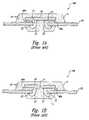
- a microelectronic device package 10 aincludes a support member 20 having an aperture 21 .
- a microelectronic substrate 30is attached to the support member 20 with strips of adhesive tape 40 a .
- Substrate bond pads 31are then electrically connected to corresponding support member bond pads 22 with wire bonds 32 that extend through the aperture 21 .
- An encapsulant 11which includes a suspension of filler material particles 12 , is disposed over the microelectronic substrate 30 and the wire bonds 32 .
- the sizes of the filler material particles 12 in any given package 10 atypically range in a standard distribution about a selected mean value.
- One drawback with the foregoing arrangementis that the filler material particles 12 (and in particular, the largest filler material particles 12 ) can impinge on and damage the microelectronic substrate 30 . Because the larger particles 12 tend to settle toward the support members 20 , one approach to addressing the foregoing drawback is to increase the separation distance between the microelectronic substrate 30 and the support member 20 by increasing the thickness of the tape 40 a . Accordingly, an advantage of the tape 40 a is that it can be selected to have a thickness sufficient to provide the desired separation between the microelectronic substrate 30 and the support member 20 . However, a drawback with the tape 40 a is that it can be expensive to install. A further drawback is that the tape 40 a can be difficult to accurately position between the support member 20 and the microelectronic substrate 30 .
- FIG. 1Billustrates another existing microelectronic device package 10 b having a microelectronic substrate 30 attached to the support member 20 with screen printed strips of epoxy 40 b .
- the epoxy 40 bcan be easier than the tape 40 a ( FIG. 1A ) to dispense on the support member 20 , but can have other problems.
- the epoxy 40 bcan apply stresses to the sides of the microelectronic substrate 30 , but it may be difficult to control how much of the sides the epoxy 40 b contacts, making it difficult to control the stress applied to the microelectronic substrate 30 .
- the thickness of the epoxy 40 btypically ranges from about 8 microns to about 25 microns, while in some cases the desired separation between microelectronic substrate 30 and the support member 20 is greater than about 75 microns, for example, to avoid the particle impingement problem described above.
- the interfaces between the epoxy 40 b and the encapsulant 11can delaminate, which can reduce the integrity of the package 10 b .
- the interface located beneath the microelectronic substrate 30can also create a high stress region that can cause a crack C to form in the encapsulant 11 .
- the crack Ccan damage the integrity of the wire bond 32 .
- the coefficient of thermal expansion (CTE) of these componentsis typically substantially different than the CTE of other components of the package.
- the microelectronic substrate 30typically has a CTE of about 3 parts per million (ppm) per ° C.
- the support member 20typically has a coefficient CTE of about 50 ppm/° C.
- the encapsulant 11typically has a CTE of from about 10–15 ppm/° C.
- the tape 40 a and the epoxy 40 beach have a CTE of about 150–400 ppm/° C.
- both the tape 40 a and the epoxy 40 bcan exert substantial shear and/or normal forces on the microelectronic substrate 30 during thermal excursions for curing, reflow and other processes. These forces can crack the microelectronic substrate 30 , and/or delaminate layers from the microelectronic substrate 30 and/or the support member 20 , causing the package to fail.
- a method in accordance with one aspect of the inventionincludes providing a support member having a first surface, a second surface facing opposite the first surface, and a projection extending away from the first surface.
- the methodcan further include forming an attachment structure by applying a quantity of adhesive material to the projection and connecting the adhesive material to the microelectronic substrate with a surface of the microelectronic substrate facing toward the first surface of the support member and with the attachment structure providing no electrically conductive link between the microelectronic substrate and the support member.
- the microelectronic substrate and the support membercan then be electrically connected, for example, with a wire bond.
- the projectioncan include an electrically conductive material, such as copper or aluminum.
- the projectioncan have the same composition as the adhesive material.
- the attachment structurecan be formed by disposing a first quantity of material on at least one of the microelectronic substrate and the support member while the first quantity of material is at least partially flowable. The flowability of the first quantity of material can be at least partially reduced, and a second quantity of material can be applied to the attachment structure while the second quantity of material is at least partially flowable. The attachment structure can then be connected to the other of the microelectronic substrate and the support member.
- the attachment structurecan have a first bond strength at a joint with the support member, and a second bond strength at a joint with the microelectronic substrate, with the second bond strength greater than the first bond strength.
- the height of the attachment structurecan be about 35 microns or more in one embodiment, and can exceed 75 microns in another embodiment.
- the attachment structurecan be connected between two microelectronic substrates.
- FIG. 1Ais a cross-sectional view of a microelectronic device package having a tape adhesive in accordance with the prior art.
- FIG. 1Bis a cross-sectional view of a microelectronic device package having an epoxy adhesive in accordance with the prior art.
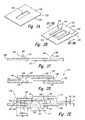
- FIGS. 2A–2Eillustrate a process for attaching a microelectronic substrate to a support member in accordance with an embodiment of the invention.
- FIGS. 3A–3Eillustrate an in-line process for attaching a microelectronic substrate to a support member in accordance with another embodiment of the invention.
- FIG. 4is a partially schematic isometric view of a support member having attachment structures in accordance with another embodiment of the invention.
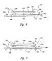
- FIG. 5is a cross-sectional view of a microelectronic package having attachment structures in accordance with still another embodiment of the invention.
- FIG. 6is a cross-sectional view of a microelectronic substrate mounted to a support member to form a package in accordance with another embodiment of the invention.
- FIG. 7is a cross-sectional view of two microelectronic substrates attached to each other with attachment structures in accordance with another embodiment of the invention.
- microelectronic substrate packagesand methods for forming such packages.
- microelectronic substrateis used throughout to include substrates upon which and/or in which microelectronic circuits or components, data storage elements or layers, and/or vias or conductive lines are or can be fabricated.
- FIGS. 2A–7Many specific details of certain embodiments of the invention are set forth in the following description and in FIGS. 2A–7 to provide a thorough understanding of these embodiments.
- FIGS. 2A–7to provide a thorough understanding of these embodiments.
- the present inventionmay have additional embodiments, and that the invention may be practiced without several of the details described below.
- FIGS. 2A–2Eillustrate a process for attaching a microelectronic substrate to a support member to form a microelectronic package in accordance with an embodiment of the invention.
- the processcan include providing a support member 120 (such as a printed circuit board) having a generally flat, planar shape with a first surface 123 and a second surface 124 facing opposite from the first surface 123 .
- An aperture 121can extend through the support member 120 from the first surface 123 to the second surface 124 to receive conductive couplers, as described in greater detail below with reference to FIG. 2E .
- Each attachment structure 140can include a projection 141 that extends away from the first surface 123 .
- the projections 141can be formed from any of a variety of materials in accordance with any of a variety of methods.
- the projections 141can include a conductive material, such as copper or aluminum, disposed on the support member 120 in a process such as a chemical vapor deposition, physical vapor deposition, or electrochemical deposition process.
- the projections 141can then be shaped using conventional etching techniques.
- the projections 141can include nonconductive materials, such as a solder mask material, an epoxy material, or an adhesive strip (e.g., a tape material).
- the projections 141can include a flowable die attach material, as described in greater detail below with reference to FIGS. 3A–3E .
- the projections 141can be formed integrally with the support member 120 , for example during the initial manufacture of the support member 120 . In any of these embodiments, the projections 141 can be positioned to support a microelectronic substrate relative to the support member 120 .
- FIG. 2Cis a cross-sectional view of the support member 120 shown in FIG. 2B , with adhesive material portions 142 disposed on each of the projections 141 .
- the adhesive materials portions 142can include a conventional die attach material, such as QMI 536, available from Dexter Electronic Materials, a business of Loktite Corporation of Rocky Hills, Conn., or 2025D, available from Ablestik of Rancho Dominguez, Calif.
- the adhesive material portions 142can include other materials.
- the adhesive material portions 142can include adhesive tape strips, such as double-backed tape strips.
- the adhesive material portions 142can be selected to adhere to both the projection 141 and a microelectronic substrate, as described in greater detail below with reference to FIG. 2D .
- a microelectronic substrate 130can be connected to and/or carried by the attachment structures 140 by contacting the microelectronic substrate 130 with the adhesive material portions 142 to form a microelectronic package 110 .
- the attachment structures 140can include a first joint 143 at the interface with the support member 120 , and a second joint 144 at the interface with the microelectronic substrate 130 .
- the first joint 143 and the second joint 144can be selected to have different strengths.
- the support member 120 , the microelectronic substrate 130 , and/or or the attachment structure 140have unequal coefficients of thermal expansion (CTEs), and this mismatch is large enough to cause the connection between the support member 120 and the microelectronic substrate 130 to fail, it may be desirable to have the failure occur at the first joint 143 (where the attachment structure 140 joins the support member 120 ) rather than at the second joint 144 (where the attachment structure 140 joins the microelectronic substrate 130 ).
- the attachment structure 140can cause damage to the component from which it separates, it may be desirable to confine such damage to the support member 120 rather than allow the microelectronic substrate 130 to be damaged.
- the projections 141can include the QMI 536 material referred to above, and the adhesive material portions 142 can include 2025D die attach adhesive. In other embodiments, other materials can be selected for the projections 141 and the adhesive material portions 142 . In any of these embodiments, the adhesive material portions 142 can include a material that is at least initially flowable and is disposed in its flowable state on the projection 141 .
- portions of the attachment structures 140can include electrically conductive materials, but the attachment structures 140 do not provide a conductive link between the support member 120 and the microelectronic substrate 130 .
- the projections 141can include an electrically conductive material while the adhesive material 142 includes an insulative material.
- other portions of the attachment structures 140can be insulative so that the attachment structures 140 do not provide a conductive link between the support member 120 and the microelectronic substrate 130 . Instead, electrical communication between these components can be provided by separate conductive couplers, as described below with reference to FIG. 2E .
- the microelectronic substrate 130can be electrically connected to the support member 120 with conductive couplers 132 , such as wire bonds.
- the conductive couplers 132can extend between substrate bond pads 131 positioned on the lower surface of the microelectronic substrate 130 , and support member bond pads 122 positioned on the second surface 124 of the support member 120 . Accordingly, the conductive couplers 132 can extend through the aperture 121 of the support member 120 .
- An encapsulant 111can then be disposed over the microelectronic substrate 130 and at least a portion of the support member 120 to protect the physical and electrical connections between the microelectronic substrate 130 and the support member 120 . Alternatively, the encapsulant 111 can be eliminated.
- the microelectronic substrate 130 and the associated electrical connectionscan be protected with a hollow cap disposed over the support member 120 .
- a distance D 1 between the microelectronic substrate 130 and the support member 120can be selected to enhance the performance of the package 110 .
- the distance D 1can be selected to be greater than 25 microns (the distance conventionally achievable with an epoxy bond) and, in a further aspect of this embodiment, the distance D 1 can be selected to be 35 microns or greater.
- the distance D 1can be selected to be about 75 microns, or 100 microns, or greater to reduce the likelihood for filler material disposed in the encapsulant 111 to impinge on and damage the microelectronic substrate 130 .
- a distance D 2(by which the projection 141 extends above the support member 120 ), and a distance D 3 (by which the adhesive material volume 142 extends above the projection 141 ) can be selected in a variety of manners to achieve the overall separation distance D 1 described above.
- D 2can be relatively large and D 3 relatively small to reduce the volume occupied by the adhesive material 142 .
- the relative values of D 2 and D 3can be reversed.
- the distance D 2can have a value of from about 8 microns to about 25 microns.
- the lateral extent of the attachment structures 140can be selected to enhance the performance of the package 110 .
- the attachment structures 140can be positioned only beneath the microelectronic substrate 130 , rather than extending around the sides of the microelectronic substrate 130 as typically occurs with some conventional epoxy bonds.
- An advantage of this arrangement, when compared to some conventional epoxy bondsis that attachment structures 140 can be less likely to impose damaging stresses on the microelectronic substrate 130 .
- a lateral extent W 1 of the attachment structure 140can be significantly less than a lateral extent W 2 of the region of the microelectronic substrate 130 that overlaps the support member 120 .
- W 1can have a value of from about 1 ⁇ 3 to about 1 ⁇ 2 of the value of W 2 .
- a feature of this arrangementis that the volume of the attachment structure 140 can be reduced relative to the overall volume of the encapsulant 111 .
- An advantage of this arrangementis that it can reduce or eliminate damage caused by CTE mismatch.
- the encapsulant 111may have a CTE that is more closely matched to that of the microelectronic substrate 130 and/or the support member 120
- the attachment structure 140may have a CTE quite different from that of the microelectronic substrate 130 and/or the support member 120 . Accordingly, by controlling the lateral extent W 1 of the attachment structures 140 , the fraction of the volume between the support member 120 and the microelectronic substrate 130 occupied by the attachment structure 140 can be reduced compared with some conventional arrangements. As a result, the attachment structure 140 can be less likely to fail or cause the microelectronic substrate 130 to fail when the package 110 undergoes thermal excursions.
- attachment structure 140can be recessed outwardly from the edge of the aperture 121 .
- An advantage of this featureis that the potential high stress at the interface between the attachment structure 140 and the encapsulant 111 can be shifted outwardly and can be less likely than existing arrangements (such as that described above with reference to FIG. 1B ) to crack the encapsulant 111 .
- FIGS. 3A–3Eschematically illustrate a process for forming a microelectronic package 110 generally similar to that described above with reference to FIGS. 2A–2E .
- the processcan be performed by in-line die attach tools, such as are available from Datacon of Radfeld/Tyrole, Austria, or ESEC of Cham, Switzerland. In other embodiments, the process can be performed by other tools.
- the processcan include providing a support member 120 having an aperture 121 .
- the support member 120can be positioned beneath a dispense nozzle 350 .
- the dispense nozzle 350can dispose two quantities of a first material 345 onto the support member 120 , while the first material 345 is in a flowable state, to form two projections 341 extending away from the first surface 123 of the support member 120 .
- the projections 341can define, at least in part, corresponding attachment structures 340 .
- the dispense nozzle 350can dispense a conventional die-attach material, such as QMI 536 or 2025D, described above.
- the dispense nozzle 350can dispose other initially flowable materials.
- the amount of the first material 345 dispensed on the support member 120 and the distance D 2 by which the resulting projections 341 extend beyond the first surface 123can be low enough that the projections 341 maintain their shape without collapsing or slumping.
- the projections 341can have a height of from about 8 microns to about 25 microns in one embodiment.
- the flowability of the first material 345can be reduced or eliminated after it has been dispensed on the support member 120 , for example, by applying heat to the first material 345 .
- the first material 345can be a thermoset material and can be partially cured (e.g., to B-stage) or fully cured.
- the first material 345can be “snap cured”, for example by exposure to elevated temperatures from about 150° C. to about 200° C. for a period of three seconds or less.
- the first material 345can be exposed to other temperatures and/or can be exposed for other time periods, for example, time periods of up to about ten seconds.
- the flowability of the first material 345can be reduced by other methods, for example, by cooling. In any of these embodiments, by at least reducing the flowability of the first material 345 , the material 345 will tend to retain its shape and height and can more stably and securely support a second material, as described in greater detail below with reference to FIG. 3D .
- a second material 346can be disposed on each of the projections 341 while the second material 346 is in a flowable state to increase the height of the corresponding attachment structures 340 .
- the second material 346can have a composition identical to that of the first material 345 .
- the second material 346can have a different composition than that of the first material 345 .
- the second material 346can be dispensed on the projections 341 by the same dispense nozzle 350 that dispensed the first material 345 , or by a different dispense nozzle.
- the second material 346can have adhesive properties, so as to adhere to the first material 345 and to the microelectronic substrate 130 , as described below with reference to FIG. 3E .
- the microelectronic substrate 130can be attached to the second material 346 of the attachment structures 340 .
- the resulting package 110can then be encapsulated after the microelectronic substrate 130 is electrically coupled to the support member 120 .
- the foregoing processcan include sequentially disposing first and second flowable materials to build up attachment structures having heights, widths, and bond strengths generally similar to those described above with reference to FIGS. 2A–2E .
- the in-line arrangement of this processcan result in an efficient and effective package formation procedure.
- the attachment structures and packages described above with reference to FIGS. 2A–3Ecan have other arrangements.
- the support member 120can include a plurality of attachment structures 440 that are arranged in discrete columns rather than continuous strips.
- Each attachment structure 440can include a projection 441 formed, for example, from the first material 345 .
- the projections 441can include non-flowable materials.
- Each attachment structure 440can further include a second material 346 disposed on the projection 441 .
- the second material 346can be applied in a manner generally similar to any of those described above with reference to FIGS. 2A–3E .
- the attachment structures 440can have a generally circular cross-sectional shape and in other embodiments, the attachment structure 440 can have other shapes. In one embodiment, the attachment structures 440 can be arranged in rows, and in other embodiments the attachment structures 440 can be arranged in other patterns or arrays. In any of these embodiments, the attachment structures 440 can be connected to a corresponding microelectronic substrate 130 (not shown in FIG. 4 ) in a manner generally similar to that described above.
- FIG. 5is a cross-sectional view of a package 510 having the microelectronic substrate 130 connected to the support member 120 with attachment structures 540 in accordance with another embodiment of the invention.
- each attachment structure 540can include the first material 345 , the second material 346 and a third material 547 .
- the flowability of the first material 345can be reduced before applying the second material 346
- the flowability of the second material 346can be reduced before applying the third material 547 .
- the first material 345can be replaced with a conductive or a nonconductive material disposed by processes generally similar to those described above with reference to FIG. 2B .
- the attachment structures 540can include more than three sequentially disposed quantities of material to achieve the desired separation distance D 1 and/or other characteristics.
- FIG. 6illustrates a package 610 having a microelectronic substrate 630 supported on a support member 620 in accordance with another embodiment of the invention.
- the microelectronic substrate 630can be attached to the support member 620 with attachment structures 640 having characteristics generally similar to any of those described above with reference to FIGS. 2A–5 .
- the package 610can have a “chip on board” configuration.
- the support member 620can have a first surface 623 and a second surface 624 facing opposite from the first surface 623 .
- the microelectronic substrate 630can have a first surface 634 and a second surface 635 facing opposite the first surface 634 and facing toward the first surface 623 of the support member 620 .
- the first surface 634 of the microelectronic substrate 630can include substrate bond pads 631 which are connected with conductive couplers 632 (such as wire bonds) to corresponding support member bond pads 622 positioned on the first surface 623 of the support member 620 .
- the physical and electrical connections between the microelectronic substrate 630 and the support member 620can be protected, for example, with an encapsulant, a shell, or a cap.
- FIG. 7illustrates a microelectronic package 710 having a plurality of microelectronic substrates connected to each other in accordance with another embodiment of the invention.
- the package 710can include a first microelectronic substrate 730 a having first bond pads 731 a .
- a second microelectronic substrate 730 bcan be attached to the first microelectronic substrate 730 a with attachment structures 740 having configurations generally similar to any of those described above with reference to FIGS. 2A–5 .
- the second microelectronic substrate 730 bcan include second bond pads 731 b connected to the first bond pads 731 a of the first microelectronic substrate 730 a with conductive couplers 732 , such as wire bonds. Solder balls 733 or other conductive devices can provide for electrical communication to and from the package 710 .
Landscapes
- Engineering & Computer Science (AREA)
- Microelectronics & Electronic Packaging (AREA)
- Computer Hardware Design (AREA)
- Power Engineering (AREA)
- Physics & Mathematics (AREA)
- Condensed Matter Physics & Semiconductors (AREA)
- General Physics & Mathematics (AREA)
- Die Bonding (AREA)
- Wire Bonding (AREA)
- Structures Or Materials For Encapsulating Or Coating Semiconductor Devices Or Solid State Devices (AREA)
Abstract
Description
Claims (52)
Priority Applications (2)
| Application Number | Priority Date | Filing Date | Title |
|---|---|---|---|
| US10/926,434US7091064B2 (en) | 2002-04-04 | 2004-08-24 | Method and apparatus for attaching microelectronic substrates and support members |
| US11/480,771US20070020811A1 (en) | 2002-04-04 | 2006-06-30 | Method and apparatus for attaching microelectronic substrates and support members |
Applications Claiming Priority (2)
| Application Number | Priority Date | Filing Date | Title |
|---|---|---|---|
| US10/116,645US7109588B2 (en) | 2002-04-04 | 2002-04-04 | Method and apparatus for attaching microelectronic substrates and support members |
| US10/926,434US7091064B2 (en) | 2002-04-04 | 2004-08-24 | Method and apparatus for attaching microelectronic substrates and support members |
Related Parent Applications (1)
| Application Number | Title | Priority Date | Filing Date |
|---|---|---|---|
| US10/116,645DivisionUS7109588B2 (en) | 2002-04-04 | 2002-04-04 | Method and apparatus for attaching microelectronic substrates and support members |
Related Child Applications (1)
| Application Number | Title | Priority Date | Filing Date |
|---|---|---|---|
| US11/480,771ContinuationUS20070020811A1 (en) | 2002-04-04 | 2006-06-30 | Method and apparatus for attaching microelectronic substrates and support members |
Publications (2)
| Publication Number | Publication Date |
|---|---|
| US20050019988A1 US20050019988A1 (en) | 2005-01-27 |
| US7091064B2true US7091064B2 (en) | 2006-08-15 |
Family
ID=28674041
Family Applications (4)
| Application Number | Title | Priority Date | Filing Date |
|---|---|---|---|
| US10/116,645Expired - Fee RelatedUS7109588B2 (en) | 2002-04-04 | 2002-04-04 | Method and apparatus for attaching microelectronic substrates and support members |
| US10/926,434Expired - Fee RelatedUS7091064B2 (en) | 2002-04-04 | 2004-08-24 | Method and apparatus for attaching microelectronic substrates and support members |
| US11/480,755Expired - LifetimeUS7615871B2 (en) | 2002-04-04 | 2006-06-30 | Method and apparatus for attaching microelectronic substrates and support members |
| US11/480,771AbandonedUS20070020811A1 (en) | 2002-04-04 | 2006-06-30 | Method and apparatus for attaching microelectronic substrates and support members |
Family Applications Before (1)
| Application Number | Title | Priority Date | Filing Date |
|---|---|---|---|
| US10/116,645Expired - Fee RelatedUS7109588B2 (en) | 2002-04-04 | 2002-04-04 | Method and apparatus for attaching microelectronic substrates and support members |
Family Applications After (2)
| Application Number | Title | Priority Date | Filing Date |
|---|---|---|---|
| US11/480,755Expired - LifetimeUS7615871B2 (en) | 2002-04-04 | 2006-06-30 | Method and apparatus for attaching microelectronic substrates and support members |
| US11/480,771AbandonedUS20070020811A1 (en) | 2002-04-04 | 2006-06-30 | Method and apparatus for attaching microelectronic substrates and support members |
Country Status (1)
| Country | Link |
|---|---|
| US (4) | US7109588B2 (en) |
Cited By (26)
| Publication number | Priority date | Publication date | Assignee | Title |
|---|---|---|---|---|
| US20060145362A1 (en)* | 2005-01-06 | 2006-07-06 | Chin-Huang Chang | Semiconductor package and fabrication method of the same |
| US20070020811A1 (en)* | 2002-04-04 | 2007-01-25 | Micron Technology, Inc. | Method and apparatus for attaching microelectronic substrates and support members |
| US8254155B1 (en) | 2011-10-03 | 2012-08-28 | Invensas Corporation | Stub minimization for multi-die wirebond assemblies with orthogonal windows |
| US8345441B1 (en) | 2011-10-03 | 2013-01-01 | Invensas Corporation | Stub minimization for multi-die wirebond assemblies with parallel windows |
| US8405207B1 (en) | 2011-10-03 | 2013-03-26 | Invensas Corporation | Stub minimization for wirebond assemblies without windows |
| US8436477B2 (en) | 2011-10-03 | 2013-05-07 | Invensas Corporation | Stub minimization using duplicate sets of signal terminals in assemblies without wirebonds to package substrate |
| US8441111B2 (en) | 2011-10-03 | 2013-05-14 | Invensas Corporation | Stub minimization for multi-die wirebond assemblies with parallel windows |
| US8502390B2 (en) | 2011-07-12 | 2013-08-06 | Tessera, Inc. | De-skewed multi-die packages |
| US8513813B2 (en) | 2011-10-03 | 2013-08-20 | Invensas Corporation | Stub minimization using duplicate sets of terminals for wirebond assemblies without windows |
| US8513817B2 (en) | 2011-07-12 | 2013-08-20 | Invensas Corporation | Memory module in a package |
| US8525327B2 (en) | 2011-10-03 | 2013-09-03 | Invensas Corporation | Stub minimization for assemblies without wirebonds to package substrate |
| US8670261B2 (en) | 2011-10-03 | 2014-03-11 | Invensas Corporation | Stub minimization using duplicate sets of signal terminals |
| US8787034B2 (en) | 2012-08-27 | 2014-07-22 | Invensas Corporation | Co-support system and microelectronic assembly |
| US8823165B2 (en) | 2011-07-12 | 2014-09-02 | Invensas Corporation | Memory module in a package |
| US8848391B2 (en) | 2012-08-27 | 2014-09-30 | Invensas Corporation | Co-support component and microelectronic assembly |
| US8848392B2 (en) | 2012-08-27 | 2014-09-30 | Invensas Corporation | Co-support module and microelectronic assembly |
| US8917532B2 (en) | 2011-10-03 | 2014-12-23 | Invensas Corporation | Stub minimization with terminal grids offset from center of package |
| US8981547B2 (en) | 2011-10-03 | 2015-03-17 | Invensas Corporation | Stub minimization for multi-die wirebond assemblies with parallel windows |
| US9070423B2 (en) | 2013-06-11 | 2015-06-30 | Invensas Corporation | Single package dual channel memory with co-support |
| US9123555B2 (en) | 2013-10-25 | 2015-09-01 | Invensas Corporation | Co-support for XFD packaging |
| US9281296B2 (en) | 2014-07-31 | 2016-03-08 | Invensas Corporation | Die stacking techniques in BGA memory package for small footprint CPU and memory motherboard design |
| US9368477B2 (en) | 2012-08-27 | 2016-06-14 | Invensas Corporation | Co-support circuit panel and microelectronic packages |
| US9484080B1 (en) | 2015-11-09 | 2016-11-01 | Invensas Corporation | High-bandwidth memory application with controlled impedance loading |
| US9679613B1 (en) | 2016-05-06 | 2017-06-13 | Invensas Corporation | TFD I/O partition for high-speed, high-density applications |
| US9691437B2 (en) | 2014-09-25 | 2017-06-27 | Invensas Corporation | Compact microelectronic assembly having reduced spacing between controller and memory packages |
| US11164804B2 (en) | 2019-07-23 | 2021-11-02 | International Business Machines Corporation | Integrated circuit (IC) device package lid attach utilizing nano particle metallic paste |
Families Citing this family (9)
| Publication number | Priority date | Publication date | Assignee | Title |
|---|---|---|---|---|
| DE102004037610B3 (en)* | 2004-08-03 | 2006-03-16 | Infineon Technologies Ag | Integrated circuit connection method e.g. for substrate and circuit assembly, involves planning flexible intermediate layer on integrated circuit and or substrate with flexible layer structured in raised and lower ranges |
| EP1630865A1 (en)* | 2004-08-17 | 2006-03-01 | Optimum Care International Tech. Inc. | Adhesion of a Chip on a leadframe |
| US8278751B2 (en) | 2005-02-08 | 2012-10-02 | Micron Technology, Inc. | Methods of adhering microfeature workpieces, including a chip, to a support member |
| US20070080435A1 (en)* | 2005-10-06 | 2007-04-12 | Chun-Hung Lin | Semiconductor packaging process and carrier for semiconductor package |
| US8072547B2 (en)* | 2006-03-31 | 2011-12-06 | Conexant Systems, Inc. | Comb filter that utilizes host memory |
| TWI378547B (en)* | 2007-09-14 | 2012-12-01 | Chipmos Technologies Inc | Multi-chip stacked package structure |
| TWI380424B (en)* | 2009-02-27 | 2012-12-21 | Walton Advanced Eng Inc | Window type semiconductor package |
| KR101630394B1 (en)* | 2010-03-08 | 2016-06-24 | 삼성전자주식회사 | Package substrate, semiconductor package comprising the same and method for fabricating the semiconductor package |
| WO2017107030A1 (en)* | 2015-12-22 | 2017-06-29 | Intel Corporation | Eliminating die shadow effects by dummy die beams for solder joint reliability improvement |
Citations (97)
| Publication number | Priority date | Publication date | Assignee | Title |
|---|---|---|---|---|
| US5139973A (en) | 1990-12-17 | 1992-08-18 | Allegro Microsystems, Inc. | Method for making a semiconductor package with the distance between a lead frame die pad and heat spreader determined by the thickness of an intermediary insulating sheet |
| US5208188A (en) | 1989-10-02 | 1993-05-04 | Advanced Micro Devices, Inc. | Process for making a multilayer lead frame assembly for an integrated circuit structure and multilayer integrated circuit die package formed by such process |
| US5593927A (en) | 1993-10-14 | 1997-01-14 | Micron Technology, Inc. | Method for packaging semiconductor dice |
| US5677566A (en) | 1995-05-08 | 1997-10-14 | Micron Technology, Inc. | Semiconductor chip package |
| US5696033A (en) | 1995-08-16 | 1997-12-09 | Micron Technology, Inc. | Method for packaging a semiconductor die |
| US5739585A (en) | 1995-11-27 | 1998-04-14 | Micron Technology, Inc. | Single piece package for semiconductor die |
| USD394844S (en) | 1997-04-25 | 1998-06-02 | Micron Technology, Inc. | Temporary package for semiconductor dice |
| USD402638S (en) | 1997-04-25 | 1998-12-15 | Micron Technology, Inc. | Temporary package for semiconductor dice |
| US5851845A (en) | 1995-12-18 | 1998-12-22 | Micron Technology, Inc. | Process for packaging a semiconductor die using dicing and testing |
| US5866953A (en) | 1996-05-24 | 1999-02-02 | Micron Technology, Inc. | Packaged die on PCB with heat sink encapsulant |
| US5891753A (en) | 1997-01-24 | 1999-04-06 | Micron Technology, Inc. | Method and apparatus for packaging flip chip bare die on printed circuit boards |
| US5893726A (en) | 1997-12-15 | 1999-04-13 | Micron Technology, Inc. | Semiconductor package with pre-fabricated cover and method of fabrication |
| US5920118A (en) | 1996-12-18 | 1999-07-06 | Hyundai Electronics Industries Co., Ltd. | Chip-size package semiconductor |
| US5933713A (en) | 1998-04-06 | 1999-08-03 | Micron Technology, Inc. | Method of forming overmolded chip scale package and resulting product |
| US5938956A (en) | 1996-09-10 | 1999-08-17 | Micron Technology, Inc. | Circuit and method for heating an adhesive to package or rework a semiconductor die |
| US5956236A (en) | 1997-11-25 | 1999-09-21 | Micron Technology, Inc. | Integrated circuit package support system |
| US5958100A (en) | 1993-06-03 | 1999-09-28 | Micron Technology, Inc. | Process of making a glass semiconductor package |
| US5986209A (en) | 1997-07-09 | 1999-11-16 | Micron Technology, Inc. | Package stack via bottom leaded plastic (BLP) packaging |
| US5989941A (en) | 1997-12-12 | 1999-11-23 | Micron Technology, Inc. | Encapsulated integrated circuit packaging |
| US5990566A (en) | 1998-05-20 | 1999-11-23 | Micron Technology, Inc. | High density semiconductor package |
| US5994784A (en) | 1997-12-18 | 1999-11-30 | Micron Technology, Inc. | Die positioning in integrated circuit packaging |
| USRE36469E (en) | 1988-09-30 | 1999-12-28 | Micron Technology, Inc. | Packaging for semiconductor logic devices |
| US6008074A (en) | 1998-10-01 | 1999-12-28 | Micron Technology, Inc. | Method of forming a synchronous-link dynamic random access memory edge-mounted device |
| US6008070A (en) | 1998-05-21 | 1999-12-28 | Micron Technology, Inc. | Wafer level fabrication and assembly of chip scale packages |
| US6017776A (en) | 1997-04-29 | 2000-01-25 | Micron Technology, Inc. | Method of attaching a leadframe to singulated semiconductor dice |
| US6020629A (en) | 1998-06-05 | 2000-02-01 | Micron Technology, Inc. | Stacked semiconductor package and method of fabrication |
| US6025728A (en) | 1997-04-25 | 2000-02-15 | Micron Technology, Inc. | Semiconductor package with wire bond protective member |
| US6028365A (en) | 1998-03-30 | 2000-02-22 | Micron Technology, Inc. | Integrated circuit package and method of fabrication |
| US6046496A (en) | 1997-11-04 | 2000-04-04 | Micron Technology Inc | Chip package |
| US6049125A (en) | 1997-12-29 | 2000-04-11 | Micron Technology, Inc. | Semiconductor package with heat sink and method of fabrication |
| US6048755A (en) | 1998-11-12 | 2000-04-11 | Micron Technology, Inc. | Method for fabricating BGA package using substrate with patterned solder mask open in die attach area |
| US6048744A (en) | 1997-09-15 | 2000-04-11 | Micron Technology, Inc. | Integrated circuit package alignment feature |
| US6072236A (en) | 1996-03-07 | 2000-06-06 | Micron Technology, Inc. | Micromachined chip scale package |
| US6075288A (en) | 1998-06-08 | 2000-06-13 | Micron Technology, Inc. | Semiconductor package having interlocking heat sinks and method of fabrication |
| US6089920A (en) | 1998-05-04 | 2000-07-18 | Micron Technology, Inc. | Modular die sockets with flexible interconnects for packaging bare semiconductor die |
| US6097087A (en) | 1997-10-31 | 2000-08-01 | Micron Technology, Inc. | Semiconductor package including flex circuit, interconnects and dense array external contacts |
| US6103547A (en) | 1997-01-17 | 2000-08-15 | Micron Technology, Inc. | High speed IC package configuration |
| US6107680A (en) | 1995-01-04 | 2000-08-22 | Micron Technology, Inc. | Packaging for bare dice employing EMR-sensitive adhesives |
| US6107122A (en) | 1997-08-04 | 2000-08-22 | Micron Technology, Inc. | Direct die contact (DDC) semiconductor package |
| US6117382A (en) | 1998-02-05 | 2000-09-12 | Micron Technology, Inc. | Method for encasing array packages |
| US6159764A (en) | 1997-07-02 | 2000-12-12 | Micron Technology, Inc. | Varied-thickness heat sink for integrated circuit (IC) packages and method of fabricating IC packages |
| US6172419B1 (en) | 1998-02-24 | 2001-01-09 | Micron Technology, Inc. | Low profile ball grid array package |
| US6175159B1 (en) | 1997-07-16 | 2001-01-16 | Oki Electric Industry Co., Ltd. | Semiconductor package |
| US6184465B1 (en) | 1998-11-12 | 2001-02-06 | Micron Technology, Inc. | Semiconductor package |
| US6198172B1 (en) | 1997-02-20 | 2001-03-06 | Micron Technology, Inc. | Semiconductor chip package |
| US6208519B1 (en) | 1999-08-31 | 2001-03-27 | Micron Technology, Inc. | Thermally enhanced semiconductor package |
| US6210992B1 (en) | 1999-08-31 | 2001-04-03 | Micron Technology, Inc. | Controlling packaging encapsulant leakage |
| US6215175B1 (en) | 1998-07-06 | 2001-04-10 | Micron Technology, Inc. | Semiconductor package having metal foil die mounting plate |
| US6218731B1 (en)* | 1999-05-21 | 2001-04-17 | Siliconware Precision Industries Co., Ltd. | Tiny ball grid array package |
| US6228548B1 (en) | 1998-02-27 | 2001-05-08 | Micron Technology, Inc. | Method of making a multichip semiconductor package |
| US6229202B1 (en) | 2000-01-10 | 2001-05-08 | Micron Technology, Inc. | Semiconductor package having downset leadframe for reducing package bow |
| US6259153B1 (en) | 1998-08-20 | 2001-07-10 | Micron Technology, Inc. | Transverse hybrid LOC package |
| US6277671B1 (en) | 1998-10-20 | 2001-08-21 | Micron Technology, Inc. | Methods of forming integrated circuit packages |
| US6284571B1 (en) | 1997-07-02 | 2001-09-04 | Micron Technology, Inc. | Lead frame assemblies with voltage reference plane and IC packages including same |
| US6291894B1 (en) | 1998-08-31 | 2001-09-18 | Micron Technology, Inc. | Method and apparatus for a semiconductor package for vertical surface mounting |
| US6294839B1 (en) | 1999-08-30 | 2001-09-25 | Micron Technology, Inc. | Apparatus and methods of packaging and testing die |
| US6303985B1 (en) | 1998-11-12 | 2001-10-16 | Micron Technology, Inc. | Semiconductor lead frame and package with stiffened mounting paddle |
| US6303981B1 (en) | 1999-09-01 | 2001-10-16 | Micron Technology, Inc. | Semiconductor package having stacked dice and leadframes and method of fabrication |
| US6310390B1 (en) | 1999-04-08 | 2001-10-30 | Micron Technology, Inc. | BGA package and method of fabrication |
| US6310288B1 (en) | 1996-05-21 | 2001-10-30 | Micron Technology, Inc. | Underfill coating for loc package |
| US6316285B1 (en) | 1998-09-02 | 2001-11-13 | Micron Technology, Inc. | Passivation layer for packaged integrated circuits |
| US6314639B1 (en) | 1998-02-23 | 2001-11-13 | Micron Technology, Inc. | Chip scale package with heat spreader and method of manufacture |
| US6326698B1 (en) | 2000-06-08 | 2001-12-04 | Micron Technology, Inc. | Semiconductor devices having protective layers thereon through which contact pads are exposed and stereolithographic methods of fabricating such semiconductor devices |
| US6326687B1 (en) | 1998-09-01 | 2001-12-04 | Micron Technology, Inc. | IC package with dual heat spreaders |
| US6326244B1 (en) | 1998-09-03 | 2001-12-04 | Micron Technology, Inc. | Method of making a cavity ball grid array apparatus |
| US6329220B1 (en) | 1999-11-23 | 2001-12-11 | Micron Technology, Inc. | Packages for semiconductor die |
| US6331221B1 (en) | 1998-04-15 | 2001-12-18 | Micron Technology, Inc. | Process for providing electrical connection between a semiconductor die and a semiconductor die receiving member |
| US6331453B1 (en) | 1999-12-16 | 2001-12-18 | Micron Technology, Inc. | Method for fabricating semiconductor packages using mold tooling fixture with flash control cavities |
| US6333564B1 (en) | 1998-06-22 | 2001-12-25 | Fujitsu Limited | Surface mount type semiconductor device and method of producing the same having an interposing layer electrically connecting the semiconductor chip with protrusion electrodes |
| US6342728B2 (en) | 1996-03-22 | 2002-01-29 | Hitachi, Ltd. | Semiconductor device and manufacturing method thereof |
| US6365434B1 (en) | 2000-06-28 | 2002-04-02 | Micron Technology, Inc. | Method and apparatus for reduced flash encapsulation of microelectronic devices |
| US6385049B1 (en) | 2001-07-05 | 2002-05-07 | Walsin Advanced Electronics Ltd | Multi-board BGA package |
| US6396129B1 (en) | 2001-03-05 | 2002-05-28 | Siliconware Precision Industries Co., Ltd. | Leadframe with dot array of silver-plated regions on die pad for use in exposed-pad semiconductor package |
| US6451709B1 (en) | 1998-09-03 | 2002-09-17 | Micron Technology, Inc. | Methodology of removing misplaced encapsulant for attachment of heat sinks in a chip on board package |
| US6455354B1 (en) | 1998-12-30 | 2002-09-24 | Micron Technology, Inc. | Method of fabricating tape attachment chip-on-board assemblies |
| US6479323B1 (en) | 1995-09-19 | 2002-11-12 | National Semiconductor Corporation | Method for attaching a lead frame to a heat spreader/heat slug structure |
| US6501170B1 (en) | 2000-06-09 | 2002-12-31 | Micron Technology, Inc. | Substrates and assemblies including pre-applied adhesion promoter |
| US6528408B2 (en) | 2001-05-21 | 2003-03-04 | Micron Technology, Inc. | Method for bumped die and wire bonded board-on-chip package |
| US6528722B2 (en) | 1998-07-31 | 2003-03-04 | Siliconware Precision Industries Co., Ltd. | Ball grid array semiconductor package with exposed base layer |
| US6548757B1 (en) | 2000-08-28 | 2003-04-15 | Micron Technology, Inc. | Microelectronic device assemblies having a shielded input and methods for manufacturing and operating such microelectronic device assemblies |
| US6558600B1 (en) | 2000-05-04 | 2003-05-06 | Micron Technology, Inc. | Method for packaging microelectronic substrates |
| US6561479B1 (en) | 2000-08-23 | 2003-05-13 | Micron Technology, Inc. | Small scale actuators and methods for their formation and use |
| US6564979B2 (en) | 2001-07-18 | 2003-05-20 | Micron Technology, Inc. | Method and apparatus for dispensing adhesive on microelectronic substrate supports |
| US6576494B1 (en) | 2000-06-28 | 2003-06-10 | Micron Technology, Inc. | Recessed encapsulated microelectronic devices and methods for formation |
| US6576495B1 (en) | 2000-08-30 | 2003-06-10 | Micron Technology, Inc. | Microelectronic assembly with pre-disposed fill material and associated method of manufacture |
| US6589820B1 (en) | 2000-06-16 | 2003-07-08 | Micron Technology, Inc. | Method and apparatus for packaging a microelectronic die |
| US6614092B2 (en) | 2000-08-16 | 2003-09-02 | Micron Technology, Inc. | Microelectronic device package with conductive elements and associated method of manufacture |
| US6622380B1 (en) | 2002-02-12 | 2003-09-23 | Micron Technology, Inc. | Methods for manufacturing microelectronic devices and methods for mounting microelectronic packages to circuit boards |
| US6656769B2 (en) | 2000-05-08 | 2003-12-02 | Micron Technology, Inc. | Method and apparatus for distributing mold material in a mold for packaging microelectronic devices |
| US6670719B2 (en) | 1999-08-25 | 2003-12-30 | Micron Technology, Inc. | Microelectronic device package filled with liquid or pressurized gas and associated method of manufacture |
| US6673649B1 (en) | 2002-07-05 | 2004-01-06 | Micron Technology, Inc. | Microelectronic device packages and methods for controlling the disposition of non-conductive materials in such packages |
| US6724076B1 (en) | 1999-11-15 | 2004-04-20 | Infineon Technologies Ag | Package for a semiconductor chip |
| US20040159942A1 (en) | 2002-08-02 | 2004-08-19 | Kinsman Larry D. | Semiconductor package and method producing same |
| US20040265549A1 (en) | 1998-12-12 | 2004-12-30 | Kydd Paul H | Adhesiveless transfer lamination method and materials for producing electronic circuits |
| US20050006743A1 (en) | 2003-07-01 | 2005-01-13 | Kim Tae-Hyun | In-line apparatus and method for manufacturing double-sided stacked multi-chip packages |
| US20050019988A1 (en) | 2002-04-04 | 2005-01-27 | Tongbi Jiang | Method and apparatus for attaching microelectronic substrates and support members |
| US20050230821A1 (en) | 2004-04-15 | 2005-10-20 | Kheng Lee T | Semiconductor packages, and methods of forming semiconductor packages |
Family Cites Families (59)
| Publication number | Priority date | Publication date | Assignee | Title |
|---|---|---|---|---|
| US4563811A (en)* | 1983-10-28 | 1986-01-14 | At&T Technologies, Inc. | Method of making a dual-in-line package |
| US5946553A (en) | 1991-06-04 | 1999-08-31 | Micron Technology, Inc. | Process for manufacturing a semiconductor package with bi-substrate die |
| US5252857A (en) | 1991-08-05 | 1993-10-12 | International Business Machines Corporation | Stacked DCA memory chips |
| US5614766A (en)* | 1991-09-30 | 1997-03-25 | Rohm Co., Ltd. | Semiconductor device with stacked alternate-facing chips |
| KR940008327B1 (en) | 1991-10-10 | 1994-09-12 | 삼성전자 주식회사 | Semiconductor package and its mounting method |
| US5128831A (en) | 1991-10-31 | 1992-07-07 | Micron Technology, Inc. | High-density electronic package comprising stacked sub-modules which are electrically interconnected by solder-filled vias |
| US5422435A (en)* | 1992-05-22 | 1995-06-06 | National Semiconductor Corporation | Stacked multi-chip modules and method of manufacturing |
| US5535101A (en)* | 1992-11-03 | 1996-07-09 | Motorola, Inc. | Leadless integrated circuit package |
| JP3404795B2 (en) | 1993-03-31 | 2003-05-12 | 東レ株式会社 | Epoxy resin composition for semiconductor encapsulation |
| JPH07263382A (en) | 1994-03-24 | 1995-10-13 | Kawasaki Steel Corp | Wafer fixing tape |
| JPH07307416A (en) | 1994-05-12 | 1995-11-21 | Toshiba Corp | Semiconductor chip mounting method and semiconductor device |
| US6013948A (en) | 1995-11-27 | 2000-01-11 | Micron Technology, Inc. | Stackable chip scale semiconductor package with mating contacts on opposed surfaces |
| US5855821A (en) | 1995-12-22 | 1999-01-05 | Johnson Matthey, Inc. | Materials for semiconductor device assemblies |
| JP2806357B2 (en)* | 1996-04-18 | 1998-09-30 | 日本電気株式会社 | Stack module |
| US5925930A (en)* | 1996-05-21 | 1999-07-20 | Micron Technology, Inc. | IC contacts with palladium layer and flexible conductive epoxy bumps |
| JP3195236B2 (en) | 1996-05-30 | 2001-08-06 | 株式会社日立製作所 | Wiring tape having adhesive film, semiconductor device and manufacturing method |
| DE19626126C2 (en)* | 1996-06-28 | 1998-04-16 | Fraunhofer Ges Forschung | Method for forming a spatial chip arrangement and spatial chip arrangement |
| JP2870497B2 (en) | 1996-08-01 | 1999-03-17 | 日本電気株式会社 | Semiconductor element mounting method |
| US5876498A (en) | 1996-12-20 | 1999-03-02 | Moms, Inc. | Apparatus for preserving solder paste in the manufacturing of printed circuit board assemblies |
| US5994166A (en)* | 1997-03-10 | 1999-11-30 | Micron Technology, Inc. | Method of constructing stacked packages |
| US6114769A (en) | 1997-07-18 | 2000-09-05 | Mcms, Inc. | Solder paste brick |
| US6063647A (en) | 1997-12-08 | 2000-05-16 | 3M Innovative Properties Company | Method for making circuit elements for a z-axis interconnect |
| JP3097644B2 (en) | 1998-01-06 | 2000-10-10 | 日本電気株式会社 | Semiconductor device connection structure and connection method |
| US6175149B1 (en) | 1998-02-13 | 2001-01-16 | Micron Technology, Inc. | Mounting multiple semiconductor dies in a package |
| US6297547B1 (en) | 1998-02-13 | 2001-10-02 | Micron Technology Inc. | Mounting multiple semiconductor dies in a package |
| US6002165A (en) | 1998-02-23 | 1999-12-14 | Micron Technology, Inc. | Multilayered lead frame for semiconductor packages |
| US6072233A (en) | 1998-05-04 | 2000-06-06 | Micron Technology, Inc. | Stackable ball grid array package |
| US6153929A (en)* | 1998-08-21 | 2000-11-28 | Micron Technology, Inc. | Low profile multi-IC package connector |
| US6194250B1 (en)* | 1998-09-14 | 2001-02-27 | Motorola, Inc. | Low-profile microelectronic package |
| US6261865B1 (en)* | 1998-10-06 | 2001-07-17 | Micron Technology, Inc. | Multi chip semiconductor package and method of construction |
| US6541872B1 (en) | 1999-01-11 | 2003-04-01 | Micron Technology, Inc. | Multi-layered adhesive for attaching a semiconductor die to a substrate |
| US6118176A (en) | 1999-04-26 | 2000-09-12 | Advanced Semiconductor Engineering, Inc. | Stacked chip assembly utilizing a lead frame |
| US6448635B1 (en) | 1999-08-30 | 2002-09-10 | Amkor Technology, Inc. | Surface acoustical wave flip chip |
| US6212767B1 (en)* | 1999-08-31 | 2001-04-10 | Micron Technology, Inc. | Assembling a stacked die package |
| US6316727B1 (en)* | 1999-10-07 | 2001-11-13 | United Microelectronics Corp. | Multi-chip semiconductor package |
| US6261623B1 (en)* | 1999-10-21 | 2001-07-17 | Hickory Specialties, Inc. | Method for making a liquid smoke coloring agent solution |
| JP2001127246A (en)* | 1999-10-29 | 2001-05-11 | Fujitsu Ltd | Semiconductor device |
| US6414396B1 (en)* | 2000-01-24 | 2002-07-02 | Amkor Technology, Inc. | Package for stacked integrated circuits |
| JP3491595B2 (en) | 2000-02-25 | 2004-01-26 | ソニーケミカル株式会社 | Anisotropic conductive adhesive film |
| JP2001257307A (en)* | 2000-03-09 | 2001-09-21 | Sharp Corp | Semiconductor device |
| US6265763B1 (en)* | 2000-03-14 | 2001-07-24 | Siliconware Precision Industries Co., Ltd. | Multi-chip integrated circuit package structure for central pad chip |
| US6437446B1 (en)* | 2000-03-16 | 2002-08-20 | Oki Electric Industry Co., Ltd. | Semiconductor device having first and second chips |
| JP3701542B2 (en)* | 2000-05-10 | 2005-09-28 | シャープ株式会社 | Semiconductor device and manufacturing method thereof |
| US6400033B1 (en) | 2000-06-01 | 2002-06-04 | Amkor Technology, Inc. | Reinforcing solder connections of electronic devices |
| TW445610B (en)* | 2000-06-16 | 2001-07-11 | Siliconware Precision Industries Co Ltd | Stacked-die packaging structure |
| US6552910B1 (en)* | 2000-06-28 | 2003-04-22 | Micron Technology, Inc. | Stacked-die assemblies with a plurality of microelectronic devices and methods of manufacture |
| US6560117B2 (en)* | 2000-06-28 | 2003-05-06 | Micron Technology, Inc. | Packaged microelectronic die assemblies and methods of manufacture |
| US6607937B1 (en) | 2000-08-23 | 2003-08-19 | Micron Technology, Inc. | Stacked microelectronic dies and methods for stacking microelectronic dies |
| US6503776B2 (en)* | 2001-01-05 | 2003-01-07 | Advanced Semiconductor Engineering, Inc. | Method for fabricating stacked chip package |
| US6548376B2 (en)* | 2001-08-30 | 2003-04-15 | Micron Technology, Inc. | Methods of thinning microelectronic workpieces |
| US20030134451A1 (en) | 2002-01-14 | 2003-07-17 | Picta Technology, Inc. | Structure and process for packaging back-to-back chips |
| US6885093B2 (en)* | 2002-02-28 | 2005-04-26 | Freescale Semiconductor, Inc. | Stacked die semiconductor device |
| US6753613B2 (en)* | 2002-03-13 | 2004-06-22 | Intel Corporation | Stacked dice standoffs |
| US6844618B2 (en)* | 2002-04-04 | 2005-01-18 | Micron Technology, Inc. | Microelectronic package with reduced underfill and methods for forming such packages |
| KR100429885B1 (en)* | 2002-05-09 | 2004-05-03 | 삼성전자주식회사 | Multi-chip package improving heat spread characteristics and manufacturing method the same |
| US6841858B2 (en)* | 2002-09-27 | 2005-01-11 | St Assembly Test Services Pte Ltd. | Leadframe for die stacking applications and related die stacking concepts |
| US20040067606A1 (en)* | 2002-10-02 | 2004-04-08 | Fehr Gerald K. | Method for stack-packaging integrated circuit die using at least one die in the package as a spacer |
| KR100477020B1 (en)* | 2002-12-16 | 2005-03-21 | 삼성전자주식회사 | Multi chip package |
| US8278751B2 (en) | 2005-02-08 | 2012-10-02 | Micron Technology, Inc. | Methods of adhering microfeature workpieces, including a chip, to a support member |
- 2002
- 2002-04-04USUS10/116,645patent/US7109588B2/ennot_activeExpired - Fee Related
- 2004
- 2004-08-24USUS10/926,434patent/US7091064B2/ennot_activeExpired - Fee Related
- 2006
- 2006-06-30USUS11/480,755patent/US7615871B2/ennot_activeExpired - Lifetime
- 2006-06-30USUS11/480,771patent/US20070020811A1/ennot_activeAbandoned
Patent Citations (113)
| Publication number | Priority date | Publication date | Assignee | Title |
|---|---|---|---|---|
| USRE36469E (en) | 1988-09-30 | 1999-12-28 | Micron Technology, Inc. | Packaging for semiconductor logic devices |
| US5208188A (en) | 1989-10-02 | 1993-05-04 | Advanced Micro Devices, Inc. | Process for making a multilayer lead frame assembly for an integrated circuit structure and multilayer integrated circuit die package formed by such process |
| US5139973A (en) | 1990-12-17 | 1992-08-18 | Allegro Microsystems, Inc. | Method for making a semiconductor package with the distance between a lead frame die pad and heat spreader determined by the thickness of an intermediary insulating sheet |
| US5958100A (en) | 1993-06-03 | 1999-09-28 | Micron Technology, Inc. | Process of making a glass semiconductor package |
| US5593927A (en) | 1993-10-14 | 1997-01-14 | Micron Technology, Inc. | Method for packaging semiconductor dice |
| US6107680A (en) | 1995-01-04 | 2000-08-22 | Micron Technology, Inc. | Packaging for bare dice employing EMR-sensitive adhesives |
| US5677566A (en) | 1995-05-08 | 1997-10-14 | Micron Technology, Inc. | Semiconductor chip package |
| US5696033A (en) | 1995-08-16 | 1997-12-09 | Micron Technology, Inc. | Method for packaging a semiconductor die |
| US6479323B1 (en) | 1995-09-19 | 2002-11-12 | National Semiconductor Corporation | Method for attaching a lead frame to a heat spreader/heat slug structure |
| US5739585A (en) | 1995-11-27 | 1998-04-14 | Micron Technology, Inc. | Single piece package for semiconductor die |
| US5851845A (en) | 1995-12-18 | 1998-12-22 | Micron Technology, Inc. | Process for packaging a semiconductor die using dicing and testing |
| US6124634A (en) | 1996-03-07 | 2000-09-26 | Micron Technology, Inc. | Micromachined chip scale package |
| US6072236A (en) | 1996-03-07 | 2000-06-06 | Micron Technology, Inc. | Micromachined chip scale package |
| US6342728B2 (en) | 1996-03-22 | 2002-01-29 | Hitachi, Ltd. | Semiconductor device and manufacturing method thereof |
| US6310288B1 (en) | 1996-05-21 | 2001-10-30 | Micron Technology, Inc. | Underfill coating for loc package |
| US5866953A (en) | 1996-05-24 | 1999-02-02 | Micron Technology, Inc. | Packaged die on PCB with heat sink encapsulant |
| US6252308B1 (en) | 1996-05-24 | 2001-06-26 | Micron Technology, Inc. | Packaged die PCB with heat sink encapsulant |
| US5938956A (en) | 1996-09-10 | 1999-08-17 | Micron Technology, Inc. | Circuit and method for heating an adhesive to package or rework a semiconductor die |
| US5920118A (en) | 1996-12-18 | 1999-07-06 | Hyundai Electronics Industries Co., Ltd. | Chip-size package semiconductor |
| US6103547A (en) | 1997-01-17 | 2000-08-15 | Micron Technology, Inc. | High speed IC package configuration |
| US5898224A (en) | 1997-01-24 | 1999-04-27 | Micron Technology, Inc. | Apparatus for packaging flip chip bare die on printed circuit boards |
| US5891753A (en) | 1997-01-24 | 1999-04-06 | Micron Technology, Inc. | Method and apparatus for packaging flip chip bare die on printed circuit boards |
| US6198172B1 (en) | 1997-02-20 | 2001-03-06 | Micron Technology, Inc. | Semiconductor chip package |
| US6025728A (en) | 1997-04-25 | 2000-02-15 | Micron Technology, Inc. | Semiconductor package with wire bond protective member |
| USD394844S (en) | 1997-04-25 | 1998-06-02 | Micron Technology, Inc. | Temporary package for semiconductor dice |
| USD402638S (en) | 1997-04-25 | 1998-12-15 | Micron Technology, Inc. | Temporary package for semiconductor dice |
| US6312977B1 (en) | 1997-04-29 | 2001-11-06 | Tongbi Jiang | Method of attaching a leadframe to singulated semiconductor dice |
| US6017776A (en) | 1997-04-29 | 2000-01-25 | Micron Technology, Inc. | Method of attaching a leadframe to singulated semiconductor dice |
| US6284571B1 (en) | 1997-07-02 | 2001-09-04 | Micron Technology, Inc. | Lead frame assemblies with voltage reference plane and IC packages including same |
| US6159764A (en) | 1997-07-02 | 2000-12-12 | Micron Technology, Inc. | Varied-thickness heat sink for integrated circuit (IC) packages and method of fabricating IC packages |
| US5986209A (en) | 1997-07-09 | 1999-11-16 | Micron Technology, Inc. | Package stack via bottom leaded plastic (BLP) packaging |
| US6175159B1 (en) | 1997-07-16 | 2001-01-16 | Oki Electric Industry Co., Ltd. | Semiconductor package |
| US6150717A (en) | 1997-08-04 | 2000-11-21 | Micron Technology, Inc. | Direct die contact (DDC) semiconductor package |
| US6107122A (en) | 1997-08-04 | 2000-08-22 | Micron Technology, Inc. | Direct die contact (DDC) semiconductor package |
| US6048744A (en) | 1997-09-15 | 2000-04-11 | Micron Technology, Inc. | Integrated circuit package alignment feature |
| US6246108B1 (en) | 1997-09-15 | 2001-06-12 | Micron Technology, Inc. | Integrated circuit package including lead frame with electrically isolated alignment feature |
| US6097087A (en) | 1997-10-31 | 2000-08-01 | Micron Technology, Inc. | Semiconductor package including flex circuit, interconnects and dense array external contacts |
| US6046496A (en) | 1997-11-04 | 2000-04-04 | Micron Technology Inc | Chip package |
| US5956236A (en) | 1997-11-25 | 1999-09-21 | Micron Technology, Inc. | Integrated circuit package support system |
| US5989941A (en) | 1997-12-12 | 1999-11-23 | Micron Technology, Inc. | Encapsulated integrated circuit packaging |
| US5893726A (en) | 1997-12-15 | 1999-04-13 | Micron Technology, Inc. | Semiconductor package with pre-fabricated cover and method of fabrication |
| US5994784A (en) | 1997-12-18 | 1999-11-30 | Micron Technology, Inc. | Die positioning in integrated circuit packaging |
| US6049125A (en) | 1997-12-29 | 2000-04-11 | Micron Technology, Inc. | Semiconductor package with heat sink and method of fabrication |
| US6326242B1 (en) | 1997-12-29 | 2001-12-04 | Micron Technology, Inc. | Semiconductor package with heat sink and method of fabrication |
| US6117382A (en) | 1998-02-05 | 2000-09-12 | Micron Technology, Inc. | Method for encasing array packages |
| US6332766B1 (en) | 1998-02-05 | 2001-12-25 | Micron Technology, Inc. | Apparatus for encasing array packages |
| US6314639B1 (en) | 1998-02-23 | 2001-11-13 | Micron Technology, Inc. | Chip scale package with heat spreader and method of manufacture |
| US6172419B1 (en) | 1998-02-24 | 2001-01-09 | Micron Technology, Inc. | Low profile ball grid array package |
| US6228548B1 (en) | 1998-02-27 | 2001-05-08 | Micron Technology, Inc. | Method of making a multichip semiconductor package |
| US6028365A (en) | 1998-03-30 | 2000-02-22 | Micron Technology, Inc. | Integrated circuit package and method of fabrication |
| US5933713A (en) | 1998-04-06 | 1999-08-03 | Micron Technology, Inc. | Method of forming overmolded chip scale package and resulting product |
| US6331221B1 (en) | 1998-04-15 | 2001-12-18 | Micron Technology, Inc. | Process for providing electrical connection between a semiconductor die and a semiconductor die receiving member |
| US6089920A (en) | 1998-05-04 | 2000-07-18 | Micron Technology, Inc. | Modular die sockets with flexible interconnects for packaging bare semiconductor die |
| US5990566A (en) | 1998-05-20 | 1999-11-23 | Micron Technology, Inc. | High density semiconductor package |
| US6326697B1 (en) | 1998-05-21 | 2001-12-04 | Micron Technology, Inc. | Hermetically sealed chip scale packages formed by wafer level fabrication and assembly |
| US6008070A (en) | 1998-05-21 | 1999-12-28 | Micron Technology, Inc. | Wafer level fabrication and assembly of chip scale packages |
| US6020629A (en) | 1998-06-05 | 2000-02-01 | Micron Technology, Inc. | Stacked semiconductor package and method of fabrication |
| US6075288A (en) | 1998-06-08 | 2000-06-13 | Micron Technology, Inc. | Semiconductor package having interlocking heat sinks and method of fabrication |
| US6333564B1 (en) | 1998-06-22 | 2001-12-25 | Fujitsu Limited | Surface mount type semiconductor device and method of producing the same having an interposing layer electrically connecting the semiconductor chip with protrusion electrodes |
| US6215175B1 (en) | 1998-07-06 | 2001-04-10 | Micron Technology, Inc. | Semiconductor package having metal foil die mounting plate |
| US6528722B2 (en) | 1998-07-31 | 2003-03-04 | Siliconware Precision Industries Co., Ltd. | Ball grid array semiconductor package with exposed base layer |
| US6259153B1 (en) | 1998-08-20 | 2001-07-10 | Micron Technology, Inc. | Transverse hybrid LOC package |
| US6291894B1 (en) | 1998-08-31 | 2001-09-18 | Micron Technology, Inc. | Method and apparatus for a semiconductor package for vertical surface mounting |
| US6326687B1 (en) | 1998-09-01 | 2001-12-04 | Micron Technology, Inc. | IC package with dual heat spreaders |
| US6316285B1 (en) | 1998-09-02 | 2001-11-13 | Micron Technology, Inc. | Passivation layer for packaged integrated circuits |
| US6451709B1 (en) | 1998-09-03 | 2002-09-17 | Micron Technology, Inc. | Methodology of removing misplaced encapsulant for attachment of heat sinks in a chip on board package |
| US6326244B1 (en) | 1998-09-03 | 2001-12-04 | Micron Technology, Inc. | Method of making a cavity ball grid array apparatus |
| US6008074A (en) | 1998-10-01 | 1999-12-28 | Micron Technology, Inc. | Method of forming a synchronous-link dynamic random access memory edge-mounted device |
| US6277671B1 (en) | 1998-10-20 | 2001-08-21 | Micron Technology, Inc. | Methods of forming integrated circuit packages |
| US6184465B1 (en) | 1998-11-12 | 2001-02-06 | Micron Technology, Inc. | Semiconductor package |
| US6303985B1 (en) | 1998-11-12 | 2001-10-16 | Micron Technology, Inc. | Semiconductor lead frame and package with stiffened mounting paddle |
| US6048755A (en) | 1998-11-12 | 2000-04-11 | Micron Technology, Inc. | Method for fabricating BGA package using substrate with patterned solder mask open in die attach area |
| US20040265549A1 (en) | 1998-12-12 | 2004-12-30 | Kydd Paul H | Adhesiveless transfer lamination method and materials for producing electronic circuits |
| US6455354B1 (en) | 1998-12-30 | 2002-09-24 | Micron Technology, Inc. | Method of fabricating tape attachment chip-on-board assemblies |
| US6310390B1 (en) | 1999-04-08 | 2001-10-30 | Micron Technology, Inc. | BGA package and method of fabrication |
| US6218731B1 (en)* | 1999-05-21 | 2001-04-17 | Siliconware Precision Industries Co., Ltd. | Tiny ball grid array package |
| US6670719B2 (en) | 1999-08-25 | 2003-12-30 | Micron Technology, Inc. | Microelectronic device package filled with liquid or pressurized gas and associated method of manufacture |
| US6294839B1 (en) | 1999-08-30 | 2001-09-25 | Micron Technology, Inc. | Apparatus and methods of packaging and testing die |
| US6210992B1 (en) | 1999-08-31 | 2001-04-03 | Micron Technology, Inc. | Controlling packaging encapsulant leakage |
| US6208519B1 (en) | 1999-08-31 | 2001-03-27 | Micron Technology, Inc. | Thermally enhanced semiconductor package |
| US6303981B1 (en) | 1999-09-01 | 2001-10-16 | Micron Technology, Inc. | Semiconductor package having stacked dice and leadframes and method of fabrication |
| US6724076B1 (en) | 1999-11-15 | 2004-04-20 | Infineon Technologies Ag | Package for a semiconductor chip |
| US6329220B1 (en) | 1999-11-23 | 2001-12-11 | Micron Technology, Inc. | Packages for semiconductor die |
| US6331453B1 (en) | 1999-12-16 | 2001-12-18 | Micron Technology, Inc. | Method for fabricating semiconductor packages using mold tooling fixture with flash control cavities |
| US6258624B1 (en) | 2000-01-10 | 2001-07-10 | Micron Technology, Inc. | Semiconductor package having downset leadframe for reducing package bow |
| US6229202B1 (en) | 2000-01-10 | 2001-05-08 | Micron Technology, Inc. | Semiconductor package having downset leadframe for reducing package bow |
| US6558600B1 (en) | 2000-05-04 | 2003-05-06 | Micron Technology, Inc. | Method for packaging microelectronic substrates |
| US6656769B2 (en) | 2000-05-08 | 2003-12-02 | Micron Technology, Inc. | Method and apparatus for distributing mold material in a mold for packaging microelectronic devices |
| US6326698B1 (en) | 2000-06-08 | 2001-12-04 | Micron Technology, Inc. | Semiconductor devices having protective layers thereon through which contact pads are exposed and stereolithographic methods of fabricating such semiconductor devices |
| US6501170B1 (en) | 2000-06-09 | 2002-12-31 | Micron Technology, Inc. | Substrates and assemblies including pre-applied adhesion promoter |
| US6653173B2 (en) | 2000-06-16 | 2003-11-25 | Micron Technology, Inc. | Method and apparatus for packaging a microelectronic die |
| US6664139B2 (en) | 2000-06-16 | 2003-12-16 | Micron Technology, Inc. | Method and apparatus for packaging a microelectronic die |
| US6589820B1 (en) | 2000-06-16 | 2003-07-08 | Micron Technology, Inc. | Method and apparatus for packaging a microelectronic die |
| US6644949B2 (en) | 2000-06-28 | 2003-11-11 | Micron Technology, Inc. | Apparatus for reduced flash encapsulation of microelectronic devices |
| US6365434B1 (en) | 2000-06-28 | 2002-04-02 | Micron Technology, Inc. | Method and apparatus for reduced flash encapsulation of microelectronic devices |
| US6576494B1 (en) | 2000-06-28 | 2003-06-10 | Micron Technology, Inc. | Recessed encapsulated microelectronic devices and methods for formation |
| US6638595B2 (en) | 2000-06-28 | 2003-10-28 | Micron Technology, Inc. | Method and apparatus for reduced flash encapsulation of microelectronic devices |
| US6614092B2 (en) | 2000-08-16 | 2003-09-02 | Micron Technology, Inc. | Microelectronic device package with conductive elements and associated method of manufacture |
| US6561479B1 (en) | 2000-08-23 | 2003-05-13 | Micron Technology, Inc. | Small scale actuators and methods for their formation and use |
| US6672325B2 (en) | 2000-08-23 | 2004-01-06 | Micron Technology, Inc. | Small scale actuators and methods for their formation and use |
| US6548757B1 (en) | 2000-08-28 | 2003-04-15 | Micron Technology, Inc. | Microelectronic device assemblies having a shielded input and methods for manufacturing and operating such microelectronic device assemblies |
| US6576495B1 (en) | 2000-08-30 | 2003-06-10 | Micron Technology, Inc. | Microelectronic assembly with pre-disposed fill material and associated method of manufacture |
| US6661104B2 (en) | 2000-08-30 | 2003-12-09 | Micron Technology, Inc. | Microelectronic assembly with pre-disposed fill material and associated method of manufacture |
| US6396129B1 (en) | 2001-03-05 | 2002-05-28 | Siliconware Precision Industries Co., Ltd. | Leadframe with dot array of silver-plated regions on die pad for use in exposed-pad semiconductor package |
| US6528408B2 (en) | 2001-05-21 | 2003-03-04 | Micron Technology, Inc. | Method for bumped die and wire bonded board-on-chip package |
| US6385049B1 (en) | 2001-07-05 | 2002-05-07 | Walsin Advanced Electronics Ltd | Multi-board BGA package |
| US6564979B2 (en) | 2001-07-18 | 2003-05-20 | Micron Technology, Inc. | Method and apparatus for dispensing adhesive on microelectronic substrate supports |
| US6622380B1 (en) | 2002-02-12 | 2003-09-23 | Micron Technology, Inc. | Methods for manufacturing microelectronic devices and methods for mounting microelectronic packages to circuit boards |
| US20050019988A1 (en) | 2002-04-04 | 2005-01-27 | Tongbi Jiang | Method and apparatus for attaching microelectronic substrates and support members |
| US6673649B1 (en) | 2002-07-05 | 2004-01-06 | Micron Technology, Inc. | Microelectronic device packages and methods for controlling the disposition of non-conductive materials in such packages |
| US20040159942A1 (en) | 2002-08-02 | 2004-08-19 | Kinsman Larry D. | Semiconductor package and method producing same |
| US20050006743A1 (en) | 2003-07-01 | 2005-01-13 | Kim Tae-Hyun | In-line apparatus and method for manufacturing double-sided stacked multi-chip packages |
| US20050230821A1 (en) | 2004-04-15 | 2005-10-20 | Kheng Lee T | Semiconductor packages, and methods of forming semiconductor packages |
Cited By (61)
| Publication number | Priority date | Publication date | Assignee | Title |
|---|---|---|---|---|
| US20070020811A1 (en)* | 2002-04-04 | 2007-01-25 | Micron Technology, Inc. | Method and apparatus for attaching microelectronic substrates and support members |
| US7615871B2 (en) | 2002-04-04 | 2009-11-10 | Micron Technology, Inc. | Method and apparatus for attaching microelectronic substrates and support members |
| US20060145362A1 (en)* | 2005-01-06 | 2006-07-06 | Chin-Huang Chang | Semiconductor package and fabrication method of the same |
| US8502390B2 (en) | 2011-07-12 | 2013-08-06 | Tessera, Inc. | De-skewed multi-die packages |
| US9508629B2 (en) | 2011-07-12 | 2016-11-29 | Invensas Corporation | Memory module in a package |
| US9287216B2 (en) | 2011-07-12 | 2016-03-15 | Invensas Corporation | Memory module in a package |
| US8823165B2 (en) | 2011-07-12 | 2014-09-02 | Invensas Corporation | Memory module in a package |
| US8759982B2 (en) | 2011-07-12 | 2014-06-24 | Tessera, Inc. | Deskewed multi-die packages |
| US8513817B2 (en) | 2011-07-12 | 2013-08-20 | Invensas Corporation | Memory module in a package |
| US8981547B2 (en) | 2011-10-03 | 2015-03-17 | Invensas Corporation | Stub minimization for multi-die wirebond assemblies with parallel windows |
| US9224431B2 (en) | 2011-10-03 | 2015-12-29 | Invensas Corporation | Stub minimization using duplicate sets of signal terminals |
| US8436457B2 (en)* | 2011-10-03 | 2013-05-07 | Invensas Corporation | Stub minimization for multi-die wirebond assemblies with parallel windows |
| US8513813B2 (en) | 2011-10-03 | 2013-08-20 | Invensas Corporation | Stub minimization using duplicate sets of terminals for wirebond assemblies without windows |
| US8436477B2 (en) | 2011-10-03 | 2013-05-07 | Invensas Corporation | Stub minimization using duplicate sets of signal terminals in assemblies without wirebonds to package substrate |
| US8525327B2 (en) | 2011-10-03 | 2013-09-03 | Invensas Corporation | Stub minimization for assemblies without wirebonds to package substrate |
| US8610260B2 (en) | 2011-10-03 | 2013-12-17 | Invensas Corporation | Stub minimization for assemblies without wirebonds to package substrate |
| US8629545B2 (en) | 2011-10-03 | 2014-01-14 | Invensas Corporation | Stub minimization for assemblies without wirebonds to package substrate |
| US8653646B2 (en) | 2011-10-03 | 2014-02-18 | Invensas Corporation | Stub minimization using duplicate sets of terminals for wirebond assemblies without windows |
| US8659139B2 (en) | 2011-10-03 | 2014-02-25 | Invensas Corporation | Stub minimization using duplicate sets of signal terminals in assemblies without wirebonds to package substrate |
| US8659143B2 (en) | 2011-10-03 | 2014-02-25 | Invensas Corporation | Stub minimization for wirebond assemblies without windows |
| US8659140B2 (en) | 2011-10-03 | 2014-02-25 | Invensas Corporation | Stub minimization using duplicate sets of signal terminals in assemblies without wirebonds to package substrate |
| US8659142B2 (en) | 2011-10-03 | 2014-02-25 | Invensas Corporation | Stub minimization for wirebond assemblies without windows |
| US8659141B2 (en) | 2011-10-03 | 2014-02-25 | Invensas Corporation | Stub minimization using duplicate sets of terminals for wirebond assemblies without windows |
| US8670261B2 (en) | 2011-10-03 | 2014-03-11 | Invensas Corporation | Stub minimization using duplicate sets of signal terminals |
| US20130082394A1 (en)* | 2011-10-03 | 2013-04-04 | Invensas Corporation | Stub minimization for multi-die wirebond assemblies with parallel windows |
| US10692842B2 (en) | 2011-10-03 | 2020-06-23 | Invensas Corporation | Microelectronic package including microelectronic elements having stub minimization for wirebond assemblies without windows |
| US8405207B1 (en) | 2011-10-03 | 2013-03-26 | Invensas Corporation | Stub minimization for wirebond assemblies without windows |
| US10643977B2 (en) | 2011-10-03 | 2020-05-05 | Invensas Corporation | Microelectronic package having stub minimization using symmetrically-positioned duplicate sets of terminals for wirebond assemblies without windows |
| US10090280B2 (en) | 2011-10-03 | 2018-10-02 | Invensas Corporation | Microelectronic package including microelectronic elements having stub minimization for wirebond assemblies without windows |
| US8917532B2 (en) | 2011-10-03 | 2014-12-23 | Invensas Corporation | Stub minimization with terminal grids offset from center of package |
| US8345441B1 (en) | 2011-10-03 | 2013-01-01 | Invensas Corporation | Stub minimization for multi-die wirebond assemblies with parallel windows |
| US10032752B2 (en) | 2011-10-03 | 2018-07-24 | Invensas Corporation | Microelectronic package having stub minimization using symmetrically-positioned duplicate sets of terminals for wirebond assemblies without windows |
| US9679876B2 (en) | 2011-10-03 | 2017-06-13 | Invensas Corporation | Microelectronic package having at least two microelectronic elements that are horizontally spaced apart from each other |
| US9214455B2 (en) | 2011-10-03 | 2015-12-15 | Invensas Corporation | Stub minimization with terminal grids offset from center of package |
| US8441111B2 (en) | 2011-10-03 | 2013-05-14 | Invensas Corporation | Stub minimization for multi-die wirebond assemblies with parallel windows |
| US9281271B2 (en) | 2011-10-03 | 2016-03-08 | Invensas Corporation | Stub minimization using duplicate sets of signal terminals having modulo-x symmetry in assemblies without wirebonds to package substrate |
| US9679838B2 (en) | 2011-10-03 | 2017-06-13 | Invensas Corporation | Stub minimization for assemblies without wirebonds to package substrate |
| US9287195B2 (en) | 2011-10-03 | 2016-03-15 | Invensas Corporation | Stub minimization using duplicate sets of terminals having modulo-x symmetry for wirebond assemblies without windows |
| US8278764B1 (en) | 2011-10-03 | 2012-10-02 | Invensas Corporation | Stub minimization for multi-die wirebond assemblies with orthogonal windows |
| US9530458B2 (en) | 2011-10-03 | 2016-12-27 | Invensas Corporation | Stub minimization using duplicate sets of signal terminals |
| US9515053B2 (en) | 2011-10-03 | 2016-12-06 | Invensas Corporation | Microelectronic packaging without wirebonds to package substrate having terminals with signal assignments that mirror each other with respect to a central axis |
| US9373565B2 (en) | 2011-10-03 | 2016-06-21 | Invensas Corporation | Stub minimization for assemblies without wirebonds to package substrate |
| US9377824B2 (en) | 2011-10-03 | 2016-06-28 | Invensas Corporation | Microelectronic assembly including memory packages connected to circuit panel, the memory packages having stub minimization for wirebond assemblies without windows |
| US9423824B2 (en) | 2011-10-03 | 2016-08-23 | Invensas Corporation | Stub minimization for multi-die wirebond assemblies with parallel windows |
| US8254155B1 (en) | 2011-10-03 | 2012-08-28 | Invensas Corporation | Stub minimization for multi-die wirebond assemblies with orthogonal windows |
| US9496243B2 (en) | 2011-10-03 | 2016-11-15 | Invensas Corporation | Microelectronic assembly with opposing microelectronic packages each having terminals with signal assignments that mirror each other with respect to a central axis |
| US9368477B2 (en) | 2012-08-27 | 2016-06-14 | Invensas Corporation | Co-support circuit panel and microelectronic packages |
| US8787034B2 (en) | 2012-08-27 | 2014-07-22 | Invensas Corporation | Co-support system and microelectronic assembly |
| US8848391B2 (en) | 2012-08-27 | 2014-09-30 | Invensas Corporation | Co-support component and microelectronic assembly |
| US8848392B2 (en) | 2012-08-27 | 2014-09-30 | Invensas Corporation | Co-support module and microelectronic assembly |
| US9070423B2 (en) | 2013-06-11 | 2015-06-30 | Invensas Corporation | Single package dual channel memory with co-support |
| US9460758B2 (en) | 2013-06-11 | 2016-10-04 | Invensas Corporation | Single package dual channel memory with co-support |
| US9293444B2 (en) | 2013-10-25 | 2016-03-22 | Invensas Corporation | Co-support for XFD packaging |
| US9123555B2 (en) | 2013-10-25 | 2015-09-01 | Invensas Corporation | Co-support for XFD packaging |
| US9281296B2 (en) | 2014-07-31 | 2016-03-08 | Invensas Corporation | Die stacking techniques in BGA memory package for small footprint CPU and memory motherboard design |
| US9691437B2 (en) | 2014-09-25 | 2017-06-27 | Invensas Corporation | Compact microelectronic assembly having reduced spacing between controller and memory packages |
| US10026467B2 (en) | 2015-11-09 | 2018-07-17 | Invensas Corporation | High-bandwidth memory application with controlled impedance loading |
| US9484080B1 (en) | 2015-11-09 | 2016-11-01 | Invensas Corporation | High-bandwidth memory application with controlled impedance loading |
| US9928883B2 (en) | 2016-05-06 | 2018-03-27 | Invensas Corporation | TFD I/O partition for high-speed, high-density applications |
| US9679613B1 (en) | 2016-05-06 | 2017-06-13 | Invensas Corporation | TFD I/O partition for high-speed, high-density applications |
| US11164804B2 (en) | 2019-07-23 | 2021-11-02 | International Business Machines Corporation | Integrated circuit (IC) device package lid attach utilizing nano particle metallic paste |
Also Published As
| Publication number | Publication date |
|---|---|
| US20050019988A1 (en) | 2005-01-27 |
| US20070020811A1 (en) | 2007-01-25 |
| US7109588B2 (en) | 2006-09-19 |
| US20030189262A1 (en) | 2003-10-09 |
| US7615871B2 (en) | 2009-11-10 |
| US20070018337A1 (en) | 2007-01-25 |
Similar Documents
| Publication | Publication Date | Title |
|---|---|---|
| US7091064B2 (en) | Method and apparatus for attaching microelectronic substrates and support members | |
| US6621172B2 (en) | Semiconductor device and method of fabricating the same, circuit board, and electronic equipment | |
| US6897552B2 (en) | Semiconductor device wherein chips are stacked to have a fine pitch structure | |
| US9472485B2 (en) | Hybrid thermal interface material for IC packages with integrated heat spreader | |
| US7723839B2 (en) | Semiconductor device, stacked semiconductor device, and manufacturing method for semiconductor device | |
| US6701614B2 (en) | Method for making a build-up package of a semiconductor | |
| US6736306B2 (en) | Semiconductor chip package comprising enhanced pads | |
| US7015070B2 (en) | Electronic device and a method of manufacturing the same | |
| US6927095B2 (en) | Low cost and compliant microelectronic packages for high I/O and fine pitch | |
| US20040005733A1 (en) | Method of manufacturing semiconductor device | |
| US7432601B2 (en) | Semiconductor package and fabrication process thereof | |
| KR20170005774A (en) | Integrated circuit packaging system with interposer support structure mechanism and method of manufacture thereof | |
| US20060097400A1 (en) | Substrate via pad structure providing reliable connectivity in array package devices | |
| US6737590B2 (en) | Tape circuit board and semiconductor chip package including the same | |
| US20050196907A1 (en) | Underfill system for die-over-die arrangements | |
| JP2001035886A (en) | Semiconductor device and its manufacture | |
| JP3457547B2 (en) | Semiconductor device, method of manufacturing the same, and film carrier | |
| KR100246848B1 (en) | Land grid array and a semiconductor package having a same | |
| KR100525452B1 (en) | Semiconductor package & PCB mounted with the same | |
| US20050253234A1 (en) | Semiconductor package and method of fabricating the same | |
| US20010015489A1 (en) | Semiconductor device and its manufacturing method | |
| JPH1187561A (en) | Semiconductor device, semiconductor chip mounting member, semiconductor chip and production thereof | |
| KR20070016399A (en) | Chip-on-Glass Packages Using Glass Substrates | |
| JP2005159192A (en) | Semiconductor device and manufacturing method thereof | |
| JPH10223796A (en) | Semiconductor device and manufacture thereof |
Legal Events
| Date | Code | Title | Description |
|---|---|---|---|
| FEPP | Fee payment procedure | Free format text:PAYOR NUMBER ASSIGNED (ORIGINAL EVENT CODE: ASPN); ENTITY STATUS OF PATENT OWNER: LARGE ENTITY | |
| FPAY | Fee payment | Year of fee payment:4 | |
| FPAY | Fee payment | Year of fee payment:8 | |
| AS | Assignment | Owner name:U.S. BANK NATIONAL ASSOCIATION, AS COLLATERAL AGENT, CALIFORNIA Free format text:SECURITY INTEREST;ASSIGNOR:MICRON TECHNOLOGY, INC.;REEL/FRAME:038669/0001 Effective date:20160426 Owner name:U.S. BANK NATIONAL ASSOCIATION, AS COLLATERAL AGEN Free format text:SECURITY INTEREST;ASSIGNOR:MICRON TECHNOLOGY, INC.;REEL/FRAME:038669/0001 Effective date:20160426 | |
| AS | Assignment | Owner name:MORGAN STANLEY SENIOR FUNDING, INC., AS COLLATERAL AGENT, MARYLAND Free format text:PATENT SECURITY AGREEMENT;ASSIGNOR:MICRON TECHNOLOGY, INC.;REEL/FRAME:038954/0001 Effective date:20160426 Owner name:MORGAN STANLEY SENIOR FUNDING, INC., AS COLLATERAL Free format text:PATENT SECURITY AGREEMENT;ASSIGNOR:MICRON TECHNOLOGY, INC.;REEL/FRAME:038954/0001 Effective date:20160426 | |
| AS | Assignment | Owner name:U.S. BANK NATIONAL ASSOCIATION, AS COLLATERAL AGENT, CALIFORNIA Free format text:CORRECTIVE ASSIGNMENT TO CORRECT THE REPLACE ERRONEOUSLY FILED PATENT #7358718 WITH THE CORRECT PATENT #7358178 PREVIOUSLY RECORDED ON REEL 038669 FRAME 0001. ASSIGNOR(S) HEREBY CONFIRMS THE SECURITY INTEREST;ASSIGNOR:MICRON TECHNOLOGY, INC.;REEL/FRAME:043079/0001 Effective date:20160426 Owner name:U.S. BANK NATIONAL ASSOCIATION, AS COLLATERAL AGEN Free format text:CORRECTIVE ASSIGNMENT TO CORRECT THE REPLACE ERRONEOUSLY FILED PATENT #7358718 WITH THE CORRECT PATENT #7358178 PREVIOUSLY RECORDED ON REEL 038669 FRAME 0001. ASSIGNOR(S) HEREBY CONFIRMS THE SECURITY INTEREST;ASSIGNOR:MICRON TECHNOLOGY, INC.;REEL/FRAME:043079/0001 Effective date:20160426 | |
| FEPP | Fee payment procedure | Free format text:MAINTENANCE FEE REMINDER MAILED (ORIGINAL EVENT CODE: REM.) | |
| AS | Assignment | Owner name:MICRON TECHNOLOGY, INC., IDAHO Free format text:RELEASE BY SECURED PARTY;ASSIGNOR:U.S. BANK NATIONAL ASSOCIATION, AS COLLATERAL AGENT;REEL/FRAME:047243/0001 Effective date:20180629 | |
| LAPS | Lapse for failure to pay maintenance fees | Free format text:PATENT EXPIRED FOR FAILURE TO PAY MAINTENANCE FEES (ORIGINAL EVENT CODE: EXP.); ENTITY STATUS OF PATENT OWNER: LARGE ENTITY | |
| STCH | Information on status: patent discontinuation | Free format text:PATENT EXPIRED DUE TO NONPAYMENT OF MAINTENANCE FEES UNDER 37 CFR 1.362 | |
| FP | Lapsed due to failure to pay maintenance fee | Effective date:20180815 | |
| AS | Assignment | Owner name:MICRON TECHNOLOGY, INC., IDAHO Free format text:RELEASE BY SECURED PARTY;ASSIGNOR:MORGAN STANLEY SENIOR FUNDING, INC., AS COLLATERAL AGENT;REEL/FRAME:050937/0001 Effective date:20190731 |