US7090503B2 - Interposer with compliant pins - Google Patents
Interposer with compliant pinsDownload PDFInfo
- Publication number
- US7090503B2 US7090503B2US10/894,608US89460804AUS7090503B2US 7090503 B2US7090503 B2US 7090503B2US 89460804 AUS89460804 AUS 89460804AUS 7090503 B2US7090503 B2US 7090503B2
- Authority
- US
- United States
- Prior art keywords
- substrate
- compliant pins
- contact elements
- contact
- electrical
- Prior art date
- Legal status (The legal status is an assumption and is not a legal conclusion. Google has not performed a legal analysis and makes no representation as to the accuracy of the status listed.)
- Expired - Lifetime
Links
Images


Classifications
- H—ELECTRICITY
- H01—ELECTRIC ELEMENTS
- H01R—ELECTRICALLY-CONDUCTIVE CONNECTIONS; STRUCTURAL ASSOCIATIONS OF A PLURALITY OF MUTUALLY-INSULATED ELECTRICAL CONNECTING ELEMENTS; COUPLING DEVICES; CURRENT COLLECTORS
- H01R13/00—Details of coupling devices of the kinds covered by groups H01R12/70 or H01R24/00 - H01R33/00
- H01R13/02—Contact members
- H01R13/22—Contacts for co-operating by abutting
- H01R13/24—Contacts for co-operating by abutting resilient; resiliently-mounted
- H01R13/2407—Contacts for co-operating by abutting resilient; resiliently-mounted characterized by the resilient means
Definitions
- the present inventionis related to electrical connectors. More particularly, the present invention is directed to an interposer including a plurality of compliant pins and contact elements having elastic portions. The present invention also includes a method for making the interposer.
- Electronic componentssuch as resistors, transistors, diodes, inductors, capacitors, packaged integrated circuits, and unpackaged dies must interface with other electronic components in an endless variety of systems. It would be desirable to provide a device which allows for electronic components to connect in a mechanically convenient manner, yet provides a high level of electrical performance and scalability.
- FIG. 1is a cross-sectional elevation view showing an installation detail of an interposer according to a preferred embodiment of the invention.
- FIG. 2is a perspective view of a sheet of conductive and resilient material for forming at least one, and more preferably an array of compliant pins according to a preferred embodiment of the invention.
- FIG. 3is a perspective view of a portion of the conductive and resilient material sheet representative of each of the areas depicted in dashed lines in FIG. 2 .
- FIG. 4is a perspective view of the sheet portion of FIG. 3 which has been deep drawn to form a body.
- FIG. 5is a perspective view of the body with an end of the body being removed.
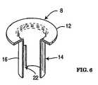
- FIG. 6is a perspective view, partially broken away, of the completed compliant pin.
- FIG. 7is a perspective view of the completed compliant pin.
- FIG. 8is a perspective view of an alternative embodiment of the compliant pin having additional side wall slits.
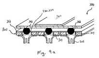
- FIG. 9 ais an enlarged, perspective sectional view of a beam ball grid array (BBGA) system of the present invention and its attachment to a device, package, or module;
- BBGAbeam ball grid array
- FIG. 9 bis an elevational sectional view of the contact system of FIG. 9 a;
- FIG. 9 cis a generic sectional view showing contact arm deformation in accordance with the embodiment shown in FIGS. 9 a and 9 b;
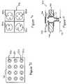
- FIG. 9 dis a plan view of a contact element array as shown in FIG. 9 a;
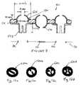
- FIG. 9 eis a plan view of alternative contact element designs
- FIG. 10is a cross-sectional view of a land grid array (LGA) system and its attachment to first and second devices according to a preferred embodiment of the present invention
- FIG. 11is an elevational sectional view of a LGA contact system according to another preferred embodiment of the present invention.
- FIGS. 12 a–dare perspective view of different contact element designs
- FIG. 13is an exploded perspective views of a connector according to another preferred embodiment of the present invention.
- FIG. 14is a flowchart depicting a process for creating a connector according to a preferred embodiment of the present invention.
- the present inventionprovides an interposer 1 and a method for making the interposer 1 .
- the interposer 1includes a printed circuit board (PCB) 6 and a plurality of compliant pins 8 adhered to a first surface thereof.
- a layer 12which includes a plurality of contact elements 20 including elastic portions or contact arms 24 , is adhered to a second surface of the PCB 6 .
- Vias 4provide an electrical path between the compliant pins 8 and the layer 12 .
- the interposer 1is suitable for connecting first and second devices 60 , 62 together.
- the compliant pins 8are preferably fabricated from a single sheet of conductive and resilient material such as copper (Cu) or beryllium copper (BeCu). Alternatively, brass, phosphorous bronze or other suitable alloys may also be used. Referring to FIG. 2 , a sheet 10 of conductive and resilient material is shown. Although the sheet 10 is shown as being configured in a generally square shape having a certain thickness, those of skill in the art should realize that this is for convenience of explanation and the shape and/or thickness of the sheet 10 will vary depending upon the particular application and the desired physical characteristics of the compliant pin. Such physical characteristics, for example, may include the impedance of the compliant pin, the desired normal force to be applied by the compliant pin and the working range of the compliant pin. The length and width of the compliant pin, as well as the distance between adjacent ones of the pins (i.e. the pitch) are also factors used in the selection of material composition and thickness.
- FIG. 3a partial view of the sheet 10 , representative of each of circular areas depicted in dashed lines in FIG. 2 , is shown. This portion of the sheet 10 corresponds to the areas in which each of the compliant pins 8 are formed.
- the sheet 10is drawn to form one or more cavities using a deep drawing process as shown in FIG. 4 .
- Deep drawingis a well known process to those of skill in the metallurgical arts and, therefore, a description of the process will not be set forth in detail hereinafter. Generally, however, deep drawing selectively stretches a sheet of material to form a desired three-dimensional shape.
- the cylindrical shape as shown in FIG. 4 and the subsequent Figuresis for example only and the shape may be any shape desired for the particular application.
- the body 14may be substantially rectilinear in shape, or may be drawn much deeper or much more shallow than shown.
- the body 14generally comprises one or more side walls 16 and a bottom 18 .
- the body 14 shown in the figuresis substantially cylindrical and slightly tapered toward the bottom to allow easier insertion, and comprises a single continuous wall 16 .
- the body 14could also be a cubic or other three-dimensional shape, so that there may be a plurality of side walls 16 .
- a bottom 18is shown, a deep drawing process may be used such that there is no bottom 18 to the body 14 .
- the bottom 18may optionally be removed as shown in FIG. 5 .
- This stepis preferably used when it is desired to have a compliant pin with an extended mechanical operating range. As such, removing the bottom 18 from the body 14 would have certain operational advantages, although this step is optional and is not required for the compliant pin 8 to operate properly.
- At least one slitis made in the wall 16 to form an opening 22 .
- at least one opening 22is formed in the wall 16
- any suitable number of openingscan be formed, depending on the required insertion force and normal spring force desired.
- an additional opening 23is added to provide added compliancy in the pin 8 .
- the pins 8may be provided without openings.
- the completed sheet 10 with compliant pins 8is attached to the PCB 6 to form the interposer 1 , preferably using a suitable bonding adhesive such as polyimide, epoxy, silver-filled glass adhesive or other adhesive including pressure sensitive and heat cured adhesives.
- a suitable bonding adhesivesuch as polyimide, epoxy, silver-filled glass adhesive or other adhesive including pressure sensitive and heat cured adhesives.
- one or more of the compliant pins 8are then singulated, preferably using known etching techniques. Alternatively, mechanical or electrical techniques of singulating the compliant pins 8 may be used.
- the contact elements 20may be formed from a conductive material sheet by a stamping, etching or other suitable process.
- the contact elements 20 and layer 12can be deposited by a CVD process, electro plating, sputtering, PVD, or other conventional metal film deposition techniques.
- electroplate the interposer 1it is preferable to electroplate the interposer 1 to ensure electrical continuity between the pins 8 , contact elements 20 , and vias 4 .
- the arms 24are suitable for connection with land contacts 40 of the first device 60 .
- the first device 60may represent a packaged electronic component having land grid array (LGA) contacts, or alternatively, may represent any component having one or more substantially flat contact areas.
- LGAland grid array
- the arms 24are capable of significant elastic bending to allow good contact between mating surfaces even if such surfaces are not entirely planar. Further, by providing alternative configurations of the arms, a variety of device types may be interfaced.
- the interposer 1may also be selectively connected to the second device 62 using the compliant pins 8 .
- the second device 62 as shownmay represent a second PCB, a cable connector or other components.
- the compliant pins 8are connectable with plated through holes 42 of the second device 62 .
- the compliant pins 8provide a spring force radially outwardly against the perimeter of the holes 42 to removably retain the pins 8 in the holes.
- the removable connectionmay be made permanent through use of solder, adhesive bonding or other known bonding methods. If openings 22 , 23 are not provided in the pins 8 , it is preferable that the interposer be assembled using solder to attach the pins to the holes 42 .
- the sheet 10is preferably Copper (Cu) or a suitable Copper Alloy.
- the interposer 1may be connected with cables or other electronic devices using the compliant pins 8 which are scalable and may be sized to accommodate a variety of electronic devices of different sizes and applications.
- solder balls 302provide a method of establishing an electrical contact between a device, packages, or module 360 , and a carrier/interposer 301 .
- the solder balls 302are shown positioned within through plated vias 304 that have been fabricated in the interposer 301 by printed circuit techniques.
- the solder balls 302are given elasticity by virtue of their suspension upon contact elements 320 , which include flexible contact arms 324 formed as part of a layer 312 .
- the contact arms 320cradle the solder ball 302 and provide a spring-like support, as shown in FIG. 9 c , which is a generic representation of the embodiments of FIGS. 9 a and 9 b.
- FIG. 9 dAn array of the contact elements 320 fabricated in the layer 312 , is shown in FIG. 9 d .
- Different design patterns for the contact elements 320are respectively illustrated by elements 320 a , 320 b , 320 c , and 320 d in FIG. 9 e.
- FIG. 10is a cross-sectional view of a Beam Land Grid Array (BLGA) interposer 401 according to another preferred embodiment of the present invention.
- the BLGA interposer 401includes a carrier layer 406 , which is preferably a PCB.
- a contact element 420includes an array of elastic arms 424 that extend out of the plane of the carrier layer 406 .
- a through plated via 404connects the arms 424 to a compliant pin 408 of the type described above.
- the angle, thickness, and number of the arms 424can be readily changed to provide specific design features such as contact force, current carrying capacity, and contact resistance.
- the interposer 401is suitable for connection to a first device 460 and second device 462 .
- the elements 420can have shapes similar to the elements 320 a–d in FIG. 9 e.
- FIG. 11shows a cross-sectional view of an interposer 501 in accordance with another preferred embodiment of the invention, including exemplary dimensions for the size of the portions of elements 520 .
- the spacing between the distal ends of arms 524is 5 mils.
- the distance from the surface of a carrier layer 506 to a top portion of the arms 524is 10 mils.
- the width of a through hole of the interposer 501can be on the order of 10 mils.
- the width of the contact element 520 from the outer edge of one base portion to the outer edge of the other base portionis 16 mils. Contacts of this size can be formed in accordance with the method of the invention as described below, allowing connectors with a pitch well below 50 mils, and on the order of 20 mils or less.
- Pins 508have a length of 20 mils, although shorter or longer lengths may be provided. It is noted that these dimensions are merely exemplary of what can be achieved with the present invention and one skilled in the art will understand from the present disclosure that a contact element with larger or smaller dimensions could be formed. Further, although the pins 508 and the elements 520 are shown sized similarly, one skilled in the art will recognize that the scale of the pins 508 and the elements 520 may be dissimilar to a small or great extent depending on the particular application.
- the interposer 501includes opposing contact elements 540 adjacent to alternating pins 508 on one of the sides of the interposer 501 . This configuration allows the interposer 501 to interface with a device 570 having both plated through holes 542 and land contacts 540 , or similar types of contacts, on a single surface.
- the following mechanical propertiescan be specifically engineered for contact elements or pins, to achieve certain desired operational characteristics.
- the contact force for each contact element and pincan be selected to ensure either a low resistance connection for some contact elements and/or pins, or a low overall contact force for the connector.
- the elastic working range of each contact element and pincan be varied.
- the vertical height of each contact element and pincan be varied.
- the pitch or horizontal dimensions of the contact elements and pinscan be varied.
- a plurality of contact element designs 620 a , 620 b , 620 c , 620 dare shown for either a BBGA or a BLGA system.
- these contact elementscan be either stamped or etched into a spring-like structure, and can be heat treated before or after forming, if required, based on the material selected and the particular application.
- FIG. 13is an exploded perspective view showing the assembly of a connector 701 according to another preferred embodiment of the present invention.
- the connectorincludes a first sheet 710 including compliant pins 708 that is positioned on a first major surface of a dielectric substrate 706 .
- An array of contact elements 720 having contact arms 724are formed from a second sheet 712 that is positioned on a second major surface of a dielectric substrate 706 .
- the contact elements 720 and the pins 708are preferably aligned with respective holes 730 formed in the substrate 706 .
- Metal traces or vias 704are preferably provided in the holes 730 to connect the contact elements 720 from the second major surface to the pins 708 from the first major surface.
- FIG. 13shows the connector 701 during an intermediate step in the manufacturing process for forming the connector. Therefore, the array of contact elements 720 and the array of compliant pins 708 are shown as being joined together on the respective sheets of metal or metallic material 712 , 710 from which they are formed. In the subsequent manufacturing steps, the unwanted portions of the metal sheets 710 , 712 are removed, so that the contact elements 720 and pins 708 are isolated (i.e., singulated) as needed. For example, the metal sheets 710 , 712 can be masked and etched to singulate some or all of the contact elements 720 and/or compliant pins 708 from one another.
- the connector 701 of FIG. 13is formed as follows. First, the dielectric substrate 706 including conductive paths between the top surface and the bottom surface is provided. The conductive paths are preferably in the form of the through plated traces or vias 704 . Alternatively, other types of vias such as those shown in FIG. 1 may be used.
- the conductive metal sheet 712 or a multilayer metal sheetis patterned to form an array of contact elements 720 including a base portion and one or more elastic portions or arms 724 .
- the contact elements 720including the contact arms 724 , can be formed by etching, stamping, and/or other means.
- the metal sheet 712is attached to the second major surface of the dielectric substrate 706 .
- the sheet 710 with compliant pins 708that is formed as described above with reference to FIGS. 2–9 , is attached to the first major surface of the dielectric substrate 706 .
- the metal sheets 710 , 712can then be patterned to remove unwanted metal from the sheets so that the contact elements 720 and/or compliant pins 708 are isolated from each other (i.e., singulated) as needed.
- the metal sheets 710 , 712can be patterned by etching, scribing, stamping, and/or other known methods.
- the pins 708 and/or contact elements 720can be singulated without attaching their respective sheets to the substrate. The singulated pins 708 or contact elements 720 may then be individually installed.
- conductive traces 704are formed in the through holes 730 and also on the surface of the dielectric substrate 706 in a ring-shaped pattern 732 encircling each plated through hole. While the conductive rings 732 can be provided to enhance the electrical connection among the contact elements 720 , the pins 708 and the conductive traces formed in the dielectric layer 706 , the conductive rings 732 are not required components of the connector 701 . In another embodiment, the connector 701 can be formed by using a dielectric substrate including through holes that are not plated.
- the entire connector 701may be plated to form conductive traces in the through holes 730 , connecting the contact elements 720 to the compliant pins 708 on the other side of the dielectric substrate.
- a connector according to the present inventioncould be used as an interposer, a PCB connector, or could be formed as a PCB.
- the scalability of the present inventionis not limited, and can be easily customized for particular applications.
- the methodincludes providing a printed circuit board (PCB) having first and second surfaces (step 202 ).
- the methodfurther includes deep drawing a first conductive material sheet to form a plurality of bodies (step 204 ), optionally removing the closed ends of the bodies (step 206 ), and forming an opening in at least a portion of a side wall of each of the bodies to create compliant pins (step 208 ).
- the first conductive material sheetis attached to the first surface of the PCB (step 210 ).
- a plurality of contact elements having at least one elastic portionare formed from a second conductive material sheet ( 212 ).
- the second conductive material sheetis attached to the second surface of the PCB (step 214 ).
- the compliant pins and the contact elementsare singulated (step 216 ).
- some of the compliant pins and/or contact elementsmay remain non-singulated as required by the particular application.
- the methodalso includes connecting the contact elements to the compliant pins using vias (step 218 ).
Landscapes
- Coupling Device And Connection With Printed Circuit (AREA)
Abstract
Description
Claims (27)
Priority Applications (2)
| Application Number | Priority Date | Filing Date | Title |
|---|---|---|---|
| US10/894,608US7090503B2 (en) | 2004-03-19 | 2004-07-20 | Interposer with compliant pins |
| US11/487,378US7354276B2 (en) | 2004-07-20 | 2006-07-17 | Interposer with compliant pins |
Applications Claiming Priority (2)
| Application Number | Priority Date | Filing Date | Title |
|---|---|---|---|
| US55471904P | 2004-03-19 | 2004-03-19 | |
| US10/894,608US7090503B2 (en) | 2004-03-19 | 2004-07-20 | Interposer with compliant pins |
Related Child Applications (1)
| Application Number | Title | Priority Date | Filing Date |
|---|---|---|---|
| US11/487,378ContinuationUS7354276B2 (en) | 2004-07-20 | 2006-07-17 | Interposer with compliant pins |
Publications (2)
| Publication Number | Publication Date |
|---|---|
| US20050208787A1 US20050208787A1 (en) | 2005-09-22 |
| US7090503B2true US7090503B2 (en) | 2006-08-15 |
Family
ID=34986933
Family Applications (1)
| Application Number | Title | Priority Date | Filing Date |
|---|---|---|---|
| US10/894,608Expired - LifetimeUS7090503B2 (en) | 2004-03-19 | 2004-07-20 | Interposer with compliant pins |
Country Status (1)
| Country | Link |
|---|---|
| US (1) | US7090503B2 (en) |
Cited By (21)
| Publication number | Priority date | Publication date | Assignee | Title |
|---|---|---|---|---|
| US20050204538A1 (en)* | 2004-03-19 | 2005-09-22 | Epic Technology Inc. | Contact and method for making same |
| US7354276B2 (en) | 2004-07-20 | 2008-04-08 | Neoconix, Inc. | Interposer with compliant pins |
| US7357644B2 (en) | 2005-12-12 | 2008-04-15 | Neoconix, Inc. | Connector having staggered contact architecture for enhanced working range |
| US7371073B2 (en) | 2003-04-11 | 2008-05-13 | Neoconix, Inc. | Contact grid array system |
| US7383632B2 (en) | 2004-03-19 | 2008-06-10 | Neoconix, Inc. | Method for fabricating a connector |
| US20080204060A1 (en)* | 2004-10-26 | 2008-08-28 | Song Byoung-Hak | Vertical-Type Electric Contactor And Manufacture Method Thereof |
| US7587817B2 (en) | 2003-04-11 | 2009-09-15 | Neoconix, Inc. | Method of making electrical connector on a flexible carrier |
| US7597561B2 (en) | 2003-04-11 | 2009-10-06 | Neoconix, Inc. | Method and system for batch forming spring elements in three dimensions |
| US7628617B2 (en) | 2003-06-11 | 2009-12-08 | Neoconix, Inc. | Structure and process for a contact grid array formed in a circuitized substrate |
| US7758351B2 (en) | 2003-04-11 | 2010-07-20 | Neoconix, Inc. | Method and system for batch manufacturing of spring elements |
| US7914296B1 (en)* | 2010-01-05 | 2011-03-29 | Exatron, Inc. | Interconnecting assembly with conductive lever portions on a support film |
| US7989945B2 (en) | 2003-12-08 | 2011-08-02 | Neoconix, Inc. | Spring connector for making electrical contact at semiconductor scales |
| US20110256743A1 (en)* | 2010-04-20 | 2011-10-20 | Tyco Electronics Corporation | Interposer connector assembly |
| US8519274B2 (en) | 2011-03-08 | 2013-08-27 | International Business Machines Corporation | Pin that inserts into a circuit board hole |
| US8584353B2 (en) | 2003-04-11 | 2013-11-19 | Neoconix, Inc. | Method for fabricating a contact grid array |
| US8641428B2 (en) | 2011-12-02 | 2014-02-04 | Neoconix, Inc. | Electrical connector and method of making it |
| US9680273B2 (en) | 2013-03-15 | 2017-06-13 | Neoconix, Inc | Electrical connector with electrical contacts protected by a layer of compressible material and method of making it |
| US11211728B2 (en) | 2019-01-14 | 2021-12-28 | Amphenol Corporation | Midboard cable terminology assembly |
| US11404811B2 (en) | 2019-01-14 | 2022-08-02 | Amphenol Corporation | Small form factor interposer |
| US11476619B2 (en) | 2018-07-20 | 2022-10-18 | Fci Usa Llc | High frequency connector with kick-out |
| US11670879B2 (en) | 2020-01-28 | 2023-06-06 | Fci Usa Llc | High frequency midboard connector |
Families Citing this family (3)
| Publication number | Priority date | Publication date | Assignee | Title |
|---|---|---|---|---|
| US7137827B2 (en)* | 2003-11-17 | 2006-11-21 | International Business Machines Corporation | Interposer with electrical contact button and method |
| US7491101B2 (en)* | 2004-06-17 | 2009-02-17 | Illinois Tool Works Inc. | Self-locking wire terminal and shape memory wire termination system |
| US11862901B2 (en) | 2020-12-15 | 2024-01-02 | Teradyne, Inc. | Interposer |
Citations (148)
| Publication number | Priority date | Publication date | Assignee | Title |
|---|---|---|---|---|
| US3543587A (en) | 1967-10-07 | 1970-12-01 | Tokyo Keiki Kk | Gyroscopic instrument |
| US3634807A (en) | 1969-03-28 | 1972-01-11 | Siemens Ag | Detachable electrical contact arrangement |
| US3670409A (en) | 1970-11-19 | 1972-06-20 | Gte Automatic Electric Lab Inc | Planar receptacle |
| US4175810A (en) | 1976-11-22 | 1979-11-27 | Augat Inc. | Electrical interconnection boards with lead sockets mounted therein and method for making same |
| US4548451A (en) | 1984-04-27 | 1985-10-22 | International Business Machines Corporation | Pinless connector interposer and method for making the same |
| US4657336A (en) | 1985-12-18 | 1987-04-14 | Gte Products Corporation | Socket receptacle including overstress protection means for mounting electrical devices on printed circuit boards |
| US4893172A (en) | 1987-01-19 | 1990-01-09 | Hitachi, Ltd. | Connecting structure for electronic part and method of manufacturing the same |
| US4998885A (en) | 1989-10-27 | 1991-03-12 | International Business Machines Corporation | Elastomeric area array interposer |
| US5135403A (en) | 1991-06-07 | 1992-08-04 | Amp Incorporated | Solderless spring socket for printed circuit board |
| US5148266A (en) | 1990-09-24 | 1992-09-15 | Ist Associates, Inc. | Semiconductor chip assemblies having interposer and flexible lead |
| US5152695A (en) | 1991-10-10 | 1992-10-06 | Amp Incorporated | Surface mount electrical connector |
| US5173055A (en) | 1991-08-08 | 1992-12-22 | Amp Incorporated | Area array connector |
| US5199879A (en) | 1992-02-24 | 1993-04-06 | International Business Machines Corporation | Electrical assembly with flexible circuit |
| US5228861A (en) | 1992-06-12 | 1993-07-20 | Amp Incorporated | High density electrical connector system |
| US5257950A (en) | 1991-07-17 | 1993-11-02 | The Whitaker Corporation | Filtered electrical connector |
| US5292558A (en) | 1991-08-08 | 1994-03-08 | University Of Texas At Austin, Texas | Process for metal deposition for microelectronic interconnections |
| US5299939A (en) | 1992-03-05 | 1994-04-05 | International Business Machines Corporation | Spring array connector |
| US5358411A (en) | 1993-08-09 | 1994-10-25 | The Whitaker Corporation | Duplex plated epsilon compliant beam contact and interposer |
| US5366380A (en)* | 1989-06-13 | 1994-11-22 | General Datacomm, Inc. | Spring biased tapered contact elements for electrical connectors and integrated circuit packages |
| US5468655A (en) | 1994-10-31 | 1995-11-21 | Motorola, Inc. | Method for forming a temporary attachment between a semiconductor die and a substrate using a metal paste comprising spherical modules |
| US5483741A (en) | 1993-09-03 | 1996-01-16 | Micron Technology, Inc. | Method for fabricating a self limiting silicon based interconnect for testing bare semiconductor dice |
| WO1996002068A1 (en) | 1994-07-07 | 1996-01-25 | Tessera, Inc. | Microelectronic mounting with multiple lead deformation |
| US5509814A (en) | 1993-06-01 | 1996-04-23 | Itt Corporation | Socket contact for mounting in a hole of a device |
| US5530288A (en) | 1994-10-12 | 1996-06-25 | International Business Machines Corporation | Passive interposer including at least one passive electronic component |
| US5532612A (en) | 1994-07-19 | 1996-07-02 | Liang; Louis H. | Methods and apparatus for test and burn-in of integrated circuit devices |
| US5590460A (en) | 1994-07-19 | 1997-01-07 | Tessera, Inc. | Method of making multilayer circuit |
| US5593903A (en) | 1996-03-04 | 1997-01-14 | Motorola, Inc. | Method of forming contact pads for wafer level testing and burn-in of semiconductor dice |
| US5629837A (en) | 1995-09-20 | 1997-05-13 | Oz Technologies, Inc. | Button contact for surface mounting an IC device to a circuit board |
| US5632631A (en) | 1994-06-07 | 1997-05-27 | Tessera, Inc. | Microelectronic contacts with asperities and methods of making same |
| WO1997044859A1 (en) | 1996-05-24 | 1997-11-27 | Tessera, Inc. | Connectors for microelectronic elements |
| US5751556A (en) | 1996-03-29 | 1998-05-12 | Intel Corporation | Method and apparatus for reducing warpage of an assembly substrate |
| US5772451A (en) | 1993-11-16 | 1998-06-30 | Form Factor, Inc. | Sockets for electronic components and methods of connecting to electronic components |
| US5791911A (en) | 1996-10-25 | 1998-08-11 | International Business Machines Corporation | Coaxial interconnect devices and methods of making the same |
| US5802699A (en) | 1994-06-07 | 1998-09-08 | Tessera, Inc. | Methods of assembling microelectronic assembly with socket for engaging bump leads |
| US5842273A (en) | 1996-01-26 | 1998-12-01 | Hewlett-Packard Company | Method of forming electrical interconnects using isotropic conductive adhesives and connections formed thereby |
| US5860585A (en) | 1996-05-31 | 1999-01-19 | Motorola, Inc. | Substrate for transferring bumps and method of use |
| US5896038A (en) | 1996-11-08 | 1999-04-20 | W. L. Gore & Associates, Inc. | Method of wafer level burn-in |
| US5967797A (en) | 1997-09-24 | 1999-10-19 | Teledyne Industries, Inc. | High density multi-pin connector with solder points |
| US5980335A (en) | 1998-03-27 | 1999-11-09 | Molex Incorporated | Electrical terminal |
| US5989994A (en) | 1998-12-29 | 1999-11-23 | Advantest Corp. | Method for producing contact structures |
| JP2000011443A (en) | 1998-04-21 | 2000-01-14 | Nec Corp | Optical module device, combined prism using it, and forming method thereof |
| US6019611A (en) | 1998-02-12 | 2000-02-01 | Hon Hai Precision Ind. Co., Ltd. | Land grid array assembly and related contact |
| US6031282A (en) | 1998-08-27 | 2000-02-29 | Advantest Corp. | High performance integrated circuit chip package |
| US6029344A (en) | 1993-11-16 | 2000-02-29 | Formfactor, Inc. | Composite interconnection element for microelectronic components, and method of making same |
| US6032356A (en) | 1993-11-16 | 2000-03-07 | Formfactor. Inc. | Wafer-level test and burn-in, and semiconductor process |
| US6042387A (en) | 1998-03-27 | 2000-03-28 | Oz Technologies, Inc. | Connector, connector system and method of making a connector |
| US6063640A (en) | 1997-03-18 | 2000-05-16 | Fujitsu Limited | Semiconductor wafer testing method with probe pin contact |
| US6083837A (en) | 1996-12-13 | 2000-07-04 | Tessera, Inc. | Fabrication of components by coining |
| US6133534A (en) | 1991-11-29 | 2000-10-17 | Hitachi Chemical Company, Ltd. | Wiring board for electrical tests with bumps having polymeric coating |
| US6146151A (en) | 1999-08-18 | 2000-11-14 | Hon Hai Precision Ind. Co., Ltd. | Method for forming an electrical connector and an electrical connector obtained by the method |
| US6156484A (en) | 1997-11-07 | 2000-12-05 | International Business Machines Corporation | Gray scale etching for thin flexible interposer |
| US6184699B1 (en) | 1995-06-07 | 2001-02-06 | Xerox Corporation | Photolithographically patterned spring contact |
| US6196852B1 (en)* | 1997-04-02 | 2001-03-06 | Siemens Nixdorf Informationssysteme Aktiengesellschaft | Contact arrangement |
| US6200143B1 (en) | 1998-01-09 | 2001-03-13 | Tessera, Inc. | Low insertion force connector for microelectronic elements |
| US6204065B1 (en) | 1997-03-27 | 2001-03-20 | Ngk Insulators, Ltd. | Conduction assist member and manufacturing method of the same |
| US6208157B1 (en) | 1997-08-22 | 2001-03-27 | Micron Technology, Inc. | Method for testing semiconductor components |
| US6221750B1 (en) | 1998-10-28 | 2001-04-24 | Tessera, Inc. | Fabrication of deformable leads of microelectronic elements |
| US6224392B1 (en) | 1998-12-04 | 2001-05-01 | International Business Machines Corporation | Compliant high-density land grid array (LGA) connector and method of manufacture |
| US20010001080A1 (en) | 1999-07-30 | 2001-05-10 | Eldridge Benjamin N. | Interconnect assemblies and methods |
| US6250933B1 (en) | 2000-01-20 | 2001-06-26 | Advantest Corp. | Contact structure and production method thereof |
| US6255727B1 (en) | 1999-08-03 | 2001-07-03 | Advantest Corp. | Contact structure formed by microfabrication process |
| US6263566B1 (en) | 1999-05-03 | 2001-07-24 | Micron Technology, Inc. | Flexible semiconductor interconnect fabricated by backslide thinning |
| JP2001203435A (en) | 2000-01-21 | 2001-07-27 | Ibiden Co Ltd | Connection structure of ball grid array type package |
| US6293808B1 (en) | 1999-09-30 | 2001-09-25 | Ngk Insulators, Ltd. | Contact sheet |
| US6293806B1 (en)* | 2000-02-02 | 2001-09-25 | Hon Hai Precision Ind. Co., Ltd. | Electrical connector with improved terminals for electrically connecting to a circuit board |
| US6297164B1 (en) | 1998-11-30 | 2001-10-02 | Advantest Corp. | Method for producing contact structures |
| US6298552B1 (en) | 2000-02-10 | 2001-10-09 | Hon Hai Precision Ind. Co., Ltd. | Method for making socket connector |
| US6306752B1 (en) | 1998-09-15 | 2001-10-23 | Tessera, Inc. | Connection component and method of making same |
| US6335210B1 (en) | 1999-12-17 | 2002-01-01 | International Business Machines Corporation | Baseplate for chip burn-in and/of testing, and method thereof |
| US6336269B1 (en) | 1993-11-16 | 2002-01-08 | Benjamin N. Eldridge | Method of fabricating an interconnection element |
| US6337575B1 (en) | 1998-12-23 | 2002-01-08 | Micron Technology, Inc. | Methods of testing integrated circuitry, methods of forming tester substrates, and circuitry testing substrates |
| US20020011859A1 (en) | 1993-12-23 | 2002-01-31 | Kenneth R. Smith | Method for forming conductive bumps for the purpose of contrructing a fine pitch test device |
| WO2002013253A1 (en) | 2000-08-03 | 2002-02-14 | David Frank Moore | Microconnectors and method for their production |
| US6361328B1 (en)* | 1999-08-03 | 2002-03-26 | Framatome Connectors International | Surface-mounted low profile connector |
| US6373267B1 (en) | 1997-05-30 | 2002-04-16 | Ando Electric Company | Ball grid array-integrated circuit testing device |
| US20020055282A1 (en) | 2000-11-09 | 2002-05-09 | Eldridge Benjamin N. | Electronic components with plurality of contoured microelectronic spring contacts |
| US20020058356A1 (en) | 1998-04-16 | 2002-05-16 | Yoichi Oya | Semiconductor package and mount board, and mounting method using the same |
| US6392534B1 (en) | 1996-08-22 | 2002-05-21 | Kenneth E. Flick | Remote control system for a vehicle having a data communications bus and related methods |
| US6392524B1 (en) | 2000-06-09 | 2002-05-21 | Xerox Corporation | Photolithographically-patterned out-of-plane coil structures and method of making |
| US6399900B1 (en) | 1999-04-30 | 2002-06-04 | Advantest Corp. | Contact structure formed over a groove |
| US6397460B1 (en) | 1999-03-10 | 2002-06-04 | Micron Technology, Inc. | Electrical connector |
| US6402526B1 (en)* | 2000-11-03 | 2002-06-11 | Delphi Technologies, Inc. | Microelectronic contact assembly |
| US6409521B1 (en) | 1997-05-06 | 2002-06-25 | Gryphics, Inc. | Multi-mode compliant connector and replaceable chip module utilizing the same |
| US20020079120A1 (en) | 1999-08-30 | 2002-06-27 | Steven R. Eskildsen | Implementing micro bgatm assembly techniques for small die |
| US6420661B1 (en) | 1995-09-12 | 2002-07-16 | Tessera, Inc. | Connector element for connecting microelectronic elements |
| US6420884B1 (en) | 1999-01-29 | 2002-07-16 | Advantest Corp. | Contact structure formed by photolithography process |
| US6420789B1 (en) | 2000-05-16 | 2002-07-16 | Micron Technology, Inc. | Ball grid array chip packages having improved testing and stacking characteristics |
| US6437591B1 (en) | 1999-03-25 | 2002-08-20 | Micron Technology, Inc. | Test interconnect for bumped semiconductor components and method of fabrication |
| US6436802B1 (en) | 1998-11-30 | 2002-08-20 | Adoamtest Corp. | Method of producing contact structure |
| US6442039B1 (en) | 1999-12-03 | 2002-08-27 | Delphi Technologies, Inc. | Metallic microstructure springs and method of making same |
| US20020117330A1 (en) | 1993-11-16 | 2002-08-29 | Formfactor, Inc. | Resilient contact structures formed and then attached to a substrate |
| US6452407B2 (en) | 1998-06-19 | 2002-09-17 | Advantest Corp. | Probe contactor and production method thereof |
| US20020129894A1 (en) | 2001-01-08 | 2002-09-19 | Kuo-Chuan Liu | Method for joining and an ultra-high density interconnect |
| US6461892B2 (en) | 2000-01-26 | 2002-10-08 | Tessera, Inc. | Methods of making a connection component using a removable layer |
| US20020146919A1 (en) | 2000-12-29 | 2002-10-10 | Cohn Michael B. | Micromachined springs for strain relieved electrical connections to IC chips |
| US6465748B2 (en) | 2000-07-19 | 2002-10-15 | Yazaki Corporation | Wiring unit |
| US6474997B1 (en) | 1999-09-30 | 2002-11-05 | Ngk Insulators, Ltd. | Contact sheet |
| US20020178331A1 (en) | 1999-04-23 | 2002-11-28 | Beardsley Brent Cameron | Prestaging data into cache in preparation for data transfer operations |
| US6492251B1 (en) | 1999-03-10 | 2002-12-10 | Tessera, Inc. | Microelectronic joining processes with bonding material application |
| US20030003779A1 (en) | 2000-01-20 | 2003-01-02 | Rathburn James J | Flexible compliant interconnect assembly |
| US20030000739A1 (en) | 2001-06-29 | 2003-01-02 | Intel Corporation | Circuit housing clamp and method of manufacture therefor |
| US20030022503A1 (en) | 2001-07-27 | 2003-01-30 | Clements Bradley E. | Method for the fabrication of electrical contacts |
| US6517362B2 (en) | 2000-09-26 | 2003-02-11 | Yukihiro Hirai | Spiral contactor, semiconductor device inspecting apparatus and electronic part using same, and method of manufacturing the same |
| US6520778B1 (en) | 1997-02-18 | 2003-02-18 | Formfactor, Inc. | Microelectronic contact structures, and methods of making same |
| EP0692823B1 (en) | 1994-07-11 | 2003-02-19 | Sun Microsystems, Inc. | Ball grid array package for an integated circuit and method of reducing ground bounce |
| US20030035277A1 (en) | 2001-07-13 | 2003-02-20 | Saputro Stephanus D. | Reducing inductance of a capacitor |
| US6524115B1 (en) | 1999-08-20 | 2003-02-25 | 3M Innovative Properties Company | Compliant interconnect assembly |
| US20030049951A1 (en) | 1998-02-13 | 2003-03-13 | Formfactor, Inc. | Microelectronic contact structures, and methods of making same |
| US6551112B1 (en) | 2002-03-18 | 2003-04-22 | High Connection Density, Inc. | Test and burn-in connector |
| US20030089936A1 (en) | 2001-11-13 | 2003-05-15 | Mccormack Mark Thomas | Structure and method for embedding capacitors in Z-connected multi-chip modules |
| US20030096512A1 (en) | 2001-06-14 | 2003-05-22 | Christopher Cornell | Electrical interconnect device incorporating anisotropically conductive elastomer and flexible circuit |
| US20030099097A1 (en) | 2001-11-27 | 2003-05-29 | Sammy Mok | Construction structures and manufacturing processes for probe card assemblies and packages having wafer level springs |
| US6576485B2 (en) | 1998-11-30 | 2003-06-10 | Advantest Corp. | Contact structure and production method thereof and probe contact assembly using same |
| US20030129866A1 (en) | 2002-01-07 | 2003-07-10 | Romano Linda T. | Spring metal structure with passive-conductive coating on tip |
| US20030147197A1 (en) | 2000-03-15 | 2003-08-07 | Kazuhide Uriu | Multilayer electronic part, multilayer antenna duplexer, and communication apparatus |
| US6604950B2 (en) | 2001-04-26 | 2003-08-12 | Teledyne Technologies Incorporated | Low pitch, high density connector |
| US6612861B2 (en) | 2000-02-14 | 2003-09-02 | Advantest Corp. | Contact structure and production method thereof |
| EP1005086B1 (en) | 1998-11-26 | 2003-09-03 | Shinko Electric Industries Co. Ltd. | Metal foil having bumps, circuit substrate having the metal foil, and semiconductor device having the circuit substrate |
| US6616966B2 (en) | 1998-12-02 | 2003-09-09 | Formfactor, Inc. | Method of making lithographic contact springs |
| US6622380B1 (en) | 2002-02-12 | 2003-09-23 | Micron Technology, Inc. | Methods for manufacturing microelectronic devices and methods for mounting microelectronic packages to circuit boards |
| US6627092B2 (en) | 2001-07-27 | 2003-09-30 | Hewlett-Packard Development Company, L.P. | Method for the fabrication of electrical contacts |
| US20030194832A1 (en) | 2001-09-26 | 2003-10-16 | Lopata John E.. | Power delivery system for integrated circuits utilizing discrete capacitors |
| US6640432B1 (en) | 2000-04-12 | 2003-11-04 | Formfactor, Inc. | Method of fabricating shaped springs |
| US6661247B2 (en) | 1997-09-19 | 2003-12-09 | Fujitsu Limited | Semiconductor testing device |
| US6664131B2 (en) | 1999-07-13 | 2003-12-16 | Micron Technology, Inc. | Method of making ball grid array package with deflectable interconnect |
| US6671947B2 (en) | 1999-06-28 | 2004-01-06 | Intel Corporation | Method of making an interposer |
| US6677245B2 (en) | 1998-11-30 | 2004-01-13 | Advantest Corp. | Contact structure production method |
| US6692263B2 (en) | 2000-10-02 | 2004-02-17 | Alcatel | Spring connector for electrically connecting tracks of a display screen with an electrical circuit |
| US6700072B2 (en) | 1996-12-13 | 2004-03-02 | Tessera, Inc. | Electrical connection with inwardly deformable contacts |
| US6701612B2 (en) | 1993-11-16 | 2004-03-09 | Formfactor, Inc. | Method and apparatus for shaping spring elements |
| US6719569B2 (en) | 2001-10-02 | 2004-04-13 | Ngk Insulators, Ltd. | Contact sheet for providing an electrical connection between a plurality of electronic devices |
| US6730134B2 (en) | 2001-07-02 | 2004-05-04 | Intercon Systems, Inc. | Interposer assembly |
| US6736665B2 (en) | 1998-11-30 | 2004-05-18 | Advantest Corp. | Contact structure production method |
| US6750136B2 (en) | 1998-11-30 | 2004-06-15 | Advantest Corp. | Contact structure production method |
| US20040118603A1 (en) | 2002-12-18 | 2004-06-24 | Chambers Douglas C. | Methods and apparatus for a flexible circuit interposer |
| US20040127073A1 (en) | 2002-12-27 | 2004-07-01 | Ngk Insulators, Ltd. | Contact sheet, method of manufacturing the same and socket including the same |
| US6791171B2 (en) | 2000-06-20 | 2004-09-14 | Nanonexus, Inc. | Systems for testing and packaging integrated circuits |
| US6814587B2 (en) | 2002-10-25 | 2004-11-09 | Hon Hai Precision Ind. Co., Ltd. | Electrical connector with contacts having cooperating contacting portions |
| US6814584B2 (en) | 2001-05-11 | 2004-11-09 | Molex Incorporated | Elastomeric electrical connector |
| US6815961B2 (en) | 1999-07-28 | 2004-11-09 | Nanonexus, Inc. | Construction structures and manufacturing processes for integrated circuit wafer probe card assemblies |
| EP1208241B1 (en) | 2000-04-04 | 2005-01-12 | Fundacao Oswaldo Cruz - Fiocruz | Method and kit for the detection of schistosomiasis through the polymerase chain reaction |
| US6843659B2 (en) | 2002-11-22 | 2005-01-18 | Hon Hai Precision Ind. Co., Ltd. | Electrical connector having terminals with reinforced interference portions |
| US6847101B2 (en) | 1995-10-31 | 2005-01-25 | Tessera, Inc. | Microelectronic package having a compliant layer with bumped protrusions |
| US6848173B2 (en) | 1994-07-07 | 2005-02-01 | Tessera, Inc. | Microelectric packages having deformed bonded leads and methods therefor |
| US6857880B2 (en) | 2001-11-09 | 2005-02-22 | Tomonari Ohtsuki | Electrical connector |
| US6881070B2 (en) | 2003-05-27 | 2005-04-19 | Molex Incorporated | LGA connector and terminal thereof |
| US20050099193A1 (en) | 2003-11-07 | 2005-05-12 | Jeff Burgess | Electronic component/interface interposer |
| US6916181B2 (en)* | 2003-06-11 | 2005-07-12 | Neoconix, Inc. | Remountable connector for land grid array packages |
Family Cites Families (1)
| Publication number | Priority date | Publication date | Assignee | Title |
|---|---|---|---|---|
| US20030049551A1 (en)* | 2001-09-07 | 2003-03-13 | Xerox Corporation | Blue diode laser sensitive photoreceptor |
- 2004
- 2004-07-20USUS10/894,608patent/US7090503B2/ennot_activeExpired - Lifetime
Patent Citations (157)
| Publication number | Priority date | Publication date | Assignee | Title |
|---|---|---|---|---|
| US3543587A (en) | 1967-10-07 | 1970-12-01 | Tokyo Keiki Kk | Gyroscopic instrument |
| US3634807A (en) | 1969-03-28 | 1972-01-11 | Siemens Ag | Detachable electrical contact arrangement |
| US3670409A (en) | 1970-11-19 | 1972-06-20 | Gte Automatic Electric Lab Inc | Planar receptacle |
| US4175810A (en) | 1976-11-22 | 1979-11-27 | Augat Inc. | Electrical interconnection boards with lead sockets mounted therein and method for making same |
| US4548451A (en) | 1984-04-27 | 1985-10-22 | International Business Machines Corporation | Pinless connector interposer and method for making the same |
| US4657336A (en) | 1985-12-18 | 1987-04-14 | Gte Products Corporation | Socket receptacle including overstress protection means for mounting electrical devices on printed circuit boards |
| US4893172A (en) | 1987-01-19 | 1990-01-09 | Hitachi, Ltd. | Connecting structure for electronic part and method of manufacturing the same |
| US5366380A (en)* | 1989-06-13 | 1994-11-22 | General Datacomm, Inc. | Spring biased tapered contact elements for electrical connectors and integrated circuit packages |
| US4998885A (en) | 1989-10-27 | 1991-03-12 | International Business Machines Corporation | Elastomeric area array interposer |
| US5148266A (en) | 1990-09-24 | 1992-09-15 | Ist Associates, Inc. | Semiconductor chip assemblies having interposer and flexible lead |
| US5135403A (en) | 1991-06-07 | 1992-08-04 | Amp Incorporated | Solderless spring socket for printed circuit board |
| US5257950A (en) | 1991-07-17 | 1993-11-02 | The Whitaker Corporation | Filtered electrical connector |
| US5292558A (en) | 1991-08-08 | 1994-03-08 | University Of Texas At Austin, Texas | Process for metal deposition for microelectronic interconnections |
| US5173055A (en) | 1991-08-08 | 1992-12-22 | Amp Incorporated | Area array connector |
| US5152695A (en) | 1991-10-10 | 1992-10-06 | Amp Incorporated | Surface mount electrical connector |
| US6133534A (en) | 1991-11-29 | 2000-10-17 | Hitachi Chemical Company, Ltd. | Wiring board for electrical tests with bumps having polymeric coating |
| US5199879A (en) | 1992-02-24 | 1993-04-06 | International Business Machines Corporation | Electrical assembly with flexible circuit |
| US5299939A (en) | 1992-03-05 | 1994-04-05 | International Business Machines Corporation | Spring array connector |
| US5228861A (en) | 1992-06-12 | 1993-07-20 | Amp Incorporated | High density electrical connector system |
| US5509814A (en) | 1993-06-01 | 1996-04-23 | Itt Corporation | Socket contact for mounting in a hole of a device |
| US5358411A (en) | 1993-08-09 | 1994-10-25 | The Whitaker Corporation | Duplex plated epsilon compliant beam contact and interposer |
| US5483741A (en) | 1993-09-03 | 1996-01-16 | Micron Technology, Inc. | Method for fabricating a self limiting silicon based interconnect for testing bare semiconductor dice |
| US6032356A (en) | 1993-11-16 | 2000-03-07 | Formfactor. Inc. | Wafer-level test and burn-in, and semiconductor process |
| US20020117330A1 (en) | 1993-11-16 | 2002-08-29 | Formfactor, Inc. | Resilient contact structures formed and then attached to a substrate |
| US5772451A (en) | 1993-11-16 | 1998-06-30 | Form Factor, Inc. | Sockets for electronic components and methods of connecting to electronic components |
| US6029344A (en) | 1993-11-16 | 2000-02-29 | Formfactor, Inc. | Composite interconnection element for microelectronic components, and method of making same |
| US6701612B2 (en) | 1993-11-16 | 2004-03-09 | Formfactor, Inc. | Method and apparatus for shaping spring elements |
| US6336269B1 (en) | 1993-11-16 | 2002-01-08 | Benjamin N. Eldridge | Method of fabricating an interconnection element |
| US20020011859A1 (en) | 1993-12-23 | 2002-01-31 | Kenneth R. Smith | Method for forming conductive bumps for the purpose of contrructing a fine pitch test device |
| US5802699A (en) | 1994-06-07 | 1998-09-08 | Tessera, Inc. | Methods of assembling microelectronic assembly with socket for engaging bump leads |
| US5934914A (en) | 1994-06-07 | 1999-08-10 | Tessera, Inc. | Microelectronic contacts with asperities and methods of making same |
| US6205660B1 (en) | 1994-06-07 | 2001-03-27 | Tessera, Inc. | Method of making an electronic contact |
| US5812378A (en) | 1994-06-07 | 1998-09-22 | Tessera, Inc. | Microelectronic connector for engaging bump leads |
| US5632631A (en) | 1994-06-07 | 1997-05-27 | Tessera, Inc. | Microelectronic contacts with asperities and methods of making same |
| US6848173B2 (en) | 1994-07-07 | 2005-02-01 | Tessera, Inc. | Microelectric packages having deformed bonded leads and methods therefor |
| WO1996002068A1 (en) | 1994-07-07 | 1996-01-25 | Tessera, Inc. | Microelectronic mounting with multiple lead deformation |
| EP0692823B1 (en) | 1994-07-11 | 2003-02-19 | Sun Microsystems, Inc. | Ball grid array package for an integated circuit and method of reducing ground bounce |
| US5590460A (en) | 1994-07-19 | 1997-01-07 | Tessera, Inc. | Method of making multilayer circuit |
| US5532612A (en) | 1994-07-19 | 1996-07-02 | Liang; Louis H. | Methods and apparatus for test and burn-in of integrated circuit devices |
| US5530288A (en) | 1994-10-12 | 1996-06-25 | International Business Machines Corporation | Passive interposer including at least one passive electronic component |
| US5468655A (en) | 1994-10-31 | 1995-11-21 | Motorola, Inc. | Method for forming a temporary attachment between a semiconductor die and a substrate using a metal paste comprising spherical modules |
| US6264477B1 (en) | 1995-06-07 | 2001-07-24 | Xerox Corporation | Photolithographically patterned spring contact |
| US6184699B1 (en) | 1995-06-07 | 2001-02-06 | Xerox Corporation | Photolithographically patterned spring contact |
| US6420661B1 (en) | 1995-09-12 | 2002-07-16 | Tessera, Inc. | Connector element for connecting microelectronic elements |
| US5629837A (en) | 1995-09-20 | 1997-05-13 | Oz Technologies, Inc. | Button contact for surface mounting an IC device to a circuit board |
| US6847101B2 (en) | 1995-10-31 | 2005-01-25 | Tessera, Inc. | Microelectronic package having a compliant layer with bumped protrusions |
| US5842273A (en) | 1996-01-26 | 1998-12-01 | Hewlett-Packard Company | Method of forming electrical interconnects using isotropic conductive adhesives and connections formed thereby |
| US5593903A (en) | 1996-03-04 | 1997-01-14 | Motorola, Inc. | Method of forming contact pads for wafer level testing and burn-in of semiconductor dice |
| US5751556A (en) | 1996-03-29 | 1998-05-12 | Intel Corporation | Method and apparatus for reducing warpage of an assembly substrate |
| WO1997044859A1 (en) | 1996-05-24 | 1997-11-27 | Tessera, Inc. | Connectors for microelectronic elements |
| US5860585A (en) | 1996-05-31 | 1999-01-19 | Motorola, Inc. | Substrate for transferring bumps and method of use |
| US6392534B1 (en) | 1996-08-22 | 2002-05-21 | Kenneth E. Flick | Remote control system for a vehicle having a data communications bus and related methods |
| US5791911A (en) | 1996-10-25 | 1998-08-11 | International Business Machines Corporation | Coaxial interconnect devices and methods of making the same |
| US5896038A (en) | 1996-11-08 | 1999-04-20 | W. L. Gore & Associates, Inc. | Method of wafer level burn-in |
| US6083837A (en) | 1996-12-13 | 2000-07-04 | Tessera, Inc. | Fabrication of components by coining |
| US6700072B2 (en) | 1996-12-13 | 2004-03-02 | Tessera, Inc. | Electrical connection with inwardly deformable contacts |
| US6520778B1 (en) | 1997-02-18 | 2003-02-18 | Formfactor, Inc. | Microelectronic contact structures, and methods of making same |
| US6063640A (en) | 1997-03-18 | 2000-05-16 | Fujitsu Limited | Semiconductor wafer testing method with probe pin contact |
| US6204065B1 (en) | 1997-03-27 | 2001-03-20 | Ngk Insulators, Ltd. | Conduction assist member and manufacturing method of the same |
| US6196852B1 (en)* | 1997-04-02 | 2001-03-06 | Siemens Nixdorf Informationssysteme Aktiengesellschaft | Contact arrangement |
| US6409521B1 (en) | 1997-05-06 | 2002-06-25 | Gryphics, Inc. | Multi-mode compliant connector and replaceable chip module utilizing the same |
| US6373267B1 (en) | 1997-05-30 | 2002-04-16 | Ando Electric Company | Ball grid array-integrated circuit testing device |
| US6208157B1 (en) | 1997-08-22 | 2001-03-27 | Micron Technology, Inc. | Method for testing semiconductor components |
| US6661247B2 (en) | 1997-09-19 | 2003-12-09 | Fujitsu Limited | Semiconductor testing device |
| US5967797A (en) | 1997-09-24 | 1999-10-19 | Teledyne Industries, Inc. | High density multi-pin connector with solder points |
| US6156484A (en) | 1997-11-07 | 2000-12-05 | International Business Machines Corporation | Gray scale etching for thin flexible interposer |
| US6374487B1 (en) | 1998-01-09 | 2002-04-23 | Tessera, Inc. | Method of making a connection to a microelectronic element |
| US6200143B1 (en) | 1998-01-09 | 2001-03-13 | Tessera, Inc. | Low insertion force connector for microelectronic elements |
| US6428328B2 (en) | 1998-01-09 | 2002-08-06 | Tessera, Inc. | Method of making a connection to a microelectronic element |
| US6019611A (en) | 1998-02-12 | 2000-02-01 | Hon Hai Precision Ind. Co., Ltd. | Land grid array assembly and related contact |
| US20030049951A1 (en) | 1998-02-13 | 2003-03-13 | Formfactor, Inc. | Microelectronic contact structures, and methods of making same |
| US5980335A (en) | 1998-03-27 | 1999-11-09 | Molex Incorporated | Electrical terminal |
| US6042387A (en) | 1998-03-27 | 2000-03-28 | Oz Technologies, Inc. | Connector, connector system and method of making a connector |
| US20020058356A1 (en) | 1998-04-16 | 2002-05-16 | Yoichi Oya | Semiconductor package and mount board, and mounting method using the same |
| JP2000011443A (en) | 1998-04-21 | 2000-01-14 | Nec Corp | Optical module device, combined prism using it, and forming method thereof |
| US6452407B2 (en) | 1998-06-19 | 2002-09-17 | Advantest Corp. | Probe contactor and production method thereof |
| US6031282A (en) | 1998-08-27 | 2000-02-29 | Advantest Corp. | High performance integrated circuit chip package |
| US6306752B1 (en) | 1998-09-15 | 2001-10-23 | Tessera, Inc. | Connection component and method of making same |
| US6221750B1 (en) | 1998-10-28 | 2001-04-24 | Tessera, Inc. | Fabrication of deformable leads of microelectronic elements |
| EP1005086B1 (en) | 1998-11-26 | 2003-09-03 | Shinko Electric Industries Co. Ltd. | Metal foil having bumps, circuit substrate having the metal foil, and semiconductor device having the circuit substrate |
| US6736665B2 (en) | 1998-11-30 | 2004-05-18 | Advantest Corp. | Contact structure production method |
| US6297164B1 (en) | 1998-11-30 | 2001-10-02 | Advantest Corp. | Method for producing contact structures |
| US6677245B2 (en) | 1998-11-30 | 2004-01-13 | Advantest Corp. | Contact structure production method |
| US6576485B2 (en) | 1998-11-30 | 2003-06-10 | Advantest Corp. | Contact structure and production method thereof and probe contact assembly using same |
| US6436802B1 (en) | 1998-11-30 | 2002-08-20 | Adoamtest Corp. | Method of producing contact structure |
| US6750136B2 (en) | 1998-11-30 | 2004-06-15 | Advantest Corp. | Contact structure production method |
| US6616966B2 (en) | 1998-12-02 | 2003-09-09 | Formfactor, Inc. | Method of making lithographic contact springs |
| US6224392B1 (en) | 1998-12-04 | 2001-05-01 | International Business Machines Corporation | Compliant high-density land grid array (LGA) connector and method of manufacture |
| US6337575B1 (en) | 1998-12-23 | 2002-01-08 | Micron Technology, Inc. | Methods of testing integrated circuitry, methods of forming tester substrates, and circuitry testing substrates |
| US5989994A (en) | 1998-12-29 | 1999-11-23 | Advantest Corp. | Method for producing contact structures |
| US6472890B2 (en) | 1999-01-29 | 2002-10-29 | Advantest, Corp. | Method for producing a contact structure |
| US6420884B1 (en) | 1999-01-29 | 2002-07-16 | Advantest Corp. | Contact structure formed by photolithography process |
| US6397460B1 (en) | 1999-03-10 | 2002-06-04 | Micron Technology, Inc. | Electrical connector |
| US6492251B1 (en) | 1999-03-10 | 2002-12-10 | Tessera, Inc. | Microelectronic joining processes with bonding material application |
| US20020133941A1 (en) | 1999-03-10 | 2002-09-26 | Salman Akram | Electrical connector |
| US6437591B1 (en) | 1999-03-25 | 2002-08-20 | Micron Technology, Inc. | Test interconnect for bumped semiconductor components and method of fabrication |
| US6853210B1 (en) | 1999-03-25 | 2005-02-08 | Micron Technology, Inc. | Test interconnect having suspended contacts for bumped semiconductor components |
| US20020178331A1 (en) | 1999-04-23 | 2002-11-28 | Beardsley Brent Cameron | Prestaging data into cache in preparation for data transfer operations |
| US6399900B1 (en) | 1999-04-30 | 2002-06-04 | Advantest Corp. | Contact structure formed over a groove |
| US6263566B1 (en) | 1999-05-03 | 2001-07-24 | Micron Technology, Inc. | Flexible semiconductor interconnect fabricated by backslide thinning |
| US6671947B2 (en) | 1999-06-28 | 2004-01-06 | Intel Corporation | Method of making an interposer |
| US6664131B2 (en) | 1999-07-13 | 2003-12-16 | Micron Technology, Inc. | Method of making ball grid array package with deflectable interconnect |
| US6815961B2 (en) | 1999-07-28 | 2004-11-09 | Nanonexus, Inc. | Construction structures and manufacturing processes for integrated circuit wafer probe card assemblies |
| US20010001080A1 (en) | 1999-07-30 | 2001-05-10 | Eldridge Benjamin N. | Interconnect assemblies and methods |
| US6255727B1 (en) | 1999-08-03 | 2001-07-03 | Advantest Corp. | Contact structure formed by microfabrication process |
| US6361328B1 (en)* | 1999-08-03 | 2002-03-26 | Framatome Connectors International | Surface-mounted low profile connector |
| US6146151A (en) | 1999-08-18 | 2000-11-14 | Hon Hai Precision Ind. Co., Ltd. | Method for forming an electrical connector and an electrical connector obtained by the method |
| US6524115B1 (en) | 1999-08-20 | 2003-02-25 | 3M Innovative Properties Company | Compliant interconnect assembly |
| US20020079120A1 (en) | 1999-08-30 | 2002-06-27 | Steven R. Eskildsen | Implementing micro bgatm assembly techniques for small die |
| US6474997B1 (en) | 1999-09-30 | 2002-11-05 | Ngk Insulators, Ltd. | Contact sheet |
| US6293808B1 (en) | 1999-09-30 | 2001-09-25 | Ngk Insulators, Ltd. | Contact sheet |
| US6442039B1 (en) | 1999-12-03 | 2002-08-27 | Delphi Technologies, Inc. | Metallic microstructure springs and method of making same |
| US6335210B1 (en) | 1999-12-17 | 2002-01-01 | International Business Machines Corporation | Baseplate for chip burn-in and/of testing, and method thereof |
| US20030003779A1 (en) | 2000-01-20 | 2003-01-02 | Rathburn James J | Flexible compliant interconnect assembly |
| US6250933B1 (en) | 2000-01-20 | 2001-06-26 | Advantest Corp. | Contact structure and production method thereof |
| JP2001203435A (en) | 2000-01-21 | 2001-07-27 | Ibiden Co Ltd | Connection structure of ball grid array type package |
| US6461892B2 (en) | 2000-01-26 | 2002-10-08 | Tessera, Inc. | Methods of making a connection component using a removable layer |
| US6293806B1 (en)* | 2000-02-02 | 2001-09-25 | Hon Hai Precision Ind. Co., Ltd. | Electrical connector with improved terminals for electrically connecting to a circuit board |
| US6298552B1 (en) | 2000-02-10 | 2001-10-09 | Hon Hai Precision Ind. Co., Ltd. | Method for making socket connector |
| US6612861B2 (en) | 2000-02-14 | 2003-09-02 | Advantest Corp. | Contact structure and production method thereof |
| US20030147197A1 (en) | 2000-03-15 | 2003-08-07 | Kazuhide Uriu | Multilayer electronic part, multilayer antenna duplexer, and communication apparatus |
| EP1208241B1 (en) | 2000-04-04 | 2005-01-12 | Fundacao Oswaldo Cruz - Fiocruz | Method and kit for the detection of schistosomiasis through the polymerase chain reaction |
| US6640432B1 (en) | 2000-04-12 | 2003-11-04 | Formfactor, Inc. | Method of fabricating shaped springs |
| US6420789B1 (en) | 2000-05-16 | 2002-07-16 | Micron Technology, Inc. | Ball grid array chip packages having improved testing and stacking characteristics |
| US6392524B1 (en) | 2000-06-09 | 2002-05-21 | Xerox Corporation | Photolithographically-patterned out-of-plane coil structures and method of making |
| US6791171B2 (en) | 2000-06-20 | 2004-09-14 | Nanonexus, Inc. | Systems for testing and packaging integrated circuits |
| US6465748B2 (en) | 2000-07-19 | 2002-10-15 | Yazaki Corporation | Wiring unit |
| WO2002013253A1 (en) | 2000-08-03 | 2002-02-14 | David Frank Moore | Microconnectors and method for their production |
| US6517362B2 (en) | 2000-09-26 | 2003-02-11 | Yukihiro Hirai | Spiral contactor, semiconductor device inspecting apparatus and electronic part using same, and method of manufacturing the same |
| US6692263B2 (en) | 2000-10-02 | 2004-02-17 | Alcatel | Spring connector for electrically connecting tracks of a display screen with an electrical circuit |
| US6402526B1 (en)* | 2000-11-03 | 2002-06-11 | Delphi Technologies, Inc. | Microelectronic contact assembly |
| US20020055282A1 (en) | 2000-11-09 | 2002-05-09 | Eldridge Benjamin N. | Electronic components with plurality of contoured microelectronic spring contacts |
| US20020146919A1 (en) | 2000-12-29 | 2002-10-10 | Cohn Michael B. | Micromachined springs for strain relieved electrical connections to IC chips |
| US20020129894A1 (en) | 2001-01-08 | 2002-09-19 | Kuo-Chuan Liu | Method for joining and an ultra-high density interconnect |
| US6604950B2 (en) | 2001-04-26 | 2003-08-12 | Teledyne Technologies Incorporated | Low pitch, high density connector |
| US6814584B2 (en) | 2001-05-11 | 2004-11-09 | Molex Incorporated | Elastomeric electrical connector |
| US20030096512A1 (en) | 2001-06-14 | 2003-05-22 | Christopher Cornell | Electrical interconnect device incorporating anisotropically conductive elastomer and flexible circuit |
| US20030000739A1 (en) | 2001-06-29 | 2003-01-02 | Intel Corporation | Circuit housing clamp and method of manufacture therefor |
| US6730134B2 (en) | 2001-07-02 | 2004-05-04 | Intercon Systems, Inc. | Interposer assembly |
| US20030035277A1 (en) | 2001-07-13 | 2003-02-20 | Saputro Stephanus D. | Reducing inductance of a capacitor |
| US6627092B2 (en) | 2001-07-27 | 2003-09-30 | Hewlett-Packard Development Company, L.P. | Method for the fabrication of electrical contacts |
| US20030022503A1 (en) | 2001-07-27 | 2003-01-30 | Clements Bradley E. | Method for the fabrication of electrical contacts |
| US20030194832A1 (en) | 2001-09-26 | 2003-10-16 | Lopata John E.. | Power delivery system for integrated circuits utilizing discrete capacitors |
| US6719569B2 (en) | 2001-10-02 | 2004-04-13 | Ngk Insulators, Ltd. | Contact sheet for providing an electrical connection between a plurality of electronic devices |
| US6857880B2 (en) | 2001-11-09 | 2005-02-22 | Tomonari Ohtsuki | Electrical connector |
| US20030089936A1 (en) | 2001-11-13 | 2003-05-15 | Mccormack Mark Thomas | Structure and method for embedding capacitors in Z-connected multi-chip modules |
| US20030099097A1 (en) | 2001-11-27 | 2003-05-29 | Sammy Mok | Construction structures and manufacturing processes for probe card assemblies and packages having wafer level springs |
| US20030129866A1 (en) | 2002-01-07 | 2003-07-10 | Romano Linda T. | Spring metal structure with passive-conductive coating on tip |
| US6622380B1 (en) | 2002-02-12 | 2003-09-23 | Micron Technology, Inc. | Methods for manufacturing microelectronic devices and methods for mounting microelectronic packages to circuit boards |
| US6551112B1 (en) | 2002-03-18 | 2003-04-22 | High Connection Density, Inc. | Test and burn-in connector |
| US6814587B2 (en) | 2002-10-25 | 2004-11-09 | Hon Hai Precision Ind. Co., Ltd. | Electrical connector with contacts having cooperating contacting portions |
| US6843659B2 (en) | 2002-11-22 | 2005-01-18 | Hon Hai Precision Ind. Co., Ltd. | Electrical connector having terminals with reinforced interference portions |
| US20040118603A1 (en) | 2002-12-18 | 2004-06-24 | Chambers Douglas C. | Methods and apparatus for a flexible circuit interposer |
| US20040127073A1 (en) | 2002-12-27 | 2004-07-01 | Ngk Insulators, Ltd. | Contact sheet, method of manufacturing the same and socket including the same |
| US6881070B2 (en) | 2003-05-27 | 2005-04-19 | Molex Incorporated | LGA connector and terminal thereof |
| US6916181B2 (en)* | 2003-06-11 | 2005-07-12 | Neoconix, Inc. | Remountable connector for land grid array packages |
| US20050099193A1 (en) | 2003-11-07 | 2005-05-12 | Jeff Burgess | Electronic component/interface interposer |
Non-Patent Citations (4)
| Title |
|---|
| An article entitled "Patented Socketing System for the BGA/CSP Technology" by E-tec Interconnect Ltd., pp. 1-4. |
| Gary B. Kromann et al., "Motorola's PowerPC 603 and PowerPC 604 RISC Microprocessor: the C4/Cermanic-ball-grid Array Interconnect Technology," Motorola Advanced Packaging Technology, Motorola, Inc., 1996, pp. 1-10. |
| International Search Report and Written Opinion dated Oct. 18, 2005. |
| Ravi Mahajan et al., "Emerging Directions for packaging Technologies," Intel Technology Journal, V. 6, Issue 02, May 16, 2002, pp. 62-75. |
Cited By (29)
| Publication number | Priority date | Publication date | Assignee | Title |
|---|---|---|---|---|
| US7758351B2 (en) | 2003-04-11 | 2010-07-20 | Neoconix, Inc. | Method and system for batch manufacturing of spring elements |
| US7891988B2 (en) | 2003-04-11 | 2011-02-22 | Neoconix, Inc. | System and method for connecting flat flex cable with an integrated circuit, such as a camera module |
| US8584353B2 (en) | 2003-04-11 | 2013-11-19 | Neoconix, Inc. | Method for fabricating a contact grid array |
| US7371073B2 (en) | 2003-04-11 | 2008-05-13 | Neoconix, Inc. | Contact grid array system |
| US7625220B2 (en) | 2003-04-11 | 2009-12-01 | Dittmann Larry E | System for connecting a camera module, or like device, using flat flex cables |
| US7587817B2 (en) | 2003-04-11 | 2009-09-15 | Neoconix, Inc. | Method of making electrical connector on a flexible carrier |
| US7597561B2 (en) | 2003-04-11 | 2009-10-06 | Neoconix, Inc. | Method and system for batch forming spring elements in three dimensions |
| US7628617B2 (en) | 2003-06-11 | 2009-12-08 | Neoconix, Inc. | Structure and process for a contact grid array formed in a circuitized substrate |
| US7989945B2 (en) | 2003-12-08 | 2011-08-02 | Neoconix, Inc. | Spring connector for making electrical contact at semiconductor scales |
| US7621756B2 (en) | 2004-03-19 | 2009-11-24 | Neoconix, Inc. | Contact and method for making same |
| US7383632B2 (en) | 2004-03-19 | 2008-06-10 | Neoconix, Inc. | Method for fabricating a connector |
| US7645147B2 (en) | 2004-03-19 | 2010-01-12 | Neoconix, Inc. | Electrical connector having a flexible sheet and one or more conductive connectors |
| US7347698B2 (en) | 2004-03-19 | 2008-03-25 | Neoconix, Inc. | Deep drawn electrical contacts and method for making |
| US20050204538A1 (en)* | 2004-03-19 | 2005-09-22 | Epic Technology Inc. | Contact and method for making same |
| US7354276B2 (en) | 2004-07-20 | 2008-04-08 | Neoconix, Inc. | Interposer with compliant pins |
| US20080204060A1 (en)* | 2004-10-26 | 2008-08-28 | Song Byoung-Hak | Vertical-Type Electric Contactor And Manufacture Method Thereof |
| US7675305B2 (en)* | 2004-10-26 | 2010-03-09 | Phicom Corporation | Vertical-type electric contactor and manufacture method thereof |
| US7357644B2 (en) | 2005-12-12 | 2008-04-15 | Neoconix, Inc. | Connector having staggered contact architecture for enhanced working range |
| US7914296B1 (en)* | 2010-01-05 | 2011-03-29 | Exatron, Inc. | Interconnecting assembly with conductive lever portions on a support film |
| US8215966B2 (en)* | 2010-04-20 | 2012-07-10 | Tyco Electronics Corporation | Interposer connector assembly |
| US20110256743A1 (en)* | 2010-04-20 | 2011-10-20 | Tyco Electronics Corporation | Interposer connector assembly |
| US8519274B2 (en) | 2011-03-08 | 2013-08-27 | International Business Machines Corporation | Pin that inserts into a circuit board hole |
| US8641428B2 (en) | 2011-12-02 | 2014-02-04 | Neoconix, Inc. | Electrical connector and method of making it |
| US9680273B2 (en) | 2013-03-15 | 2017-06-13 | Neoconix, Inc | Electrical connector with electrical contacts protected by a layer of compressible material and method of making it |
| US11476619B2 (en) | 2018-07-20 | 2022-10-18 | Fci Usa Llc | High frequency connector with kick-out |
| US12149027B2 (en) | 2018-07-20 | 2024-11-19 | Fci Usa Llc | High frequency connector with kick-out |
| US11211728B2 (en) | 2019-01-14 | 2021-12-28 | Amphenol Corporation | Midboard cable terminology assembly |
| US11404811B2 (en) | 2019-01-14 | 2022-08-02 | Amphenol Corporation | Small form factor interposer |
| US11670879B2 (en) | 2020-01-28 | 2023-06-06 | Fci Usa Llc | High frequency midboard connector |
Also Published As
| Publication number | Publication date |
|---|---|
| US20050208787A1 (en) | 2005-09-22 |
Similar Documents
| Publication | Publication Date | Title |
|---|---|---|
| US7090503B2 (en) | Interposer with compliant pins | |
| US7354276B2 (en) | Interposer with compliant pins | |
| US7597561B2 (en) | Method and system for batch forming spring elements in three dimensions | |
| US5994648A (en) | Three-dimensional molded sockets for mechanical and electrical component attachment | |
| US7537461B2 (en) | Fine pitch electrical interconnect assembly | |
| US7244125B2 (en) | Connector for making electrical contact at semiconductor scales | |
| KR100525630B1 (en) | Flexible circuit compression connector system and method of manufacture | |
| CN1826845B (en) | Land grid array connector | |
| US7338294B2 (en) | Pressure contact connector | |
| EP1326308B1 (en) | Spring element, press-clamped connector, and holder with probe for electro-acoustic component | |
| US20060189179A1 (en) | Flat flex cable (FFC) with embedded spring contacts for connecting to a PCB or like electronic device | |
| US20050120553A1 (en) | Method for forming MEMS grid array connector | |
| US20110212631A1 (en) | Female circuit board and connector assembly | |
| EP3032655A1 (en) | Separable electrical connecting structure and connector for electrical connection which includes same, semiconductor package assembly, and electronic device | |
| KR20070093063A (en) | Fine pitch electrical interconnect assembly | |
| CN101366323A (en) | Junction box on flexible carrier | |
| JP2006004932A5 (en) | ||
| US5046954A (en) | Planar electrical connector | |
| CN101257161B (en) | Connector with metalized coated polymer contact | |
| US7448877B1 (en) | High density flexible socket interconnect system | |
| JP2013143387A (en) | Through-board card edge connector and component assembly | |
| US8172615B2 (en) | Electrical connector for an electronic module | |
| EP1637019B1 (en) | Land grid array connector | |
| JP2010524180A (en) | Fine pitch electrical interconnect assembly | |
| US20070093058A1 (en) | Method for producing electric contact and electrical connector |
Legal Events
| Date | Code | Title | Description |
|---|---|---|---|
| AS | Assignment | Owner name:EPIC TECHNOLOGY INC., CALIFORNIA Free format text:ASSIGNMENT OF ASSIGNORS INTEREST;ASSIGNOR:DITTMANN, LARRY E.;REEL/FRAME:015607/0813 Effective date:20040716 | |
| AS | Assignment | Owner name:NEOCONIX, INC., CALIFORNIA Free format text:CHANGE OF NAME;ASSIGNOR:EPIC TECHNOLOGY INC.;REEL/FRAME:017830/0898 Effective date:20041118 | |
| STCF | Information on status: patent grant | Free format text:PATENTED CASE | |
| CC | Certificate of correction | ||
| FPAY | Fee payment | Year of fee payment:4 | |
| AS | Assignment | Owner name:SILICON VALLEY BANK, CALIFORNIA Free format text:SECURITY AGREEMENT;ASSIGNOR:NEOCONIX, INC.;REEL/FRAME:031421/0568 Effective date:20130927 | |
| FPAY | Fee payment | Year of fee payment:8 | |
| FEPP | Fee payment procedure | Free format text:ENTITY STATUS SET TO UNDISCOUNTED (ORIGINAL EVENT CODE: BIG.) | |
| MAFP | Maintenance fee payment | Free format text:PAYMENT OF MAINTENANCE FEE, 12TH YEAR, LARGE ENTITY (ORIGINAL EVENT CODE: M1553) Year of fee payment:12 | |
| AS | Assignment | Owner name:NEOCONIX, INC., CALIFORNIA Free format text:RELEASE BY SECURED PARTY;ASSIGNOR:SILICON VALLEY BANK;REEL/FRAME:063619/0209 Effective date:20230505 |