US7090394B2 - Temperature gauge and ceramic susceptor in which it is utilized - Google Patents
Temperature gauge and ceramic susceptor in which it is utilizedDownload PDFInfo
- Publication number
- US7090394B2 US7090394B2US10/605,519US60551903AUS7090394B2US 7090394 B2US7090394 B2US 7090394B2US 60551903 AUS60551903 AUS 60551903AUS 7090394 B2US7090394 B2US 7090394B2
- Authority
- US
- United States
- Prior art keywords
- temperature
- susceptor
- retaining member
- gauging
- face
- Prior art date
- Legal status (The legal status is an assumption and is not a legal conclusion. Google has not performed a legal analysis and makes no representation as to the accuracy of the status listed.)
- Expired - Fee Related
Links
- 239000000919ceramicSubstances0.000titleclaimsabstractdescription85
- 238000004519manufacturing processMethods0.000claimsabstractdescription16
- 239000004065semiconductorSubstances0.000claimsabstractdescription15
- 238000007789sealingMethods0.000claimsdescription8
- 230000000149penetrating effectEffects0.000claimsdescription7
- 238000005259measurementMethods0.000abstractdescription12
- 230000000717retained effectEffects0.000abstractdescription4
- 238000004904shorteningMethods0.000abstractdescription3
- 238000010438heat treatmentMethods0.000description32
- PMHQVHHXPFUNSP-UHFFFAOYSA-Mcopper(1+);methylsulfanylmethane;bromideChemical compoundBr[Cu].CSCPMHQVHHXPFUNSP-UHFFFAOYSA-M0.000description11
- 235000012431wafersNutrition0.000description9
- 239000011521glassSubstances0.000description8
- 238000003780insertionMethods0.000description7
- 230000037431insertionEffects0.000description7
- 239000007789gasSubstances0.000description6
- 229920006015heat resistant resinPolymers0.000description6
- 239000011810insulating materialSubstances0.000description5
- 239000000463materialSubstances0.000description5
- 230000004043responsivenessEffects0.000description5
- 238000005245sinteringMethods0.000description5
- 239000011230binding agentSubstances0.000description4
- 239000000945fillerSubstances0.000description4
- 229910052751metalInorganic materials0.000description4
- 239000002184metalSubstances0.000description4
- 238000000034methodMethods0.000description4
- 239000000203mixtureSubstances0.000description4
- 239000012299nitrogen atmosphereSubstances0.000description4
- 230000002441reversible effectEffects0.000description4
- 239000000126substanceSubstances0.000description4
- 239000000654additiveSubstances0.000description3
- 230000000996additive effectEffects0.000description3
- KZHJGOXRZJKJNY-UHFFFAOYSA-Ndioxosilane;oxo(oxoalumanyloxy)alumaneChemical compoundO=[Si]=O.O=[Si]=O.O=[Al]O[Al]=O.O=[Al]O[Al]=O.O=[Al]O[Al]=OKZHJGOXRZJKJNY-UHFFFAOYSA-N0.000description3
- 238000001125extrusionMethods0.000description3
- 238000002156mixingMethods0.000description3
- 229910052863mulliteInorganic materials0.000description3
- 239000000843powderSubstances0.000description3
- 230000000087stabilizing effectEffects0.000description3
- 239000001856Ethyl celluloseSubstances0.000description2
- ZZSNKZQZMQGXPY-UHFFFAOYSA-NEthyl celluloseChemical compoundCCOCC1OC(OC)C(OCC)C(OCC)C1OC1C(O)C(O)C(OC)C(CO)O1ZZSNKZQZMQGXPY-UHFFFAOYSA-N0.000description2
- 229910000831SteelInorganic materials0.000description2
- 238000005219brazingMethods0.000description2
- 229920001249ethyl cellulosePolymers0.000description2
- 229960004667ethyl celluloseDrugs0.000description2
- 235000019325ethyl celluloseNutrition0.000description2
- 239000012495reaction gasSubstances0.000description2
- 230000035939shockEffects0.000description2
- 239000002002slurrySubstances0.000description2
- 239000010959steelSubstances0.000description2
- WFKWXMTUELFFGS-UHFFFAOYSA-NtungstenChemical compound[W]WFKWXMTUELFFGS-UHFFFAOYSA-N0.000description2
- RUDFQVOCFDJEEF-UHFFFAOYSA-Nyttrium(III) oxideInorganic materials[O-2].[O-2].[O-2].[Y+3].[Y+3]RUDFQVOCFDJEEF-UHFFFAOYSA-N0.000description2
- PIGFYZPCRLYGLF-UHFFFAOYSA-NAluminum nitrideChemical compound[Al]#NPIGFYZPCRLYGLF-UHFFFAOYSA-N0.000description1
- 239000012298atmosphereSubstances0.000description1
- 238000009529body temperature measurementMethods0.000description1
- 230000000052comparative effectEffects0.000description1
- 230000002153concerted effectEffects0.000description1
- 238000001816coolingMethods0.000description1
- 238000005336crackingMethods0.000description1
- 238000005238degreasingMethods0.000description1
- 229910003460diamondInorganic materials0.000description1
- 239000010432diamondSubstances0.000description1
- 238000007599dischargingMethods0.000description1
- 239000002270dispersing agentSubstances0.000description1
- 230000000694effectsEffects0.000description1
- 230000005611electricityEffects0.000description1
- 238000011049fillingMethods0.000description1
- 239000004615ingredientSubstances0.000description1
- 238000011835investigationMethods0.000description1
- 238000005304joiningMethods0.000description1
- 238000012986modificationMethods0.000description1
- 230000004048modificationEffects0.000description1
- 238000005268plasma chemical vapour depositionMethods0.000description1
- 230000001681protective effectEffects0.000description1
- 238000009877renderingMethods0.000description1
- 239000002904solventSubstances0.000description1
- 238000001694spray dryingMethods0.000description1
- 230000008646thermal stressEffects0.000description1
- 230000001052transient effectEffects0.000description1
- 229910052721tungstenInorganic materials0.000description1
- 239000010937tungstenSubstances0.000description1
Images


Classifications
- G—PHYSICS
- G01—MEASURING; TESTING
- G01K—MEASURING TEMPERATURE; MEASURING QUANTITY OF HEAT; THERMALLY-SENSITIVE ELEMENTS NOT OTHERWISE PROVIDED FOR
- G01K1/00—Details of thermometers not specially adapted for particular types of thermometer
- G01K1/08—Protective devices, e.g. casings
Definitions
- the present inventionrelates to temperature gauges for ceramic susceptors that are installed in semiconductor manufacturing equipment, and to ceramic susceptors, as well as semiconductor manufacturing equipment, utilizing the temperature gauges.
- Ceramic susceptorsalso called wafer holders formed from an inorganic insulating material such as a ceramic of high thermal conductivity, and in which a resistive heating element is embedded, have been employed to date in semiconductor manufacturing equipment such as CVD devices and plasma CVD devices, for example, for uniformly heating wafers on which film-forming or like processes are carried out.
- a plurality of terminals connected to the resistive heating elementis furnished exposed on a face of the susceptor apart from its wafer-heating face, and the terminals and an external power source are connected by lead lines.
- a thermoelectrically matched temperature measuring componentis furnished exposed on a face apart from the wafer-heating face.
- thermocouplein Japanese Pat. Pub. No. 2,644,660, for example, this is dealt with by providing a sheath in which a thermocouple is fixed and male threads on the tip portion of the sheath, which is made of metal, and by providing female threads in the ceramic susceptor, in a face of apart from its wafer-heating face, or in matter consisting of metal, ceramic, etc. embedded therein, with the male threads furnished on the tip portion for the thermocouple being screwed together with and fixed into the female threads.
- Thisenlarges the surface area in which the thermocouple and the ceramic susceptor are in direct contact, and at the same time because they are fixed by being screwed together their state of contact is unlikely to change, whereby the temperature measuring accuracy can be improved.
- the thermocoupleitself is detachable/replaceable.
- thermocouplesare resin-sealed inside the bottomed holes after being joined into them with a brazing material, or are fixed inside the bottomed holes by filling them in with an insulating material such as a heat-resistant resin or a ceramic.
- Japanese Pat. App. Pub. No. 2002-164291a recess whose aperture surface area is 1.0 to 30 mm 2 , whose depth d is, with respect to the thickness t of the heater, t/4 ⁇ d ⁇ 3t/4 is formed in the face on the side opposite the surface-heating side, and a thermocouple whose filament diameter is 0.05 to 1.0 mm and the tip portion of which is equipped with a temperature-gauging contact is inserted and adhesively fixed by means of a filler into the recess. That the temperature-measuring responsiveness is thereby improved, reducing transient temperature irregularities when heating a wafer and shortening the time until the temperature stabilizes is therein proposed.
- a drawback with the ceramic susceptors set forth in the publications discussed abovehas been that with heat from the temperature-gauging site on the ceramic susceptor not being readily transmitted to the temperature-gauging contact, owing to the presence, surrounding the temperature-gauging contact that is on the tip of the thermocouple, of the sheath, the embedded matter consisting of metal or ceramic, or the insulating material or filler material consisting of a heat-resistant resin or ceramic, it takes time for the measurement temperature to stabilize.
- thermocouplesAnother problem has been that the temperature-measuring element generally employed in thermocouples is thin-gauge because it must be confined within limited space, and consequently the temperature-measuring element, undergoing impact on the device itself or thermal shock when wafers are heated, is in some cases damaged.
- the ceramic susceptorsset forth in the disclosures in Japanese Pat. App. Pub. No. 2001-244049, Pat. App. Pub. No. 2001-85143, Pat. App. Pub. No. 2001-85144, and Pat. App. Pub. No.
- An object of the present inventionin view of such circumstances to date, is to render a temperature gauge in which simple replacement of the thermocouple even if damaged is possible, and moreover in which heat from the temperature-gauging site is readily transmitted to the temperature-gauging contact, shortening time until the measurement temperature stabilizes.
- the present inventionrealizes ceramic susceptors and semiconductor manufacturing equipment utilizing a temperature gauge of this sort.
- a temperature gauge that the present invention realizesis characterized in that a temperature-gauging contact in the tip of the thermocouple contacts in an exposed-as-it-is state, and by being mechanically, detachably pressed upon is retained against, the temperature-gauging site on an article subjected to temperature gauging.
- the foregoing temperature gauge by the present inventionpreferably is characterized in that the temperature-gauging contact in the thermocouple tip is clamped in between a retaining member and a gauging subject that screw into, or are screwlocked to, each other.
- the foregoing temperature gauge by the present inventionis in specific aspects characterized in that the aforementioned retaining member is a circular cylindrical form having male threads in its lateral surface, and by means of the male threads is screwed together with female threads provided in the gauging subject, whereby with one end face of the retaining member the temperature-gauging contact is pressed onto the gauging subject; or else is characterized in that the retaining member has, along one end thereof, a flange portion provided with threaded holes and that is screwlocked into female screws provided in a surface of the gauging subject.
- the retaining memberhas a through-hole penetrating from one end face to the other end face thereof, wherein lead lines from the thermocouple can be passed into the through-hole.
- the retaining memberis in an end face thereof furnished with a recess into which a communicating through-hole opens, wherein the temperature-gauging contact in the thermocouple tip and the lead lines that go along with it can be housed in the recess.
- the depth of the recesspreferably is less than the diameter of the thermocouple lead lines.
- a tubular member for accommodating the thermocouple lead linesis either joined to or is furnished integrally with the other end face of the retaining member.
- either the other end face of the retaining member, or along its distal end the tubular member, joined to or otherwise furnished integrally with the retaining memberis preferably sealed gastight by means of a sealing member.
- the thermal expansion coefficient of the retaining memberpreferably is about equal to the thermal expansion coefficient of the gauging subject.
- the present inventionlikewise renders ceramic susceptors characterized in being furnished with an above-described temperature-gauging device by the present invention. Furthermore, the present invention realizes semiconductor manufacturing equipment characterized in being fitted out with such ceramic susceptors.
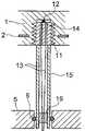
- FIG. 1is a sectional view in outline illustrating a specific example of semiconductor manufacturing equipment utilizing a common ceramic susceptor
- FIG. 2is a sectional view in outline illustrating one specific example of a temperature gauge according to the present invention
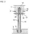
- FIG. 3is a sectional view in outline illustrating a separate specific example of a temperature gauge according to the present invention.
- FIG. 4is an oblique view in outline illustrating one specific example of a retaining member utilized in a temperature gauge of the present invention.
- FIGS. 5A and 5Bare plan views in outline illustrating respectively one end face and the other end face of the retaining member represented in FIG. 4 .
- FIG. 1An example of a semiconductor manufacturing tool equipped with a ceramic susceptor in a principal utilization of a temperature gauge is illustrated in FIG. 1 .
- the ceramic susceptor 1which is formed of a ceramic having a high thermal conductivity such as aluminum nitride, has embedded within it a resistive heating element 2 , and is provided with a thermocouple 3 for controlling its temperature.
- the ceramic susceptor 1is set up in place within a reaction chamber 5 by means of support members 4 , and lead wires 7 for supplying electricity to the resistive heating element 2 , and a lead 8 from the thermocouple 3 are accommodated within tubular members 6 . Gaps between the bottom portions of the tubular members 6 and the reaction chamber 5 are sealed gastight with O-rings 9 , and also in the bottom portion of the reaction chamber 5 water-cooling devices 10 are furthermore provided.
- the ceramic susceptor in such semiconductor manufacturing toolsis made the gauging subject, and a temperature-gauging contact in the tip of the thermocouple contacts, in an exposed-as-it-is state, and by being mechanically pressed upon is retained against, a temperature-gauging site on the gauging subject.
- thermocouple tipAs a result of concerted investigations regarding the time for the temperature being measured with a thermocouple to stabilize, the present inventors learned that with temperature gauges in conventional ceramic susceptors, due to the intervention of, surrounding the temperature-gauging contact in the thermocouple tip, the sheath, the embedded matter consisting of metal or ceramic, or the insulating material or filler material consisting of a heat-resistant resin or ceramic, heat from the temperature-gauging site is not readily transmitted to the temperature-gauging contact on account of these intervening objects, and it takes time until the measurement temperature is steady.
- thermocouple-tip temperature-gauging contactin cases where the thermocouple-tip temperature-gauging contact is directly inserted into the gauging subject, due to reaction gas invading the space, the heat capacity grows larger by that of the reaction gas, and consequently, owing to effects multiplied with those of the intervening objects just mentioned, responsiveness when gauging temperature worsens further.
- thermocouple tipis left exposed as it is, without being covered by a sheath or the like; (2) the temperature-gauging contact is directly contacted on the temperature-gauging site in the gauging subject; and (3) the temperature-gauging contact is fixed by being pressed onto the gauging subject mechanically.
- thermocouple temperature-gauging contactdirectly contacting the temperature-gauging site in an exposed as-it-is state, intervening objects such as a sheath or embedded matter, or else an insulating material or filler, are not present between means that heat from the temperature-gauging site in a ceramic susceptor or like gauging subject is readily transmitted to the temperature-gauging contact, curtailing, over what has conventionally been the case, the time until the measurement temperature stabilizes and heightening the responsiveness.
- spaceis present surrounding the temperature-gauging contact, because heat from the temperature-gauging site is transmitted directly to the temperature-gauging contact, no depreciation in responsiveness is incurred.
- thermocoupleinasmuch as the thermocouple is detachably retained against the gauging subject even in cases where the thermocouple undergoes impact on the device itself, or thermal shock when wafers are heated, and is damaged it can be easily replaced by removing the damaged thermocouple alone.
- the gauging subjectsuch as a ceramic susceptor, may therefore be reused as such, which enables the costs attendant on replacement to be kept significantly under control.
- thermocouple tipis clamped in between one end face of the retaining member 11 and the bottom face of the female screw in the ceramic susceptor 1 , and is pressed onto the ceramic susceptor 1 .
- a through-hole 14is provided in the retaining member 11 , penetrating it from one end face to the other end face, enabling lead lines 13 that go along with the temperature-gauging contact 12 in the thermocouple tip to pass through the through-hole 14 and lead out of the other end face.
- a tubular member 15is joined to the other end face of the retaining member 11 , enabling the lead lines 13 from the thermocouple to be accommodated within the tubular member 15 .
- tubular member 15a separate component of a material that is the same as or different from that of the retaining member 11 may, as depicted in the figure, be joined to the retaining member 11 using glass or a brazing material, and also can be formed unitarily with the retaining member 11 using an identical substance.
- the retaining member 16has the through-hole 14 for passing the lead lines 13 , and that the tubular member 15 may be joined to or furnished unitarily with the distal-end face of the retaining member 16 are likewise as in the FIG. 2 case.
- a columnar retaining member 16is exemplified in FIG. 3 , utilizing a plate-shaped retaining member to press the temperature-gauging contact onto the face of the ceramic susceptor on the side opposite the wafer-heating face is also possible.
- the reaction chamber insidemust be made an ambient distinct from the atmospheric ambient of the exterior. For that reason, when utilizing the temperature gauge of the present invention, in situations where as shown in FIGS. 2 and 3 the thermocouple lead lines 13 are accommodated within the tubular member 15 , the inter-space between the tubular member 15 along its distal end, and the reaction chamber 5 is sealed gastight with the O-ring 9 . Meanwhile, in cases where such a tubular member is not employed, the interspace between the thermocouple lead lines along their distal ends and the reaction chamber should be sealed gastight with a heat-resistant resin or the like.
- thermocouple lead lines 13are accommodated in the tubular member 15 the lead lines 13 along their distal ends in the interior of the tubular member 15 should be sealed gastight with sealing stuff 19 of a heat-resistant resin or the like.
- the distal-end face of the retaining member 16can, including the through-hole 14 , be sealed gastight by means of sealing stuff 20 whose thermal expansion coefficient is the same as, or approximately that of, the lead lines 13 . It should be understood that applying the gastight seal made by the sealing stuff 20 in FIG. 3 also to cases where no tubular member is utilized is possible.
- FIGS. 2 and 3are specific examples, the form of and fastening means for the retaining member, as well as the tubular member presence/absence, and the gastight sealing method are of course freely combinable.
- FIGS. 4 and 5Preferred specific examples of retaining members utilized in the present invention for the temperature-gauging contact will be explained according to FIGS. 4 and 5 .
- a retaining member 21 as depicted in FIG. 4has male threads 22 in its lateral surface, and penetrating from the proximal-end face to the distal-end face thereof two through-holes 23 for passing the thermocouple lead lines are provided.
- a recess 24is provided in the proximal-end face of the retaining member 21 so as to contain the two through-holes 23 , wherein the thermocouple temperature-gauging contact, and the lead lines that go along with it, can be housed in the recess 24 .
- FIG. 4As illustrated in FIG.
- a groove portion 25 for being turned by a screwdriver or the like when the retaining member 21 is screwed into placecan be provided in the center of its distal-end face, in between the two through-holes 23 penetrating from the proximal-end face thereof.
- the recess 24 provided in the proximal-end face of the retaining member 21 in depthbe less than the diameter of the thermocouple lead lines. Making the depth of the recess 24 less than the diameter of the lead lines, enables the temperature-gauging contact in the thermocouple to be pressed surely against the temperature-gauging site in the ceramic susceptor when attaching the retaining member 21 to the ceramic susceptor by such means as screw-joining with a female screw therein.
- the thermocouple lead lines where in between the retaining member and the bottom portion of the reaction chamberbe put into thermally resistant coverings or protective tubes with a through hole, so that the lead lines do not come into contact with each other.
- the thermal expansion coefficient of the retaining-member substancedesirably is about equal to the thermal expansion coefficient of the substance constituting the ceramic susceptor that is the gauging subject. Minimizing the difference in thermal expansion coefficient between the retaining member and the ceramic susceptor makes it possible to deter incidents of cracking in the screw joint during heating due to difference in thermal expansion coefficient.
- thermocouplemodels K, R, B, S, E, J and T as given by JIS (Japanese Industrial Standard) C 1602 (1980) are available, and application may be with any of these thermocouples.
- thermocouple alonecan easily be replaced, even in cases where the thermocouple has been damaged, by undoing the retaining member from the ceramic susceptor is advantageous in terms of efficiency and economy.
- yttriaY 2 O 3
- AlNaluminum nitride
- the obtained granulated powderwas molded by means of a uniaxial press into 2 disk forms whose post-sintering dimensions were 350 mm diameter ⁇ 10 mm thickness.
- the 2 disk-shaped molded objectswere degreased within a nitrogen atmosphere 900° C. in temperature and furthermore sintered 5 hours at a temperature of 1900° C. within a nitrogen atmosphere.
- the thermal conductivity of the AlN sinters producedwas 170 W/mK.
- the entire surface of the AlN sinterswas polished using a diamond abrasive.
- a slurry in which a sintering additive and an ethyl-cellulose binder were added into and knead-mixed with tungsten powderwas used to print a resistive-heating-element circuit superficially onto one of the disk-shaped AlN sinters, which after degreasing within a 900° C. nitrogen atmosphere were baked by being heated 1 hour at 1850° C.
- Tungsten electrode terminals connected to the resistive heating elementwere bonded to the side (reverse face) of the ceramic susceptors opposite the heating face, and furthermore electric power-supplying lead wires electrically connected to a system-external power source were connected to the electrode terminals.
- the electrode terminals and the lead wireswere accommodated in the interior of a tubular member made from a mullite sinter having a thermal conductivity of 1 W/mK, and then a B—Si bonding glass was spread onto one end face of the tubular member, which was put onto the reverse face of the ceramic susceptor, and while put under a displacement-prevention load of 50 g/cm 2 they were bonded together by being heated 1 hour at 800° C.
- a through-hole for lead lineswas provided longitudinally penetrating the round-columnar AlN sinter, and on the lateral surface thereof a male-threading process was carried out, thereby rendering a retaining member made of AlN. Furthermore a recess into which a communicating through-hole opens was machined into one end face of the retaining member. Afterwards a tubular member made from a mullite sinter, 10 mm outside diameter ⁇ 8 mm inside diameter ⁇ 100 mm length, was joined to the other end face of the retaining member using a B—Si glass.
- thermocouple insertion hole8 mm diameter ⁇ 10 mm depth, having female threads was bored into the face on the reverse of the heating face of the foregoing ceramic susceptor.
- heat-resistant coated lead wires for a K-type thermocouplewere passed through the through-hole in the retaining member just described, and a temperature-gauging contact was set onto the distal-end face of the retaining member.
- the temperature-gauging contactwas pressed by the retaining member onto the ceramic susceptor by inserting the retaining member heading from its distal-end face into thermocouple insertion hole in the ceramic susceptor and screwing the two together.
- thermocouple lead lines along their distal end and the tubular member interiorwas immobilized with a heat-resistant resin in order to form a gastight seal between the interior of the tubular member joined to the distal end of retaining member, and the exterior of reaction chamber.
- approximately circular tube-shaped support membersmade from a mullite sinter 10 mm outside diameter ⁇ 8 mm inside diameter ⁇ 100 mm length and provided with a flange on either end were fabricated the flanges along the distal ends of this plurality of approximately circular tube-shaped support members were fixed to the bottom face of the reaction chamber, and a ceramic susceptor fabricated as described above was set in place atop, without being joined to, the flanges along the proximal ends.
- the tubular members joined to the reverse face of the ceramic susceptor and the distal-end face of the retaining memberwere all sealed gastight along their respective distal ends by means of O-rings in between them and the bottom face of the reaction chamber.
- a K-type thermocouple as noted in the followingwas attached to a ceramic susceptor like that in the foregoing. Namely, prepared were: Sample 2, in which a temperature-gauging contact on a K-type thermocouple with a sheath made of SUS steel attached was inserted into a thermocouple insertion hole in a ceramic susceptor; Sample 3, in which a temperature-gauging contact on a K-type thermocouple with a sheath made of SUS steel attached was bonded with glass into a thermocouple insertion hole; and Sample 4, in which a temperature-gauging contact on a K-type thermocouple (no sheath) was inserted and embedded with glass into a thermocouple insertion hole.
- Measurement tempstabilizing stabilizing time (average) time (average) Sample During gas introduction During gas discharge 1 2 sec. 2 sec. 2* 32 sec. 21 sec. 3* 11 sec. 9 sec. 4* 3 sec. 2 sec. Note: Samples marked with an asterisk (*) in the table are comparative examples.
- a temperature gaugemay be realized in which because the thermocouple is detachable, easy replacement of the thermocouple even if damaged is possible, and meanwhile in which, with heat from the temperature-gauging site on a gauging subject being readily transmitted to the temperature-gauging contact, time until the measurement temperature stabilizes is short. Accordingly, utilizing a temperature gauge of the present invention, ceramic susceptors and semiconductor manufacturing equipment in which the ceramic susceptors are utilized may be realized wherein thermocouple replacement is facilitated, and wherein with output from the resistive heating element being controlled by temperature being gauged in a brief interval, the ceramic susceptors can be maintained at a precise temperature while their isothermal quality is preserved.
Landscapes
- Physics & Mathematics (AREA)
- General Physics & Mathematics (AREA)
- Measuring Temperature Or Quantity Of Heat (AREA)
- Control Of Resistance Heating (AREA)
- Container, Conveyance, Adherence, Positioning, Of Wafer (AREA)
- Chemical Vapour Deposition (AREA)
- Resistance Heating (AREA)
Abstract
Description
1. Field of the Invention
The present invention relates to temperature gauges for ceramic susceptors that are installed in semiconductor manufacturing equipment, and to ceramic susceptors, as well as semiconductor manufacturing equipment, utilizing the temperature gauges.
2. Description of the Background Art
Ceramic susceptors (also called wafer holders) formed from an inorganic insulating material such as a ceramic of high thermal conductivity, and in which a resistive heating element is embedded, have been employed to date in semiconductor manufacturing equipment such as CVD devices and plasma CVD devices, for example, for uniformly heating wafers on which film-forming or like processes are carried out.
In order to control the heating temperature by varying the amount of voltage and current applied to the resistive heating element, a plurality of terminals connected to the resistive heating element is furnished exposed on a face of the susceptor apart from its wafer-heating face, and the terminals and an external power source are connected by lead lines. Likewise, in order to control the temperature of the ceramic susceptor itself, a thermoelectrically matched temperature measuring component is furnished exposed on a face apart from the wafer-heating face.
With the enlarging in diametric span of wafers lately, severe demands are being placed on the temperature-control regimen for the wafer-heating face of ceramic susceptors in order to improve product yields in semiconductor manufacturing equipment. Consequently, uniformly and precisely controlling the temperature of the wafer-heating face is necessary, and temperature-measuring accuracy in the temperature-measuring components that control the output from the resistive heating element has become crucial.
Nevertheless, in measuring temperature within the reaction chambers in semiconductor manufacturing equipment, accurate temperature measurement has been difficult because the behavior of gas molecules in the temperature-measuring component environs is altered on account of pressure fluctuations stemming from the introduction and discharge of reaction gases, drastically changing how the molecules move thermally. Moreover, in cases in which the location where the temperature-measuring components are installed is remote from the wafer-heating face, the measurement temperature departing from the actual wafer temperature leads to a pronounced temperature gradient, which consequently has, depending on the case, invited circumstances in which the wafer is damaged by thermal stress.
In Japanese Pat. Pub. No. 2,644,660, for example, this is dealt with by providing a sheath in which a thermocouple is fixed and male threads on the tip portion of the sheath, which is made of metal, and by providing female threads in the ceramic susceptor, in a face of apart from its wafer-heating face, or in matter consisting of metal, ceramic, etc. embedded therein, with the male threads furnished on the tip portion for the thermocouple being screwed together with and fixed into the female threads. This enlarges the surface area in which the thermocouple and the ceramic susceptor are in direct contact, and at the same time because they are fixed by being screwed together their state of contact is unlikely to change, whereby the temperature measuring accuracy can be improved. Furthermore, the thermocouple itself is detachable/replaceable.
In other ceramic susceptor examples, proposed in Japanese Pat. App. Pub. No. 2001-244049, Japanese Pat. App. Pub. No. 2001-85143, and Japanese Pat. App. Pub. No. 2001-85144, departure between measurement temperature and wafer temperature is prevented by establishing bottomed holes, directed from the side opposite the wafer-heating face to the heating face and into which a thermocouple is inserted, and making the bottoms of the bottomed holes relatively nearer the wafer-heating face than the heating element. In addition the thermocouples are resin-sealed inside the bottomed holes after being joined into them with a brazing material, or are fixed inside the bottomed holes by filling them in with an insulating material such as a heat-resistant resin or a ceramic.
In a further ceramic susceptor example, Japanese Pat. App. Pub. No. 2002-164291, a recess whose aperture surface area is 1.0 to 30 mm2, whose depth d is, with respect to the thickness t of the heater, t/4≦d≦3t/4 is formed in the face on the side opposite the surface-heating side, and a thermocouple whose filament diameter is 0.05 to 1.0 mm and the tip portion of which is equipped with a temperature-gauging contact is inserted and adhesively fixed by means of a filler into the recess. That the temperature-measuring responsiveness is thereby improved, reducing transient temperature irregularities when heating a wafer and shortening the time until the temperature stabilizes is therein proposed.
A drawback with the ceramic susceptors set forth in the publications discussed above has been that with heat from the temperature-gauging site on the ceramic susceptor not being readily transmitted to the temperature-gauging contact, owing to the presence, surrounding the temperature-gauging contact that is on the tip of the thermocouple, of the sheath, the embedded matter consisting of metal or ceramic, or the insulating material or filler material consisting of a heat-resistant resin or ceramic, it takes time for the measurement temperature to stabilize.
Another problem has been that the temperature-measuring element generally employed in thermocouples is thin-gauge because it must be confined within limited space, and consequently the temperature-measuring element, undergoing impact on the device itself or thermal shock when wafers are heated, is in some cases damaged. With the ceramic susceptors set forth in the disclosures in Japanese Pat. App. Pub. No. 2001-244049, Pat. App. Pub. No. 2001-85143, Pat. App. Pub. No. 2001-85144, and Pat. App. Pub. No. 2002-164291, in particular, because the temperature-measuring element is fixed by being joined or embedded in place, replacing the entire ceramic susceptor is necessary if the temperature-measuring element has been damaged, which has made the replacement work a large-scale undertaking, and on top of that the costs attendant on replacement have been great.
An object of the present invention, in view of such circumstances to date, is to render a temperature gauge in which simple replacement of the thermocouple even if damaged is possible, and moreover in which heat from the temperature-gauging site is readily transmitted to the temperature-gauging contact, shortening time until the measurement temperature stabilizes. In addition, the present invention realizes ceramic susceptors and semiconductor manufacturing equipment utilizing a temperature gauge of this sort.
In order to achieve the foregoing objective, a temperature gauge that the present invention realizes is characterized in that a temperature-gauging contact in the tip of the thermocouple contacts in an exposed-as-it-is state, and by being mechanically, detachably pressed upon is retained against, the temperature-gauging site on an article subjected to temperature gauging.
The foregoing temperature gauge by the present invention preferably is characterized in that the temperature-gauging contact in the thermocouple tip is clamped in between a retaining member and a gauging subject that screw into, or are screwlocked to, each other.
The foregoing temperature gauge by the present invention is in specific aspects characterized in that the aforementioned retaining member is a circular cylindrical form having male threads in its lateral surface, and by means of the male threads is screwed together with female threads provided in the gauging subject, whereby with one end face of the retaining member the temperature-gauging contact is pressed onto the gauging subject; or else is characterized in that the retaining member has, along one end thereof, a flange portion provided with threaded holes and that is screwlocked into female screws provided in a surface of the gauging subject.
In the foregoing temperature gauge by the present invention, the retaining member has a through-hole penetrating from one end face to the other end face thereof, wherein lead lines from the thermocouple can be passed into the through-hole. Alternatively, the retaining member is in an end face thereof furnished with a recess into which a communicating through-hole opens, wherein the temperature-gauging contact in the thermocouple tip and the lead lines that go along with it can be housed in the recess. Moreover, the depth of the recess preferably is less than the diameter of the thermocouple lead lines.
Also preferable in the foregoing temperature gauge by the present invention is that a tubular member for accommodating the thermocouple lead lines is either joined to or is furnished integrally with the other end face of the retaining member. In addition, either the other end face of the retaining member, or along its distal end the tubular member, joined to or otherwise furnished integrally with the retaining member, is preferably sealed gastight by means of a sealing member. Still further, the thermal expansion coefficient of the retaining member preferably is about equal to the thermal expansion coefficient of the gauging subject.
The present invention likewise renders ceramic susceptors characterized in being furnished with an above-described temperature-gauging device by the present invention. Furthermore, the present invention realizes semiconductor manufacturing equipment characterized in being fitted out with such ceramic susceptors.
From the following detailed description in conjunction with the accompanying drawings, the foregoing and other objects, features, aspects and advantages of the present invention will become readily apparent to those skilled in the art.
An example of a semiconductor manufacturing tool equipped with a ceramic susceptor in a principal utilization of a temperature gauge is illustrated inFIG. 1 . Theceramic susceptor 1, which is formed of a ceramic having a high thermal conductivity such as aluminum nitride, has embedded within it aresistive heating element 2, and is provided with a thermocouple3 for controlling its temperature. Theceramic susceptor 1 is set up in place within areaction chamber 5 by means ofsupport members 4, and leadwires 7 for supplying electricity to theresistive heating element 2, and alead 8 from the thermocouple3 are accommodated withintubular members 6. Gaps between the bottom portions of thetubular members 6 and thereaction chamber 5 are sealed gastight with O-rings 9, and also in the bottom portion of thereaction chamber 5 water-coolingdevices 10 are furthermore provided.
With a temperature gauge in the present invention, the ceramic susceptor in such semiconductor manufacturing tools is made the gauging subject, and a temperature-gauging contact in the tip of the thermocouple contacts, in an exposed-as-it-is state, and by being mechanically pressed upon is retained against, a temperature-gauging site on the gauging subject.
As a result of concerted investigations regarding the time for the temperature being measured with a thermocouple to stabilize, the present inventors learned that with temperature gauges in conventional ceramic susceptors, due to the intervention of, surrounding the temperature-gauging contact in the thermocouple tip, the sheath, the embedded matter consisting of metal or ceramic, or the insulating material or filler material consisting of a heat-resistant resin or ceramic, heat from the temperature-gauging site is not readily transmitted to the temperature-gauging contact on account of these intervening objects, and it takes time until the measurement temperature is steady.
They also learned that if space is present surrounding the temperature-gauging contact in the thermocouple tip, as in cases where the thermocouple-tip temperature-gauging contact is directly inserted into the gauging subject, due to reaction gas invading the space, the heat capacity grows larger by that of the reaction gas, and consequently, owing to effects multiplied with those of the intervening objects just mentioned, responsiveness when gauging temperature worsens further.
To address these issues, three means have been adopted in the present invention in order to heighten the responsiveness: (1) the temperature-gauging contact in the thermocouple tip is left exposed as it is, without being covered by a sheath or the like; (2) the temperature-gauging contact is directly contacted on the temperature-gauging site in the gauging subject; and (3) the temperature-gauging contact is fixed by being pressed onto the gauging subject mechanically.
By adopting this configuration, in a temperature gauge of the present invention, the fact that with the thermocouple temperature-gauging contact directly contacting the temperature-gauging site in an exposed as-it-is state, intervening objects such as a sheath or embedded matter, or else an insulating material or filler, are not present between means that heat from the temperature-gauging site in a ceramic susceptor or like gauging subject is readily transmitted to the temperature-gauging contact, curtailing, over what has conventionally been the case, the time until the measurement temperature stabilizes and heightening the responsiveness. Meanwhile, although space is present surrounding the temperature-gauging contact, because heat from the temperature-gauging site is transmitted directly to the temperature-gauging contact, no depreciation in responsiveness is incurred.
What is more, with a temperature gauge of the present invention, inasmuch as the thermocouple is detachably retained against the gauging subject even in cases where the thermocouple undergoes impact on the device itself, or thermal shock when wafers are heated, and is damaged it can be easily replaced by removing the damaged thermocouple alone. The gauging subject, such as a ceramic susceptor, may therefore be reused as such, which enables the costs attendant on replacement to be kept significantly under control.
As means in the present invention for detachably retaining the thermocouple in an exposed as-it-is state against the gauging subject, it is preferable to utilize a retaining member to press the temperature-gauging contact in the thermocouple tip onto, and clamp it together with, the gauging subject, and either to screw the retaining member and the gauging subject together by mutually threaded portions in each, or to provide threaded holes in each and screwlock them.
Next, a temperature gauge by the present invention will be specifically explained with reference to the drawings. It should be understood that components that are the same as those of the example illustrated inFIG. 1 are labeled with identical reference mark, and explanation thereof is omitted.
To begin with, in the temperature gauge illustrated inFIG. 2 , employing a retainingmember 11 of circular cylindrical form having male threads in its lateral surface and screwing the male threads into a female screw provided in the face of theceramic susceptor 1 on the side opposite its wafer-heating face, makes it so that the temperature-gaugingcontact 12 in the thermocouple tip is clamped in between one end face of the retainingmember 11 and the bottom face of the female screw in theceramic susceptor 1, and is pressed onto theceramic susceptor 1.
A through-hole 14 is provided in the retainingmember 11, penetrating it from one end face to the other end face, enablinglead lines 13 that go along with the temperature-gaugingcontact 12 in the thermocouple tip to pass through the through-hole 14 and lead out of the other end face. In turn, atubular member 15 is joined to the other end face of the retainingmember 11, enabling the lead lines13 from the thermocouple to be accommodated within thetubular member 15. It will be appreciated that for thetubular member 15, a separate component of a material that is the same as or different from that of the retainingmember 11 may, as depicted in the figure, be joined to the retainingmember 11 using glass or a brazing material, and also can be formed unitarily with the retainingmember 11 using an identical substance.
Alternatively, in the temperature gauge illustrated inFIG. 3 aflange 17 having threaded holes is provided along the distal end of acolumnar retaining member 16, and the retainingmember 16 is inserted into an insertion hole provided in the face of theceramic susceptor 1 on the side opposite its wafer-heating side, whereinmale screws 18 are screwed into and screwlock the threaded holes in theflange 17 and female screws furnished in theceramic susceptor 1. The temperature-gaugingcontact 12 in the thermocouple tip is thereby clamped in between the proximal-end face of the retainingmember 16 and the bottom face of the insertion hole in theceramic susceptor 1, and pressed onto theceramic susceptor 1.
Here, in the specific example ofFIG. 3 as well, that the retainingmember 16 has the through-hole 14 for passing the lead lines13, and that thetubular member 15 may be joined to or furnished unitarily with the distal-end face of the retainingmember 16 are likewise as in theFIG. 2 case. It should also be understood that although acolumnar retaining member 16 is exemplified inFIG. 3 , utilizing a plate-shaped retaining member to press the temperature-gauging contact onto the face of the ceramic susceptor on the side opposite the wafer-heating face is also possible.
It will be appreciated that in a semiconductor manufacturing tool, the reaction chamber inside must be made an ambient distinct from the atmospheric ambient of the exterior. For that reason, when utilizing the temperature gauge of the present invention, in situations where as shown inFIGS. 2 and 3 thethermocouple lead lines 13 are accommodated within thetubular member 15, the inter-space between thetubular member 15 along its distal end, and thereaction chamber 5 is sealed gastight with the O-ring 9. Meanwhile, in cases where such a tubular member is not employed, the interspace between the thermocouple lead lines along their distal ends and the reaction chamber should be sealed gastight with a heat-resistant resin or the like.
On the other hand, because in the present invention there is a through-hole in the retaining member for the thermocouple lead lines passing the through hole, the interior of the tubular member ends up being the atmospheric ambient external to the reaction chamber. That is because a gastight condition within the reaction chamber cannot be maintained the interior of the tubular member must also be made gastight with respect to the reaction chamber exterior. In that regard, in cases where, as shown inFIG. 2 for example, thethermocouple lead lines 13 are accommodated in thetubular member 15 the lead lines13 along their distal ends in the interior of thetubular member 15 should be sealed gastight with sealingstuff 19 of a heat-resistant resin or the like.
By the same token, as shown inFIG. 3 , the distal-end face of the retainingmember 16 can, including the through-hole 14, be sealed gastight by means of sealingstuff 20 whose thermal expansion coefficient is the same as, or approximately that of, the lead lines13. It should be understood that applying the gastight seal made by the sealingstuff 20 inFIG. 3 also to cases where no tubular member is utilized is possible. Here, whileFIGS. 2 and 3 are specific examples, the form of and fastening means for the retaining member, as well as the tubular member presence/absence, and the gastight sealing method are of course freely combinable.
Preferred specific examples of retaining members utilized in the present invention for the temperature-gauging contact will be explained according toFIGS. 4 and 5 . Here a retainingmember 21 as depicted inFIG. 4 hasmale threads 22 in its lateral surface, and penetrating from the proximal-end face to the distal-end face thereof two through-holes 23 for passing the thermocouple lead lines are provided. In addition, as shown inFIG. 4 andFIG. 5A , arecess 24 is provided in the proximal-end face of the retainingmember 21 so as to contain the two through-holes 23, wherein the thermocouple temperature-gauging contact, and the lead lines that go along with it, can be housed in therecess 24. Moreover, as illustrated inFIG. 5B agroove portion 25 for being turned by a screwdriver or the like when the retainingmember 21 is screwed into place can be provided in the center of its distal-end face, in between the two through-holes 23 penetrating from the proximal-end face thereof.
It is desirable that therecess 24 provided in the proximal-end face of the retainingmember 21 in depth be less than the diameter of the thermocouple lead lines. Making the depth of therecess 24 less than the diameter of the lead lines, enables the temperature-gauging contact in the thermocouple to be pressed surely against the temperature-gauging site in the ceramic susceptor when attaching the retainingmember 21 to the ceramic susceptor by such means as screw-joining with a female screw therein. Likewise, it is desirable that the thermocouple lead lines where in between the retaining member and the bottom portion of the reaction chamber be put into thermally resistant coverings or protective tubes with a through hole, so that the lead lines do not come into contact with each other.
The thermal expansion coefficient of the retaining-member substance desirably is about equal to the thermal expansion coefficient of the substance constituting the ceramic susceptor that is the gauging subject. Minimizing the difference in thermal expansion coefficient between the retaining member and the ceramic susceptor makes it possible to deter incidents of cracking in the screw joint during heating due to difference in thermal expansion coefficient.
Here, as far as the thermocouple is concerned models K, R, B, S, E, J and T as given by JIS (Japanese Industrial Standard) C 1602 (1980) are available, and application may be with any of these thermocouples.
In a ceramic susceptor utilizing a temperature gauge of the present invention, output from the resistive heating element is controlled by gauging the susceptor temperature in a brief interval, enabling the susceptor to be maintained at a precise temperature while preserving the isothermal quality of its heating face. What is more, the fact that the thermocouple alone can easily be replaced, even in cases where the thermocouple has been damaged, by undoing the retaining member from the ceramic susceptor is advantageous in terms of efficiency and economy.
0.5 parts by weight yttria (Y2O3) as a sintering additive was added to 100 parts by weight aluminum nitride (AlN) powder, and was further combined with a predetermined amount of an organic extrusion binder; and after mixing these ingredients using a ball-mixing method the blend was granulated by spray-drying. The obtained granulated powder was molded by means of a uniaxial press into 2 disk forms whose post-sintering dimensions were 350 mm diameter×10 mm thickness. The 2 disk-shaped molded objects were degreased within a nitrogen atmosphere 900° C. in temperature and furthermore sintered 5 hours at a temperature of 1900° C. within a nitrogen atmosphere. The thermal conductivity of the AlN sinters produced was 170 W/mK. The entire surface of the AlN sinters was polished using a diamond abrasive.
A slurry in which a sintering additive and an ethyl-cellulose binder were added into and knead-mixed with tungsten powder was used to print a resistive-heating-element circuit superficially onto one of the disk-shaped AlN sinters, which after degreasing within a 900° C. nitrogen atmosphere were baked by being heated 1 hour at 1850° C. A slurry in which an ethyl-cellulose binder was added to and knead-mixed with a bonding glass was spread onto the other disk-shaped AlN sinter, which was degreased within a 900° C. nitrogen atmosphere. The bonding-glass face and the resistive-heating-element face of the two AlN sinter plies were stacked together, and while put under a displacement-prevention load of 5 kg/cm2were bonded together being heated 2 hours at 1800° C., whereby ceramic susceptors interiorly in which a resistive heating element was embedded were fabricated.
Tungsten electrode terminals connected to the resistive heating element were bonded to the side (reverse face) of the ceramic susceptors opposite the heating face, and furthermore electric power-supplying lead wires electrically connected to a system-external power source were connected to the electrode terminals. The electrode terminals and the lead wires were accommodated in the interior of a tubular member made from a mullite sinter having a thermal conductivity of 1 W/mK, and then a B—Si bonding glass was spread onto one end face of the tubular member, which was put onto the reverse face of the ceramic susceptor, and while put under a displacement-prevention load of 50 g/cm2they were bonded together by being heated 1 hour at 800° C.
In addition, after knead-mixing a blend utilizing the same AlN powder as that used when the AlN sinters described above were manufactured, with the sintering additive composition being the same, and further combined with an organic extrusion binder, a dispersing agent, and a solvent, a round columnar form whose post-sintering dimensions were 10 mm outside diameter×8 mm length was molded by extrusion molding the blend. The round-columnar molded object was degreased and sintered under the same conditions as during the manufacture of the foregoing AlN sinters, whereby ALN sinters whose the thermal conductivity was 170 W/mK were obtained. A through-hole for lead lines was provided longitudinally penetrating the round-columnar AlN sinter, and on the lateral surface thereof a male-threading process was carried out, thereby rendering a retaining member made of AlN. Furthermore a recess into which a communicating through-hole opens was machined into one end face of the retaining member. Afterwards a tubular member made from a mullite sinter, 10 mm outside diameter×8 mm inside diameter×100 mm length, was joined to the other end face of the retaining member using a B—Si glass.
In turn, a thermocouple insertion hole, 8 mm diameter×10 mm depth, having female threads was bored into the face on the reverse of the heating face of the foregoing ceramic susceptor. Meanwhile, heat-resistant coated lead wires for a K-type thermocouple were passed through the through-hole in the retaining member just described, and a temperature-gauging contact was set onto the distal-end face of the retaining member. The temperature-gauging contact was pressed by the retaining member onto the ceramic susceptor by inserting the retaining member heading from its distal-end face into thermocouple insertion hole in the ceramic susceptor and screwing the two together. After that, the interspace between the thermocouple lead lines along their distal end and the tubular member interior, was immobilized with a heat-resistant resin in order to form a gastight seal between the interior of the tubular member joined to the distal end of retaining member, and the exterior of reaction chamber.
In addition, approximately circular tube-shaped support members, made from amullite sinter 10 mm outside diameter×8 mm inside diameter×100 mm length and provided with a flange on either end were fabricated the flanges along the distal ends of this plurality of approximately circular tube-shaped support members were fixed to the bottom face of the reaction chamber, and a ceramic susceptor fabricated as described above was set in place atop, without being joined to, the flanges along the proximal ends. The tubular members joined to the reverse face of the ceramic susceptor and the distal-end face of the retaining member were all sealed gastight along their respective distal ends by means of O-rings in between them and the bottom face of the reaction chamber.
In respect of aceramic susceptor Sample 1 to which a temperature gauge according to the present invention example, fabricated as stated above, its reaction chamber interior was drawn down to a vacuum (10−2Pa or less) and the ceramic susceptor was heated to a temperature of 500° C. An operation of in that sate introducing N2gas into the chamber until the internal pressure was 1 atmosphere and once more discharging the chamber down to a vacuum was repeated for 10 cycles, and respectively during introduction and during discharge of the gas the time (average) until the case-monitor temperatures stabilized was measured. It should be understood that in making these measurements, a disk-shaped block made from a substance having a large heat capacity was set onto the wafer-heating face of the ceramic susceptor in order to eliminate variation in the temperature of the susceptor itself.
For comparison, a K-type thermocouple as noted in the following was attached to a ceramic susceptor like that in the foregoing. Namely, prepared were:Sample 2, in which a temperature-gauging contact on a K-type thermocouple with a sheath made of SUS steel attached was inserted into a thermocouple insertion hole in a ceramic susceptor; Sample 3, in which a temperature-gauging contact on a K-type thermocouple with a sheath made of SUS steel attached was bonded with glass into a thermocouple insertion hole; andSample 4, in which a temperature-gauging contact on a K-type thermocouple (no sheath) was inserted and embedded with glass into a thermocouple insertion hole.
With regard to theseSamples 2 through 4 also, the time (average) until the measurement temperature stabilized was found in the same manner as with the foregoingSample 1, and the results are set forth, together with those forSample 1, in the table below. As will be understood from the table, present-invention Sample 1, in which a K-type thermocouple was pressed onto a ceramic susceptor by a retaining member screwed together there-with yielded stabilizing times about equal to those that were the case withSample 4, wherein the temperature-gauging contact was embedded with glass so as not to undergo any pressure fluctuation whatsoever within the reaction chamber.
| TABLE | ||
| Measurement temp. | Measurement temp. | |
| stabilizing | stabilizing | |
| time (average) | time (average) | |
| Sample | During gas introduction | During |
| 1 | 2 sec. | 2 sec. |
| 2* | 32 sec. | 21 sec. |
| 3* | 11 sec. | 9 sec. |
| 4* | 3 sec. | 2 sec. |
| Note: Samples marked with an asterisk (*) in the table are comparative examples. | ||
As given by the present invention, a temperature gauge may be realized in which because the thermocouple is detachable, easy replacement of the thermocouple even if damaged is possible, and meanwhile in which, with heat from the temperature-gauging site on a gauging subject being readily transmitted to the temperature-gauging contact, time until the measurement temperature stabilizes is short. Accordingly, utilizing a temperature gauge of the present invention, ceramic susceptors and semiconductor manufacturing equipment in which the ceramic susceptors are utilized may be realized wherein thermocouple replacement is facilitated, and wherein with output from the resistive heating element being controlled by temperature being gauged in a brief interval, the ceramic susceptors can be maintained at a precise temperature while their isothermal quality is preserved.
Only selected embodiments have been chosen to illustrate the present invention. To those skilled in the art, however, it will be apparent from the foregoing disclosure that various changes and modifications can be made herein without departing from the scope of the invention as defined in the appended claims. Furthermore, the foregoing description of the embodiments according to the present invention is provided for illustration only, and not for limiting the invention as defined by the appended claims and their equivalents.
Claims (16)
1. A ceramic susceptor including a temperature gauge for gauging the temperature of a temperature-gauging site in the susceptor, the temperature gauge comprising:
a thermocouple having a tip end;
a temperature-gauging contact exposed in the tip end of said thermocouple and contacting, exposed as it is, the temperature-gauging site in the susceptor; and
a detachable retaining member that either screws together with or is screwlocked into the susceptor, for clamping said temperature-gauging contact in between said retaining member and the susceptor, thereby mechanically pressing upon said temperature-gauging contact to retain it against the temperature-gauging site, said retaining member in an end face thereof being furnished with a recess into which a communicating through-hole opens, so that said temperature-gauging contact in the thermocouple tip and lead lines accompanying said contact can be housed in the recess, and said recess in depth measuring less than the thermocouple lead lines in diameter.
2. A ceramic susceptor including a temperature gauge as set forth inclaim 1 , female screws being provided in a surface of the susceptor, wherein said retaining member has, along one end thereof, a flange portion provided with threaded holes for screwlocking said retaining member into the female screws in the susceptor.
3. A ceramic susceptor including a temperature gauge as set forth inclaim 1 , wherein the retaining member has a through-hole penetrating from one end face to the other end face thereof so that lead lines from the thermocouple can be passed into the through-hole.
4. A ceramic susceptor including a temperature gauge as set forth inclaim 1 , further comprising a tubular member, either joined to or furnished integrally with an end face of said retaining member opposite where said temperature-gauging contact is clamped, for accommodating lead lines from said thermocouple.
5. A ceramic susceptor including a temperature gauge as set forth inclaim 1 , wherein the thermal expansion coefficient of said retaining member is about equal to the thermal expansion coefficient of the susceptor.
6. A ceramic susceptor including a temperature gauge as set forth inclaim 1 , female threads being provided in the susceptor, wherin said retaining member is a circularly cylindrical form having male threads in its lateral surface for screwing said retaining member together with the female threads in the susceptor so that one end face of the retaining member presses said temperature-gauging contact onto the susceptor.
7. A ceramic susceptor including a temperature gauge as set forth inclaim 6 , wherein the other end face of said circularly cylindrical retaining member has a groove for being turned by a turning tool when said retaining member is screwed together with the susceptor.
8. Semiconductor manufacturing equipment furnished with a ceramic susceptor as recited inclaim 1 .
9. A ceramic susceptor including a temperature gauge for gauging the temperature of a temperature-gauging site in a susceptor subjected to temperature gauging, the temperature gauge comprising:
a thermocouple having a tip end;
a temperature-gauging contact exposed in the tip end of said thermocouple and contacting, exposed as it is, the temperature-gauging site in the susceptor;
a detachable retaining member that either screws together with or is screwlocked into the susceptor, for clamping said temperature-gauging contact in between said retaining member and the susceptor, thereby mechanically pressing upon said temperature-gauging contact to retain it against the temperature-gauging site; and
a sealing member for sealing gastight either an end face of said retaining member opposite where said temperature-gauging contact is clamped, or sealing distal-endwise a tubular member joined to or otherwise furnished integrally with said retaining member.
10. A ceramic susceptor including a temperature gauge as set forth inclaim 9 , female screws being provided in a surface of the susceptor, wherein said retaining member has, along one end thereof, a flange portion provided with threaded holes for screwlocking said retaining member into the female screws in the susceptor.
11. A ceramic susceptor including a temperature gauge as set forth inclaim 9 , wherein the retaining member has a through-hole penetrating from one end face to the other end face thereof so that lead lines from the thermocouple can be passed into the through-hole.
12. A ceramic susceptor including a temperature gauge as set forth inclaim 9 , further comprising a tubular member, either joined to or furnished integrally with an end face of said retaining member opposite where said temperature-gauging contact is clamped, for accommodating lead lines from said thermocouple.
13. A ceramic susceptor including a temperature gauge as set forth inclaim 9 , wherein the thermal expansion coefficient of said retaining member is about equal to the thermal expansion coefficient of the susceptor.
14. A ceramic susceptor including a temperature gauge as set forth inclaim 9 , female threads being provided in the susceptor, wherein said retaining member is a circularly cylindrical form having male threads in its lateral surface for screwing said retaining member together with the female threads in the susceptor so that one end face of the retaining member presses said temperature-gauging contact onto the susceptor.
15. A ceramic susceptor including a temperature gauge as set forth inclaim 14 , wherein the other end face of said circularly cylindrical retaining member has a groove for being turned by a turning tool when said retaining member is screwed together with the susceptor.
16. Semiconductor manufacturing equipment furnished with a ceramic susceptor as recited inclaim 9 .
Applications Claiming Priority (2)
| Application Number | Priority Date | Filing Date | Title |
|---|---|---|---|
| JP2002294399AJP3671951B2 (en) | 2002-10-08 | 2002-10-08 | Temperature measuring device and ceramic heater using the same |
| JPJP-2002-294399 | 2002-10-08 |
Publications (2)
| Publication Number | Publication Date |
|---|---|
| US20040208228A1 US20040208228A1 (en) | 2004-10-21 |
| US7090394B2true US7090394B2 (en) | 2006-08-15 |
Family
ID=32284946
Family Applications (1)
| Application Number | Title | Priority Date | Filing Date |
|---|---|---|---|
| US10/605,519Expired - Fee RelatedUS7090394B2 (en) | 2002-10-08 | 2003-10-06 | Temperature gauge and ceramic susceptor in which it is utilized |
Country Status (3)
| Country | Link |
|---|---|
| US (1) | US7090394B2 (en) |
| JP (1) | JP3671951B2 (en) |
| TW (1) | TWI333388B (en) |
Cited By (358)
| Publication number | Priority date | Publication date | Assignee | Title |
|---|---|---|---|---|
| US20070086503A1 (en)* | 2004-07-01 | 2007-04-19 | Yoshinori Fujii | Substrate temperature measurement apparatus and processing apparatus |
| US20100145547A1 (en)* | 2008-12-08 | 2010-06-10 | Asm America, Inc. | Thermocouple |
| US20100286842A1 (en)* | 2009-05-06 | 2010-11-11 | Asm America, Inc. | Smart Temperature Measuring Device |
| US20100282163A1 (en)* | 2009-05-06 | 2010-11-11 | Asm America, Inc. | Thermocouple assembly with guarded thermocouple junction |
| US20100284438A1 (en)* | 2009-05-06 | 2010-11-11 | Asm America, Inc. | Thermocouple |
| USD702188S1 (en) | 2013-03-08 | 2014-04-08 | Asm Ip Holding B.V. | Thermocouple |
| US20170211989A1 (en)* | 2016-01-21 | 2017-07-27 | Aktiebolaget Skf | Method and device for assembling a temperature sensor |
| US10229833B2 (en) | 2016-11-01 | 2019-03-12 | Asm Ip Holding B.V. | Methods for forming a transition metal nitride film on a substrate by atomic layer deposition and related semiconductor device structures |
| US10249577B2 (en) | 2016-05-17 | 2019-04-02 | Asm Ip Holding B.V. | Method of forming metal interconnection and method of fabricating semiconductor apparatus using the method |
| US10249524B2 (en) | 2017-08-09 | 2019-04-02 | Asm Ip Holding B.V. | Cassette holder assembly for a substrate cassette and holding member for use in such assembly |
| US10262859B2 (en) | 2016-03-24 | 2019-04-16 | Asm Ip Holding B.V. | Process for forming a film on a substrate using multi-port injection assemblies |
| US10269558B2 (en) | 2016-12-22 | 2019-04-23 | Asm Ip Holding B.V. | Method of forming a structure on a substrate |
| US10276355B2 (en) | 2015-03-12 | 2019-04-30 | Asm Ip Holding B.V. | Multi-zone reactor, system including the reactor, and method of using the same |
| US10283353B2 (en) | 2017-03-29 | 2019-05-07 | Asm Ip Holding B.V. | Method of reforming insulating film deposited on substrate with recess pattern |
| US10290508B1 (en) | 2017-12-05 | 2019-05-14 | Asm Ip Holding B.V. | Method for forming vertical spacers for spacer-defined patterning |
| US10312129B2 (en) | 2015-09-29 | 2019-06-04 | Asm Ip Holding B.V. | Variable adjustment for precise matching of multiple chamber cavity housings |
| US10312055B2 (en) | 2017-07-26 | 2019-06-04 | Asm Ip Holding B.V. | Method of depositing film by PEALD using negative bias |
| US10319588B2 (en) | 2017-10-10 | 2019-06-11 | Asm Ip Holding B.V. | Method for depositing a metal chalcogenide on a substrate by cyclical deposition |
| US10322384B2 (en) | 2015-11-09 | 2019-06-18 | Asm Ip Holding B.V. | Counter flow mixer for process chamber |
| US10340135B2 (en) | 2016-11-28 | 2019-07-02 | Asm Ip Holding B.V. | Method of topologically restricted plasma-enhanced cyclic deposition of silicon or metal nitride |
| US10340125B2 (en) | 2013-03-08 | 2019-07-02 | Asm Ip Holding B.V. | Pulsed remote plasma method and system |
| US10343920B2 (en) | 2016-03-18 | 2019-07-09 | Asm Ip Holding B.V. | Aligned carbon nanotubes |
| US10361201B2 (en) | 2013-09-27 | 2019-07-23 | Asm Ip Holding B.V. | Semiconductor structure and device formed using selective epitaxial process |
| US10364493B2 (en) | 2016-08-25 | 2019-07-30 | Asm Ip Holding B.V. | Exhaust apparatus and substrate processing apparatus having an exhaust line with a first ring having at least one hole on a lateral side thereof placed in the exhaust line |
| US10364496B2 (en) | 2011-06-27 | 2019-07-30 | Asm Ip Holding B.V. | Dual section module having shared and unshared mass flow controllers |
| US10367080B2 (en) | 2016-05-02 | 2019-07-30 | Asm Ip Holding B.V. | Method of forming a germanium oxynitride film |
| US10366864B2 (en) | 2013-03-08 | 2019-07-30 | Asm Ip Holding B.V. | Method and system for in-situ formation of intermediate reactive species |
| US10381219B1 (en) | 2018-10-25 | 2019-08-13 | Asm Ip Holding B.V. | Methods for forming a silicon nitride film |
| US10378106B2 (en) | 2008-11-14 | 2019-08-13 | Asm Ip Holding B.V. | Method of forming insulation film by modified PEALD |
| US10381226B2 (en) | 2016-07-27 | 2019-08-13 | Asm Ip Holding B.V. | Method of processing substrate |
| US10388513B1 (en) | 2018-07-03 | 2019-08-20 | Asm Ip Holding B.V. | Method for depositing silicon-free carbon-containing film as gap-fill layer by pulse plasma-assisted deposition |
| US10388509B2 (en) | 2016-06-28 | 2019-08-20 | Asm Ip Holding B.V. | Formation of epitaxial layers via dislocation filtering |
| US10395919B2 (en) | 2016-07-28 | 2019-08-27 | Asm Ip Holding B.V. | Method and apparatus for filling a gap |
| US10403504B2 (en) | 2017-10-05 | 2019-09-03 | Asm Ip Holding B.V. | Method for selectively depositing a metallic film on a substrate |
| US10410943B2 (en) | 2016-10-13 | 2019-09-10 | Asm Ip Holding B.V. | Method for passivating a surface of a semiconductor and related systems |
| US10438965B2 (en) | 2014-12-22 | 2019-10-08 | Asm Ip Holding B.V. | Semiconductor device and manufacturing method thereof |
| US10435790B2 (en) | 2016-11-01 | 2019-10-08 | Asm Ip Holding B.V. | Method of subatmospheric plasma-enhanced ALD using capacitively coupled electrodes with narrow gap |
| US10446393B2 (en) | 2017-05-08 | 2019-10-15 | Asm Ip Holding B.V. | Methods for forming silicon-containing epitaxial layers and related semiconductor device structures |
| US10458018B2 (en) | 2015-06-26 | 2019-10-29 | Asm Ip Holding B.V. | Structures including metal carbide material, devices including the structures, and methods of forming same |
| US10468262B2 (en) | 2017-02-15 | 2019-11-05 | Asm Ip Holding B.V. | Methods for forming a metallic film on a substrate by a cyclical deposition and related semiconductor device structures |
| US10468251B2 (en) | 2016-02-19 | 2019-11-05 | Asm Ip Holding B.V. | Method for forming spacers using silicon nitride film for spacer-defined multiple patterning |
| US10483099B1 (en) | 2018-07-26 | 2019-11-19 | Asm Ip Holding B.V. | Method for forming thermally stable organosilicon polymer film |
| US10480072B2 (en) | 2009-04-06 | 2019-11-19 | Asm Ip Holding B.V. | Semiconductor processing reactor and components thereof |
| US10504742B2 (en) | 2017-05-31 | 2019-12-10 | Asm Ip Holding B.V. | Method of atomic layer etching using hydrogen plasma |
| US10501866B2 (en) | 2016-03-09 | 2019-12-10 | Asm Ip Holding B.V. | Gas distribution apparatus for improved film uniformity in an epitaxial system |
| US10510536B2 (en) | 2018-03-29 | 2019-12-17 | Asm Ip Holding B.V. | Method of depositing a co-doped polysilicon film on a surface of a substrate within a reaction chamber |
| US10529554B2 (en) | 2016-02-19 | 2020-01-07 | Asm Ip Holding B.V. | Method for forming silicon nitride film selectively on sidewalls or flat surfaces of trenches |
| US10529563B2 (en) | 2017-03-29 | 2020-01-07 | Asm Ip Holdings B.V. | Method for forming doped metal oxide films on a substrate by cyclical deposition and related semiconductor device structures |
| US10529542B2 (en) | 2015-03-11 | 2020-01-07 | Asm Ip Holdings B.V. | Cross-flow reactor and method |
| US10535516B2 (en) | 2018-02-01 | 2020-01-14 | Asm Ip Holdings B.V. | Method for depositing a semiconductor structure on a surface of a substrate and related semiconductor structures |
| US10541333B2 (en) | 2017-07-19 | 2020-01-21 | Asm Ip Holding B.V. | Method for depositing a group IV semiconductor and related semiconductor device structures |
| US10541173B2 (en) | 2016-07-08 | 2020-01-21 | Asm Ip Holding B.V. | Selective deposition method to form air gaps |
| US10559458B1 (en) | 2018-11-26 | 2020-02-11 | Asm Ip Holding B.V. | Method of forming oxynitride film |
| US10561975B2 (en) | 2014-10-07 | 2020-02-18 | Asm Ip Holdings B.V. | Variable conductance gas distribution apparatus and method |
| US10566223B2 (en) | 2012-08-28 | 2020-02-18 | Asm Ip Holdings B.V. | Systems and methods for dynamic semiconductor process scheduling |
| US10590535B2 (en) | 2017-07-26 | 2020-03-17 | Asm Ip Holdings B.V. | Chemical treatment, deposition and/or infiltration apparatus and method for using the same |
| US10600673B2 (en) | 2015-07-07 | 2020-03-24 | Asm Ip Holding B.V. | Magnetic susceptor to baseplate seal |
| US10605530B2 (en) | 2017-07-26 | 2020-03-31 | Asm Ip Holding B.V. | Assembly of a liner and a flange for a vertical furnace as well as the liner and the vertical furnace |
| US10607895B2 (en) | 2017-09-18 | 2020-03-31 | Asm Ip Holdings B.V. | Method for forming a semiconductor device structure comprising a gate fill metal |
| US10604847B2 (en) | 2014-03-18 | 2020-03-31 | Asm Ip Holding B.V. | Gas distribution system, reactor including the system, and methods of using the same |
| US10612136B2 (en) | 2018-06-29 | 2020-04-07 | ASM IP Holding, B.V. | Temperature-controlled flange and reactor system including same |
| USD880437S1 (en) | 2018-02-01 | 2020-04-07 | Asm Ip Holding B.V. | Gas supply plate for semiconductor manufacturing apparatus |
| US10612137B2 (en) | 2016-07-08 | 2020-04-07 | Asm Ip Holdings B.V. | Organic reactants for atomic layer deposition |
| US10622375B2 (en) | 2016-11-07 | 2020-04-14 | Asm Ip Holding B.V. | Method of processing a substrate and a device manufactured by using the method |
| US10643904B2 (en) | 2016-11-01 | 2020-05-05 | Asm Ip Holdings B.V. | Methods for forming a semiconductor device and related semiconductor device structures |
| US10643826B2 (en) | 2016-10-26 | 2020-05-05 | Asm Ip Holdings B.V. | Methods for thermally calibrating reaction chambers |
| US10658181B2 (en) | 2018-02-20 | 2020-05-19 | Asm Ip Holding B.V. | Method of spacer-defined direct patterning in semiconductor fabrication |
| US10658205B2 (en) | 2017-09-28 | 2020-05-19 | Asm Ip Holdings B.V. | Chemical dispensing apparatus and methods for dispensing a chemical to a reaction chamber |
| US10655221B2 (en) | 2017-02-09 | 2020-05-19 | Asm Ip Holding B.V. | Method for depositing oxide film by thermal ALD and PEALD |
| US10665452B2 (en) | 2016-05-02 | 2020-05-26 | Asm Ip Holdings B.V. | Source/drain performance through conformal solid state doping |
| US10683571B2 (en) | 2014-02-25 | 2020-06-16 | Asm Ip Holding B.V. | Gas supply manifold and method of supplying gases to chamber using same |
| US10685834B2 (en) | 2017-07-05 | 2020-06-16 | Asm Ip Holdings B.V. | Methods for forming a silicon germanium tin layer and related semiconductor device structures |
| US10692741B2 (en) | 2017-08-08 | 2020-06-23 | Asm Ip Holdings B.V. | Radiation shield |
| US10707106B2 (en) | 2011-06-06 | 2020-07-07 | Asm Ip Holding B.V. | High-throughput semiconductor-processing apparatus equipped with multiple dual-chamber modules |
| US10714315B2 (en) | 2012-10-12 | 2020-07-14 | Asm Ip Holdings B.V. | Semiconductor reaction chamber showerhead |
| US10714385B2 (en) | 2016-07-19 | 2020-07-14 | Asm Ip Holding B.V. | Selective deposition of tungsten |
| US10714350B2 (en) | 2016-11-01 | 2020-07-14 | ASM IP Holdings, B.V. | Methods for forming a transition metal niobium nitride film on a substrate by atomic layer deposition and related semiconductor device structures |
| US10714335B2 (en) | 2017-04-25 | 2020-07-14 | Asm Ip Holding B.V. | Method of depositing thin film and method of manufacturing semiconductor device |
| US10734497B2 (en) | 2017-07-18 | 2020-08-04 | Asm Ip Holding B.V. | Methods for forming a semiconductor device structure and related semiconductor device structures |
| US10731249B2 (en) | 2018-02-15 | 2020-08-04 | Asm Ip Holding B.V. | Method of forming a transition metal containing film on a substrate by a cyclical deposition process, a method for supplying a transition metal halide compound to a reaction chamber, and related vapor deposition apparatus |
| US10734244B2 (en) | 2017-11-16 | 2020-08-04 | Asm Ip Holding B.V. | Method of processing a substrate and a device manufactured by the same |
| US10741385B2 (en) | 2016-07-28 | 2020-08-11 | Asm Ip Holding B.V. | Method and apparatus for filling a gap |
| US10755922B2 (en) | 2018-07-03 | 2020-08-25 | Asm Ip Holding B.V. | Method for depositing silicon-free carbon-containing film as gap-fill layer by pulse plasma-assisted deposition |
| US10770336B2 (en) | 2017-08-08 | 2020-09-08 | Asm Ip Holding B.V. | Substrate lift mechanism and reactor including same |
| US10770286B2 (en) | 2017-05-08 | 2020-09-08 | Asm Ip Holdings B.V. | Methods for selectively forming a silicon nitride film on a substrate and related semiconductor device structures |
| US10767789B2 (en) | 2018-07-16 | 2020-09-08 | Asm Ip Holding B.V. | Diaphragm valves, valve components, and methods for forming valve components |
| US10787741B2 (en) | 2014-08-21 | 2020-09-29 | Asm Ip Holding B.V. | Method and system for in situ formation of gas-phase compounds |
| US10797133B2 (en) | 2018-06-21 | 2020-10-06 | Asm Ip Holding B.V. | Method for depositing a phosphorus doped silicon arsenide film and related semiconductor device structures |
| US10804098B2 (en) | 2009-08-14 | 2020-10-13 | Asm Ip Holding B.V. | Systems and methods for thin-film deposition of metal oxides using excited nitrogen-oxygen species |
| US10811256B2 (en) | 2018-10-16 | 2020-10-20 | Asm Ip Holding B.V. | Method for etching a carbon-containing feature |
| USD900036S1 (en) | 2017-08-24 | 2020-10-27 | Asm Ip Holding B.V. | Heater electrical connector and adapter |
| US10818758B2 (en) | 2018-11-16 | 2020-10-27 | Asm Ip Holding B.V. | Methods for forming a metal silicate film on a substrate in a reaction chamber and related semiconductor device structures |
| US10832903B2 (en) | 2011-10-28 | 2020-11-10 | Asm Ip Holding B.V. | Process feed management for semiconductor substrate processing |
| US10829852B2 (en) | 2018-08-16 | 2020-11-10 | Asm Ip Holding B.V. | Gas distribution device for a wafer processing apparatus |
| US10847371B2 (en) | 2018-03-27 | 2020-11-24 | Asm Ip Holding B.V. | Method of forming an electrode on a substrate and a semiconductor device structure including an electrode |
| US10847366B2 (en) | 2018-11-16 | 2020-11-24 | Asm Ip Holding B.V. | Methods for depositing a transition metal chalcogenide film on a substrate by a cyclical deposition process |
| US10847365B2 (en) | 2018-10-11 | 2020-11-24 | Asm Ip Holding B.V. | Method of forming conformal silicon carbide film by cyclic CVD |
| US10844484B2 (en) | 2017-09-22 | 2020-11-24 | Asm Ip Holding B.V. | Apparatus for dispensing a vapor phase reactant to a reaction chamber and related methods |
| US10854498B2 (en) | 2011-07-15 | 2020-12-01 | Asm Ip Holding B.V. | Wafer-supporting device and method for producing same |
| US10851456B2 (en) | 2016-04-21 | 2020-12-01 | Asm Ip Holding B.V. | Deposition of metal borides |
| USD903477S1 (en) | 2018-01-24 | 2020-12-01 | Asm Ip Holdings B.V. | Metal clamp |
| US10858737B2 (en) | 2014-07-28 | 2020-12-08 | Asm Ip Holding B.V. | Showerhead assembly and components thereof |
| US10865475B2 (en) | 2016-04-21 | 2020-12-15 | Asm Ip Holding B.V. | Deposition of metal borides and silicides |
| US10867786B2 (en) | 2018-03-30 | 2020-12-15 | Asm Ip Holding B.V. | Substrate processing method |
| US10867788B2 (en) | 2016-12-28 | 2020-12-15 | Asm Ip Holding B.V. | Method of forming a structure on a substrate |
| US10872771B2 (en) | 2018-01-16 | 2020-12-22 | Asm Ip Holding B. V. | Method for depositing a material film on a substrate within a reaction chamber by a cyclical deposition process and related device structures |
| US10883175B2 (en) | 2018-08-09 | 2021-01-05 | Asm Ip Holding B.V. | Vertical furnace for processing substrates and a liner for use therein |
| US10886123B2 (en) | 2017-06-02 | 2021-01-05 | Asm Ip Holding B.V. | Methods for forming low temperature semiconductor layers and related semiconductor device structures |
| US10892156B2 (en) | 2017-05-08 | 2021-01-12 | Asm Ip Holding B.V. | Methods for forming a silicon nitride film on a substrate and related semiconductor device structures |
| US10896820B2 (en) | 2018-02-14 | 2021-01-19 | Asm Ip Holding B.V. | Method for depositing a ruthenium-containing film on a substrate by a cyclical deposition process |
| US10910262B2 (en) | 2017-11-16 | 2021-02-02 | Asm Ip Holding B.V. | Method of selectively depositing a capping layer structure on a semiconductor device structure |
| US10914004B2 (en) | 2018-06-29 | 2021-02-09 | Asm Ip Holding B.V. | Thin-film deposition method and manufacturing method of semiconductor device |
| US10923344B2 (en) | 2017-10-30 | 2021-02-16 | Asm Ip Holding B.V. | Methods for forming a semiconductor structure and related semiconductor structures |
| US10928731B2 (en) | 2017-09-21 | 2021-02-23 | Asm Ip Holding B.V. | Method of sequential infiltration synthesis treatment of infiltrateable material and structures and devices formed using same |
| US10934619B2 (en) | 2016-11-15 | 2021-03-02 | Asm Ip Holding B.V. | Gas supply unit and substrate processing apparatus including the gas supply unit |
| US10941490B2 (en) | 2014-10-07 | 2021-03-09 | Asm Ip Holding B.V. | Multiple temperature range susceptor, assembly, reactor and system including the susceptor, and methods of using the same |
| US10975470B2 (en) | 2018-02-23 | 2021-04-13 | Asm Ip Holding B.V. | Apparatus for detecting or monitoring for a chemical precursor in a high temperature environment |
| US11001925B2 (en) | 2016-12-19 | 2021-05-11 | Asm Ip Holding B.V. | Substrate processing apparatus |
| US11018047B2 (en) | 2018-01-25 | 2021-05-25 | Asm Ip Holding B.V. | Hybrid lift pin |
| US11015245B2 (en) | 2014-03-19 | 2021-05-25 | Asm Ip Holding B.V. | Gas-phase reactor and system having exhaust plenum and components thereof |
| US11018002B2 (en) | 2017-07-19 | 2021-05-25 | Asm Ip Holding B.V. | Method for selectively depositing a Group IV semiconductor and related semiconductor device structures |
| US11024523B2 (en) | 2018-09-11 | 2021-06-01 | Asm Ip Holding B.V. | Substrate processing apparatus and method |
| US11022879B2 (en) | 2017-11-24 | 2021-06-01 | Asm Ip Holding B.V. | Method of forming an enhanced unexposed photoresist layer |
| US11031242B2 (en) | 2018-11-07 | 2021-06-08 | Asm Ip Holding B.V. | Methods for depositing a boron doped silicon germanium film |
| USD922229S1 (en) | 2019-06-05 | 2021-06-15 | Asm Ip Holding B.V. | Device for controlling a temperature of a gas supply unit |
| US11049751B2 (en) | 2018-09-14 | 2021-06-29 | Asm Ip Holding B.V. | Cassette supply system to store and handle cassettes and processing apparatus equipped therewith |
| US11056344B2 (en) | 2017-08-30 | 2021-07-06 | Asm Ip Holding B.V. | Layer forming method |
| US11053591B2 (en) | 2018-08-06 | 2021-07-06 | Asm Ip Holding B.V. | Multi-port gas injection system and reactor system including same |
| US11056567B2 (en) | 2018-05-11 | 2021-07-06 | Asm Ip Holding B.V. | Method of forming a doped metal carbide film on a substrate and related semiconductor device structures |
| US11069510B2 (en) | 2017-08-30 | 2021-07-20 | Asm Ip Holding B.V. | Substrate processing apparatus |
| US11081345B2 (en) | 2018-02-06 | 2021-08-03 | Asm Ip Holding B.V. | Method of post-deposition treatment for silicon oxide film |
| US11087997B2 (en) | 2018-10-31 | 2021-08-10 | Asm Ip Holding B.V. | Substrate processing apparatus for processing substrates |
| US11088002B2 (en) | 2018-03-29 | 2021-08-10 | Asm Ip Holding B.V. | Substrate rack and a substrate processing system and method |
| US11114283B2 (en) | 2018-03-16 | 2021-09-07 | Asm Ip Holding B.V. | Reactor, system including the reactor, and methods of manufacturing and using same |
| US11114294B2 (en) | 2019-03-08 | 2021-09-07 | Asm Ip Holding B.V. | Structure including SiOC layer and method of forming same |
| USD930782S1 (en) | 2019-08-22 | 2021-09-14 | Asm Ip Holding B.V. | Gas distributor |
| US11127589B2 (en) | 2019-02-01 | 2021-09-21 | Asm Ip Holding B.V. | Method of topology-selective film formation of silicon oxide |
| US11127617B2 (en) | 2017-11-27 | 2021-09-21 | Asm Ip Holding B.V. | Storage device for storing wafer cassettes for use with a batch furnace |
| USD931978S1 (en) | 2019-06-27 | 2021-09-28 | Asm Ip Holding B.V. | Showerhead vacuum transport |
| US11139308B2 (en) | 2015-12-29 | 2021-10-05 | Asm Ip Holding B.V. | Atomic layer deposition of III-V compounds to form V-NAND devices |
| US11139191B2 (en) | 2017-08-09 | 2021-10-05 | Asm Ip Holding B.V. | Storage apparatus for storing cassettes for substrates and processing apparatus equipped therewith |
| US11158513B2 (en) | 2018-12-13 | 2021-10-26 | Asm Ip Holding B.V. | Methods for forming a rhenium-containing film on a substrate by a cyclical deposition process and related semiconductor device structures |
| US11171025B2 (en) | 2019-01-22 | 2021-11-09 | Asm Ip Holding B.V. | Substrate processing device |
| USD935572S1 (en) | 2019-05-24 | 2021-11-09 | Asm Ip Holding B.V. | Gas channel plate |
| US11205585B2 (en) | 2016-07-28 | 2021-12-21 | Asm Ip Holding B.V. | Substrate processing apparatus and method of operating the same |
| US11217444B2 (en) | 2018-11-30 | 2022-01-04 | Asm Ip Holding B.V. | Method for forming an ultraviolet radiation responsive metal oxide-containing film |
| US11222772B2 (en) | 2016-12-14 | 2022-01-11 | Asm Ip Holding B.V. | Substrate processing apparatus |
| USD940837S1 (en) | 2019-08-22 | 2022-01-11 | Asm Ip Holding B.V. | Electrode |
| US11227789B2 (en) | 2019-02-20 | 2022-01-18 | Asm Ip Holding B.V. | Method and apparatus for filling a recess formed within a substrate surface |
| US11227782B2 (en) | 2019-07-31 | 2022-01-18 | Asm Ip Holding B.V. | Vertical batch furnace assembly |
| US11232963B2 (en) | 2018-10-03 | 2022-01-25 | Asm Ip Holding B.V. | Substrate processing apparatus and method |
| US11233133B2 (en) | 2015-10-21 | 2022-01-25 | Asm Ip Holding B.V. | NbMC layers |
| US11230766B2 (en) | 2018-03-29 | 2022-01-25 | Asm Ip Holding B.V. | Substrate processing apparatus and method |
| US11251068B2 (en) | 2018-10-19 | 2022-02-15 | Asm Ip Holding B.V. | Substrate processing apparatus and substrate processing method |
| US11251040B2 (en) | 2019-02-20 | 2022-02-15 | Asm Ip Holding B.V. | Cyclical deposition method including treatment step and apparatus for same |
| USD944946S1 (en) | 2019-06-14 | 2022-03-01 | Asm Ip Holding B.V. | Shower plate |
| US11270899B2 (en) | 2018-06-04 | 2022-03-08 | Asm Ip Holding B.V. | Wafer handling chamber with moisture reduction |
| US11274369B2 (en) | 2018-09-11 | 2022-03-15 | Asm Ip Holding B.V. | Thin film deposition method |
| US11282698B2 (en) | 2019-07-19 | 2022-03-22 | Asm Ip Holding B.V. | Method of forming topology-controlled amorphous carbon polymer film |
| US11286558B2 (en) | 2019-08-23 | 2022-03-29 | Asm Ip Holding B.V. | Methods for depositing a molybdenum nitride film on a surface of a substrate by a cyclical deposition process and related semiconductor device structures including a molybdenum nitride film |
| US11289326B2 (en) | 2019-05-07 | 2022-03-29 | Asm Ip Holding B.V. | Method for reforming amorphous carbon polymer film |
| US11286562B2 (en) | 2018-06-08 | 2022-03-29 | Asm Ip Holding B.V. | Gas-phase chemical reactor and method of using same |
| US11295980B2 (en) | 2017-08-30 | 2022-04-05 | Asm Ip Holding B.V. | Methods for depositing a molybdenum metal film over a dielectric surface of a substrate by a cyclical deposition process and related semiconductor device structures |
| USD947913S1 (en) | 2019-05-17 | 2022-04-05 | Asm Ip Holding B.V. | Susceptor shaft |
| USD948463S1 (en) | 2018-10-24 | 2022-04-12 | Asm Ip Holding B.V. | Susceptor for semiconductor substrate supporting apparatus |
| US11306395B2 (en) | 2017-06-28 | 2022-04-19 | Asm Ip Holding B.V. | Methods for depositing a transition metal nitride film on a substrate by atomic layer deposition and related deposition apparatus |
| USD949319S1 (en) | 2019-08-22 | 2022-04-19 | Asm Ip Holding B.V. | Exhaust duct |
| US11315794B2 (en) | 2019-10-21 | 2022-04-26 | Asm Ip Holding B.V. | Apparatus and methods for selectively etching films |
| US11339476B2 (en) | 2019-10-08 | 2022-05-24 | Asm Ip Holding B.V. | Substrate processing device having connection plates, substrate processing method |
| US11342216B2 (en) | 2019-02-20 | 2022-05-24 | Asm Ip Holding B.V. | Cyclical deposition method and apparatus for filling a recess formed within a substrate surface |
| US11345999B2 (en) | 2019-06-06 | 2022-05-31 | Asm Ip Holding B.V. | Method of using a gas-phase reactor system including analyzing exhausted gas |
| US11355338B2 (en) | 2019-05-10 | 2022-06-07 | Asm Ip Holding B.V. | Method of depositing material onto a surface and structure formed according to the method |
| US11361990B2 (en) | 2018-05-28 | 2022-06-14 | Asm Ip Holding B.V. | Substrate processing method and device manufactured by using the same |
| US11374112B2 (en) | 2017-07-19 | 2022-06-28 | Asm Ip Holding B.V. | Method for depositing a group IV semiconductor and related semiconductor device structures |
| US11378337B2 (en) | 2019-03-28 | 2022-07-05 | Asm Ip Holding B.V. | Door opener and substrate processing apparatus provided therewith |
| US11390945B2 (en) | 2019-07-03 | 2022-07-19 | Asm Ip Holding B.V. | Temperature control assembly for substrate processing apparatus and method of using same |
| US11390946B2 (en) | 2019-01-17 | 2022-07-19 | Asm Ip Holding B.V. | Methods of forming a transition metal containing film on a substrate by a cyclical deposition process |
| US11393690B2 (en) | 2018-01-19 | 2022-07-19 | Asm Ip Holding B.V. | Deposition method |
| US11401605B2 (en) | 2019-11-26 | 2022-08-02 | Asm Ip Holding B.V. | Substrate processing apparatus |
| US11414760B2 (en) | 2018-10-08 | 2022-08-16 | Asm Ip Holding B.V. | Substrate support unit, thin film deposition apparatus including the same, and substrate processing apparatus including the same |
| US11424119B2 (en) | 2019-03-08 | 2022-08-23 | Asm Ip Holding B.V. | Method for selective deposition of silicon nitride layer and structure including selectively-deposited silicon nitride layer |
| US11430640B2 (en) | 2019-07-30 | 2022-08-30 | Asm Ip Holding B.V. | Substrate processing apparatus |
| US11430674B2 (en) | 2018-08-22 | 2022-08-30 | Asm Ip Holding B.V. | Sensor array, apparatus for dispensing a vapor phase reactant to a reaction chamber and related methods |
| US11437241B2 (en) | 2020-04-08 | 2022-09-06 | Asm Ip Holding B.V. | Apparatus and methods for selectively etching silicon oxide films |
| US11443926B2 (en) | 2019-07-30 | 2022-09-13 | Asm Ip Holding B.V. | Substrate processing apparatus |
| US11447864B2 (en) | 2019-04-19 | 2022-09-20 | Asm Ip Holding B.V. | Layer forming method and apparatus |
| US11447861B2 (en) | 2016-12-15 | 2022-09-20 | Asm Ip Holding B.V. | Sequential infiltration synthesis apparatus and a method of forming a patterned structure |
| US11453943B2 (en) | 2016-05-25 | 2022-09-27 | Asm Ip Holding B.V. | Method for forming carbon-containing silicon/metal oxide or nitride film by ALD using silicon precursor and hydrocarbon precursor |
| USD965044S1 (en) | 2019-08-19 | 2022-09-27 | Asm Ip Holding B.V. | Susceptor shaft |
| USD965524S1 (en) | 2019-08-19 | 2022-10-04 | Asm Ip Holding B.V. | Susceptor support |
| US11469098B2 (en) | 2018-05-08 | 2022-10-11 | Asm Ip Holding B.V. | Methods for depositing an oxide film on a substrate by a cyclical deposition process and related device structures |
| US11476109B2 (en) | 2019-06-11 | 2022-10-18 | Asm Ip Holding B.V. | Method of forming an electronic structure using reforming gas, system for performing the method, and structure formed using the method |
| US11473195B2 (en) | 2018-03-01 | 2022-10-18 | Asm Ip Holding B.V. | Semiconductor processing apparatus and a method for processing a substrate |
| US11482412B2 (en) | 2018-01-19 | 2022-10-25 | Asm Ip Holding B.V. | Method for depositing a gap-fill layer by plasma-assisted deposition |
| US11482533B2 (en) | 2019-02-20 | 2022-10-25 | Asm Ip Holding B.V. | Apparatus and methods for plug fill deposition in 3-D NAND applications |
| US11482418B2 (en) | 2018-02-20 | 2022-10-25 | Asm Ip Holding B.V. | Substrate processing method and apparatus |
| US11488819B2 (en) | 2018-12-04 | 2022-11-01 | Asm Ip Holding B.V. | Method of cleaning substrate processing apparatus |
| US11488854B2 (en) | 2020-03-11 | 2022-11-01 | Asm Ip Holding B.V. | Substrate handling device with adjustable joints |
| US11495459B2 (en) | 2019-09-04 | 2022-11-08 | Asm Ip Holding B.V. | Methods for selective deposition using a sacrificial capping layer |
| US11492703B2 (en) | 2018-06-27 | 2022-11-08 | Asm Ip Holding B.V. | Cyclic deposition methods for forming metal-containing material and films and structures including the metal-containing material |
| US11501968B2 (en) | 2019-11-15 | 2022-11-15 | Asm Ip Holding B.V. | Method for providing a semiconductor device with silicon filled gaps |
| US11499226B2 (en) | 2018-11-02 | 2022-11-15 | Asm Ip Holding B.V. | Substrate supporting unit and a substrate processing device including the same |
| US11499222B2 (en) | 2018-06-27 | 2022-11-15 | Asm Ip Holding B.V. | Cyclic deposition methods for forming metal-containing material and films and structures including the metal-containing material |
| US11515187B2 (en) | 2020-05-01 | 2022-11-29 | Asm Ip Holding B.V. | Fast FOUP swapping with a FOUP handler |
| US11515188B2 (en) | 2019-05-16 | 2022-11-29 | Asm Ip Holding B.V. | Wafer boat handling device, vertical batch furnace and method |
| US11521851B2 (en) | 2020-02-03 | 2022-12-06 | Asm Ip Holding B.V. | Method of forming structures including a vanadium or indium layer |
| US11527403B2 (en) | 2019-12-19 | 2022-12-13 | Asm Ip Holding B.V. | Methods for filling a gap feature on a substrate surface and related semiconductor structures |
| US11527400B2 (en) | 2019-08-23 | 2022-12-13 | Asm Ip Holding B.V. | Method for depositing silicon oxide film having improved quality by peald using bis(diethylamino)silane |
| US11532757B2 (en) | 2016-10-27 | 2022-12-20 | Asm Ip Holding B.V. | Deposition of charge trapping layers |
| US11530483B2 (en) | 2018-06-21 | 2022-12-20 | Asm Ip Holding B.V. | Substrate processing system |
| US11530876B2 (en) | 2020-04-24 | 2022-12-20 | Asm Ip Holding B.V. | Vertical batch furnace assembly comprising a cooling gas supply |
| US11551925B2 (en) | 2019-04-01 | 2023-01-10 | Asm Ip Holding B.V. | Method for manufacturing a semiconductor device |
| US11551912B2 (en) | 2020-01-20 | 2023-01-10 | Asm Ip Holding B.V. | Method of forming thin film and method of modifying surface of thin film |
| USD975665S1 (en) | 2019-05-17 | 2023-01-17 | Asm Ip Holding B.V. | Susceptor shaft |
| US11557474B2 (en) | 2019-07-29 | 2023-01-17 | Asm Ip Holding B.V. | Methods for selective deposition utilizing n-type dopants and/or alternative dopants to achieve high dopant incorporation |
| US11562901B2 (en) | 2019-09-25 | 2023-01-24 | Asm Ip Holding B.V. | Substrate processing method |
| US11572620B2 (en) | 2018-11-06 | 2023-02-07 | Asm Ip Holding B.V. | Methods for selectively depositing an amorphous silicon film on a substrate |
| US11581186B2 (en) | 2016-12-15 | 2023-02-14 | Asm Ip Holding B.V. | Sequential infiltration synthesis apparatus |
| US11587814B2 (en) | 2019-07-31 | 2023-02-21 | Asm Ip Holding B.V. | Vertical batch furnace assembly |
| US11587815B2 (en) | 2019-07-31 | 2023-02-21 | Asm Ip Holding B.V. | Vertical batch furnace assembly |
| USD979506S1 (en) | 2019-08-22 | 2023-02-28 | Asm Ip Holding B.V. | Insulator |
| US11594450B2 (en) | 2019-08-22 | 2023-02-28 | Asm Ip Holding B.V. | Method for forming a structure with a hole |
| US11594600B2 (en) | 2019-11-05 | 2023-02-28 | Asm Ip Holding B.V. | Structures with doped semiconductor layers and methods and systems for forming same |
| USD980813S1 (en) | 2021-05-11 | 2023-03-14 | Asm Ip Holding B.V. | Gas flow control plate for substrate processing apparatus |
| US11605528B2 (en) | 2019-07-09 | 2023-03-14 | Asm Ip Holding B.V. | Plasma device using coaxial waveguide, and substrate treatment method |
| USD980814S1 (en) | 2021-05-11 | 2023-03-14 | Asm Ip Holding B.V. | Gas distributor for substrate processing apparatus |
| US11610774B2 (en) | 2019-10-02 | 2023-03-21 | Asm Ip Holding B.V. | Methods for forming a topographically selective silicon oxide film by a cyclical plasma-enhanced deposition process |
| US11610775B2 (en) | 2016-07-28 | 2023-03-21 | Asm Ip Holding B.V. | Method and apparatus for filling a gap |
| US11615970B2 (en) | 2019-07-17 | 2023-03-28 | Asm Ip Holding B.V. | Radical assist ignition plasma system and method |
| USD981973S1 (en) | 2021-05-11 | 2023-03-28 | Asm Ip Holding B.V. | Reactor wall for substrate processing apparatus |
| US11626308B2 (en) | 2020-05-13 | 2023-04-11 | Asm Ip Holding B.V. | Laser alignment fixture for a reactor system |
| US11626316B2 (en) | 2019-11-20 | 2023-04-11 | Asm Ip Holding B.V. | Method of depositing carbon-containing material on a surface of a substrate, structure formed using the method, and system for forming the structure |
| US11629407B2 (en) | 2019-02-22 | 2023-04-18 | Asm Ip Holding B.V. | Substrate processing apparatus and method for processing substrates |
| US11629406B2 (en) | 2018-03-09 | 2023-04-18 | Asm Ip Holding B.V. | Semiconductor processing apparatus comprising one or more pyrometers for measuring a temperature of a substrate during transfer of the substrate |
| US11637011B2 (en) | 2019-10-16 | 2023-04-25 | Asm Ip Holding B.V. | Method of topology-selective film formation of silicon oxide |
| US11637014B2 (en) | 2019-10-17 | 2023-04-25 | Asm Ip Holding B.V. | Methods for selective deposition of doped semiconductor material |
| US11639548B2 (en) | 2019-08-21 | 2023-05-02 | Asm Ip Holding B.V. | Film-forming material mixed-gas forming device and film forming device |
| US11639811B2 (en) | 2017-11-27 | 2023-05-02 | Asm Ip Holding B.V. | Apparatus including a clean mini environment |
| US11644758B2 (en) | 2020-07-17 | 2023-05-09 | Asm Ip Holding B.V. | Structures and methods for use in photolithography |
| US11646204B2 (en) | 2020-06-24 | 2023-05-09 | Asm Ip Holding B.V. | Method for forming a layer provided with silicon |
| US11646184B2 (en) | 2019-11-29 | 2023-05-09 | Asm Ip Holding B.V. | Substrate processing apparatus |
| US11643724B2 (en) | 2019-07-18 | 2023-05-09 | Asm Ip Holding B.V. | Method of forming structures using a neutral beam |
| US11646205B2 (en) | 2019-10-29 | 2023-05-09 | Asm Ip Holding B.V. | Methods of selectively forming n-type doped material on a surface, systems for selectively forming n-type doped material, and structures formed using same |
| US11658029B2 (en) | 2018-12-14 | 2023-05-23 | Asm Ip Holding B.V. | Method of forming a device structure using selective deposition of gallium nitride and system for same |
| US11658035B2 (en) | 2020-06-30 | 2023-05-23 | Asm Ip Holding B.V. | Substrate processing method |
| US11664199B2 (en) | 2018-10-19 | 2023-05-30 | Asm Ip Holding B.V. | Substrate processing apparatus and substrate processing method |
| US11664245B2 (en) | 2019-07-16 | 2023-05-30 | Asm Ip Holding B.V. | Substrate processing device |
| US11664267B2 (en) | 2019-07-10 | 2023-05-30 | Asm Ip Holding B.V. | Substrate support assembly and substrate processing device including the same |
| US11674220B2 (en) | 2020-07-20 | 2023-06-13 | Asm Ip Holding B.V. | Method for depositing molybdenum layers using an underlayer |
| US11680839B2 (en) | 2019-08-05 | 2023-06-20 | Asm Ip Holding B.V. | Liquid level sensor for a chemical source vessel |
| USD990441S1 (en) | 2021-09-07 | 2023-06-27 | Asm Ip Holding B.V. | Gas flow control plate |
| US11688603B2 (en) | 2019-07-17 | 2023-06-27 | Asm Ip Holding B.V. | Methods of forming silicon germanium structures |
| USD990534S1 (en) | 2020-09-11 | 2023-06-27 | Asm Ip Holding B.V. | Weighted lift pin |
| US11685991B2 (en) | 2018-02-14 | 2023-06-27 | Asm Ip Holding B.V. | Method for depositing a ruthenium-containing film on a substrate by a cyclical deposition process |
| US11705333B2 (en) | 2020-05-21 | 2023-07-18 | Asm Ip Holding B.V. | Structures including multiple carbon layers and methods of forming and using same |
| US11718913B2 (en) | 2018-06-04 | 2023-08-08 | Asm Ip Holding B.V. | Gas distribution system and reactor system including same |
| US11725280B2 (en) | 2020-08-26 | 2023-08-15 | Asm Ip Holding B.V. | Method for forming metal silicon oxide and metal silicon oxynitride layers |
| US11725277B2 (en) | 2011-07-20 | 2023-08-15 | Asm Ip Holding B.V. | Pressure transmitter for a semiconductor processing environment |
| US11735422B2 (en) | 2019-10-10 | 2023-08-22 | Asm Ip Holding B.V. | Method of forming a photoresist underlayer and structure including same |
| US11742198B2 (en) | 2019-03-08 | 2023-08-29 | Asm Ip Holding B.V. | Structure including SiOCN layer and method of forming same |
| US11767589B2 (en) | 2020-05-29 | 2023-09-26 | Asm Ip Holding B.V. | Substrate processing device |
| US11769682B2 (en) | 2017-08-09 | 2023-09-26 | Asm Ip Holding B.V. | Storage apparatus for storing cassettes for substrates and processing apparatus equipped therewith |
| US11776846B2 (en) | 2020-02-07 | 2023-10-03 | Asm Ip Holding B.V. | Methods for depositing gap filling fluids and related systems and devices |
| US11781243B2 (en) | 2020-02-17 | 2023-10-10 | Asm Ip Holding B.V. | Method for depositing low temperature phosphorous-doped silicon |
| US11781221B2 (en) | 2019-05-07 | 2023-10-10 | Asm Ip Holding B.V. | Chemical source vessel with dip tube |
| US11804364B2 (en) | 2020-05-19 | 2023-10-31 | Asm Ip Holding B.V. | Substrate processing apparatus |
| US11814747B2 (en) | 2019-04-24 | 2023-11-14 | Asm Ip Holding B.V. | Gas-phase reactor system-with a reaction chamber, a solid precursor source vessel, a gas distribution system, and a flange assembly |
| US11823876B2 (en) | 2019-09-05 | 2023-11-21 | Asm Ip Holding B.V. | Substrate processing apparatus |
| US11821078B2 (en) | 2020-04-15 | 2023-11-21 | Asm Ip Holding B.V. | Method for forming precoat film and method for forming silicon-containing film |
| US11823866B2 (en) | 2020-04-02 | 2023-11-21 | Asm Ip Holding B.V. | Thin film forming method |
| US11828707B2 (en) | 2020-02-04 | 2023-11-28 | Asm Ip Holding B.V. | Method and apparatus for transmittance measurements of large articles |
| US11830730B2 (en) | 2017-08-29 | 2023-11-28 | Asm Ip Holding B.V. | Layer forming method and apparatus |
| US11827981B2 (en) | 2020-10-14 | 2023-11-28 | Asm Ip Holding B.V. | Method of depositing material on stepped structure |
| US11830738B2 (en) | 2020-04-03 | 2023-11-28 | Asm Ip Holding B.V. | Method for forming barrier layer and method for manufacturing semiconductor device |
| US11840761B2 (en) | 2019-12-04 | 2023-12-12 | Asm Ip Holding B.V. | Substrate processing apparatus |
| US11876356B2 (en) | 2020-03-11 | 2024-01-16 | Asm Ip Holding B.V. | Lockout tagout assembly and system and method of using same |
| US11873557B2 (en) | 2020-10-22 | 2024-01-16 | Asm Ip Holding B.V. | Method of depositing vanadium metal |
| USD1012873S1 (en) | 2020-09-24 | 2024-01-30 | Asm Ip Holding B.V. | Electrode for semiconductor processing apparatus |
| US11885013B2 (en) | 2019-12-17 | 2024-01-30 | Asm Ip Holding B.V. | Method of forming vanadium nitride layer and structure including the vanadium nitride layer |
| US11885023B2 (en) | 2018-10-01 | 2024-01-30 | Asm Ip Holding B.V. | Substrate retaining apparatus, system including the apparatus, and method of using same |
| US11887857B2 (en) | 2020-04-24 | 2024-01-30 | Asm Ip Holding B.V. | Methods and systems for depositing a layer comprising vanadium, nitrogen, and a further element |
| US11885020B2 (en) | 2020-12-22 | 2024-01-30 | Asm Ip Holding B.V. | Transition metal deposition method |
| US11891696B2 (en) | 2020-11-30 | 2024-02-06 | Asm Ip Holding B.V. | Injector configured for arrangement within a reaction chamber of a substrate processing apparatus |
| US11898243B2 (en) | 2020-04-24 | 2024-02-13 | Asm Ip Holding B.V. | Method of forming vanadium nitride-containing layer |
| US11901179B2 (en) | 2020-10-28 | 2024-02-13 | Asm Ip Holding B.V. | Method and device for depositing silicon onto substrates |
| US11915929B2 (en) | 2019-11-26 | 2024-02-27 | Asm Ip Holding B.V. | Methods for selectively forming a target film on a substrate comprising a first dielectric surface and a second metallic surface |
| US11923181B2 (en) | 2019-11-29 | 2024-03-05 | Asm Ip Holding B.V. | Substrate processing apparatus for minimizing the effect of a filling gas during substrate processing |
| US11929251B2 (en) | 2019-12-02 | 2024-03-12 | Asm Ip Holding B.V. | Substrate processing apparatus having electrostatic chuck and substrate processing method |
| US11946137B2 (en) | 2020-12-16 | 2024-04-02 | Asm Ip Holding B.V. | Runout and wobble measurement fixtures |
| US11959168B2 (en) | 2020-04-29 | 2024-04-16 | Asm Ip Holding B.V. | Solid source precursor vessel |
| US11961741B2 (en) | 2020-03-12 | 2024-04-16 | Asm Ip Holding B.V. | Method for fabricating layer structure having target topological profile |
| USD1023959S1 (en) | 2021-05-11 | 2024-04-23 | Asm Ip Holding B.V. | Electrode for substrate processing apparatus |
| US11967488B2 (en) | 2013-02-01 | 2024-04-23 | Asm Ip Holding B.V. | Method for treatment of deposition reactor |
| US11976359B2 (en) | 2020-01-06 | 2024-05-07 | Asm Ip Holding B.V. | Gas supply assembly, components thereof, and reactor system including same |
| US11987881B2 (en) | 2020-05-22 | 2024-05-21 | Asm Ip Holding B.V. | Apparatus for depositing thin films using hydrogen peroxide |
| US11986868B2 (en) | 2020-02-28 | 2024-05-21 | Asm Ip Holding B.V. | System dedicated for parts cleaning |
| US11996289B2 (en) | 2020-04-16 | 2024-05-28 | Asm Ip Holding B.V. | Methods of forming structures including silicon germanium and silicon layers, devices formed using the methods, and systems for performing the methods |
| US11993843B2 (en) | 2017-08-31 | 2024-05-28 | Asm Ip Holding B.V. | Substrate processing apparatus |
| US11993847B2 (en) | 2020-01-08 | 2024-05-28 | Asm Ip Holding B.V. | Injector |
| US11996309B2 (en) | 2019-05-16 | 2024-05-28 | Asm Ip Holding B.V. | Wafer boat handling device, vertical batch furnace and method |
| US11996292B2 (en) | 2019-10-25 | 2024-05-28 | Asm Ip Holding B.V. | Methods for filling a gap feature on a substrate surface and related semiconductor structures |
| US12009224B2 (en) | 2020-09-29 | 2024-06-11 | Asm Ip Holding B.V. | Apparatus and method for etching metal nitrides |
| US12006572B2 (en) | 2019-10-08 | 2024-06-11 | Asm Ip Holding B.V. | Reactor system including a gas distribution assembly for use with activated species and method of using same |
| US12009241B2 (en) | 2019-10-14 | 2024-06-11 | Asm Ip Holding B.V. | Vertical batch furnace assembly with detector to detect cassette |
| US12020934B2 (en) | 2020-07-08 | 2024-06-25 | Asm Ip Holding B.V. | Substrate processing method |
| US12025484B2 (en) | 2018-05-08 | 2024-07-02 | Asm Ip Holding B.V. | Thin film forming method |
| US12027365B2 (en) | 2020-11-24 | 2024-07-02 | Asm Ip Holding B.V. | Methods for filling a gap and related systems and devices |
| US12033885B2 (en) | 2020-01-06 | 2024-07-09 | Asm Ip Holding B.V. | Channeled lift pin |
| US12040199B2 (en) | 2018-11-28 | 2024-07-16 | Asm Ip Holding B.V. | Substrate processing apparatus for processing substrates |
| US12040177B2 (en) | 2020-08-18 | 2024-07-16 | Asm Ip Holding B.V. | Methods for forming a laminate film by cyclical plasma-enhanced deposition processes |
| US12040200B2 (en) | 2017-06-20 | 2024-07-16 | Asm Ip Holding B.V. | Semiconductor processing apparatus and methods for calibrating a semiconductor processing apparatus |
| US12043899B2 (en) | 2017-01-10 | 2024-07-23 | Asm Ip Holding B.V. | Reactor system and method to reduce residue buildup during a film deposition process |
| US12051602B2 (en) | 2020-05-04 | 2024-07-30 | Asm Ip Holding B.V. | Substrate processing system for processing substrates with an electronics module located behind a door in a front wall of the substrate processing system |
| US12051567B2 (en) | 2020-10-07 | 2024-07-30 | Asm Ip Holding B.V. | Gas supply unit and substrate processing apparatus including gas supply unit |
| US12057314B2 (en) | 2020-05-15 | 2024-08-06 | Asm Ip Holding B.V. | Methods for silicon germanium uniformity control using multiple precursors |
| US12074022B2 (en) | 2020-08-27 | 2024-08-27 | Asm Ip Holding B.V. | Method and system for forming patterned structures using multiple patterning process |
| US12087586B2 (en) | 2020-04-15 | 2024-09-10 | Asm Ip Holding B.V. | Method of forming chromium nitride layer and structure including the chromium nitride layer |
| US12106944B2 (en) | 2020-06-02 | 2024-10-01 | Asm Ip Holding B.V. | Rotating substrate support |
| US12107005B2 (en) | 2020-10-06 | 2024-10-01 | Asm Ip Holding B.V. | Deposition method and an apparatus for depositing a silicon-containing material |
| US12112940B2 (en) | 2019-07-19 | 2024-10-08 | Asm Ip Holding B.V. | Method of forming topology-controlled amorphous carbon polymer film |
| US12125700B2 (en) | 2020-01-16 | 2024-10-22 | Asm Ip Holding B.V. | Method of forming high aspect ratio features |
| US12131885B2 (en) | 2020-12-22 | 2024-10-29 | Asm Ip Holding B.V. | Plasma treatment device having matching box |
| US12129545B2 (en) | 2020-12-22 | 2024-10-29 | Asm Ip Holding B.V. | Precursor capsule, a vessel and a method |
| US12148609B2 (en) | 2020-09-16 | 2024-11-19 | Asm Ip Holding B.V. | Silicon oxide deposition method |
| US12154824B2 (en) | 2020-08-14 | 2024-11-26 | Asm Ip Holding B.V. | Substrate processing method |
| US12159788B2 (en) | 2020-12-14 | 2024-12-03 | Asm Ip Holding B.V. | Method of forming structures for threshold voltage control |
| US12169361B2 (en) | 2019-07-30 | 2024-12-17 | Asm Ip Holding B.V. | Substrate processing apparatus and method |
| US12173404B2 (en) | 2020-03-17 | 2024-12-24 | Asm Ip Holding B.V. | Method of depositing epitaxial material, structure formed using the method, and system for performing the method |
| US12195852B2 (en) | 2020-11-23 | 2025-01-14 | Asm Ip Holding B.V. | Substrate processing apparatus with an injector |
| US12211742B2 (en) | 2020-09-10 | 2025-01-28 | Asm Ip Holding B.V. | Methods for depositing gap filling fluid |
| US12209308B2 (en) | 2020-11-12 | 2025-01-28 | Asm Ip Holding B.V. | Reactor and related methods |
| US12217954B2 (en) | 2020-08-25 | 2025-02-04 | Asm Ip Holding B.V. | Method of cleaning a surface |
| US12217946B2 (en) | 2020-10-15 | 2025-02-04 | Asm Ip Holding B.V. | Method of manufacturing semiconductor device, and substrate treatment apparatus using ether-CAT |
| US12218000B2 (en) | 2020-09-25 | 2025-02-04 | Asm Ip Holding B.V. | Semiconductor processing method |
| US12218269B2 (en) | 2020-02-13 | 2025-02-04 | Asm Ip Holding B.V. | Substrate processing apparatus including light receiving device and calibration method of light receiving device |
| USD1060598S1 (en) | 2021-12-03 | 2025-02-04 | Asm Ip Holding B.V. | Split showerhead cover |
| US12221357B2 (en) | 2020-04-24 | 2025-02-11 | Asm Ip Holding B.V. | Methods and apparatus for stabilizing vanadium compounds |
| US12230531B2 (en) | 2018-04-09 | 2025-02-18 | Asm Ip Holding B.V. | Substrate supporting apparatus, substrate processing apparatus including the same, and substrate processing method |
| US12241158B2 (en) | 2020-07-20 | 2025-03-04 | Asm Ip Holding B.V. | Method for forming structures including transition metal layers |
| US12243757B2 (en) | 2020-05-21 | 2025-03-04 | Asm Ip Holding B.V. | Flange and apparatus for processing substrates |
| US12243742B2 (en) | 2020-04-21 | 2025-03-04 | Asm Ip Holding B.V. | Method for processing a substrate |
| US12243747B2 (en) | 2020-04-24 | 2025-03-04 | Asm Ip Holding B.V. | Methods of forming structures including vanadium boride and vanadium phosphide layers |
| US12247286B2 (en) | 2019-08-09 | 2025-03-11 | Asm Ip Holding B.V. | Heater assembly including cooling apparatus and method of using same |
| US12255053B2 (en) | 2020-12-10 | 2025-03-18 | Asm Ip Holding B.V. | Methods and systems for depositing a layer |
| US12252785B2 (en) | 2019-06-10 | 2025-03-18 | Asm Ip Holding B.V. | Method for cleaning quartz epitaxial chambers |
| US12266524B2 (en) | 2020-06-16 | 2025-04-01 | Asm Ip Holding B.V. | Method for depositing boron containing silicon germanium layers |
| US12272527B2 (en) | 2018-05-09 | 2025-04-08 | Asm Ip Holding B.V. | Apparatus for use with hydrogen radicals and method of using same |
| US12278129B2 (en) | 2020-03-04 | 2025-04-15 | Asm Ip Holding B.V. | Alignment fixture for a reactor system |
| US12276023B2 (en) | 2017-08-04 | 2025-04-15 | Asm Ip Holding B.V. | Showerhead assembly for distributing a gas within a reaction chamber |
| US12288710B2 (en) | 2020-12-18 | 2025-04-29 | Asm Ip Holding B.V. | Wafer processing apparatus with a rotatable table |
| US12322591B2 (en) | 2020-07-27 | 2025-06-03 | Asm Ip Holding B.V. | Thin film deposition process |
| US12378665B2 (en) | 2018-10-26 | 2025-08-05 | Asm Ip Holding B.V. | High temperature coatings for a preclean and etch apparatus and related methods |
| US12406846B2 (en) | 2020-05-26 | 2025-09-02 | Asm Ip Holding B.V. | Method for depositing boron and gallium containing silicon germanium layers |
| US12410515B2 (en) | 2020-01-29 | 2025-09-09 | Asm Ip Holding B.V. | Contaminant trap system for a reactor system |
| US12431354B2 (en) | 2020-07-01 | 2025-09-30 | Asm Ip Holding B.V. | Silicon nitride and silicon oxide deposition methods using fluorine inhibitor |
| US12428726B2 (en) | 2019-10-08 | 2025-09-30 | Asm Ip Holding B.V. | Gas injection system and reactor system including same |
| US12431334B2 (en) | 2020-02-13 | 2025-09-30 | Asm Ip Holding B.V. | Gas distribution assembly |
| US12444599B2 (en) | 2021-12-08 | 2025-10-14 | Asm Ip Holding B.V. | Method for forming an ultraviolet radiation responsive metal oxide-containing film |
Families Citing this family (15)
| Publication number | Priority date | Publication date | Assignee | Title |
|---|---|---|---|---|
| US6976782B1 (en)* | 2003-11-24 | 2005-12-20 | Lam Research Corporation | Methods and apparatus for in situ substrate temperature monitoring |
| US8034410B2 (en)* | 2007-07-17 | 2011-10-11 | Asm International N.V. | Protective inserts to line holes in parts for semiconductor process equipment |
| US7651269B2 (en)* | 2007-07-19 | 2010-01-26 | Lam Research Corporation | Temperature probes having a thermally isolated tip |
| JP4905290B2 (en)* | 2007-08-09 | 2012-03-28 | 住友電気工業株式会社 | Temperature measuring device for semiconductor manufacturing apparatus and semiconductor manufacturing apparatus equipped with the same |
| US7500781B1 (en)* | 2007-10-25 | 2009-03-10 | Sokudo Co., Ltd. | Method and apparatus for detecting substrate temperature in a track lithography tool |
| CN102353468B (en)* | 2011-06-30 | 2014-07-30 | 浙江正泰太阳能科技有限公司 | Device for measuring temperature of solar cell sintering furnace and using method thereof |
| JP2015514661A (en)* | 2012-02-29 | 2015-05-21 | ハリス,ジョナサン・エイチ | Transient liquid phase, normal pressure bonding of aluminum nitride parts |
| KR102261013B1 (en)* | 2013-03-14 | 2021-06-03 | 어플라이드 머티어리얼스, 인코포레이티드 | Temperature measurement in multi-zone heater |
| CN103316960B (en)* | 2013-07-04 | 2015-10-21 | 北京航空航天大学 | A kind of for the hot formed movable temperature measurement device of plate |
| JP6355600B2 (en)* | 2015-08-12 | 2018-07-11 | 株式会社リガク | Sensor unit for thermal analyzer and thermal analyzer |
| JP6697997B2 (en)* | 2016-09-30 | 2020-05-27 | 新光電気工業株式会社 | Electrostatic chuck, substrate fixing device |
| CN106932424B (en)* | 2017-04-28 | 2023-10-24 | 中国科学院金属研究所 | Thermocouple fixing device for in-situ mechanical property testing equipment |
| CN112945409B (en)* | 2021-01-31 | 2022-12-20 | 南京航空航天大学 | A device and method for measuring temperature field in processing area based on semi-natural thermocouple |
| JP2024004894A (en)* | 2022-06-29 | 2024-01-17 | 日本特殊陶業株式会社 | holding device |
| CN115752781A (en)* | 2022-10-28 | 2023-03-07 | 重庆博圣仪器仪表有限公司 | A high temperature and high pressure surface tungsten rhenium thermocouple |
Citations (31)
| Publication number | Priority date | Publication date | Assignee | Title |
|---|---|---|---|---|
| US2625573A (en)* | 1950-02-13 | 1953-01-13 | Maurice W Connell | Bare wire thermocouple holder |
| US2829185A (en)* | 1955-09-09 | 1958-04-01 | Macatician John | Bore surface thermocouple |
| US3376169A (en)* | 1963-07-12 | 1968-04-02 | Bayard C. Davis | Thermocouple assembly having a deformable ferrule housing |
| US3376170A (en)* | 1964-02-27 | 1968-04-02 | Thomas & Betts Corp | Thermocouple junctions |
| US3751305A (en)* | 1971-03-10 | 1973-08-07 | Alco Standard Corp | Adjustable spring-loaded temperature sensing device |
| US4259123A (en)* | 1977-04-04 | 1981-03-31 | John Tymkewicz | Thermocouple probe-construction and mounting |
| JPS6139540A (en)* | 1984-07-31 | 1986-02-25 | Hitachi Electronics Eng Co Ltd | Temperature measuring system of wafer processor |
| JPS61223523A (en) | 1985-03-28 | 1986-10-04 | Toshiba Corp | exposed thermocouple |
| US4749415A (en)* | 1987-01-28 | 1988-06-07 | Westinghouse Electric Corp. | Fast response thermocouple element |
| US4904091A (en)* | 1988-09-15 | 1990-02-27 | The United States Of America As Represented By The Administrator Of The National Aeronautics And Space Administration | Threaded average temperature thermocouple |
| US4963194A (en)* | 1987-01-12 | 1990-10-16 | Sam Mele | Adjustable depth thermocouple system and fitting |
| JPH03261834A (en)* | 1990-03-12 | 1991-11-21 | Eagle Ind Co Ltd | Surface thermometer |
| JPH0411445A (en) | 1990-04-28 | 1992-01-16 | Sony Corp | Picture reader |
| JPH05206030A (en) | 1992-01-27 | 1993-08-13 | Ngk Insulators Ltd | Heating device |
| JPH06241913A (en) | 1993-02-16 | 1994-09-02 | Chubu Sukegawa Kogyo Kk | Thermocouple temperature sensor |
| US5427452A (en)* | 1994-01-10 | 1995-06-27 | Thiokol Corporation | Rugged quick-response thermocouple for use in evaluating gas generants and gas generators |
| JPH07294339A (en) | 1994-04-21 | 1995-11-10 | Honda Motor Co Ltd | Thermocouple for measuring molten metal temperature |
| JP2525974B2 (en) | 1991-03-26 | 1996-08-21 | 日本碍子株式会社 | Semiconductor wafer-heating device |
| JP2644660B2 (en) | 1992-12-01 | 1997-08-25 | 日本碍子株式会社 | Ceramic heater |
| US5876119A (en)* | 1995-12-19 | 1999-03-02 | Applied Materials, Inc. | In-situ substrate temperature measurement scheme in plasma reactor |
| US5951165A (en)* | 1998-08-07 | 1999-09-14 | Exxon Research And Engineering Co. | Temperature sensor |
| US6084215A (en)* | 1997-11-05 | 2000-07-04 | Tokyo Electron Limited | Semiconductor wafer holder with spring-mounted temperature measurement apparatus disposed therein |
| JP2001085143A (en) | 1999-07-09 | 2001-03-30 | Ibiden Co Ltd | Ceramic heater |
| JP2001085144A (en) | 1999-07-09 | 2001-03-30 | Ibiden Co Ltd | Ceramic heater |
| US6239351B1 (en)* | 1993-07-01 | 2001-05-29 | Hoskins Manufacturing Company | Multi-wire self-diagnostic thermocouple |
| US6257758B1 (en)* | 1998-10-09 | 2001-07-10 | Claud S. Gordon Company | Surface temperature sensor |
| JP2001244049A (en) | 1999-08-11 | 2001-09-07 | Ibiden Co Ltd | Ceramic heating resistor |
| US20020027942A1 (en)* | 2000-07-31 | 2002-03-07 | Tokyo Electron Limited | Judging method and processing apparatus |
| JP2002164291A (en) | 2000-11-28 | 2002-06-07 | Kyocera Corp | Wafer heating device |
| US6481886B1 (en)* | 2000-02-24 | 2002-11-19 | Applied Materials Inc. | Apparatus for measuring pedestal and substrate temperature in a semiconductor wafer processing system |
| US20040004990A1 (en)* | 2001-08-29 | 2004-01-08 | Khan Abid L. | Temperature sensing in controlled environment |
- 2002
- 2002-10-08JPJP2002294399Apatent/JP3671951B2/ennot_activeExpired - Fee Related
- 2003
- 2003-10-06USUS10/605,519patent/US7090394B2/ennot_activeExpired - Fee Related
- 2003-10-08TWTW092127966Apatent/TWI333388B/ennot_activeIP Right Cessation
Patent Citations (31)
| Publication number | Priority date | Publication date | Assignee | Title |
|---|---|---|---|---|
| US2625573A (en)* | 1950-02-13 | 1953-01-13 | Maurice W Connell | Bare wire thermocouple holder |
| US2829185A (en)* | 1955-09-09 | 1958-04-01 | Macatician John | Bore surface thermocouple |
| US3376169A (en)* | 1963-07-12 | 1968-04-02 | Bayard C. Davis | Thermocouple assembly having a deformable ferrule housing |
| US3376170A (en)* | 1964-02-27 | 1968-04-02 | Thomas & Betts Corp | Thermocouple junctions |
| US3751305A (en)* | 1971-03-10 | 1973-08-07 | Alco Standard Corp | Adjustable spring-loaded temperature sensing device |
| US4259123A (en)* | 1977-04-04 | 1981-03-31 | John Tymkewicz | Thermocouple probe-construction and mounting |
| JPS6139540A (en)* | 1984-07-31 | 1986-02-25 | Hitachi Electronics Eng Co Ltd | Temperature measuring system of wafer processor |
| JPS61223523A (en) | 1985-03-28 | 1986-10-04 | Toshiba Corp | exposed thermocouple |
| US4963194A (en)* | 1987-01-12 | 1990-10-16 | Sam Mele | Adjustable depth thermocouple system and fitting |
| US4749415A (en)* | 1987-01-28 | 1988-06-07 | Westinghouse Electric Corp. | Fast response thermocouple element |
| US4904091A (en)* | 1988-09-15 | 1990-02-27 | The United States Of America As Represented By The Administrator Of The National Aeronautics And Space Administration | Threaded average temperature thermocouple |
| JPH03261834A (en)* | 1990-03-12 | 1991-11-21 | Eagle Ind Co Ltd | Surface thermometer |
| JPH0411445A (en) | 1990-04-28 | 1992-01-16 | Sony Corp | Picture reader |
| JP2525974B2 (en) | 1991-03-26 | 1996-08-21 | 日本碍子株式会社 | Semiconductor wafer-heating device |
| JPH05206030A (en) | 1992-01-27 | 1993-08-13 | Ngk Insulators Ltd | Heating device |
| JP2644660B2 (en) | 1992-12-01 | 1997-08-25 | 日本碍子株式会社 | Ceramic heater |
| JPH06241913A (en) | 1993-02-16 | 1994-09-02 | Chubu Sukegawa Kogyo Kk | Thermocouple temperature sensor |
| US6239351B1 (en)* | 1993-07-01 | 2001-05-29 | Hoskins Manufacturing Company | Multi-wire self-diagnostic thermocouple |
| US5427452A (en)* | 1994-01-10 | 1995-06-27 | Thiokol Corporation | Rugged quick-response thermocouple for use in evaluating gas generants and gas generators |
| JPH07294339A (en) | 1994-04-21 | 1995-11-10 | Honda Motor Co Ltd | Thermocouple for measuring molten metal temperature |
| US5876119A (en)* | 1995-12-19 | 1999-03-02 | Applied Materials, Inc. | In-situ substrate temperature measurement scheme in plasma reactor |
| US6084215A (en)* | 1997-11-05 | 2000-07-04 | Tokyo Electron Limited | Semiconductor wafer holder with spring-mounted temperature measurement apparatus disposed therein |
| US5951165A (en)* | 1998-08-07 | 1999-09-14 | Exxon Research And Engineering Co. | Temperature sensor |
| US6257758B1 (en)* | 1998-10-09 | 2001-07-10 | Claud S. Gordon Company | Surface temperature sensor |
| JP2001085144A (en) | 1999-07-09 | 2001-03-30 | Ibiden Co Ltd | Ceramic heater |
| JP2001085143A (en) | 1999-07-09 | 2001-03-30 | Ibiden Co Ltd | Ceramic heater |
| JP2001244049A (en) | 1999-08-11 | 2001-09-07 | Ibiden Co Ltd | Ceramic heating resistor |
| US6481886B1 (en)* | 2000-02-24 | 2002-11-19 | Applied Materials Inc. | Apparatus for measuring pedestal and substrate temperature in a semiconductor wafer processing system |
| US20020027942A1 (en)* | 2000-07-31 | 2002-03-07 | Tokyo Electron Limited | Judging method and processing apparatus |
| JP2002164291A (en) | 2000-11-28 | 2002-06-07 | Kyocera Corp | Wafer heating device |
| US20040004990A1 (en)* | 2001-08-29 | 2004-01-08 | Khan Abid L. | Temperature sensing in controlled environment |
Cited By (466)
| Publication number | Priority date | Publication date | Assignee | Title |
|---|---|---|---|---|
| US7604401B2 (en)* | 2004-07-01 | 2009-10-20 | Ul Vac, Inc. | Substrate temperature measurement apparatus and processing apparatus |
| US20070086503A1 (en)* | 2004-07-01 | 2007-04-19 | Yoshinori Fujii | Substrate temperature measurement apparatus and processing apparatus |
| US10378106B2 (en) | 2008-11-14 | 2019-08-13 | Asm Ip Holding B.V. | Method of forming insulation film by modified PEALD |
| US8616765B2 (en) | 2008-12-08 | 2013-12-31 | Asm America, Inc. | Thermocouple |
| US20100145547A1 (en)* | 2008-12-08 | 2010-06-10 | Asm America, Inc. | Thermocouple |
| US8262287B2 (en) | 2008-12-08 | 2012-09-11 | Asm America, Inc. | Thermocouple |
| US10844486B2 (en) | 2009-04-06 | 2020-11-24 | Asm Ip Holding B.V. | Semiconductor processing reactor and components thereof |
| US10480072B2 (en) | 2009-04-06 | 2019-11-19 | Asm Ip Holding B.V. | Semiconductor processing reactor and components thereof |
| US20100284438A1 (en)* | 2009-05-06 | 2010-11-11 | Asm America, Inc. | Thermocouple |
| US20130148693A1 (en)* | 2009-05-06 | 2013-06-13 | Asm America, Inc. | Thermocouple assembly with guarded thermocouple junction |
| US8382370B2 (en)* | 2009-05-06 | 2013-02-26 | Asm America, Inc. | Thermocouple assembly with guarded thermocouple junction |
| US8100583B2 (en) | 2009-05-06 | 2012-01-24 | Asm America, Inc. | Thermocouple |
| US9267850B2 (en)* | 2009-05-06 | 2016-02-23 | Asm America, Inc. | Thermocouple assembly with guarded thermocouple junction |
| US9297705B2 (en)* | 2009-05-06 | 2016-03-29 | Asm America, Inc. | Smart temperature measuring device |
| US20100282163A1 (en)* | 2009-05-06 | 2010-11-11 | Asm America, Inc. | Thermocouple assembly with guarded thermocouple junction |
| US20100286842A1 (en)* | 2009-05-06 | 2010-11-11 | Asm America, Inc. | Smart Temperature Measuring Device |
| US10804098B2 (en) | 2009-08-14 | 2020-10-13 | Asm Ip Holding B.V. | Systems and methods for thin-film deposition of metal oxides using excited nitrogen-oxygen species |
| US10707106B2 (en) | 2011-06-06 | 2020-07-07 | Asm Ip Holding B.V. | High-throughput semiconductor-processing apparatus equipped with multiple dual-chamber modules |
| US10364496B2 (en) | 2011-06-27 | 2019-07-30 | Asm Ip Holding B.V. | Dual section module having shared and unshared mass flow controllers |
| US10854498B2 (en) | 2011-07-15 | 2020-12-01 | Asm Ip Holding B.V. | Wafer-supporting device and method for producing same |
| US11725277B2 (en) | 2011-07-20 | 2023-08-15 | Asm Ip Holding B.V. | Pressure transmitter for a semiconductor processing environment |
| US10832903B2 (en) | 2011-10-28 | 2020-11-10 | Asm Ip Holding B.V. | Process feed management for semiconductor substrate processing |
| US10566223B2 (en) | 2012-08-28 | 2020-02-18 | Asm Ip Holdings B.V. | Systems and methods for dynamic semiconductor process scheduling |
| US10714315B2 (en) | 2012-10-12 | 2020-07-14 | Asm Ip Holdings B.V. | Semiconductor reaction chamber showerhead |
| US11501956B2 (en) | 2012-10-12 | 2022-11-15 | Asm Ip Holding B.V. | Semiconductor reaction chamber showerhead |
| US11967488B2 (en) | 2013-02-01 | 2024-04-23 | Asm Ip Holding B.V. | Method for treatment of deposition reactor |
| US10340125B2 (en) | 2013-03-08 | 2019-07-02 | Asm Ip Holding B.V. | Pulsed remote plasma method and system |
| USD702188S1 (en) | 2013-03-08 | 2014-04-08 | Asm Ip Holding B.V. | Thermocouple |
| US10366864B2 (en) | 2013-03-08 | 2019-07-30 | Asm Ip Holding B.V. | Method and system for in-situ formation of intermediate reactive species |
| US10361201B2 (en) | 2013-09-27 | 2019-07-23 | Asm Ip Holding B.V. | Semiconductor structure and device formed using selective epitaxial process |
| US10683571B2 (en) | 2014-02-25 | 2020-06-16 | Asm Ip Holding B.V. | Gas supply manifold and method of supplying gases to chamber using same |
| US10604847B2 (en) | 2014-03-18 | 2020-03-31 | Asm Ip Holding B.V. | Gas distribution system, reactor including the system, and methods of using the same |
| US11015245B2 (en) | 2014-03-19 | 2021-05-25 | Asm Ip Holding B.V. | Gas-phase reactor and system having exhaust plenum and components thereof |
| US10858737B2 (en) | 2014-07-28 | 2020-12-08 | Asm Ip Holding B.V. | Showerhead assembly and components thereof |
| US10787741B2 (en) | 2014-08-21 | 2020-09-29 | Asm Ip Holding B.V. | Method and system for in situ formation of gas-phase compounds |
| US10561975B2 (en) | 2014-10-07 | 2020-02-18 | Asm Ip Holdings B.V. | Variable conductance gas distribution apparatus and method |
| US10941490B2 (en) | 2014-10-07 | 2021-03-09 | Asm Ip Holding B.V. | Multiple temperature range susceptor, assembly, reactor and system including the susceptor, and methods of using the same |
| US11795545B2 (en) | 2014-10-07 | 2023-10-24 | Asm Ip Holding B.V. | Multiple temperature range susceptor, assembly, reactor and system including the susceptor, and methods of using the same |
| US10438965B2 (en) | 2014-12-22 | 2019-10-08 | Asm Ip Holding B.V. | Semiconductor device and manufacturing method thereof |
| US10529542B2 (en) | 2015-03-11 | 2020-01-07 | Asm Ip Holdings B.V. | Cross-flow reactor and method |
| US10276355B2 (en) | 2015-03-12 | 2019-04-30 | Asm Ip Holding B.V. | Multi-zone reactor, system including the reactor, and method of using the same |
| US11742189B2 (en) | 2015-03-12 | 2023-08-29 | Asm Ip Holding B.V. | Multi-zone reactor, system including the reactor, and method of using the same |
| US11242598B2 (en) | 2015-06-26 | 2022-02-08 | Asm Ip Holding B.V. | Structures including metal carbide material, devices including the structures, and methods of forming same |
| US10458018B2 (en) | 2015-06-26 | 2019-10-29 | Asm Ip Holding B.V. | Structures including metal carbide material, devices including the structures, and methods of forming same |
| US10600673B2 (en) | 2015-07-07 | 2020-03-24 | Asm Ip Holding B.V. | Magnetic susceptor to baseplate seal |
| US10312129B2 (en) | 2015-09-29 | 2019-06-04 | Asm Ip Holding B.V. | Variable adjustment for precise matching of multiple chamber cavity housings |
| US11233133B2 (en) | 2015-10-21 | 2022-01-25 | Asm Ip Holding B.V. | NbMC layers |
| US10322384B2 (en) | 2015-11-09 | 2019-06-18 | Asm Ip Holding B.V. | Counter flow mixer for process chamber |
| US11139308B2 (en) | 2015-12-29 | 2021-10-05 | Asm Ip Holding B.V. | Atomic layer deposition of III-V compounds to form V-NAND devices |
| US11956977B2 (en) | 2015-12-29 | 2024-04-09 | Asm Ip Holding B.V. | Atomic layer deposition of III-V compounds to form V-NAND devices |
| US20170211989A1 (en)* | 2016-01-21 | 2017-07-27 | Aktiebolaget Skf | Method and device for assembling a temperature sensor |
| US10697835B2 (en)* | 2016-01-21 | 2020-06-30 | Aktiebolaget Skf | Method and device for assembling a temperature sensor |
| US10720322B2 (en) | 2016-02-19 | 2020-07-21 | Asm Ip Holding B.V. | Method for forming silicon nitride film selectively on top surface |
| US10529554B2 (en) | 2016-02-19 | 2020-01-07 | Asm Ip Holding B.V. | Method for forming silicon nitride film selectively on sidewalls or flat surfaces of trenches |
| US10468251B2 (en) | 2016-02-19 | 2019-11-05 | Asm Ip Holding B.V. | Method for forming spacers using silicon nitride film for spacer-defined multiple patterning |
| US11676812B2 (en) | 2016-02-19 | 2023-06-13 | Asm Ip Holding B.V. | Method for forming silicon nitride film selectively on top/bottom portions |
| US10501866B2 (en) | 2016-03-09 | 2019-12-10 | Asm Ip Holding B.V. | Gas distribution apparatus for improved film uniformity in an epitaxial system |
| US10343920B2 (en) | 2016-03-18 | 2019-07-09 | Asm Ip Holding B.V. | Aligned carbon nanotubes |
| US12240760B2 (en) | 2016-03-18 | 2025-03-04 | Asm Ip Holding B.V. | Aligned carbon nanotubes |
| US10262859B2 (en) | 2016-03-24 | 2019-04-16 | Asm Ip Holding B.V. | Process for forming a film on a substrate using multi-port injection assemblies |
| US10851456B2 (en) | 2016-04-21 | 2020-12-01 | Asm Ip Holding B.V. | Deposition of metal borides |
| US10865475B2 (en) | 2016-04-21 | 2020-12-15 | Asm Ip Holding B.V. | Deposition of metal borides and silicides |
| US10665452B2 (en) | 2016-05-02 | 2020-05-26 | Asm Ip Holdings B.V. | Source/drain performance through conformal solid state doping |
| US10367080B2 (en) | 2016-05-02 | 2019-07-30 | Asm Ip Holding B.V. | Method of forming a germanium oxynitride film |
| US11101370B2 (en) | 2016-05-02 | 2021-08-24 | Asm Ip Holding B.V. | Method of forming a germanium oxynitride film |
| US10249577B2 (en) | 2016-05-17 | 2019-04-02 | Asm Ip Holding B.V. | Method of forming metal interconnection and method of fabricating semiconductor apparatus using the method |
| US11453943B2 (en) | 2016-05-25 | 2022-09-27 | Asm Ip Holding B.V. | Method for forming carbon-containing silicon/metal oxide or nitride film by ALD using silicon precursor and hydrocarbon precursor |
| US10388509B2 (en) | 2016-06-28 | 2019-08-20 | Asm Ip Holding B.V. | Formation of epitaxial layers via dislocation filtering |
| US11094582B2 (en) | 2016-07-08 | 2021-08-17 | Asm Ip Holding B.V. | Selective deposition method to form air gaps |
| US10541173B2 (en) | 2016-07-08 | 2020-01-21 | Asm Ip Holding B.V. | Selective deposition method to form air gaps |
| US11649546B2 (en) | 2016-07-08 | 2023-05-16 | Asm Ip Holding B.V. | Organic reactants for atomic layer deposition |
| US10612137B2 (en) | 2016-07-08 | 2020-04-07 | Asm Ip Holdings B.V. | Organic reactants for atomic layer deposition |
| US11749562B2 (en) | 2016-07-08 | 2023-09-05 | Asm Ip Holding B.V. | Selective deposition method to form air gaps |
| US10714385B2 (en) | 2016-07-19 | 2020-07-14 | Asm Ip Holding B.V. | Selective deposition of tungsten |
| US10381226B2 (en) | 2016-07-27 | 2019-08-13 | Asm Ip Holding B.V. | Method of processing substrate |
| US10741385B2 (en) | 2016-07-28 | 2020-08-11 | Asm Ip Holding B.V. | Method and apparatus for filling a gap |
| US11610775B2 (en) | 2016-07-28 | 2023-03-21 | Asm Ip Holding B.V. | Method and apparatus for filling a gap |
| US11107676B2 (en) | 2016-07-28 | 2021-08-31 | Asm Ip Holding B.V. | Method and apparatus for filling a gap |
| US11205585B2 (en) | 2016-07-28 | 2021-12-21 | Asm Ip Holding B.V. | Substrate processing apparatus and method of operating the same |
| US11694892B2 (en) | 2016-07-28 | 2023-07-04 | Asm Ip Holding B.V. | Method and apparatus for filling a gap |
| US10395919B2 (en) | 2016-07-28 | 2019-08-27 | Asm Ip Holding B.V. | Method and apparatus for filling a gap |
| US10364493B2 (en) | 2016-08-25 | 2019-07-30 | Asm Ip Holding B.V. | Exhaust apparatus and substrate processing apparatus having an exhaust line with a first ring having at least one hole on a lateral side thereof placed in the exhaust line |
| US10410943B2 (en) | 2016-10-13 | 2019-09-10 | Asm Ip Holding B.V. | Method for passivating a surface of a semiconductor and related systems |
| US10943771B2 (en) | 2016-10-26 | 2021-03-09 | Asm Ip Holding B.V. | Methods for thermally calibrating reaction chambers |
| US10643826B2 (en) | 2016-10-26 | 2020-05-05 | Asm Ip Holdings B.V. | Methods for thermally calibrating reaction chambers |
| US11532757B2 (en) | 2016-10-27 | 2022-12-20 | Asm Ip Holding B.V. | Deposition of charge trapping layers |
| US10229833B2 (en) | 2016-11-01 | 2019-03-12 | Asm Ip Holding B.V. | Methods for forming a transition metal nitride film on a substrate by atomic layer deposition and related semiconductor device structures |
| US10714350B2 (en) | 2016-11-01 | 2020-07-14 | ASM IP Holdings, B.V. | Methods for forming a transition metal niobium nitride film on a substrate by atomic layer deposition and related semiconductor device structures |
| US10720331B2 (en) | 2016-11-01 | 2020-07-21 | ASM IP Holdings, B.V. | Methods for forming a transition metal nitride film on a substrate by atomic layer deposition and related semiconductor device structures |
| US10643904B2 (en) | 2016-11-01 | 2020-05-05 | Asm Ip Holdings B.V. | Methods for forming a semiconductor device and related semiconductor device structures |
| US11810788B2 (en) | 2016-11-01 | 2023-11-07 | Asm Ip Holding B.V. | Methods for forming a transition metal niobium nitride film on a substrate by atomic layer deposition and related semiconductor device structures |
| US10435790B2 (en) | 2016-11-01 | 2019-10-08 | Asm Ip Holding B.V. | Method of subatmospheric plasma-enhanced ALD using capacitively coupled electrodes with narrow gap |
| US10622375B2 (en) | 2016-11-07 | 2020-04-14 | Asm Ip Holding B.V. | Method of processing a substrate and a device manufactured by using the method |
| US10644025B2 (en) | 2016-11-07 | 2020-05-05 | Asm Ip Holding B.V. | Method of processing a substrate and a device manufactured by using the method |
| US11396702B2 (en) | 2016-11-15 | 2022-07-26 | Asm Ip Holding B.V. | Gas supply unit and substrate processing apparatus including the gas supply unit |
| US10934619B2 (en) | 2016-11-15 | 2021-03-02 | Asm Ip Holding B.V. | Gas supply unit and substrate processing apparatus including the gas supply unit |
| US10340135B2 (en) | 2016-11-28 | 2019-07-02 | Asm Ip Holding B.V. | Method of topologically restricted plasma-enhanced cyclic deposition of silicon or metal nitride |
| US11222772B2 (en) | 2016-12-14 | 2022-01-11 | Asm Ip Holding B.V. | Substrate processing apparatus |
| US11447861B2 (en) | 2016-12-15 | 2022-09-20 | Asm Ip Holding B.V. | Sequential infiltration synthesis apparatus and a method of forming a patterned structure |
| US11970766B2 (en) | 2016-12-15 | 2024-04-30 | Asm Ip Holding B.V. | Sequential infiltration synthesis apparatus |
| US11851755B2 (en) | 2016-12-15 | 2023-12-26 | Asm Ip Holding B.V. | Sequential infiltration synthesis apparatus and a method of forming a patterned structure |
| US12000042B2 (en) | 2016-12-15 | 2024-06-04 | Asm Ip Holding B.V. | Sequential infiltration synthesis apparatus and a method of forming a patterned structure |
| US11581186B2 (en) | 2016-12-15 | 2023-02-14 | Asm Ip Holding B.V. | Sequential infiltration synthesis apparatus |
| US11001925B2 (en) | 2016-12-19 | 2021-05-11 | Asm Ip Holding B.V. | Substrate processing apparatus |
| US10784102B2 (en) | 2016-12-22 | 2020-09-22 | Asm Ip Holding B.V. | Method of forming a structure on a substrate |
| US11251035B2 (en) | 2016-12-22 | 2022-02-15 | Asm Ip Holding B.V. | Method of forming a structure on a substrate |
| US10269558B2 (en) | 2016-12-22 | 2019-04-23 | Asm Ip Holding B.V. | Method of forming a structure on a substrate |
| US10867788B2 (en) | 2016-12-28 | 2020-12-15 | Asm Ip Holding B.V. | Method of forming a structure on a substrate |
| US12043899B2 (en) | 2017-01-10 | 2024-07-23 | Asm Ip Holding B.V. | Reactor system and method to reduce residue buildup during a film deposition process |
| US10655221B2 (en) | 2017-02-09 | 2020-05-19 | Asm Ip Holding B.V. | Method for depositing oxide film by thermal ALD and PEALD |
| US10468261B2 (en) | 2017-02-15 | 2019-11-05 | Asm Ip Holding B.V. | Methods for forming a metallic film on a substrate by cyclical deposition and related semiconductor device structures |
| US11410851B2 (en) | 2017-02-15 | 2022-08-09 | Asm Ip Holding B.V. | Methods for forming a metallic film on a substrate by cyclical deposition and related semiconductor device structures |
| US12106965B2 (en) | 2017-02-15 | 2024-10-01 | Asm Ip Holding B.V. | Methods for forming a metallic film on a substrate by cyclical deposition and related semiconductor device structures |
| US10468262B2 (en) | 2017-02-15 | 2019-11-05 | Asm Ip Holding B.V. | Methods for forming a metallic film on a substrate by a cyclical deposition and related semiconductor device structures |
| US10283353B2 (en) | 2017-03-29 | 2019-05-07 | Asm Ip Holding B.V. | Method of reforming insulating film deposited on substrate with recess pattern |
| US10529563B2 (en) | 2017-03-29 | 2020-01-07 | Asm Ip Holdings B.V. | Method for forming doped metal oxide films on a substrate by cyclical deposition and related semiconductor device structures |
| US11658030B2 (en) | 2017-03-29 | 2023-05-23 | Asm Ip Holding B.V. | Method for forming doped metal oxide films on a substrate by cyclical deposition and related semiconductor device structures |
| US10714335B2 (en) | 2017-04-25 | 2020-07-14 | Asm Ip Holding B.V. | Method of depositing thin film and method of manufacturing semiconductor device |
| US10950432B2 (en) | 2017-04-25 | 2021-03-16 | Asm Ip Holding B.V. | Method of depositing thin film and method of manufacturing semiconductor device |
| US11848200B2 (en) | 2017-05-08 | 2023-12-19 | Asm Ip Holding B.V. | Methods for selectively forming a silicon nitride film on a substrate and related semiconductor device structures |
| US10446393B2 (en) | 2017-05-08 | 2019-10-15 | Asm Ip Holding B.V. | Methods for forming silicon-containing epitaxial layers and related semiconductor device structures |
| US10770286B2 (en) | 2017-05-08 | 2020-09-08 | Asm Ip Holdings B.V. | Methods for selectively forming a silicon nitride film on a substrate and related semiconductor device structures |
| US10892156B2 (en) | 2017-05-08 | 2021-01-12 | Asm Ip Holding B.V. | Methods for forming a silicon nitride film on a substrate and related semiconductor device structures |
| US10504742B2 (en) | 2017-05-31 | 2019-12-10 | Asm Ip Holding B.V. | Method of atomic layer etching using hydrogen plasma |
| US10886123B2 (en) | 2017-06-02 | 2021-01-05 | Asm Ip Holding B.V. | Methods for forming low temperature semiconductor layers and related semiconductor device structures |
| US12040200B2 (en) | 2017-06-20 | 2024-07-16 | Asm Ip Holding B.V. | Semiconductor processing apparatus and methods for calibrating a semiconductor processing apparatus |
| US11976361B2 (en) | 2017-06-28 | 2024-05-07 | Asm Ip Holding B.V. | Methods for depositing a transition metal nitride film on a substrate by atomic layer deposition and related deposition apparatus |
| US11306395B2 (en) | 2017-06-28 | 2022-04-19 | Asm Ip Holding B.V. | Methods for depositing a transition metal nitride film on a substrate by atomic layer deposition and related deposition apparatus |
| US10685834B2 (en) | 2017-07-05 | 2020-06-16 | Asm Ip Holdings B.V. | Methods for forming a silicon germanium tin layer and related semiconductor device structures |
| US11695054B2 (en) | 2017-07-18 | 2023-07-04 | Asm Ip Holding B.V. | Methods for forming a semiconductor device structure and related semiconductor device structures |
| US10734497B2 (en) | 2017-07-18 | 2020-08-04 | Asm Ip Holding B.V. | Methods for forming a semiconductor device structure and related semiconductor device structures |
| US11164955B2 (en) | 2017-07-18 | 2021-11-02 | Asm Ip Holding B.V. | Methods for forming a semiconductor device structure and related semiconductor device structures |
| US11374112B2 (en) | 2017-07-19 | 2022-06-28 | Asm Ip Holding B.V. | Method for depositing a group IV semiconductor and related semiconductor device structures |
| US11004977B2 (en) | 2017-07-19 | 2021-05-11 | Asm Ip Holding B.V. | Method for depositing a group IV semiconductor and related semiconductor device structures |
| US11018002B2 (en) | 2017-07-19 | 2021-05-25 | Asm Ip Holding B.V. | Method for selectively depositing a Group IV semiconductor and related semiconductor device structures |
| US10541333B2 (en) | 2017-07-19 | 2020-01-21 | Asm Ip Holding B.V. | Method for depositing a group IV semiconductor and related semiconductor device structures |
| US12363960B2 (en) | 2017-07-19 | 2025-07-15 | Asm Ip Holding B.V. | Method for depositing a Group IV semiconductor and related semiconductor device structures |
| US11802338B2 (en) | 2017-07-26 | 2023-10-31 | Asm Ip Holding B.V. | Chemical treatment, deposition and/or infiltration apparatus and method for using the same |
| US10590535B2 (en) | 2017-07-26 | 2020-03-17 | Asm Ip Holdings B.V. | Chemical treatment, deposition and/or infiltration apparatus and method for using the same |
| US10312055B2 (en) | 2017-07-26 | 2019-06-04 | Asm Ip Holding B.V. | Method of depositing film by PEALD using negative bias |
| US10605530B2 (en) | 2017-07-26 | 2020-03-31 | Asm Ip Holding B.V. | Assembly of a liner and a flange for a vertical furnace as well as the liner and the vertical furnace |
| US12276023B2 (en) | 2017-08-04 | 2025-04-15 | Asm Ip Holding B.V. | Showerhead assembly for distributing a gas within a reaction chamber |
| US11417545B2 (en) | 2017-08-08 | 2022-08-16 | Asm Ip Holding B.V. | Radiation shield |
| US10692741B2 (en) | 2017-08-08 | 2020-06-23 | Asm Ip Holdings B.V. | Radiation shield |
| US11587821B2 (en) | 2017-08-08 | 2023-02-21 | Asm Ip Holding B.V. | Substrate lift mechanism and reactor including same |
| US10770336B2 (en) | 2017-08-08 | 2020-09-08 | Asm Ip Holding B.V. | Substrate lift mechanism and reactor including same |
| US11769682B2 (en) | 2017-08-09 | 2023-09-26 | Asm Ip Holding B.V. | Storage apparatus for storing cassettes for substrates and processing apparatus equipped therewith |
| US10249524B2 (en) | 2017-08-09 | 2019-04-02 | Asm Ip Holding B.V. | Cassette holder assembly for a substrate cassette and holding member for use in such assembly |
| US10672636B2 (en) | 2017-08-09 | 2020-06-02 | Asm Ip Holding B.V. | Cassette holder assembly for a substrate cassette and holding member for use in such assembly |
| US11139191B2 (en) | 2017-08-09 | 2021-10-05 | Asm Ip Holding B.V. | Storage apparatus for storing cassettes for substrates and processing apparatus equipped therewith |
| USD900036S1 (en) | 2017-08-24 | 2020-10-27 | Asm Ip Holding B.V. | Heater electrical connector and adapter |
| US11830730B2 (en) | 2017-08-29 | 2023-11-28 | Asm Ip Holding B.V. | Layer forming method and apparatus |
| US11056344B2 (en) | 2017-08-30 | 2021-07-06 | Asm Ip Holding B.V. | Layer forming method |
| US11069510B2 (en) | 2017-08-30 | 2021-07-20 | Asm Ip Holding B.V. | Substrate processing apparatus |
| US11581220B2 (en) | 2017-08-30 | 2023-02-14 | Asm Ip Holding B.V. | Methods for depositing a molybdenum metal film over a dielectric surface of a substrate by a cyclical deposition process and related semiconductor device structures |
| US11295980B2 (en) | 2017-08-30 | 2022-04-05 | Asm Ip Holding B.V. | Methods for depositing a molybdenum metal film over a dielectric surface of a substrate by a cyclical deposition process and related semiconductor device structures |
| US11993843B2 (en) | 2017-08-31 | 2024-05-28 | Asm Ip Holding B.V. | Substrate processing apparatus |
| US10607895B2 (en) | 2017-09-18 | 2020-03-31 | Asm Ip Holdings B.V. | Method for forming a semiconductor device structure comprising a gate fill metal |
| US10928731B2 (en) | 2017-09-21 | 2021-02-23 | Asm Ip Holding B.V. | Method of sequential infiltration synthesis treatment of infiltrateable material and structures and devices formed using same |
| US10844484B2 (en) | 2017-09-22 | 2020-11-24 | Asm Ip Holding B.V. | Apparatus for dispensing a vapor phase reactant to a reaction chamber and related methods |
| US10658205B2 (en) | 2017-09-28 | 2020-05-19 | Asm Ip Holdings B.V. | Chemical dispensing apparatus and methods for dispensing a chemical to a reaction chamber |
| US11387120B2 (en) | 2017-09-28 | 2022-07-12 | Asm Ip Holding B.V. | Chemical dispensing apparatus and methods for dispensing a chemical to a reaction chamber |
| US12033861B2 (en) | 2017-10-05 | 2024-07-09 | Asm Ip Holding B.V. | Method for selectively depositing a metallic film on a substrate |
| US10403504B2 (en) | 2017-10-05 | 2019-09-03 | Asm Ip Holding B.V. | Method for selectively depositing a metallic film on a substrate |
| US11094546B2 (en) | 2017-10-05 | 2021-08-17 | Asm Ip Holding B.V. | Method for selectively depositing a metallic film on a substrate |
| US10319588B2 (en) | 2017-10-10 | 2019-06-11 | Asm Ip Holding B.V. | Method for depositing a metal chalcogenide on a substrate by cyclical deposition |
| US10734223B2 (en) | 2017-10-10 | 2020-08-04 | Asm Ip Holding B.V. | Method for depositing a metal chalcogenide on a substrate by cyclical deposition |
| US10923344B2 (en) | 2017-10-30 | 2021-02-16 | Asm Ip Holding B.V. | Methods for forming a semiconductor structure and related semiconductor structures |
| US12040184B2 (en) | 2017-10-30 | 2024-07-16 | Asm Ip Holding B.V. | Methods for forming a semiconductor structure and related semiconductor structures |
| US10734244B2 (en) | 2017-11-16 | 2020-08-04 | Asm Ip Holding B.V. | Method of processing a substrate and a device manufactured by the same |
| US10910262B2 (en) | 2017-11-16 | 2021-02-02 | Asm Ip Holding B.V. | Method of selectively depositing a capping layer structure on a semiconductor device structure |
| US11022879B2 (en) | 2017-11-24 | 2021-06-01 | Asm Ip Holding B.V. | Method of forming an enhanced unexposed photoresist layer |
| US11639811B2 (en) | 2017-11-27 | 2023-05-02 | Asm Ip Holding B.V. | Apparatus including a clean mini environment |
| US11127617B2 (en) | 2017-11-27 | 2021-09-21 | Asm Ip Holding B.V. | Storage device for storing wafer cassettes for use with a batch furnace |
| US11682572B2 (en) | 2017-11-27 | 2023-06-20 | Asm Ip Holdings B.V. | Storage device for storing wafer cassettes for use with a batch furnace |
| US10290508B1 (en) | 2017-12-05 | 2019-05-14 | Asm Ip Holding B.V. | Method for forming vertical spacers for spacer-defined patterning |
| US11501973B2 (en) | 2018-01-16 | 2022-11-15 | Asm Ip Holding B.V. | Method for depositing a material film on a substrate within a reaction chamber by a cyclical deposition process and related device structures |
| US10872771B2 (en) | 2018-01-16 | 2020-12-22 | Asm Ip Holding B. V. | Method for depositing a material film on a substrate within a reaction chamber by a cyclical deposition process and related device structures |
| US11482412B2 (en) | 2018-01-19 | 2022-10-25 | Asm Ip Holding B.V. | Method for depositing a gap-fill layer by plasma-assisted deposition |
| US12119228B2 (en) | 2018-01-19 | 2024-10-15 | Asm Ip Holding B.V. | Deposition method |
| US11972944B2 (en) | 2018-01-19 | 2024-04-30 | Asm Ip Holding B.V. | Method for depositing a gap-fill layer by plasma-assisted deposition |
| US11393690B2 (en) | 2018-01-19 | 2022-07-19 | Asm Ip Holding B.V. | Deposition method |
| USD903477S1 (en) | 2018-01-24 | 2020-12-01 | Asm Ip Holdings B.V. | Metal clamp |
| US11018047B2 (en) | 2018-01-25 | 2021-05-25 | Asm Ip Holding B.V. | Hybrid lift pin |
| USD880437S1 (en) | 2018-02-01 | 2020-04-07 | Asm Ip Holding B.V. | Gas supply plate for semiconductor manufacturing apparatus |
| USD913980S1 (en) | 2018-02-01 | 2021-03-23 | Asm Ip Holding B.V. | Gas supply plate for semiconductor manufacturing apparatus |
| US10535516B2 (en) | 2018-02-01 | 2020-01-14 | Asm Ip Holdings B.V. | Method for depositing a semiconductor structure on a surface of a substrate and related semiconductor structures |
| US11735414B2 (en) | 2018-02-06 | 2023-08-22 | Asm Ip Holding B.V. | Method of post-deposition treatment for silicon oxide film |
| US11081345B2 (en) | 2018-02-06 | 2021-08-03 | Asm Ip Holding B.V. | Method of post-deposition treatment for silicon oxide film |
| US11685991B2 (en) | 2018-02-14 | 2023-06-27 | Asm Ip Holding B.V. | Method for depositing a ruthenium-containing film on a substrate by a cyclical deposition process |
| US11387106B2 (en) | 2018-02-14 | 2022-07-12 | Asm Ip Holding B.V. | Method for depositing a ruthenium-containing film on a substrate by a cyclical deposition process |
| US10896820B2 (en) | 2018-02-14 | 2021-01-19 | Asm Ip Holding B.V. | Method for depositing a ruthenium-containing film on a substrate by a cyclical deposition process |
| US12173402B2 (en) | 2018-02-15 | 2024-12-24 | Asm Ip Holding B.V. | Method of forming a transition metal containing film on a substrate by a cyclical deposition process, a method for supplying a transition metal halide compound to a reaction chamber, and related vapor deposition apparatus |
| US10731249B2 (en) | 2018-02-15 | 2020-08-04 | Asm Ip Holding B.V. | Method of forming a transition metal containing film on a substrate by a cyclical deposition process, a method for supplying a transition metal halide compound to a reaction chamber, and related vapor deposition apparatus |
| US10658181B2 (en) | 2018-02-20 | 2020-05-19 | Asm Ip Holding B.V. | Method of spacer-defined direct patterning in semiconductor fabrication |
| US11482418B2 (en) | 2018-02-20 | 2022-10-25 | Asm Ip Holding B.V. | Substrate processing method and apparatus |
| US10975470B2 (en) | 2018-02-23 | 2021-04-13 | Asm Ip Holding B.V. | Apparatus for detecting or monitoring for a chemical precursor in a high temperature environment |
| US11939673B2 (en) | 2018-02-23 | 2024-03-26 | Asm Ip Holding B.V. | Apparatus for detecting or monitoring for a chemical precursor in a high temperature environment |
| US11473195B2 (en) | 2018-03-01 | 2022-10-18 | Asm Ip Holding B.V. | Semiconductor processing apparatus and a method for processing a substrate |
| US11629406B2 (en) | 2018-03-09 | 2023-04-18 | Asm Ip Holding B.V. | Semiconductor processing apparatus comprising one or more pyrometers for measuring a temperature of a substrate during transfer of the substrate |
| US11114283B2 (en) | 2018-03-16 | 2021-09-07 | Asm Ip Holding B.V. | Reactor, system including the reactor, and methods of manufacturing and using same |
| US12020938B2 (en) | 2018-03-27 | 2024-06-25 | Asm Ip Holding B.V. | Method of forming an electrode on a substrate and a semiconductor device structure including an electrode |
| US10847371B2 (en) | 2018-03-27 | 2020-11-24 | Asm Ip Holding B.V. | Method of forming an electrode on a substrate and a semiconductor device structure including an electrode |
| US11398382B2 (en) | 2018-03-27 | 2022-07-26 | Asm Ip Holding B.V. | Method of forming an electrode on a substrate and a semiconductor device structure including an electrode |
| US10510536B2 (en) | 2018-03-29 | 2019-12-17 | Asm Ip Holding B.V. | Method of depositing a co-doped polysilicon film on a surface of a substrate within a reaction chamber |
| US11230766B2 (en) | 2018-03-29 | 2022-01-25 | Asm Ip Holding B.V. | Substrate processing apparatus and method |
| US11088002B2 (en) | 2018-03-29 | 2021-08-10 | Asm Ip Holding B.V. | Substrate rack and a substrate processing system and method |
| US10867786B2 (en) | 2018-03-30 | 2020-12-15 | Asm Ip Holding B.V. | Substrate processing method |
| US12230531B2 (en) | 2018-04-09 | 2025-02-18 | Asm Ip Holding B.V. | Substrate supporting apparatus, substrate processing apparatus including the same, and substrate processing method |
| US11469098B2 (en) | 2018-05-08 | 2022-10-11 | Asm Ip Holding B.V. | Methods for depositing an oxide film on a substrate by a cyclical deposition process and related device structures |
| US12025484B2 (en) | 2018-05-08 | 2024-07-02 | Asm Ip Holding B.V. | Thin film forming method |
| US12272527B2 (en) | 2018-05-09 | 2025-04-08 | Asm Ip Holding B.V. | Apparatus for use with hydrogen radicals and method of using same |
| US11056567B2 (en) | 2018-05-11 | 2021-07-06 | Asm Ip Holding B.V. | Method of forming a doped metal carbide film on a substrate and related semiconductor device structures |
| US11908733B2 (en) | 2018-05-28 | 2024-02-20 | Asm Ip Holding B.V. | Substrate processing method and device manufactured by using the same |
| US11361990B2 (en) | 2018-05-28 | 2022-06-14 | Asm Ip Holding B.V. | Substrate processing method and device manufactured by using the same |
| US11270899B2 (en) | 2018-06-04 | 2022-03-08 | Asm Ip Holding B.V. | Wafer handling chamber with moisture reduction |
| US11718913B2 (en) | 2018-06-04 | 2023-08-08 | Asm Ip Holding B.V. | Gas distribution system and reactor system including same |
| US11837483B2 (en) | 2018-06-04 | 2023-12-05 | Asm Ip Holding B.V. | Wafer handling chamber with moisture reduction |
| US11286562B2 (en) | 2018-06-08 | 2022-03-29 | Asm Ip Holding B.V. | Gas-phase chemical reactor and method of using same |
| US11296189B2 (en) | 2018-06-21 | 2022-04-05 | Asm Ip Holding B.V. | Method for depositing a phosphorus doped silicon arsenide film and related semiconductor device structures |
| US10797133B2 (en) | 2018-06-21 | 2020-10-06 | Asm Ip Holding B.V. | Method for depositing a phosphorus doped silicon arsenide film and related semiconductor device structures |
| US11530483B2 (en) | 2018-06-21 | 2022-12-20 | Asm Ip Holding B.V. | Substrate processing system |
| US11499222B2 (en) | 2018-06-27 | 2022-11-15 | Asm Ip Holding B.V. | Cyclic deposition methods for forming metal-containing material and films and structures including the metal-containing material |
| US11492703B2 (en) | 2018-06-27 | 2022-11-08 | Asm Ip Holding B.V. | Cyclic deposition methods for forming metal-containing material and films and structures including the metal-containing material |
| US11814715B2 (en) | 2018-06-27 | 2023-11-14 | Asm Ip Holding B.V. | Cyclic deposition methods for forming metal-containing material and films and structures including the metal-containing material |
| US11952658B2 (en) | 2018-06-27 | 2024-04-09 | Asm Ip Holding B.V. | Cyclic deposition methods for forming metal-containing material and films and structures including the metal-containing material |
| US10914004B2 (en) | 2018-06-29 | 2021-02-09 | Asm Ip Holding B.V. | Thin-film deposition method and manufacturing method of semiconductor device |
| US11168395B2 (en) | 2018-06-29 | 2021-11-09 | Asm Ip Holding B.V. | Temperature-controlled flange and reactor system including same |
| US10612136B2 (en) | 2018-06-29 | 2020-04-07 | ASM IP Holding, B.V. | Temperature-controlled flange and reactor system including same |
| US10388513B1 (en) | 2018-07-03 | 2019-08-20 | Asm Ip Holding B.V. | Method for depositing silicon-free carbon-containing film as gap-fill layer by pulse plasma-assisted deposition |
| US11646197B2 (en) | 2018-07-03 | 2023-05-09 | Asm Ip Holding B.V. | Method for depositing silicon-free carbon-containing film as gap-fill layer by pulse plasma-assisted deposition |
| US10755923B2 (en) | 2018-07-03 | 2020-08-25 | Asm Ip Holding B.V. | Method for depositing silicon-free carbon-containing film as gap-fill layer by pulse plasma-assisted deposition |
| US10755922B2 (en) | 2018-07-03 | 2020-08-25 | Asm Ip Holding B.V. | Method for depositing silicon-free carbon-containing film as gap-fill layer by pulse plasma-assisted deposition |
| US11923190B2 (en) | 2018-07-03 | 2024-03-05 | Asm Ip Holding B.V. | Method for depositing silicon-free carbon-containing film as gap-fill layer by pulse plasma-assisted deposition |
| US10767789B2 (en) | 2018-07-16 | 2020-09-08 | Asm Ip Holding B.V. | Diaphragm valves, valve components, and methods for forming valve components |
| US10483099B1 (en) | 2018-07-26 | 2019-11-19 | Asm Ip Holding B.V. | Method for forming thermally stable organosilicon polymer film |
| US11053591B2 (en) | 2018-08-06 | 2021-07-06 | Asm Ip Holding B.V. | Multi-port gas injection system and reactor system including same |
| US10883175B2 (en) | 2018-08-09 | 2021-01-05 | Asm Ip Holding B.V. | Vertical furnace for processing substrates and a liner for use therein |
| US10829852B2 (en) | 2018-08-16 | 2020-11-10 | Asm Ip Holding B.V. | Gas distribution device for a wafer processing apparatus |
| US11430674B2 (en) | 2018-08-22 | 2022-08-30 | Asm Ip Holding B.V. | Sensor array, apparatus for dispensing a vapor phase reactant to a reaction chamber and related methods |
| US11024523B2 (en) | 2018-09-11 | 2021-06-01 | Asm Ip Holding B.V. | Substrate processing apparatus and method |
| US11804388B2 (en) | 2018-09-11 | 2023-10-31 | Asm Ip Holding B.V. | Substrate processing apparatus and method |
| US11274369B2 (en) | 2018-09-11 | 2022-03-15 | Asm Ip Holding B.V. | Thin film deposition method |
| US11049751B2 (en) | 2018-09-14 | 2021-06-29 | Asm Ip Holding B.V. | Cassette supply system to store and handle cassettes and processing apparatus equipped therewith |
| US11885023B2 (en) | 2018-10-01 | 2024-01-30 | Asm Ip Holding B.V. | Substrate retaining apparatus, system including the apparatus, and method of using same |
| US11232963B2 (en) | 2018-10-03 | 2022-01-25 | Asm Ip Holding B.V. | Substrate processing apparatus and method |
| US11414760B2 (en) | 2018-10-08 | 2022-08-16 | Asm Ip Holding B.V. | Substrate support unit, thin film deposition apparatus including the same, and substrate processing apparatus including the same |
| US10847365B2 (en) | 2018-10-11 | 2020-11-24 | Asm Ip Holding B.V. | Method of forming conformal silicon carbide film by cyclic CVD |
| US10811256B2 (en) | 2018-10-16 | 2020-10-20 | Asm Ip Holding B.V. | Method for etching a carbon-containing feature |
| US11251068B2 (en) | 2018-10-19 | 2022-02-15 | Asm Ip Holding B.V. | Substrate processing apparatus and substrate processing method |
| US11664199B2 (en) | 2018-10-19 | 2023-05-30 | Asm Ip Holding B.V. | Substrate processing apparatus and substrate processing method |
| USD948463S1 (en) | 2018-10-24 | 2022-04-12 | Asm Ip Holding B.V. | Susceptor for semiconductor substrate supporting apparatus |
| US10381219B1 (en) | 2018-10-25 | 2019-08-13 | Asm Ip Holding B.V. | Methods for forming a silicon nitride film |
| US12378665B2 (en) | 2018-10-26 | 2025-08-05 | Asm Ip Holding B.V. | High temperature coatings for a preclean and etch apparatus and related methods |
| US11087997B2 (en) | 2018-10-31 | 2021-08-10 | Asm Ip Holding B.V. | Substrate processing apparatus for processing substrates |
| US11735445B2 (en) | 2018-10-31 | 2023-08-22 | Asm Ip Holding B.V. | Substrate processing apparatus for processing substrates |
| US11499226B2 (en) | 2018-11-02 | 2022-11-15 | Asm Ip Holding B.V. | Substrate supporting unit and a substrate processing device including the same |
| US11866823B2 (en) | 2018-11-02 | 2024-01-09 | Asm Ip Holding B.V. | Substrate supporting unit and a substrate processing device including the same |
| US11572620B2 (en) | 2018-11-06 | 2023-02-07 | Asm Ip Holding B.V. | Methods for selectively depositing an amorphous silicon film on a substrate |
| US11031242B2 (en) | 2018-11-07 | 2021-06-08 | Asm Ip Holding B.V. | Methods for depositing a boron doped silicon germanium film |
| US10818758B2 (en) | 2018-11-16 | 2020-10-27 | Asm Ip Holding B.V. | Methods for forming a metal silicate film on a substrate in a reaction chamber and related semiconductor device structures |
| US10847366B2 (en) | 2018-11-16 | 2020-11-24 | Asm Ip Holding B.V. | Methods for depositing a transition metal chalcogenide film on a substrate by a cyclical deposition process |
| US11411088B2 (en) | 2018-11-16 | 2022-08-09 | Asm Ip Holding B.V. | Methods for forming a metal silicate film on a substrate in a reaction chamber and related semiconductor device structures |
| US11798999B2 (en) | 2018-11-16 | 2023-10-24 | Asm Ip Holding B.V. | Methods for forming a metal silicate film on a substrate in a reaction chamber and related semiconductor device structures |
| US11244825B2 (en) | 2018-11-16 | 2022-02-08 | Asm Ip Holding B.V. | Methods for depositing a transition metal chalcogenide film on a substrate by a cyclical deposition process |
| US10559458B1 (en) | 2018-11-26 | 2020-02-11 | Asm Ip Holding B.V. | Method of forming oxynitride film |
| US12040199B2 (en) | 2018-11-28 | 2024-07-16 | Asm Ip Holding B.V. | Substrate processing apparatus for processing substrates |
| US11217444B2 (en) | 2018-11-30 | 2022-01-04 | Asm Ip Holding B.V. | Method for forming an ultraviolet radiation responsive metal oxide-containing film |
| US11488819B2 (en) | 2018-12-04 | 2022-11-01 | Asm Ip Holding B.V. | Method of cleaning substrate processing apparatus |
| US11769670B2 (en) | 2018-12-13 | 2023-09-26 | Asm Ip Holding B.V. | Methods for forming a rhenium-containing film on a substrate by a cyclical deposition process and related semiconductor device structures |
| US11158513B2 (en) | 2018-12-13 | 2021-10-26 | Asm Ip Holding B.V. | Methods for forming a rhenium-containing film on a substrate by a cyclical deposition process and related semiconductor device structures |
| US11658029B2 (en) | 2018-12-14 | 2023-05-23 | Asm Ip Holding B.V. | Method of forming a device structure using selective deposition of gallium nitride and system for same |
| US11390946B2 (en) | 2019-01-17 | 2022-07-19 | Asm Ip Holding B.V. | Methods of forming a transition metal containing film on a substrate by a cyclical deposition process |
| US11959171B2 (en) | 2019-01-17 | 2024-04-16 | Asm Ip Holding B.V. | Methods of forming a transition metal containing film on a substrate by a cyclical deposition process |
| US11171025B2 (en) | 2019-01-22 | 2021-11-09 | Asm Ip Holding B.V. | Substrate processing device |
| US11127589B2 (en) | 2019-02-01 | 2021-09-21 | Asm Ip Holding B.V. | Method of topology-selective film formation of silicon oxide |
| US11482533B2 (en) | 2019-02-20 | 2022-10-25 | Asm Ip Holding B.V. | Apparatus and methods for plug fill deposition in 3-D NAND applications |
| US12176243B2 (en) | 2019-02-20 | 2024-12-24 | Asm Ip Holding B.V. | Method and apparatus for filling a recess formed within a substrate surface |
| US11615980B2 (en) | 2019-02-20 | 2023-03-28 | Asm Ip Holding B.V. | Method and apparatus for filling a recess formed within a substrate surface |
| US11798834B2 (en) | 2019-02-20 | 2023-10-24 | Asm Ip Holding B.V. | Cyclical deposition method and apparatus for filling a recess formed within a substrate surface |
| US11251040B2 (en) | 2019-02-20 | 2022-02-15 | Asm Ip Holding B.V. | Cyclical deposition method including treatment step and apparatus for same |
| US11342216B2 (en) | 2019-02-20 | 2022-05-24 | Asm Ip Holding B.V. | Cyclical deposition method and apparatus for filling a recess formed within a substrate surface |
| US11227789B2 (en) | 2019-02-20 | 2022-01-18 | Asm Ip Holding B.V. | Method and apparatus for filling a recess formed within a substrate surface |
| US11629407B2 (en) | 2019-02-22 | 2023-04-18 | Asm Ip Holding B.V. | Substrate processing apparatus and method for processing substrates |
| US12410522B2 (en) | 2019-02-22 | 2025-09-09 | Asm Ip Holding B.V. | Substrate processing apparatus and method for processing substrates |
| US11424119B2 (en) | 2019-03-08 | 2022-08-23 | Asm Ip Holding B.V. | Method for selective deposition of silicon nitride layer and structure including selectively-deposited silicon nitride layer |
| US11742198B2 (en) | 2019-03-08 | 2023-08-29 | Asm Ip Holding B.V. | Structure including SiOCN layer and method of forming same |
| US11114294B2 (en) | 2019-03-08 | 2021-09-07 | Asm Ip Holding B.V. | Structure including SiOC layer and method of forming same |
| US11901175B2 (en) | 2019-03-08 | 2024-02-13 | Asm Ip Holding B.V. | Method for selective deposition of silicon nitride layer and structure including selectively-deposited silicon nitride layer |
| US11378337B2 (en) | 2019-03-28 | 2022-07-05 | Asm Ip Holding B.V. | Door opener and substrate processing apparatus provided therewith |
| US11551925B2 (en) | 2019-04-01 | 2023-01-10 | Asm Ip Holding B.V. | Method for manufacturing a semiconductor device |
| US11447864B2 (en) | 2019-04-19 | 2022-09-20 | Asm Ip Holding B.V. | Layer forming method and apparatus |
| US11814747B2 (en) | 2019-04-24 | 2023-11-14 | Asm Ip Holding B.V. | Gas-phase reactor system-with a reaction chamber, a solid precursor source vessel, a gas distribution system, and a flange assembly |
| US11781221B2 (en) | 2019-05-07 | 2023-10-10 | Asm Ip Holding B.V. | Chemical source vessel with dip tube |
| US11289326B2 (en) | 2019-05-07 | 2022-03-29 | Asm Ip Holding B.V. | Method for reforming amorphous carbon polymer film |
| US11355338B2 (en) | 2019-05-10 | 2022-06-07 | Asm Ip Holding B.V. | Method of depositing material onto a surface and structure formed according to the method |
| US11996309B2 (en) | 2019-05-16 | 2024-05-28 | Asm Ip Holding B.V. | Wafer boat handling device, vertical batch furnace and method |
| US11515188B2 (en) | 2019-05-16 | 2022-11-29 | Asm Ip Holding B.V. | Wafer boat handling device, vertical batch furnace and method |
| USD975665S1 (en) | 2019-05-17 | 2023-01-17 | Asm Ip Holding B.V. | Susceptor shaft |
| USD947913S1 (en) | 2019-05-17 | 2022-04-05 | Asm Ip Holding B.V. | Susceptor shaft |
| USD935572S1 (en) | 2019-05-24 | 2021-11-09 | Asm Ip Holding B.V. | Gas channel plate |
| USD922229S1 (en) | 2019-06-05 | 2021-06-15 | Asm Ip Holding B.V. | Device for controlling a temperature of a gas supply unit |
| US11453946B2 (en) | 2019-06-06 | 2022-09-27 | Asm Ip Holding B.V. | Gas-phase reactor system including a gas detector |
| US11345999B2 (en) | 2019-06-06 | 2022-05-31 | Asm Ip Holding B.V. | Method of using a gas-phase reactor system including analyzing exhausted gas |
| US12195855B2 (en) | 2019-06-06 | 2025-01-14 | Asm Ip Holding B.V. | Gas-phase reactor system including a gas detector |
| US12252785B2 (en) | 2019-06-10 | 2025-03-18 | Asm Ip Holding B.V. | Method for cleaning quartz epitaxial chambers |
| US11476109B2 (en) | 2019-06-11 | 2022-10-18 | Asm Ip Holding B.V. | Method of forming an electronic structure using reforming gas, system for performing the method, and structure formed using the method |
| US11908684B2 (en) | 2019-06-11 | 2024-02-20 | Asm Ip Holding B.V. | Method of forming an electronic structure using reforming gas, system for performing the method, and structure formed using the method |
| USD944946S1 (en) | 2019-06-14 | 2022-03-01 | Asm Ip Holding B.V. | Shower plate |
| USD931978S1 (en) | 2019-06-27 | 2021-09-28 | Asm Ip Holding B.V. | Showerhead vacuum transport |
| US11746414B2 (en) | 2019-07-03 | 2023-09-05 | Asm Ip Holding B.V. | Temperature control assembly for substrate processing apparatus and method of using same |
| US11390945B2 (en) | 2019-07-03 | 2022-07-19 | Asm Ip Holding B.V. | Temperature control assembly for substrate processing apparatus and method of using same |
| US11605528B2 (en) | 2019-07-09 | 2023-03-14 | Asm Ip Holding B.V. | Plasma device using coaxial waveguide, and substrate treatment method |
| US11664267B2 (en) | 2019-07-10 | 2023-05-30 | Asm Ip Holding B.V. | Substrate support assembly and substrate processing device including the same |
| US12107000B2 (en) | 2019-07-10 | 2024-10-01 | Asm Ip Holding B.V. | Substrate support assembly and substrate processing device including the same |
| US11996304B2 (en) | 2019-07-16 | 2024-05-28 | Asm Ip Holding B.V. | Substrate processing device |
| US11664245B2 (en) | 2019-07-16 | 2023-05-30 | Asm Ip Holding B.V. | Substrate processing device |
| US11615970B2 (en) | 2019-07-17 | 2023-03-28 | Asm Ip Holding B.V. | Radical assist ignition plasma system and method |
| US11688603B2 (en) | 2019-07-17 | 2023-06-27 | Asm Ip Holding B.V. | Methods of forming silicon germanium structures |
| US11643724B2 (en) | 2019-07-18 | 2023-05-09 | Asm Ip Holding B.V. | Method of forming structures using a neutral beam |
| US12129548B2 (en) | 2019-07-18 | 2024-10-29 | Asm Ip Holding B.V. | Method of forming structures using a neutral beam |
| US11282698B2 (en) | 2019-07-19 | 2022-03-22 | Asm Ip Holding B.V. | Method of forming topology-controlled amorphous carbon polymer film |
| US12112940B2 (en) | 2019-07-19 | 2024-10-08 | Asm Ip Holding B.V. | Method of forming topology-controlled amorphous carbon polymer film |
| US11557474B2 (en) | 2019-07-29 | 2023-01-17 | Asm Ip Holding B.V. | Methods for selective deposition utilizing n-type dopants and/or alternative dopants to achieve high dopant incorporation |
| US11443926B2 (en) | 2019-07-30 | 2022-09-13 | Asm Ip Holding B.V. | Substrate processing apparatus |
| US11430640B2 (en) | 2019-07-30 | 2022-08-30 | Asm Ip Holding B.V. | Substrate processing apparatus |
| US12169361B2 (en) | 2019-07-30 | 2024-12-17 | Asm Ip Holding B.V. | Substrate processing apparatus and method |
| US11227782B2 (en) | 2019-07-31 | 2022-01-18 | Asm Ip Holding B.V. | Vertical batch furnace assembly |
| US11587814B2 (en) | 2019-07-31 | 2023-02-21 | Asm Ip Holding B.V. | Vertical batch furnace assembly |
| US11587815B2 (en) | 2019-07-31 | 2023-02-21 | Asm Ip Holding B.V. | Vertical batch furnace assembly |
| US11876008B2 (en) | 2019-07-31 | 2024-01-16 | Asm Ip Holding B.V. | Vertical batch furnace assembly |
| US11680839B2 (en) | 2019-08-05 | 2023-06-20 | Asm Ip Holding B.V. | Liquid level sensor for a chemical source vessel |
| US12247286B2 (en) | 2019-08-09 | 2025-03-11 | Asm Ip Holding B.V. | Heater assembly including cooling apparatus and method of using same |
| USD965524S1 (en) | 2019-08-19 | 2022-10-04 | Asm Ip Holding B.V. | Susceptor support |
| USD965044S1 (en) | 2019-08-19 | 2022-09-27 | Asm Ip Holding B.V. | Susceptor shaft |
| US11639548B2 (en) | 2019-08-21 | 2023-05-02 | Asm Ip Holding B.V. | Film-forming material mixed-gas forming device and film forming device |
| US11594450B2 (en) | 2019-08-22 | 2023-02-28 | Asm Ip Holding B.V. | Method for forming a structure with a hole |
| USD940837S1 (en) | 2019-08-22 | 2022-01-11 | Asm Ip Holding B.V. | Electrode |
| USD979506S1 (en) | 2019-08-22 | 2023-02-28 | Asm Ip Holding B.V. | Insulator |
| USD949319S1 (en) | 2019-08-22 | 2022-04-19 | Asm Ip Holding B.V. | Exhaust duct |
| USD930782S1 (en) | 2019-08-22 | 2021-09-14 | Asm Ip Holding B.V. | Gas distributor |
| US12040229B2 (en) | 2019-08-22 | 2024-07-16 | Asm Ip Holding B.V. | Method for forming a structure with a hole |
| US11827978B2 (en) | 2019-08-23 | 2023-11-28 | Asm Ip Holding B.V. | Methods for depositing a molybdenum nitride film on a surface of a substrate by a cyclical deposition process and related semiconductor device structures including a molybdenum nitride film |
| US11286558B2 (en) | 2019-08-23 | 2022-03-29 | Asm Ip Holding B.V. | Methods for depositing a molybdenum nitride film on a surface of a substrate by a cyclical deposition process and related semiconductor device structures including a molybdenum nitride film |
| US11527400B2 (en) | 2019-08-23 | 2022-12-13 | Asm Ip Holding B.V. | Method for depositing silicon oxide film having improved quality by peald using bis(diethylamino)silane |
| US11898242B2 (en) | 2019-08-23 | 2024-02-13 | Asm Ip Holding B.V. | Methods for forming a polycrystalline molybdenum film over a surface of a substrate and related structures including a polycrystalline molybdenum film |
| US12033849B2 (en) | 2019-08-23 | 2024-07-09 | Asm Ip Holding B.V. | Method for depositing silicon oxide film having improved quality by PEALD using bis(diethylamino)silane |
| US11495459B2 (en) | 2019-09-04 | 2022-11-08 | Asm Ip Holding B.V. | Methods for selective deposition using a sacrificial capping layer |
| US11823876B2 (en) | 2019-09-05 | 2023-11-21 | Asm Ip Holding B.V. | Substrate processing apparatus |
| US11562901B2 (en) | 2019-09-25 | 2023-01-24 | Asm Ip Holding B.V. | Substrate processing method |
| US11610774B2 (en) | 2019-10-02 | 2023-03-21 | Asm Ip Holding B.V. | Methods for forming a topographically selective silicon oxide film by a cyclical plasma-enhanced deposition process |
| US12230497B2 (en) | 2019-10-02 | 2025-02-18 | Asm Ip Holding B.V. | Methods for forming a topographically selective silicon oxide film by a cyclical plasma-enhanced deposition process |
| US12428726B2 (en) | 2019-10-08 | 2025-09-30 | Asm Ip Holding B.V. | Gas injection system and reactor system including same |
| US11339476B2 (en) | 2019-10-08 | 2022-05-24 | Asm Ip Holding B.V. | Substrate processing device having connection plates, substrate processing method |
| US12006572B2 (en) | 2019-10-08 | 2024-06-11 | Asm Ip Holding B.V. | Reactor system including a gas distribution assembly for use with activated species and method of using same |
| US11735422B2 (en) | 2019-10-10 | 2023-08-22 | Asm Ip Holding B.V. | Method of forming a photoresist underlayer and structure including same |
| US12009241B2 (en) | 2019-10-14 | 2024-06-11 | Asm Ip Holding B.V. | Vertical batch furnace assembly with detector to detect cassette |
| US11637011B2 (en) | 2019-10-16 | 2023-04-25 | Asm Ip Holding B.V. | Method of topology-selective film formation of silicon oxide |
| US11637014B2 (en) | 2019-10-17 | 2023-04-25 | Asm Ip Holding B.V. | Methods for selective deposition of doped semiconductor material |
| US11315794B2 (en) | 2019-10-21 | 2022-04-26 | Asm Ip Holding B.V. | Apparatus and methods for selectively etching films |
| US11996292B2 (en) | 2019-10-25 | 2024-05-28 | Asm Ip Holding B.V. | Methods for filling a gap feature on a substrate surface and related semiconductor structures |
| US11646205B2 (en) | 2019-10-29 | 2023-05-09 | Asm Ip Holding B.V. | Methods of selectively forming n-type doped material on a surface, systems for selectively forming n-type doped material, and structures formed using same |
| US11594600B2 (en) | 2019-11-05 | 2023-02-28 | Asm Ip Holding B.V. | Structures with doped semiconductor layers and methods and systems for forming same |
| US12266695B2 (en) | 2019-11-05 | 2025-04-01 | Asm Ip Holding B.V. | Structures with doped semiconductor layers and methods and systems for forming same |
| US11501968B2 (en) | 2019-11-15 | 2022-11-15 | Asm Ip Holding B.V. | Method for providing a semiconductor device with silicon filled gaps |
| US11626316B2 (en) | 2019-11-20 | 2023-04-11 | Asm Ip Holding B.V. | Method of depositing carbon-containing material on a surface of a substrate, structure formed using the method, and system for forming the structure |
| US11915929B2 (en) | 2019-11-26 | 2024-02-27 | Asm Ip Holding B.V. | Methods for selectively forming a target film on a substrate comprising a first dielectric surface and a second metallic surface |
| US11401605B2 (en) | 2019-11-26 | 2022-08-02 | Asm Ip Holding B.V. | Substrate processing apparatus |
| US11646184B2 (en) | 2019-11-29 | 2023-05-09 | Asm Ip Holding B.V. | Substrate processing apparatus |
| US11923181B2 (en) | 2019-11-29 | 2024-03-05 | Asm Ip Holding B.V. | Substrate processing apparatus for minimizing the effect of a filling gas during substrate processing |
| US11929251B2 (en) | 2019-12-02 | 2024-03-12 | Asm Ip Holding B.V. | Substrate processing apparatus having electrostatic chuck and substrate processing method |
| US11840761B2 (en) | 2019-12-04 | 2023-12-12 | Asm Ip Holding B.V. | Substrate processing apparatus |
| US11885013B2 (en) | 2019-12-17 | 2024-01-30 | Asm Ip Holding B.V. | Method of forming vanadium nitride layer and structure including the vanadium nitride layer |
| US12119220B2 (en) | 2019-12-19 | 2024-10-15 | Asm Ip Holding B.V. | Methods for filling a gap feature on a substrate surface and related semiconductor structures |
| US11527403B2 (en) | 2019-12-19 | 2022-12-13 | Asm Ip Holding B.V. | Methods for filling a gap feature on a substrate surface and related semiconductor structures |
| US11976359B2 (en) | 2020-01-06 | 2024-05-07 | Asm Ip Holding B.V. | Gas supply assembly, components thereof, and reactor system including same |
| US12033885B2 (en) | 2020-01-06 | 2024-07-09 | Asm Ip Holding B.V. | Channeled lift pin |
| US11993847B2 (en) | 2020-01-08 | 2024-05-28 | Asm Ip Holding B.V. | Injector |
| US12125700B2 (en) | 2020-01-16 | 2024-10-22 | Asm Ip Holding B.V. | Method of forming high aspect ratio features |
| US11551912B2 (en) | 2020-01-20 | 2023-01-10 | Asm Ip Holding B.V. | Method of forming thin film and method of modifying surface of thin film |
| US12410515B2 (en) | 2020-01-29 | 2025-09-09 | Asm Ip Holding B.V. | Contaminant trap system for a reactor system |
| US11521851B2 (en) | 2020-02-03 | 2022-12-06 | Asm Ip Holding B.V. | Method of forming structures including a vanadium or indium layer |
| US11828707B2 (en) | 2020-02-04 | 2023-11-28 | Asm Ip Holding B.V. | Method and apparatus for transmittance measurements of large articles |
| US11776846B2 (en) | 2020-02-07 | 2023-10-03 | Asm Ip Holding B.V. | Methods for depositing gap filling fluids and related systems and devices |
| US12431334B2 (en) | 2020-02-13 | 2025-09-30 | Asm Ip Holding B.V. | Gas distribution assembly |
| US12218269B2 (en) | 2020-02-13 | 2025-02-04 | Asm Ip Holding B.V. | Substrate processing apparatus including light receiving device and calibration method of light receiving device |
| US11781243B2 (en) | 2020-02-17 | 2023-10-10 | Asm Ip Holding B.V. | Method for depositing low temperature phosphorous-doped silicon |
| US11986868B2 (en) | 2020-02-28 | 2024-05-21 | Asm Ip Holding B.V. | System dedicated for parts cleaning |
| US12278129B2 (en) | 2020-03-04 | 2025-04-15 | Asm Ip Holding B.V. | Alignment fixture for a reactor system |
| US11837494B2 (en) | 2020-03-11 | 2023-12-05 | Asm Ip Holding B.V. | Substrate handling device with adjustable joints |
| US11876356B2 (en) | 2020-03-11 | 2024-01-16 | Asm Ip Holding B.V. | Lockout tagout assembly and system and method of using same |
| US11488854B2 (en) | 2020-03-11 | 2022-11-01 | Asm Ip Holding B.V. | Substrate handling device with adjustable joints |
| US11961741B2 (en) | 2020-03-12 | 2024-04-16 | Asm Ip Holding B.V. | Method for fabricating layer structure having target topological profile |
| US12173404B2 (en) | 2020-03-17 | 2024-12-24 | Asm Ip Holding B.V. | Method of depositing epitaxial material, structure formed using the method, and system for performing the method |
| US11823866B2 (en) | 2020-04-02 | 2023-11-21 | Asm Ip Holding B.V. | Thin film forming method |
| US11830738B2 (en) | 2020-04-03 | 2023-11-28 | Asm Ip Holding B.V. | Method for forming barrier layer and method for manufacturing semiconductor device |
| US11437241B2 (en) | 2020-04-08 | 2022-09-06 | Asm Ip Holding B.V. | Apparatus and methods for selectively etching silicon oxide films |
| US12087586B2 (en) | 2020-04-15 | 2024-09-10 | Asm Ip Holding B.V. | Method of forming chromium nitride layer and structure including the chromium nitride layer |
| US11821078B2 (en) | 2020-04-15 | 2023-11-21 | Asm Ip Holding B.V. | Method for forming precoat film and method for forming silicon-containing film |
| US11996289B2 (en) | 2020-04-16 | 2024-05-28 | Asm Ip Holding B.V. | Methods of forming structures including silicon germanium and silicon layers, devices formed using the methods, and systems for performing the methods |
| US12243742B2 (en) | 2020-04-21 | 2025-03-04 | Asm Ip Holding B.V. | Method for processing a substrate |
| US12243747B2 (en) | 2020-04-24 | 2025-03-04 | Asm Ip Holding B.V. | Methods of forming structures including vanadium boride and vanadium phosphide layers |
| US11887857B2 (en) | 2020-04-24 | 2024-01-30 | Asm Ip Holding B.V. | Methods and systems for depositing a layer comprising vanadium, nitrogen, and a further element |
| US11530876B2 (en) | 2020-04-24 | 2022-12-20 | Asm Ip Holding B.V. | Vertical batch furnace assembly comprising a cooling gas supply |
| US12130084B2 (en) | 2020-04-24 | 2024-10-29 | Asm Ip Holding B.V. | Vertical batch furnace assembly comprising a cooling gas supply |
| US12221357B2 (en) | 2020-04-24 | 2025-02-11 | Asm Ip Holding B.V. | Methods and apparatus for stabilizing vanadium compounds |
| US11898243B2 (en) | 2020-04-24 | 2024-02-13 | Asm Ip Holding B.V. | Method of forming vanadium nitride-containing layer |
| US11959168B2 (en) | 2020-04-29 | 2024-04-16 | Asm Ip Holding B.V. | Solid source precursor vessel |
| US11515187B2 (en) | 2020-05-01 | 2022-11-29 | Asm Ip Holding B.V. | Fast FOUP swapping with a FOUP handler |
| US11798830B2 (en) | 2020-05-01 | 2023-10-24 | Asm Ip Holding B.V. | Fast FOUP swapping with a FOUP handler |
| US12051602B2 (en) | 2020-05-04 | 2024-07-30 | Asm Ip Holding B.V. | Substrate processing system for processing substrates with an electronics module located behind a door in a front wall of the substrate processing system |
| US11626308B2 (en) | 2020-05-13 | 2023-04-11 | Asm Ip Holding B.V. | Laser alignment fixture for a reactor system |
| US12057314B2 (en) | 2020-05-15 | 2024-08-06 | Asm Ip Holding B.V. | Methods for silicon germanium uniformity control using multiple precursors |
| US11804364B2 (en) | 2020-05-19 | 2023-10-31 | Asm Ip Holding B.V. | Substrate processing apparatus |
| US12243757B2 (en) | 2020-05-21 | 2025-03-04 | Asm Ip Holding B.V. | Flange and apparatus for processing substrates |
| US11705333B2 (en) | 2020-05-21 | 2023-07-18 | Asm Ip Holding B.V. | Structures including multiple carbon layers and methods of forming and using same |
| US11987881B2 (en) | 2020-05-22 | 2024-05-21 | Asm Ip Holding B.V. | Apparatus for depositing thin films using hydrogen peroxide |
| US12406846B2 (en) | 2020-05-26 | 2025-09-02 | Asm Ip Holding B.V. | Method for depositing boron and gallium containing silicon germanium layers |
| US11767589B2 (en) | 2020-05-29 | 2023-09-26 | Asm Ip Holding B.V. | Substrate processing device |
| US12106944B2 (en) | 2020-06-02 | 2024-10-01 | Asm Ip Holding B.V. | Rotating substrate support |
| US12266524B2 (en) | 2020-06-16 | 2025-04-01 | Asm Ip Holding B.V. | Method for depositing boron containing silicon germanium layers |
| US11646204B2 (en) | 2020-06-24 | 2023-05-09 | Asm Ip Holding B.V. | Method for forming a layer provided with silicon |
| US11658035B2 (en) | 2020-06-30 | 2023-05-23 | Asm Ip Holding B.V. | Substrate processing method |
| US12431354B2 (en) | 2020-07-01 | 2025-09-30 | Asm Ip Holding B.V. | Silicon nitride and silicon oxide deposition methods using fluorine inhibitor |
| US12020934B2 (en) | 2020-07-08 | 2024-06-25 | Asm Ip Holding B.V. | Substrate processing method |
| US12055863B2 (en) | 2020-07-17 | 2024-08-06 | Asm Ip Holding B.V. | Structures and methods for use in photolithography |
| US11644758B2 (en) | 2020-07-17 | 2023-05-09 | Asm Ip Holding B.V. | Structures and methods for use in photolithography |
| US12241158B2 (en) | 2020-07-20 | 2025-03-04 | Asm Ip Holding B.V. | Method for forming structures including transition metal layers |
| US11674220B2 (en) | 2020-07-20 | 2023-06-13 | Asm Ip Holding B.V. | Method for depositing molybdenum layers using an underlayer |
| US12322591B2 (en) | 2020-07-27 | 2025-06-03 | Asm Ip Holding B.V. | Thin film deposition process |
| US12154824B2 (en) | 2020-08-14 | 2024-11-26 | Asm Ip Holding B.V. | Substrate processing method |
| US12040177B2 (en) | 2020-08-18 | 2024-07-16 | Asm Ip Holding B.V. | Methods for forming a laminate film by cyclical plasma-enhanced deposition processes |
| US12217954B2 (en) | 2020-08-25 | 2025-02-04 | Asm Ip Holding B.V. | Method of cleaning a surface |
| US11725280B2 (en) | 2020-08-26 | 2023-08-15 | Asm Ip Holding B.V. | Method for forming metal silicon oxide and metal silicon oxynitride layers |
| US12074022B2 (en) | 2020-08-27 | 2024-08-27 | Asm Ip Holding B.V. | Method and system for forming patterned structures using multiple patterning process |
| US12211742B2 (en) | 2020-09-10 | 2025-01-28 | Asm Ip Holding B.V. | Methods for depositing gap filling fluid |
| USD990534S1 (en) | 2020-09-11 | 2023-06-27 | Asm Ip Holding B.V. | Weighted lift pin |
| US12148609B2 (en) | 2020-09-16 | 2024-11-19 | Asm Ip Holding B.V. | Silicon oxide deposition method |
| USD1012873S1 (en) | 2020-09-24 | 2024-01-30 | Asm Ip Holding B.V. | Electrode for semiconductor processing apparatus |
| US12218000B2 (en) | 2020-09-25 | 2025-02-04 | Asm Ip Holding B.V. | Semiconductor processing method |
| US12009224B2 (en) | 2020-09-29 | 2024-06-11 | Asm Ip Holding B.V. | Apparatus and method for etching metal nitrides |
| US12107005B2 (en) | 2020-10-06 | 2024-10-01 | Asm Ip Holding B.V. | Deposition method and an apparatus for depositing a silicon-containing material |
| US12051567B2 (en) | 2020-10-07 | 2024-07-30 | Asm Ip Holding B.V. | Gas supply unit and substrate processing apparatus including gas supply unit |
| US11827981B2 (en) | 2020-10-14 | 2023-11-28 | Asm Ip Holding B.V. | Method of depositing material on stepped structure |
| US12217946B2 (en) | 2020-10-15 | 2025-02-04 | Asm Ip Holding B.V. | Method of manufacturing semiconductor device, and substrate treatment apparatus using ether-CAT |
| US11873557B2 (en) | 2020-10-22 | 2024-01-16 | Asm Ip Holding B.V. | Method of depositing vanadium metal |
| US11901179B2 (en) | 2020-10-28 | 2024-02-13 | Asm Ip Holding B.V. | Method and device for depositing silicon onto substrates |
| US12209308B2 (en) | 2020-11-12 | 2025-01-28 | Asm Ip Holding B.V. | Reactor and related methods |
| US12195852B2 (en) | 2020-11-23 | 2025-01-14 | Asm Ip Holding B.V. | Substrate processing apparatus with an injector |
| US12027365B2 (en) | 2020-11-24 | 2024-07-02 | Asm Ip Holding B.V. | Methods for filling a gap and related systems and devices |
| US11891696B2 (en) | 2020-11-30 | 2024-02-06 | Asm Ip Holding B.V. | Injector configured for arrangement within a reaction chamber of a substrate processing apparatus |
| US12255053B2 (en) | 2020-12-10 | 2025-03-18 | Asm Ip Holding B.V. | Methods and systems for depositing a layer |
| US12159788B2 (en) | 2020-12-14 | 2024-12-03 | Asm Ip Holding B.V. | Method of forming structures for threshold voltage control |
| US11946137B2 (en) | 2020-12-16 | 2024-04-02 | Asm Ip Holding B.V. | Runout and wobble measurement fixtures |
| US12288710B2 (en) | 2020-12-18 | 2025-04-29 | Asm Ip Holding B.V. | Wafer processing apparatus with a rotatable table |
| US11885020B2 (en) | 2020-12-22 | 2024-01-30 | Asm Ip Holding B.V. | Transition metal deposition method |
| US12131885B2 (en) | 2020-12-22 | 2024-10-29 | Asm Ip Holding B.V. | Plasma treatment device having matching box |
| US12129545B2 (en) | 2020-12-22 | 2024-10-29 | Asm Ip Holding B.V. | Precursor capsule, a vessel and a method |
| US12442082B2 (en) | 2021-05-04 | 2025-10-14 | Asm Ip Holding B.V. | Reactor system comprising a tuning circuit |
| USD1023959S1 (en) | 2021-05-11 | 2024-04-23 | Asm Ip Holding B.V. | Electrode for substrate processing apparatus |
| USD981973S1 (en) | 2021-05-11 | 2023-03-28 | Asm Ip Holding B.V. | Reactor wall for substrate processing apparatus |
| USD980814S1 (en) | 2021-05-11 | 2023-03-14 | Asm Ip Holding B.V. | Gas distributor for substrate processing apparatus |
| USD980813S1 (en) | 2021-05-11 | 2023-03-14 | Asm Ip Holding B.V. | Gas flow control plate for substrate processing apparatus |
| USD990441S1 (en) | 2021-09-07 | 2023-06-27 | Asm Ip Holding B.V. | Gas flow control plate |
| USD1060598S1 (en) | 2021-12-03 | 2025-02-04 | Asm Ip Holding B.V. | Split showerhead cover |
| US12444599B2 (en) | 2021-12-08 | 2025-10-14 | Asm Ip Holding B.V. | Method for forming an ultraviolet radiation responsive metal oxide-containing film |
Also Published As
| Publication number | Publication date |
|---|---|
| TW200417269A (en) | 2004-09-01 |
| US20040208228A1 (en) | 2004-10-21 |
| JP3671951B2 (en) | 2005-07-13 |
| JP2004132702A (en) | 2004-04-30 |
| TWI333388B (en) | 2010-11-11 |
Similar Documents
| Publication | Publication Date | Title |
|---|---|---|
| US7090394B2 (en) | Temperature gauge and ceramic susceptor in which it is utilized | |
| US7247819B2 (en) | Substrate heating apparatus | |
| TWI308366B (en) | ||
| KR102567808B1 (en) | Substrate support assembly for high temperature processes | |
| US7189946B2 (en) | Substrate heating device | |
| US7274006B2 (en) | Heater | |
| EP2045834B1 (en) | Heating apparatus | |
| CA2381113A1 (en) | Substrate processing apparatus | |
| US20090283034A1 (en) | Wafer holder, manufacturing method thereof and semiconductor manufacturing apparatus | |
| TWI645500B (en) | Temperature adjustment device | |
| EP1365219B1 (en) | Thermocouple protective tube | |
| US20080314320A1 (en) | Chamber Mount for High Temperature Application of AIN Heaters | |
| JP4931376B2 (en) | Substrate heating device | |
| CA2381115A1 (en) | Heater member for mounting heating object and substrate processing apparatus using the same | |
| JP4662725B2 (en) | Substrate heating apparatus and manufacturing method thereof | |
| JP2006253723A (en) | Temperature measuring device for wafer holder and wafer holder | |
| US20170040284A1 (en) | Methods for directly bonding silicon to silicon or silicon carbide to silicon carbide | |
| JP2021017396A (en) | Aluminum nitride sintered body, method of making the same, and component for semiconductor manufacturing apparatus using the same | |
| JP2006228633A (en) | Manufacturing method of substrate heater, and the substrate heater | |
| JP2004111586A (en) | Temperature measuring device for wafer holder and wafer holder | |
| US20250038041A1 (en) | Ceramic susceptor | |
| JP2006332675A (en) | Wafer holder and semiconductor manufacturing apparatus |
Legal Events
| Date | Code | Title | Description |
|---|---|---|---|
| AS | Assignment | Owner name:SUMITOMO ELECTRIC INDUSTRIES, LTD., JAPAN Free format text:ASSIGNMENT OF ASSIGNORS INTEREST;ASSIGNORS:HASHIKURA, MANABU;NAKATA, HIROHIKO;NATSUHARA, MASUHIRO;AND OTHERS;REEL/FRAME:014030/0864;SIGNING DATES FROM 20030923 TO 20030924 | |
| FEPP | Fee payment procedure | Free format text:PAYOR NUMBER ASSIGNED (ORIGINAL EVENT CODE: ASPN); ENTITY STATUS OF PATENT OWNER: LARGE ENTITY | |
| FPAY | Fee payment | Year of fee payment:4 | |
| FPAY | Fee payment | Year of fee payment:8 | |
| FEPP | Fee payment procedure | Free format text:MAINTENANCE FEE REMINDER MAILED (ORIGINAL EVENT CODE: REM.) | |
| LAPS | Lapse for failure to pay maintenance fees | Free format text:PATENT EXPIRED FOR FAILURE TO PAY MAINTENANCE FEES (ORIGINAL EVENT CODE: EXP.); ENTITY STATUS OF PATENT OWNER: LARGE ENTITY | |
| STCH | Information on status: patent discontinuation | Free format text:PATENT EXPIRED DUE TO NONPAYMENT OF MAINTENANCE FEES UNDER 37 CFR 1.362 | |
| FP | Lapsed due to failure to pay maintenance fee | Effective date:20180815 |