US7089515B2 - Threshold voltage roll-off compensation using back-gated MOSFET devices for system high-performance and low standby power - Google Patents
Threshold voltage roll-off compensation using back-gated MOSFET devices for system high-performance and low standby powerDownload PDFInfo
- Publication number
- US7089515B2 US7089515B2US10/796,805US79680504AUS7089515B2US 7089515 B2US7089515 B2US 7089515B2US 79680504 AUS79680504 AUS 79680504AUS 7089515 B2US7089515 B2US 7089515B2
- Authority
- US
- United States
- Prior art keywords
- threshold voltage
- transistors
- current
- max
- channel length
- Prior art date
- Legal status (The legal status is an assumption and is not a legal conclusion. Google has not performed a legal analysis and makes no representation as to the accuracy of the status listed.)
- Expired - Fee Related, expires
Links
- 238000000034methodMethods0.000claimsabstractdescription40
- 239000004065semiconductorSubstances0.000claimsabstractdescription22
- 238000004519manufacturing processMethods0.000claimsabstractdescription13
- 239000007943implantSubstances0.000claimsabstractdescription12
- 239000002019doping agentSubstances0.000claimsdescription11
- 150000002500ionsChemical class0.000claims5
- 229910021478group 5 elementInorganic materials0.000claims1
- 239000008186active pharmaceutical agentSubstances0.000description4
- 125000005843halogen groupChemical group0.000description3
- 229910044991metal oxideInorganic materials0.000description3
- 150000004706metal oxidesChemical class0.000description3
- 125000004429atomChemical group0.000description2
- 230000000295complement effectEffects0.000description2
- 239000004020conductorSubstances0.000description2
- 230000003068static effectEffects0.000description2
- XUIMIQQOPSSXEZ-UHFFFAOYSA-NSiliconChemical compound[Si]XUIMIQQOPSSXEZ-UHFFFAOYSA-N0.000description1
- 229910052785arsenicInorganic materials0.000description1
- 230000007423decreaseEffects0.000description1
- 230000001419dependent effectEffects0.000description1
- 239000003989dielectric materialSubstances0.000description1
- 230000003467diminishing effectEffects0.000description1
- 230000000694effectsEffects0.000description1
- 230000005669field effectEffects0.000description1
- 239000012212insulatorSubstances0.000description1
- 229910052710siliconInorganic materials0.000description1
- 239000010703siliconSubstances0.000description1
- 239000000758substrateSubstances0.000description1
- 230000007704transitionEffects0.000description1
Images

Classifications
- H—ELECTRICITY
- H03—ELECTRONIC CIRCUITRY
- H03K—PULSE TECHNIQUE
- H03K19/00—Logic circuits, i.e. having at least two inputs acting on one output; Inverting circuits
- H03K19/0008—Arrangements for reducing power consumption
- H03K19/0013—Arrangements for reducing power consumption in field effect transistor circuits
Definitions
- the present inventionrelates to complementary metal oxide semiconductor (CMOS) devices, and more particularly to an integrated circuit (IC) that includes metal oxide semiconductor field effect transistors (MOSFETs) in which the back-gates or body nodes of the MOSFETs are ‘statically’ biased to obtain system high-performance, while maintaining low system standby power.
- CMOScomplementary metal oxide semiconductor
- ICintegrated circuit
- MOSFETsmetal oxide semiconductor field effect transistors
- Clock gatingis used in high performance semiconductor systems to reduce average active power by idling functional units and preventing wasteful events. This is disclosed, for example, in the article to N. Kurd, et al. entitled Multi-GHz Clocking Scheme for Intel® Pentium® 4 Microprocessor”, ISSCC Digest of Technical Papers, 2001, p. 404.
- leakage power of idle unitsbecomes a large fraction of the total chip power. As a result, the overall power savings achievable by clock gating alone is diminishing.
- VtDynamic MOSFET threshold voltage (Vt) control schemes to meet the opposing requirements of high-performance, during system functional units active periods, and low power, during system functional units idle periods, have been proposed. See, for example, co-assigned and co-pending U.S. application Ser. No. 10/639,942, filed Aug. 13, 2003, entitled “Device Threshold Control of Front-Gate Silicon-On-Insulator MOSFET using a Self-Aligned Back-Gate”; and the article to J. Tschang, et al., entitled “Dynamic-Sleep Transistor and Body Bias for Active Leakage Power Control of Microprocessors”, ISSCC Digest of Technical Papers, 2003, p. 102.
- the overall performance impact of these dynamic leakage control techniques on the systemis dictated by the time required to switch the transistor back-gate or body node voltage during “idle” or “active” transitions. This time can be as large as several clock cycles. Also, for any of these dynamic leakage control techniques, to achieve reduction in the overall power, the leakage energy saved during the “idle” period must be larger than any energy overhead incurred during switching the transistor back-gates or body nodes between “idle” and “active” modes. The minimum “idle” time required to achieve overall power saving is dictated by the energy spent in switching the back-gate or body nodes and may account to several additional clock cycles.
- the present inventionprovides a method whereby the back-gates or body nodes of MOSFETs in a system or chip are ‘statically’ biased to obtain a high performance system or chip, while maintaining low system or chip standby power.
- a methodis provided in which the static bias of a nominal MOSFET comprising either a back-gate or a body node is first determined and thereafter the determined static bias is introduced on the system or chip.
- nominalis used throughout the present application to indicate that all device parameters such as, for example, channel length, and gate oxide thickness, assume their average or mean values for a particular technology.
- the nominal channel length, L nomis 25 nm.
- the channel length of current MOSFETscan have a nominal maximum length, L max , of 32.5 nm, and a nominal minimum channel length, L min , of 17.5 nm.
- the threshold voltage, Vtis equal to Vt nom and the off-current, I-off is also equal to I-off nom .
- the threshold voltageis equal to Vt max and the off-current is equal to I-off min .
- the threshold voltageis equal to Vt min and the off-current is equal to I-off max .
- Transistors that have a channel length above nominalare referred to herein as long channel devices, whereas transistors that have a channel length less than nominal are referred to herein as short channel devices.
- the longer channel devicestypically have a higher threshold voltage and lower off-current than shorter channel devices.
- the method of the present inventionis based on the use of the back-gate or body node bias to compensate MOSFET threshold voltage roll-off.
- threshold voltagei.e., Vt
- Vtthreshold voltage
- the term threshold voltage (i.e., Vt) roll-offis used herein to denote the different device threshold voltages that can exist within a system or chip caused by process variations that effect the channel length of each transistor.
- a semiconductor system or chip having a plurality of transistorsis designed with the channel length of L nom .
- the channel length of these transistors at the completion of chip manufacturingis L max .
- Thisenables one to set the off-current to the maximum value of I-off max which is done by setting the threshold voltage value to Vt min .
- the Vt min for these transistorsis obtained during processing by using the proper implant dose.
- the transistorsare then tested to determine the off-current thereof.
- Some transistors within the system or chipwill have an off-current value that meets a current specification. For those transistor devices, no further compensation is required.
- the off-currentis not within the predetermined specification.
- threshold voltage roll-offhas occurred since they are transistors that have a channel length that is less than nominal.
- the threshold voltageis low, even lower than Vt min , and the off-current is high, even higher than I-off max .
- Compensation of the short channel transistorsis achieved in the present invention by biasing the back-gate or body node to give increased threshold voltage that is about equal to Vt min and hence an off-current that meets the predetermined specification, which is about equal to I-off max .
- the method of the present inventioncomprises the steps of:
- the threshold voltage of each transistor device present in the chip or systemis set assuming that each transistor has its nominal maximum value of channel length.
- the threshold voltage of each transistor deviceis thus set to an off-current that meets a preselected specification of I-off max .
- the threshold voltage of the transistor devicesis set by implanting into the channel region of the transistor devices. The degree of threshold voltage setting can be controlled by preselecting the implant conditions and ion dosage used.
- the threshold voltage of each transistor devicecan be measured after manufacturing. Some transistors will not need any further adjusting, others will require additional adjusting.
- the additional adjustingis performed by biasing the back-gate or the body node (i.e., well region) of the transistor. The biasing occurs after manufacturing of the semiconductor chip or system during testing thereof or it can be done at a later time.
- Biasingmay be achieved by an external DC voltage source, an internal circuit that can deliver a potential to the back-gate or the body node of the second transistors or by an external clock system that can deliver a potential.
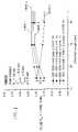
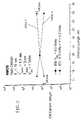
- FIG. 2is a graph showing the nominal device off-current (nA/ ⁇ m) vs. channel length (nm).
- the present inventionwhich provides a method for statically biasing the back-gates or the body nodes of MOSFETs to obtain system high performance, while maintaining low system standby power, will now be described with reference to the drawings that accompany the present application.
- the drawingsrepresent one possible implementation of the present invention.
- the present inventionprovides a method for statically biasing the back-gates or the body nodes of MOSFETs to obtain system high performance, while maintaining low system standby power.
- the inventive methodis based on the use of the back-gate or the body node of an MOSFET to compensate MOSFET device threshold roll-off which is caused by variations in device parameters during fabrication of the transistors.
- the inventive methodologyis based on adjusting the threshold voltage during processing by first assuming that each transistor has its nominal maximum channel length and implanting into the channel region of each transistor. After manufacturing, additional adjustments in threshold voltage is made to those devices not meeting a pre-selected off-current value by biasing the back-gates or the body nodes of those transistors.
- the inventive method of threshold voltage compensationbegins with first designing a semiconductor chip or semiconductor system that includes a plurality of transistor devices that have a channel length equal to the nominal channel length value.
- the transistor devices formed in the present inventionare either back-gate devices or devices that include a body node (i.e., n-well or p-well).
- the transistorsare typically MOSFETs that include a gate conductor, at least one gate dielectric, and a channel region located beneath the gate conductor.
- back-gate devicesare formed utilizing techniques well known to those skilled in the art.
- One such process of forming a back-gated deviceis disclosed, for example, in U.S. patent application Ser. No. 10/639,942, filed Aug. 13, 2002, the contents of which are incorporated herein by reference.
- Back-gate devicesare typically characterized as MOSFET devices having a front gate and a back gate that are separated from a Si channel by gate dielectrics.
- the devices containing body nodesare formed utilizing conventional complementary metal oxide semiconductor (CMOS) processing schemes that are well known to those skilled in the art.
- CMOScomplementary metal oxide semiconductor
- the body node devicesare generally characterized as a bulk MOSFET device in which the substrate node can be biased to adjust the device threshold.
- the channel lengthranges in value from a nominal minimum value to a nominal maximum value. This variation in channel length is due to process variations that exist during the fabrication of each transistor.
- the nominal value of transistor channel length, L nomis based on the technology being used. For today's technology, the nominal channel length is 25 nm. Because of process variations however, the transistors have a channel length that can vary from 17.5 nm (nominal minimum) to 32.5 nm (nominal maximum). Those transistors that have channel lengths above nominal are referred to long channel devices, while the transistors that have channel lengths less than nominal are referred to as short channel devices.
- the threshold voltage of longer channel devicesis typically greater than the threshold voltage of shorter channel devices.
- the longer channel deviceshave a lower off-current than the off-current of shorter channel devices. Consequently, a methodology is needed to compensation for the variation in threshold voltage that can exists in a semiconductor chip or system.
- the threshold voltage of the transistor devicesis compensated (i.e., adjusted) by first assuming that each transistor device has its nominal maximum channel length and then implanting into the channel region such that each transistor device has substantially the same threshold voltage of about Vt min and an off-current that meets a preselected specification of about I-off max .
- the threshold voltage achieved after this compensation stepmay vary from semiconductor chip to semiconductor chip. Typically, however, the threshold voltage that is achieved after the compensating step is from about 50 to about 450 millivolts, with a threshold voltage from about 100 to about 150 millivolts being more typical.
- the off-current achieved after the compensating stepmay vary from semiconductor chip to semiconductor chip. Typical values of off-current that can be achieved after the compensating step are from about 50 to about 150 nA/ ⁇ m, with an off-current after compensation of about 100 nA/ ⁇ m being more typical. Although these ranges for off-current are specifically provided, the present invention can be used to achieve any preselected off-current that may be required.
- the threshold voltage of any long channel deviceswould be compensated by lower the threshold voltage of those transistors such that the long channel devices have a threshold voltage that is substantially equal to the threshold voltage of the short channel devices.
- the off-current of those transistor devicesis also increased to a value that substantially matches that of the short channel devices.
- the threshold voltage of the transistor devicesis compensated by implanting either an n-or p-type dopant into the channel region of each device.
- Suitable n-type dopants that can be employed in the present inventioninclude, but are not limited to Group V dopants such as, for example, As, Sb, and/or P, while suitable p-type dopants that are employed in the present invention include Group III dopants such as B.
- the degree of compensationcan be controlled by preselecting the implant conditions and the ion dosage used in this embodiment of the present invention.
- the implant conditions employed in the presentmay vary over wide ranges and are dependent upon the ion that is being implanted and the degree of threshold voltage adjustment needed.
- Typical implant conditions that can be used in the present inventionare as follows: implanting at an energy from about 5 to about 30 keV.
- the ion dosage that can be employed in the present inventionmay vary depending upon the degree of compensation required as well as the type of ion that is being implanted into the channel region of the longer channel devices.
- the ion dosage employed in the present inventioncan be from about 1E11 to about 1E13 atoms/cm 2 .
- the ion dosageis typically from about 1E11 to about 1E13 atoms/cm 2 .
- the threshold voltage of the transistor devices requiring further adjustingcan be made, during or after testing, by biasing the back-gate or the body node thereof.
- the biasingincreases the threshold voltage of shorter channel devices to a value such that the off-current thereof also increases.
- the biasing of the back-gates or body nodesmay be achieved by an external DC voltage source, an internal circuit that can deliver a potential to the back-gate or the body node of the second transistors or by an external clock system that can deliver a potential.
- the biasingcan be achieved by comparing the system clock to the output of an on-chip running oscillator.
- the use of the external clockhas the advantage of a temperature self-adjusting back bias voltage.
- CURVE X of FIG. 2shows the worst case process device off-current as a function of channel length that corresponds to the Vt roll-off characteristics shown in Curve B of FIG. 1 .
Landscapes
- Physics & Mathematics (AREA)
- Engineering & Computer Science (AREA)
- Computer Hardware Design (AREA)
- Computing Systems (AREA)
- General Engineering & Computer Science (AREA)
- Mathematical Physics (AREA)
- Metal-Oxide And Bipolar Metal-Oxide Semiconductor Integrated Circuits (AREA)
- Laser Surgery Devices (AREA)
- Surgical Instruments (AREA)
Abstract
Description
- 1) First, using proper channel implant dose, the threshold voltage of the longer channel devices are adjusted (Lchan=32.5 nm) to obtain the required off-current I-offmaxas shown in Curve D of
FIG. 1 and Curve X ofFIG. 2 . - 2) second, adjusting the back-gate bias for only the shorter devices (Lchan<32.5 nm) to increase their threshold voltage as shown in Curve D of
FIG. 1 . The threshold voltage shift Δ shown inFIG. 1 is chosen such that I-offmin(Curve Y ofFIG. 2 ) is equal I-offmaxunder worst case device variations condition. This back-gate bias can be supplied externally or generated on chip by comparing the system clock to the output of an on-chip free running oscillator. The later case has the advantage of a temperature self adjusting back-bias voltage.
Claims (13)
Priority Applications (2)
| Application Number | Priority Date | Filing Date | Title |
|---|---|---|---|
| US10/796,805US7089515B2 (en) | 2004-03-09 | 2004-03-09 | Threshold voltage roll-off compensation using back-gated MOSFET devices for system high-performance and low standby power |
| PCT/US2005/007630WO2005086824A2 (en) | 2004-03-09 | 2005-03-07 | High intensity ablation device |
Applications Claiming Priority (1)
| Application Number | Priority Date | Filing Date | Title |
|---|---|---|---|
| US10/796,805US7089515B2 (en) | 2004-03-09 | 2004-03-09 | Threshold voltage roll-off compensation using back-gated MOSFET devices for system high-performance and low standby power |
Publications (2)
| Publication Number | Publication Date |
|---|---|
| US20050204319A1 US20050204319A1 (en) | 2005-09-15 |
| US7089515B2true US7089515B2 (en) | 2006-08-08 |
Family
ID=34919935
Family Applications (1)
| Application Number | Title | Priority Date | Filing Date |
|---|---|---|---|
| US10/796,805Expired - Fee RelatedUS7089515B2 (en) | 2004-03-09 | 2004-03-09 | Threshold voltage roll-off compensation using back-gated MOSFET devices for system high-performance and low standby power |
Country Status (2)
| Country | Link |
|---|---|
| US (1) | US7089515B2 (en) |
| WO (1) | WO2005086824A2 (en) |
Cited By (59)
| Publication number | Priority date | Publication date | Assignee | Title |
|---|---|---|---|---|
| US20080316828A1 (en)* | 2007-06-21 | 2008-12-25 | Hanafi Hussein I | Memory in logic cell |
| US20090073782A1 (en)* | 2007-09-17 | 2009-03-19 | Micron Technology, Inc. | System, apparatus, and method to increase read and write stability of scaled sram memory cells |
| US20090072857A1 (en)* | 2007-09-14 | 2009-03-19 | Srinivas Perisetty | Integrated circuits with adjustable body bias and power supply circuitry |
| US20090321873A1 (en)* | 2008-06-30 | 2009-12-31 | Bich-Yen Nguyen | Low-cost substrates having high-resistivity properties and methods for their manufacture |
| US20090321872A1 (en)* | 2008-06-30 | 2009-12-31 | Bich-Yen Nguyen | Low cost substrates and method of forming such substrates |
| US20090321829A1 (en)* | 2008-06-30 | 2009-12-31 | Bich-Yen Nguyen | Low-cost double-structure substrates and methods for their manufacture |
| US8273617B2 (en) | 2009-09-30 | 2012-09-25 | Suvolta, Inc. | Electronic devices and systems, and methods for making and using the same |
| US8302064B1 (en)* | 2009-03-10 | 2012-10-30 | Xilinx, Inc. | Method of product performance improvement by selective feature sizing of semiconductor devices |
| US8377783B2 (en) | 2010-09-30 | 2013-02-19 | Suvolta, Inc. | Method for reducing punch-through in a transistor device |
| US8400219B2 (en) | 2011-03-24 | 2013-03-19 | Suvolta, Inc. | Analog circuits having improved transistors, and methods therefor |
| US8404551B2 (en) | 2010-12-03 | 2013-03-26 | Suvolta, Inc. | Source/drain extension control for advanced transistors |
| US8421162B2 (en) | 2009-09-30 | 2013-04-16 | Suvolta, Inc. | Advanced transistors with punch through suppression |
| US8461875B1 (en) | 2011-02-18 | 2013-06-11 | Suvolta, Inc. | Digital circuits having improved transistors, and methods therefor |
| US8525271B2 (en) | 2011-03-03 | 2013-09-03 | Suvolta, Inc. | Semiconductor structure with improved channel stack and method for fabrication thereof |
| US8530286B2 (en) | 2010-04-12 | 2013-09-10 | Suvolta, Inc. | Low power semiconductor transistor structure and method of fabrication thereof |
| US8569156B1 (en) | 2011-05-16 | 2013-10-29 | Suvolta, Inc. | Reducing or eliminating pre-amorphization in transistor manufacture |
| US8569128B2 (en) | 2010-06-21 | 2013-10-29 | Suvolta, Inc. | Semiconductor structure and method of fabrication thereof with mixed metal types |
| US8599623B1 (en) | 2011-12-23 | 2013-12-03 | Suvolta, Inc. | Circuits and methods for measuring circuit elements in an integrated circuit device |
| US8614128B1 (en) | 2011-08-23 | 2013-12-24 | Suvolta, Inc. | CMOS structures and processes based on selective thinning |
| US8629016B1 (en) | 2011-07-26 | 2014-01-14 | Suvolta, Inc. | Multiple transistor types formed in a common epitaxial layer by differential out-diffusion from a doped underlayer |
| US8637955B1 (en) | 2012-08-31 | 2014-01-28 | Suvolta, Inc. | Semiconductor structure with reduced junction leakage and method of fabrication thereof |
| US8645878B1 (en) | 2011-08-23 | 2014-02-04 | Suvolta, Inc. | Porting a circuit design from a first semiconductor process to a second semiconductor process |
| US8713511B1 (en) | 2011-09-16 | 2014-04-29 | Suvolta, Inc. | Tools and methods for yield-aware semiconductor manufacturing process target generation |
| US8735987B1 (en) | 2011-06-06 | 2014-05-27 | Suvolta, Inc. | CMOS gate stack structures and processes |
| US8748270B1 (en) | 2011-03-30 | 2014-06-10 | Suvolta, Inc. | Process for manufacturing an improved analog transistor |
| US8748986B1 (en) | 2011-08-05 | 2014-06-10 | Suvolta, Inc. | Electronic device with controlled threshold voltage |
| US8759872B2 (en) | 2010-06-22 | 2014-06-24 | Suvolta, Inc. | Transistor with threshold voltage set notch and method of fabrication thereof |
| US8796048B1 (en) | 2011-05-11 | 2014-08-05 | Suvolta, Inc. | Monitoring and measurement of thin film layers |
| US8811068B1 (en) | 2011-05-13 | 2014-08-19 | Suvolta, Inc. | Integrated circuit devices and methods |
| US8816754B1 (en) | 2012-11-02 | 2014-08-26 | Suvolta, Inc. | Body bias circuits and methods |
| US8819603B1 (en) | 2011-12-15 | 2014-08-26 | Suvolta, Inc. | Memory circuits and methods of making and designing the same |
| US8863064B1 (en) | 2012-03-23 | 2014-10-14 | Suvolta, Inc. | SRAM cell layout structure and devices therefrom |
| US8877619B1 (en) | 2012-01-23 | 2014-11-04 | Suvolta, Inc. | Process for manufacture of integrated circuits with different channel doping transistor architectures and devices therefrom |
| US8883600B1 (en) | 2011-12-22 | 2014-11-11 | Suvolta, Inc. | Transistor having reduced junction leakage and methods of forming thereof |
| US8895327B1 (en) | 2011-12-09 | 2014-11-25 | Suvolta, Inc. | Tipless transistors, short-tip transistors, and methods and circuits therefor |
| US8970289B1 (en) | 2012-01-23 | 2015-03-03 | Suvolta, Inc. | Circuits and devices for generating bi-directional body bias voltages, and methods therefor |
| US8976575B1 (en) | 2013-08-29 | 2015-03-10 | Suvolta, Inc. | SRAM performance monitor |
| US8988153B1 (en) | 2013-03-09 | 2015-03-24 | Suvolta, Inc. | Ring oscillator with NMOS or PMOS variation insensitivity |
| US8995204B2 (en) | 2011-06-23 | 2015-03-31 | Suvolta, Inc. | Circuit devices and methods having adjustable transistor body bias |
| US8994415B1 (en) | 2013-03-01 | 2015-03-31 | Suvolta, Inc. | Multiple VDD clock buffer |
| US8999861B1 (en) | 2011-05-11 | 2015-04-07 | Suvolta, Inc. | Semiconductor structure with substitutional boron and method for fabrication thereof |
| US9041126B2 (en) | 2012-09-21 | 2015-05-26 | Mie Fujitsu Semiconductor Limited | Deeply depleted MOS transistors having a screening layer and methods thereof |
| US9054219B1 (en) | 2011-08-05 | 2015-06-09 | Mie Fujitsu Semiconductor Limited | Semiconductor devices having fin structures and fabrication methods thereof |
| US9070477B1 (en) | 2012-12-12 | 2015-06-30 | Mie Fujitsu Semiconductor Limited | Bit interleaved low voltage static random access memory (SRAM) and related methods |
| US9093550B1 (en) | 2012-01-31 | 2015-07-28 | Mie Fujitsu Semiconductor Limited | Integrated circuits having a plurality of high-K metal gate FETs with various combinations of channel foundation structure and gate stack structure and methods of making same |
| US9093997B1 (en) | 2012-11-15 | 2015-07-28 | Mie Fujitsu Semiconductor Limited | Slew based process and bias monitors and related methods |
| US9112484B1 (en) | 2012-12-20 | 2015-08-18 | Mie Fujitsu Semiconductor Limited | Integrated circuit process and bias monitors and related methods |
| US9112057B1 (en) | 2012-09-18 | 2015-08-18 | Mie Fujitsu Semiconductor Limited | Semiconductor devices with dopant migration suppression and method of fabrication thereof |
| US9112495B1 (en) | 2013-03-15 | 2015-08-18 | Mie Fujitsu Semiconductor Limited | Integrated circuit device body bias circuits and methods |
| US9236466B1 (en) | 2011-10-07 | 2016-01-12 | Mie Fujitsu Semiconductor Limited | Analog circuits having improved insulated gate transistors, and methods therefor |
| US9268885B1 (en) | 2013-02-28 | 2016-02-23 | Mie Fujitsu Semiconductor Limited | Integrated circuit device methods and models with predicted device metric variations |
| US9299801B1 (en) | 2013-03-14 | 2016-03-29 | Mie Fujitsu Semiconductor Limited | Method for fabricating a transistor device with a tuned dopant profile |
| US9299698B2 (en) | 2012-06-27 | 2016-03-29 | Mie Fujitsu Semiconductor Limited | Semiconductor structure with multiple transistors having various threshold voltages |
| US9319013B2 (en) | 2014-08-19 | 2016-04-19 | Mie Fujitsu Semiconductor Limited | Operational amplifier input offset correction with transistor threshold voltage adjustment |
| US9406567B1 (en) | 2012-02-28 | 2016-08-02 | Mie Fujitsu Semiconductor Limited | Method for fabricating multiple transistor devices on a substrate with varying threshold voltages |
| US9431068B2 (en) | 2012-10-31 | 2016-08-30 | Mie Fujitsu Semiconductor Limited | Dynamic random access memory (DRAM) with low variation transistor peripheral circuits |
| US9449967B1 (en) | 2013-03-15 | 2016-09-20 | Fujitsu Semiconductor Limited | Transistor array structure |
| US9478571B1 (en) | 2013-05-24 | 2016-10-25 | Mie Fujitsu Semiconductor Limited | Buried channel deeply depleted channel transistor |
| US9710006B2 (en) | 2014-07-25 | 2017-07-18 | Mie Fujitsu Semiconductor Limited | Power up body bias circuits and methods |
Families Citing this family (7)
| Publication number | Priority date | Publication date | Assignee | Title |
|---|---|---|---|---|
| US7296247B1 (en)* | 2004-08-17 | 2007-11-13 | Xilinx, Inc. | Method and apparatus to improve pass transistor performance |
| US7454738B2 (en)* | 2005-06-10 | 2008-11-18 | Purdue Research Foundation | Synthesis approach for active leakage power reduction using dynamic supply gating |
| EP2015681B1 (en) | 2006-05-03 | 2018-03-28 | Datascope Corp. | Tissue closure device |
| WO2015077356A1 (en) | 2013-11-19 | 2015-05-28 | Wheeler William K | Fastener applicator with interlock |
| US11127738B2 (en)* | 2018-02-09 | 2021-09-21 | Xcelsis Corporation | Back biasing of FD-SOI circuit blocks |
| JP7348199B2 (en) | 2018-03-28 | 2023-09-20 | データスコープ コーポレイション | Device for atrial appendage exclusion |
| US11004953B2 (en) | 2019-06-26 | 2021-05-11 | Globalfoundries U.S. Inc. | Mask-free methods of forming structures in a semiconductor device |
Citations (5)
| Publication number | Priority date | Publication date | Assignee | Title |
|---|---|---|---|---|
| US4260909A (en)* | 1978-08-30 | 1981-04-07 | Bell Telephone Laboratories, Incorporated | Back gate bias voltage generator circuit |
| US4542485A (en)* | 1981-01-14 | 1985-09-17 | Tokyo Shibaura Denki Kabushiki Kaisha | Semiconductor integrated circuit |
| US5622880A (en)* | 1994-08-18 | 1997-04-22 | Sun Microsystems, Inc. | Method of making a low power, high performance junction transistor |
| US6023641A (en)* | 1998-04-29 | 2000-02-08 | Medtronic, Inc. | Power consumption reduction in medical devices employing multiple digital signal processors |
| US6472919B1 (en)* | 2001-06-01 | 2002-10-29 | Sun Microsystems, Inc. | Low voltage latch with uniform stack height |
Family Cites Families (6)
| Publication number | Priority date | Publication date | Assignee | Title |
|---|---|---|---|---|
| US4240431A (en)* | 1977-05-16 | 1980-12-23 | Olympus Optical Co., Ltd. | Laser knife |
| US4872456A (en)* | 1987-11-12 | 1989-10-10 | Hasson Harrith M | Template incision device |
| US5322055B1 (en)* | 1993-01-27 | 1997-10-14 | Ultracision Inc | Clamp coagulator/cutting system for ultrasonic surgical instruments |
| US5626607A (en)* | 1995-04-03 | 1997-05-06 | Heartport, Inc. | Clamp assembly and method of use |
| US6953461B2 (en)* | 2002-05-16 | 2005-10-11 | Tissuelink Medical, Inc. | Fluid-assisted medical devices, systems and methods |
| AU2002248196A1 (en)* | 2000-12-15 | 2002-08-12 | Tony R. Brown | Atrial fibrillation rf treatment device and method |
- 2004
- 2004-03-09USUS10/796,805patent/US7089515B2/ennot_activeExpired - Fee Related
- 2005
- 2005-03-07WOPCT/US2005/007630patent/WO2005086824A2/enactiveApplication Filing
Patent Citations (5)
| Publication number | Priority date | Publication date | Assignee | Title |
|---|---|---|---|---|
| US4260909A (en)* | 1978-08-30 | 1981-04-07 | Bell Telephone Laboratories, Incorporated | Back gate bias voltage generator circuit |
| US4542485A (en)* | 1981-01-14 | 1985-09-17 | Tokyo Shibaura Denki Kabushiki Kaisha | Semiconductor integrated circuit |
| US5622880A (en)* | 1994-08-18 | 1997-04-22 | Sun Microsystems, Inc. | Method of making a low power, high performance junction transistor |
| US6023641A (en)* | 1998-04-29 | 2000-02-08 | Medtronic, Inc. | Power consumption reduction in medical devices employing multiple digital signal processors |
| US6472919B1 (en)* | 2001-06-01 | 2002-10-29 | Sun Microsystems, Inc. | Low voltage latch with uniform stack height |
Cited By (135)
| Publication number | Priority date | Publication date | Assignee | Title |
|---|---|---|---|---|
| US20100055871A1 (en)* | 2007-06-21 | 2010-03-04 | Micron Technology, Inc. | Memory in logic cell |
| US7633801B2 (en) | 2007-06-21 | 2009-12-15 | Micron Technology, Inc. | Memory in logic cell |
| US20080316828A1 (en)* | 2007-06-21 | 2008-12-25 | Hanafi Hussein I | Memory in logic cell |
| US8367505B2 (en) | 2007-06-21 | 2013-02-05 | Micron Technology, Inc. | Memory in logic cell |
| US20090072857A1 (en)* | 2007-09-14 | 2009-03-19 | Srinivas Perisetty | Integrated circuits with adjustable body bias and power supply circuitry |
| US7675317B2 (en) | 2007-09-14 | 2010-03-09 | Altera Corporation | Integrated circuits with adjustable body bias and power supply circuitry |
| US20090073782A1 (en)* | 2007-09-17 | 2009-03-19 | Micron Technology, Inc. | System, apparatus, and method to increase read and write stability of scaled sram memory cells |
| US7613031B2 (en) | 2007-09-17 | 2009-11-03 | Micron Technology, Inc. | System, apparatus, and method to increase read and write stability of scaled SRAM memory cells |
| US20090321873A1 (en)* | 2008-06-30 | 2009-12-31 | Bich-Yen Nguyen | Low-cost substrates having high-resistivity properties and methods for their manufacture |
| US20090321829A1 (en)* | 2008-06-30 | 2009-12-31 | Bich-Yen Nguyen | Low-cost double-structure substrates and methods for their manufacture |
| US20090321872A1 (en)* | 2008-06-30 | 2009-12-31 | Bich-Yen Nguyen | Low cost substrates and method of forming such substrates |
| US20110042780A1 (en)* | 2008-06-30 | 2011-02-24 | S.O.I Tec Silicon On Insulator Technologies | Methods of manufacturing semiconductor structures and semiconductor structures obtained by such methods |
| US7977705B2 (en) | 2008-06-30 | 2011-07-12 | S.O.I.Tec Silicon On Insulator Technologies | Low-cost substrates having high-resistivity properties and methods for their manufacture |
| US8013417B2 (en) | 2008-06-30 | 2011-09-06 | S.O.I.T.ec Silicon on Insulator Technologies | Low cost substrates and method of forming such substrates |
| US8035163B2 (en) | 2008-06-30 | 2011-10-11 | S.O.I.Tec Silicon On Insulator Technologies | Low-cost double-structure substrates and methods for their manufacture |
| US20110037150A1 (en)* | 2008-06-30 | 2011-02-17 | Bich-Yen Nguyen | Substrate comprising different types of surfaces and method for obtaining such substrates |
| US8302064B1 (en)* | 2009-03-10 | 2012-10-30 | Xilinx, Inc. | Method of product performance improvement by selective feature sizing of semiconductor devices |
| US9263523B2 (en) | 2009-09-30 | 2016-02-16 | Mie Fujitsu Semiconductor Limited | Advanced transistors with punch through suppression |
| US10325986B2 (en) | 2009-09-30 | 2019-06-18 | Mie Fujitsu Semiconductor Limited | Advanced transistors with punch through suppression |
| US10217668B2 (en) | 2009-09-30 | 2019-02-26 | Mie Fujitsu Semiconductor Limited | Electronic devices and systems, and methods for making and using the same |
| US10074568B2 (en) | 2009-09-30 | 2018-09-11 | Mie Fujitsu Semiconductor Limited | Electronic devices and systems, and methods for making and using same |
| US8421162B2 (en) | 2009-09-30 | 2013-04-16 | Suvolta, Inc. | Advanced transistors with punch through suppression |
| US10224244B2 (en) | 2009-09-30 | 2019-03-05 | Mie Fujitsu Semiconductor Limited | Electronic devices and systems, and methods for making and using the same |
| US8975128B2 (en) | 2009-09-30 | 2015-03-10 | Suvolta, Inc. | Electronic devices and systems, and methods for making and using the same |
| US8604527B2 (en) | 2009-09-30 | 2013-12-10 | Suvolta, Inc. | Electronic devices and systems, and methods for making and using the same |
| US8541824B2 (en) | 2009-09-30 | 2013-09-24 | Suvolta, Inc. | Electronic devices and systems, and methods for making and using the same |
| US11062950B2 (en) | 2009-09-30 | 2021-07-13 | United Semiconductor Japan Co., Ltd. | Electronic devices and systems, and methods for making and using the same |
| US9508800B2 (en) | 2009-09-30 | 2016-11-29 | Mie Fujitsu Semiconductor Limited | Advanced transistors with punch through suppression |
| US8273617B2 (en) | 2009-09-30 | 2012-09-25 | Suvolta, Inc. | Electronic devices and systems, and methods for making and using the same |
| US11887895B2 (en) | 2009-09-30 | 2024-01-30 | United Semiconductor Japan Co., Ltd. | Electronic devices and systems, and methods for making and using the same |
| US8604530B2 (en) | 2009-09-30 | 2013-12-10 | Suvolta, Inc. | Electronic devices and systems, and methods for making and using the same |
| US8530286B2 (en) | 2010-04-12 | 2013-09-10 | Suvolta, Inc. | Low power semiconductor transistor structure and method of fabrication thereof |
| US9496261B2 (en) | 2010-04-12 | 2016-11-15 | Mie Fujitsu Semiconductor Limited | Low power semiconductor transistor structure and method of fabrication thereof |
| US9865596B2 (en) | 2010-04-12 | 2018-01-09 | Mie Fujitsu Semiconductor Limited | Low power semiconductor transistor structure and method of fabrication thereof |
| US8569128B2 (en) | 2010-06-21 | 2013-10-29 | Suvolta, Inc. | Semiconductor structure and method of fabrication thereof with mixed metal types |
| US9224733B2 (en) | 2010-06-21 | 2015-12-29 | Mie Fujitsu Semiconductor Limited | Semiconductor structure and method of fabrication thereof with mixed metal types |
| US9418987B2 (en) | 2010-06-22 | 2016-08-16 | Mie Fujitsu Semiconductor Limited | Transistor with threshold voltage set notch and method of fabrication thereof |
| US9922977B2 (en) | 2010-06-22 | 2018-03-20 | Mie Fujitsu Semiconductor Limited | Transistor with threshold voltage set notch and method of fabrication thereof |
| US8759872B2 (en) | 2010-06-22 | 2014-06-24 | Suvolta, Inc. | Transistor with threshold voltage set notch and method of fabrication thereof |
| US8377783B2 (en) | 2010-09-30 | 2013-02-19 | Suvolta, Inc. | Method for reducing punch-through in a transistor device |
| US8563384B2 (en) | 2010-12-03 | 2013-10-22 | Suvolta, Inc. | Source/drain extension control for advanced transistors |
| US9006843B2 (en) | 2010-12-03 | 2015-04-14 | Suvolta, Inc. | Source/drain extension control for advanced transistors |
| US8686511B2 (en) | 2010-12-03 | 2014-04-01 | Suvolta, Inc. | Source/drain extension control for advanced transistors |
| US8404551B2 (en) | 2010-12-03 | 2013-03-26 | Suvolta, Inc. | Source/drain extension control for advanced transistors |
| US10250257B2 (en) | 2011-02-18 | 2019-04-02 | Mie Fujitsu Semiconductor Limited | Digital circuits having improved transistors, and methods therefor |
| US8461875B1 (en) | 2011-02-18 | 2013-06-11 | Suvolta, Inc. | Digital circuits having improved transistors, and methods therefor |
| US9680470B2 (en) | 2011-02-18 | 2017-06-13 | Mie Fujitsu Semiconductor Limited | Digital circuits having improved transistors, and methods therefor |
| US9184750B1 (en) | 2011-02-18 | 2015-11-10 | Mie Fujitsu Semiconductor Limited | Digital circuits having improved transistors, and methods therefor |
| US9838012B2 (en) | 2011-02-18 | 2017-12-05 | Mie Fujitsu Semiconductor Limited | Digital circuits having improved transistors, and methods therefor |
| US9985631B2 (en) | 2011-02-18 | 2018-05-29 | Mie Fujitsu Semiconductor Limited | Digital circuits having improved transistors, and methods therefor |
| US8525271B2 (en) | 2011-03-03 | 2013-09-03 | Suvolta, Inc. | Semiconductor structure with improved channel stack and method for fabrication thereof |
| US9111785B2 (en) | 2011-03-03 | 2015-08-18 | Mie Fujitsu Semiconductor Limited | Semiconductor structure with improved channel stack and method for fabrication thereof |
| US8847684B2 (en) | 2011-03-24 | 2014-09-30 | Suvolta, Inc. | Analog circuits having improved transistors, and methods therefor |
| US8400219B2 (en) | 2011-03-24 | 2013-03-19 | Suvolta, Inc. | Analog circuits having improved transistors, and methods therefor |
| US9231541B2 (en) | 2011-03-24 | 2016-01-05 | Mie Fujitsu Semiconductor Limited | Analog circuits having improved transistors, and methods therefor |
| US9093469B2 (en) | 2011-03-30 | 2015-07-28 | Mie Fujitsu Semiconductor Limited | Analog transistor |
| US8748270B1 (en) | 2011-03-30 | 2014-06-10 | Suvolta, Inc. | Process for manufacturing an improved analog transistor |
| US8796048B1 (en) | 2011-05-11 | 2014-08-05 | Suvolta, Inc. | Monitoring and measurement of thin film layers |
| US8999861B1 (en) | 2011-05-11 | 2015-04-07 | Suvolta, Inc. | Semiconductor structure with substitutional boron and method for fabrication thereof |
| US9362291B1 (en) | 2011-05-13 | 2016-06-07 | Mie Fujitsu Semiconductor Limited | Integrated circuit devices and methods |
| US9966130B2 (en) | 2011-05-13 | 2018-05-08 | Mie Fujitsu Semiconductor Limited | Integrated circuit devices and methods |
| US9741428B2 (en) | 2011-05-13 | 2017-08-22 | Mie Fujitsu Semiconductor Limited | Integrated circuit devices and methods |
| US8811068B1 (en) | 2011-05-13 | 2014-08-19 | Suvolta, Inc. | Integrated circuit devices and methods |
| US8569156B1 (en) | 2011-05-16 | 2013-10-29 | Suvolta, Inc. | Reducing or eliminating pre-amorphization in transistor manufacture |
| US8937005B2 (en) | 2011-05-16 | 2015-01-20 | Suvolta, Inc. | Reducing or eliminating pre-amorphization in transistor manufacture |
| US9514940B2 (en) | 2011-05-16 | 2016-12-06 | Mie Fujitsu Semiconductor Limited | Reducing or eliminating pre-amorphization in transistor manufacture |
| US9793172B2 (en) | 2011-05-16 | 2017-10-17 | Mie Fujitsu Semiconductor Limited | Reducing or eliminating pre-amorphization in transistor manufacture |
| US9508728B2 (en) | 2011-06-06 | 2016-11-29 | Mie Fujitsu Semiconductor Limited | CMOS gate stack structures and processes |
| US9281248B1 (en) | 2011-06-06 | 2016-03-08 | Mie Fujitsu Semiconductor Limited | CMOS gate stack structures and processes |
| US8735987B1 (en) | 2011-06-06 | 2014-05-27 | Suvolta, Inc. | CMOS gate stack structures and processes |
| US8995204B2 (en) | 2011-06-23 | 2015-03-31 | Suvolta, Inc. | Circuit devices and methods having adjustable transistor body bias |
| US8653604B1 (en) | 2011-07-26 | 2014-02-18 | Suvolta, Inc. | Multiple transistor types formed in a common epitaxial layer by differential out-diffusion from a doped underlayer |
| US8629016B1 (en) | 2011-07-26 | 2014-01-14 | Suvolta, Inc. | Multiple transistor types formed in a common epitaxial layer by differential out-diffusion from a doped underlayer |
| US8916937B1 (en) | 2011-07-26 | 2014-12-23 | Suvolta, Inc. | Multiple transistor types formed in a common epitaxial layer by differential out-diffusion from a doped underlayer |
| US8963249B1 (en) | 2011-08-05 | 2015-02-24 | Suvolta, Inc. | Electronic device with controlled threshold voltage |
| US9054219B1 (en) | 2011-08-05 | 2015-06-09 | Mie Fujitsu Semiconductor Limited | Semiconductor devices having fin structures and fabrication methods thereof |
| US8748986B1 (en) | 2011-08-05 | 2014-06-10 | Suvolta, Inc. | Electronic device with controlled threshold voltage |
| US8614128B1 (en) | 2011-08-23 | 2013-12-24 | Suvolta, Inc. | CMOS structures and processes based on selective thinning |
| US8645878B1 (en) | 2011-08-23 | 2014-02-04 | Suvolta, Inc. | Porting a circuit design from a first semiconductor process to a second semiconductor process |
| US9391076B1 (en) | 2011-08-23 | 2016-07-12 | Mie Fujitsu Semiconductor Limited | CMOS structures and processes based on selective thinning |
| US9117746B1 (en) | 2011-08-23 | 2015-08-25 | Mie Fujitsu Semiconductor Limited | Porting a circuit design from a first semiconductor process to a second semiconductor process |
| US8806395B1 (en) | 2011-08-23 | 2014-08-12 | Suvolta, Inc. | Porting a circuit design from a first semiconductor process to a second semiconductor process |
| US8713511B1 (en) | 2011-09-16 | 2014-04-29 | Suvolta, Inc. | Tools and methods for yield-aware semiconductor manufacturing process target generation |
| US9236466B1 (en) | 2011-10-07 | 2016-01-12 | Mie Fujitsu Semiconductor Limited | Analog circuits having improved insulated gate transistors, and methods therefor |
| US10573644B2 (en) | 2011-12-09 | 2020-02-25 | Mie Fujitsu Semiconductor Limited | Tipless transistors, short-tip transistors, and methods and circuits therefor |
| US9385121B1 (en) | 2011-12-09 | 2016-07-05 | Mie Fujitsu Semiconductor Limited | Tipless transistors, short-tip transistors, and methods and circuits therefor |
| US9953974B2 (en) | 2011-12-09 | 2018-04-24 | Mie Fujitsu Semiconductor Limited | Tipless transistors, short-tip transistors, and methods and circuits therefor |
| US8895327B1 (en) | 2011-12-09 | 2014-11-25 | Suvolta, Inc. | Tipless transistors, short-tip transistors, and methods and circuits therefor |
| US9583484B2 (en) | 2011-12-09 | 2017-02-28 | Mie Fujitsu Semiconductor Limited | Tipless transistors, short-tip transistors, and methods and circuits therefor |
| US11145647B2 (en) | 2011-12-09 | 2021-10-12 | United Semiconductor Japan Co., Ltd. | Tipless transistors, short-tip transistors, and methods and circuits therefor |
| US8819603B1 (en) | 2011-12-15 | 2014-08-26 | Suvolta, Inc. | Memory circuits and methods of making and designing the same |
| US8883600B1 (en) | 2011-12-22 | 2014-11-11 | Suvolta, Inc. | Transistor having reduced junction leakage and methods of forming thereof |
| US9196727B2 (en) | 2011-12-22 | 2015-11-24 | Mie Fujitsu Semiconductor Limited | High uniformity screen and epitaxial layers for CMOS devices |
| US9368624B2 (en) | 2011-12-22 | 2016-06-14 | Mie Fujitsu Semiconductor Limited | Method for fabricating a transistor with reduced junction leakage current |
| US8599623B1 (en) | 2011-12-23 | 2013-12-03 | Suvolta, Inc. | Circuits and methods for measuring circuit elements in an integrated circuit device |
| US9297850B1 (en) | 2011-12-23 | 2016-03-29 | Mie Fujitsu Semiconductor Limited | Circuits and methods for measuring circuit elements in an integrated circuit device |
| US8970289B1 (en) | 2012-01-23 | 2015-03-03 | Suvolta, Inc. | Circuits and devices for generating bi-directional body bias voltages, and methods therefor |
| US8877619B1 (en) | 2012-01-23 | 2014-11-04 | Suvolta, Inc. | Process for manufacture of integrated circuits with different channel doping transistor architectures and devices therefrom |
| US9093550B1 (en) | 2012-01-31 | 2015-07-28 | Mie Fujitsu Semiconductor Limited | Integrated circuits having a plurality of high-K metal gate FETs with various combinations of channel foundation structure and gate stack structure and methods of making same |
| US9385047B2 (en) | 2012-01-31 | 2016-07-05 | Mie Fujitsu Semiconductor Limited | Integrated circuits having a plurality of high-K metal gate FETs with various combinations of channel foundation structure and gate stack structure and methods of making same |
| US9406567B1 (en) | 2012-02-28 | 2016-08-02 | Mie Fujitsu Semiconductor Limited | Method for fabricating multiple transistor devices on a substrate with varying threshold voltages |
| US9424385B1 (en) | 2012-03-23 | 2016-08-23 | Mie Fujitsu Semiconductor Limited | SRAM cell layout structure and devices therefrom |
| US8863064B1 (en) | 2012-03-23 | 2014-10-14 | Suvolta, Inc. | SRAM cell layout structure and devices therefrom |
| US10014387B2 (en) | 2012-06-27 | 2018-07-03 | Mie Fujitsu Semiconductor Limited | Semiconductor structure with multiple transistors having various threshold voltages |
| US10217838B2 (en) | 2012-06-27 | 2019-02-26 | Mie Fujitsu Semiconductor Limited | Semiconductor structure with multiple transistors having various threshold voltages |
| US9812550B2 (en) | 2012-06-27 | 2017-11-07 | Mie Fujitsu Semiconductor Limited | Semiconductor structure with multiple transistors having various threshold voltages |
| US9299698B2 (en) | 2012-06-27 | 2016-03-29 | Mie Fujitsu Semiconductor Limited | Semiconductor structure with multiple transistors having various threshold voltages |
| US8637955B1 (en) | 2012-08-31 | 2014-01-28 | Suvolta, Inc. | Semiconductor structure with reduced junction leakage and method of fabrication thereof |
| US9105711B2 (en) | 2012-08-31 | 2015-08-11 | Mie Fujitsu Semiconductor Limited | Semiconductor structure with reduced junction leakage and method of fabrication thereof |
| US9112057B1 (en) | 2012-09-18 | 2015-08-18 | Mie Fujitsu Semiconductor Limited | Semiconductor devices with dopant migration suppression and method of fabrication thereof |
| US9041126B2 (en) | 2012-09-21 | 2015-05-26 | Mie Fujitsu Semiconductor Limited | Deeply depleted MOS transistors having a screening layer and methods thereof |
| US9431068B2 (en) | 2012-10-31 | 2016-08-30 | Mie Fujitsu Semiconductor Limited | Dynamic random access memory (DRAM) with low variation transistor peripheral circuits |
| US8816754B1 (en) | 2012-11-02 | 2014-08-26 | Suvolta, Inc. | Body bias circuits and methods |
| US9154123B1 (en) | 2012-11-02 | 2015-10-06 | Mie Fujitsu Semiconductor Limited | Body bias circuits and methods |
| US9093997B1 (en) | 2012-11-15 | 2015-07-28 | Mie Fujitsu Semiconductor Limited | Slew based process and bias monitors and related methods |
| US9319034B2 (en) | 2012-11-15 | 2016-04-19 | Mie Fujitsu Semiconductor Limited | Slew based process and bias monitors and related methods |
| US9070477B1 (en) | 2012-12-12 | 2015-06-30 | Mie Fujitsu Semiconductor Limited | Bit interleaved low voltage static random access memory (SRAM) and related methods |
| US9112484B1 (en) | 2012-12-20 | 2015-08-18 | Mie Fujitsu Semiconductor Limited | Integrated circuit process and bias monitors and related methods |
| US9276561B2 (en) | 2012-12-20 | 2016-03-01 | Mie Fujitsu Semiconductor Limited | Integrated circuit process and bias monitors and related methods |
| US9268885B1 (en) | 2013-02-28 | 2016-02-23 | Mie Fujitsu Semiconductor Limited | Integrated circuit device methods and models with predicted device metric variations |
| US8994415B1 (en) | 2013-03-01 | 2015-03-31 | Suvolta, Inc. | Multiple VDD clock buffer |
| US8988153B1 (en) | 2013-03-09 | 2015-03-24 | Suvolta, Inc. | Ring oscillator with NMOS or PMOS variation insensitivity |
| US9299801B1 (en) | 2013-03-14 | 2016-03-29 | Mie Fujitsu Semiconductor Limited | Method for fabricating a transistor device with a tuned dopant profile |
| US9577041B2 (en) | 2013-03-14 | 2017-02-21 | Mie Fujitsu Semiconductor Limited | Method for fabricating a transistor device with a tuned dopant profile |
| US9893148B2 (en) | 2013-03-14 | 2018-02-13 | Mie Fujitsu Semiconductor Limited | Method for fabricating a transistor device with a tuned dopant profile |
| US9548086B2 (en) | 2013-03-15 | 2017-01-17 | Mie Fujitsu Semiconductor Limited | Integrated circuit device body bias circuits and methods |
| US9112495B1 (en) | 2013-03-15 | 2015-08-18 | Mie Fujitsu Semiconductor Limited | Integrated circuit device body bias circuits and methods |
| US9449967B1 (en) | 2013-03-15 | 2016-09-20 | Fujitsu Semiconductor Limited | Transistor array structure |
| US9853019B2 (en) | 2013-03-15 | 2017-12-26 | Mie Fujitsu Semiconductor Limited | Integrated circuit device body bias circuits and methods |
| US9991300B2 (en) | 2013-05-24 | 2018-06-05 | Mie Fujitsu Semiconductor Limited | Buried channel deeply depleted channel transistor |
| US9478571B1 (en) | 2013-05-24 | 2016-10-25 | Mie Fujitsu Semiconductor Limited | Buried channel deeply depleted channel transistor |
| US9786703B2 (en) | 2013-05-24 | 2017-10-10 | Mie Fujitsu Semiconductor Limited | Buried channel deeply depleted channel transistor |
| US8976575B1 (en) | 2013-08-29 | 2015-03-10 | Suvolta, Inc. | SRAM performance monitor |
| US9710006B2 (en) | 2014-07-25 | 2017-07-18 | Mie Fujitsu Semiconductor Limited | Power up body bias circuits and methods |
| US9319013B2 (en) | 2014-08-19 | 2016-04-19 | Mie Fujitsu Semiconductor Limited | Operational amplifier input offset correction with transistor threshold voltage adjustment |
Also Published As
| Publication number | Publication date |
|---|---|
| WO2005086824A2 (en) | 2005-09-22 |
| WO2005086824A3 (en) | 2006-04-20 |
| US20050204319A1 (en) | 2005-09-15 |
Similar Documents
| Publication | Publication Date | Title |
|---|---|---|
| US7089515B2 (en) | Threshold voltage roll-off compensation using back-gated MOSFET devices for system high-performance and low standby power | |
| US6072217A (en) | Tunable threshold SOI device using isolated well structure for back gate | |
| US6436748B1 (en) | Method for fabricating CMOS transistors having matching characteristics and apparatus formed thereby | |
| US5942781A (en) | Tunable threshold SOI device using back gate well | |
| US6100567A (en) | Tunable threshold SOI device using back gate and intrinsic channel region | |
| US5917219A (en) | Semiconductor devices with pocket implant and counter doping | |
| US6496056B1 (en) | Process-tolerant integrated circuit design | |
| US5985705A (en) | Low threshold voltage MOS transistor and method of manufacture | |
| US5164805A (en) | Near-intrinsic thin-film SOI FETS | |
| EP0946990B1 (en) | Mos device having a gate to body connection formed on a soi substrate | |
| US6556068B2 (en) | Threshold voltage compensation circuits for low voltage and low power CMOS integrated circuits | |
| US5838189A (en) | Substrate voltage generating circuit of semiconductor memory device | |
| US6963100B2 (en) | Semiconductor device having gate electrode in which depletion layer can be generated | |
| US10026753B2 (en) | Method for compensating for temperature effects in semiconductor device structures using a diode structure and a tunable resistor | |
| US5672995A (en) | High speed mis-type intergrated circuit with self-regulated back bias | |
| US6693331B2 (en) | Method of fabricating dual threshold voltage n-channel and p-channel MOSFETS with a single extra masked implant operation | |
| US20110025285A1 (en) | Power supply voltage controlling circuit for use in subthreshold digital cmos circuit including minute current generator and controlled output voltage generator circuit | |
| US10079597B1 (en) | Circuit tuning scheme for FDSOI | |
| US6674127B2 (en) | Semiconductor integrated circuit | |
| US20060138543A1 (en) | Silicon-on-sapphire semiconductor device with shallow lightly-doped drain | |
| US6735072B2 (en) | On-chip decoupling capacitors designed for a 0.11 micron and beyond dual gate oxide CMOS technology | |
| US5602410A (en) | Off-state gate-oxide field reduction in CMOS | |
| Roy et al. | Leakage control for deep-submicron circuits | |
| JP4389065B2 (en) | SOI-MOSFET | |
| Chatterjee et al. | Pass transistor designs using pocket implant to improve manufacturability for 256 Mbit DRAM and beyond |
Legal Events
| Date | Code | Title | Description |
|---|---|---|---|
| AS | Assignment | Owner name:INTERNATIONAL BUSINESS MACHINES CORPORATION, NEW Y Free format text:ASSIGNMENT OF ASSIGNORS INTEREST;ASSIGNORS:HANAFI, HUSSEIN I.;DENNARD, ROBERT H.;HAENSCH, WILFRIED E.;REEL/FRAME:015094/0987 Effective date:20040302 | |
| AS | Assignment | Owner name:ETHICON, INC., NEW JERSEY Free format text:ASSIGNMENT OF ASSIGNORS INTEREST;ASSIGNORS:PENDEKANTI, RAJESH;PODANY, VACLAV O.;REEL/FRAME:015381/0217;SIGNING DATES FROM 20041005 TO 20041027 | |
| FEPP | Fee payment procedure | Free format text:PAYOR NUMBER ASSIGNED (ORIGINAL EVENT CODE: ASPN); ENTITY STATUS OF PATENT OWNER: LARGE ENTITY | |
| FPAY | Fee payment | Year of fee payment:4 | |
| REMI | Maintenance fee reminder mailed | ||
| FPAY | Fee payment | Year of fee payment:8 | |
| SULP | Surcharge for late payment | Year of fee payment:7 | |
| AS | Assignment | Owner name:GLOBALFOUNDRIES U.S. 2 LLC, NEW YORK Free format text:ASSIGNMENT OF ASSIGNORS INTEREST;ASSIGNOR:INTERNATIONAL BUSINESS MACHINES CORPORATION;REEL/FRAME:036550/0001 Effective date:20150629 | |
| AS | Assignment | Owner name:GLOBALFOUNDRIES INC., CAYMAN ISLANDS Free format text:ASSIGNMENT OF ASSIGNORS INTEREST;ASSIGNORS:GLOBALFOUNDRIES U.S. 2 LLC;GLOBALFOUNDRIES U.S. INC.;REEL/FRAME:036779/0001 Effective date:20150910 | |
| FEPP | Fee payment procedure | Free format text:MAINTENANCE FEE REMINDER MAILED (ORIGINAL EVENT CODE: REM.) | |
| LAPS | Lapse for failure to pay maintenance fees | Free format text:PATENT EXPIRED FOR FAILURE TO PAY MAINTENANCE FEES (ORIGINAL EVENT CODE: EXP.); ENTITY STATUS OF PATENT OWNER: LARGE ENTITY | |
| STCH | Information on status: patent discontinuation | Free format text:PATENT EXPIRED DUE TO NONPAYMENT OF MAINTENANCE FEES UNDER 37 CFR 1.362 | |
| FP | Lapsed due to failure to pay maintenance fee | Effective date:20180808 | |
| AS | Assignment | Owner name:GLOBALFOUNDRIES U.S. INC., NEW YORK Free format text:RELEASE BY SECURED PARTY;ASSIGNOR:WILMINGTON TRUST, NATIONAL ASSOCIATION;REEL/FRAME:056987/0001 Effective date:20201117 |