US7089436B2 - Power saving method and arrangement for a configurable processor array - Google Patents
Power saving method and arrangement for a configurable processor arrayDownload PDFInfo
- Publication number
- US7089436B2 US7089436B2US09/776,981US77698101AUS7089436B2US 7089436 B2US7089436 B2US 7089436B2US 77698101 AUS77698101 AUS 77698101AUS 7089436 B2US7089436 B2US 7089436B2
- Authority
- US
- United States
- Prior art keywords
- cells
- array
- row
- column
- mask
- Prior art date
- Legal status (The legal status is an assumption and is not a legal conclusion. Google has not performed a legal analysis and makes no representation as to the accuracy of the status listed.)
- Expired - Lifetime, expires
Links
Images

Classifications
- G—PHYSICS
- G06—COMPUTING OR CALCULATING; COUNTING
- G06F—ELECTRIC DIGITAL DATA PROCESSING
- G06F15/00—Digital computers in general; Data processing equipment in general
- G06F15/76—Architectures of general purpose stored program computers
- G06F15/78—Architectures of general purpose stored program computers comprising a single central processing unit
- G06F15/7867—Architectures of general purpose stored program computers comprising a single central processing unit with reconfigurable architecture
- G—PHYSICS
- G06—COMPUTING OR CALCULATING; COUNTING
- G06F—ELECTRIC DIGITAL DATA PROCESSING
- G06F1/00—Details not covered by groups G06F3/00 - G06F13/00 and G06F21/00
- G06F1/26—Power supply means, e.g. regulation thereof
- G06F1/32—Means for saving power
- G06F1/3203—Power management, i.e. event-based initiation of a power-saving mode
- G06F1/3234—Power saving characterised by the action undertaken
- G06F1/3237—Power saving characterised by the action undertaken by disabling clock generation or distribution
- G—PHYSICS
- G06—COMPUTING OR CALCULATING; COUNTING
- G06F—ELECTRIC DIGITAL DATA PROCESSING
- G06F1/00—Details not covered by groups G06F3/00 - G06F13/00 and G06F21/00
- G06F1/26—Power supply means, e.g. regulation thereof
- G06F1/32—Means for saving power
- G06F1/3203—Power management, i.e. event-based initiation of a power-saving mode
- G06F1/3234—Power saving characterised by the action undertaken
- G06F1/3287—Power saving characterised by the action undertaken by switching off individual functional units in the computer system
- G—PHYSICS
- G06—COMPUTING OR CALCULATING; COUNTING
- G06F—ELECTRIC DIGITAL DATA PROCESSING
- G06F15/00—Digital computers in general; Data processing equipment in general
- G06F15/76—Architectures of general purpose stored program computers
- G06F15/80—Architectures of general purpose stored program computers comprising an array of processing units with common control, e.g. single instruction multiple data processors
- G06F15/8007—Architectures of general purpose stored program computers comprising an array of processing units with common control, e.g. single instruction multiple data processors single instruction multiple data [SIMD] multiprocessors
- Y—GENERAL TAGGING OF NEW TECHNOLOGICAL DEVELOPMENTS; GENERAL TAGGING OF CROSS-SECTIONAL TECHNOLOGIES SPANNING OVER SEVERAL SECTIONS OF THE IPC; TECHNICAL SUBJECTS COVERED BY FORMER USPC CROSS-REFERENCE ART COLLECTIONS [XRACs] AND DIGESTS
- Y02—TECHNOLOGIES OR APPLICATIONS FOR MITIGATION OR ADAPTATION AGAINST CLIMATE CHANGE
- Y02D—CLIMATE CHANGE MITIGATION TECHNOLOGIES IN INFORMATION AND COMMUNICATION TECHNOLOGIES [ICT], I.E. INFORMATION AND COMMUNICATION TECHNOLOGIES AIMING AT THE REDUCTION OF THEIR OWN ENERGY USE
- Y02D10/00—Energy efficient computing, e.g. low power processors, power management or thermal management
Definitions
- the present inventionrelates generally to computer processors. More specifically, the present invention relates to power savings with an array structure of processor cells.
- a processing cellcontains logic elements for executing an operation on data according to an instruction. Increasingly, larger numbers of processing cells are connected together in one processor to accomplish a greater number of more complex processing tasks. For instance, a processor having cells that are arranged in an array of M rows and N columns is capable of processing M ⁇ N operations during each clock cycle. Further, each cell in the array can be individually programmed to perform a unique operation, such that the processor could accomplish M ⁇ N different operations during a single clock cycle.
- dynamic power consumptiondominates a system's overall power consumption.
- Each cellconsumes dynamic power in two ways: when its input is changing, and when its internal registers are clocked.
- Some processing applicationsrequire only a portion of the number of cells in a processor to execute a particular function.
- a cell that is not being used for a certain applicationwill still consume dynamic power by having its registers continually clocked while it awaits to be enabled.
- processorssuch as in a handheld computing device or wireless communication device for example, benefit from reduced power consumption.
- Reduced power consumptionallows for a smaller power supply, and thus a more efficient design of such devices.
- a device with reduced processor power consumptioncan achieve a longer battery life. Accordingly, there exists a need for a method and arrangement for saving power in a processor.
- an M ⁇ N array of processor cellsincludes control and logic circuitry for dynamic reconfiguration of individual cells, whereby a subset of cells is masked and enabled and the remaining unmasked cells are disabled.
- the enabled cellsare activated to accomplish a processing application, and the disabled cells do not consume dynamic power. In this manner, power consumption for the array is reduced, depending on the application.
- This inventionembodied as a method, includes the steps of providing a row mask signal configured to enable selected cells in each row of the array, and providing a column mask signal configured to enable selected cells in each column of the array.
- the methodfurther includes the step of gating the row mask signal and column mask signal with a clock signal of each cell to activate, at the next clock cycle, the enabled cells in the array based on the row mask signal and column mask signal.
- a method for saving power in an M ⁇ N array of processor cellsincludes masking the array to enable a subset of cells of the array, activating each enabled cell to execute the context instruction, and disabling each unmasked cell in the array, such that each disabled cell does not consume dynamic power.
- a power-saving arrangement for an M ⁇ N array of processor cellsincludes a row mask register configured to provide a row mask signal for enabling selected cells in each row of the array, and a column mask register configured to provide a column mask signal for enabling selected cells in each column of the array.
- the arrangementalso includes a clock circuit, connected to supply each cell with a clock signal, each clock signal being gated with the row mask signal and column mask signal to activate the enabled cells upon a new clock cycle.
- a power saving arrangement for an M ⁇ N array of processor cellsincludes a mask circuit for generating a mask signal for masking a portion of the cells in the array, and a clock for providing a clock signal, the clock signal being gated with the mask signal to activate the masked cells upon a new clock cycle.
- Selectively enabling and disabling cells in the arrayconfigures the array for a particular processing application, yet reduces power consumption depending on the application by powering only enabled and activated cells, and preventing dynamic power from being consumed by disabled cells.
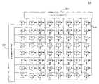
- FIG. 1shows a dynamically reconfigurable processing architecture including an M ⁇ N array of reconfigurable cells.
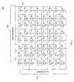
- FIG. 2depicts an M ⁇ N array of reconfigurable cells with enable registers.
- FIG. 3illustrates an internal structure of one reconfigurable cell according to an embodiment of the invention.
- power consumption by an array of processor cellscan be inefficiently large. Even while a particular cell is not actively processing data, the cell may still have its registers clocked and/or inputs changing. Reducing power consumption by a processor is an important goal toward achieving smaller power supplies, both physically and electrically for the processor. In such a case, the processor's utility in certain applications is enhanced.
- FIG. 1shows a dynamically reconfigurable processing structure 100 suitable for use with embodiments of the invention.
- the processing structure 100includes an M row ⁇ N column array of reconfigurable cells 110 .
- the M ⁇ N arrayis an 8 ⁇ 8 array of cells 110 .
- Each cell 110includes reconfigurable processing and logic elements which, when programmed, execute one or more logical functions.
- Each row Mis connected to a row context memory 120 .
- the row context memory 120provides the configuration data to instruct all cells 110 in each row.
- Each column Nis connected to a column context memory 130 .
- the column context memoryis configured to provide instructions to all cells 110 in each column.
- a row context from the row context memory 120is gated with a column context from the column context memory 130 at each cell 110 , to address and instruct the particular cell 110 .
- FIG. 2shows a processor array 200 with an arrangement for reducing power consumption in the array, according to an embodiment of the invention.
- An M-bit row mask register 310is connected to the cells 110 in each row of the M ⁇ N array.
- An N-bit column mask register 320is connected to the cells 110 in each column of the M ⁇ N array.
- a M-bit word from the row mask registeris combined with an N-bit word from the column mask register to mask a portion of the cells in the array 200 .
- the masked portion of cellsis enabled for operation, while the remaining unmasked cells are disabled.
- the disabled cellsare effectively switched off and do not consume dynamic power while the masked cells are activated and operate.
- the maskcan be updated at each cycle, if needed.
- both corresponding bit lines from the row and column mask registers 210 and 220must carry a logically active signal, such as a logical “1” for example, depending on a desired convention.
- FIG. 3illustrates the internal structure of one cell 110 .
- the cell 110includes one or more functional units 310 , 320 and 330 . While cell 100 is shown as having three functional units, the number of functional units is merely exemplary, and those having skill in the art would recognize that any combination of functional units can be used within the teachings of the present invention.
- a combination of active functional units 310 , 320 and/or 330defines an operation of the cell, and represents a logical function executed by the cell 110 during a processing cycle.
- Suitable functional unitscan include, without limitation, a Multiply-and-Accumulate (MAC) functional unit, an arithmetic unit, and a logic unit. Other types of functional units for performing functions are possible.
- MACMultiply-and-Accumulate
- the functional units 310 , 320 and/or 330are configured within the cell 110 in a modular fashion, in which functional units can be added or removed without needing to reconfigure the entire cell 110 .
- a range of operations of the cell 110is expandable and scalable.
- the modular design of the exemplary embodimentalso makes decoding of the function easier.
- the functional unitsare controlled and activated by a context register 340 .
- the context register 340latches a context instruction from the row context memory or the column context memory upon each processing cycle, and provides the configuration data to the appropriate functional unit(s). Depending upon the structure and logic of the group of functional units, and based on the context of the cell, more than one functional unit can be activated at a time.
- Each cell 110contains a storage register 312 for temporarily storing the functional unit computation results.
- the data output of the shifter 306is also provided to the storage register 312 , where it is temporarily stored until replaced by a new set of output data from the functional units 310 , 320 and/or 330 .
- the output register 316sends the output data to an output multiplexer 318 , from which the output data, representing a processing result of the reconfigurable cell, is sent to either the data bus, to a neighboring cell, or both.
- a row mask signal and a column mask signalare gated with a clock signal at AND gate 303 , for controlling all of the sequential logic elements within the cell 110 .
- the row mask signal and the column mask signalis gated at AND gate 307 , for activating transition barriers 311 , 321 , and 331 , which in turn prevent input changes from propagating to the internal components.
- all the clocks to the registers, including the context register 340are disabled. As a result, no dynamic power is consumed in the cell and the cell does not process any data.
- the row mask signal and the column signalthus control the flow of data to be operated upon by the cell 110 .
- the row mask signal and the column mask signalare provided by the row and column mask registers 210 and 220 , respectively as shown in FIG. 2 .
- the reconfigurable cells in an arrayare interconnected according to one or more hierarchical schemes.
- cells within a quadranti.e. each group of 4 ⁇ 4 cells, are fully connected in a row or column.
- cells in adjacent quadrantsare connected via specially-configured fast lanes that enable a cell in one quadrant to broadcast function results to all cells in an adjacent quadrant.
- the subset of cells that are masked and enabledmay follow some hierarchical scheme, or can be randomly or programmatically enabled.
Landscapes
- Engineering & Computer Science (AREA)
- Theoretical Computer Science (AREA)
- General Engineering & Computer Science (AREA)
- Physics & Mathematics (AREA)
- General Physics & Mathematics (AREA)
- Computer Hardware Design (AREA)
- Computing Systems (AREA)
- Logic Circuits (AREA)
Abstract
Description
Claims (15)
Priority Applications (1)
| Application Number | Priority Date | Filing Date | Title |
|---|---|---|---|
| US09/776,981US7089436B2 (en) | 2001-02-05 | 2001-02-05 | Power saving method and arrangement for a configurable processor array |
Applications Claiming Priority (1)
| Application Number | Priority Date | Filing Date | Title |
|---|---|---|---|
| US09/776,981US7089436B2 (en) | 2001-02-05 | 2001-02-05 | Power saving method and arrangement for a configurable processor array |
Publications (2)
| Publication Number | Publication Date |
|---|---|
| US20020108063A1 US20020108063A1 (en) | 2002-08-08 |
| US7089436B2true US7089436B2 (en) | 2006-08-08 |
Family
ID=25108917
Family Applications (1)
| Application Number | Title | Priority Date | Filing Date |
|---|---|---|---|
| US09/776,981Expired - LifetimeUS7089436B2 (en) | 2001-02-05 | 2001-02-05 | Power saving method and arrangement for a configurable processor array |
Country Status (1)
| Country | Link |
|---|---|
| US (1) | US7089436B2 (en) |
Cited By (3)
| Publication number | Priority date | Publication date | Assignee | Title |
|---|---|---|---|---|
| US20080046684A1 (en)* | 2006-08-17 | 2008-02-21 | International Business Machines Corporation | Multithreaded multicore uniprocessor and a heterogeneous multiprocessor incorporating the same |
| US20100191999A1 (en)* | 2009-01-23 | 2010-07-29 | Micron Technology, Inc. | Memory device power managers and methods |
| CN108628693A (en)* | 2018-04-17 | 2018-10-09 | 清华大学无锡应用技术研究院 | Processor debugging method and system |
Families Citing this family (5)
| Publication number | Priority date | Publication date | Assignee | Title |
|---|---|---|---|---|
| US20030007636A1 (en)* | 2001-06-25 | 2003-01-09 | Alves Vladimir Castro | Method and apparatus for executing a cryptographic algorithm using a reconfigurable datapath array |
| CN1720494A (en)* | 2002-12-04 | 2006-01-11 | 皇家飞利浦电子股份有限公司 | Register file gating method for reducing power consumption of microprocessor |
| CN101782893B (en)* | 2009-01-21 | 2014-12-24 | 上海芯豪微电子有限公司 | Reconfigurable data processing platform |
| US9501705B2 (en) | 2009-12-15 | 2016-11-22 | Micron Technology, Inc. | Methods and apparatuses for reducing power consumption in a pattern recognition processor |
| US11456855B2 (en)* | 2019-10-17 | 2022-09-27 | Arm Limited | Obfuscating data at-transit |
Citations (12)
| Publication number | Priority date | Publication date | Assignee | Title |
|---|---|---|---|---|
| US4907148A (en)* | 1985-11-13 | 1990-03-06 | Alcatel U.S.A. Corp. | Cellular array processor with individual cell-level data-dependent cell control and multiport input memory |
| US4920497A (en)* | 1987-10-27 | 1990-04-24 | State University Of New York | Method for rendering usuable a defective raw programmable logic array and a defective programmable logic array rendered usable by this method |
| JPH06103249A (en)* | 1992-09-22 | 1994-04-15 | Nippon Telegr & Teleph Corp <Ntt> | Processor array selection controller |
| US5615162A (en)* | 1995-01-04 | 1997-03-25 | Texas Instruments Incorporated | Selective power to memory |
| US5892729A (en)* | 1997-07-25 | 1999-04-06 | Lucent Technologies Inc. | Power savings for memory arrays |
| US5915123A (en) | 1997-10-31 | 1999-06-22 | Silicon Spice | Method and apparatus for controlling configuration memory contexts of processing elements in a network of multiple context processing elements |
| US6073185A (en) | 1993-08-27 | 2000-06-06 | Teranex, Inc. | Parallel data processor |
| US6108760A (en) | 1997-10-31 | 2000-08-22 | Silicon Spice | Method and apparatus for position independent reconfiguration in a network of multiple context processing elements |
| US6122719A (en) | 1997-10-31 | 2000-09-19 | Silicon Spice | Method and apparatus for retiming in a network of multiple context processing elements |
| US6205537B1 (en)* | 1998-07-16 | 2001-03-20 | University Of Rochester | Mechanism for dynamically adapting the complexity of a microprocessor |
| US6553525B1 (en)* | 1999-11-08 | 2003-04-22 | International Business Machines Corporation | Method and apparatus for selectively enabling and disabling functions on a per array basis |
| US6848058B1 (en)* | 1999-06-04 | 2005-01-25 | Ati International Srl | Power reduction circuit and method with multi clock branch control |
- 2001
- 2001-02-05USUS09/776,981patent/US7089436B2/ennot_activeExpired - Lifetime
Patent Citations (13)
| Publication number | Priority date | Publication date | Assignee | Title |
|---|---|---|---|---|
| US4907148A (en)* | 1985-11-13 | 1990-03-06 | Alcatel U.S.A. Corp. | Cellular array processor with individual cell-level data-dependent cell control and multiport input memory |
| US4920497A (en)* | 1987-10-27 | 1990-04-24 | State University Of New York | Method for rendering usuable a defective raw programmable logic array and a defective programmable logic array rendered usable by this method |
| JPH06103249A (en)* | 1992-09-22 | 1994-04-15 | Nippon Telegr & Teleph Corp <Ntt> | Processor array selection controller |
| US6073185A (en) | 1993-08-27 | 2000-06-06 | Teranex, Inc. | Parallel data processor |
| US5615162A (en)* | 1995-01-04 | 1997-03-25 | Texas Instruments Incorporated | Selective power to memory |
| US5986969A (en) | 1997-07-25 | 1999-11-16 | Lucent Technologies, Inc. | Power savings for memory arrays |
| US5892729A (en)* | 1997-07-25 | 1999-04-06 | Lucent Technologies Inc. | Power savings for memory arrays |
| US5915123A (en) | 1997-10-31 | 1999-06-22 | Silicon Spice | Method and apparatus for controlling configuration memory contexts of processing elements in a network of multiple context processing elements |
| US6108760A (en) | 1997-10-31 | 2000-08-22 | Silicon Spice | Method and apparatus for position independent reconfiguration in a network of multiple context processing elements |
| US6122719A (en) | 1997-10-31 | 2000-09-19 | Silicon Spice | Method and apparatus for retiming in a network of multiple context processing elements |
| US6205537B1 (en)* | 1998-07-16 | 2001-03-20 | University Of Rochester | Mechanism for dynamically adapting the complexity of a microprocessor |
| US6848058B1 (en)* | 1999-06-04 | 2005-01-25 | Ati International Srl | Power reduction circuit and method with multi clock branch control |
| US6553525B1 (en)* | 1999-11-08 | 2003-04-22 | International Business Machines Corporation | Method and apparatus for selectively enabling and disabling functions on a per array basis |
Cited By (6)
| Publication number | Priority date | Publication date | Assignee | Title |
|---|---|---|---|---|
| US20080046684A1 (en)* | 2006-08-17 | 2008-02-21 | International Business Machines Corporation | Multithreaded multicore uniprocessor and a heterogeneous multiprocessor incorporating the same |
| US20080209437A1 (en)* | 2006-08-17 | 2008-08-28 | International Business Machines Corporation | Multithreaded multicore uniprocessor and a heterogeneous multiprocessor incorporating the same |
| US20100191999A1 (en)* | 2009-01-23 | 2010-07-29 | Micron Technology, Inc. | Memory device power managers and methods |
| US9105323B2 (en)* | 2009-01-23 | 2015-08-11 | Micron Technology, Inc. | Memory device power managers and methods |
| US9583157B2 (en) | 2009-01-23 | 2017-02-28 | Micron Technology, Inc. | Memory device power managers and methods |
| CN108628693A (en)* | 2018-04-17 | 2018-10-09 | 清华大学无锡应用技术研究院 | Processor debugging method and system |
Also Published As
| Publication number | Publication date |
|---|---|
| US20020108063A1 (en) | 2002-08-08 |
Similar Documents
| Publication | Publication Date | Title |
|---|---|---|
| US20020133688A1 (en) | SIMD/MIMD processing on a reconfigurable array | |
| CN112083791B (en) | Chip power consumption optimization method, apparatus, computer equipment and storage medium | |
| US6745317B1 (en) | Three level direct communication connections between neighboring multiple context processing elements | |
| US8099618B2 (en) | Methods and devices for treating and processing data | |
| US20020188832A1 (en) | Method and apparatus for providing local control of processing elements in a network of multiple context processing elements | |
| US8122231B2 (en) | Software selectable adjustment of SIMD parallelism | |
| KR100806284B1 (en) | High Energy Efficiency Processor Using Dynamic Voltage Scaling | |
| US8341436B2 (en) | Method and system for power-state transition controllers | |
| US7089436B2 (en) | Power saving method and arrangement for a configurable processor array | |
| CN114239806B (en) | A multi-core neural network processor chip based on RISC-V architecture | |
| KR20070108932A (en) | Method and apparatus for power reduction in heterogeneous multi-pipeline processors | |
| US7861101B2 (en) | Reconfigurable signal processor | |
| US7906996B1 (en) | System and method for controlling an integrated circuit in different operational modes | |
| EP2310953B1 (en) | Improvements relating to single instruction multiple data (simd) architectures | |
| US5983339A (en) | Power down system and method for pipelined logic functions | |
| US20020112193A1 (en) | Power control of a processor using hardware structures controlled by a compiler with an accumulated instruction profile | |
| EP3841670B1 (en) | Reducing power consumption in a processor circuit | |
| CN110377348B (en) | Method and system for providing sleep to configurable logic block by intermittent energy-saving logic | |
| CN100385433C (en) | Apparatus and method for controlling rounding mode in a single instruction multiple data floating point unit | |
| KR100863080B1 (en) | Low-Power Configuration Cache and Reconfigurable Processing System Containing It | |
| US10331194B2 (en) | Methods and devices for treating and processing data | |
| US7290157B2 (en) | Configurable processor with main controller to increase activity of at least one of a plurality of processing units having local program counters | |
| US7668992B2 (en) | Context-based operation reconfigurable instruction set processor and method of operation | |
| CN116737651B (en) | Low-power-consumption memory computing architecture FPGA | |
| JP2005276854A (en) | Processing equipment |
Legal Events
| Date | Code | Title | Description |
|---|---|---|---|
| AS | Assignment | Owner name:MORPHO TECHNOLOGIES, CALIFORNIA Free format text:ASSIGNMENT OF ASSIGNORS INTEREST;ASSIGNORS:LEE, MING-HAU;KURDAHI, FADI;REEL/FRAME:011715/0598 Effective date:20010205 | |
| AS | Assignment | Owner name:SMART TECHNOLOGY VENTURES III SBIC, L.P., CALIFORN Free format text:ASSIGNMENT OF ASSIGNORS INTEREST;ASSIGNOR:MORPHO TECHNOLOGIES;REEL/FRAME:015550/0970 Effective date:20040615 Owner name:BRIDGEWEST, LLC, CALIFORNIA Free format text:ASSIGNMENT OF ASSIGNORS INTEREST;ASSIGNOR:MORPHO TECHNOLOGIES;REEL/FRAME:015550/0970 Effective date:20040615 Owner name:ELLUMINA, LLC, CALIFORNIA Free format text:ASSIGNMENT OF ASSIGNORS INTEREST;ASSIGNOR:MORPHO TECHNOLOGIES;REEL/FRAME:015550/0970 Effective date:20040615 Owner name:AMIRRA INVESTMENTS LTD., SAUDI ARABIA Free format text:ASSIGNMENT OF ASSIGNORS INTEREST;ASSIGNOR:MORPHO TECHNOLOGIES;REEL/FRAME:015550/0970 Effective date:20040615 Owner name:AMIR MOUSSAVIAN, CALIFORNIA Free format text:ASSIGNMENT OF ASSIGNORS INTEREST;ASSIGNOR:MORPHO TECHNOLOGIES;REEL/FRAME:015550/0970 Effective date:20040615 Owner name:MILAN INVESTMENTS, LP, CALIFORNIA Free format text:ASSIGNMENT OF ASSIGNORS INTEREST;ASSIGNOR:MORPHO TECHNOLOGIES;REEL/FRAME:015550/0970 Effective date:20040615 Owner name:LIBERTEL, LLC, CALIFORNIA Free format text:ASSIGNMENT OF ASSIGNORS INTEREST;ASSIGNOR:MORPHO TECHNOLOGIES;REEL/FRAME:015550/0970 Effective date:20040615 Owner name:BRIDGEWEST, LLC, CALIFORNIA Free format text:SECURITY INTEREST;ASSIGNOR:MORPHO TECHNOLOGIES;REEL/FRAME:015550/0970 Effective date:20040615 Owner name:ELLUMINA, LLC, CALIFORNIA Free format text:SECURITY INTEREST;ASSIGNOR:MORPHO TECHNOLOGIES;REEL/FRAME:015550/0970 Effective date:20040615 Owner name:LIBERTEL, LLC, CALIFORNIA Free format text:SECURITY INTEREST;ASSIGNOR:MORPHO TECHNOLOGIES;REEL/FRAME:015550/0970 Effective date:20040615 Owner name:MILAN INVESTMENTS, LP, CALIFORNIA Free format text:SECURITY INTEREST;ASSIGNOR:MORPHO TECHNOLOGIES;REEL/FRAME:015550/0970 Effective date:20040615 Owner name:AMIRRA INVESTMENTS LTD., SAUDI ARABIA Free format text:SECURITY INTEREST;ASSIGNOR:MORPHO TECHNOLOGIES;REEL/FRAME:015550/0970 Effective date:20040615 Owner name:AMIR MOUSSAVIAN, CALIFORNIA Free format text:SECURITY INTEREST;ASSIGNOR:MORPHO TECHNOLOGIES;REEL/FRAME:015550/0970 Effective date:20040615 Owner name:SMART TECHNOLOGY VENTURES III SBIC, L.P., CALIFORN Free format text:SECURITY INTEREST;ASSIGNOR:MORPHO TECHNOLOGIES;REEL/FRAME:015550/0970 Effective date:20040615 | |
| AS | Assignment | Owner name:MORPHO TECHNOLOGIES, INC., CALIFORNIA Free format text:RELEASE OF SECURITY AGREEMENT;ASSIGNORS:SMART TECHNOLOGY VENTURES III SBIC, L.P.;BRIDGE WEST, LLC;ELLUMINA, LLC;AND OTHERS;REEL/FRAME:016863/0843 Effective date:20040608 | |
| STCF | Information on status: patent grant | Free format text:PATENTED CASE | |
| FEPP | Fee payment procedure | Free format text:PAT HOLDER NO LONGER CLAIMS SMALL ENTITY STATUS, ENTITY STATUS SET TO UNDISCOUNTED (ORIGINAL EVENT CODE: STOL); ENTITY STATUS OF PATENT OWNER: LARGE ENTITY | |
| AS | Assignment | Owner name:FINLASIN TECHNOLOGY LLC, DELAWARE Free format text:ASSIGNMENT OF ASSIGNORS INTEREST;ASSIGNOR:MORPHO TECHNOLOGIES, INC.;REEL/FRAME:021876/0560 Effective date:20081009 | |
| FPAY | Fee payment | Year of fee payment:4 | |
| AS | Assignment | Owner name:MORPHO TECHNOLOGIES, CALIFORNIA Free format text:CORRECTION TO THE RECORDATION COVER SHEET OF THE RELEASE OF SECURITY AGREEMENT RECORDED AT 016863/0843 ON 8/9/2005;ASSIGNORS:SMART TECHNOLOGY VENTURES III SBIC, L.P.;BRIDGE WEST, LLC;ELLUMINA, LLC;AND OTHERS;REEL/FRAME:030836/0209 Effective date:20050802 | |
| FPAY | Fee payment | Year of fee payment:8 | |
| AS | Assignment | Owner name:NYTELL SOFTWARE LLC, DELAWARE Free format text:MERGER;ASSIGNOR:FINLASIN TECHNOLOGY LLC;REEL/FRAME:037392/0653 Effective date:20150826 | |
| MAFP | Maintenance fee payment | Free format text:PAYMENT OF MAINTENANCE FEE, 12TH YEAR, LARGE ENTITY (ORIGINAL EVENT CODE: M1553) Year of fee payment:12 | |
| AS | Assignment | Owner name:MORPHO TECHNOLOGIES, CALIFORNIA Free format text:CORRECTIVE ASSIGNMENT TO CORRECT THE RECEIVING PARTY AND EXECUTION DATES PREVIOUSLY RECORDED AT REEL: 016863 FRAME: 0843. ASSIGNOR(S) HEREBY CONFIRMS THE RELEASE OF SECURITY AGREEMENT;ASSIGNORS:SMART TECHNOLOGY VENTURES III SBIC, L.P.;BRIDGEWEST, LLC;ELLUMINA, LLC;AND OTHERS;REEL/FRAME:048210/0534 Effective date:20050802 | |
| AS | Assignment | Owner name:INTELLECTUAL VENTURES ASSETS 186 LLC, DELAWARE Free format text:ASSIGNMENT OF ASSIGNORS INTEREST;ASSIGNOR:NYTELL SOFTWARE LLC;REEL/FRAME:062708/0535 Effective date:20221222 | |
| AS | Assignment | Owner name:INTELLECTUAL VENTURES ASSETS 186 LLC, DELAWARE Free format text:SECURITY INTEREST;ASSIGNOR:MIND FUSION, LLC;REEL/FRAME:063295/0001 Effective date:20230214 Owner name:INTELLECTUAL VENTURES ASSETS 191 LLC, DELAWARE Free format text:SECURITY INTEREST;ASSIGNOR:MIND FUSION, LLC;REEL/FRAME:063295/0001 Effective date:20230214 | |
| AS | Assignment | Owner name:MIND FUSION, LLC, WASHINGTON Free format text:ASSIGNMENT OF ASSIGNORS INTEREST;ASSIGNOR:INTELLECTUAL VENTURES ASSETS 186 LLC;REEL/FRAME:064271/0001 Effective date:20230214 |