US7088409B2 - Liquid crystal display apparatus - Google Patents
Liquid crystal display apparatusDownload PDFInfo
- Publication number
- US7088409B2 US7088409B2US11/135,828US13582805AUS7088409B2US 7088409 B2US7088409 B2US 7088409B2US 13582805 AUS13582805 AUS 13582805AUS 7088409 B2US7088409 B2US 7088409B2
- Authority
- US
- United States
- Prior art keywords
- liquid crystal
- layer
- retardation
- transmissive
- display unit
- Prior art date
- Legal status (The legal status is an assumption and is not a legal conclusion. Google has not performed a legal analysis and makes no representation as to the accuracy of the status listed.)
- Expired - Fee Related
Links
Images


Classifications
- G—PHYSICS
- G02—OPTICS
- G02F—OPTICAL DEVICES OR ARRANGEMENTS FOR THE CONTROL OF LIGHT BY MODIFICATION OF THE OPTICAL PROPERTIES OF THE MEDIA OF THE ELEMENTS INVOLVED THEREIN; NON-LINEAR OPTICS; FREQUENCY-CHANGING OF LIGHT; OPTICAL LOGIC ELEMENTS; OPTICAL ANALOGUE/DIGITAL CONVERTERS
- G02F1/00—Devices or arrangements for the control of the intensity, colour, phase, polarisation or direction of light arriving from an independent light source, e.g. switching, gating or modulating; Non-linear optics
- G02F1/01—Devices or arrangements for the control of the intensity, colour, phase, polarisation or direction of light arriving from an independent light source, e.g. switching, gating or modulating; Non-linear optics for the control of the intensity, phase, polarisation or colour
- G02F1/13—Devices or arrangements for the control of the intensity, colour, phase, polarisation or direction of light arriving from an independent light source, e.g. switching, gating or modulating; Non-linear optics for the control of the intensity, phase, polarisation or colour based on liquid crystals, e.g. single liquid crystal display cells
- G02F1/133—Constructional arrangements; Operation of liquid crystal cells; Circuit arrangements
- G02F1/1333—Constructional arrangements; Manufacturing methods
- G02F1/1335—Structural association of cells with optical devices, e.g. polarisers or reflectors
- G02F1/133553—Reflecting elements
- G02F1/133555—Transflectors
- G—PHYSICS
- G02—OPTICS
- G02F—OPTICAL DEVICES OR ARRANGEMENTS FOR THE CONTROL OF LIGHT BY MODIFICATION OF THE OPTICAL PROPERTIES OF THE MEDIA OF THE ELEMENTS INVOLVED THEREIN; NON-LINEAR OPTICS; FREQUENCY-CHANGING OF LIGHT; OPTICAL LOGIC ELEMENTS; OPTICAL ANALOGUE/DIGITAL CONVERTERS
- G02F1/00—Devices or arrangements for the control of the intensity, colour, phase, polarisation or direction of light arriving from an independent light source, e.g. switching, gating or modulating; Non-linear optics
- G02F1/01—Devices or arrangements for the control of the intensity, colour, phase, polarisation or direction of light arriving from an independent light source, e.g. switching, gating or modulating; Non-linear optics for the control of the intensity, phase, polarisation or colour
- G02F1/13—Devices or arrangements for the control of the intensity, colour, phase, polarisation or direction of light arriving from an independent light source, e.g. switching, gating or modulating; Non-linear optics for the control of the intensity, phase, polarisation or colour based on liquid crystals, e.g. single liquid crystal display cells
- G02F1/133—Constructional arrangements; Operation of liquid crystal cells; Circuit arrangements
- G02F1/1333—Constructional arrangements; Manufacturing methods
- G02F1/133371—Cells with varying thickness of the liquid crystal layer
- G—PHYSICS
- G02—OPTICS
- G02F—OPTICAL DEVICES OR ARRANGEMENTS FOR THE CONTROL OF LIGHT BY MODIFICATION OF THE OPTICAL PROPERTIES OF THE MEDIA OF THE ELEMENTS INVOLVED THEREIN; NON-LINEAR OPTICS; FREQUENCY-CHANGING OF LIGHT; OPTICAL LOGIC ELEMENTS; OPTICAL ANALOGUE/DIGITAL CONVERTERS
- G02F1/00—Devices or arrangements for the control of the intensity, colour, phase, polarisation or direction of light arriving from an independent light source, e.g. switching, gating or modulating; Non-linear optics
- G02F1/01—Devices or arrangements for the control of the intensity, colour, phase, polarisation or direction of light arriving from an independent light source, e.g. switching, gating or modulating; Non-linear optics for the control of the intensity, phase, polarisation or colour
- G02F1/13—Devices or arrangements for the control of the intensity, colour, phase, polarisation or direction of light arriving from an independent light source, e.g. switching, gating or modulating; Non-linear optics for the control of the intensity, phase, polarisation or colour based on liquid crystals, e.g. single liquid crystal display cells
- G02F1/133—Constructional arrangements; Operation of liquid crystal cells; Circuit arrangements
- G02F1/1333—Constructional arrangements; Manufacturing methods
- G02F1/1335—Structural association of cells with optical devices, e.g. polarisers or reflectors
- G02F1/13356—Structural association of cells with optical devices, e.g. polarisers or reflectors characterised by the placement of the optical elements
- G02F1/133565—Structural association of cells with optical devices, e.g. polarisers or reflectors characterised by the placement of the optical elements inside the LC elements, i.e. between the cell substrates
- G—PHYSICS
- G02—OPTICS
- G02F—OPTICAL DEVICES OR ARRANGEMENTS FOR THE CONTROL OF LIGHT BY MODIFICATION OF THE OPTICAL PROPERTIES OF THE MEDIA OF THE ELEMENTS INVOLVED THEREIN; NON-LINEAR OPTICS; FREQUENCY-CHANGING OF LIGHT; OPTICAL LOGIC ELEMENTS; OPTICAL ANALOGUE/DIGITAL CONVERTERS
- G02F1/00—Devices or arrangements for the control of the intensity, colour, phase, polarisation or direction of light arriving from an independent light source, e.g. switching, gating or modulating; Non-linear optics
- G02F1/01—Devices or arrangements for the control of the intensity, colour, phase, polarisation or direction of light arriving from an independent light source, e.g. switching, gating or modulating; Non-linear optics for the control of the intensity, phase, polarisation or colour
- G02F1/13—Devices or arrangements for the control of the intensity, colour, phase, polarisation or direction of light arriving from an independent light source, e.g. switching, gating or modulating; Non-linear optics for the control of the intensity, phase, polarisation or colour based on liquid crystals, e.g. single liquid crystal display cells
- G02F1/133—Constructional arrangements; Operation of liquid crystal cells; Circuit arrangements
- G02F1/1333—Constructional arrangements; Manufacturing methods
- G02F1/1335—Structural association of cells with optical devices, e.g. polarisers or reflectors
- G02F1/13363—Birefringent elements, e.g. for optical compensation
- G02F1/133631—Birefringent elements, e.g. for optical compensation with a spatial distribution of the retardation value
- G—PHYSICS
- G02—OPTICS
- G02F—OPTICAL DEVICES OR ARRANGEMENTS FOR THE CONTROL OF LIGHT BY MODIFICATION OF THE OPTICAL PROPERTIES OF THE MEDIA OF THE ELEMENTS INVOLVED THEREIN; NON-LINEAR OPTICS; FREQUENCY-CHANGING OF LIGHT; OPTICAL LOGIC ELEMENTS; OPTICAL ANALOGUE/DIGITAL CONVERTERS
- G02F1/00—Devices or arrangements for the control of the intensity, colour, phase, polarisation or direction of light arriving from an independent light source, e.g. switching, gating or modulating; Non-linear optics
- G02F1/01—Devices or arrangements for the control of the intensity, colour, phase, polarisation or direction of light arriving from an independent light source, e.g. switching, gating or modulating; Non-linear optics for the control of the intensity, phase, polarisation or colour
- G02F1/13—Devices or arrangements for the control of the intensity, colour, phase, polarisation or direction of light arriving from an independent light source, e.g. switching, gating or modulating; Non-linear optics for the control of the intensity, phase, polarisation or colour based on liquid crystals, e.g. single liquid crystal display cells
- G02F1/133—Constructional arrangements; Operation of liquid crystal cells; Circuit arrangements
- G02F1/1333—Constructional arrangements; Manufacturing methods
- G02F1/1343—Electrodes
- G02F1/134309—Electrodes characterised by their geometrical arrangement
- G02F1/134363—Electrodes characterised by their geometrical arrangement for applying an electric field parallel to the substrate, i.e. in-plane switching [IPS]
Definitions
- the inventionrelates to a liquid crystal display which can display images in a wide range of environment from a light place to a dark place and execute a transmissive display with a wide viewing angle and high picture quality.
- a transmissive liquid crystal display of an IPS (In Plane Switching) system, a VA (Vertical Alignment) system, or the likehas been spread as a monitor and is also used as a television by improving response performance.
- a liquid crystal displayhas also been spread to the fields of portable information apparatuses such as cellular phone and digital camera.
- portable information apparatusis mainly used personally, in recent years, the number of portable information apparatuses in which an inclination angle of a display unit can be varied has been increased and the display unit is often observed from the oblique direction. Therefore, a wide viewing angle is demanded.
- the display for the portable information apparatusis used in a variety of environments in ranges from the outdoors in the fine weather to the darkroom, it is demanded that the display is transflective.
- a reflective display unit and a transmissive display unitare arranged in one pixel.
- the reflective display unitperforms a display by reflecting a light entering from the ambience with use of a reflection layer and a contrast ratio is kept constant irrespective of the ambient brightness, so that a good display state can be obtained under a relatively light environment in ranges from the outdoors in the fine weather to the interior of the room.
- a contrast ratiois kept constant irrespective of the ambient brightness
- the transmissive display unitsince a backlight is used and the brightness is kept constant irrespective of the environment, a display of a high contrast ratio can be obtained in a relatively dark environment in ranges from the interior of the room to the darkroom.
- the transflective liquid crystal displayhaving functions of both of them, a display of the high contrast ratio can be obtained in a wide range of environment from the outdoors in the fine weather to the darkroom.
- the reflective display and the transmissive display of a wide viewing angleare simultaneously obtained by constructing the display of the IPS system known as a transmissive display of the wide viewing angle as a transflective type.
- the transflective IPS systemhas been disclosed in, for example, JP-A-11-242226.
- phase differences among the retardation filmshave viewing angle dependency. Therefore, even if the phase differences among the liquid crystal layer and the plurality of retardation films and an axis layout are optimized in a normal direction, as a viewing point gets away from the normal direction, conditions rapidly deteriorate to be away from optimum conditions for the dark display.
- the viewing angle dependency of the phase differencescan be reduced by adjusting a refractive index in the thickness direction of the retardation films, it cannot be completely eliminated.
- an increase in dark display transmissive ratio in the oblique directionis large and viewing angle performance of the transmissive display is inferior to that of the transmissive IPS system.
- the liquid crystal layerhas homogeneous alignment
- upper and lower polarization filmsare arranged so that their transmissive axes cross perpendicularly, and one of the transmissive axes is parallel with the liquid crystal alignment direction. Since the light entering the liquid crystal layer is linearly polarized light and its electric vector is parallel with the liquid crystal alignment direction, the phase differences are not obtained by the liquid crystal layer. Therefore, since a dark display of a low transmissive ratio can be realized and no retardation films exist between the liquid crystal layer and the polarization films, a surplus phase difference does not occur in the oblique direction and the dark display with the wide viewing angle can be realized. As mentioned above, the retardation films are inherently unnecessary in the transmissive IPS system.
- the reflective display unit and the transmissive display unit in which optical conditions for the dark display are essentially differentare arranged in one pixel. That is, in the reflective display unit, the light enters from the polarization film on the upper surface of the liquid crystal display, is reflected by the reflection layer in the liquid crystal panel, thereafter, passes through the upper polarization film again, and is directed toward the user. In the transmissive display unit, the light enters from the polarization film on the lower surface of the liquid crystal display, thereafter, passes through the polarization film on the upper surface of the liquid crystal display, and is directed toward the user.
- phase difference between the phase of the light which provides the dark display in the reflective display unit and that in the transmissive display unitis caused due to such a difference between optical paths and it is equal to a quarter wave. Therefore, when the reflective display unit is in the light display mode, the transmissive display unit is in the dark display mode or vice versa, and the reflective display unit and the transmissive display unit have different applied voltage dependency. To allow those display units to have the same applied voltage dependency, the phase difference between the reflective display unit and the transmissive display unit has to be shifted by the quarter wave by some method.
- the retardation filmsare arranged on the whole upper and lower surfaces of the liquid crystal panel.
- the light which enters the reflective display unit from the outside, the light reflected by the reflection layer of the reflective display unit, and the light which passed through the transmissive display unitpass through the retardation films on the upper side of the liquid crystal panel among those retardation films.
- the upper retardation filmsact on both of the reflective display unit and the transmissive display unit.
- the lower retardation filmsact only on the transmissive display unit.
- the phase difference between both of the display unitsis shifted by the quarter wave.
- the surplus phase differenceoccurs in the oblique direction since the retardation films exist between the liquid crystal layer and the polarization films, the viewing angle performance of the dark display deteriorates.
- retardation filmsare arranged only in a reflective display unit of the transflective IPS system and polarization films which are used for the reflective display unit and the transmissive display unit have common specifications.
- the polarization filmsare arranged on the whole upper and lower surfaces of a liquid crystal panel, and the retardation films are formed as an inner retardation layer in the liquid crystal panel, patterned, and formed only in the reflective display unit.
- the upper and lower polarization filmsin a manner similar to that in the transmissive IPS system (their transmissive axes perpendicularly cross each other and one of them is parallel with a liquid crystal alignment direction), the same transmissive display viewing angle performance as that of the transmissive IPS system is obtained.
- the inner retardation layeris arranged so as to shift a phase difference between the reflective display unit and the transmissive display unit by a quarter wave.
- a laminate of the liquid crystal layer and the inner retardation layeris arranged like a quarter wave plate of a wide band. That is, the retardation of one of them near the reflection layer is set to the quarter wave and that of the other is set to the half wave.
- a layout of the liquid crystal layeris changed so that mainly a director azimuth is rotated in the layer when a voltage is applied, a change in tilt angle is small, and the retardation hardly changes. Therefore, between the liquid crystal layer and the retardation films, the liquid crystal layer is arranged in close vicinity to a reflective electrode and its retardation is set to the quarter wave.
- a slow axis of the inner retardation layeris determined as follows. An azimuth is defined counterclockwise by setting a transmissive axis of the upper polarization film to 0°.
- a slow axis azimuth of the inner retardation layeris assumed to be ⁇ PH and an azimuth of the alignment direction of the liquid crystal layer is assumed to be ⁇ LC , an azimuth in the case of the quarter wave plate of the wide band is shown by the following expression (1).
- a method of obtaining the expression (1)will be described hereinafter.
- ⁇ PH⁇ 45°+ ⁇ LC (1)
- ⁇ LChas to be set to either 0° or ⁇ 90° since the layout of the polarization films in the transmissive display unit is similar to that of the transmissive IPS.
- ⁇ PHis equal to ⁇ 22.5° (a range from 20° or more to 25° or less in consideration of an allowance of ⁇ 10% in manufacturing) or ⁇ 67.5° (a range from 60° or more to 75° or less in consideration of an allowance of ⁇ 10% in manufacturing).
- the optimum values of the liquid crystal layer retardation to set the reflective ratio and the transmissive ratio to the maximum which is determined by light absorption of the polarization filmsare different.
- the optimum valueis set to the quarter wave.
- the transmissive display unitit is set to the half wave.
- a thickness of liquid crystal layer of the reflective display unithas to be set to be smaller than that of the transmissive display unit.
- a thickness adjustment layeris arranged in the reflective display unit and the thickness of liquid crystal layer of the reflective display unit is reduced by an amount corresponding to a thickness of thickness adjustment layer.
- the thickness adjustment layerhas to be arranged so as to correspond to the reflective display unit.
- the inner retardation layeris used, it is also arranged so as to correspond to the reflective display unit.
- a difference between the retardation necessary for the reflective display unit and the transmissive display unitis equal to the quarter wave and the retardation necessary for the inner retardation layer is equal to the half wave.
- a thickness of inner retardation layeris smaller than a difference between the liquid crystal layer thicknesses necessary for the reflective display unit and the transmissive display unit.
- the inner retardation layer and the thickness adjustment layerare laminated and patterned so as to correspond to the reflective display unit, and a total of the layer thicknesses of both of them is set to the liquid crystal layer thickness difference necessary for the reflective display unit and the transmissive display unit.
- the thickness of inner retardation layeris equal to the liquid crystal layer thickness difference necessary for the reflective display unit and the transmissive display unit. In this case, since the thickness adjustment layer is unnecessary, the manufacturing steps can be simplified.
- an all-environment type liquid crystal display with a wide viewing anglecan be realized. That is, an all-environment type display which can display in various environments ranging from the outdoors in the fine weather to the darkroom is realized and, in the transmissive display, the display of a wide viewing angle similar to that of a monitor is obtained.
- the display with high picture quality similar to that of the monitorcan be carried. If it is used as a display of a cellular phone, image information of high picture quality can be reconstructed and the more advanced image information can be handled. Further, if it is used for a digital camera, an image before photographing and the photographed image can be easily confirmed. It is also presumed that a receiving state of a portable television will be remarkably improved in future in association with the spread of terrestrial digital broadcasting. If it is used for a portable television, the image information of high picture quality can be reproduced in any place.
- FIG. 1is a diagram showing various lines and electrode distribution in one pixel on a second substrate of a liquid crystal display according to the embodiment 1;
- FIG. 2is a diagram showing a cross section of one pixel of the liquid crystal display of the embodiment 1;
- FIG. 3is a diagram showing a layout of axes in a transmissive display unit of the liquid crystal display of the embodiment 1;
- FIG. 4is a diagram showing a layout of axes in a reflective display unit of the liquid crystal display of the embodiment 1;
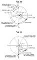
- FIG. 5is a display diagram of a Poincare' sphere showing a polarization converting function of retardation films and a liquid crystal layer in the reflective display unit;
- FIG. 6is a display diagram of the Poincare' sphere showing the polarization converting function of retardation films and a liquid crystal layer in the reflective display unit of the light on a short wavelength side among visible wavelengths;
- FIG. 7is a display diagram of the Poincare' sphere showing the polarization converting function of retardation films and a liquid crystal layer in the reflective display unit of the light on a long wavelength side among visible wavelengths;
- FIGS. 8A to 8Dare diagrams when FIGS. 5 and 9 are seen from the S3-axis direction;
- FIG. 9is a display diagram of the Poincare' sphere showing the polarization converting function of retardation films and a liquid crystal layer in the reflective display unit;
- FIG. 10is a graph showing viewing angle performance of a dark display transmissive ratio of the liquid crystal display of the embodiment 1;
- FIG. 11is a graph showing liquid crystal layer thickness dependency of the dark display transmissive ratio of the liquid crystal display of the embodiment 1;
- FIG. 12is a diagram showing a cross section of one pixel of a liquid crystal display of the embodiment 2;
- FIG. 13is a diagram showing various lines and electrode distribution in one pixel on a second substrate of a liquid crystal display according to the embodiment 3;
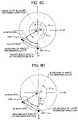
- FIG. 14is a diagram showing a layout of axes in a reflective display unit of the liquid crystal display of the embodiment 3;
- FIG. 15is a diagram showing a layout of axes in a transmissive display unit of the liquid crystal display of the embodiment 3;
- FIG. 16is a diagram showing various lines and electrode distribution in one pixel on a second substrate of a liquid crystal display according to the embodiment 4;
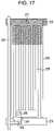
- FIG. 17is a diagram showing various lines and electrode distribution in one pixel on a second substrate of a liquid crystal display according to the embodiment 5;
- FIG. 18is a diagram showing a layout of axes in a reflective display unit of the liquid crystal display of the embodiment 5;
- FIG. 19is a diagram showing a layout of axes in a transmissive display unit of the liquid crystal display of the embodiment 5;
- FIG. 20is a diagram showing various lines and electrode distribution in one pixel on a second substrate of a liquid crystal display according to the embodiment 6;
- FIG. 21is a diagram showing a layout of axes in a reflective display unit of the liquid crystal display of the embodiment 6;
- FIG. 22is a diagram showing a layout of axes in a transmissive display unit of the liquid crystal display of the embodiment 6;
- FIG. 23is a diagram showing a cross section of one pixel of a liquid crystal display of the embodiment 7;
- FIG. 24is a graph showing viewing angle performance of a dark display transmissive ratio of the transmissive IPS liquid crystal display
- FIG. 25is a diagram showing a cross section of one pixel of a conventional liquid crystal display
- FIG. 26is a graph showing viewing angle performance of a dark display transmissive ratio of the conventional liquid crystal display.
- FIG. 27is a graph showing liquid crystal layer thickness dependency of the dark display transmissive ratio of the conventional liquid crystal display.
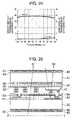
- FIG. 2A cross sectional view of one pixel constructing a liquid crystal display according to the invention is shown in FIG. 2 .
- a top view when a second substrate 32 is observed from the normal directionis shown in FIG. 1 .
- a cross sectional view taken along an alternate long and short dash line 1 - 2 shown in FIG. 1is also FIG. 2 .
- the liquid crystal display of the inventionis constructed mainly by a first substrate 31 , a liquid crystal layer 10 , and the second substrate 32 .
- the liquid crystal layer 10is sandwiched between the first substrate 31 and the second substrate 32 .
- the first substrate 31On the side near the liquid crystal layer 10 , the first substrate 31 has a color filter 36 , a leveling layer 37 , a third alignment layer 35 , an inner retardation layer 38 , and a first alignment layer 33 .
- the second substrate 32On the side near the liquid crystal layer 10 , the second substrate 32 has a thin film transistor.
- the thin film transistoris connected to a scanning line 21 , a signal line 22 , and a pixel electrode 28 . Besides them, the second substrate 32 has a common line 23 and a common electrode 29 .
- the thin film transistorhas an anti stagger structure and its channel portion is made of an amorphous silicon layer 25 .
- the scanning line 21 and the signal line 22cross each other and the thin film transistor is located approximately in such a crossing portion.
- the common line 23is distributed in parallel with the scanning line 21 and connected through a second through hole 27 .
- the pixel electrode 28 and the thin film transistorare coupled via a first through hole 26 .
- a second alignment layer 34is formed on the pixel electrode 28 and arranged in close vicinity to the liquid crystal layer 10 , thereby specifying its alignment direction.
- the first substrate 31is made of borosilicate glass hardly containing ionizable impurities and has a thickness of 0.5 mm.
- the color filter 36is constructed by repetitively arranging red, green, and blue portions in a stripe shape and each stripe is parallel with the signal line 22 . A rough surface caused by the color filter 36 is flattened by the leveling layer 37 made of a resin.
- the first alignment layer 33is a polyimide organic layer and is aligned by a rubbing method, thereby aligning the close liquid crystal layer 10 in the alignment processing direction.
- the second substrate 32is made of borosilicate glass and has a thickness of 0.5 mm in a manner similar to the first substrate 31 .
- the second alignment layer 34is a polyimide organic layer having horizontal alignment performance in a manner similar to the first alignment layer 33 .
- Each of the signal line 22 , the scanning line 21 , and the common line 23is made of chromium.
- the pixel electrode 28is transparent electrodes made of indium tin oxide (ITO). A part of the common electrode 29 is also made of ITO.
- the pixel electrode 28has slits 30 which are parallel with the scanning line 21 and a pitch of the slits 30 is equal to about 4 ⁇ m.
- the pixel electrode 28 and the common electrode 29are partitioned by a third insulation layer 53 having a thickness of 0.5 ⁇ m.
- the common line 23has a structure in which it is protruded into the pixel electrode 28 and reflects light as shown as reflective light 62 in FIG. 2 .
- the portion where the common line 23 is overlapped with the pixel electrode 28corresponds to the reflective display unit and other overlapped portion of the pixel electrode 28 and the common electrode 29 becomes a transmissive display unit which passes the light of the backlight as shown by transmissive light 61 in FIG. 2 . Since optimum liquid crystal layer thicknesses in the reflective display unit and the transmissive display unit are different, a step is formed at a boundary between them. To shorten the boundary between the transmissive display unit and the reflective display unit, the transmissive display unit and the reflective display unit are arranged so that the boundary is parallel with a short side of the pixel.
- the transmissive display portionis a portion that becomes transparent when the first substrate 31 is combined with the second substrate 32 so that the portion may pass the backlight and causes the liquid crystal layer 10 to be operated by the electric field applied thereon.
- the reflective display portionis a portion that becomes opaque when the first substrate 31 is combined with the second substrate 32 so that the portion may cut off the backlight, includes a metallic layer with a high reflectance so that the metallic layer may reflect ambient light, and causes the liquid crystal layer 10 to be operated by the electric field applied thereon.
- the linessuch as a common line 23 and the like are used in common for the reflection layer, the effect of reducing the manufacturing steps is obtained. If the common line 23 is made of aluminum with high reflective ratio, the brighter reflection display is obtained. A similar effect can be obtained even if the common line 23 is made of chromium and the reflection layer made of aluminum or silver alloy is separately formed.
- the liquid crystal layer 10is a liquid crystal composition showing positive dielectric constant anisotropy in which a dielectric constant in the alignment direction is larger than that in its normal direction. Its bireflingence is equal to 0.067 at 25° C. and the liquid crystal layer 10 exhibits a nematic phase in a temperature range including a room temperature region. For a holding period of time when the display is driven at a frequency of 60 Hz by using the thin film transistor, a high resistance value in which the sufficient reflective ratio and transmissive ratio are held and no flickers are caused is shown.
- the inner retardation layer 38is formed on the first substrate 31 where the color filter 36 and the leveling layer 37 have been formed. Its forming method is as follows.
- the third alignment layer 35 having the horizontal alignment performanceis coated onto the leveling layer 37 , baked, and subjected to an alignment process by the rubbing method.
- the third alignment layer 35has a function of determining a slow axis direction of the inner retardation layer 38 .
- An organic solvent containing a liquid crystal having a photoreactive acryl group at a molecule end and an initiatoris coated onto the third alignment layer 35 and heated, thereby removing the organic solvent.
- the photoreactive liquid crystalis aligned in the alignment processing direction of the third alignment layer 35 .
- the acryl groupis photopolymerized and a film is formed, thereby obtaining the inner retardation layer 38 .
- the film thicknessis adjusted by properly controlling a solution concentration and coating conditions upon coating, thereby setting the retardation of the inner retardation layer 38 to the half wave at a wavelength of 550 nm.
- the inner retardation layer 38is made of a liquid crystal polymer, its alignment performance of the molecules is higher than that of the retardation films formed by drawing an organic polymer film and the layer 38 has the alignment performance similar to that of the liquid crystal layer 10 . Therefore, ⁇ n of the inner retardation layer 38 is fairly larger than that of the externally attached retardation films and can be set to a value which is almost equal to or larger than that of the liquid crystal layer 10 by properly adjusting the molecular structure and film forming conditions.
- a thickness of externally attached retardation filmsis equal to tens of ⁇ m and is about ten times as that of the liquid crystal layer
- the thickness of inner retardation layer 38can be fairly reduced by using the liquid crystal polymer and be set to be thinner than the step between the reflective display unit and the transmissive display unit. Thus, even if the inner retardation layer 38 is patterned in accordance with the reflective display unit, the special leveling is unnecessary.
- the inner retardation layer 38is patterned so as to have distribution similar to that of the reflective display unit.
- a resistis coated onto the inner retardation layer 38 and patterned so as to have the distribution similar to that of the reflective display unit. After that, it is ashed with an oxygen plasma, thereby removing the inner retardation layer in the portion where the resist is not distributed.
- a shiftmay take place when the first substrate 31 is combined with the second substrate 32 .
- built-in phase plates 38may be distributed in the transparent portion of the second substrate. In this portion, when no voltage is applied, the built-in phase plates 38 serve to change the polarized state of the transmitted light and thereby generate the components to be transmitted through the first polarizer 41 . As a result, the backlight is passed therethrough, so that the transmittance may not be sufficiently reduced on the dark image and the contrast ratio of the transmissive display may be lowered.
- an area where no built-in phase plate 38 is distributedmay occur on the reflective electrode.
- the reflective electrodesince the light reaching the reflective plate is not made to be circularly polarized light, when the light is reflected on the reflective plate and again reaches the first polarizer 41 , the components that are allowed to pass through the first polarizer 41 are generated. As a result, the reflectance on the dark image is not sufficiently reduced and the contrast ratio in the reflective display is made lower.
- the distribution of the built-in phase plates 38is formed to be smaller than the reflective display portion as keeping the correspondence between the distribution and the reflective display portion. For example, in a case that it is presumed that the shift occurring in combining the first substrate 31 with the second substrate 32 is made to be 2 ⁇ m at maximum, the distribution of the built-in phase plates 38 is formed to be smaller by 2 ⁇ m than the reflective display portion. Even if the shift of the first substrate 31 to the second substrate 32 becomes the maximum, this formation makes it possible to prevent the built-in phase plates 38 from being distributed in the transparent portion of the second substrate and the contrast ratio in the transmissive display from being lowered.
- the contrast ratio of the transmissive displayis not made lower.
- the patterning accuracymay be improved. The improvement of the patterning accuracy leads to preventing distribution of the built-in phase plates 38 in the transmissive display portion.
- the thickness when the retardation of the inner retardation layer 38 is set to the half waveis insufficient. If the inner retardation layer 38 only is used, a difference of the retardation between the reflective display unit and the transmissive display unit is smaller than the quarter wave. By leaving the resist without completely removing it from the upper surface of the inner retardation layer 38 , the thickness of the inner retardation layer 38 is set to a value enough to form the retardation difference of the quarter wave between the liquid crystal layer in the reflective display unit and that in the transmissive display unit.
- the vertical components of the electric fieldare increased accordingly.
- the tilt angle in the alignment direction of the liquid crystalis made large enough not to be negligible.
- the retardation of the liquid crystal layer in the transmissive display portionis made far smaller than a half wave and the transmittance in the bright image is also reduced.
- the retardation of the liquid crystal layer in the transmissive display portionis required to be more than a half wave. For example, it is preferable to enhance the retardation up to about a three-quarters wave.
- the difference of retardation between the liquid crystal layer of the transmissive display portion and that of the reflective display portionis more than a quarter wave.
- first alignment layer 33 and the second alignment layer 34are rubbing-processed so as to be inclined by 15° from the signal line 22 , the first substrate 31 and the second substrate 32 are assembled, and a liquid crystal material is sealed, thereby forming the liquid crystal layer 10 .
- a first polarization film 41 and a second polarization film 42are arranged outside of the first substrate 31 and the second substrate 32 .
- the first polarization film 41 and the second polarization film 42are arranged so that a transmissive axis of the film 41 perpendicularly crosses the liquid crystal alignment direction and a transmissive axis of the film 42 is parallel with the liquid crystal alignment direction.
- An adhesive layer 43 having light diffusion performance in which a number of transparent micro spheres are mixed and whose refractive index differs from that of an adhesive materialis used as an adhesive layer of the first polarization film 41 .
- the first polarization film 41has a function of enlarging an optical path of the incident light by using an effect of refraction which is caused since the refractive indices of both of them are different at an interface between the adhesive material and the micro spheres.
- the reflected lightcan be obtained irrespective of the incident direction of external light.
- iridescent coloringwhich is caused by interference of the reflected light in the pixel electrode 28 and the common electrode 29 can be reduced.
- the transmissive display unit of the transflective liquid crystal display of the embodiment manufactured as mentioned aboveis constructed by the liquid crystal layer 10 of homogeneous alignment, the first polarization film 41 , and the second polarization film 42 .
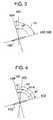
- the liquid crystal alignment directionis observed from the substrate normal direction, it is as shown in FIG. 3 .
- This diagramis a plan view of the transmissive display unit when seen from the normal direction on the side of the first substrate 31 after the first substrate 31 and the second substrate 32 are assembled.
- Reference numeral 101denotes an azimuth of the signal line 22 and it is drawn in parallel with FIG. 1 .
- a transmissive axis 104 of the first polarization film 41perpendicularly crosses a transmissive axis 106 of the second polarization film 42 .
- the transmissive axis 106is parallel with a liquid crystal alignment direction 102 . Since such a construction is similar to that of the transmissive IPS system, with respect to the transmissive display, a wide viewing angle which can also endure the application to the monitor is obtained in a manner similar to the transmissive IPS system.
- FIG. 4shows a correlation among a slow axis of the inner retardation layer 38 , the liquid crystal alignment direction, and a transmissive axis angle of the first polarization film.
- a slow axis direction 103 of the inner retardation layer 38is inclined by 67.5° from the liquid crystal alignment direction 102 and the transmissive axis 104 of the first polarization film is inclined by 90° from the liquid crystal alignment direction 102 .
- the laminate of the liquid crystal layer 10 , the inner retardation layer 38 , and the first polarization film 41becomes a circular polarization layer of a wide band.
- the incident lightbecomes circularly polarized light or enters a polarizing state similar to it and enters the reflection layer in almost the whole region of a visible wavelength.
- their electric vectorsbecome linearly polarized light which is parallel with an absorption axis of the first polarization film, so that the achromatic dark display is obtained.
- the expression (1) to decide the slow axis azimuth of the inner retardation layer 38 , the retardation of the inner retardation layer 38 , and the retardation of the liquid crystal layer 10are derived as follows by using a Poincare' sphere display.
- the Poincare' sphere displayis defined in the space in which stokes parameters (S1, S2, S3) describing the polarizing state are set to three axes.
- S1, S2, S3stokes parameters
- Each point on the Poincare' spherecorresponds to the polarizing state in a one-to-one relational manner.
- an intersection line (equator) with an (S1, S2) plane on the Poincare' spherecorresponds to the linearly polarized light.
- S1, S2, S3are expressed by the following expressions (2), (3), and (4) by using an arbitrary X-axial component Ex and an arbitrary Y-axial component Ey of an electric vector and a phase difference ⁇ between Ex and Ey, respectively.
- S 1( Ex 2 ⁇ Ey 2 )/( Ex 2 +Ey 2 ) (2)
- S 22 ExEy cos ⁇ /( Ex 2 +Ey 2 ) (3)
- S 32 ExEy sin ⁇ /( Ex 2 +y 2 ) (4)
- a conversion of the polarizing state by the retardation film or the liquid crystal layer 10 without a twistis expressed as a rotation around a line which is included in the (S1, S2) plane on the Poincare' sphere and passes through the center of the Poincare' sphere.
- a rotational angle at this timeis equal to 1 ⁇ 2 rotation if the retardation of the retardation film is equal to the half wave and to 1 ⁇ 4 rotation if it is equal to the quarter wave.
- the incident light of a representative wavelength in the visible light regionfor example, a wavelength of 550 nm at which human luminosity is the highest sequentially passes through the first polarization film 41 , the inner retardation layer 38 , and the liquid crystal layer 10 of the reflective display unit and reaches the pixel electrode 28 or the common electrode 29 .
- the crossing points with the S3-axisare called North Pole and South Pole, and the intersection line with the (S1, S2) plane is called an equator, as shown in FIG. 5
- incident light L 1 converted into linearly polarized light by the first polarization film 41is located on the equator on the Poincare' sphere.
- itis rotated by 1 ⁇ 2 rotation around a rotation axis, as a rotational center, whose azimuth is equal to ⁇ ′ PH by the inner retardation layer 38 , moved to another point L 2 on the equator, and converted into linearly polarized light having a different electric vector.
- the lightis rotated by 1 ⁇ 4 rotation around a rotation axis, as a rotational center, whose azimuth is equal to ⁇ ′ LC by the liquid crystal layer 10 , moved to North Pole NP, and converted into circularly polarized light.
- the retardationhas wavelength dependency.
- the light of a wavelength other than 550 nmis not rotated by 1 ⁇ 2 rotation but moved to a point out of the equator. Since the retardation of the blue light on the short wavelength side is larger than the half wave, as shown in FIG. 6 , the blue light is rotated by an angle larger than 1 ⁇ 2 rotation and moved to a position out of the equator.
- the retardation of the red light on the long wavelength sideis smaller than the half wave, as shown in FIG. 7 , the red light is rotated by an angle smaller than 1 ⁇ 2 rotation and moved to a position out of the equator.
- the red light on the long wavelength sideis rotated by the angle smaller than 1 ⁇ 4 rotation even in the liquid crystal layer 10 , since its movement is started from the Northern Hemisphere, the light reaches a position just on the North Pole by rotating the light by the angle smaller than 1 ⁇ 4 rotation.
- the light of each wavelengthis concentrated on a position near the North Pole and becomes almost the same circularly polarized light.
- the achromatic dark displaywhose reflective ratio is reduced in a wide region of the visible wavelength is obtained.
- FIG. 8Aobtained by seeing FIG. 5 from the S3-axis direction is used to clarify the relation between ⁇ ′ PH and ⁇ ′ LC .
- an auxiliary line(alternate long and short dash line) drawn so as to extend the 1 ⁇ 4 rotating direction is newly added. Since the auxiliary line is a prolonged line in the 1 ⁇ 4 rotating direction, it perpendicularly crosses the liquid crystal alignment direction (azimuth ⁇ ′ LC ) indicative of the center of the rotation.
- the slow axis direction (azimuth ⁇ ′ PH ) of the inner retardation layer indicative of the center of the 1 ⁇ 2 rotationdivides an angle between the S1-axis and the auxiliary line into two equal angles.
- FIG. 8C or 8 DAs another method of concentrating the incident light of each wavelength on the North Pole NP or the South Pole SP, there is a method shown in FIG. 8C or 8 D.
- the layout of the polarization films in the transmissive display unitis set to be similar to that of the tansmissive IPS system.
- ⁇ LC90°.
- the transflective liquid crystal display manufactured as mentioned aboveis connected to a driving apparatus, a backlight is arranged on the rear side of display, and the display state is observed.
- a display image according to the reflective displaycan be confirmed.
- a display image according to the transmissive displaycan be confirmed. Even if the observing direction from the normal of the substrate is changed in a wide range, gradation inversion does not occur and a reduction in contrast ratio is small.
- FIG. 10shows polar angle dependency of the dark display transmissive ratio. Values measured at different azimuths are also shown. The dark display transmissive ratio decreases sufficiently at any azimuth.
- polar angle dependency of the dark display transmissive ratio of the transmissive IPSis shown in FIG. 24 .
- transmissive display performance similar to that of the transmissive IPSis obtained.
- the conventional transflective liquid crystal displayin which the retardation films are arranged on the whole outside surfaces of the first and second substrates without using the inner retardation layer is manufactured. Its cross section is shown in FIG. 25 .
- a step forming layer 47having the same thickness as that of the inner retardation layer and having no retardation is arranged in place of the inner retardation layer.
- a first outside retardation film 44 of the same retardation and slow axis direction as those of the inner retardation layeris arranged between the first substrate 31 and the first polarization film 41 .
- a second outside retardation film 45 and a third outside retardation film 46are arranged between the second substrate 32 and the second polarization film 42 in order near the second substrate 32 .
- a retardation of the second outside retardation film 45is equal to that of the liquid crystal layer and its slow axis direction perpendicularly crosses the alignment direction of the liquid crystal layer 10 .
- a retardation of the third outside retardation film 46is equal to that of the first outside retardation film 44 and its slow axis direction perpendicularly crosses the first outside retardation film 44 .
- each of the first outside retardation film 44 , the second outside retardation film 45 , and the third outside retardation film 46a film made of a cycloolefin organic polymer in which the wavelength dependency of the retardation is relatively small is used.
- a construction of the reflective display unitis similar to that of the transflective liquid crystal display of the invention except for a point that the first outside retardation film 44 is used in place of the inner retardation layer.
- a construction of the transmissive display unitextremely differs from that of the transflective liquid crystal display of the invention. This is because the first outside retardation film 44 is also distributed to the transmissive display unit. Thus, in the normal direction, the third outside retardation film 46 which compensates the phase difference of the first outside retardation film 44 is necessary. Further, the second outside retardation film 45 which compensates the phase difference of the liquid crystal layer 10 is necessary.
- FIG. 26shows that the dark display transmissive ratio rapidly increases with an increase in polar angle in dependence on the azimuth and the contrast ratio decreases in dependence on the oblique direction. As will be obviously understood in comparison with FIG. 10 that the viewing angle performance is extremely inferior to that of the transflective liquid crystal display of the invention.
- the first outside retardation film 44 , the second outside retardation film 45 , and the third outside retardation film 46are arranged in the transmissive display unit, and even if the azimuths of the slow axis and the retardation are determined so as to compensate the phase difference of those laminates in the normal direction, the phase difference is not compensated in dependence on the oblique direction.
- both the reflective display in the light place and the transmissive display of the wide viewing angle similar to that of the transmissive liquid crystal displaycan be realized.
- the liquid crystal layer thickness dependency of the dark display transmissive ratiois compared with the conventional transflective liquid crystal display in which the retardation films are arranged on the whole outside surfaces of the first and second substrates.
- the conventional transflective liquid crystal displaysince the light entering the liquid crystal layer is the elliptically polarized light, the phase difference is applied by the liquid crystal layer and, if the phase difference changes in association with a fluctuation in liquid crystal layer thickness, the dark display transmissive ratio fluctuates largely.
- the liquid crystal layer thickness dependency of the dark display transmissive ratiois shown in FIG. 27 .
- the dark display transmissive ratioeasily increases and the contrast ratio decreases.
- the contrast ratiois not constant in the display screen but is observed as a variation in dark display and an unwell feeling is applied to the user.
- the transmissive display unitsince the light entering the liquid crystal layer is the linearly polarized light and its electric vector is parallel with the alignment direction of the liquid crystal layer. Since only either the normal light beam or the abnormal light beam occurs in the liquid crystal layer, the phase difference cannot be applied by the liquid crystal layer. Therefore, as shown in FIG. 11 , even if the liquid crystal layer thickness fluctuates, the dark display transmissive ratio hardly fluctuates. There is such a feature that the contrast ratio is difficult to decrease and even if the liquid crystal layer thickness fluctuates in the display screen, a variation in dark display is difficult to occur. As mentioned above, according to the liquid crystal display of the invention, in addition to the transmissive display of the wide viewing angle, the uniform display without a variation in dark display can be obtained.
- liquid crystal displayIn the case of applying the liquid crystal display to a cellular phone or the like, a thin size and a light weight are required. Attention is paid to the thickness of liquid crystal panel and the liquid crystal display of the invention is compared with the conventional transflective liquid crystal display in which the retardation films are arranged on the whole outside surfaces of the first and second substrates.
- the liquid crystal panelindicates a portion sandwiched between the first polarization film and the second polarization film.
- a thickness of each of the first and second substratesis equal to 0.5 mm
- a thickness of each of the first and second polarization filmsis equal to 0.12 mm
- a thickness of each of the first, second, and third retardation filmsis equal to 0.05 mm.
- the thickness of liquid crystal panelis substantially determined by those component elements. Since a thickness of each of the color filter, inner retardation layer, and the like formed on the first substrate and a thickness of each of the thin film transistors, various lines, insulation films, and the like formed on the second substrate are equal to a few ⁇ m, they hardly exert an influence on the thickness of liquid crystal panel.
- the thickness of liquid crystal panelis equal to 1.39 mm.
- the liquid crystal display of the inventionis characterized in that the thickness of liquid crystal panel is equal to 1.24 mm and thin.
- FIG. 12A cross sectional view of the liquid crystal display of the embodiment is shown in FIG. 12 .
- the inner retardation layer 38is formed between the third alignment layer 35 and the color filter 36 .
- the color filter 36 , the leveling layer 37 , and the first alignment layer 33exist between the inner retardation layer 38 and the liquid crystal layer 10 .
- the non-reacted photoreactive liquid crystal and the initiatorremain in the inner retardation layer 38 . If they are mixed into the liquid crystal layer 10 , there is a case where performance such as a holding ratio or the like deteriorates.
- the color filter 36is manufactured. At this time, although it is necessary to position the inner retardation layer 38 and the color filter 36 , since the inner retardation layer 38 itself is transparent, it cannot be used as an index for the positioning. If a positioning index is preliminarily formed in an opaque layer before manufacturing the inner retardation layer 38 , and the inner retardation layer 38 and the color filter 36 are patterned by using such an index as a reference, the inner retardation layer 38 and the color filter 36 can be positioned.
- the inclining direction of the slits 30 of the pixel electrode 28is set to two kinds.
- a plan view of one pixel of the transflective liquid crystal display of the embodimentis shown in FIG. 13 .
- the slits 30are inclined by ⁇ 75° and 75° from the signal line 22 , respectively.
- the liquid crystal alignment direction 102 , the slow axis direction 103 of the inner retardation layer 38 , the transmissive axis 104 of the first polarization film 41 , and the transmissive axis 106 of the second polarization film 42are changed.
- the liquid crystal alignment direction 102is set to be perpendicular to the signal line direction 101 .
- An angle between the liquid crystal alignment direction 102 and the electric field direction in the upper half portion of the pixel and that in the lower half portionare set to the same angle of 75°.
- the slow axis direction 103 of the inner retardation layer, the transmissive axis 104 of the first polarization film, and the transmissive axis 106 of the second polarization filmare set so as to be rotated by 15° clockwise with respect to the disclosure of FIGS. 4 and 5 in such a manner that the relative angle relation with respect to the liquid crystal alignment direction 102 is equalized to that of the embodiment 1.
- the common line 23is arranged so as to transverse the pixel in the center portion.
- the portion where the slits 30 are inclined by ⁇ 75° from the signal line 22 and the portion where they are inclined by 75° from the signal line 22are distributed so as to have the same area in both the reflective display unit and the transmissive display unit.
- the liquid crystal alignmentdoes not change. Since this center portion always has the same liquid crystal alignment as that of the dark display, it is observed as a dark line and the reflective ratio or transmissive ratio of one pixel decreases. However, since the slits 30 are arranged so that their inclining direction changes with respect to the upper half portion and the lower half portion of the pixel, the dark line portion is distributed in the shorter side direction, thereby minimizing the decrease in the reflective ratio or the transmissive ratio.
- the liquid crystal layer alignment direction when the voltage is appliedis set to the two directions.
- the azimuth dependency of the viewing angle performance in the right half portion and that in the left half portionare set off, so that an effect of further improving the viewing angle performance can be obtained.
- each slit 30is set into a V-character shape and the director distribution of the liquid crystal layer when the voltage is applied is set to the two directions.
- the liquid crystal alignment direction, the slow axis direction of the inner retardation layer, and the transmissive axis of the first polarization film, and the transmissive axis of the second polarization filmare set to those similar to the embodiment 3.
- the portion where the slits 30 are inclined by ⁇ 75° from the signal line 22 and the portion where they are inclined by 75° from the signal line 22can be distributed so as to have the same area in both the reflective display unit and the transmissive display unit. Also in this case, the effect of improving the viewing angle performance can be obtained.
- the dark lineappears in parallel with the long side of the pixel, it is relatively long and the decrease in the reflective ratio or the transmissive ratio is relatively large.
- the third alignment layer 35has a function to decide the slow axis azimuth of the inner retardation layer 38 .
- a light alignment layer to decide the alignment direction by the light irradiationis used as a third alignment layer 35 .
- a light alignment layerthere is a layer using a photo dimerization reaction of a cinnamic acid or coumarin or a layer using a photo cleavage reaction of a polymer.
- the light alignment layeris not spread as compared with the alignment layer according to the conventional rubbing method.
- a cause in which a tilt angle which is applied to the liquid crystal layer is small and the alignment change of the liquid crystal layer when the voltage is applied is unstablecan be mentioned. Since the inner retardation layer does not need the tilt angle, fundamentally, any kind of light alignment layer can be applied to the third alignment layer 35 . In this case, the number of times of the rubbing process which is executed to the first substrate 31 can be set to one time.
- FIG. 17A plan view of a liquid crystal display of the embodiment is shown in FIG. 17 .
- both the pixel electrode 28 and the common electrode 29are set into a comb-toothed shape and formed in the same layer.
- an arch-shaped electric fieldis formed between the pixel electrode 28 and the common electrode 29 and the liquid crystal layer is driven.
- the electric field directionis perpendicular to the signal line 22 .
- the slow axis direction 103 of the inner retardation layer 38the transmissive axis direction 104 of the first polarization film 41 , and the transmissive axis direction 106 of the second polarization film 42 are changed.
- FIGS. 18 and 19show the reflective display unit and transmissive display unit, respectively.
- the liquid crystal alignment direction 102is set to 15° from the azimuth 101 of the signal line 22 so as to be set to 75° from the electric field direction. This setting corresponds to that the layout is rotated counterclockwise by 90° from the layout of the embodiment 1.
- the slow axis direction 103 of the inner retardation layer, the transmissive axis 104 of the first polarization film, and the transmissive axis 106 of the second polarization filmare set so as to be rotated counterclockwise by 90° from those shown in FIGS. 4 and 3 in such a manner that the relative angle relation for the liquid crystal alignment direction 102 is substantially the same as that in the embodiment 1.
- both the reflective display at a light place and the transmissive display of the wide viewing angle similar to that of the transmissive liquid crystal displaycan be realized. Since the pixel electrode 28 and the common electrode 29 are formed in the same layer, the manufacturing steps can be simplified.
- FIG. 20A plan view of a liquid crystal display of the embodiment is shown in FIG. 20 .
- the pixel electrode 28 and the common electrode 29are formed in the same layer in a manner similar to the embodiment 5. Further the comb-toothed structure is set into a V-character shape.
- the direction of the electric field which is formed between the pixel electrode 28 and the common electrode 29 when the voltage is appliedis set to two directions.
- the slow axis direction 103 of the inner retardation layer 38 , the transmissive axis 104 of the first polarization film 41 , and the transmissive axis 106 of the second polarization film 42are changed.
- FIGS. 21 and 22show the reflective display unit and transmissive display unit, respectively.
- the liquid crystal alignment direction 102is set in parallel with the azimuth 101 of the signal line 22 so as to be set to 75° from the electric field direction. This setting corresponds to that the layout is rotated counterclockwise by 75° from the layout of the embodiment 1.
- the slow axis direction 103 of the inner retardation layer, the transmissive axis 104 of the first polarization film, and the transmissive axis 106 of the second polarization filmare set so as to be rotated counterclockwise by 75° as compared with the layout shown in FIGS. 4 and 3 in such a manner that the relative angle relation for the liquid crystal alignment direction 102 is substantially the same as that in the embodiment 1.
- the liquid crystal layer alignment direction when the voltage is appliedis set to the two directions.
- the azimuth dependency of the viewing angle performance in the right half portion and that in the left half portionare set off, so that the effect of further improving the viewing angle performance can be obtained.
- FIG. 23A cross sectional view of a liquid crystal display of the embodiment is shown in FIG. 23 .
- the step forming layer 47having the same thickness as that of the inner retardation layer 38 and having no retardation is arranged in place of the inner retardation layer 38 in the construction of the embodiment 1.
- the thicknesses of those substratesare reduced to 30 ⁇ m, respectively.
- a mechanical polishing methodhas been used to reduce the thicknesses of the first substrate 31 and the second substrate 32 , for example, another method of using corrosion by an acid such as a hydrofluoric acid or the like can be used.
- the inner retardation layer 38is formed at the position corresponding to the reflective display unit.
- a first holding layer 54is formed outside of the first substrate 31 and a second holding layer 55 is formed outside of the second substrate 32 , respectively.
- Each of the first holding layer 54 and the second holding layer 55is made of a transparent resin. Since their thicknesses are reduced, the first and second holding layers have a function of reinforcing the first substrate 31 and second substrate 32 in which a strength has been weakened.
- the first holding layer 54has a function of flattening the rough surface caused by the inner retardation layer 38 . If isotropic media whose retardation is equal to zero are used for the first holding layer 54 and the second holding layer 55 , since no influence is exercised on the polarizing state of the transmissive light, the transmissive display of the wide viewing angle can be obtained in a manner similar to the embodiment 1. Since the first holding layer 54 and the second holding layer 55 are made of the transparent resin and are lighter than the first substrate 31 and second substrate 32 made of glass, an effect of reducing a weight of the whole liquid crystal display can be obtained.
Landscapes
- Physics & Mathematics (AREA)
- Nonlinear Science (AREA)
- Mathematical Physics (AREA)
- Chemical & Material Sciences (AREA)
- Crystallography & Structural Chemistry (AREA)
- General Physics & Mathematics (AREA)
- Optics & Photonics (AREA)
- Liquid Crystal (AREA)
- Polarising Elements (AREA)
Abstract
Description
2θPH=±45°+θLC (1)
where, θLChas to be set to either 0° or ±90° since the layout of the polarization films in the transmissive display unit is similar to that of the transmissive IPS. Thus, θPHis equal to ±22.5° (a range from 20° or more to 25° or less in consideration of an allowance of ±10% in manufacturing) or ±67.5° (a range from 60° or more to 75° or less in consideration of an allowance of ±10% in manufacturing). By arranging the laminate of the liquid crystal layer and the inner retardation layer like a quarter wave plate of the wide band, a reflective ratio of the whole visible wavelength region decreases and an achromatic reflection display of the small reflective ratio is obtained.
S1=(Ex2−Ey2)/(Ex2+Ey2) (2)
S2=2ExEycos δ/(Ex2+Ey2) (3)
S3=2ExEysin δ/(Ex2+y2) (4)
2θ′PH=90°+θ′LC (5)
2θ′PH=−90°+θ′LC (6)
Claims (7)
Priority Applications (1)
| Application Number | Priority Date | Filing Date | Title |
|---|---|---|---|
| US11/397,087US7688406B2 (en) | 2004-05-25 | 2006-04-04 | Liquid crystal display apparatus |
Applications Claiming Priority (2)
| Application Number | Priority Date | Filing Date | Title |
|---|---|---|---|
| JP2004154691AJP4223992B2 (en) | 2004-05-25 | 2004-05-25 | Liquid crystal display |
| JP2004-154691 | 2004-05-25 |
Related Child Applications (1)
| Application Number | Title | Priority Date | Filing Date |
|---|---|---|---|
| US11/397,087ContinuationUS7688406B2 (en) | 2004-05-25 | 2006-04-04 | Liquid crystal display apparatus |
Publications (2)
| Publication Number | Publication Date |
|---|---|
| US20050264731A1 US20050264731A1 (en) | 2005-12-01 |
| US7088409B2true US7088409B2 (en) | 2006-08-08 |
Family
ID=35424781
Family Applications (2)
| Application Number | Title | Priority Date | Filing Date |
|---|---|---|---|
| US11/135,828Expired - Fee RelatedUS7088409B2 (en) | 2004-05-25 | 2005-05-23 | Liquid crystal display apparatus |
| US11/397,087Expired - Fee RelatedUS7688406B2 (en) | 2004-05-25 | 2006-04-04 | Liquid crystal display apparatus |
Family Applications After (1)
| Application Number | Title | Priority Date | Filing Date |
|---|---|---|---|
| US11/397,087Expired - Fee RelatedUS7688406B2 (en) | 2004-05-25 | 2006-04-04 | Liquid crystal display apparatus |
Country Status (2)
| Country | Link |
|---|---|
| US (2) | US7088409B2 (en) |
| JP (1) | JP4223992B2 (en) |
Cited By (43)
| Publication number | Priority date | Publication date | Assignee | Title |
|---|---|---|---|---|
| US20060050218A1 (en)* | 2004-09-09 | 2006-03-09 | Baek Heume I | In-plane switching mode liquid crystal display device |
| US20060125984A1 (en)* | 2004-12-13 | 2006-06-15 | Samsung Electronics Co., Ltd. | Display device and thin film transistor array panel for display device and manufacturing method thereof |
| US20060170846A1 (en)* | 2005-02-03 | 2006-08-03 | Seiko Epson Corporation | Liquid crystal display and electronic apparatus |
| US20060279677A1 (en)* | 2005-06-09 | 2006-12-14 | Sanyo Epson Imaging Devices Corporation | Liquid crystal device and electronic apparatus |
| US20070013773A1 (en)* | 2005-07-15 | 2007-01-18 | Sanyo Epson Imaging Devices Corp. | Liquid crystal display device and electronic apparatus |
| US20070046869A1 (en)* | 2005-08-23 | 2007-03-01 | Au Optronics Corporation | Liquid crystal display and method for manufacturing the same |
| US20070076146A1 (en)* | 2005-09-30 | 2007-04-05 | Sanyo Epson Imaging Devices Corporation | Liquid crystal device and electronic apparatus |
| US20070103626A1 (en)* | 2005-11-07 | 2007-05-10 | Masateru Morimoto | Transflective liquid crystal display device |
| US20070126969A1 (en)* | 2005-12-05 | 2007-06-07 | Semiconductor Energy Laboratory Co., Ltd. | Liquid crystal display device |
| US20070126968A1 (en)* | 2005-10-18 | 2007-06-07 | Semiconductor Energy Laboratory Co., Ltd. | Liquid crystal display device |
| US20070146591A1 (en)* | 2005-12-05 | 2007-06-28 | Semiconductor Energy Laboratory Co., Ltd. | Liquid crystal display device |
| US20070182892A1 (en)* | 2006-02-07 | 2007-08-09 | Sanyo Epson Imaging Devices Corporation | Liquid crystal display device, methods for manufacturing the same, and electronic apparatus |
| US20070236640A1 (en)* | 2006-04-06 | 2007-10-11 | Semiconductor Energy Laboratory Co., Ltd. | Liquid crystal display device, semiconductor device, and electronic appliance |
| US20070263148A1 (en)* | 2006-05-15 | 2007-11-15 | Masahiro Teramoto | Liquid Crystal Display Device |
| US20070284627A1 (en)* | 2006-05-16 | 2007-12-13 | Semiconductor Energy Laboratory Co., Ltd. | Liquid crystal display device and semiconductor device |
| US20080068543A1 (en)* | 2006-09-19 | 2008-03-20 | Epson Imaging Devices Corporation | Liquid crystal display device |
| US20080074588A1 (en)* | 2006-09-22 | 2008-03-27 | Shinji Sekiguchi | Liquid crystal display device and manufacturing method thereof |
| US20080094554A1 (en)* | 2006-10-20 | 2008-04-24 | Hitachi Displays, Ltd. | Liquid crystal display unit |
| US20080136990A1 (en)* | 2006-10-31 | 2008-06-12 | Semiconductor Energy Laboratory Co., Ltd. | Liquid crystal display device and electronic device |
| US20080180613A1 (en)* | 2007-01-25 | 2008-07-31 | Seiko Epson Corporation | Liquid crystal display, method for producing liquid crystal display, and electronic apparatus |
| US20080180616A1 (en)* | 2007-01-26 | 2008-07-31 | Hitachi Displays, Ltd. | Transflective Liquid Crystal Display Device |
| US20080180622A1 (en)* | 2007-01-25 | 2008-07-31 | Epson Imaging Devices Corporation | Liquid crystal display device and method of manufacturing the same |
| US20080186420A1 (en)* | 2007-02-06 | 2008-08-07 | Sony Corporation | Liquid crystal display device and electronic apparatus including the same |
| US20080239220A1 (en)* | 2007-03-28 | 2008-10-02 | Epson Imaging Devices Corporation | Liquid crystal display device and electronic apparatus |
| US20080273149A1 (en)* | 2007-05-04 | 2008-11-06 | Au Optronics Corporation | Optical compensation film, fabricating method of the optical compensation film and liquid crystal display panel using the same |
| US20080291377A1 (en)* | 2007-04-26 | 2008-11-27 | Shinji Sekiguchi | Liquid Crystal Display Device and Manufacturing Method Thereof |
| US20090015774A1 (en)* | 2007-07-13 | 2009-01-15 | Hitachi Displays, Ltd. | Liquid Crystal Display Device |
| US20090021675A1 (en)* | 2007-07-19 | 2009-01-22 | Atsushi Kishioka | Liquid Crystal Display Device, Manufacturing Method Thereof, and Color Filter Substrate |
| US20090135118A1 (en)* | 2007-11-28 | 2009-05-28 | Sony Corporation | Liquid crystal display device |
| US20090262287A1 (en)* | 2006-08-02 | 2009-10-22 | Kenji Nishida | Display device |
| US20090279027A1 (en)* | 2006-07-07 | 2009-11-12 | Kenji Nishida | Display device |
| US20090279029A1 (en)* | 2008-05-08 | 2009-11-12 | Sony Corporation | Liquid crystal display |
| US20100044337A1 (en)* | 2007-01-25 | 2010-02-25 | Tokyo Seikan Kaisha | Container for inspection |
| US20100134733A1 (en)* | 2007-08-09 | 2010-06-03 | Hisashi Watanabe | Liquid crystal display unit |
| CN101211072B (en)* | 2006-12-25 | 2010-10-13 | 索尼株式会社 | Liquid crystal display device and display apparatus |
| US8089590B2 (en) | 2007-08-06 | 2012-01-03 | Chimei Innolux Corporation | Transflective liquid crystal display |
| US8208102B2 (en) | 2006-07-21 | 2012-06-26 | Sharp Kabushiki Kaisha | Display device having reflective region and transmissive region |
| US8274628B2 (en) | 2004-12-06 | 2012-09-25 | Semiconductor Energy Laboratory Co., Ltd. | Liquid crystal display device |
| USRE43694E1 (en) | 2000-04-28 | 2012-10-02 | Sharp Kabushiki Kaisha | Stamping tool, casting mold and methods for structuring a surface of a work piece |
| CN101441371B (en)* | 2007-11-19 | 2013-08-21 | 株式会社日本显示器西 | Liquid crystal device and electronic apparatus |
| US8537318B2 (en) | 2006-06-02 | 2013-09-17 | Semiconductor Energy Laboratory Co., Ltd. | Liquid crystal display device and electronic appliance |
| US20180284332A1 (en)* | 2014-11-20 | 2018-10-04 | Nitto Denko Corporation | Circular polarization plate for organic el display device and organic el display device |
| US11967598B2 (en) | 2006-09-29 | 2024-04-23 | Semiconductor Energy Laboratory Co., Ltd. | Display device |
Families Citing this family (76)
| Publication number | Priority date | Publication date | Assignee | Title |
|---|---|---|---|---|
| JP4496874B2 (en)* | 2004-07-29 | 2010-07-07 | Nec液晶テクノロジー株式会社 | Transflective liquid crystal display device and electronic device equipped with the same |
| JP4687870B2 (en)* | 2004-09-02 | 2011-05-25 | ソニー株式会社 | Liquid crystal display device and manufacturing method thereof |
| KR101217945B1 (en)* | 2004-11-12 | 2013-01-02 | 메르크 파텐트 게엠베하 | Transflective ips liquid crystal display |
| JP4816862B2 (en)* | 2004-12-16 | 2011-11-16 | ソニー株式会社 | Liquid crystal display |
| DE102006057333B4 (en)* | 2005-12-30 | 2010-01-28 | Lg Display Co., Ltd. | IPS liquid crystal display device |
| KR100760942B1 (en)* | 2005-12-30 | 2007-09-21 | 엘지.필립스 엘시디 주식회사 | In-plane Switching Mode Liquid Crystal Display Device |
| JP4883521B2 (en) | 2006-03-07 | 2012-02-22 | Nltテクノロジー株式会社 | Transflective liquid crystal display device |
| JP4238877B2 (en) | 2006-03-28 | 2009-03-18 | エプソンイメージングデバイス株式会社 | FFS mode LCD panel |
| JP4788453B2 (en)* | 2006-04-11 | 2011-10-05 | ソニー株式会社 | Liquid crystal device, manufacturing method thereof, and electronic apparatus |
| JP4884829B2 (en)* | 2006-05-10 | 2012-02-29 | 株式会社 日立ディスプレイズ | Liquid crystal display |
| US8106865B2 (en)* | 2006-06-02 | 2012-01-31 | Semiconductor Energy Laboratory Co., Ltd. | Display device and driving method thereof |
| CN101479656B (en)* | 2006-06-26 | 2012-01-11 | 夏普株式会社 | display device |
| KR101254064B1 (en)* | 2006-06-30 | 2013-04-12 | 엘지디스플레이 주식회사 | In plane electrode mode Transflective LCD |
| JP4907245B2 (en)* | 2006-07-07 | 2012-03-28 | 株式会社 日立ディスプレイズ | Transflective liquid crystal display device |
| JP4837482B2 (en) | 2006-08-03 | 2011-12-14 | 株式会社 日立ディスプレイズ | Transflective liquid crystal display device |
| JP2008065197A (en)* | 2006-09-11 | 2008-03-21 | Hitachi Displays Ltd | Liquid crystal display device and method for manufacturing the same |
| TW200815859A (en) | 2006-09-19 | 2008-04-01 | Epson Imaging Devices Corp | Liquid crystal display device |
| JP2008076849A (en)* | 2006-09-22 | 2008-04-03 | Hitachi Displays Ltd | Liquid crystal display device and manufacturing method thereof |
| JP5150182B2 (en)* | 2006-09-22 | 2013-02-20 | 株式会社ジャパンディスプレイイースト | Manufacturing method of liquid crystal display device |
| JP4886474B2 (en)* | 2006-11-06 | 2012-02-29 | 株式会社 日立ディスプレイズ | Liquid crystal display |
| JP2008145525A (en)* | 2006-12-06 | 2008-06-26 | Seiko Epson Corp | Liquid crystal device and electronic device |
| JP4814776B2 (en)* | 2006-12-14 | 2011-11-16 | 株式会社 日立ディスプレイズ | Transflective liquid crystal display device |
| JP4962008B2 (en)* | 2007-01-06 | 2012-06-27 | ソニー株式会社 | Liquid crystal device and electronic device |
| JP2008170497A (en)* | 2007-01-09 | 2008-07-24 | Hitachi Displays Ltd | Liquid crystal display device and manufacturing method thereof |
| JP2008170501A (en)* | 2007-01-09 | 2008-07-24 | Hitachi Displays Ltd | Liquid crystal display device and manufacturing method thereof |
| JP5013367B2 (en) | 2007-01-17 | 2012-08-29 | Nltテクノロジー株式会社 | Liquid crystal display device and method of manufacturing liquid crystal display device |
| TWI308307B (en)* | 2007-01-18 | 2009-04-01 | Tpo Displays Corp | Image display system |
| JP4462280B2 (en) | 2007-02-22 | 2010-05-12 | エプソンイメージングデバイス株式会社 | Liquid crystal device and electronic device |
| US7839472B2 (en) | 2007-02-23 | 2010-11-23 | Sony Corporation | Liquid crystal device and electronic apparatus |
| JP4529984B2 (en) | 2007-02-26 | 2010-08-25 | エプソンイメージングデバイス株式会社 | Liquid crystal device and electronic device |
| JP2008209852A (en)* | 2007-02-28 | 2008-09-11 | Epson Imaging Devices Corp | Liquid crystal device and electronic device |
| JP4337893B2 (en) | 2007-03-12 | 2009-09-30 | エプソンイメージングデバイス株式会社 | Liquid crystal device and electronic device |
| US7880842B2 (en)* | 2007-03-20 | 2011-02-01 | Fujifilm Corporation | Liquid-crystal display device having liquid crystal cell with plural domains |
| JP5057324B2 (en) | 2007-04-19 | 2012-10-24 | 株式会社ジャパンディスプレイウェスト | Liquid crystal device and electronic device |
| JP2008275966A (en) | 2007-05-01 | 2008-11-13 | Epson Imaging Devices Corp | Liquid crystal display device and electronic equipment |
| US7746433B2 (en) | 2007-05-01 | 2010-06-29 | Epson Imaging Devices Corporation | Liquid crystal display and electronic apparatus |
| JP5067690B2 (en)* | 2007-05-18 | 2012-11-07 | Nltテクノロジー株式会社 | Liquid crystal display device and terminal device |
| JP5013370B2 (en) | 2007-05-18 | 2012-08-29 | Nltテクノロジー株式会社 | Liquid crystal display device and terminal device |
| CN101669065B (en)* | 2007-06-14 | 2011-12-28 | 夏普株式会社 | Liquid crystal display panel and liquid crystal display device |
| JP4900072B2 (en) | 2007-06-14 | 2012-03-21 | ソニー株式会社 | Liquid crystal device and electronic device |
| JP5305190B2 (en) | 2007-06-21 | 2013-10-02 | 株式会社ジャパンディスプレイ | Liquid crystal display |
| JP5026162B2 (en) | 2007-06-21 | 2012-09-12 | 株式会社ジャパンディスプレイイースト | Liquid crystal display |
| US8081178B2 (en) | 2007-07-10 | 2011-12-20 | Sony Corporation | Electro-optical device, driving circuit, and electronic apparatus |
| JP4960164B2 (en)* | 2007-07-20 | 2012-06-27 | 株式会社ジャパンディスプレイイースト | Liquid crystal display |
| JP2009047841A (en)* | 2007-08-17 | 2009-03-05 | Hitachi Displays Ltd | Liquid crystal display |
| JP5472773B2 (en)* | 2007-08-30 | 2014-04-16 | Nltテクノロジー株式会社 | Transflective liquid crystal display device |
| JP5429584B2 (en) | 2007-09-26 | 2014-02-26 | Nltテクノロジー株式会社 | Display device, portable device using the same, and terminal device |
| JP5171189B2 (en)* | 2007-09-28 | 2013-03-27 | 株式会社ジャパンディスプレイウェスト | Liquid crystal display device, method for manufacturing liquid crystal display device, and electronic apparatus |
| JP5291913B2 (en)* | 2007-10-16 | 2013-09-18 | 株式会社ジャパンディスプレイウェスト | Manufacturing method of transflective liquid crystal display panel |
| JP2009103815A (en)* | 2007-10-22 | 2009-05-14 | Dainippon Printing Co Ltd | Transflective liquid crystal display device, phase modulation element, exposure method, and method of manufacturing phase modulation element |
| JP5151408B2 (en) | 2007-11-08 | 2013-02-27 | Nltテクノロジー株式会社 | Transflective liquid crystal display device |
| JP2009128860A (en) | 2007-11-28 | 2009-06-11 | Seiko Epson Corp | Liquid crystal device, method for manufacturing liquid crystal device, and electronic apparatus |
| US8390772B2 (en) | 2007-11-28 | 2013-03-05 | Sony Corporation | Liquid crystal display device |
| JP2009145745A (en)* | 2007-12-17 | 2009-07-02 | Hitachi Displays Ltd | Liquid crystal display device and manufacturing method thereof |
| CN101925853A (en)* | 2008-01-25 | 2010-12-22 | 夏普株式会社 | Liquid crystal display device |
| JP2009198703A (en)* | 2008-02-20 | 2009-09-03 | Sony Corp | Liquid crystal display device and method of manufacturing the same |
| JP5281810B2 (en)* | 2008-03-12 | 2013-09-04 | 株式会社ジャパンディスプレイウェスト | Liquid crystal device |
| JP2009237022A (en) | 2008-03-26 | 2009-10-15 | Seiko Epson Corp | Liquid crystal display device and electronic apparatus |
| JP2009258332A (en) | 2008-04-16 | 2009-11-05 | Seiko Epson Corp | Liquid crystal display device and electronic device |
| JP5211844B2 (en)* | 2008-05-16 | 2013-06-12 | Dic株式会社 | Patterned retardation film |
| JP5306718B2 (en)* | 2008-06-19 | 2013-10-02 | 株式会社ジャパンディスプレイウェスト | Liquid crystal display device and electronic device |
| JP4623215B2 (en)* | 2009-02-05 | 2011-02-02 | ソニー株式会社 | Liquid crystal device and electronic device |
| JP5397989B2 (en)* | 2009-03-12 | 2014-01-22 | 株式会社ジャパンディスプレイ | Liquid crystal display |
| JP5455011B2 (en)* | 2009-03-18 | 2014-03-26 | 株式会社ジャパンディスプレイ | LCD panel |
| JP5299777B2 (en) | 2009-07-01 | 2013-09-25 | Nltテクノロジー株式会社 | Transflective liquid crystal display device |
| JP5500712B2 (en)* | 2009-09-02 | 2014-05-21 | 株式会社ジャパンディスプレイ | LCD panel |
| JP4629152B2 (en)* | 2010-03-10 | 2011-02-09 | 株式会社 日立ディスプレイズ | Liquid crystal display device |
| JP4928646B2 (en)* | 2011-11-01 | 2012-05-09 | 三菱電機株式会社 | Liquid crystal display device and manufacturing method thereof |
| US9853164B2 (en)* | 2012-10-03 | 2017-12-26 | Sharp Kabushiki Kaisha | Semiconductor device and display device |
| JP6116220B2 (en)* | 2012-12-12 | 2017-04-19 | 三菱電機株式会社 | LCD panel |
| CN103811532B (en) | 2014-01-28 | 2016-07-06 | 京东方科技集团股份有限公司 | A kind of display device and preparation method thereof |
| JP5681822B2 (en)* | 2014-03-10 | 2015-03-11 | 株式会社ジャパンディスプレイ | LCD panel |
| CN104777649A (en)* | 2015-04-21 | 2015-07-15 | 合肥鑫晟光电科技有限公司 | Display substrate, manufacturing method for same and display device |
| WO2017170350A1 (en)* | 2016-03-30 | 2017-10-05 | シャープ株式会社 | Liquid crystal display device |
| CN106094366B (en)* | 2016-08-23 | 2019-02-01 | 深圳市华星光电技术有限公司 | The production method and IPS type array substrate of IPS type array substrate |
| JP2025025395A (en) | 2023-08-09 | 2025-02-21 | シャープディスプレイテクノロジー株式会社 | Transflective liquid crystal display device |
Citations (8)
| Publication number | Priority date | Publication date | Assignee | Title |
|---|---|---|---|---|
| JPH11242226A (en) | 1997-12-26 | 1999-09-07 | Sharp Corp | Liquid crystal display |
| US20010048496A1 (en)* | 2000-04-17 | 2001-12-06 | Heum-Il Baek | Transflective liquid crystal display device |
| US6583840B1 (en)* | 1999-05-26 | 2003-06-24 | Matsushita Electric Industrial Co., Ltd. | Liquid crystal display element with comb electrodes having reflective projections and producing method thereof |
| US6608660B1 (en)* | 1999-07-16 | 2003-08-19 | Seiko Epson Corporation | Liquid crystal display device including shading film with opening and reflector with opening in the opening in the shading film |
| US6611310B2 (en)* | 2001-03-07 | 2003-08-26 | Hitachi, Ltd. | Liquid crystal display device |
| JP2003279957A (en) | 2002-03-25 | 2003-10-02 | Seiko Epson Corp | Liquid crystal display device, manufacturing method thereof, and electronic device |
| WO2004015486A1 (en) | 2002-08-02 | 2004-02-19 | Koninklijke Philips Electronics N.V. | Transflective liquid crystal display device |
| US6914656B2 (en)* | 2002-05-24 | 2005-07-05 | Nec Corporation | Semi-transmissive liquid crystal display device |
Family Cites Families (1)
| Publication number | Priority date | Publication date | Assignee | Title |
|---|---|---|---|---|
| JP3873869B2 (en)* | 2002-02-26 | 2007-01-31 | ソニー株式会社 | Liquid crystal display device and manufacturing method thereof |
- 2004
- 2004-05-25JPJP2004154691Apatent/JP4223992B2/ennot_activeExpired - Fee Related
- 2005
- 2005-05-23USUS11/135,828patent/US7088409B2/ennot_activeExpired - Fee Related
- 2006
- 2006-04-04USUS11/397,087patent/US7688406B2/ennot_activeExpired - Fee Related
Patent Citations (9)
| Publication number | Priority date | Publication date | Assignee | Title |
|---|---|---|---|---|
| JPH11242226A (en) | 1997-12-26 | 1999-09-07 | Sharp Corp | Liquid crystal display |
| US20010052948A1 (en)* | 1997-12-26 | 2001-12-20 | Sharp Kabushiki Kaisha | Liquid crystal display |
| US6583840B1 (en)* | 1999-05-26 | 2003-06-24 | Matsushita Electric Industrial Co., Ltd. | Liquid crystal display element with comb electrodes having reflective projections and producing method thereof |
| US6608660B1 (en)* | 1999-07-16 | 2003-08-19 | Seiko Epson Corporation | Liquid crystal display device including shading film with opening and reflector with opening in the opening in the shading film |
| US20010048496A1 (en)* | 2000-04-17 | 2001-12-06 | Heum-Il Baek | Transflective liquid crystal display device |
| US6611310B2 (en)* | 2001-03-07 | 2003-08-26 | Hitachi, Ltd. | Liquid crystal display device |
| JP2003279957A (en) | 2002-03-25 | 2003-10-02 | Seiko Epson Corp | Liquid crystal display device, manufacturing method thereof, and electronic device |
| US6914656B2 (en)* | 2002-05-24 | 2005-07-05 | Nec Corporation | Semi-transmissive liquid crystal display device |
| WO2004015486A1 (en) | 2002-08-02 | 2004-02-19 | Koninklijke Philips Electronics N.V. | Transflective liquid crystal display device |
Cited By (150)
| Publication number | Priority date | Publication date | Assignee | Title |
|---|---|---|---|---|
| USRE46606E1 (en) | 2000-04-28 | 2017-11-14 | Sharp Kabushiki Kaisha | Stamping tool, casting mold and methods for structuring a surface of a work piece |
| USRE44830E1 (en) | 2000-04-28 | 2014-04-08 | Sharp Kabushiki Kaisha | Stamping tool, casting mold and methods for structuring a surface of a work piece |
| USRE43694E1 (en) | 2000-04-28 | 2012-10-02 | Sharp Kabushiki Kaisha | Stamping tool, casting mold and methods for structuring a surface of a work piece |
| US7630044B2 (en)* | 2004-09-09 | 2009-12-08 | Lg Display Co., Ltd. | In-plane switching mode LCD device having the interval between the common and pixel electrodes in the reflective part being greater than the interval between the common and pixel electrodes in transmitting part |
| US20060050218A1 (en)* | 2004-09-09 | 2006-03-09 | Baek Heume I | In-plane switching mode liquid crystal display device |
| US8593591B2 (en) | 2004-12-06 | 2013-11-26 | Semiconductor Energy Laboratory Co., Ltd. | Liquid crystal display device |
| US8274628B2 (en) | 2004-12-06 | 2012-09-25 | Semiconductor Energy Laboratory Co., Ltd. | Liquid crystal display device |
| US20060125984A1 (en)* | 2004-12-13 | 2006-06-15 | Samsung Electronics Co., Ltd. | Display device and thin film transistor array panel for display device and manufacturing method thereof |
| US7420635B2 (en)* | 2005-02-03 | 2008-09-02 | Seiko Epson Corporation | Liquid crystal display and electronic apparatus having a quasi-isotropic liquid crystal material |
| US7639327B2 (en) | 2005-02-03 | 2009-12-29 | Seiko Epson Corporation | Liquid crystal display and electronic apparatus having a quasi-isotropic liquid crystal material |
| US20080316403A1 (en)* | 2005-02-03 | 2008-12-25 | Seiko Epson Corporation | Liquid crystal display and electronic apparatus |
| US20060170846A1 (en)* | 2005-02-03 | 2006-08-03 | Seiko Epson Corporation | Liquid crystal display and electronic apparatus |
| US20060279677A1 (en)* | 2005-06-09 | 2006-12-14 | Sanyo Epson Imaging Devices Corporation | Liquid crystal device and electronic apparatus |
| US7602463B2 (en) | 2005-07-15 | 2009-10-13 | Sanyo Epson Imaging Devices Corp. | Liquid crystal display device and electronic apparatus |
| US20070013773A1 (en)* | 2005-07-15 | 2007-01-18 | Sanyo Epson Imaging Devices Corp. | Liquid crystal display device and electronic apparatus |
| US7688407B2 (en)* | 2005-08-23 | 2010-03-30 | Au Optronics Corporation | Liquid crystal display with transmissive and reflective regions comprising a first alignment film having different alignments in the transmissive and reflective regions and a second alignment film with a single alignment |
| US20100139856A1 (en)* | 2005-08-23 | 2010-06-10 | Au Optronics Corporation | Method for Manufacturing a Liquid Crystal Display |
| US7830482B2 (en) | 2005-08-23 | 2010-11-09 | Au Optronics Corporation | Method for manufacturing a transflective liquid crystal display panel comprising forming a first alignment film having different alignments in the transmissive and reflective regions and forming a second alignment film with a single alignment |
| US20070046869A1 (en)* | 2005-08-23 | 2007-03-01 | Au Optronics Corporation | Liquid crystal display and method for manufacturing the same |
| US7443470B2 (en)* | 2005-09-30 | 2008-10-28 | Epson Imaging Devices Corporation | Liquid crystal device and electronic apparatus |
| US20070076146A1 (en)* | 2005-09-30 | 2007-04-05 | Sanyo Epson Imaging Devices Corporation | Liquid crystal device and electronic apparatus |
| US8687157B2 (en) | 2005-10-18 | 2014-04-01 | Semiconductor Energy Laboratory Co., Ltd. | Liquid crystal display device |
| US20070126968A1 (en)* | 2005-10-18 | 2007-06-07 | Semiconductor Energy Laboratory Co., Ltd. | Liquid crystal display device |
| US7808466B2 (en)* | 2005-11-07 | 2010-10-05 | Hitachi Displays, Ltd. | Transflective liquid crystal display device |
| US20070103626A1 (en)* | 2005-11-07 | 2007-05-10 | Masateru Morimoto | Transflective liquid crystal display device |
| US10054830B2 (en) | 2005-12-05 | 2018-08-21 | Semiconductor Energy Laboratory Co., Ltd. | Liquid crystal display device |
| US20100296041A1 (en)* | 2005-12-05 | 2010-11-25 | Semiconductor Energy Laboratory Co., Ltd. | Liquid crystal display device |
| US8508700B2 (en) | 2005-12-05 | 2013-08-13 | Semiconductor Energy Laboratory Co., Ltd. | Liquid crystal display device |
| US20070126969A1 (en)* | 2005-12-05 | 2007-06-07 | Semiconductor Energy Laboratory Co., Ltd. | Liquid crystal display device |
| US8619227B2 (en) | 2005-12-05 | 2013-12-31 | Semiconductor Energy Laboratory Co., Ltd. | Liquid crystal display device |
| US8675158B2 (en) | 2005-12-05 | 2014-03-18 | Semiconductor Energy Laboratory Co., Ltd. | Liquid crystal display device |
| US20070146591A1 (en)* | 2005-12-05 | 2007-06-28 | Semiconductor Energy Laboratory Co., Ltd. | Liquid crystal display device |
| US11048135B2 (en) | 2005-12-05 | 2021-06-29 | Semiconductor Energy Laboratory Co., Ltd. | Liquid crystal display device |
| US8164729B2 (en) | 2005-12-05 | 2012-04-24 | Semiconductor Energy Laboratory Co., Ltd. | Liquid crystal display device |
| US9128336B2 (en) | 2005-12-05 | 2015-09-08 | Semiconductor Energy Laboratory Co., Ltd. | Liquid crystal display device |
| US9235090B2 (en) | 2005-12-05 | 2016-01-12 | Semiconductor Energy Laboratory Co., Ltd. | Liquid crystal display device |
| US11592719B2 (en) | 2005-12-05 | 2023-02-28 | Semiconductor Energy Laboratory Co., Ltd. | Liquid crystal display device |
| US10539847B2 (en) | 2005-12-05 | 2020-01-21 | Semiconductor Energy Laboratory Co., Ltd. | Liquid crystal display device |
| US9316881B2 (en) | 2005-12-05 | 2016-04-19 | Semiconductor Energy Laboratory Co., Ltd. | Liquid crystal display device |
| US9417492B2 (en) | 2005-12-05 | 2016-08-16 | Semiconductor Energy Laboratory Co., Ltd. | Liquid crystal display device |
| US10324347B1 (en) | 2005-12-05 | 2019-06-18 | Semiconductor Energy Laboratory Co., Ltd. | Liquid crystal display device |
| US7999892B2 (en) | 2005-12-05 | 2011-08-16 | Semiconductor Energy Laboratory Co., Ltd. | Liquid crystal display device |
| US10203571B2 (en) | 2005-12-05 | 2019-02-12 | Semiconductor Energy Laboratory Co., Ltd. | Liquid crystal display device |
| US20110134353A1 (en)* | 2005-12-05 | 2011-06-09 | Semiconductor Energy Laboratory Co., Ltd. | Liquid Crystal Display Device |
| US11899329B2 (en) | 2005-12-05 | 2024-02-13 | Semiconductor Energy Laboratory Co., Ltd. | Liquid crystal display device |
| US20110121307A1 (en)* | 2005-12-05 | 2011-05-26 | Semiconductor Energy Laboratory Co., Ltd. | Liquid crystal display device |
| US7889295B2 (en) | 2005-12-05 | 2011-02-15 | Semiconductor Energy Laboratory Co., Ltd. | Liquid crystal display device |
| US7880836B2 (en) | 2005-12-05 | 2011-02-01 | Semiconductor Energy Laboratory Co., Ltd. | Liquid crystal display device |
| US7880848B2 (en) | 2005-12-05 | 2011-02-01 | Semiconductor Energy Laboratory Co., Ltd. | Liquid crystal display device |
| US7773182B2 (en) | 2005-12-05 | 2010-08-10 | Semiconductor Energy Laboratory Co., Ltd. | Liquid crystal display device |
| US20100245749A1 (en)* | 2005-12-05 | 2010-09-30 | Semiconductor Energy Laboratory Co., Ltd. | Liquid crystal display device |
| US9823526B2 (en) | 2005-12-05 | 2017-11-21 | Semiconductor Energy Laboratory Co., Ltd. | Liquid crystal display device |
| US9904127B2 (en) | 2005-12-05 | 2018-02-27 | Semiconductor Energy Laboratory Co., Ltd. | Liquid crystal display device |
| US9835912B2 (en) | 2005-12-05 | 2017-12-05 | Semiconductor Energy Laboratory Co., Ltd. | Liquid crystal display device |
| US11126053B2 (en) | 2005-12-05 | 2021-09-21 | Semiconductor Energy Laboratory Co., Ltd. | Liquid crystal display device |
| US12216372B2 (en) | 2005-12-05 | 2025-02-04 | Semiconductor Energy Laboratory Co., Ltd. | Liquid crystal display device |
| US8094267B2 (en)* | 2006-02-07 | 2012-01-10 | Sony Corporation | Liquid crystal display device, methods for manufacturing the same, and electronic apparatus |
| US20070182892A1 (en)* | 2006-02-07 | 2007-08-09 | Sanyo Epson Imaging Devices Corporation | Liquid crystal display device, methods for manufacturing the same, and electronic apparatus |
| US20070236640A1 (en)* | 2006-04-06 | 2007-10-11 | Semiconductor Energy Laboratory Co., Ltd. | Liquid crystal display device, semiconductor device, and electronic appliance |
| US10684517B2 (en) | 2006-04-06 | 2020-06-16 | Semiconductor Energy Laboratory Co., Ltd. | Liquid crystal display device, semiconductor device, and electronic appliance |
| US9958736B2 (en) | 2006-04-06 | 2018-05-01 | Semiconductor Energy Laboratory Co., Ltd. | Liquid crystal display device, semiconductor device, and electronic appliance |
| US11073729B2 (en) | 2006-04-06 | 2021-07-27 | Semiconductor Energy Laboratory Co., Ltd. | Liquid crystal display device, semiconductor device, and electronic appliance |
| US11442317B2 (en) | 2006-04-06 | 2022-09-13 | Semiconductor Energy Laboratory Co., Ltd. | Liquid crystal display device, semiconductor device, and electronic appliance |
| US9213206B2 (en) | 2006-04-06 | 2015-12-15 | Semiconductor Energy Laboratory Co., Ltd. | Liquid crystal display device, semiconductor device, and electronic appliance |
| US9207504B2 (en) | 2006-04-06 | 2015-12-08 | Semiconductor Energy Laboratory Co., Ltd. | Liquid crystal display device, semiconductor device, and electronic appliance |
| US11644720B2 (en) | 2006-04-06 | 2023-05-09 | Semiconductor Energy Laboratory Co., Ltd. | Liquid crystal display device, semiconductor device, and electronic appliance |
| US11921382B2 (en) | 2006-04-06 | 2024-03-05 | Semiconductor Energy Laboratory Co., Ltd. | Liquid crystal display device, semiconductor device, and electronic appliance |
| US7535530B2 (en) | 2006-05-15 | 2009-05-19 | Hitachi Displays, Ltd. | Liquid crystal display device |
| US7843537B2 (en) | 2006-05-15 | 2010-11-30 | Hitachi Displays, Ltd. | Liquid crystal display device |
| US20070263148A1 (en)* | 2006-05-15 | 2007-11-15 | Masahiro Teramoto | Liquid Crystal Display Device |
| US20090195732A1 (en)* | 2006-05-15 | 2009-08-06 | Masahiro Teramoto | Liquid Crystal Display Device |
| US9709861B2 (en) | 2006-05-16 | 2017-07-18 | Semiconductor Energy Laboratory Co., Ltd. | Liquid crystal display device and semiconductor device |
| US11061285B2 (en) | 2006-05-16 | 2021-07-13 | Semiconductor Energy Laboratory Co., Ltd. | Liquid crystal display device comprising a dogleg-like shaped pixel electrode in a plane view having a plurality of dogleg-like shaped openings and semiconductor device |
| US10509271B2 (en) | 2006-05-16 | 2019-12-17 | Semiconductor Energy Laboratory Co., Ltd. | Liquid crystal display device comprising a semiconductor film having a channel formation region overlapping with a conductive film in a floating state |
| US11726371B2 (en) | 2006-05-16 | 2023-08-15 | Semiconductor Energy Laboratory Co., Ltd. | FFS-mode liquid crystal display device comprising a top-gate transistor and an auxiliary wiring connected to a common electrode in a pixel portion |
| US11106096B2 (en) | 2006-05-16 | 2021-08-31 | Semiconductor Energy Laboratory Co., Ltd. | Liquid crystal display device and semiconductor device |
| US11435626B2 (en) | 2006-05-16 | 2022-09-06 | Semiconductor Energy Laboratory Co., Ltd. | Liquid crystal display device and semiconductor device |
| US8872182B2 (en) | 2006-05-16 | 2014-10-28 | Semiconductor Energy Laboratory Co., Ltd. | Liquid crystal display device and semiconductor device |
| US8841671B2 (en) | 2006-05-16 | 2014-09-23 | Semiconductor Energy Laboratory Co., Ltd. | Liquid crystal display device and semiconductor device |
| US20110024758A1 (en)* | 2006-05-16 | 2011-02-03 | Semiconductor Energy Laboratory Co., Ltd. | Liquid crystal display device and semiconductor device |
| US7816682B2 (en) | 2006-05-16 | 2010-10-19 | Semiconductor Energy Laboratory Co., Ltd. | Liquid crystal display device and semiconductor device |
| US20070284627A1 (en)* | 2006-05-16 | 2007-12-13 | Semiconductor Energy Laboratory Co., Ltd. | Liquid crystal display device and semiconductor device |
| US8338865B2 (en) | 2006-05-16 | 2012-12-25 | Semiconductor Energy Laboratory Co., Ltd. | Liquid crystal display device and semiconductor device |
| US10001678B2 (en) | 2006-05-16 | 2018-06-19 | Semiconductor Energy Laboratory Co., Ltd. | Liquid crystal display device and semiconductor device |
| US9268188B2 (en) | 2006-05-16 | 2016-02-23 | Semiconductor Energy Laboratory Co., Ltd. | Liquid crystal display device and semiconductor device |
| US8537318B2 (en) | 2006-06-02 | 2013-09-17 | Semiconductor Energy Laboratory Co., Ltd. | Liquid crystal display device and electronic appliance |
| US8610862B2 (en) | 2006-06-02 | 2013-12-17 | Semiconductor Energy Laboratory Co., Ltd. | Liquid crystal display device and electronic appliance |
| US11960174B2 (en) | 2006-06-02 | 2024-04-16 | Semiconductor Energy Laboratory Co., Ltd. | Liquid crystal display device and electronic appliance |
| US10095070B2 (en) | 2006-06-02 | 2018-10-09 | Semiconductor Energy Laboratory Co., Ltd. | Liquid crystal display device and electronic appliance |
| US20090279027A1 (en)* | 2006-07-07 | 2009-11-12 | Kenji Nishida | Display device |
| US8139185B2 (en)* | 2006-07-07 | 2012-03-20 | Sharp Kabushiki Kaisha | Display device |
| US9195109B2 (en) | 2006-07-21 | 2015-11-24 | Sharp Kabushiki Kaisha | In-plane switching liquid crystal display device having reflective region and transmissive region |
| US8482711B2 (en) | 2006-07-21 | 2013-07-09 | Sharp Kabushiki Kaisha | In-plane switching liquid crystal display device having reflective region and transmissive region |
| US8208102B2 (en) | 2006-07-21 | 2012-06-26 | Sharp Kabushiki Kaisha | Display device having reflective region and transmissive region |
| US20090262287A1 (en)* | 2006-08-02 | 2009-10-22 | Kenji Nishida | Display device |
| US8279382B2 (en) | 2006-08-02 | 2012-10-02 | Sharp Kabushiki Kaisha | Display device |
| US20080068543A1 (en)* | 2006-09-19 | 2008-03-20 | Epson Imaging Devices Corporation | Liquid crystal display device |
| US20110228202A1 (en)* | 2006-09-19 | 2011-09-22 | Sony Corporation | Liquid crystal display device that includes both a transmissive portion and a reflective portion |
| US8405806B2 (en) | 2006-09-19 | 2013-03-26 | Sony Corporation | Liquid crystal display device that includes both a transmissive portion and a reflective portion |
| US8018553B2 (en) | 2006-09-19 | 2011-09-13 | Sony Corporation | Liquid crystal display device that includes both a transmissive portion and a reflective portion |
| US20080074588A1 (en)* | 2006-09-22 | 2008-03-27 | Shinji Sekiguchi | Liquid crystal display device and manufacturing method thereof |
| US7812905B2 (en)* | 2006-09-22 | 2010-10-12 | Hitachi Displays, Ltd. | Liquid crystal display device and manufacturing method thereof |
| US12107092B2 (en) | 2006-09-29 | 2024-10-01 | Semiconductor Energy Laboratory Co., Ltd. | Display device |
| US11967598B2 (en) | 2006-09-29 | 2024-04-23 | Semiconductor Energy Laboratory Co., Ltd. | Display device |
| US7643115B2 (en)* | 2006-10-20 | 2010-01-05 | Hitachi Displays, Ltd. | Liquid crystal display unit |
| US20080094554A1 (en)* | 2006-10-20 | 2008-04-24 | Hitachi Displays, Ltd. | Liquid crystal display unit |
| US20080136990A1 (en)* | 2006-10-31 | 2008-06-12 | Semiconductor Energy Laboratory Co., Ltd. | Liquid crystal display device and electronic device |
| US11016354B2 (en) | 2006-10-31 | 2021-05-25 | Semiconductor Energy Laboratory Co., Ltd. | Liquid crystal display device and electronic device |
| US10698277B2 (en) | 2006-10-31 | 2020-06-30 | Semiconductor Energy Laboratory Co., Ltd. | Liquid crystal display device and electronic device |
| US11860495B2 (en) | 2006-10-31 | 2024-01-02 | Semiconductor Energy Laboratory Co., Ltd. | Liquid crystal display device and electronic device |
| US20110090444A1 (en)* | 2006-10-31 | 2011-04-21 | Semiconductor Energy Laboratory Co., Ltd. | Liquid crystal display device and electronic device |
| US7872722B2 (en) | 2006-10-31 | 2011-01-18 | Semiconductor Energy Laboratory Co., Ltd. | Liquid crystal display device and electronic device |
| US9829761B2 (en) | 2006-10-31 | 2017-11-28 | Semiconductor Energy Laboratory Co., Ltd. | Liquid crystal display device and electronic device |
| US11592717B2 (en) | 2006-10-31 | 2023-02-28 | Semiconductor Energy Laboratory Co., Ltd. | Liquid crystal display device and electronic device |
| US8964156B2 (en) | 2006-10-31 | 2015-02-24 | Semiconductor Energy Laboratory Co., Ltd. | Liquid crystal display device and electronic device |
| US12276891B2 (en) | 2006-10-31 | 2025-04-15 | Semiconductor Energy Laboratory Co., Ltd. | Liquid crystal display device and electronic device |
| US8780307B2 (en) | 2006-10-31 | 2014-07-15 | Semiconductor Energy Laboratory Co., Ltd. | Liquid crystal display device and electronic device |
| US11372298B2 (en) | 2006-10-31 | 2022-06-28 | Semiconductor Energy Laboratory Co., Ltd. | Liquid crystal display device and electronic device |
| US8130354B2 (en) | 2006-10-31 | 2012-03-06 | Semiconductor Energy Laboratory Co., Ltd. | Liquid crystal display device and electronic device |
| CN101211072B (en)* | 2006-12-25 | 2010-10-13 | 索尼株式会社 | Liquid crystal display device and display apparatus |
| US7636144B2 (en) | 2007-01-25 | 2009-12-22 | Epson Imaging Devices Corporation | Liquid crystal display device and method of manufacturing the same |
| US20100044337A1 (en)* | 2007-01-25 | 2010-02-25 | Tokyo Seikan Kaisha | Container for inspection |
| US20080180622A1 (en)* | 2007-01-25 | 2008-07-31 | Epson Imaging Devices Corporation | Liquid crystal display device and method of manufacturing the same |
| US7630045B2 (en)* | 2007-01-25 | 2009-12-08 | Seiko Epson Corporation | Liquid crystal display, method for producing liquid crystal display, and electronic apparatus |
| US20080180613A1 (en)* | 2007-01-25 | 2008-07-31 | Seiko Epson Corporation | Liquid crystal display, method for producing liquid crystal display, and electronic apparatus |
| US7692745B2 (en)* | 2007-01-26 | 2010-04-06 | Hitachi Displays, Ltd. | Transflective liquid crystal display device having particular pixel electrodes and counter electrodes arrangement |
| US20080180616A1 (en)* | 2007-01-26 | 2008-07-31 | Hitachi Displays, Ltd. | Transflective Liquid Crystal Display Device |
| US20080186420A1 (en)* | 2007-02-06 | 2008-08-07 | Sony Corporation | Liquid crystal display device and electronic apparatus including the same |
| US20080239220A1 (en)* | 2007-03-28 | 2008-10-02 | Epson Imaging Devices Corporation | Liquid crystal display device and electronic apparatus |
| US8018554B2 (en) | 2007-03-28 | 2011-09-13 | Sony Corporation | Liquid crystal display device with internal retardation layer at reflection region and electronic apparatus |
| US20080291377A1 (en)* | 2007-04-26 | 2008-11-27 | Shinji Sekiguchi | Liquid Crystal Display Device and Manufacturing Method Thereof |
| US20080273149A1 (en)* | 2007-05-04 | 2008-11-06 | Au Optronics Corporation | Optical compensation film, fabricating method of the optical compensation film and liquid crystal display panel using the same |
| US7973890B2 (en) | 2007-05-04 | 2011-07-05 | Au Optronics Corporation | Optical compensation film and liquid crystal display panel using the same |
| US7714969B2 (en) | 2007-07-13 | 2010-05-11 | Hitachi Displays, Ltd. | Liquid crystal display device |
| US20090015774A1 (en)* | 2007-07-13 | 2009-01-15 | Hitachi Displays, Ltd. | Liquid Crystal Display Device |
| US8094269B2 (en) | 2007-07-19 | 2012-01-10 | Hitachi Displays, Ltd. | Liquid crystal display device, manufacturing method thereof, and color filter substrate |
| US20090021675A1 (en)* | 2007-07-19 | 2009-01-22 | Atsushi Kishioka | Liquid Crystal Display Device, Manufacturing Method Thereof, and Color Filter Substrate |
| US8089590B2 (en) | 2007-08-06 | 2012-01-03 | Chimei Innolux Corporation | Transflective liquid crystal display |
| US20100134733A1 (en)* | 2007-08-09 | 2010-06-03 | Hisashi Watanabe | Liquid crystal display unit |
| US8405804B2 (en) | 2007-08-09 | 2013-03-26 | Sharp Kabushiki Kaisha | Liquid crystal display unit |
| CN101441371B (en)* | 2007-11-19 | 2013-08-21 | 株式会社日本显示器西 | Liquid crystal device and electronic apparatus |
| US20090135118A1 (en)* | 2007-11-28 | 2009-05-28 | Sony Corporation | Liquid crystal display device |
| TWI392939B (en)* | 2007-11-28 | 2013-04-11 | Japan Display West Inc | Liquid crystal display device |
| US20090279029A1 (en)* | 2008-05-08 | 2009-11-12 | Sony Corporation | Liquid crystal display |
| US8269927B2 (en) | 2008-05-08 | 2012-09-18 | Sony Corporation | Liquid crystal display |
| TWI396899B (en)* | 2008-05-08 | 2013-05-21 | Japan Display West Inc | Liquid crystal display |
| US20190154899A1 (en)* | 2014-11-20 | 2019-05-23 | Nitto Denko Corporation | Circular polarization plate for organic el display device and organic el display device |
| US20180284332A1 (en)* | 2014-11-20 | 2018-10-04 | Nitto Denko Corporation | Circular polarization plate for organic el display device and organic el display device |
| US10520656B2 (en)* | 2014-11-20 | 2019-12-31 | Nitto Denko Corporation | Circular polarization plate for organic EL display device and organic EL display device |
| US10613263B2 (en)* | 2014-11-20 | 2020-04-07 | Nitto Denko Corporation | Circular polarization plate for organic EL display device and organic EL display device |
Also Published As
| Publication number | Publication date |
|---|---|
| US7688406B2 (en) | 2010-03-30 |
| US20060192912A1 (en) | 2006-08-31 |
| JP4223992B2 (en) | 2009-02-12 |
| US20050264731A1 (en) | 2005-12-01 |
| JP2005338256A (en) | 2005-12-08 |
Similar Documents
| Publication | Publication Date | Title |
|---|---|---|
| US7088409B2 (en) | Liquid crystal display apparatus | |
| JP4223993B2 (en) | Liquid crystal display | |
| EP0989441B1 (en) | Laminated phase plate and liquid crystal display comprising the plate | |
| US8094267B2 (en) | Liquid crystal display device, methods for manufacturing the same, and electronic apparatus | |
| US7573553B2 (en) | Liquid crystal display device | |
| JP4816862B2 (en) | Liquid crystal display | |
| US6738115B1 (en) | Reflective LCD, semitransmitting reflective LCD and electronic device | |
| US7072009B2 (en) | Liquid crystal display device | |
| US7295271B2 (en) | Liquid crystal display device and multilayer phase plate | |
| TW200528881A (en) | Liquid crystal display device and electronic apparatus | |
| US20090040439A1 (en) | Liquid crystal display apparatus | |
| US7973889B2 (en) | Liquid crystal display having interval adjustment layer between substrates and method of producing the same | |
| JP2005141086A (en) | Liquid crystal display and its manufacturing method | |
| JP4733967B2 (en) | Liquid crystal display panel and liquid crystal display device having the same. | |
| KR101915923B1 (en) | Liquid crystal display device and head-up display device | |
| US20080174723A1 (en) | Liquid crystal display device and manufacturing method thereof | |
| US7256844B2 (en) | Liquid crystal display device | |
| JP2005157373A5 (en) | ||
| TWI322295B (en) | Liquid crystal display device | |
| US8120735B2 (en) | Transflective liquid crystal display | |
| JP2008170501A (en) | Liquid crystal display device and manufacturing method thereof | |
| US20060038950A1 (en) | Liquid crystal display device with different pretilt angles of liquid crystal layer adjacent two substrates | |
| JP2003161943A (en) | Reflective liquid crystal display element | |
| JP2007271703A (en) | Liquid crystal display element |
Legal Events
| Date | Code | Title | Description |
|---|---|---|---|
| AS | Assignment | Owner name:HITACHI DISPLAYS, LTD., JAPAN Free format text:ASSIGNMENT OF ASSIGNORS INTEREST;ASSIGNORS:ITOU, OSAMU;TANNO, JUNJI;IMAYAMA, HIROTAKA;AND OTHERS;REEL/FRAME:016600/0692;SIGNING DATES FROM 20050415 TO 20050522 | |
| AS | Assignment | Owner name:HITACHI DISPLAYS, LTD., JAPAN Free format text:CORRECTIVE ASSIGNMENT TO CORRECT THE ASSIGNOR'S EXECUTION DATE, PREVIOUSLY RECORDED AT REEL 016600 FRAME 0692;ASSIGNORS:ITOU, OSAMU;TANNO, JUNJI;IMAYAMA, HIROTAKA;AND OTHERS;REEL/FRAME:017153/0610;SIGNING DATES FROM 20050415 TO 20050422 | |
| FEPP | Fee payment procedure | Free format text:PAYOR NUMBER ASSIGNED (ORIGINAL EVENT CODE: ASPN); ENTITY STATUS OF PATENT OWNER: LARGE ENTITY | |
| FPAY | Fee payment | Year of fee payment:4 | |
| AS | Assignment | Owner name:PANASONIC LIQUID CRYSTAL DISPLAY CO., LTD., JAPAN Free format text:MERGER;ASSIGNOR:IPS ALPHA SUPPORT CO., LTD.;REEL/FRAME:027063/0139 Effective date:20101001 Owner name:IPS ALPHA SUPPORT CO., LTD., JAPAN Free format text:COMPANY SPLIT PLAN TRANSFERRING FIFTY (50) PERCENT SHARE OF PATENTS;ASSIGNOR:HITACHI DISPLAYS, LTD.;REEL/FRAME:027063/0019 Effective date:20100630 | |
| FPAY | Fee payment | Year of fee payment:8 | |
| FEPP | Fee payment procedure | Free format text:MAINTENANCE FEE REMINDER MAILED (ORIGINAL EVENT CODE: REM.) | |
| LAPS | Lapse for failure to pay maintenance fees | Free format text:PATENT EXPIRED FOR FAILURE TO PAY MAINTENANCE FEES (ORIGINAL EVENT CODE: EXP.); ENTITY STATUS OF PATENT OWNER: LARGE ENTITY | |
| STCH | Information on status: patent discontinuation | Free format text:PATENT EXPIRED DUE TO NONPAYMENT OF MAINTENANCE FEES UNDER 37 CFR 1.362 | |
| FP | Lapsed due to failure to pay maintenance fee | Effective date:20180808 |