US7088394B2 - Charge mode active pixel sensor read-out circuit - Google Patents
Charge mode active pixel sensor read-out circuitDownload PDFInfo
- Publication number
- US7088394B2 US7088394B2US09/901,280US90128001AUS7088394B2US 7088394 B2US7088394 B2US 7088394B2US 90128001 AUS90128001 AUS 90128001AUS 7088394 B2US7088394 B2US 7088394B2
- Authority
- US
- United States
- Prior art keywords
- subgroup
- circuit
- select
- group
- bus
- Prior art date
- Legal status (The legal status is an assumption and is not a legal conclusion. Google has not performed a legal analysis and makes no representation as to the accuracy of the status listed.)
- Expired - Lifetime, expires
Links
Images


Classifications
- H—ELECTRICITY
- H04—ELECTRIC COMMUNICATION TECHNIQUE
- H04N—PICTORIAL COMMUNICATION, e.g. TELEVISION
- H04N25/00—Circuitry of solid-state image sensors [SSIS]; Control thereof
- H04N25/40—Extracting pixel data from image sensors by controlling scanning circuits, e.g. by modifying the number of pixels sampled or to be sampled
- H04N25/41—Extracting pixel data from a plurality of image sensors simultaneously picking up an image, e.g. for increasing the field of view by combining the outputs of a plurality of sensors
- H—ELECTRICITY
- H04—ELECTRIC COMMUNICATION TECHNIQUE
- H04N—PICTORIAL COMMUNICATION, e.g. TELEVISION
- H04N25/00—Circuitry of solid-state image sensors [SSIS]; Control thereof
- H—ELECTRICITY
- H04—ELECTRIC COMMUNICATION TECHNIQUE
- H04N—PICTORIAL COMMUNICATION, e.g. TELEVISION
- H04N25/00—Circuitry of solid-state image sensors [SSIS]; Control thereof
- H04N25/70—SSIS architectures; Circuits associated therewith
- H04N25/76—Addressed sensors, e.g. MOS or CMOS sensors
- H04N25/78—Readout circuits for addressed sensors, e.g. output amplifiers or A/D converters
Definitions
- the present inventionrelates to a charge mode active pixel sensor read-out circuit.
- Image sensorscan be applied in a wide variety of fields, including machine vision, robotics, guidance and navigation, automotive applications, and consumer products. They can include on-chip circuitry that controls image sensor operation, signal read-out and image processing functions. Image sensors can utilize, for example, active pixel sensor (APS) technology with each active pixel sensor including one or more active transistors. Each pixel sensor element can provide an output value that represents a particular portion of an image. The pixel sensor elements can be arranged as an array. Each element in the array may be read sequentially, one element at a time, by a charge mode read-out circuit.
- APSactive pixel sensor
- Parasitic capacitance on a readout buscan detrimentally affect APS charge mode read-out circuit operation. Such detrimental effects may include, for example, increased power requirements, increased noise levels and increased signal settling times with consequential slower system operating speed.
- a methodincludes selectively enabling a group select circuit to electrically couple a charge mode read-out amplifier to a respective set of subgroup select circuits, when the group select circuit is enabled, enabling a pixel output signal to pass sequentially from each subgroup select circuit of the respective set of subgroup select circuits through the group select circuit to the charge mode read-out amplifier, and disabling the group select circuit to electrically isolate the charge mode read-out amplifier from the respective set of subgroup select circuits.
- a methodincludes selectively enabling a supergroup select circuit from a set of supergroup select circuits and a series-connected group select circuit from an associated set of group select circuits to electrically couple a charge mode read-out amplifier to a respective set of subgroup select circuits, when the series-connected group select circuits are so enabled, enabling a pixel output signal to pass sequentially from each subgroup select circuit of the respective set of subgroup select circuits through the series-connected group select circuit and supergroup select circuit to the charge mode read-out amplifier, and disabling the group select circuit to electrically isolate the charge mode read-out amplifier from the respective set of subgroup select circuits.
- the techniques described hereincan help reduce parasitic capacitance that is electrically coupled to the input ports of a charge mode read-out amplifier. That can reduce losses in a system and reduce the power required for charge mode amplifier operation. This reduction of power requirements may result in operational cost savings for a system.
- a reduction in parasitic capacitancecan reduce of the magnitude of noise in signals received at the input terminals of the charge mode read-out amplifier.
- a reduction in noisemay result in improved signal clarity and an improvement in the reliability of interpreting such signals.
- parasitic capacitanceis reduced, signal settling times and system operating speeds also can be improved.
- FPNfixed pattern noise
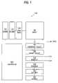
- FIG. 1is a system block diagram.
- FIG. 2is a schematic diagram.
- FIG. 3is a timing diagram.
- FIG. 4is a schematic diagram.
- FIG. 5is a schematic diagram.
- a monolithic integrated imaging circuit 100includes an array 102 of active pixel sensors and a controller 104 .
- the controller 104provides timing and control signals that facilitate reading out signals from the pixel sensors and that facilitate various other image processing functions.
- the dimensions of the array 102can vary depending on specific imaging requirements for a particular application. For example, array 102 might have dimensions such as 128 active pixel sensors by 128 active pixel sensors or more.
- channels 128can include one or more conductive paths that carry signals between circuit components.
- a read-out circuit 116is electrically coupled to the array 102 through a subgroup select module 108 and a group select module 106 .
- the read-out circuit 116can be a charge mode amplifier or other circuit responsive to a sensed charge.
- An active pixel sensor of array 102provides an output signal representative of a portion of an image, and the read-out circuit 116 receives the output signal.
- the subgroup select module 108 , group select module 106 and read-out circuit 108may include, for example, sample and hold circuitry, switching circuitry, and signal conditioning circuitry.
- the read-out circuitprovides an output signal in response to the signal received from an active pixel sensor of array 102 .
- the outputmay take the form, for example, of a differential signal on lines 124 and 126 , or a non-differential signal outputted to one or more lines.
- the imaging circuit 100also includes counter circuits 110 , 120 , decoder circuits 112 , 118 and other circuitry to support imaging circuit 100 operations.
- Such circuitrymay include for example, row select circuit module 114 , latches 122 and additional levels of select circuitry (not shown).
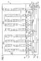
- the array 102includes subgroups 204 a , 204 b . . . 204 y of active pixel sensors 200 , that are organized into groups 202 a , 202 b . . . 202 g .
- Each group 202 a , 202 b . . . 202 gincludes one or more subgroups 204 a , 204 b . . . 204 y , for example, group 202 a includes subgroups 204 a , 204 b . . . 204 f .
- the subgroups 204 a , 204 b . . . 204 yare arranged as columns.
- each subgroup 204 a , 204 b . . . 204 ycan be arranged as rows or in other configurations.
- each subgroup 204 a , 204 b . . . 204 yincludes two output ports, each of which is electrically coupled by two output lines to an associated subgroup select circuit 206 a , 206 b . . . 206 y .
- each subgroup 204 a , 204 b . . . 204 ymay include only a single output port electrically coupled to an associated subgroup select circuit 206 a , 206 b . . . 206 y through one or more electrically conductive lines.
- the subgroup select circuits 206 a , 206 b . . . 206 yare represented as NMOS switches, however, the subgroup select circuits 206 a , 206 b . . . 206 y may include other circuitry such as, sample and hold circuitry, or other signal processing circuitry. Additionally, such circuits could be implemented using NMOS, PMOS or CMOS technologies.
- Each subgroup select circuit 206 a , 206 b . . . 206 yincludes output ports that are electrically coupled to a differential output bus 208 a , 208 b . . . 208 g .
- Each differential output bus 208 a , 208 b . . . 208 gmay include two or more conductive paths that electrically couple the output ports of all of the subgroup select circuits 206 a , 206 b . . . 206 y associated with a particular group 202 a , 202 b . . . 202 g to an input port of a respective group select circuit 210 a , 210 b . . . 210 g .
- the group select circuits 210 a , 210 b . . . 210 gcan be implemented using NMOS switches, although, other implementations may include PMOS or CMOS switches.
- Each group select circuit 210 a , 210 b . . . 210 gincludes output ports that can be electrically coupled to a common output bus 212 .
- This common output bus 212can be electrically coupled, for example, to input ports of a readout circuit 116 , such as a charge mode read-out amplifier or other signal processing circuit.
- the differential output buses 208 a , 208 b . . . 208 gare coupled to a set of clamping voltage switches 216 . These switches close when the respective differential output bus 208 a , 208 b . . . 208 g is electrically isolated from the read-out circuit 116 , to maintain the bus voltage at a predetermined clamp voltage value.
- the clamp voltagecan be, for example, the power supply voltage or a grounded connection. This can minimize signal distortion and undesirable leakage current in the system.
- the controller 104sends subgroup select signals C SS to the gate terminals of the subgroup select circuits 206 a , 206 b . . . 206 y to enable each subgroup select circuit 206 a , 206 b . . . 206 y to pass a signal from an active pixel sensor 200 of a respective subgroup 204 a , 204 b . . . 204 y to a respective differential bus 208 a , 208 b . . . 208 g .
- the controller 104also sends group select signals G SS to the gate terminals of the group select circuits 210 a , 210 b . . .
- each group select circuit 210 a , 210 b . . . 210 gto pass a signal from a respective subgroup select circuit 206 a , 206 b . . . 206 y to the common output bus 212 .
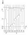
- FIG. 3is a control signal timing diagram 320 detailing the operation of readout circuit 116 .
- Group select signals G SS for each respective group select circuit 210 a , 210 b . . . 210 g and subgroup select signals C SS for each respective subgroup select circuit 206 a , 206 b . . . 206 yare shown as a function of time along a time axis 304 .
- the group select signals G SS and the subgroup select signals C SScan be, for example, voltage signals generated by the controller 104 or by another circuit or combination of circuits and power sources.
- the group select signals G SSare provided at gate terminals of each group select circuit 210 a , 210 b . . .
- each group select circuit 210 a , 210 b . . . 210 gto selectively enable each group select circuits 210 a , 210 b . . . 210 g to pass a signal between the respective drain and source terminals one at a time in a sequential manner.
- the subgroup select signals C SSare provided to gate terminals of each subgroup select circuit 206 a , 206 b . . . 206 y to selectively enable each subgroup select circuit 206 a , 206 b . . . 206 y to pass a signal between the respective drain and source terminals one at a time, in a sequential manner.
- a group select signal G SSis applied to the gate terminal of group select circuit 210 a establishing a conductive path between the drain and source terminals of group select circuit 210 a , thereby effectively “closing” the switch.
- a subgroup select signal C SSis applied to the gate terminals of subgroup select circuit 206 a establishing a conductive path between the drain and source terminals of the subgroup select circuit 206 a , thereby effectively “closing” the switch. Applying a subgroup select signal C SS to the gate terminals of subgroup select circuit 206 a thus enables the subgroup select circuit 206 a to pass a signal to the group select circuit 210 a .
- group select circuit 210 aapplies a group select signal G SS to the gate terminals of group select circuit 210 a enables the group select circuit 210 a to pass the signal to the common bus 212 .
- the readout circuit 116is isolated electrically from subgroup select circuits 206 b . . . 206 g that are associated with groups 202 b . . . 202 g.
- the charge mode read-out circuit 116can receive a signal from an active pixel sensor 200 in subgroup 204 a of group 202 a .
- the signalis passed from subgroup 204 a , to subgroup select circuit 206 a , to differential output bus 208 a , through group select circuit 210 a , to common differential output bus 212 , and then to readout circuit 116 .
- the group select signal G SS previously applied to group select circuit 210 ais maintained, but the subgroup select signal C SS previously applied to subgroup select circuit 206 a is changed to disable subgroup select circuit 206 a , effectively “opening” the switch. That has the effect of electrically isolating subgroup 204 a from the readout circuit 116 and electrically coupling subgroup 204 b to the readout circuit 116 .
- a subgroup select signal C SSis then applied to enable subgroup select circuit 206 b.
- a signal generated in a pixel of subgroup 204 bcan be passed from subgroup 204 b , to subgroup select circuit 206 b , to differential output bus 208 a , through group select circuit 210 a , to common differential output bus 212 , and to readout circuit 116 .
- the subgroup select signals C SSsequentially enable, one at a time, the subgroup select circuits 206 a , 206 b . . . 206 f that are coupled to the group select circuit 210 a .
- a group select signal G SSis applied at the gate terminals of group select circuit 210 a to maintain group select circuit 210 a in a conductive state.
- the group select signal G SS that was previously applied to group select circuit 210 ais removed and a new group select signal G SS is applied to group select circuit 210 b .
- the subgroup select signals C SSthen are sent, sequentially, to each subgroup select circuit 206 g , 206 h . . . 206 l coupled to group select circuit 210 b . While the group select circuit 210 b is in a conductive state, the readout circuit 116 is isolated electrically from the subgroup select circuits not associated with group 202 b.
- the read-out circuit 116continues in this manner to read-out signals sequentially from the subgroup select circuits 206 a , 206 b . . . 206 y until they all have been read and passed to readout circuit 116 .
- the particular order of pollingmay vary.
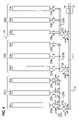
- FIG. 4illustrates how the techniques described herein can reduce parasitic capacitance present at the input terminals of an imager's readout circuit 116 .
- An array 102includes nine subgroups 204 a , 204 b . . . 204 i of active pixel sensors 200 .
- the subgroups 204 a , 204 b . . . 204 iare divided into three groups 202 a , 202 b , and 202 c .
- Each group 202 a , 202 b , and 202 cincludes three subgroups.
- group 202 aincludes subgroups 204 a , 204 b , and 204 c .
- Each subgroup 204 a , 204 b . . . 204 iincludes two output ports electrically coupled to a subgroup select circuit 206 a , 206 b . . . 206 i
- each subgroup select circuit 206 a , 206 b . . . 206 iincludes two output ports coupled electrically to a group select circuit 210 a , 210 b and 210 c associated with a particular group 202 a , 202 b , or 202 c .
- Each group select circuit 210 a , 210 b and 210 cincludes two output ports coupled electrically to a common differential output bus 212 which terminates at a readout circuit 116 .
- the readout circuit 116can amplify a signal it receives to facilitate further processing of the signal downstream of the readout circuit 116 .
- the readout circuit 116can require a considerable amount of power to accomplish these functions. The foregoing techniques can be used to help reduce the power requirements of the readout circuit 116 .
- Subgroup select circuits 206 a , 206 b . . . 206 i and group select circuits 210 a , 210 b , 210 chave associated values of parasitic capacitance values C par that are approximately the same for each circuit. Also, the approximate value of parasitic capacitance for a given switch does not change significantly whether the switch is in a conductive or a non-conductive state.
- the total parasitic capacitance that can be seen at the input terminals of the readout circuit 116is approximately equal to the sum of the parasitic capacitances of circuits 206 a , 206 b , 206 c , 210 a , 210 b , and 210 c , or six times C par . If group select circuits were not included in the implementation illustrated in FIG. 4 , the parasitic capacitance would be approximately equal to the sum of the parasitic capacitances of circuits 206 a , 206 . . .
- group select circuits 210 a , 210 b and 210 ccan provide a reduction in the parasitic capacitance from nine times C par to six times C par at the input terminals of the readout circuit 116 .
- a reduction of parasitic capacitancea corresponding reduction in capacitive current losses also can be realized. Accordingly, the power required by the readout circuit 116 can be reduced as well.
- the optimum number of group select circuits 210 a , 210 b , 210 c to minimize parasitic capacitance C parshould be approximately equal to the square root of the number of subgroup select circuits 206 a , 206 b . . . 206 i in the system. For example, if there are nine subgroup select circuits 206 a , 206 b . . . 206 i , then three group select circuits 210 a , 210 b and 210 c should be used. If additional levels of selection circuits are added downstream from the group select circuits 210 a , 210 b , 210 c , a similar design guideline may be applied.
- the number of selection circuits to be implemented for reducing parasitic capacitancecan be optimized. To do so, the number of selection circuits should be approximately equal to the square root of the number of selection circuits present in the layer immediately upstream from it.
- Some array designsinclude 100 subgroups, 280 subgroups, 480 subgroups or 900 subgroups. Each subgroup would have a corresponding subgroup select circuit. Based on the foregoing guideline for optimizing the number of group select circuits, the 100 subgroup select circuits would be coupled to approximately 10 group select circuits, the 280 subgroup select circuits would be coupled to approximately 17 group select circuits, the 480 subgroup select circuits would be coupled to approximately 22 group select circuits and the 900 subgroup select circuits would be coupled to approximately 30 group select circuits. In these examples, the ratio of subgroup select circuits to group select circuits ranges from approximately 10:1 to 40:1 and preferably from approximately 15:1 to 30:1.
- the techniquescan be applied to multiple levels of selection circuitry, implemented, for example, as a set of supergroup select circuits 500 a . . . 500 k .
- Each supergroup select circuit 500 a . . . 500 kis coupled to receive output signals from a set of group select circuits 210 a , 210 b . . . 210 y associated with a supergroup select circuit 500 a . . . 500 k .
- a supergroupcan be considered to be a group of groups.
- the controller 104can provide control signals at the gate terminals of each supergroup select circuit 500 a . . . 500 k to selectively enable each supergroup select circuits 500 a . . .
- Each supergroup select circuit 500 a . . . 500 kcan be implemented using a transistor switch with a respective gate terminal for receiving the control signal from the controller 104 .
- the control signalscan selectively enable each supergroup select circuit 500 a . . . 500 k in cooperation with the group select circuits 210 a , 210 b . . . 210 g and the subgroup select circuits 206 a , 206 b . . . 206 y to allow passage of signals from each subgroup select circuit 206 a , 206 b . . . 206 y to the readout circuit 116 , one at a time, sequentially, similarly as outlined in detail above.
Landscapes
- Engineering & Computer Science (AREA)
- Multimedia (AREA)
- Signal Processing (AREA)
- Transforming Light Signals Into Electric Signals (AREA)
Abstract
Description
Claims (23)
Priority Applications (2)
| Application Number | Priority Date | Filing Date | Title |
|---|---|---|---|
| US09/901,280US7088394B2 (en) | 2001-07-09 | 2001-07-09 | Charge mode active pixel sensor read-out circuit |
| US11/455,714US7649558B2 (en) | 2001-07-09 | 2006-06-20 | Charge mode active pixel sensor read-out circuit |
Applications Claiming Priority (1)
| Application Number | Priority Date | Filing Date | Title |
|---|---|---|---|
| US09/901,280US7088394B2 (en) | 2001-07-09 | 2001-07-09 | Charge mode active pixel sensor read-out circuit |
Related Child Applications (1)
| Application Number | Title | Priority Date | Filing Date |
|---|---|---|---|
| US11/455,714ContinuationUS7649558B2 (en) | 2001-07-09 | 2006-06-20 | Charge mode active pixel sensor read-out circuit |
Publications (2)
| Publication Number | Publication Date |
|---|---|
| US20030007083A1 US20030007083A1 (en) | 2003-01-09 |
| US7088394B2true US7088394B2 (en) | 2006-08-08 |
Family
ID=25413861
Family Applications (2)
| Application Number | Title | Priority Date | Filing Date |
|---|---|---|---|
| US09/901,280Expired - LifetimeUS7088394B2 (en) | 2001-07-09 | 2001-07-09 | Charge mode active pixel sensor read-out circuit |
| US11/455,714Expired - LifetimeUS7649558B2 (en) | 2001-07-09 | 2006-06-20 | Charge mode active pixel sensor read-out circuit |
Family Applications After (1)
| Application Number | Title | Priority Date | Filing Date |
|---|---|---|---|
| US11/455,714Expired - LifetimeUS7649558B2 (en) | 2001-07-09 | 2006-06-20 | Charge mode active pixel sensor read-out circuit |
Country Status (1)
| Country | Link |
|---|---|
| US (2) | US7088394B2 (en) |
Cited By (18)
| Publication number | Priority date | Publication date | Assignee | Title |
|---|---|---|---|---|
| US20060221414A1 (en)* | 2005-03-30 | 2006-10-05 | Denso Corporation | Image scanning device |
| US20090194672A1 (en)* | 2008-02-04 | 2009-08-06 | Tredwell Timothy J | Digital radiographic imaging apparatus |
| US20100149393A1 (en)* | 2008-05-22 | 2010-06-17 | Panavision Imaging, Llc | Increasing the resolution of color sub-pixel arrays |
| US20110205384A1 (en)* | 2010-02-24 | 2011-08-25 | Panavision Imaging, Llc | Variable active image area image sensor |
| US9023967B2 (en) | 2011-11-30 | 2015-05-05 | Chevron Phillips Chemical Company Lp | Long chain branched polymers and methods of making same |
| US9096699B2 (en) | 2011-12-02 | 2015-08-04 | Chevron Phillips Chemical Company Lp | Methods of preparing a catalyst |
| US9587048B2 (en) | 2015-04-29 | 2017-03-07 | Chevron Phillips Chemical Company Lp | Methods of preparing a catalyst |
| US9988468B2 (en) | 2016-09-30 | 2018-06-05 | Chevron Phillips Chemical Company Lp | Methods of preparing a catalyst |
| US10213766B2 (en) | 2015-09-18 | 2019-02-26 | Chevron Phillips Chemical Company Lp | Methods of preparing a catalyst |
| US10287369B2 (en) | 2017-04-24 | 2019-05-14 | Chevron Phillips Chemical Company Lp | Methods of preparing a catalyst |
| US10323109B2 (en) | 2017-11-17 | 2019-06-18 | Chevron Phillips Chemical Company Lp | Methods of preparing a catalyst utilizing hydrated reagents |
| US10513570B2 (en) | 2017-11-17 | 2019-12-24 | Chevron Phillips Chemical Company Lp | Methods of preparing a catalyst |
| US10543480B2 (en) | 2018-04-16 | 2020-01-28 | Chevron Phillips Chemical Company Lp | Methods of preparing a catalyst utilizing hydrated reagents |
| US10654953B2 (en) | 2016-12-29 | 2020-05-19 | Chevron Phillips Chemical Company Lp | Methods of preparing a catalyst |
| US10722874B2 (en) | 2018-04-16 | 2020-07-28 | Chevron Phillips Chemical Company Lp | Methods of preparing a catalyst utilizing hydrated reagents |
| US11266976B2 (en) | 2018-04-16 | 2022-03-08 | Chevron Phillips Chemical Company Lp | Methods of preparing a catalyst with low HRVOC emissions |
| US11267914B2 (en) | 2016-12-29 | 2022-03-08 | Chevron Phillips Chemical Company Lp | Methods of preparing a catalyst |
| US11472897B2 (en) | 2016-12-29 | 2022-10-18 | Chevron Phillips Chemical Company Lp | Methods of preparing a catalyst |
Families Citing this family (2)
| Publication number | Priority date | Publication date | Assignee | Title |
|---|---|---|---|---|
| US7700516B2 (en)* | 2007-09-26 | 2010-04-20 | Chevron Phillips Chemical Company Lp | Methods of preparing a polymerization catalyst |
| US8223236B2 (en)* | 2008-07-03 | 2012-07-17 | Sony Ericsson Mobile Communications Ab | Apparatus and method for image recording |
Citations (20)
| Publication number | Priority date | Publication date | Assignee | Title |
|---|---|---|---|---|
| US4551634A (en)* | 1982-03-31 | 1985-11-05 | Fujitsu Limited | Multiplexing input circuit |
| US4768098A (en)* | 1987-08-31 | 1988-08-30 | General Electric Company | CID imager with reduced crosstalk and method for operation thereof |
| US5134489A (en)* | 1990-12-28 | 1992-07-28 | David Sarnoff Research Center, Inc. | X-Y addressable solid state imager for low noise operation |
| US5148268A (en)* | 1991-04-26 | 1992-09-15 | Xerox Corporation | Multiplexing arrangement for controlling data produced by a color images sensor array |
| US5315102A (en)* | 1991-09-05 | 1994-05-24 | Fuji Xerox Co., Ltd. | Driving device and method for driving two-dimensional contact image sensor |
| US5471515A (en) | 1994-01-28 | 1995-11-28 | California Institute Of Technology | Active pixel sensor with intra-pixel charge transfer |
| US5550653A (en) | 1995-06-05 | 1996-08-27 | Xerox Corporation | Color sensor array and system for scanning simple color documents |
| US5631704A (en) | 1994-10-14 | 1997-05-20 | Lucent Technologies, Inc. | Active pixel sensor and imaging system having differential mode |
| US5715204A (en)* | 1994-05-03 | 1998-02-03 | Sgs-Thomson Microelectronics, S.R.L. | Sense amplifier with hysteresis |
| US5739562A (en) | 1995-08-01 | 1998-04-14 | Lucent Technologies Inc. | Combined photogate and photodiode active pixel image sensor |
| US5789736A (en)* | 1993-09-16 | 1998-08-04 | Nec Corporation | Signal readout circuit having a two-dimensional focal plane cell array capable of reading out signals with improved resolution |
| US5841126A (en) | 1994-01-28 | 1998-11-24 | California Institute Of Technology | CMOS active pixel sensor type imaging system on a chip |
| US5854656A (en) | 1995-11-15 | 1998-12-29 | Logitech, Inc. | Non-uniform clocking system for area imaging device |
| US5949483A (en)* | 1994-01-28 | 1999-09-07 | California Institute Of Technology | Active pixel sensor array with multiresolution readout |
| US6252217B1 (en)* | 1997-12-18 | 2001-06-26 | Simage Oy | Device for imaging radiation |
| US6320618B1 (en)* | 1996-08-30 | 2001-11-20 | Honda Giken Kogyo Kabushiki Kaisha | Semiconductor image sensor with a plurality of different resolution areas |
| US6366320B1 (en)* | 1997-12-08 | 2002-04-02 | Intel Corporation | High speed readout architecture for analog storage arrays |
| US20020179820A1 (en)* | 2000-11-27 | 2002-12-05 | Moshe Stark | Noise floor reduction in image sensors |
| US6512546B1 (en)* | 1998-07-17 | 2003-01-28 | Analog Devices, Inc. | Image sensor using multiple array readout lines |
| US6535576B2 (en)* | 2000-12-29 | 2003-03-18 | Ge Medical Systems Global Technology Company, Llc | Enhanced digital detector and system and method incorporating same |
Family Cites Families (2)
| Publication number | Priority date | Publication date | Assignee | Title |
|---|---|---|---|---|
| JPH0822002B2 (en)* | 1990-03-27 | 1996-03-04 | 富士ゼロックス株式会社 | Image sensor and driving method thereof |
| GB2289983B (en)* | 1994-06-01 | 1996-10-16 | Simage Oy | Imaging devices,systems and methods |
- 2001
- 2001-07-09USUS09/901,280patent/US7088394B2/ennot_activeExpired - Lifetime
- 2006
- 2006-06-20USUS11/455,714patent/US7649558B2/ennot_activeExpired - Lifetime
Patent Citations (20)
| Publication number | Priority date | Publication date | Assignee | Title |
|---|---|---|---|---|
| US4551634A (en)* | 1982-03-31 | 1985-11-05 | Fujitsu Limited | Multiplexing input circuit |
| US4768098A (en)* | 1987-08-31 | 1988-08-30 | General Electric Company | CID imager with reduced crosstalk and method for operation thereof |
| US5134489A (en)* | 1990-12-28 | 1992-07-28 | David Sarnoff Research Center, Inc. | X-Y addressable solid state imager for low noise operation |
| US5148268A (en)* | 1991-04-26 | 1992-09-15 | Xerox Corporation | Multiplexing arrangement for controlling data produced by a color images sensor array |
| US5315102A (en)* | 1991-09-05 | 1994-05-24 | Fuji Xerox Co., Ltd. | Driving device and method for driving two-dimensional contact image sensor |
| US5789736A (en)* | 1993-09-16 | 1998-08-04 | Nec Corporation | Signal readout circuit having a two-dimensional focal plane cell array capable of reading out signals with improved resolution |
| US5471515A (en) | 1994-01-28 | 1995-11-28 | California Institute Of Technology | Active pixel sensor with intra-pixel charge transfer |
| US5841126A (en) | 1994-01-28 | 1998-11-24 | California Institute Of Technology | CMOS active pixel sensor type imaging system on a chip |
| US5949483A (en)* | 1994-01-28 | 1999-09-07 | California Institute Of Technology | Active pixel sensor array with multiresolution readout |
| US5715204A (en)* | 1994-05-03 | 1998-02-03 | Sgs-Thomson Microelectronics, S.R.L. | Sense amplifier with hysteresis |
| US5631704A (en) | 1994-10-14 | 1997-05-20 | Lucent Technologies, Inc. | Active pixel sensor and imaging system having differential mode |
| US5550653A (en) | 1995-06-05 | 1996-08-27 | Xerox Corporation | Color sensor array and system for scanning simple color documents |
| US5739562A (en) | 1995-08-01 | 1998-04-14 | Lucent Technologies Inc. | Combined photogate and photodiode active pixel image sensor |
| US5854656A (en) | 1995-11-15 | 1998-12-29 | Logitech, Inc. | Non-uniform clocking system for area imaging device |
| US6320618B1 (en)* | 1996-08-30 | 2001-11-20 | Honda Giken Kogyo Kabushiki Kaisha | Semiconductor image sensor with a plurality of different resolution areas |
| US6366320B1 (en)* | 1997-12-08 | 2002-04-02 | Intel Corporation | High speed readout architecture for analog storage arrays |
| US6252217B1 (en)* | 1997-12-18 | 2001-06-26 | Simage Oy | Device for imaging radiation |
| US6512546B1 (en)* | 1998-07-17 | 2003-01-28 | Analog Devices, Inc. | Image sensor using multiple array readout lines |
| US20020179820A1 (en)* | 2000-11-27 | 2002-12-05 | Moshe Stark | Noise floor reduction in image sensors |
| US6535576B2 (en)* | 2000-12-29 | 2003-03-18 | Ge Medical Systems Global Technology Company, Llc | Enhanced digital detector and system and method incorporating same |
Non-Patent Citations (2)
| Title |
|---|
| Mendis et al., "CMOS Active Pixel Image Sensor," IEEE Transactions on Electron Devices, vol. 41, No. 3, Mar. 1994, pp. 452-453. |
| Mendis et al., "Progress in CMOS Active Pixel Image Sensors," Proceedings of the SPIE vol. 2172, Charge-Coupled Devices and Solid State Optical Sensors IV (1994). |
Cited By (43)
| Publication number | Priority date | Publication date | Assignee | Title |
|---|---|---|---|---|
| US20060221414A1 (en)* | 2005-03-30 | 2006-10-05 | Denso Corporation | Image scanning device |
| US7643076B2 (en)* | 2005-03-30 | 2010-01-05 | Denso Corporation | Image scanning device having multiple CMOS element in matrix form |
| US20090194672A1 (en)* | 2008-02-04 | 2009-08-06 | Tredwell Timothy J | Digital radiographic imaging apparatus |
| US7619197B2 (en)* | 2008-02-04 | 2009-11-17 | Carestream Health, Inc. | Digital radiographic imaging apparatus |
| US20100149393A1 (en)* | 2008-05-22 | 2010-06-17 | Panavision Imaging, Llc | Increasing the resolution of color sub-pixel arrays |
| US20110205384A1 (en)* | 2010-02-24 | 2011-08-25 | Panavision Imaging, Llc | Variable active image area image sensor |
| WO2011106568A1 (en)* | 2010-02-24 | 2011-09-01 | Panavision Imaging, Llc | Variable active image area image sensor |
| US9879101B2 (en) | 2011-11-30 | 2018-01-30 | Chevron Phillips Chemical Company, Lp | Long chain branched polymers and methods of making same |
| US9598513B2 (en) | 2011-11-30 | 2017-03-21 | Chevron Phillips Chemical Company Lp | Long chain branched polymers and methods of making same |
| US9023967B2 (en) | 2011-11-30 | 2015-05-05 | Chevron Phillips Chemical Company Lp | Long chain branched polymers and methods of making same |
| US10323108B2 (en) | 2011-11-30 | 2019-06-18 | Chevron Phillips Chemical Company Lp | Long chain branched polymers and methods of making same |
| US9096699B2 (en) | 2011-12-02 | 2015-08-04 | Chevron Phillips Chemical Company Lp | Methods of preparing a catalyst |
| US9587048B2 (en) | 2015-04-29 | 2017-03-07 | Chevron Phillips Chemical Company Lp | Methods of preparing a catalyst |
| US9796798B2 (en) | 2015-04-29 | 2017-10-24 | Chevron Phillips Chemical Company, Lp | Methods of preparing a catalyst |
| US10213766B2 (en) | 2015-09-18 | 2019-02-26 | Chevron Phillips Chemical Company Lp | Methods of preparing a catalyst |
| US11801490B2 (en) | 2015-09-18 | 2023-10-31 | Chevron Phillips Chemical Company Lp | Methods of preparing a catalyst |
| US9988468B2 (en) | 2016-09-30 | 2018-06-05 | Chevron Phillips Chemical Company Lp | Methods of preparing a catalyst |
| US10654953B2 (en) | 2016-12-29 | 2020-05-19 | Chevron Phillips Chemical Company Lp | Methods of preparing a catalyst |
| US11267914B2 (en) | 2016-12-29 | 2022-03-08 | Chevron Phillips Chemical Company Lp | Methods of preparing a catalyst |
| US11976142B2 (en) | 2016-12-29 | 2024-05-07 | Chevron Phillips Chemical Company Lp | Methods of preparing a catalyst |
| US11697697B2 (en) | 2016-12-29 | 2023-07-11 | Chevron Phillips Chemical Company Lp | Methods of preparing a catalyst |
| US11472897B2 (en) | 2016-12-29 | 2022-10-18 | Chevron Phillips Chemical Company Lp | Methods of preparing a catalyst |
| US10287369B2 (en) | 2017-04-24 | 2019-05-14 | Chevron Phillips Chemical Company Lp | Methods of preparing a catalyst |
| US11542348B2 (en) | 2017-11-17 | 2023-01-03 | Chevron Phillips Chemical Company Lp | Methods of preparing a catalyst |
| US10858460B2 (en) | 2017-11-17 | 2020-12-08 | Chevron Phillips Chemical Company Lp | Methods of preparing a catalyst utilizing hydrated reagents |
| US10323109B2 (en) | 2017-11-17 | 2019-06-18 | Chevron Phillips Chemical Company Lp | Methods of preparing a catalyst utilizing hydrated reagents |
| US10988557B2 (en) | 2017-11-17 | 2021-04-27 | Chevron Phillips Chemical Company Lp | Methods of preparing a catalyst utilizing hydrated reagents |
| US10513570B2 (en) | 2017-11-17 | 2019-12-24 | Chevron Phillips Chemical Company Lp | Methods of preparing a catalyst |
| US11384179B2 (en) | 2017-11-17 | 2022-07-12 | Chevron Phillips Chemical Company Lp | Methods of preparing a catalyst |
| US11117122B2 (en) | 2018-04-16 | 2021-09-14 | Chevron Phillips Chemical Company Lp | Methods of preparing a catalyst utilizing hydrated reagents |
| US11110443B2 (en) | 2018-04-16 | 2021-09-07 | Chevron Phillips Chemical Company Lp | Methods of preparing a catalyst utilizing hydrated reagents |
| US11358131B2 (en) | 2018-04-16 | 2022-06-14 | Chevron Phillips Chemical Company Lp | Methods of preparing a catalyst utilizing hydrated reagents |
| US11358132B2 (en) | 2018-04-16 | 2022-06-14 | Chevron Phillips Chemical Company Lp | Methods of preparing a catalyst utilizing hydrated reagents |
| US10894250B2 (en) | 2018-04-16 | 2021-01-19 | Chevron Phillips Chemical Company Lp | Methods of preparing a catalyst utilizing hydrated reagents |
| US11383222B2 (en) | 2018-04-16 | 2022-07-12 | Chevron Phillips Chemical Company Lp | Methods of preparing a catalyst with low HRVOC emissions |
| US10821428B2 (en) | 2018-04-16 | 2020-11-03 | Chevron Phillips Chemical Company Lp | Methods of preparing a catalyst utilizing hydrated reagents |
| US11266976B2 (en) | 2018-04-16 | 2022-03-08 | Chevron Phillips Chemical Company Lp | Methods of preparing a catalyst with low HRVOC emissions |
| US11583841B2 (en) | 2018-04-16 | 2023-02-21 | Chevron Phillips Chemical Company Lp | Methods of preparing a catalyst utilizing hydrated reagents |
| US11583840B2 (en) | 2018-04-16 | 2023-02-21 | Chevron Phillips Chemical Company Lp | Methods of preparing a catalyst utilizing hydrated reagents |
| US10722874B2 (en) | 2018-04-16 | 2020-07-28 | Chevron Phillips Chemical Company Lp | Methods of preparing a catalyst utilizing hydrated reagents |
| US10894249B2 (en) | 2018-04-16 | 2021-01-19 | Chevron Phillips Chemical Company Lp | Methods of preparing a catalyst utilizing hydrated reagents |
| US10543480B2 (en) | 2018-04-16 | 2020-01-28 | Chevron Phillips Chemical Company Lp | Methods of preparing a catalyst utilizing hydrated reagents |
| US12005425B2 (en) | 2018-04-16 | 2024-06-11 | Chevron Phillips Chemical Company Lp | Methods of preparing a catalyst with low HRVOC emissions |
Also Published As
| Publication number | Publication date |
|---|---|
| US20060278812A1 (en) | 2006-12-14 |
| US20030007083A1 (en) | 2003-01-09 |
| US7649558B2 (en) | 2010-01-19 |
Similar Documents
| Publication | Publication Date | Title |
|---|---|---|
| US7649558B2 (en) | Charge mode active pixel sensor read-out circuit | |
| USRE34908E (en) | 3-transistor source follower-per-detector unit cell for 2-dimensional focal plane arrays | |
| US7525587B2 (en) | Image sensors with pixel reset | |
| US5382977A (en) | Electronically scanned buffered direct injection circuit for staring IR focal plane array | |
| US7068319B2 (en) | CMOS image sensor with a low-power architecture | |
| US8947277B2 (en) | Multi-channel sample-and-hold circuit and analog-to-digital converter using the same | |
| US8582008B2 (en) | Fast-settling line driver design for high resolution video IR and visible images | |
| EP0585115B1 (en) | Analog multiplexer with standby mode | |
| US11606524B2 (en) | CTIA CMOS image sensor pixel with zero-biased multiplexer | |
| US8102451B2 (en) | VLN biasing scheme to achieve low vertical shading for high-speed and large-format CMOS image sensors with top/bottom readout scheme | |
| GB2387985A (en) | Multiplexing circuit for imaging device | |
| US20050237406A1 (en) | CMOS image sensor for processing analog signal at high speed | |
| US6747700B1 (en) | Solid state image pickup apparatus having a plurality of split buses | |
| US6693270B2 (en) | Current mode analog signal multiplexing bus and a method thereof | |
| JP2000228100A (en) | Readout device with array configuration | |
| US20080061830A1 (en) | Method, apparatus, and system providing power supply independent imager output driver having a constant slew rate | |
| EP0865684B1 (en) | Charge measurement circuit | |
| EP1139563B1 (en) | Analog fifo memory | |
| TWI882263B (en) | Digital-to-analog signal converter and image sensor including the same | |
| US11431931B2 (en) | CTIA pixel with shared reset network | |
| US20020185602A1 (en) | Method of multiplexing column amplifiers in a resistive bolometer array | |
| US6563103B1 (en) | Image sensor and method of operating an image sensor | |
| EP0951142A2 (en) | Cmos imager column buffer gain compensation circuit | |
| KR20230071040A (en) | Digital-to-analog converter and image sensor including the same | |
| HU207189B (en) | Switching arrangement for wide-band signals |
Legal Events
| Date | Code | Title | Description |
|---|---|---|---|
| AS | Assignment | Owner name:PHOTOBIT CORPORATION, CALIFORNIA Free format text:ASSIGNMENT OF ASSIGNORS INTEREST;ASSIGNORS:ROSSI, GIUSEPPE;BARNA, SANDOR L.;REEL/FRAME:011986/0701 Effective date:20010706 | |
| AS | Assignment | Owner name:MICRON TECHNOLOGY, INC., IDAHO Free format text:ASSIGNMENT OF ASSIGNORS INTEREST;ASSIGNOR:PHOTOBIT CORPORATION;REEL/FRAME:014007/0590 Effective date:20011121 Owner name:MICRON TECHNOLOGY, INC., IDAHO Free format text:ASSIGNMENT OF ASSIGNORS INTEREST;ASSIGNOR:PHOTOBIT CORPORATION;REEL/FRAME:012745/0385 Effective date:20011121 | |
| STCF | Information on status: patent grant | Free format text:PATENTED CASE | |
| FEPP | Fee payment procedure | Free format text:PAYOR NUMBER ASSIGNED (ORIGINAL EVENT CODE: ASPN); ENTITY STATUS OF PATENT OWNER: LARGE ENTITY | |
| AS | Assignment | Owner name:APTINA IMAGING CORPORATION, CAYMAN ISLANDS Free format text:ASSIGNMENT OF ASSIGNORS INTEREST;ASSIGNOR:MICRON TECHNOLOGY, INC.;REEL/FRAME:022694/0690 Effective date:20080926 | |
| AS | Assignment | Owner name:APTINA IMAGING CORPORATION, CAYMAN ISLANDS Free format text:ASSIGNMENT OF ASSIGNORS INTEREST;ASSIGNOR:MICRON TECHNOLOGY, INC.;REEL/FRAME:023245/0186 Effective date:20080926 Owner name:APTINA IMAGING CORPORATION,CAYMAN ISLANDS Free format text:ASSIGNMENT OF ASSIGNORS INTEREST;ASSIGNOR:MICRON TECHNOLOGY, INC.;REEL/FRAME:023245/0186 Effective date:20080926 | |
| FPAY | Fee payment | Year of fee payment:4 | |
| FPAY | Fee payment | Year of fee payment:8 | |
| MAFP | Maintenance fee payment | Free format text:PAYMENT OF MAINTENANCE FEE, 12TH YEAR, LARGE ENTITY (ORIGINAL EVENT CODE: M1553) Year of fee payment:12 |