US7087538B2 - Method to fill the gap between coupled wafers - Google Patents
Method to fill the gap between coupled wafersDownload PDFInfo
- Publication number
- US7087538B2 US7087538B2US10/919,550US91955004AUS7087538B2US 7087538 B2US7087538 B2US 7087538B2US 91955004 AUS91955004 AUS 91955004AUS 7087538 B2US7087538 B2US 7087538B2
- Authority
- US
- United States
- Prior art keywords
- wafer
- gap
- hole
- coupled
- pair
- Prior art date
- Legal status (The legal status is an assumption and is not a legal conclusion. Google has not performed a legal analysis and makes no representation as to the accuracy of the status listed.)
- Expired - Lifetime
Links
Images


Classifications
- H—ELECTRICITY
- H01—ELECTRIC ELEMENTS
- H01L—SEMICONDUCTOR DEVICES NOT COVERED BY CLASS H10
- H01L23/00—Details of semiconductor or other solid state devices
- H01L23/562—Protection against mechanical damage
- H—ELECTRICITY
- H01—ELECTRIC ELEMENTS
- H01L—SEMICONDUCTOR DEVICES NOT COVERED BY CLASS H10
- H01L25/00—Assemblies consisting of a plurality of semiconductor or other solid state devices
- H01L25/50—Multistep manufacturing processes of assemblies consisting of devices, the devices being individual devices of subclass H10D or integrated devices of class H10
- H—ELECTRICITY
- H01—ELECTRIC ELEMENTS
- H01L—SEMICONDUCTOR DEVICES NOT COVERED BY CLASS H10
- H01L21/00—Processes or apparatus adapted for the manufacture or treatment of semiconductor or solid state devices or of parts thereof
- H01L21/02—Manufacture or treatment of semiconductor devices or of parts thereof
- H01L21/04—Manufacture or treatment of semiconductor devices or of parts thereof the devices having potential barriers, e.g. a PN junction, depletion layer or carrier concentration layer
- H01L21/50—Assembly of semiconductor devices using processes or apparatus not provided for in a single one of the groups H01L21/18 - H01L21/326 or H10D48/04 - H10D48/07 e.g. sealing of a cap to a base of a container
- H01L21/56—Encapsulations, e.g. encapsulation layers, coatings
- H01L21/563—Encapsulation of active face of flip-chip device, e.g. underfilling or underencapsulation of flip-chip, encapsulation preform on chip or mounting substrate
- H—ELECTRICITY
- H01—ELECTRIC ELEMENTS
- H01L—SEMICONDUCTOR DEVICES NOT COVERED BY CLASS H10
- H01L2224/00—Indexing scheme for arrangements for connecting or disconnecting semiconductor or solid-state bodies and methods related thereto as covered by H01L24/00
- H01L2224/01—Means for bonding being attached to, or being formed on, the surface to be connected, e.g. chip-to-package, die-attach, "first-level" interconnects; Manufacturing methods related thereto
- H01L2224/02—Bonding areas; Manufacturing methods related thereto
- H01L2224/04—Structure, shape, material or disposition of the bonding areas prior to the connecting process
- H01L2224/05—Structure, shape, material or disposition of the bonding areas prior to the connecting process of an individual bonding area
- H01L2224/0554—External layer
- H01L2224/05573—Single external layer
- H—ELECTRICITY
- H01—ELECTRIC ELEMENTS
- H01L—SEMICONDUCTOR DEVICES NOT COVERED BY CLASS H10
- H01L2224/00—Indexing scheme for arrangements for connecting or disconnecting semiconductor or solid-state bodies and methods related thereto as covered by H01L24/00
- H01L2224/01—Means for bonding being attached to, or being formed on, the surface to be connected, e.g. chip-to-package, die-attach, "first-level" interconnects; Manufacturing methods related thereto
- H01L2224/02—Bonding areas; Manufacturing methods related thereto
- H01L2224/04—Structure, shape, material or disposition of the bonding areas prior to the connecting process
- H01L2224/05—Structure, shape, material or disposition of the bonding areas prior to the connecting process of an individual bonding area
- H01L2224/0554—External layer
- H01L2224/05599—Material
- H01L2224/056—Material with a principal constituent of the material being a metal or a metalloid, e.g. boron [B], silicon [Si], germanium [Ge], arsenic [As], antimony [Sb], tellurium [Te] and polonium [Po], and alloys thereof
- H01L2224/05638—Material with a principal constituent of the material being a metal or a metalloid, e.g. boron [B], silicon [Si], germanium [Ge], arsenic [As], antimony [Sb], tellurium [Te] and polonium [Po], and alloys thereof the principal constituent melting at a temperature of greater than or equal to 950°C and less than 1550°C
- H01L2224/05647—Copper [Cu] as principal constituent
- H—ELECTRICITY
- H01—ELECTRIC ELEMENTS
- H01L—SEMICONDUCTOR DEVICES NOT COVERED BY CLASS H10
- H01L2224/00—Indexing scheme for arrangements for connecting or disconnecting semiconductor or solid-state bodies and methods related thereto as covered by H01L24/00
- H01L2224/01—Means for bonding being attached to, or being formed on, the surface to be connected, e.g. chip-to-package, die-attach, "first-level" interconnects; Manufacturing methods related thereto
- H01L2224/10—Bump connectors; Manufacturing methods related thereto
- H01L2224/12—Structure, shape, material or disposition of the bump connectors prior to the connecting process
- H01L2224/13—Structure, shape, material or disposition of the bump connectors prior to the connecting process of an individual bump connector
- H01L2224/13001—Core members of the bump connector
- H01L2224/1302—Disposition
- H01L2224/13025—Disposition the bump connector being disposed on a via connection of the semiconductor or solid-state body
- H—ELECTRICITY
- H01—ELECTRIC ELEMENTS
- H01L—SEMICONDUCTOR DEVICES NOT COVERED BY CLASS H10
- H01L2224/00—Indexing scheme for arrangements for connecting or disconnecting semiconductor or solid-state bodies and methods related thereto as covered by H01L24/00
- H01L2224/01—Means for bonding being attached to, or being formed on, the surface to be connected, e.g. chip-to-package, die-attach, "first-level" interconnects; Manufacturing methods related thereto
- H01L2224/10—Bump connectors; Manufacturing methods related thereto
- H01L2224/12—Structure, shape, material or disposition of the bump connectors prior to the connecting process
- H01L2224/13—Structure, shape, material or disposition of the bump connectors prior to the connecting process of an individual bump connector
- H01L2224/13001—Core members of the bump connector
- H01L2224/13099—Material
- H01L2224/131—Material with a principal constituent of the material being a metal or a metalloid, e.g. boron [B], silicon [Si], germanium [Ge], arsenic [As], antimony [Sb], tellurium [Te] and polonium [Po], and alloys thereof
- H01L2224/13138—Material with a principal constituent of the material being a metal or a metalloid, e.g. boron [B], silicon [Si], germanium [Ge], arsenic [As], antimony [Sb], tellurium [Te] and polonium [Po], and alloys thereof the principal constituent melting at a temperature of greater than or equal to 950°C and less than 1550°C
- H01L2224/13147—Copper [Cu] as principal constituent
- H—ELECTRICITY
- H01—ELECTRIC ELEMENTS
- H01L—SEMICONDUCTOR DEVICES NOT COVERED BY CLASS H10
- H01L2224/00—Indexing scheme for arrangements for connecting or disconnecting semiconductor or solid-state bodies and methods related thereto as covered by H01L24/00
- H01L2224/80—Methods for connecting semiconductor or other solid state bodies using means for bonding being attached to, or being formed on, the surface to be connected
- H01L2224/83—Methods for connecting semiconductor or other solid state bodies using means for bonding being attached to, or being formed on, the surface to be connected using a layer connector
- H01L2224/831—Methods for connecting semiconductor or other solid state bodies using means for bonding being attached to, or being formed on, the surface to be connected using a layer connector the layer connector being supplied to the parts to be connected in the bonding apparatus
- H01L2224/83102—Methods for connecting semiconductor or other solid state bodies using means for bonding being attached to, or being formed on, the surface to be connected using a layer connector the layer connector being supplied to the parts to be connected in the bonding apparatus using surface energy, e.g. capillary forces
- H—ELECTRICITY
- H01—ELECTRIC ELEMENTS
- H01L—SEMICONDUCTOR DEVICES NOT COVERED BY CLASS H10
- H01L2224/00—Indexing scheme for arrangements for connecting or disconnecting semiconductor or solid-state bodies and methods related thereto as covered by H01L24/00
- H01L2224/91—Methods for connecting semiconductor or solid state bodies including different methods provided for in two or more of groups H01L2224/80 - H01L2224/90
- H01L2224/92—Specific sequence of method steps
- H01L2224/921—Connecting a surface with connectors of different types
- H01L2224/9212—Sequential connecting processes
- H01L2224/92122—Sequential connecting processes the first connecting process involving a bump connector
- H01L2224/92125—Sequential connecting processes the first connecting process involving a bump connector the second connecting process involving a layer connector
- H—ELECTRICITY
- H01—ELECTRIC ELEMENTS
- H01L—SEMICONDUCTOR DEVICES NOT COVERED BY CLASS H10
- H01L25/00—Assemblies consisting of a plurality of semiconductor or other solid state devices
- H01L25/03—Assemblies consisting of a plurality of semiconductor or other solid state devices all the devices being of a type provided for in a single subclass of subclasses H10B, H10D, H10F, H10H, H10K or H10N, e.g. assemblies of rectifier diodes
- H01L25/04—Assemblies consisting of a plurality of semiconductor or other solid state devices all the devices being of a type provided for in a single subclass of subclasses H10B, H10D, H10F, H10H, H10K or H10N, e.g. assemblies of rectifier diodes the devices not having separate containers
- H01L25/065—Assemblies consisting of a plurality of semiconductor or other solid state devices all the devices being of a type provided for in a single subclass of subclasses H10B, H10D, H10F, H10H, H10K or H10N, e.g. assemblies of rectifier diodes the devices not having separate containers the devices being of a type provided for in group H10D89/00
- H01L25/0657—Stacked arrangements of devices
- H—ELECTRICITY
- H01—ELECTRIC ELEMENTS
- H01L—SEMICONDUCTOR DEVICES NOT COVERED BY CLASS H10
- H01L2924/00—Indexing scheme for arrangements or methods for connecting or disconnecting semiconductor or solid-state bodies as covered by H01L24/00
- H01L2924/0001—Technical content checked by a classifier
- H01L2924/00014—Technical content checked by a classifier the subject-matter covered by the group, the symbol of which is combined with the symbol of this group, being disclosed without further technical details
- Y—GENERAL TAGGING OF NEW TECHNOLOGICAL DEVELOPMENTS; GENERAL TAGGING OF CROSS-SECTIONAL TECHNOLOGIES SPANNING OVER SEVERAL SECTIONS OF THE IPC; TECHNICAL SUBJECTS COVERED BY FORMER USPC CROSS-REFERENCE ART COLLECTIONS [XRACs] AND DIGESTS
- Y10—TECHNICAL SUBJECTS COVERED BY FORMER USPC
- Y10S—TECHNICAL SUBJECTS COVERED BY FORMER USPC CROSS-REFERENCE ART COLLECTIONS [XRACs] AND DIGESTS
- Y10S438/00—Semiconductor device manufacturing: process
- Y10S438/906—Cleaning of wafer as interim step
Definitions
- the present inventionrelates to the field of three dimensional integrated circuits and more specifically, to a method for forming a coupled wafer pair that prevents edge chipping.
- Stacking of the dice of a multi-processor microelectronic deviceis one way to improve the packaging density of a microelectronic device.
- Stacked microelectronic devicesare typically formed by electrically connecting two or more wafers through interconnect layers, and then dicing the stacked wafers into individual stacked devices.
- FIGS. 1A–1Dillustrate one method for forming a coupled wafer pair.
- a first wafer 101 and a second wafer 102are provided.
- these wafersare silicon polycrystalline wafers which have a plurality of die that are connected together.
- each dieis an integrated circuit.
- an interconnect layer 103is formed on the first wafer 101 and on the second wafer 102 .
- the interconnect layer 103is typically copper that is formed above a barrier material such as tantalum and a dielectric layer such as silicon dioxide or carbon dioxide.
- a barrier materialsuch as tantalum
- a dielectric layersuch as silicon dioxide or carbon dioxide.
- the first wafer 101 and its associated interconnect layer 103is flipped around and positioned over the second wafer 102 and its interconnect layer 103 .
- a coupled wafer pair 100is formed by aligning the interconnect layers 103 of the first wafer 101 and the second wafer 102 and bringing the first wafer 101 and the second wafer 102 together.
- a thermo-compression processis used to couple the first wafer 101 with the second wafer 102 .
- thinning 107 of one of the stacked wafersis performed by use of one or more mechanical and/or chemical processes such as a polishing process for example. These processes may cause mechanical stresses in unsupported portions of the wafer being thinned. As shown in an outer gap 106 , an area formed by the product of a depth 105 and a height 104 is unsupported by the interconnect layer 103 . Furthermore, a center gap 108 between individual members of the interconnect layer 103 may also be unsupported.
- FIGS. 1A–1Dillustrates a conventional method of forming a coupled wafer pair.
- FIGS. 2A–2Billustrates a method for applying a material on top of a first wafer of a coupled wafer pair in accordance with an embodiment of the present invention.
- FIGS. 3A–3Billustrates a method for applying a material directly in a gap between a coupled wafer pair in accordance with an embodiment of the present invention.
- FIGS. 4A–4Billustrates a method for applying a material through a hole in a first wafer of a coupled wafer pair in accordance with an embodiment of the present invention.
- FIGS. 5A–5Billustrates a method for applying a material through a hole in a first wafer of a coupled wafer pair and spinning the coupled wafer pair in accordance with an embodiment of the present invention.
- FIG. 6illustrates a process flow for creating a pressure differential to assist a material in filling a gap between a coupled wafer pair having at least one hole.
- FIGS. 7A–7Billustrates a method for applying a material directly in a gap between a coupled wafer pair and applying a vacuum through a hole in a first wafer of the coupled wafer pair in accordance with an embodiment of the present invention.
- FIGS. 8A–8Billustrates a method for applying a material through a hole in a first wafer of a coupled wafer pair, spinning the coupled wafer pair, and applying a vacuum directly in a gap between the coupled wafer pair in accordance with an embodiment of the present invention.
- FIGS. 9A–9Billustrates a method for applying a material and a positive pressure through a hole in a first wafer of a coupled wafer pair, spinning the coupled wafer pair, and applying a vacuum directly in a gap between the coupled wafer pair in accordance with an embodiment of the present invention.
- FIG. 10illustrates a top view of a coupled wafer pair having a plurality of dice and a gap fill in accordance with an embodiment of the present invention.
- FIG. 11illustrates a die that is cut from a coupled wafer pair having a gap fill in accordance with an embodiment of the present invention.
- Embodiments of the present inventionare three dimensional integrated circuit devices having a gap fill and their methods of formation.
- numerous specific detailshave been set forth in order to provide a thorough understanding of the present invention.
- well-known semiconductor fabrication processes and techniqueshave not been set forth in particular detail in order to avoid unnecessarily obscuring the present invention.
- Embodiments of the present inventionare a method for applying a material on a coupled wafer pair in order to fill a gap between wafers of the coupled wafer pair.
- Embodiments of the inventioninclude applying a material through a hole within one of the wafers of the coupled wafer pair and creating a pressure differential to help the material flow between the coupled wafers.
- Embodiments of the inventioninclude spinning a coupled wafer pair, applying a material on the top of or directly in a gap between the coupled wafer pair, and using a vacuum to create a pressure differential between the coupled wafers.
- the advantages of the present inventioninclude protecting gaps between a coupled wafer pair from chipping, cracking, corroding, or other damage which may result in the wafer and/or individual stacked devices being unusable.
- FIGS. 2A–2BAn example of a method for applying a material on top of a first wafer 201 of a coupled wafer pair 200 in accordance with an embodiment of the present invention is illustrated in FIGS. 2A–2B .
- the coupled wafer pairis formed similarly as described with reference to FIGS. 1A–1D .
- the coupled wafer pair 200is placed over a chuck 210 having a plurality of vacuum ports 211 .
- the vacuum ports 211generate a vacuum to secure the coupled wafer pair 200 to the chuck 210 .
- the chuck 210 and the coupled wafer pair 200are spun around at a first spin speed.
- the first spin speedis approximately 500–3,000 rotations per minute.
- the first spin speedis performed at a rate of at least 1000 rpm for approximately 20 seconds if the first wafer 201 and a second wafer 202 are 300 mm in diameter.
- an applicator 209applies a material 208 on top of the coupled wafer 200 .
- the material 208is applied at the center over the top of the wafer 201 .
- the material 208is applied anywhere on top of the wafer 201 .
- the applicator 209is a syringe.
- the applicator 209is a dispenser nozzle.
- an applicator 219instead of the applicator 209 , applies the material 208 on the top edge of the coupled wafer 200 .
- the material 208covers the bevel of the coupled wafer pair 200 . In one embodiment of the present invention, the material 208 covers the edge bead removal region of the coupled wafer pair. In one embodiment of the present invention, the material 208 covers a depth necessary to prevent the coupled wafer pair 200 from cracking when it is later grinded. In one embodiment of the present invention, the material 208 covers a depth necessary to prevent an interconnect layer 203 from corroding.
- a low viscosity polymeris preferred for the material 208 when a height 204 between the coupled wafers 201 and 202 is less than 1 micron in height.
- a low viscosity polymeris preferred in order to maximize the ability of the material 208 to fill the outer gap 106 , formed by the product of the height 204 and a depth 205 .
- the gap between the coupled wafers 201 and 202is at least 250 microns in depth and at most 300 microns in the height 204 .
- a high viscosity polymer materialis preferred for the material 208 .
- a high viscosity polymeris preferred when the height 204 between the coupled wafers 201 and 202 is greater than 5 microns. In this instance, a high viscosity polymer is preferred in order to prevent the material 208 from spinning away and off of the coupled wafer pair 200 . In one embodiment of the present invention, when the height 204 between the coupled wafers 201 and 202 is between 1 micron and 5 microns, a low viscosity polymer or a high viscosity polymer can be used.
- the high viscosity and low viscosity polymer materialis selected from a group consisting of SiLK-J, polyimide, spin-on glass, benzocyclobutene, polynorbornene, and polyarylenes.
- the material 208has a viscosity of less than 1,000 centipoise when the height 204 is less than 1 micron. In another embodiment when the height 204 is greater than 5 microns, the material 208 has a viscosity of greater than 1,000 centipoise.
- the coupled wafer pair 200are coupled wafers that are coupled through the interconnect layer 203 .
- the coupled wafer 200is spun at a second spin speed after the applicator 209 finishes dispensing the material 208 .
- this second spin speedis approximately 0–50 rotations per minute. Because the second spin speed is so much less than the first spin speed, the material 208 is wicked around the edge of the first wafer 201 as a result of capillary forces. The material 208 then fills the outer gap 106 , formed by the product of the depth 205 and the height 204 in the coupled wafer pair 200 .
- the second spin speedis performed at a deceleration rate of approximately 5,000–10,000 rotations per minute.
- the material 208is cured (e.g., the material 208 is cured to harden it after it is applied).
- the material 208may be cured using a polymerization technique.
- the material 208may be cured using thermal curing or UV curing.
- curingholds the coupled wafer pair 200 between 75–150 C for 1 hour in air or nitrogen for epoxy type materials.
- curingholds the coupled wafer pair 200 between 200–400 C for 1 hour in nitrogen for spin-on polymer materials.
- curingis performed by epoxy materials that harden without heat (e.g., cross-linking agent is added to a polymer).
- the coupled wafer 200is spun at a third spin speed to clear the excessive material 208 .
- the third spin speedis the same as the first spin speed.
- the coupled wafer pair 200is ground down to a thickness of approximately 10–50 microns after the material 208 is applied.
- FIGS. 3A and 3Billustrate a method for applying the material 208 directly in the outer gap 106 between a coupled wafer pair 300 , in accordance with an embodiment of the present invention.
- the coupled wafer 300is placed over the chuck 210 having a plurality of the vacuum ports 211 .
- the vacuum ports 211generate the vacuum to bring the coupled wafer pair 300 down to the chuck 210 .
- the chuck 210 and the coupled wafer pair 300are spun around at a first spin speed.
- the first spin speedis approximately 500–3,000 rotations per minute.
- an applicator 309applies the material 208 directly into the outer gap 106 in the coupled wafer pair 300 . Applying the material 208 directly between the outer gap 106 prevents later cleanup of material on the top of a wafer, as required in FIG. 2 . Furthermore, applying the material 208 directly between the outer gap 106 minimizes the quantity of the material 208 that must be used because material is not wasted on the top of a wafer.
- the applicator 309applies the material 208 at a 90 degree angle to the coupled wafer pair 300 . In one embodiment of the present invention, the applicator 309 applies a material horizontally, directly into the outer gap 106 between the coupled wafer pair 300 . In one embodiment of the present invention, the applicator 309 is brought into the center gap 108 before applying the material 208 . In one embodiment of the present invention, the applicator 309 applies material at an angle less than 90 degrees to the coupled wafer pair 300 . The coupled wafer pair 300 is spun on the chuck 210 while the applicator 309 applies material directly into the outer gap 106 . This causes the entire outer gap 106 to be filled by the material 208 .
- the applicator 309is a syringe. In another embodiment of the present invention, the applicator 309 is a dispenser nozzle. In one embodiment of the present invention, the material 208 is cured after injection and prior to cutting and/or grinding.
- a low viscosity polymer materialis preferred for the material 208 .
- a low viscosity polymeris preferred when the height 204 between the coupled wafers 201 and 202 is less than 1 micron in height. In this instance, a low viscosity polymer is preferred in order to maximize the ability of the material 208 to fill the outer gap 106 formed by the product of the height 204 and the depth 205 .
- a high viscosity polymer materialis preferred for the material 208 . A high viscosity polymer is preferred when the height 204 between the coupled wafers 201 and 202 is greater than 5 microns.
- a high viscosity polymeris preferred in order to prevent the material 208 from spinning away and off of the coupled wafer pair 300 because of its greater thickness.
- a low viscosity polymer or a high viscosity polymercan be used.
- Other embodiments of the present invention as shown in FIGS. 3A and 3Bare similar to those described in detail with reference to FIGS. 2A–2B .
- FIGS. 4A and 4Billustrate a method for applying the material 208 through a hole 406 in a first wafer 401 of a coupled wafer pair 400 , in accordance with an embodiment of the present invention.
- the hole 406is created at the center of the first wafer 401 of the coupled wafer pair 400 .
- the hole 406is created before the first wafer 401 is coupled to the second wafer 202 .
- the hole 406is created using a hollow cord drill bit.
- a hollow cord drill bitranging in size from approximately 1/16 to 1 ⁇ 4 inches to make approximately a 1 ⁇ 4 to 1/16 inch hole in diameter.
- the hole 406is created using laser pulsing.
- the laser pulsingcan last 5 to 15 seconds.
- the hole 406is created using an ion beam.
- the holeis the size of a dummified region on the coupled wafer pair 400 .
- the dummified regiondoes not contain any integrated circuits but only contains blank die.
- the hole 406should preferably be as small as possible, in one embodiment of the present invention, in order to maximize die yield on the coupled wafer pair 400 .
- die yield impactis not impacted significantly.
- the hole 406is approximately 1 millimeter or larger in order to maximize the amount of the material 208 that passes through the hole 406 and the coupled wafer pair 400 .
- the holemay be created on the first wafer 401 and on the second wafer 202 . In one embodiment of the present invention, multiple holes may be created on various locations of the first wafer 401 . In one embodiment of the present invention, the hole 406 may be created on the second wafer 202 .
- the coupled wafer pair 400is placed on the chuck 210 .
- the coupled wafer pair 400is held on the chuck 210 through the vacuum 211 that is applied on the coupled wafer pair 400 to hold the coupled wafer pair 400 in place.
- the coupled wafer pair 400 and the chuck 210are not spun in one embodiment of the present invention, as illustrated in FIG. 4B .
- the material 208is applied by an applicator 409 through the hole 406 in the first wafer 401 .
- the applicator 409is the same applicator as the applicator 209 described with reference to FIG. 2B .
- the center gap 108 between members of the interconnect layer 203are supported.
- the interconnect layer 203does not corrode and individual devices that are cut from the coupled wafer pair 400 are better supported.
- the material 208may also flow to the outer gap 106 in addition to the center gap 108 of the coupled wafer pair 400 .
- the applicator 409is a syringe. In another embodiment of the present invention, the applicator 409 is a dispenser nozzle. In one embodiment of the present invention, the material 208 is cured after injection and prior to cutting and/or grinding.
- a low viscosity polymer or a high viscosity polymercan be used.
- the high viscosity and low viscosity polymer materialis selected from a group consisting of SiLK-J, polyimide, spin-on glass, benzocyclobutene, polynorbornene, and polyarylenes.
- the material 208has a viscosity of less than 1,000 centipoise when the height 204 is less than 1 micron.
- the material 208has a viscosity of greater than 1,000 centipoise.
- the gap between the coupled wafers 401 and 202is at least 250 microns in depth and at most 300 microns in the height 204 .
- the coupled wafer pair 400is ground down to a thickness of approximately 10–50 microns after the material 208 is applied.
- FIGS. 4A and 4Bare similar to those described with reference to FIGS. 2A and 2B .
- FIGS. 5A and 5Billustrate a method of applying the material 208 through the hole 406 in the first wafer 401 of a coupled wafer pair 500 and spinning the coupled wafer pair 500 , in accordance with an embodiment of the present invention.
- FIGS. 5A and 5Bshow the coupled wafer pair 500 that is similar to the coupled wafer pair in FIGS. 4A and 4B , except that the coupled wafer pair 500 is spun on the chuck 210 . Spinning the coupled wafer pair 500 on the chuck 210 assists the material 208 to flow to the edge of the first wafer 401 in addition to passing through the hole 406 into the center gap 108 of the coupled wafer pair 500 . As a result, a larger portion of the outer gap 106 is filled by the material 208 .
- the outer gap 106is an area formed by the product of the height 204 and the depth 205 .
- the material 208is a low viscosity polymer or a high viscosity polymer depending on the height 204 as described with reference to FIGS. 2A–2B .
- the material 208is cured after injection and prior to cutting and/or grinding.
- FIGS. 5A and 5Bare similar to those described with reference to FIGS. 4A and 4B .
- FIG. 6illustrates a process flow for creating a pressure differential to assist a material in filling a gap between a coupled wafer pair having at least one hole.
- the hole 406is created at the center of the first wafer 401 , as described with reference to FIGS. 4A–4B .
- the hole 406can be anywhere on top of the first wafer 401 .
- the hole 406can be on the second wafer 202 .
- the hole 406can be anywhere on the first wafer 401 and/or the second wafer 202 .
- the hole 406is created at the center of the first wafer 401 of coupled wafer pair.
- the hole 406is created before the first wafer 401 is coupled to the second wafer 202 .
- the hole 406is created using a hollow cord drill bit. For instance, a hollow cord drill bit ranging in size from approximately 1/16 to 1 ⁇ 4 inches to make approximately a 1 ⁇ 4 to 1/16 inch hole in diameter.
- embodiments of the hole 406are the same as that described with reference to FIGS. 4A–4B .
- a pressure differentialis created between the hole 406 in at least one of the coupled wafers and the center gap 108 and the outer gap 106 between the coupled wafer pair.
- a vacuumcreates a pressure differential between the hole 406 and the outer gap 106 .
- a vacuumis applied directly into the hole 406 and the material 208 is applied at the gap.
- a vacuumis applied directly into a gap between the coupled wafer pair 400 and the material 208 is applied at the hole 406 . This embodiment switches the place of the vacuum and the applicator and may provide preferred characteristics for the diffusion of the material 208 in some embodiments of the present invention.
- a positive pressureis applied at the outer gap 106 in addition to an applicator 509 to increase the diffusion of the material 208 toward the center gap 108 of coupled wafer pair.
- the material 208fills the outer gap 106 and the center gap 108 by spreading through the coupled wafers because of the pressure differential.
- the material 208is applied similarly as described with reference to FIGS. 3A–3B .
- the material 208is drawn toward the hole 406 through the application of a vacuum as described with reference to 602 .
- a high viscosity or a low viscosity polymeris used for the material 208 depending on the height 204 , as described with reference to FIGS. 3A–3B .
- a pressure differentialis created by a vacuum applied at the hole 406 and a positive pressure applied at the outer gap 106 .
- the material 208is cured after injection and prior to cutting and/or grinding.
- FIGS. 7A and 7Billustrate a method for applying the material 208 directly in the outer gap 106 between a coupled wafer pair 700 and applying a vacuum 750 through the hole 406 in a first wafer 701 of the coupled wafer pair 700 , in accordance with an embodiment of the present invention.
- the vacuum 750is applied to the hole 406 of the coupled wafer pair 700 .
- This vacuum 750creates a pressure differential between the center gap 108 of the coupled wafer pair 700 and the edge of the coupled wafer pair where an applicator 709 is applied.
- the applicator 709applies the material 208 directly in between a gap of the coupled wafer pair 700 .
- the chuck 210spins the coupled wafer pair 700 prior to applying the material 208 as described with reference to FIGS. 2A–2B .
- various embodiments of the present inventioncan be used to create the hole 406 as described with reference to FIGS. 4A–4B .
- the vacuum 750is applied during the application of the material 208 .
- the material 208moves from the outer gap 106 toward the center gap 108 of the coupled wafer pair 700 because of the pressure differential created by the vacuum 750 .
- the vacuum 750is applied directly into a gap between the coupled wafer pair 700 and the material 208 is applied at the hole 406 . This embodiment switches the place of the vacuum 750 and the applicator 709 and may provide preferred characteristics for the diffusion of the material 208 in some embodiments of the present invention.
- a positive pressureis applied at the outer gap 106 in addition to the applicator 709 to increase the diffusion of the material 208 toward the center gap 108 of the coupled wafer pair 700 .
- the material 208is cured after injection and prior to cutting and/or grinding.
- FIGS. 7A and 7Bare similar to those described with reference to FIGS. 2A–2B , FIGS. 4A–4B , and FIGS. 5A–5B .
- FIGS. 8A–8Billustrates a method of applying the material 208 through the hole 406 in a first wafer 801 of a coupled wafer pair 800 , spinning the coupled wafer pair 800 and applying a vacuum 850 directly in the outer gap 106 between the coupled wafer pair 800 , in accordance with an embodiment of the present invention.
- FIG. 8Bincludes the coupled wafer 800 , which is similar to the coupled wafer 700 as described with reference to FIGS. 7 A– 7 B. However, an applicator 809 is applied through the hole 406 on the coupled wafer 800 , and the vacuum 850 is applied directly in between the outer gap 106 of the coupled wafer pair 800 .
- the material 208is pulled toward the outer gap 106 by a pressure differential between the hole 406 and the outer gap 106 of the coupled wafer 800 .
- the material 208is cured after injection and prior to cutting and/or grinding.
- FIGS. 8A and 8Bare similar to those described with reference to FIGS. 2A–2B , FIGS. 4A–4B , FIGS. 5A–5B , and FIGS. 7A–7B .
- FIGS. 9A–9Billustrates a method for applying the material 208 and a positive pressure 950 through the hole 406 in a first wafer 901 of a coupled wafer pair 900 , spinning the coupled wafer pair 900 and applying a vacuum 960 directly in the outer gap 106 between the coupled wafer pair 900 , in accordance with an embodiment of the present invention.
- the coupled wafer 900is similar to the coupled wafer 800 , as described with reference to FIGS. 8A–8B .
- the only difference between the coupled wafer 900 and the coupled wafer pair 800is that the positive pressure 950 is applied in addition to the material 208 through the hole 406 in the coupled wafer pair 900 .
- This positive pressure 950is applied in addition to the vacuum 960 that is applied directly in between the outer gap 106 of the coupled wafer pair 900 .
- an applicator 909is designed specifically for use with the positive pressure 950 .
- the material 208is cured after injection and prior to cutting and/or grinding.
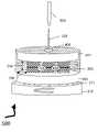
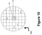
- FIG. 10illustrates a top view of the coupled wafer pair 900 having a plurality of dice 1001 and a gap fill, in accordance with an embodiment of the present invention.
- top view as shown in FIG. 10is the first wafer 901 of the coupled wafer pair 900 .
- coupled wafer paircontains a plurality of the dice 1001 having integrated circuits that are sliced and diced from the coupled wafer pair 900 into single stack chip die.
- FIG. 10also illustrates the hole 406 in the coupled wafer pair 900 that fills the center gap 108 with the material 208 .
- the material 208also fills the outer gap 106 between the coupled wafer pair 900 as shown in FIG. 9B .
- the material 208is applied into a gap between the coupled wafer pair 900 as described with reference to FIGS. 2A–9B . In one embodiment of the present invention, the material 208 is cured after injection and prior to cutting and/or grinding.
- FIG. 11illustrates a die 1001 that is cut from the coupled waferpair 900 having a gap fill, in accordance with an embodiment of the present invention.
- the die 1001is one of a plurality of dice as illustrated with FIG. 10 .
- the die 1001is a single stack chip die.
- a substrate 1101is connected to a substrate 1102 through in the interconnect layer 203 .
- the material 208fills the region having gaps in between the substrates 1101 and 1102 .
- a copper vias 1103 in the substrate 1102connect the die 1001 to a solder bumps 1104 .
- the solder bumps 1104connect the die 1001 to a packaging layer of an integrated circuit.
- the die 1001is a three-dimensional integrated circuit device having a first integrated circuit and a second integrated circuit.
- the die 1001is a three-dimensional integrated circuit device having a first integrated circuit and a second integrated circuit that are parts of a single microprocessor.
- the die 1001is a stacked chipset.
- a material 203is polymer foam.
- the material 208is cured after injection and prior to cutting and/or grinding.
- the material 203is similar to the material as described with reference to FIGS. 2A–2B .
Landscapes
- Engineering & Computer Science (AREA)
- Microelectronics & Electronic Packaging (AREA)
- Physics & Mathematics (AREA)
- Condensed Matter Physics & Semiconductors (AREA)
- General Physics & Mathematics (AREA)
- Computer Hardware Design (AREA)
- Power Engineering (AREA)
- Manufacturing & Machinery (AREA)
- Mechanical Treatment Of Semiconductor (AREA)
- Internal Circuitry In Semiconductor Integrated Circuit Devices (AREA)
Abstract
Description
1. Field of the Invention
The present invention relates to the field of three dimensional integrated circuits and more specifically, to a method for forming a coupled wafer pair that prevents edge chipping.
2. Discussion of Related Art
In the manufacture of microelectronic devices, packaging density is becoming increasingly important. Stacking of the dice of a multi-processor microelectronic device is one way to improve the packaging density of a microelectronic device. Stacked microelectronic devices are typically formed by electrically connecting two or more wafers through interconnect layers, and then dicing the stacked wafers into individual stacked devices.
Next, as shown inFIG. 1C , thefirst wafer 101 and its associatedinterconnect layer 103 is flipped around and positioned over thesecond wafer 102 and itsinterconnect layer 103. Next, inFIG. 1D , a coupledwafer pair 100 is formed by aligning theinterconnect layers 103 of thefirst wafer 101 and thesecond wafer 102 and bringing thefirst wafer 101 and thesecond wafer 102 together. Typically a thermo-compression process is used to couple thefirst wafer 101 with thesecond wafer 102.
Typically, as shown inFIG. 1D , thinning107 of one of the stacked wafers is performed by use of one or more mechanical and/or chemical processes such as a polishing process for example. These processes may cause mechanical stresses in unsupported portions of the wafer being thinned. As shown in anouter gap 106, an area formed by the product of adepth 105 and aheight 104 is unsupported by theinterconnect layer 103. Furthermore, acenter gap 108 between individual members of theinterconnect layer 103 may also be unsupported.
Embodiments of the present invention are three dimensional integrated circuit devices having a gap fill and their methods of formation. In the following description numerous specific details have been set forth in order to provide a thorough understanding of the present invention. In other instances, well-known semiconductor fabrication processes and techniques have not been set forth in particular detail in order to avoid unnecessarily obscuring the present invention.
Embodiments of the present invention are a method for applying a material on a coupled wafer pair in order to fill a gap between wafers of the coupled wafer pair. Embodiments of the invention include applying a material through a hole within one of the wafers of the coupled wafer pair and creating a pressure differential to help the material flow between the coupled wafers. Embodiments of the invention include spinning a coupled wafer pair, applying a material on the top of or directly in a gap between the coupled wafer pair, and using a vacuum to create a pressure differential between the coupled wafers. The advantages of the present invention include protecting gaps between a coupled wafer pair from chipping, cracking, corroding, or other damage which may result in the wafer and/or individual stacked devices being unusable.
An example of a method for applying a material on top of afirst wafer 201 of a coupledwafer pair 200 in accordance with an embodiment of the present invention is illustrated inFIGS. 2A–2B . In one embodiment of the present invention, the coupled wafer pair is formed similarly as described with reference toFIGS. 1A–1D . In one embodiment of the present invention, there are more than two wafers that are coupled together. The coupledwafer pair 200 is placed over achuck 210 having a plurality ofvacuum ports 211. In one embodiment of the present invention, thevacuum ports 211 generate a vacuum to secure the coupledwafer pair 200 to thechuck 210.
Next, thechuck 210 and the coupledwafer pair 200 are spun around at a first spin speed. In one embodiment of the present invention, the first spin speed is approximately 500–3,000 rotations per minute. In one embodiment of the present invention, the first spin speed is performed at a rate of at least 1000 rpm for approximately 20 seconds if thefirst wafer 201 and asecond wafer 202 are 300 mm in diameter.
Next, as shown inFIG. 2B , anapplicator 209 applies amaterial 208 on top of the coupledwafer 200. In one embodiment of the present invention, thematerial 208 is applied at the center over the top of thewafer 201. In another embodiment of the present invention, thematerial 208 is applied anywhere on top of thewafer 201. In one embodiment theapplicator 209 is a syringe. In another embodiment of the present invention, theapplicator 209 is a dispenser nozzle. In one embodiment of the present invention, anapplicator 219, instead of theapplicator 209, applies thematerial 208 on the top edge of the coupledwafer 200. In one embodiment of the present invention, thematerial 208 covers the bevel of the coupledwafer pair 200. In one embodiment of the present invention, thematerial 208 covers the edge bead removal region of the coupled wafer pair. In one embodiment of the present invention, thematerial 208 covers a depth necessary to prevent the coupledwafer pair 200 from cracking when it is later grinded. In one embodiment of the present invention, thematerial 208 covers a depth necessary to prevent aninterconnect layer 203 from corroding.
In one embodiment of the present invention, a low viscosity polymer is preferred for thematerial 208 when aheight 204 between the coupledwafers outer gap 106, formed by the product of theheight 204 and adepth 205. In one embodiment of the present invention, the gap between the coupledwafers height 204. In one embodiment of the present invention, a high viscosity polymer material is preferred for thematerial 208. A high viscosity polymer is preferred when theheight 204 between the coupledwafers wafer pair 200. In one embodiment of the present invention, when theheight 204 between the coupledwafers
In one embodiment of the present invention, the high viscosity and low viscosity polymer material is selected from a group consisting of SiLK-J, polyimide, spin-on glass, benzocyclobutene, polynorbornene, and polyarylenes. In one embodiment of the present invention, thematerial 208 has a viscosity of less than 1,000 centipoise when theheight 204 is less than 1 micron. In another embodiment when theheight 204 is greater than 5 microns, thematerial 208 has a viscosity of greater than 1,000 centipoise. In one embodiment of the present invention, the coupledwafer pair 200 are coupled wafers that are coupled through theinterconnect layer 203.
Next, the coupledwafer 200 is spun at a second spin speed after theapplicator 209 finishes dispensing thematerial 208. In one embodiment of the present invention, this second spin speed is approximately 0–50 rotations per minute. Because the second spin speed is so much less than the first spin speed, thematerial 208 is wicked around the edge of thefirst wafer 201 as a result of capillary forces. The material208 then fills theouter gap 106, formed by the product of thedepth 205 and theheight 204 in the coupledwafer pair 200. In one embodiment of the present invention, the second spin speed is performed at a deceleration rate of approximately 5,000–10,000 rotations per minute.
In one embodiment of the present invention, thematerial 208 is cured (e.g., thematerial 208 is cured to harden it after it is applied). For instance, thematerial 208 may be cured using a polymerization technique. Alternatively, thematerial 208 may be cured using thermal curing or UV curing. In one embodiment of the present invention, curing holds the coupledwafer pair 200 between 75–150 C for 1 hour in air or nitrogen for epoxy type materials. In another embodiment of the present invention, curing holds the coupledwafer pair 200 between 200–400 C for 1 hour in nitrogen for spin-on polymer materials. In one embodiment of the present invention, curing is performed by epoxy materials that harden without heat (e.g., cross-linking agent is added to a polymer).
In one embodiment of the present invention, the coupledwafer 200 is spun at a third spin speed to clear theexcessive material 208. In one embodiment of the present invention, the third spin speed is the same as the first spin speed. In one embodiment of the present invention, the coupledwafer pair 200 is ground down to a thickness of approximately 10–50 microns after thematerial 208 is applied.
Next, thechuck 210 and the coupledwafer pair 300 are spun around at a first spin speed. In one embodiment of the present invention, the first spin speed is approximately 500–3,000 rotations per minute.
Next, as shown inFIG. 3B , anapplicator 309 applies the material208 directly into theouter gap 106 in the coupledwafer pair 300. Applying thematerial 208 directly between theouter gap 106 prevents later cleanup of material on the top of a wafer, as required inFIG. 2 . Furthermore, applying thematerial 208 directly between theouter gap 106 minimizes the quantity of the material208 that must be used because material is not wasted on the top of a wafer.
In one embodiment of the present invention, theapplicator 309 applies the material208 at a 90 degree angle to the coupledwafer pair 300. In one embodiment of the present invention, theapplicator 309 applies a material horizontally, directly into theouter gap 106 between the coupledwafer pair 300. In one embodiment of the present invention, theapplicator 309 is brought into thecenter gap 108 before applying thematerial 208. In one embodiment of the present invention, theapplicator 309 applies material at an angle less than 90 degrees to the coupledwafer pair 300. The coupledwafer pair 300 is spun on thechuck 210 while theapplicator 309 applies material directly into theouter gap 106. This causes the entireouter gap 106 to be filled by thematerial 208. In one embodiment of the present invention, theapplicator 309 is a syringe. In another embodiment of the present invention, theapplicator 309 is a dispenser nozzle. In one embodiment of the present invention, thematerial 208 is cured after injection and prior to cutting and/or grinding.
In one embodiment of the present invention, a low viscosity polymer material is preferred for thematerial 208. A low viscosity polymer is preferred when theheight 204 between the coupledwafers outer gap 106 formed by the product of theheight 204 and thedepth 205. In another embodiment of the present invention, a high viscosity polymer material is preferred for thematerial 208. A high viscosity polymer is preferred when theheight 204 between the coupledwafers wafer pair 300 because of its greater thickness. In one embodiment of the present invention, when theheight 204 between the coupledwafers FIGS. 3A and 3B are similar to those described in detail with reference toFIGS. 2A–2B .
In one embodiment of the present invention, the hole is the size of a dummified region on the coupledwafer pair 400. The dummified region does not contain any integrated circuits but only contains blank die. Thehole 406 should preferably be as small as possible, in one embodiment of the present invention, in order to maximize die yield on the coupledwafer pair 400. By limiting thehole 406 to a dummified region on thefirst wafer 401, die yield impact is not impacted significantly. In one embodiment of the present invention, thehole 406 is approximately 1 millimeter or larger in order to maximize the amount of the material208 that passes through thehole 406 and the coupledwafer pair 400. In one embodiment of the present invention, the hole may be created on thefirst wafer 401 and on thesecond wafer 202. In one embodiment of the present invention, multiple holes may be created on various locations of thefirst wafer 401. In one embodiment of the present invention, thehole 406 may be created on thesecond wafer 202.
Next, the coupledwafer pair 400 is placed on thechuck 210. The coupledwafer pair 400 is held on thechuck 210 through thevacuum 211 that is applied on the coupledwafer pair 400 to hold the coupledwafer pair 400 in place. UnlikeFIG. 2B andFIG. 3B , the coupledwafer pair 400 and thechuck 210 are not spun in one embodiment of the present invention, as illustrated inFIG. 4B .
Next, thematerial 208 is applied by anapplicator 409 through thehole 406 in thefirst wafer 401. In one embodiment of the present invention, theapplicator 409 is the same applicator as theapplicator 209 described with reference toFIG. 2B . By applying thematerial 208 directly into the center of the coupledwafer pair 400 through thehole 406, thecenter gap 108 between members of theinterconnect layer 203 are supported. In addition, by applying thematerial 208 directly into the center of the coupledwafer pair 400, theinterconnect layer 203 does not corrode and individual devices that are cut from the coupledwafer pair 400 are better supported. In one embodiment of the present invention, thematerial 208 may also flow to theouter gap 106 in addition to thecenter gap 108 of the coupledwafer pair 400. In one embodiment of the present invention, theapplicator 409 is a syringe. In another embodiment of the present invention, theapplicator 409 is a dispenser nozzle. In one embodiment of the present invention, thematerial 208 is cured after injection and prior to cutting and/or grinding.
In one embodiment of the present invention, when theheight 204 between the coupledwafers material 208 has a viscosity of less than 1,000 centipoise when theheight 204 is less than 1 micron. In another embodiment when theheight 204 is greater than 5 microns, thematerial 208 has a viscosity of greater than 1,000 centipoise. In one embodiment of the present invention, the gap between the coupledwafers height 204. In one embodiment of the present invention, the coupledwafer pair 400 is ground down to a thickness of approximately 10–50 microns after thematerial 208 is applied. Other embodiments of the present invention as shown inFIGS. 4A and 4B are similar to those described with reference toFIGS. 2A and 2B .
Next, in602, a pressure differential is created between thehole 406 in at least one of the coupled wafers and thecenter gap 108 and theouter gap 106 between the coupled wafer pair. In one embodiment of the present invention, a vacuum creates a pressure differential between thehole 406 and theouter gap 106. In one embodiment of the present invention, a vacuum is applied directly into thehole 406 and thematerial 208 is applied at the gap. In one embodiment of the present invention, a vacuum is applied directly into a gap between the coupledwafer pair 400 and thematerial 208 is applied at thehole 406. This embodiment switches the place of the vacuum and the applicator and may provide preferred characteristics for the diffusion of the material208 in some embodiments of the present invention. In one embodiment of the present invention, a positive pressure is applied at theouter gap 106 in addition to anapplicator 509 to increase the diffusion of the material208 toward thecenter gap 108 of coupled wafer pair.
In603, thematerial 208 fills theouter gap 106 and thecenter gap 108 by spreading through the coupled wafers because of the pressure differential. In one embodiment of the present invention, thematerial 208 is applied similarly as described with reference toFIGS. 3A–3B . In one embodiment of the present invention, thematerial 208 is drawn toward thehole 406 through the application of a vacuum as described with reference to602. In one embodiment of the present invention, a high viscosity or a low viscosity polymer is used for thematerial 208 depending on theheight 204, as described with reference toFIGS. 3A–3B . In one embodiment of the invention, a pressure differential is created by a vacuum applied at thehole 406 and a positive pressure applied at theouter gap 106. In one embodiment of the present invention, thematerial 208 is cured after injection and prior to cutting and/or grinding.
In addition, various embodiments of the present invention can be used to create thehole 406 as described with reference toFIGS. 4A–4B . In addition, thevacuum 750 is applied during the application of thematerial 208. As such, thematerial 208 moves from theouter gap 106 toward thecenter gap 108 of the coupledwafer pair 700 because of the pressure differential created by thevacuum 750. In one embodiment of the present invention, thevacuum 750 is applied directly into a gap between the coupledwafer pair 700 and thematerial 208 is applied at thehole 406. This embodiment switches the place of thevacuum 750 and theapplicator 709 and may provide preferred characteristics for the diffusion of the material208 in some embodiments of the present invention. In one embodiment of the present invention, a positive pressure is applied at theouter gap 106 in addition to theapplicator 709 to increase the diffusion of the material208 toward thecenter gap 108 of the coupledwafer pair 700. In one embodiment of the present invention, thematerial 208 is cured after injection and prior to cutting and/or grinding. Other embodiments of the present invention as shown inFIGS. 7A and 7B are similar to those described with reference toFIGS. 2A–2B ,FIGS. 4A–4B , andFIGS. 5A–5B .
It should be noted that the embodiments disclosed herein may be applied to the formation of any stacked microelectronic device. Certain features of the embodiments of the claimed subject matter have been illustrated as described herein, however, may modifications, substitutions, changes and equivalents will be evident to those skilled in the art. Additionally, while several functional blocks and relationships have been described in detail, it is contemplated by those of skill in the art that several of the operations may be performed without the use of the others, or additional functions or relationships between operations may be established and still remain in accordance with the claimed subject matter. It is, therefore, to be understood that the appended claims are intended to cover all such modifications and changes as fall within the true spirit of the claimed subject matter.
Claims (63)
1. A process, comprising:
spinning a first wafer bonded to a second wafer at a first spin speed, said first wafer positioned above said second wafer to form a gap between said bonded first and second wafers; and
applying a material on a top surface of said first wafer until said material flows to an edge of said first wafer enabling said material to flow into said gap between said bonded first and second wafers.
2. The process ofclaim 1 , further comprising:
spinning said first wafer bonded to said second wafer at a second spin speed to a point where said material flows from said edge of said first wafer to fill said gap between said first wafer and said second wafer; and
curing said material.
3. The process ofclaim 2 , further comprising:
spinning said first wafer bonded to said second wafer at a third spin speed to clear excessive said material.
4. The process ofclaim 3 , further comprising:
grinding down said first wafer to a thickness of approximately 10–50 microns.
5. The process ofclaim 1 , wherein said gap is less than 1 micron in height, and said material is a low viscosity polymer material from a group consisting of SiLK-J, polyimide, spin-on glass, benzocyclobutene, polynorbornene, and polyarylenes.
6. The process ofclaim 1 , wherein said gap is greater than 5 microns in height, and said material is a high viscosity polymer material from a group consisting of SiLK-J, polyimide, spin-on glass, benzocyclobutene, polynorbornene, and polyarylenes.
7. The process ofclaim 5 , wherein said material has a viscosity of less than 1000 centipoise.
8. The process ofclaim 6 , wherein said material has a viscosity of greater than 1000 centipoise.
9. The process ofclaim 1 , wherein said gap is at least 250 microns in depth and at most 300 microns in height.
10. The process ofclaim 2 , wherein said second spin speed is performed at a deceleration rate of approximately 5,000 to 10,000 rpm/second.
11. The process ofclaim 1 , wherein said applying a material is at a center of the top of said first wafer.
12. The process ofclaim 3 , wherein said third spin speed is faster than said second spin speed.
13. The process ofclaim 3 , wherein said first spin speed is approximately 500 to 3,000 rpm.
14. The process ofclaim 13 , wherein said first spin speed and said third spin speed are the same.
15. The process ofclaim 13 , wherein said second speed is approximately 0 to 50 rpm.
16. The process ofclaim 13 , wherein said material is applied directly into said gap between said first wafer and said second wafer.
17. A process, comprising:
creating a hole in a center of a first wafer;
bonding said first wafer to a second wafer to create a bonded wafer pair;
applying a polymer material through said hole to cause said material to flow through said hole and into a gap between said bonded wafer pair; and
curing said material.
18. The process ofclaim 17 , further comprising:
spinning said bonded wafer pair while applying said material.
19. The process ofclaim 18 , further comprising:
reducing spin speed of spinning suddenly to fill a gap between said bonded wafers after applying said material.
20. The process ofclaim 19 , further comprising:
increasing spin speed of spinning said bonded wafer pair to clear excessive said material.
21. The process ofclaim 17 , in which said material also flows to the edge of said first wafer.
22. The process ofclaim 17 , in which creating said hole is created using approximately a ¼ to 1/16 inch hollow core drill bit having a diamond coating on it to make an approximately ¼ to 1/16 inch hole in diameter.
23. The process ofclaim 22 , in which creating said hole is performed before said bonding.
24. The process ofclaim 17 , in which creating said hole is created using approximately 5 to 15 second laser pulsing.
25. The process ofclaim 17 , in which creating said hole is created using an ion beam.
26. The process ofclaim 17 , in which said hole is a size of a dummified region on said bonded wafer pair.
27. The process ofclaim 17 , in which said hole is approximately 1 millimeter or larger.
28. The process ofclaim 17 , in which a plurality of holes is created in said first wafer.
29. A wafer coupling method, comprising:
spinning a set of coupled wafers;
creating a pressure differential between a hole in at least one of the coupled wafers and a gap between the coupled wafers;
causing a material to fill said gap by spreading said material through said coupled wafers because of said pressure differential; and
curing said material.
30. The method ofclaim 29 , in which a vacuum creates said pressure differential between said hole and said gap.
31. The method ofclaim 30 , in which said vacuum is applied directly at said hole, and said material is applied directly at said gap.
32. The method ofclaim 30 , in which said vacuum is applied directly at said gap, and said material is applied directly at said hole.
33. The method ofclaim 32 , further comprising:
applying a positive pressure at said hole to push said material through said hole.
34. The method ofclaim 29 , further comprising:
grinding down at least one of said coupled wafers to a thickness of approximately 10–50 microns.
35. The method ofclaim 29 , wherein said gap is less than 1 micron in height, and said material is a low viscosity polymer material from a group consisting of SiLK-J, polyimide, spin-on glass, benzocyclobutene, polynorbornene, and polyarylenes.
36. The method ofclaim 29 , wherein said gap is greater than 5 microns in height, and said material is a high viscosity polymer material from a group consisting of SiLK-J, polyimide, spin-on glass, benzocyclobutene, polynorbornene, and polyarylenes.
37. The method ofclaim 35 , wherein said material has a viscosity of less than 1000 centipoise.
38. The method ofclaim 36 , wherein said material has a viscosity of greater than 1000 centipoise.
39. A wafer coupling method, comprising:
creating a hole in a center of a first wafer;
coupling said first wafer to a second wafer to create a coupled wafer pair;
spinning said coupled wafer pair;
applying a vacuum at said hole;
applying a material directly into a gap between said coupled wafer pair;
attracting said material toward said hole of said coupled wafer pair through said gap by applying said vacuum at said hole; and
curing said material.
40. The method ofclaim 39 , in which said vacuum creates a pressure differential between said hole and said gap.
41. The method ofclaim 39 , further comprising:
grinding down said first wafer to a thickness of approximately 10–50 microns.
42. The method ofclaim 39 , wherein said gap is less than 1 micron in height, and said material is a low viscosity polymer material from a group consisting of SiLK-J, polyimide, spin-on glass, benzocyclobutene, polynorbornene, and polyarylenes.
43. The method ofclaim 39 , wherein said gap is greater than 5 microns in height, and said material is a high viscosity polymer material from a group consisting of SiLK-J, polyimide, spin-on glass, benzocyclobutene, polynorbornene, and polyarylenes.
44. The method ofclaim 42 , wherein said material has a viscosity of less than 1000 centipoise.
45. The method ofclaim 43 , wherein said material has a viscosity of greater than 1000 centipoise.
46. The method ofclaim 39 , in which a plurality of holes is created in said first wafer.
47. The method ofclaim 39 , in which said hole is created prior to coupling said first wafer to said second wafer.
48. A wafer coupling method, comprising:
coupling a first wafer to a second wafer to create a coupled wafer pair;
spinning said coupled wafer pair;
applying a vacuum directly in a gap between said coupled wafer pair;
applying a material on top of said coupled wafer pair causing said material to flow through a hole through said first wafer of said coupled wafer pair;
attracting said material toward said gap by creating a pressure differential between said hole and said gap; and
curing said material.
49. The method ofclaim 48 , further comprising:
creating said hole through said first wafer in a center of said first wafer prior to coupling said first wafer to said second wafer.
50. The method ofclaim 48 , further comprising:
grinding down said first wafer to a thickness of approximately 10–50 microns.
51. The method ofclaim 48 , wherein said gap is less than 1 micron in height, and said material is a low viscosity polymer material from a group consisting of SiLK-J, polyimide, spin-on glass, benzocyclobutene, polynorbornene, and polyarylenes.
52. The method ofclaim 48 , wherein said gap is greater than 5 microns in height, and said material is a high viscosity polymer material from a group consisting of SiLK-J, polyimide, spin-on glass, benzocyclobutene, polynorbornene, and polyarylenes.
53. The method ofclaim 51 , wherein said material has a viscosity of less than 1000 centipoise.
54. The method ofclaim 52 , wherein said material has a viscosity of greater than 1000 centipoise.
55. The method ofclaim 48 , in which a plurality of holes is created in said first wafer.
56. The method ofclaim 48 , further comprising:
applying a positive pressure at said hole to push said material through said hole.
57. A three-dimensional (3-D) integrated chip system, comprising:
a first wafer having a hole in a center of said first wafer;
a second wafer that is bonded to said first wafer, creating a bonded wafer pair; and
a material within a gap created when said bonded wafer pair is created, said gap between said first wafer and said second wafer in said bonded wafer pair.
58. The system ofclaim 57 , wherein
said first wafer is grounded down to a thickness of approximately 10–50 microns after curing said material.
59. The system ofclaim 57 , wherein said gap is less than 1 micron in height, and said material is a low viscosity polymer material from a group consisting of SiLK-J, polyimide, spin-on glass, benzocyclobutene, polynorbornene, and polyarylenes.
60. The system ofclaim 57 , wherein said gap is greater than 5 microns in height, and said material is a high viscosity polymer material from a group consisting of SiLK-J, polyimide, spin-on glass, benzocyclobutene, polynorbornene, and polyarylenes.
61. The system ofclaim 59 , wherein said material has a viscosity of less than 1000 centipoise.
62. The system ofclaim 60 , wherein said material has a viscosity of greater than 1000 centipoise.
63. The system ofclaim 57 , wherein at least two holes is created in said first wafer.
Priority Applications (1)
| Application Number | Priority Date | Filing Date | Title |
|---|---|---|---|
| US10/919,550US7087538B2 (en) | 2004-08-16 | 2004-08-16 | Method to fill the gap between coupled wafers |
Applications Claiming Priority (1)
| Application Number | Priority Date | Filing Date | Title |
|---|---|---|---|
| US10/919,550US7087538B2 (en) | 2004-08-16 | 2004-08-16 | Method to fill the gap between coupled wafers |
Publications (2)
| Publication Number | Publication Date |
|---|---|
| US20060035476A1 US20060035476A1 (en) | 2006-02-16 |
| US7087538B2true US7087538B2 (en) | 2006-08-08 |
Family
ID=35800524
Family Applications (1)
| Application Number | Title | Priority Date | Filing Date |
|---|---|---|---|
| US10/919,550Expired - LifetimeUS7087538B2 (en) | 2004-08-16 | 2004-08-16 | Method to fill the gap between coupled wafers |
Country Status (1)
| Country | Link |
|---|---|
| US (1) | US7087538B2 (en) |
Cited By (109)
| Publication number | Priority date | Publication date | Assignee | Title |
|---|---|---|---|---|
| US20070111386A1 (en)* | 2002-02-20 | 2007-05-17 | Kim Sarah E | Process of vertically stacking multiple wafers supporting different active integrated circuit (IC) devices |
| US20080268614A1 (en)* | 2007-04-25 | 2008-10-30 | Ku-Feng Yang | Wafer Bonding |
| US20080274592A1 (en)* | 2007-05-04 | 2008-11-06 | Chien-Hsiun Lee | Process and apparatus for wafer-level flip-chip assembly |
| US20090091041A1 (en)* | 2007-10-05 | 2009-04-09 | Advanced Semiconductor Engineering, Inc. | Stacked type chip package structure and method of fabricating the same |
| US20090130840A1 (en)* | 2007-11-16 | 2009-05-21 | Chung Yu Wang | Protected Solder Ball Joints in Wafer Level Chip-Scale Packaging |
| US20100248427A1 (en)* | 2009-03-27 | 2010-09-30 | Taiwan Semiconductor Manufacturing Company, Ltd. | Method of handling a thin wafer |
| US20110027944A1 (en)* | 2009-07-30 | 2011-02-03 | Taiwan Semiconductor Maufacturing Company, Ltd. | Method of forming electrical connections |
| US20110058346A1 (en)* | 2008-07-21 | 2011-03-10 | Taiwan Semiconductor Manufacturing Company, Ltd. | Bonding Metallurgy for Three-Dimensional Interconnect |
| US20110062592A1 (en)* | 2009-09-11 | 2011-03-17 | Taiwan Semiconductor Manufacturing Company, Ltd. | Delamination Resistance of Stacked Dies in Die Saw |
| US20110091685A1 (en)* | 2009-10-21 | 2011-04-21 | International Business Machines Corporation | Polymeric edge seal for bonded substrates |
| US20110104426A1 (en)* | 2009-10-29 | 2011-05-05 | International Business Machines Corporation | Edge protection seal for bonded substrates |
| US20110186986A1 (en)* | 2010-01-29 | 2011-08-04 | Taiwan Semiconductor Manufacturing Company, Ltd. | T-Shaped Post for Semiconductor Devices |
| US20110186967A1 (en)* | 2008-12-05 | 2011-08-04 | Taiwan Semiconductor Manufacturing Company, Ltd. | Component Stacking Using Pre-Formed Adhesive Films |
| US20110193221A1 (en)* | 2010-02-05 | 2011-08-11 | Taiwan Semiconductor Manufacturing Company, Ltd. | 3DIC Architecture with Interposer for Bonding Dies |
| US20110193219A1 (en)* | 2010-02-09 | 2011-08-11 | Taiwan Seimconductor Manufacturing Company, Ltd. | Semiconductor device and semiconductor assembly with lead-free solder |
| US20110210444A1 (en)* | 2010-02-26 | 2011-09-01 | Taiwan Semiconductor Manufacturing Company, Ltd. | 3D Semiconductor Package Using An Interposer |
| US20110215470A1 (en)* | 2010-03-04 | 2011-09-08 | Taiwan Semiconductor Manufacturing Company, Ltd. | Dummy Wafers in 3DIC Package Assemblies |
| US20110233761A1 (en)* | 2009-07-30 | 2011-09-29 | Taiwan Semiconductor Manufacturing Company, Ltd. | Cu pillar bump with non-metal sidewall protection structure |
| US8241963B2 (en) | 2010-07-13 | 2012-08-14 | Taiwan Semiconductor Manufacturing Company, Ltd. | Recessed pillar structure |
| US8319349B2 (en) | 2010-10-14 | 2012-11-27 | Taiwan Semiconductor Manufacturing Company, Ltd. | Approach for bonding dies onto interposers |
| US8324738B2 (en) | 2009-09-01 | 2012-12-04 | Taiwan Semiconductor Manufacturing Company, Ltd. | Self-aligned protection layer for copper post structure |
| US8334170B2 (en) | 2008-06-27 | 2012-12-18 | Taiwan Semiconductor Manufacturing Company, Ltd. | Method for stacking devices |
| US8338945B2 (en) | 2010-10-26 | 2012-12-25 | Taiwan Semiconductor Manufacturing Company, Ltd. | Molded chip interposer structure and methods |
| US20130075365A1 (en)* | 2010-05-21 | 2013-03-28 | Commissariat A L'energie Atomique Et Aux Energies Alternatives | Method for building a substrate holder |
| US8426961B2 (en) | 2010-06-25 | 2013-04-23 | Taiwan Semiconductor Manufacturing Company, Ltd. | Embedded 3D interposer structure |
| US8441124B2 (en) | 2010-04-29 | 2013-05-14 | Taiwan Semiconductor Manufacturing Company, Ltd. | Cu pillar bump with non-metal sidewall protection structure |
| US8455995B2 (en) | 2010-04-16 | 2013-06-04 | Taiwan Semiconductor Manufacturing Company, Ltd. | TSVs with different sizes in interposers for bonding dies |
| US8501590B2 (en) | 2011-07-05 | 2013-08-06 | Taiwan Semiconductor Manufacturing Company, Ltd. | Apparatus and methods for dicing interposer assembly |
| US8518796B2 (en) | 2012-01-09 | 2013-08-27 | Taiwan Semiconductor Manufacturing Company, Ltd. | Semiconductor die connection system and method |
| US8518753B2 (en) | 2011-11-15 | 2013-08-27 | Taiwan Semiconductor Manufacturing Company, Ltd. | Assembly method for three dimensional integrated circuit |
| US8531032B2 (en) | 2011-09-02 | 2013-09-10 | Taiwan Semiconductor Manufacturing Company, Ltd. | Thermally enhanced structure for multi-chip device |
| US8536573B2 (en) | 2011-12-02 | 2013-09-17 | Taiwan Semiconductor Manufacturing Company, Ltd. | Plating process and structure |
| US8540506B2 (en) | 2010-08-16 | 2013-09-24 | Taiwan Semiconductor Manufacturing Company, Ltd. | Semiconductor molding chamber |
| US8546254B2 (en) | 2010-08-19 | 2013-10-01 | Taiwan Semiconductor Manufacturing Company, Ltd. | Mechanisms for forming copper pillar bumps using patterned anodes |
| US8546945B2 (en) | 2010-02-11 | 2013-10-01 | Taiwan Semiconductor Manufacturing Company, Ltd. | Pillar structure having a non-planar surface for semiconductor devices |
| US8557631B2 (en) | 2011-12-01 | 2013-10-15 | Taiwan Semiconductor Manufacturing Co., Ltd. | Interposer wafer bonding method and apparatus |
| US8557684B2 (en) | 2011-08-23 | 2013-10-15 | Taiwan Semiconductor Manufacturing Company, Ltd. | Three-dimensional integrated circuit (3DIC) formation process |
| US8558229B2 (en) | 2011-12-07 | 2013-10-15 | Taiwan Semiconductor Manufacturing Company, Ltd. | Passivation layer for packaged chip |
| US8569086B2 (en) | 2011-08-24 | 2013-10-29 | Taiwan Semiconductor Manufacturing Company, Ltd. | Semiconductor device and method of dicing semiconductor devices |
| US8581418B2 (en) | 2010-07-21 | 2013-11-12 | Taiwan Semiconductor Manufacturing Company, Ltd. | Multi-die stacking using bumps with different sizes |
| US8580683B2 (en) | 2011-09-27 | 2013-11-12 | Taiwan Semiconductor Manufacturing Company, Ltd. | Apparatus and methods for molding die on wafer interposers |
| US8610285B2 (en) | 2011-05-30 | 2013-12-17 | Taiwan Semiconductor Manufacturing Company, Ltd. | 3D IC packaging structures and methods with a metal pillar |
| US8629568B2 (en) | 2010-07-30 | 2014-01-14 | Taiwan Semiconductor Manufacturing Company, Ltd. | Semiconductor device cover mark |
| US8629043B2 (en) | 2011-11-16 | 2014-01-14 | Taiwan Semiconductor Manufacturing Company, Ltd. | Methods for de-bonding carriers |
| US8628990B1 (en) | 2012-09-27 | 2014-01-14 | Taiwan Semiconductor Manufacturing Company, Ltd. | Image device and methods of forming the same |
| US8643148B2 (en) | 2011-11-30 | 2014-02-04 | Taiwan Semiconductor Manufacturing Company, Ltd. | Chip-on-Wafer structures and methods for forming the same |
| US8647796B2 (en) | 2011-07-27 | 2014-02-11 | Taiwan Semiconductor Manufacturing Company, Ltd. | Photoactive compound gradient photoresist |
| US8653658B2 (en) | 2011-11-30 | 2014-02-18 | Taiwan Semiconductor Manufacturing Company, Ltd. | Planarized bumps for underfill control |
| US8659155B2 (en) | 2009-11-05 | 2014-02-25 | Taiwan Semiconductor Manufacturing Company, Ltd. | Mechanisms for forming copper pillar bumps |
| US8664760B2 (en) | 2011-05-30 | 2014-03-04 | Taiwan Semiconductor Manufacturing Company, Ltd. | Connector design for packaging integrated circuits |
| US8691706B2 (en) | 2012-01-12 | 2014-04-08 | Taiwan Semiconductor Manufacturing Company, Ltd. | Reducing substrate warpage in semiconductor processing |
| US8698308B2 (en) | 2012-01-31 | 2014-04-15 | Taiwan Semiconductor Manufacturing Company, Ltd. | Bump structural designs to minimize package defects |
| US8716867B2 (en) | 2010-05-12 | 2014-05-06 | Taiwan Semiconductor Manufacturing Company, Ltd. | Forming interconnect structures using pre-ink-printed sheets |
| US8741691B2 (en) | 2012-04-20 | 2014-06-03 | Taiwan Semiconductor Manufacturing Company, Ltd. | Method of fabricating three dimensional integrated circuit |
| US8754514B2 (en) | 2011-08-10 | 2014-06-17 | Taiwan Semiconductor Manufacturing Company, Ltd. | Multi-chip wafer level package |
| US8759118B2 (en) | 2011-11-16 | 2014-06-24 | Taiwan Semiconductor Manufacturing Company, Ltd. | Plating process and structure |
| US8772929B2 (en) | 2011-11-16 | 2014-07-08 | Taiwan Semiconductor Manufacturing Company, Ltd. | Package for three dimensional integrated circuit |
| US8779599B2 (en) | 2011-11-16 | 2014-07-15 | Taiwan Semiconductor Manufacturing Company, Ltd. | Packages including active dies and dummy dies and methods for forming the same |
| US8779588B2 (en) | 2011-11-29 | 2014-07-15 | Taiwan Semiconductor Manufacturing Company, Ltd. | Bump structures for multi-chip packaging |
| US8797057B2 (en) | 2011-02-11 | 2014-08-05 | Taiwan Semiconductor Manufacturing Company, Ltd. | Testing of semiconductor chips with microbumps |
| US8803319B2 (en) | 2010-02-11 | 2014-08-12 | Taiwan Semiconductor Manufacturing Company, Ltd. | Pillar structure having a non-planar surface for semiconductor devices |
| US8816495B2 (en) | 2012-02-16 | 2014-08-26 | Taiwan Semiconductor Manufacturing Company, Ltd. | Structures and formation methods of packages with heat sinks |
| US8828848B2 (en) | 2011-12-16 | 2014-09-09 | Taiwan Semiconductor Manufacturing Company, Ltd. | Die structure and method of fabrication thereof |
| US8871568B2 (en) | 2012-01-06 | 2014-10-28 | Taiwan Semiconductor Manufacturing Company, Ltd. | Packages and method of forming the same |
| US8878182B2 (en) | 2011-10-12 | 2014-11-04 | Taiwan Semiconductor Manufacturing Company, Ltd. | Probe pad design for 3DIC package yield analysis |
| US8901736B2 (en) | 2010-05-28 | 2014-12-02 | Taiwan Semiconductor Manufacturing Company, Ltd. | Strength of micro-bump joints |
| US8932906B2 (en) | 2008-08-19 | 2015-01-13 | Taiwan Semiconductor Manufacturing Company, Ltd. | Through silicon via bonding structure |
| US8936966B2 (en) | 2012-02-08 | 2015-01-20 | Taiwan Semiconductor Manufacturing Company, Ltd. | Packaging methods for semiconductor devices |
| US8953336B2 (en) | 2012-03-06 | 2015-02-10 | Taiwan Semiconductor Manufacturing Co., Ltd. | Surface metal wiring structure for an IC substrate |
| US8962392B2 (en) | 2012-03-13 | 2015-02-24 | Taiwan Semiconductor Manufacturing Company, Ltd. | Underfill curing method using carrier |
| US8963334B2 (en) | 2011-08-30 | 2015-02-24 | Taiwan Semiconductor Manufacturing Company, Ltd. | Die-to-die gap control for semiconductor structure and method |
| US8970035B2 (en) | 2012-08-31 | 2015-03-03 | Taiwan Semiconductor Manufacturing Company, Ltd. | Bump structures for semiconductor package |
| US8975183B2 (en) | 2012-02-10 | 2015-03-10 | Taiwan Semiconductor Manufacturing Co., Ltd. | Process for forming semiconductor structure |
| US9006004B2 (en) | 2012-03-23 | 2015-04-14 | Taiwan Semiconductor Manufacturing Company, Ltd. | Probing chips during package formation |
| US9018758B2 (en) | 2010-06-02 | 2015-04-28 | Taiwan Semiconductor Manufacturing Company, Ltd. | Cu pillar bump with non-metal sidewall spacer and metal top cap |
| US9034695B2 (en) | 2012-04-11 | 2015-05-19 | Taiwan Semiconductor Manufacturing Company, Ltd. | Integrated thermal solutions for packaging integrated circuits |
| US9064879B2 (en) | 2010-10-14 | 2015-06-23 | Taiwan Semiconductor Manufacturing Company, Ltd. | Packaging methods and structures using a die attach film |
| US9070644B2 (en) | 2013-03-15 | 2015-06-30 | Taiwan Semiconductor Manufacturing Company, Ltd. | Packaging mechanisms for dies with different sizes of connectors |
| US9105530B2 (en) | 2012-09-18 | 2015-08-11 | Taiwan Semiconductor Manufacturing Company, Ltd. | Conductive contacts having varying widths and method of manufacturing same |
| US9142533B2 (en) | 2010-05-20 | 2015-09-22 | Taiwan Semiconductor Manufacturing Company, Ltd. | Substrate interconnections having different sizes |
| US9219016B2 (en) | 2011-09-28 | 2015-12-22 | Taiwan Semiconductor Manufacturing Company, Ltd. | Structure design for 3DIC testing |
| US9230932B2 (en) | 2012-02-09 | 2016-01-05 | Taiwan Semiconductor Manufacturing Company, Ltd. | Interconnect crack arrestor structure and methods |
| US9245773B2 (en) | 2011-09-02 | 2016-01-26 | Taiwan Semiconductor Manufacturing Company, Ltd. | Semiconductor device packaging methods and structures thereof |
| US9299674B2 (en) | 2012-04-18 | 2016-03-29 | Taiwan Semiconductor Manufacturing Company, Ltd. | Bump-on-trace interconnect |
| US9343436B2 (en) | 2010-09-09 | 2016-05-17 | Taiwan Semiconductor Manufacturing Company, Ltd. | Stacked package and method of manufacturing the same |
| US9385095B2 (en) | 2010-02-26 | 2016-07-05 | Taiwan Semiconductor Manufacturing Company, Ltd. | 3D semiconductor package interposer with die cavity |
| US9391000B2 (en) | 2012-04-11 | 2016-07-12 | Taiwan Semiconductor Manufacturing Company, Ltd. | Methods for forming silicon-based hermetic thermal solutions |
| US9390060B2 (en) | 2011-09-02 | 2016-07-12 | Taiwan Semiconductor Manufacturing Company, Ltd. | Packaging methods, material dispensing methods and apparatuses, and automated measurement systems |
| US9406500B2 (en) | 2012-02-08 | 2016-08-02 | Taiwan Semiconductor Manufacturing Company, Ltd. | Flux residue cleaning system and method |
| US9418876B2 (en) | 2011-09-02 | 2016-08-16 | Taiwan Semiconductor Manufacturing Company, Ltd. | Method of three dimensional integrated circuit assembly |
| US9425136B2 (en) | 2012-04-17 | 2016-08-23 | Taiwan Semiconductor Manufacturing Company, Ltd. | Conical-shaped or tier-shaped pillar connections |
| US9524945B2 (en) | 2010-05-18 | 2016-12-20 | Taiwan Semiconductor Manufacturing Company, Ltd. | Cu pillar bump with L-shaped non-metal sidewall protection structure |
| US9530761B2 (en) | 2011-09-02 | 2016-12-27 | Taiwan Semiconductor Manufacturing Company, Ltd. | Package systems including passive electrical components |
| US9564416B2 (en) | 2015-02-13 | 2017-02-07 | Taiwan Semiconductor Manufacturing Company, Ltd. | Package structures and methods of forming the same |
| US9576830B2 (en) | 2012-05-18 | 2017-02-21 | Taiwan Semiconductor Manufacturing Company, Ltd. | Method and apparatus for adjusting wafer warpage |
| US9583365B2 (en) | 2012-05-25 | 2017-02-28 | Taiwan Semiconductor Manufacturing Company, Ltd. | Method of forming interconnects for three dimensional integrated circuit |
| US9613931B2 (en) | 2015-04-30 | 2017-04-04 | Taiwan Semiconductor Manufacturing Company, Ltd. | Fan-out stacked system in package (SIP) having dummy dies and methods of making the same |
| US9620430B2 (en) | 2012-01-23 | 2017-04-11 | Taiwan Semiconductor Manufacturing Company, Ltd. | Sawing underfill in packaging processes |
| US9646894B2 (en) | 2013-03-15 | 2017-05-09 | Taiwan Semiconductor Manufacturing Company, Ltd. | Packaging mechanisms for dies with different sizes of connectors |
| US9646923B2 (en) | 2012-04-17 | 2017-05-09 | Taiwan Semiconductor Manufacturing Company, Ltd. | Semiconductor devices, methods of manufacture thereof, and packaged semiconductor devices |
| US9646942B2 (en) | 2012-02-23 | 2017-05-09 | Taiwan Semiconductor Manufacturing Company, Ltd. | Mechanisms for controlling bump height variation |
| US9653443B2 (en) | 2014-02-14 | 2017-05-16 | Taiwan Semiconductor Manufacturing Company, Ltd. | Thermal performance structure for semiconductor packages and method of forming same |
| US9679882B2 (en) | 2011-08-10 | 2017-06-13 | Taiwan Semiconductor Manufacturing Company, Ltd. | Method of multi-chip wafer level packaging |
| US9768090B2 (en) | 2014-02-14 | 2017-09-19 | Taiwan Semiconductor Manufacturing Company, Ltd. | Substrate design for semiconductor packages and method of forming same |
| US9935090B2 (en) | 2014-02-14 | 2018-04-03 | Taiwan Semiconductor Manufacturing Company, Ltd. | Substrate design for semiconductor packages and method of forming same |
| US10026671B2 (en) | 2014-02-14 | 2018-07-17 | Taiwan Semiconductor Manufacturing Company, Ltd. | Substrate design for semiconductor packages and method of forming same |
| US10056267B2 (en) | 2014-02-14 | 2018-08-21 | Taiwan Semiconductor Manufacturing Company, Ltd. | Substrate design for semiconductor packages and method of forming same |
| US10453815B2 (en) | 2012-04-20 | 2019-10-22 | Taiwan Semiconductor Manufacturing Company, Ltd. | Methods and apparatus for solder connections |
| US10475759B2 (en) | 2011-10-11 | 2019-11-12 | Taiwan Semiconductor Manufacturing Company, Ltd. | Integrated circuit structure having dies with connectors of different sizes |
Families Citing this family (4)
| Publication number | Priority date | Publication date | Assignee | Title |
|---|---|---|---|---|
| US8120168B2 (en)* | 2006-03-21 | 2012-02-21 | Promerus Llc | Methods and materials useful for chip stacking, chip and wafer bonding |
| US7932161B2 (en)* | 2006-03-21 | 2011-04-26 | Promerus Llc | Methods and materials useful for chip stacking, chip and wafer bonding |
| US8034409B2 (en)* | 2006-12-20 | 2011-10-11 | Lam Research Corporation | Methods, apparatuses, and systems for fabricating three dimensional integrated circuits |
| DE102017208534A1 (en)* | 2017-05-19 | 2018-12-06 | Robert Bosch Gmbh | Apparatus and method for closing a wafer stack gap and a wafer stack |
Citations (64)
| Publication number | Priority date | Publication date | Assignee | Title |
|---|---|---|---|---|
| US3648131A (en) | 1969-11-07 | 1972-03-07 | Ibm | Hourglass-shaped conductive connection through semiconductor structures |
| US3705332A (en) | 1970-06-25 | 1972-12-05 | Howard L Parks | Electrical circuit packaging structure and method of fabrication thereof |
| US4607779A (en) | 1983-08-11 | 1986-08-26 | National Semiconductor Corporation | Non-impact thermocompression gang bonding method |
| US4689113A (en) | 1986-03-21 | 1987-08-25 | International Business Machines Corporation | Process for forming planar chip-level wiring |
| WO1988004829A1 (en) | 1986-12-17 | 1988-06-30 | Raychem Corporation | Interconnection of electronic components |
| US4897708A (en) | 1986-07-17 | 1990-01-30 | Laser Dynamics, Inc. | Semiconductor wafer array |
| US4954875A (en) | 1986-07-17 | 1990-09-04 | Laser Dynamics, Inc. | Semiconductor wafer array with electrically conductive compliant material |
| US4998665A (en)* | 1988-09-07 | 1991-03-12 | Nec Corporation | Bonding structure of substrates and method for bonding substrates |
| US5045914A (en) | 1989-12-26 | 1991-09-03 | Motorola, Inc. | Plastic pad array electronic AC device |
| US5229647A (en) | 1991-03-27 | 1993-07-20 | Micron Technology, Inc. | High density data storage using stacked wafers |
| US5241450A (en) | 1992-03-13 | 1993-08-31 | The United States Of America As Represented By The United States Department Of Energy | Three dimensional, multi-chip module |
| US5283107A (en) | 1991-05-03 | 1994-02-01 | International Business Machines Corporation | Modular multilayer interwiring structure |
| US5366906A (en) | 1992-10-16 | 1994-11-22 | Martin Marietta Corporation | Wafer level integration and testing |
| US5401672A (en) | 1994-01-21 | 1995-03-28 | Kulite Semiconductor Products, Inc. | Process of bonding semiconductor wafers having conductive semiconductor material extending through each wafer at the bond areas |
| US5404044A (en) | 1992-09-29 | 1995-04-04 | International Business Machines Corporation | Parallel process interposer (PPI) |
| US5419806A (en) | 1993-02-11 | 1995-05-30 | Siemens Aktiengesellschaft | Method for manufacturing a three-dimensional circuit apparatus |
| US5473197A (en) | 1993-05-28 | 1995-12-05 | Kabushiki Kaisha Toshiba | Semiconductor device having bump electrodes with a trapezoidal cross-section along one axis |
| US5510655A (en) | 1990-11-26 | 1996-04-23 | The Boeing Company | Silicon wafers containing conductive feedthroughs |
| US5545281A (en) | 1991-11-27 | 1996-08-13 | Nec Corporation | Method of bonding circuit boards |
| US5608265A (en) | 1993-03-17 | 1997-03-04 | Hitachi, Ltd. | Encapsulated semiconductor device package having holes for electrically conductive material |
| US5627106A (en) | 1994-05-06 | 1997-05-06 | United Microelectronics Corporation | Trench method for three dimensional chip connecting during IC fabrication |
| US5640049A (en) | 1995-08-18 | 1997-06-17 | Lsi Logic Corporation | Metal interconnect structures for use with integrated circuit devices to form integrated circuit structures |
| US5656554A (en) | 1994-07-29 | 1997-08-12 | International Business Machines Corporation | Semiconductor chip reclamation technique involving multiple planarization processes |
| US5699611A (en) | 1994-06-14 | 1997-12-23 | Hughes Electronics | Method of hermetically self-sealing a flip chip |
| US5717247A (en) | 1995-02-06 | 1998-02-10 | Grumman Aerospace Corporation | Microcircuit via interconnect |
| US5751556A (en) | 1996-03-29 | 1998-05-12 | Intel Corporation | Method and apparatus for reducing warpage of an assembly substrate |
| US5773986A (en) | 1995-04-03 | 1998-06-30 | Motorola, Inc | Semiconductor wafer contact system and method for contacting a semiconductor wafer |
| US5825080A (en) | 1995-12-18 | 1998-10-20 | Atr Optical And Radio Communications Research Laboratories | Semiconductor device provided with surface grounding conductor for covering surfaces of electrically insulating films |
| US5880010A (en) | 1994-07-12 | 1999-03-09 | Sun Microsystems, Inc. | Ultrathin electronics |
| US5886535A (en) | 1996-11-08 | 1999-03-23 | W. L. Gore & Associates, Inc. | Wafer level burn-in base unit substrate and assembly |
| US5901050A (en) | 1996-08-21 | 1999-05-04 | Ngk Spark Plug Co., Ltd. | Wired base plate and package for electronic parts |
| US5998808A (en) | 1997-06-27 | 1999-12-07 | Sony Corporation | Three-dimensional integrated circuit device and its manufacturing method |
| US6100181A (en) | 1999-05-05 | 2000-08-08 | Advanced Micro Devices, Inc. | Low dielectric constant coating of conductive material in a damascene process for semiconductors |
| US6165864A (en) | 1998-07-28 | 2000-12-26 | Siemens Aktiengesellschaft | Tapered electrode for stacked capacitors |
| US6238951B1 (en) | 1993-05-28 | 2001-05-29 | Commissariat A L'energie Atomique | Process for producing a sealing and mechanical strength ring between a substrate and a chip hybridized by bumps on the substrate |
| US6255726B1 (en) | 1994-06-23 | 2001-07-03 | Cubic Memory, Inc. | Vertical interconnect process for silicon segments with dielectric isolation |
| US6297072B1 (en) | 1998-04-17 | 2001-10-02 | Interuniversitair Micro-Elktronica Centrum (Imec Vzw) | Method of fabrication of a microstructure having an internal cavity |
| US20010038148A1 (en) | 2000-04-28 | 2001-11-08 | Ubaldo Mastromatteo | Structure for electrically connecting a first body of semiconductor material overlaid by a second body of semiconductor material, composite structure using the electric connection structure, and manufacturing process thereof |
| US6340608B1 (en) | 2000-07-07 | 2002-01-22 | Chartered Semiconductor Manufacturing Ltd. | Method of fabricating copper metal bumps for flip-chip or chip-on-board IC bonding on terminating copper pads |
| US20020017710A1 (en) | 2000-08-04 | 2002-02-14 | Seiko Epson Corporation | Semiconductor device and method of manufacturing the same, circuit board, and electronic equipment |
| US20020024628A1 (en) | 1999-05-17 | 2002-02-28 | Walker Tobias W. | Micro liquid crystal displays |
| US6355976B1 (en) | 1992-05-14 | 2002-03-12 | Reveo, Inc | Three-dimensional packaging technology for multi-layered integrated circuits |
| US6355501B1 (en) | 2000-09-21 | 2002-03-12 | International Business Machines Corporation | Three-dimensional chip stacking assembly |
| US6373130B1 (en) | 1999-03-31 | 2002-04-16 | Societe Francaise De Detecteurs Infrarouges - Sofradir | Electrical or electronic component encapsulated in a sealed manner |
| US6391669B1 (en) | 2000-06-21 | 2002-05-21 | International Business Machines Corporation | Embedded structures to provide electrical testing for via to via and interface layer alignment as well as for conductive interface electrical integrity in multilayer devices |
| US6459148B1 (en) | 2000-11-13 | 2002-10-01 | Walsin Advanced Electronics Ltd | QFN semiconductor package |
| US6461890B1 (en) | 1996-12-27 | 2002-10-08 | Rohm Co., Ltd. | Structure of semiconductor chip suitable for chip-on-board system and methods of fabricating and mounting the same |
| US6468098B1 (en) | 1999-08-17 | 2002-10-22 | Formfactor, Inc. | Electrical contactor especially wafer level contactor using fluid pressure |
| US20020163072A1 (en) | 2001-05-01 | 2002-11-07 | Subhash Gupta | Method for bonding wafers to produce stacked integrated circuits |
| US6495924B2 (en) | 1998-01-22 | 2002-12-17 | Hitachi, Ltd. | Semiconductor device, including an arrangement to provide a uniform press contact and converter using same |
| US20020195673A1 (en)* | 2001-06-08 | 2002-12-26 | Chou Tsung-Kuan A. | Low-temperature patterned wafer bonding with photosensitive benzocyclobutene (BCB) and 3D MEMS (microelectromechanical systems) structure fabrication |
| US20030079836A1 (en) | 2001-10-31 | 2003-05-01 | Juen-Kuen Lin | Carrier head for chemical mechanical polishing |
| US6559042B2 (en) | 2001-06-28 | 2003-05-06 | International Business Machines Corporation | Process for forming fusible links |
| US6583512B2 (en) | 2000-12-26 | 2003-06-24 | Matsushita Electric Industrial Co., Ltd. | Semiconductor device and method for fabricating the same |
| US6593645B2 (en) | 1999-09-24 | 2003-07-15 | United Microelectronics Corp. | Three-dimensional system-on-chip structure |
| US6594025B2 (en) | 2001-07-12 | 2003-07-15 | N&K Technology. Inc. | Method of monitoring thin-film processes and metrology tool thereof |
| US20030148596A1 (en) | 2002-02-06 | 2003-08-07 | Kellar Scot A. | Wafer bonding for three-dimensional (3D) integration |
| US20030157782A1 (en) | 2002-02-06 | 2003-08-21 | Kellar Scot A. | Dielectric recess for wafer-to-wafer and die-to-die metal bonding and method of fabricating the same |
| US6643920B2 (en) | 1998-09-02 | 2003-11-11 | Murata Manufacturing Co., Ltd. | Electronic component such as a saw device and method for producing the same |
| US6653725B2 (en)* | 2001-12-27 | 2003-11-25 | Samsung Electro-Mechanics Co., Ltd. | Chip package and method of manufacturing the same |
| US6661085B2 (en) | 2002-02-06 | 2003-12-09 | Intel Corporation | Barrier structure against corrosion and contamination in three-dimensional (3-D) wafer-to-wafer vertical stack |
| US6724084B1 (en) | 1999-02-08 | 2004-04-20 | Rohm Co., Ltd. | Semiconductor chip and production thereof, and semiconductor device having semiconductor chip bonded to solid device |
| US6762076B2 (en) | 2002-02-20 | 2004-07-13 | Intel Corporation | Process of vertically stacking multiple wafers supporting different active integrated circuit (IC) devices |
| US6882045B2 (en) | 1999-10-28 | 2005-04-19 | Thomas J. Massingill | Multi-chip module and method for forming and method for deplating defective capacitors |
- 2004
- 2004-08-16USUS10/919,550patent/US7087538B2/ennot_activeExpired - Lifetime
Patent Citations (70)
| Publication number | Priority date | Publication date | Assignee | Title |
|---|---|---|---|---|
| US3648131A (en) | 1969-11-07 | 1972-03-07 | Ibm | Hourglass-shaped conductive connection through semiconductor structures |
| US3705332A (en) | 1970-06-25 | 1972-12-05 | Howard L Parks | Electrical circuit packaging structure and method of fabrication thereof |
| US4607779A (en) | 1983-08-11 | 1986-08-26 | National Semiconductor Corporation | Non-impact thermocompression gang bonding method |
| US4689113A (en) | 1986-03-21 | 1987-08-25 | International Business Machines Corporation | Process for forming planar chip-level wiring |
| US4954875A (en) | 1986-07-17 | 1990-09-04 | Laser Dynamics, Inc. | Semiconductor wafer array with electrically conductive compliant material |
| US4897708A (en) | 1986-07-17 | 1990-01-30 | Laser Dynamics, Inc. | Semiconductor wafer array |
| EP0293459B1 (en) | 1986-12-17 | 1992-07-22 | Raychem Corporation | Interconnection of electronic components |
| WO1988004829A1 (en) | 1986-12-17 | 1988-06-30 | Raychem Corporation | Interconnection of electronic components |
| US4998665A (en)* | 1988-09-07 | 1991-03-12 | Nec Corporation | Bonding structure of substrates and method for bonding substrates |
| US5045914A (en) | 1989-12-26 | 1991-09-03 | Motorola, Inc. | Plastic pad array electronic AC device |
| US5510655A (en) | 1990-11-26 | 1996-04-23 | The Boeing Company | Silicon wafers containing conductive feedthroughs |
| US5229647A (en) | 1991-03-27 | 1993-07-20 | Micron Technology, Inc. | High density data storage using stacked wafers |
| US5283107A (en) | 1991-05-03 | 1994-02-01 | International Business Machines Corporation | Modular multilayer interwiring structure |
| US5545281A (en) | 1991-11-27 | 1996-08-13 | Nec Corporation | Method of bonding circuit boards |
| US5241450A (en) | 1992-03-13 | 1993-08-31 | The United States Of America As Represented By The United States Department Of Energy | Three dimensional, multi-chip module |
| US6355976B1 (en) | 1992-05-14 | 2002-03-12 | Reveo, Inc | Three-dimensional packaging technology for multi-layered integrated circuits |
| US5404044A (en) | 1992-09-29 | 1995-04-04 | International Business Machines Corporation | Parallel process interposer (PPI) |
| US5366906A (en) | 1992-10-16 | 1994-11-22 | Martin Marietta Corporation | Wafer level integration and testing |
| US5419806A (en) | 1993-02-11 | 1995-05-30 | Siemens Aktiengesellschaft | Method for manufacturing a three-dimensional circuit apparatus |
| US5608265A (en) | 1993-03-17 | 1997-03-04 | Hitachi, Ltd. | Encapsulated semiconductor device package having holes for electrically conductive material |
| US6238951B1 (en) | 1993-05-28 | 2001-05-29 | Commissariat A L'energie Atomique | Process for producing a sealing and mechanical strength ring between a substrate and a chip hybridized by bumps on the substrate |
| US5473197A (en) | 1993-05-28 | 1995-12-05 | Kabushiki Kaisha Toshiba | Semiconductor device having bump electrodes with a trapezoidal cross-section along one axis |
| US5455445A (en) | 1994-01-21 | 1995-10-03 | Kulite Semiconductor Products, Inc. | Multi-level semiconductor structures having environmentally isolated elements |
| US5401672A (en) | 1994-01-21 | 1995-03-28 | Kulite Semiconductor Products, Inc. | Process of bonding semiconductor wafers having conductive semiconductor material extending through each wafer at the bond areas |
| US5627106A (en) | 1994-05-06 | 1997-05-06 | United Microelectronics Corporation | Trench method for three dimensional chip connecting during IC fabrication |
| US5699611A (en) | 1994-06-14 | 1997-12-23 | Hughes Electronics | Method of hermetically self-sealing a flip chip |
| US6255726B1 (en) | 1994-06-23 | 2001-07-03 | Cubic Memory, Inc. | Vertical interconnect process for silicon segments with dielectric isolation |
| US5880010A (en) | 1994-07-12 | 1999-03-09 | Sun Microsystems, Inc. | Ultrathin electronics |
| US5656554A (en) | 1994-07-29 | 1997-08-12 | International Business Machines Corporation | Semiconductor chip reclamation technique involving multiple planarization processes |
| US5717247A (en) | 1995-02-06 | 1998-02-10 | Grumman Aerospace Corporation | Microcircuit via interconnect |
| US5773986A (en) | 1995-04-03 | 1998-06-30 | Motorola, Inc | Semiconductor wafer contact system and method for contacting a semiconductor wafer |
| US5640049A (en) | 1995-08-18 | 1997-06-17 | Lsi Logic Corporation | Metal interconnect structures for use with integrated circuit devices to form integrated circuit structures |
| US5825080A (en) | 1995-12-18 | 1998-10-20 | Atr Optical And Radio Communications Research Laboratories | Semiconductor device provided with surface grounding conductor for covering surfaces of electrically insulating films |
| US5751556A (en) | 1996-03-29 | 1998-05-12 | Intel Corporation | Method and apparatus for reducing warpage of an assembly substrate |
| US5901050A (en) | 1996-08-21 | 1999-05-04 | Ngk Spark Plug Co., Ltd. | Wired base plate and package for electronic parts |
| US5886535A (en) | 1996-11-08 | 1999-03-23 | W. L. Gore & Associates, Inc. | Wafer level burn-in base unit substrate and assembly |
| US6461890B1 (en) | 1996-12-27 | 2002-10-08 | Rohm Co., Ltd. | Structure of semiconductor chip suitable for chip-on-board system and methods of fabricating and mounting the same |
| US5998808A (en) | 1997-06-27 | 1999-12-07 | Sony Corporation | Three-dimensional integrated circuit device and its manufacturing method |
| US6495924B2 (en) | 1998-01-22 | 2002-12-17 | Hitachi, Ltd. | Semiconductor device, including an arrangement to provide a uniform press contact and converter using same |
| US6297072B1 (en) | 1998-04-17 | 2001-10-02 | Interuniversitair Micro-Elktronica Centrum (Imec Vzw) | Method of fabrication of a microstructure having an internal cavity |
| US6165864A (en) | 1998-07-28 | 2000-12-26 | Siemens Aktiengesellschaft | Tapered electrode for stacked capacitors |
| US6643920B2 (en) | 1998-09-02 | 2003-11-11 | Murata Manufacturing Co., Ltd. | Electronic component such as a saw device and method for producing the same |
| US6724084B1 (en) | 1999-02-08 | 2004-04-20 | Rohm Co., Ltd. | Semiconductor chip and production thereof, and semiconductor device having semiconductor chip bonded to solid device |
| US6373130B1 (en) | 1999-03-31 | 2002-04-16 | Societe Francaise De Detecteurs Infrarouges - Sofradir | Electrical or electronic component encapsulated in a sealed manner |
| US6100181A (en) | 1999-05-05 | 2000-08-08 | Advanced Micro Devices, Inc. | Low dielectric constant coating of conductive material in a damascene process for semiconductors |
| US20020024628A1 (en) | 1999-05-17 | 2002-02-28 | Walker Tobias W. | Micro liquid crystal displays |
| US6468098B1 (en) | 1999-08-17 | 2002-10-22 | Formfactor, Inc. | Electrical contactor especially wafer level contactor using fluid pressure |
| US6593645B2 (en) | 1999-09-24 | 2003-07-15 | United Microelectronics Corp. | Three-dimensional system-on-chip structure |
| US6882045B2 (en) | 1999-10-28 | 2005-04-19 | Thomas J. Massingill | Multi-chip module and method for forming and method for deplating defective capacitors |
| US20010038148A1 (en) | 2000-04-28 | 2001-11-08 | Ubaldo Mastromatteo | Structure for electrically connecting a first body of semiconductor material overlaid by a second body of semiconductor material, composite structure using the electric connection structure, and manufacturing process thereof |
| US6504253B2 (en) | 2000-04-28 | 2003-01-07 | Stmicroelectronics S.R.L. | Structure for electrically connecting a first body of semiconductor material overlaid by a second body of semiconductor material composite structure using electric connection structure |
| US6391669B1 (en) | 2000-06-21 | 2002-05-21 | International Business Machines Corporation | Embedded structures to provide electrical testing for via to via and interface layer alignment as well as for conductive interface electrical integrity in multilayer devices |
| US6340608B1 (en) | 2000-07-07 | 2002-01-22 | Chartered Semiconductor Manufacturing Ltd. | Method of fabricating copper metal bumps for flip-chip or chip-on-board IC bonding on terminating copper pads |
| US6608371B2 (en) | 2000-08-04 | 2003-08-19 | Seiko Epson Corporation | Semiconductor device and method of manufacturing the same, circuit board, and electronic equipment |
| US20020017710A1 (en) | 2000-08-04 | 2002-02-14 | Seiko Epson Corporation | Semiconductor device and method of manufacturing the same, circuit board, and electronic equipment |
| US6355501B1 (en) | 2000-09-21 | 2002-03-12 | International Business Machines Corporation | Three-dimensional chip stacking assembly |
| US6459148B1 (en) | 2000-11-13 | 2002-10-01 | Walsin Advanced Electronics Ltd | QFN semiconductor package |
| US6583512B2 (en) | 2000-12-26 | 2003-06-24 | Matsushita Electric Industrial Co., Ltd. | Semiconductor device and method for fabricating the same |
| US20020163072A1 (en) | 2001-05-01 | 2002-11-07 | Subhash Gupta | Method for bonding wafers to produce stacked integrated circuits |
| US20020195673A1 (en)* | 2001-06-08 | 2002-12-26 | Chou Tsung-Kuan A. | Low-temperature patterned wafer bonding with photosensitive benzocyclobutene (BCB) and 3D MEMS (microelectromechanical systems) structure fabrication |
| US6559042B2 (en) | 2001-06-28 | 2003-05-06 | International Business Machines Corporation | Process for forming fusible links |
| US6594025B2 (en) | 2001-07-12 | 2003-07-15 | N&K Technology. Inc. | Method of monitoring thin-film processes and metrology tool thereof |
| US20030079836A1 (en) | 2001-10-31 | 2003-05-01 | Juen-Kuen Lin | Carrier head for chemical mechanical polishing |
| US6653725B2 (en)* | 2001-12-27 | 2003-11-25 | Samsung Electro-Mechanics Co., Ltd. | Chip package and method of manufacturing the same |
| US20030157782A1 (en) | 2002-02-06 | 2003-08-21 | Kellar Scot A. | Dielectric recess for wafer-to-wafer and die-to-die metal bonding and method of fabricating the same |
| US20030148596A1 (en) | 2002-02-06 | 2003-08-07 | Kellar Scot A. | Wafer bonding for three-dimensional (3D) integration |
| US6661085B2 (en) | 2002-02-06 | 2003-12-09 | Intel Corporation | Barrier structure against corrosion and contamination in three-dimensional (3-D) wafer-to-wafer vertical stack |
| US20040014308A1 (en) | 2002-02-06 | 2004-01-22 | Kellar Scot A. | Barrier structure against corrosion and contamination in three-dimensional (3-D) wafer-to-wafer vertical stack |
| US20040142540A1 (en) | 2002-02-06 | 2004-07-22 | Kellar Scot A. | Wafer bonding for three-dimensional (3D) integration |
| US6762076B2 (en) | 2002-02-20 | 2004-07-13 | Intel Corporation | Process of vertically stacking multiple wafers supporting different active integrated circuit (IC) devices |
Non-Patent Citations (4)
| Title |
|---|
| Fan et al., Cooper Wafer Bonding, Electrochemical and Solid-State Letters, Copyright the Electrochemical Society, Inc., 1999, 3 pages. |
| McDonald et al., Face to Face Wafer Bonding for 3D Chipstack Fabrication to Shorten Wire Lengths, Jun. 27-29, 2000 VMIC Conference, pp. 90-94. |
| Ramm et al., InterChip Technology for Verical System Integration, Fraunhofer Institute for Reliability and Microintegration, Munich Germany, Infineon Technologies AG, Munich Germany, Copyright 2001 IEEE, pp. 160-162. |
| Vendier et al., Ultra Thin Electronics for Space Applications, 2001 Electronic Components and Technology Conference, Copyright 2001, IEEE, 5 pages. |
Cited By (237)
| Publication number | Priority date | Publication date | Assignee | Title |
|---|---|---|---|---|
| US20070111386A1 (en)* | 2002-02-20 | 2007-05-17 | Kim Sarah E | Process of vertically stacking multiple wafers supporting different active integrated circuit (IC) devices |
| US20080268614A1 (en)* | 2007-04-25 | 2008-10-30 | Ku-Feng Yang | Wafer Bonding |
| US8119500B2 (en)* | 2007-04-25 | 2012-02-21 | Taiwan Semiconductor Manufacturing Company, Ltd. | Wafer bonding |
| US20080274592A1 (en)* | 2007-05-04 | 2008-11-06 | Chien-Hsiun Lee | Process and apparatus for wafer-level flip-chip assembly |
| US8232183B2 (en) | 2007-05-04 | 2012-07-31 | Taiwan Semiconductor Manufacturing Company, Ltd. | Process and apparatus for wafer-level flip-chip assembly |
| US20090091041A1 (en)* | 2007-10-05 | 2009-04-09 | Advanced Semiconductor Engineering, Inc. | Stacked type chip package structure and method of fabricating the same |
| US8105877B2 (en)* | 2007-10-05 | 2012-01-31 | Advanced Semiconductor Engineering, Inc. | Method of fabricating a stacked type chip package structure |
| US8492263B2 (en) | 2007-11-16 | 2013-07-23 | Taiwan Semiconductor Manufacturing Company, Ltd. | Protected solder ball joints in wafer level chip-scale packaging |
| US9136211B2 (en) | 2007-11-16 | 2015-09-15 | Taiwan Semiconductor Manufacturing Company, Ltd. | Protected solder ball joints in wafer level chip-scale packaging |
| US20090130840A1 (en)* | 2007-11-16 | 2009-05-21 | Chung Yu Wang | Protected Solder Ball Joints in Wafer Level Chip-Scale Packaging |
| US8334170B2 (en) | 2008-06-27 | 2012-12-18 | Taiwan Semiconductor Manufacturing Company, Ltd. | Method for stacking devices |
| US8242611B2 (en) | 2008-07-21 | 2012-08-14 | Taiwan Semiconductor Manufacturing Company, Ltd. | Bonding metallurgy for three-dimensional interconnect |
| US20110058346A1 (en)* | 2008-07-21 | 2011-03-10 | Taiwan Semiconductor Manufacturing Company, Ltd. | Bonding Metallurgy for Three-Dimensional Interconnect |
| US8932906B2 (en) | 2008-08-19 | 2015-01-13 | Taiwan Semiconductor Manufacturing Company, Ltd. | Through silicon via bonding structure |
| US9673174B2 (en) | 2008-08-19 | 2017-06-06 | Taiwan Semiconductor Manufacturing Company, Ltd. | Through silicon via bonding structure |
| US8664749B2 (en) | 2008-12-05 | 2014-03-04 | Taiwan Semiconductor Manufacturing Company, Ltd. | Component stacking using pre-formed adhesive films |
| US20110186967A1 (en)* | 2008-12-05 | 2011-08-04 | Taiwan Semiconductor Manufacturing Company, Ltd. | Component Stacking Using Pre-Formed Adhesive Films |
| US20100248427A1 (en)* | 2009-03-27 | 2010-09-30 | Taiwan Semiconductor Manufacturing Company, Ltd. | Method of handling a thin wafer |
| US9117828B2 (en) | 2009-03-27 | 2015-08-25 | Taiwan Semiconductor Manufacturing Company, Ltd. | Method of handling a thin wafer |
| US20110233761A1 (en)* | 2009-07-30 | 2011-09-29 | Taiwan Semiconductor Manufacturing Company, Ltd. | Cu pillar bump with non-metal sidewall protection structure |
| US8377816B2 (en) | 2009-07-30 | 2013-02-19 | Taiwan Semiconductor Manufacturing Company, Ltd. | Method of forming electrical connections |
| US8841766B2 (en) | 2009-07-30 | 2014-09-23 | Taiwan Semiconductor Manufacturing Company, Ltd. | Cu pillar bump with non-metal sidewall protection structure |
| US20110027944A1 (en)* | 2009-07-30 | 2011-02-03 | Taiwan Semiconductor Maufacturing Company, Ltd. | Method of forming electrical connections |
| US8501616B2 (en) | 2009-09-01 | 2013-08-06 | Taiwan Semiconductor Manufacturing Company, Ltd. | Self-aligned protection layer for copper post structure |
| US8623755B2 (en) | 2009-09-01 | 2014-01-07 | Taiwan Semiconductor Manufacturing Company, Ltd. | Self-aligned protection layer for copper post structure |
| US8324738B2 (en) | 2009-09-01 | 2012-12-04 | Taiwan Semiconductor Manufacturing Company, Ltd. | Self-aligned protection layer for copper post structure |
| US9214428B2 (en) | 2009-09-01 | 2015-12-15 | Taiwan Semiconductor Manufacturing Company, Ltd. | Self-aligned protection layer for copper post structure |
| US8803332B2 (en) | 2009-09-11 | 2014-08-12 | Taiwan Semiconductor Manufacturing Company, Ltd. | Delamination resistance of stacked dies in die saw |
| US20110062592A1 (en)* | 2009-09-11 | 2011-03-17 | Taiwan Semiconductor Manufacturing Company, Ltd. | Delamination Resistance of Stacked Dies in Die Saw |
| US8894800B2 (en) | 2009-10-21 | 2014-11-25 | International Business Machines Corporation | Polymeric edge seal for bonded substrates |
| US20110091685A1 (en)* | 2009-10-21 | 2011-04-21 | International Business Machines Corporation | Polymeric edge seal for bonded substrates |
| US8613996B2 (en)* | 2009-10-21 | 2013-12-24 | International Business Machines Corporation | Polymeric edge seal for bonded substrates |
| US8287980B2 (en) | 2009-10-29 | 2012-10-16 | International Business Machines Corporation | Edge protection seal for bonded substrates |
| US8771533B2 (en) | 2009-10-29 | 2014-07-08 | International Business Machines Corporation | Edge protection seal for bonded substrates |
| US8679611B2 (en) | 2009-10-29 | 2014-03-25 | International Business Machines Corporation | Edge protection seal for bonded substrates |
| US20110104426A1 (en)* | 2009-10-29 | 2011-05-05 | International Business Machines Corporation | Edge protection seal for bonded substrates |
| US8659155B2 (en) | 2009-11-05 | 2014-02-25 | Taiwan Semiconductor Manufacturing Company, Ltd. | Mechanisms for forming copper pillar bumps |
| US20110186986A1 (en)* | 2010-01-29 | 2011-08-04 | Taiwan Semiconductor Manufacturing Company, Ltd. | T-Shaped Post for Semiconductor Devices |
| US8299616B2 (en) | 2010-01-29 | 2012-10-30 | Taiwan Semiconductor Manufacturing Company, Ltd. | T-shaped post for semiconductor devices |
| US12266612B2 (en) | 2010-02-05 | 2025-04-01 | Taiwan Semiconductor Manufacturing Company, Ltd. | Method for forming a semiconductor device including forming a first interconnect structure on one side of a substrate having first metal feature closer the substrate than second metal feature and forming first and second tsv on other side of substrate connecting to the metal features |
| US11854990B2 (en) | 2010-02-05 | 2023-12-26 | Taiwan Semiconductor Manufacturing Company, Ltd. | Method for forming a semiconductor device having TSV formed through a silicon interposer and a second silicon substrate with cavity covering a second die |
| US10297550B2 (en) | 2010-02-05 | 2019-05-21 | Taiwan Semiconductor Manufacturing Company, Ltd. | 3D IC architecture with interposer and interconnect structure for bonding dies |
| US10923431B2 (en) | 2010-02-05 | 2021-02-16 | Taiwan Semiconductor Manufacturing Company, Ltd. | Method for forming a 3D IC architecture including forming a first die on a first side of a first interconnect structure and a second die in an opening formed in a second side |
| US20110193221A1 (en)* | 2010-02-05 | 2011-08-11 | Taiwan Semiconductor Manufacturing Company, Ltd. | 3DIC Architecture with Interposer for Bonding Dies |
| US8610270B2 (en) | 2010-02-09 | 2013-12-17 | Taiwan Semiconductor Manufacturing Company, Ltd. | Semiconductor device and semiconductor assembly with lead-free solder |
| US20110193219A1 (en)* | 2010-02-09 | 2011-08-11 | Taiwan Seimconductor Manufacturing Company, Ltd. | Semiconductor device and semiconductor assembly with lead-free solder |
| US8921222B2 (en) | 2010-02-11 | 2014-12-30 | Taiwan Semiconductor Manufacturing Company, Ltd. | Pillar structure having a non-planar surface for semiconductor devices |
| US8803319B2 (en) | 2010-02-11 | 2014-08-12 | Taiwan Semiconductor Manufacturing Company, Ltd. | Pillar structure having a non-planar surface for semiconductor devices |
| US8546945B2 (en) | 2010-02-11 | 2013-10-01 | Taiwan Semiconductor Manufacturing Company, Ltd. | Pillar structure having a non-planar surface for semiconductor devices |
| US10446520B2 (en) | 2010-02-26 | 2019-10-15 | Taiwan Semiconductor Manufacturing Company, Ltd. | 3D semiconductor package interposer with die cavity |
| US8865521B2 (en) | 2010-02-26 | 2014-10-21 | Taiwan Semiconductor Manufacturing Company, Ltd. | 3D semiconductor package interposer with die cavity |
| US20110210444A1 (en)* | 2010-02-26 | 2011-09-01 | Taiwan Semiconductor Manufacturing Company, Ltd. | 3D Semiconductor Package Using An Interposer |
| US8519537B2 (en) | 2010-02-26 | 2013-08-27 | Taiwan Semiconductor Manufacturing Company, Ltd. | 3D semiconductor package interposer with die cavity |
| US9780072B2 (en) | 2010-02-26 | 2017-10-03 | Taiwan Semiconductor Manufacturing Company, Ltd. | 3D semiconductor package interposer with die cavity |
| US9385095B2 (en) | 2010-02-26 | 2016-07-05 | Taiwan Semiconductor Manufacturing Company, Ltd. | 3D semiconductor package interposer with die cavity |
| US20110215470A1 (en)* | 2010-03-04 | 2011-09-08 | Taiwan Semiconductor Manufacturing Company, Ltd. | Dummy Wafers in 3DIC Package Assemblies |
| US8378480B2 (en) | 2010-03-04 | 2013-02-19 | Taiwan Semiconductor Manufacturing Company, Ltd. | Dummy wafers in 3DIC package assemblies |
| US9136167B2 (en) | 2010-03-24 | 2015-09-15 | Taiwan Semiconductor Manufacturing Company, Ltd. | Method of making a pillar structure having a non-metal sidewall protection structure |
| US11257714B2 (en) | 2010-03-24 | 2022-02-22 | Taiwan Semiconductor Manufacturing Company, Ltd. | Method of making a pillar structure having a non-metal sidewall protection structure and integrated circuit including the same |
| US8455995B2 (en) | 2010-04-16 | 2013-06-04 | Taiwan Semiconductor Manufacturing Company, Ltd. | TSVs with different sizes in interposers for bonding dies |
| US8823167B2 (en) | 2010-04-29 | 2014-09-02 | Taiwan Semiconductor Manufacturing Company, Ltd. | Copper pillar bump with non-metal sidewall protection structure and method of making the same |
| US9287171B2 (en) | 2010-04-29 | 2016-03-15 | Taiwan Semiconductor Manufacturing Company, Ltd. | Method of making a conductive pillar bump with non-metal sidewall protection structure |
| US8441124B2 (en) | 2010-04-29 | 2013-05-14 | Taiwan Semiconductor Manufacturing Company, Ltd. | Cu pillar bump with non-metal sidewall protection structure |
| US8716867B2 (en) | 2010-05-12 | 2014-05-06 | Taiwan Semiconductor Manufacturing Company, Ltd. | Forming interconnect structures using pre-ink-printed sheets |
| US9159673B2 (en) | 2010-05-12 | 2015-10-13 | Taiwan Semiconductor Manufacturing Company, Ltd. | Forming interconnect structures using pre-ink-printed sheets |
| US9524945B2 (en) | 2010-05-18 | 2016-12-20 | Taiwan Semiconductor Manufacturing Company, Ltd. | Cu pillar bump with L-shaped non-metal sidewall protection structure |
| US10163837B2 (en) | 2010-05-18 | 2018-12-25 | Taiwan Semiconductor Manufacturing Company, Ltd. | Cu pillar bump with L-shaped non-metal sidewall protection structure |
| US9142533B2 (en) | 2010-05-20 | 2015-09-22 | Taiwan Semiconductor Manufacturing Company, Ltd. | Substrate interconnections having different sizes |
| US9773755B2 (en) | 2010-05-20 | 2017-09-26 | Taiwan Semiconductor Manufacturing Company, Ltd. | Substrate interconnections having different sizes |
| US20130075365A1 (en)* | 2010-05-21 | 2013-03-28 | Commissariat A L'energie Atomique Et Aux Energies Alternatives | Method for building a substrate holder |
| US8828244B2 (en)* | 2010-05-21 | 2014-09-09 | Commissariat à l'énergie atomique et aux énergies alternatives | Method for building a substrate holder |
| US9768138B2 (en) | 2010-05-28 | 2017-09-19 | Taiwan Semiconductor Manufacturing Company, Ltd. | Improving the strength of micro-bump joints |
| US8901736B2 (en) | 2010-05-28 | 2014-12-02 | Taiwan Semiconductor Manufacturing Company, Ltd. | Strength of micro-bump joints |
| US9219046B2 (en) | 2010-05-28 | 2015-12-22 | Taiwan Semiconductor Manufacturing Company, Ltd. | Strength of micro-bump joints |
| US9685372B2 (en) | 2010-06-02 | 2017-06-20 | Taiwan Semiconductor Manufacturing Company, Ltd. | Method of forming Cu pillar bump with non-metal sidewall spacer and metal top cap |
| US9018758B2 (en) | 2010-06-02 | 2015-04-28 | Taiwan Semiconductor Manufacturing Company, Ltd. | Cu pillar bump with non-metal sidewall spacer and metal top cap |
| US10497616B2 (en) | 2010-06-25 | 2019-12-03 | Taiwan Semiconductor Manufacturing Company, Ltd. | Embedded 3D interposer structure |
| US10049928B2 (en) | 2010-06-25 | 2018-08-14 | Taiwan Semiconductor Manufacturing Company, Ltd. | Embedded 3D interposer structure |
| US10847414B2 (en) | 2010-06-25 | 2020-11-24 | Taiwan Semiconductor Manufacturing Company, Ltd. | Embedded 3D interposer structure |
| US8426961B2 (en) | 2010-06-25 | 2013-04-23 | Taiwan Semiconductor Manufacturing Company, Ltd. | Embedded 3D interposer structure |
| US8241963B2 (en) | 2010-07-13 | 2012-08-14 | Taiwan Semiconductor Manufacturing Company, Ltd. | Recessed pillar structure |
| US8581418B2 (en) | 2010-07-21 | 2013-11-12 | Taiwan Semiconductor Manufacturing Company, Ltd. | Multi-die stacking using bumps with different sizes |
| US8669174B2 (en) | 2010-07-21 | 2014-03-11 | Taiwan Semiconductor Manufacturing Company, Ltd. | Multi-die stacking using bumps with different sizes |
| US8629568B2 (en) | 2010-07-30 | 2014-01-14 | Taiwan Semiconductor Manufacturing Company, Ltd. | Semiconductor device cover mark |
| US8540506B2 (en) | 2010-08-16 | 2013-09-24 | Taiwan Semiconductor Manufacturing Company, Ltd. | Semiconductor molding chamber |
| US9023266B2 (en) | 2010-08-16 | 2015-05-05 | Taiwan Semiconductor Manufacturing Company, Ltd. | Semiconductor molding chamber |
| US8546254B2 (en) | 2010-08-19 | 2013-10-01 | Taiwan Semiconductor Manufacturing Company, Ltd. | Mechanisms for forming copper pillar bumps using patterned anodes |
| US8581401B2 (en) | 2010-08-19 | 2013-11-12 | Taiwan Semiconductor Manufacturing Company, Ltd. | Mechanisms for forming copper pillar bumps using patterned anodes |
| US9343436B2 (en) | 2010-09-09 | 2016-05-17 | Taiwan Semiconductor Manufacturing Company, Ltd. | Stacked package and method of manufacturing the same |
| US9064879B2 (en) | 2010-10-14 | 2015-06-23 | Taiwan Semiconductor Manufacturing Company, Ltd. | Packaging methods and structures using a die attach film |
| US9299682B2 (en) | 2010-10-14 | 2016-03-29 | Taiwan Semiconductor Manufacturing Company, Ltd. | Packaging methods for semiconductor devices |
| US8759150B2 (en) | 2010-10-14 | 2014-06-24 | Taiwan Semiconductor Manufacturing Company, Ltd. | Approach for bonding dies onto interposers |
| US8319349B2 (en) | 2010-10-14 | 2012-11-27 | Taiwan Semiconductor Manufacturing Company, Ltd. | Approach for bonding dies onto interposers |
| US8581402B2 (en) | 2010-10-26 | 2013-11-12 | Taiwan Semiconductor Manufacturing Company, Ltd. | Molded chip interposer structure and methods |
| US8338945B2 (en) | 2010-10-26 | 2012-12-25 | Taiwan Semiconductor Manufacturing Company, Ltd. | Molded chip interposer structure and methods |
| US9372206B2 (en) | 2011-02-11 | 2016-06-21 | Taiwan Semiconductor Manufacturing Co., Ltd. | Testing of semiconductor chips with microbumps |
| US10175294B2 (en) | 2011-02-11 | 2019-01-08 | Taiwan Semiconductor Manufacturing Co., Ltd. | Testing of semiconductor chips with microbumps |
| US11169207B2 (en) | 2011-02-11 | 2021-11-09 | Taiwan Semiconductor Manufacturing Company, Ltd. | Testing of semiconductor chips with microbumps |
| US10663512B2 (en) | 2011-02-11 | 2020-05-26 | Taiwan Semiconductor Manufacturing Co., Ltd. | Testing of semiconductor chips with microbumps |
| US9116203B2 (en) | 2011-02-11 | 2015-08-25 | Taiwan Semiconductor Manufacturing Company, Ltd. | Testing of semiconductor chips with microbumps |
| US9618572B2 (en) | 2011-02-11 | 2017-04-11 | Taiwan Semiconductor Manufacturing Co., Ltd. | Testing of semiconductor chips with microbumps |
| US8797057B2 (en) | 2011-02-11 | 2014-08-05 | Taiwan Semiconductor Manufacturing Company, Ltd. | Testing of semiconductor chips with microbumps |
| US9508666B2 (en) | 2011-05-30 | 2016-11-29 | Taiwan Semiconductor Manufacturing Company, Ltd. | Packaging structures and methods with a metal pillar |
| US8664760B2 (en) | 2011-05-30 | 2014-03-04 | Taiwan Semiconductor Manufacturing Company, Ltd. | Connector design for packaging integrated circuits |
| US8901735B2 (en) | 2011-05-30 | 2014-12-02 | Taiwan Semiconductor Manufacturing Company, Ltd. | Connector design for packaging integrated circuits |
| US8610285B2 (en) | 2011-05-30 | 2013-12-17 | Taiwan Semiconductor Manufacturing Company, Ltd. | 3D IC packaging structures and methods with a metal pillar |
| US10269731B2 (en) | 2011-07-05 | 2019-04-23 | Taiwan Semiconductor Manufacturing Company, Ltd. | Apparatus for dicing interposer assembly |
| US8946893B2 (en) | 2011-07-05 | 2015-02-03 | Taiwan Semiconductor Manufacturing Company, Ltd. | Apparatus for dicing interposer assembly |
| US8501590B2 (en) | 2011-07-05 | 2013-08-06 | Taiwan Semiconductor Manufacturing Company, Ltd. | Apparatus and methods for dicing interposer assembly |
| US9859206B2 (en) | 2011-07-27 | 2018-01-02 | Taiwan Semiconductor Manufacturing Company, Ltd. | Photoactive compound gradient photoresist |
| US8647796B2 (en) | 2011-07-27 | 2014-02-11 | Taiwan Semiconductor Manufacturing Company, Ltd. | Photoactive compound gradient photoresist |
| US9679882B2 (en) | 2011-08-10 | 2017-06-13 | Taiwan Semiconductor Manufacturing Company, Ltd. | Method of multi-chip wafer level packaging |
| US8754514B2 (en) | 2011-08-10 | 2014-06-17 | Taiwan Semiconductor Manufacturing Company, Ltd. | Multi-chip wafer level package |
| US8557684B2 (en) | 2011-08-23 | 2013-10-15 | Taiwan Semiconductor Manufacturing Company, Ltd. | Three-dimensional integrated circuit (3DIC) formation process |
| US9293369B2 (en) | 2011-08-23 | 2016-03-22 | Taiwan Semiconductor Manufacturing Company, Ltd. | Three-dimensional integrated circuit (3DIC) |
| US8749077B2 (en) | 2011-08-23 | 2014-06-10 | Taiwan Semiconductor Manufacturing Company, Ltd. | Three-dimensional integrated circuit (3DIC) |
| US8569086B2 (en) | 2011-08-24 | 2013-10-29 | Taiwan Semiconductor Manufacturing Company, Ltd. | Semiconductor device and method of dicing semiconductor devices |
| US8963334B2 (en) | 2011-08-30 | 2015-02-24 | Taiwan Semiconductor Manufacturing Company, Ltd. | Die-to-die gap control for semiconductor structure and method |
| US10157879B2 (en) | 2011-08-30 | 2018-12-18 | Taiwan Semiconductor Manufacturing Company, Ltd. | Die-to-die gap control for semiconductor structure and method |
| US8531032B2 (en) | 2011-09-02 | 2013-09-10 | Taiwan Semiconductor Manufacturing Company, Ltd. | Thermally enhanced structure for multi-chip device |
| US9390060B2 (en) | 2011-09-02 | 2016-07-12 | Taiwan Semiconductor Manufacturing Company, Ltd. | Packaging methods, material dispensing methods and apparatuses, and automated measurement systems |
| US9530715B2 (en) | 2011-09-02 | 2016-12-27 | Taiwan Semiconductor Manufacturing Company, Ltd. | Thermally enhanced structure for multi-chip device |
| US9136143B2 (en) | 2011-09-02 | 2015-09-15 | Taiwan Semiconductor Manufacturing Company, Ltd. | Thermally enhanced structure for multi-chip device |
| US9530761B2 (en) | 2011-09-02 | 2016-12-27 | Taiwan Semiconductor Manufacturing Company, Ltd. | Package systems including passive electrical components |
| US9418876B2 (en) | 2011-09-02 | 2016-08-16 | Taiwan Semiconductor Manufacturing Company, Ltd. | Method of three dimensional integrated circuit assembly |
| US9245773B2 (en) | 2011-09-02 | 2016-01-26 | Taiwan Semiconductor Manufacturing Company, Ltd. | Semiconductor device packaging methods and structures thereof |
| US9660532B2 (en) | 2011-09-02 | 2017-05-23 | Taiwan Semiconductor Manufacturing Company, Ltd. | Package systems including passive electrical components |
| US9859181B2 (en) | 2011-09-02 | 2018-01-02 | Taiwan Semiconductor Manufacturing Company, Ltd. | Underfill dispensing in 3D IC using metrology |
| US9337096B2 (en) | 2011-09-27 | 2016-05-10 | Taiwan Semiconductor Manufacturing Company, Ltd. | Apparatus and methods for molding die on wafer interposers |
| US8580683B2 (en) | 2011-09-27 | 2013-11-12 | Taiwan Semiconductor Manufacturing Company, Ltd. | Apparatus and methods for molding die on wafer interposers |
| US9219016B2 (en) | 2011-09-28 | 2015-12-22 | Taiwan Semiconductor Manufacturing Company, Ltd. | Structure design for 3DIC testing |
| US10475759B2 (en) | 2011-10-11 | 2019-11-12 | Taiwan Semiconductor Manufacturing Company, Ltd. | Integrated circuit structure having dies with connectors of different sizes |
| US11183473B2 (en) | 2011-10-11 | 2021-11-23 | Taiwan Semiconductor Manufacturing Company, Ltd. | Integrated circuit structure having dies with connectors of different sizes |
| US8878182B2 (en) | 2011-10-12 | 2014-11-04 | Taiwan Semiconductor Manufacturing Company, Ltd. | Probe pad design for 3DIC package yield analysis |
| US8518753B2 (en) | 2011-11-15 | 2013-08-27 | Taiwan Semiconductor Manufacturing Company, Ltd. | Assembly method for three dimensional integrated circuit |
| US8772929B2 (en) | 2011-11-16 | 2014-07-08 | Taiwan Semiconductor Manufacturing Company, Ltd. | Package for three dimensional integrated circuit |
| US9337063B2 (en) | 2011-11-16 | 2016-05-10 | Taiwan Semiconductor Manufacturing Company, Ltd. | Package for three dimensional integrated circuit |
| US9312149B2 (en) | 2011-11-16 | 2016-04-12 | Taiwan Semiconductor Manufacturing Company, Ltd. | Method for forming chip-on-wafer assembly |
| US8759118B2 (en) | 2011-11-16 | 2014-06-24 | Taiwan Semiconductor Manufacturing Company, Ltd. | Plating process and structure |
| US8629043B2 (en) | 2011-11-16 | 2014-01-14 | Taiwan Semiconductor Manufacturing Company, Ltd. | Methods for de-bonding carriers |
| US8779599B2 (en) | 2011-11-16 | 2014-07-15 | Taiwan Semiconductor Manufacturing Company, Ltd. | Packages including active dies and dummy dies and methods for forming the same |
| US8779588B2 (en) | 2011-11-29 | 2014-07-15 | Taiwan Semiconductor Manufacturing Company, Ltd. | Bump structures for multi-chip packaging |
| US9443814B2 (en) | 2011-11-29 | 2016-09-13 | Taiwan Semiconductor Manufacturing Company, Ltd. | Bump structures for multi-chip packaging |
| US9837370B2 (en) | 2011-11-29 | 2017-12-05 | Taiwan Semiconductor Manufacturing Company, Ltd. | Bump structures for multi-chip packaging |
| US8962481B2 (en) | 2011-11-30 | 2015-02-24 | Taiwan Semiconductor Manufacturing Company, Ltd. | Chip-on-wafer structures and methods for forming the same |
| US9318455B2 (en) | 2011-11-30 | 2016-04-19 | Taiwan Semiconductor Manufacturing Company, Ltd. | Method of forming a plurality of bumps on a substrate and method of forming a chip package |
| US8643148B2 (en) | 2011-11-30 | 2014-02-04 | Taiwan Semiconductor Manufacturing Company, Ltd. | Chip-on-Wafer structures and methods for forming the same |
| US9123643B2 (en) | 2011-11-30 | 2015-09-01 | Taiwan Semiconductor Manufacturing Company, Ltd. | Chip-on-wafer structures and methods for forming the same |
| US8653658B2 (en) | 2011-11-30 | 2014-02-18 | Taiwan Semiconductor Manufacturing Company, Ltd. | Planarized bumps for underfill control |
| US8557631B2 (en) | 2011-12-01 | 2013-10-15 | Taiwan Semiconductor Manufacturing Co., Ltd. | Interposer wafer bonding method and apparatus |
| US8846524B2 (en) | 2011-12-02 | 2014-09-30 | Taiwan Semiconductor Manufacturing Company, Ltd. | Plating process |
| US8536573B2 (en) | 2011-12-02 | 2013-09-17 | Taiwan Semiconductor Manufacturing Company, Ltd. | Plating process and structure |
| US9570366B2 (en) | 2011-12-07 | 2017-02-14 | Taiwan Semiconductor Manufacturing Company, Ltd. | Passivation layer for packaged chip |
| US8558229B2 (en) | 2011-12-07 | 2013-10-15 | Taiwan Semiconductor Manufacturing Company, Ltd. | Passivation layer for packaged chip |
| US8828848B2 (en) | 2011-12-16 | 2014-09-09 | Taiwan Semiconductor Manufacturing Company, Ltd. | Die structure and method of fabrication thereof |
| US8871568B2 (en) | 2012-01-06 | 2014-10-28 | Taiwan Semiconductor Manufacturing Company, Ltd. | Packages and method of forming the same |
| US10510701B2 (en) | 2012-01-09 | 2019-12-17 | Taiwan Semiconductor Manufacturing Company, Ltd. | Semiconductor die connection system and method |
| US9153540B2 (en) | 2012-01-09 | 2015-10-06 | Taiwan Semiconductor Manufacturing Company, Ltd. | Semiconductor die connection system and method |
| US11387205B2 (en) | 2012-01-09 | 2022-07-12 | Taiwan Semiconductor Manufacturing Company, Ltd. | Semiconductor die connection system and method |
| US9520340B2 (en) | 2012-01-09 | 2016-12-13 | Taiwan Semiconductor Manufacturing Company, Ltd. | Semiconductor die connection system and method |
| US11855029B2 (en) | 2012-01-09 | 2023-12-26 | Taiwan Semiconductor Manufacturing Company, Ltd. | Semiconductor die connection system and method |
| US12218093B2 (en) | 2012-01-09 | 2025-02-04 | Taiwan Semiconductor Manufacturing Company, Ltd. | Semiconductor die connection system and method |
| US8518796B2 (en) | 2012-01-09 | 2013-08-27 | Taiwan Semiconductor Manufacturing Company, Ltd. | Semiconductor die connection system and method |
| US8691706B2 (en) | 2012-01-12 | 2014-04-08 | Taiwan Semiconductor Manufacturing Company, Ltd. | Reducing substrate warpage in semiconductor processing |
| US9620430B2 (en) | 2012-01-23 | 2017-04-11 | Taiwan Semiconductor Manufacturing Company, Ltd. | Sawing underfill in packaging processes |
| US10840215B2 (en) | 2012-01-23 | 2020-11-17 | Taiwan Semiconductor Manufacturing Company, Ltd. | Sawing underfill in packaging processes |
| US11637086B2 (en) | 2012-01-23 | 2023-04-25 | Taiwan Semiconductor Manufacturing Company, Ltd. | Sawing underfill in packaging processes |
| US11631654B2 (en) | 2012-01-23 | 2023-04-18 | Taiwan Semiconductor Manufacturing Company, Ltd. | Sawing underfill in packaging processes |
| US9159589B2 (en) | 2012-01-31 | 2015-10-13 | Taiwan Semiconductor Manufacturing Company, Ltd. | Bump structural designs to minimize package defects |
| US8698308B2 (en) | 2012-01-31 | 2014-04-15 | Taiwan Semiconductor Manufacturing Company, Ltd. | Bump structural designs to minimize package defects |
| US9711475B2 (en) | 2012-01-31 | 2017-07-18 | Taiwan Semiconductor Manufacturing Company, Ltd. | Bump structural designs to minimize package defects |
| US9406500B2 (en) | 2012-02-08 | 2016-08-02 | Taiwan Semiconductor Manufacturing Company, Ltd. | Flux residue cleaning system and method |
| US8936966B2 (en) | 2012-02-08 | 2015-01-20 | Taiwan Semiconductor Manufacturing Company, Ltd. | Packaging methods for semiconductor devices |
| US10170295B2 (en) | 2012-02-08 | 2019-01-01 | Taiwan Semiconductor Manufacturing Company, Ltd. | Flux residue cleaning system and method |
| US9230932B2 (en) | 2012-02-09 | 2016-01-05 | Taiwan Semiconductor Manufacturing Company, Ltd. | Interconnect crack arrestor structure and methods |
| US11257767B2 (en) | 2012-02-09 | 2022-02-22 | Taiwan Semiconductor Manufacturing Company, Ltd. | Interconnect crack arrestor structure and methods |
| US10340226B2 (en) | 2012-02-09 | 2019-07-02 | Taiwan Semiconductor Manufacturing Company, Ltd. | Interconnect crack arrestor structure and methods |
| US8975183B2 (en) | 2012-02-10 | 2015-03-10 | Taiwan Semiconductor Manufacturing Co., Ltd. | Process for forming semiconductor structure |
| US8816495B2 (en) | 2012-02-16 | 2014-08-26 | Taiwan Semiconductor Manufacturing Company, Ltd. | Structures and formation methods of packages with heat sinks |
| US11935866B2 (en) | 2012-02-23 | 2024-03-19 | Taiwan Semiconductor Manufacturing Company, Ltd. | Semiconductor device having reduced bump height variation |
| US10741520B2 (en) | 2012-02-23 | 2020-08-11 | Taiwan Semiconductor Manufacturing Company, Ltd. | Method of controlling bump height variation |
| US9646942B2 (en) | 2012-02-23 | 2017-05-09 | Taiwan Semiconductor Manufacturing Company, Ltd. | Mechanisms for controlling bump height variation |
| US8953336B2 (en) | 2012-03-06 | 2015-02-10 | Taiwan Semiconductor Manufacturing Co., Ltd. | Surface metal wiring structure for an IC substrate |
| US8962392B2 (en) | 2012-03-13 | 2015-02-24 | Taiwan Semiconductor Manufacturing Company, Ltd. | Underfill curing method using carrier |
| US9006004B2 (en) | 2012-03-23 | 2015-04-14 | Taiwan Semiconductor Manufacturing Company, Ltd. | Probing chips during package formation |
| US9583461B2 (en) | 2012-03-23 | 2017-02-28 | Taiwan Semiconductor Manufacturing Company, Ltd. | Probing chips during package formation |
| US9034695B2 (en) | 2012-04-11 | 2015-05-19 | Taiwan Semiconductor Manufacturing Company, Ltd. | Integrated thermal solutions for packaging integrated circuits |
| US9391000B2 (en) | 2012-04-11 | 2016-07-12 | Taiwan Semiconductor Manufacturing Company, Ltd. | Methods for forming silicon-based hermetic thermal solutions |
| US10056345B2 (en) | 2012-04-17 | 2018-08-21 | Taiwan Semiconductor Manufacturing Company, Ltd. | Conical-shaped or tier-shaped pillar connections |
| US10153243B2 (en) | 2012-04-17 | 2018-12-11 | Taiwan Semiconductor Manufacturing Company, Ltd. | Semiconductor devices, methods of manufacture thereof, and packaged semiconductor devices |
| US9425136B2 (en) | 2012-04-17 | 2016-08-23 | Taiwan Semiconductor Manufacturing Company, Ltd. | Conical-shaped or tier-shaped pillar connections |
| US11315896B2 (en) | 2012-04-17 | 2022-04-26 | Taiwan Semiconductor Manufacturing Company, Ltd. | Conical-shaped or tier-shaped pillar connections |
| US9646923B2 (en) | 2012-04-17 | 2017-05-09 | Taiwan Semiconductor Manufacturing Company, Ltd. | Semiconductor devices, methods of manufacture thereof, and packaged semiconductor devices |
| US9299674B2 (en) | 2012-04-18 | 2016-03-29 | Taiwan Semiconductor Manufacturing Company, Ltd. | Bump-on-trace interconnect |
| US10847493B2 (en) | 2012-04-18 | 2020-11-24 | Taiwan Semiconductor Manufacturing, Ltd. | Bump-on-trace interconnect |
| US9991224B2 (en) | 2012-04-18 | 2018-06-05 | Taiwan Semiconductor Manufacturing Company, Ltd. | Bump-on-trace interconnect having varying widths and methods of forming same |
| US10510710B2 (en) | 2012-04-18 | 2019-12-17 | Taiwan Semiconductor Manufacturing Company, Ltd. | Bump-on-trace interconnect |
| US11682651B2 (en) | 2012-04-18 | 2023-06-20 | Taiwan Semiconductor Manufacturing Company | Bump-on-trace interconnect |
| US10453815B2 (en) | 2012-04-20 | 2019-10-22 | Taiwan Semiconductor Manufacturing Company, Ltd. | Methods and apparatus for solder connections |
| US9761513B2 (en) | 2012-04-20 | 2017-09-12 | Taiwan Semiconductor Manufacturing Company, Ltd. | Method of fabricating three dimensional integrated circuit |
| US8741691B2 (en) | 2012-04-20 | 2014-06-03 | Taiwan Semiconductor Manufacturing Company, Ltd. | Method of fabricating three dimensional integrated circuit |
| US9576830B2 (en) | 2012-05-18 | 2017-02-21 | Taiwan Semiconductor Manufacturing Company, Ltd. | Method and apparatus for adjusting wafer warpage |
| US9583365B2 (en) | 2012-05-25 | 2017-02-28 | Taiwan Semiconductor Manufacturing Company, Ltd. | Method of forming interconnects for three dimensional integrated circuit |
| US8970035B2 (en) | 2012-08-31 | 2015-03-03 | Taiwan Semiconductor Manufacturing Company, Ltd. | Bump structures for semiconductor package |
| US9355977B2 (en) | 2012-08-31 | 2016-05-31 | Taiwan Semiconductor Manufacturing Company, Ltd. | Bump structures for semiconductor package |
| US11961810B2 (en) | 2012-09-18 | 2024-04-16 | Taiwan Semiconductor Manufacturing Company | Solderless interconnection structure and method of forming same |
| US9105530B2 (en) | 2012-09-18 | 2015-08-11 | Taiwan Semiconductor Manufacturing Company, Ltd. | Conductive contacts having varying widths and method of manufacturing same |
| US9111817B2 (en) | 2012-09-18 | 2015-08-18 | Taiwan Semiconductor Manufacturing Company, Ltd. | Bump structure and method of forming same |
| US10319691B2 (en) | 2012-09-18 | 2019-06-11 | Taiwan Semiconductor Manufacturing Company | Solderless interconnection structure and method of forming same |
| US11043462B2 (en) | 2012-09-18 | 2021-06-22 | Taiwan Semiconductor Manufacturing Company | Solderless interconnection structure and method of forming same |
| US9953939B2 (en) | 2012-09-18 | 2018-04-24 | Taiwan Semiconductor Manufacturing Company, Ltd. | Conductive contacts having varying widths and method of manufacturing same |
| US9966346B2 (en) | 2012-09-18 | 2018-05-08 | Taiwan Semiconductor Manufacturing Company | Bump structure and method of forming same |
| US9508668B2 (en) | 2012-09-18 | 2016-11-29 | Taiwan Semiconductor Manufacturing Company, Ltd. | Conductive contacts having varying widths and method of manufacturing same |
| US9496233B2 (en) | 2012-09-18 | 2016-11-15 | Taiwan Semiconductor Manufacturing Company, Ltd. | Interconnection structure and method of forming same |
| US10008459B2 (en) | 2012-09-18 | 2018-06-26 | Taiwan Semiconductor Manufacturing Company | Structures having a tapering curved profile and methods of making same |
| US8628990B1 (en) | 2012-09-27 | 2014-01-14 | Taiwan Semiconductor Manufacturing Company, Ltd. | Image device and methods of forming the same |
| US10964610B2 (en) | 2013-03-15 | 2021-03-30 | Taiwan Semiconductor Manufacturing Company, Ltd. | Packaging mechanisms for dies with different sizes of connectors |
| US9646894B2 (en) | 2013-03-15 | 2017-05-09 | Taiwan Semiconductor Manufacturing Company, Ltd. | Packaging mechanisms for dies with different sizes of connectors |
| US9070644B2 (en) | 2013-03-15 | 2015-06-30 | Taiwan Semiconductor Manufacturing Company, Ltd. | Packaging mechanisms for dies with different sizes of connectors |
| US10879228B2 (en) | 2013-03-15 | 2020-12-29 | Taiwan Semiconductor Manufacturing Company, Ltd. | Packaging mechanisms for dies with different sizes of connectors |
| US10361181B2 (en) | 2013-03-15 | 2019-07-23 | Taiwan Semiconductor Manufacturing Company, Ltd. | Packaging mechanisms for dies with different sizes of connectors |
| US10354931B2 (en) | 2013-03-15 | 2019-07-16 | Taiwan Semiconductor Manufacturing Company, Ltd. | Packaging mechanisms for dies with different sizes of connectors |
| US9761503B2 (en) | 2013-03-15 | 2017-09-12 | Taiwan Semiconductor Manufacturing Company, Ltd. | Packaging mechanisms for dies with different sizes of connectors |
| US9911725B2 (en) | 2013-03-15 | 2018-03-06 | Taiwan Semiconductor Manufacturing Company, Ltd. | Packaging mechanisms for dies with different sizes of connectors |
| US10629580B2 (en) | 2013-03-15 | 2020-04-21 | Taiwan Semiconductor Manufacturing Company, Ltd. | Packaging mechanisms for dies with different sizes of connectors |
| US11488878B2 (en) | 2013-03-15 | 2022-11-01 | Taiwan Semiconductor Manufacturing Company, Ltd. | Packaging mechanisms for dies with different sizes of connectors |
| US10714359B2 (en) | 2014-02-14 | 2020-07-14 | Taiwan Semiconductor Manufacturing Company, Ltd. | Substrate design for semiconductor packages and method of forming same |
| US9653443B2 (en) | 2014-02-14 | 2017-05-16 | Taiwan Semiconductor Manufacturing Company, Ltd. | Thermal performance structure for semiconductor packages and method of forming same |
| US10026671B2 (en) | 2014-02-14 | 2018-07-17 | Taiwan Semiconductor Manufacturing Company, Ltd. | Substrate design for semiconductor packages and method of forming same |
| US9935090B2 (en) | 2014-02-14 | 2018-04-03 | Taiwan Semiconductor Manufacturing Company, Ltd. | Substrate design for semiconductor packages and method of forming same |
| US10867949B2 (en) | 2014-02-14 | 2020-12-15 | Taiwan Semiconductor Manufacturing Company, Ltd. | Substrate design for semiconductor packages and method of forming same |
| US9768090B2 (en) | 2014-02-14 | 2017-09-19 | Taiwan Semiconductor Manufacturing Company, Ltd. | Substrate design for semiconductor packages and method of forming same |
| US10056267B2 (en) | 2014-02-14 | 2018-08-21 | Taiwan Semiconductor Manufacturing Company, Ltd. | Substrate design for semiconductor packages and method of forming same |
| US11158614B2 (en) | 2014-02-14 | 2021-10-26 | Taiwan Semiconductor Manufacturing Company, Ltd. | Thermal performance structure for semiconductor packages and method of forming same |
| US9564416B2 (en) | 2015-02-13 | 2017-02-07 | Taiwan Semiconductor Manufacturing Company, Ltd. | Package structures and methods of forming the same |
| US9859267B2 (en) | 2015-02-13 | 2018-01-02 | Taiwan Semiconductor Manufacturing Company, Ltd. | Package structures and methods of forming the same |
| US9613931B2 (en) | 2015-04-30 | 2017-04-04 | Taiwan Semiconductor Manufacturing Company, Ltd. | Fan-out stacked system in package (SIP) having dummy dies and methods of making the same |
Also Published As
| Publication number | Publication date |
|---|---|
| US20060035476A1 (en) | 2006-02-16 |
Similar Documents
| Publication | Publication Date | Title |
|---|---|---|
| US7087538B2 (en) | Method to fill the gap between coupled wafers | |
| TWI855065B (en) | Package structure and fabrication methods | |
| US8119500B2 (en) | Wafer bonding | |
| US10515837B2 (en) | Method of wafer bonding of dissimilar thickness die | |
| US10128142B2 (en) | Semiconductor structures including carrier wafers and attached device wafers, and methods of forming such semiconductor structures | |
| JP6359576B2 (en) | Method for separating carrier-workpiece joint stack | |
| CN101752238B (en) | Method for forming semiconductor element | |
| US9419075B1 (en) | Wafer substrate removal | |
| EP3159919B1 (en) | A procedure of processing a workpiece and an apparatus designed for the procedure | |
| TWI482215B (en) | Integrated circuit structure and method for fabricating the same | |
| US20130149841A1 (en) | Wafer dicing employing edge region underfill removal | |
| US11195740B2 (en) | Methods and apparatus for wafer handling and processing | |
| US20130049234A1 (en) | Substrate Dicing | |
| JP2012134231A (en) | Multilayer device manufacturing method and multi layer device | |
| US20210242177A1 (en) | Package structure with underfill | |
| WO2022203027A1 (en) | Method for manufacturing semiconductor device, cleaning device, cleaning method, and semiconductor device | |
| CN115280489B (en) | Semiconductor device with buffer layer | |
| JP7687851B2 (en) | Manufacturing method of stacked device chip | |
| US20230378124A1 (en) | Microelectronic assembly with underfill flow control | |
| CN117413353A (en) | Semiconductor device packaging method | |
| EP3093876B1 (en) | A method of separating a carrier-workpiece bonded stack | |
| US12424456B2 (en) | Method of manufacturing package device | |
| Hosali et al. | Through-silicon via fabrication, backgrind, and handle wafer technologies | |
| CN119446930A (en) | Integrated circuit package, semiconductor device and method for manufacturing the same |
Legal Events
| Date | Code | Title | Description |
|---|---|---|---|
| AS | Assignment | Owner name:INTEL CORPORATION, CALIFORNIA Free format text:ASSIGNMENT OF ASSIGNORS INTEREST;ASSIGNORS:STAINES, DAVID;KLOSTER, GRANT M.;RAMANATHAN, SHRIRAM;REEL/FRAME:015977/0482;SIGNING DATES FROM 20041102 TO 20041103 | |
| STCF | Information on status: patent grant | Free format text:PATENTED CASE | |
| FPAY | Fee payment | Year of fee payment:4 | |
| FPAY | Fee payment | Year of fee payment:8 | |
| FEPP | Fee payment procedure | Free format text:MAINTENANCE FEE REMINDER MAILED (ORIGINAL EVENT CODE: REM.) | |
| FEPP | Fee payment procedure | Free format text:11.5 YR SURCHARGE- LATE PMT W/IN 6 MO, LARGE ENTITY (ORIGINAL EVENT CODE: M1556) | |
| MAFP | Maintenance fee payment | Free format text:PAYMENT OF MAINTENANCE FEE, 12TH YEAR, LARGE ENTITY (ORIGINAL EVENT CODE: M1553) Year of fee payment:12 | |
| AS | Assignment | Owner name:TAHOE RESEARCH, LTD., IRELAND Free format text:ASSIGNMENT OF ASSIGNORS INTEREST;ASSIGNOR:INTEL CORPORATION;REEL/FRAME:061175/0176 Effective date:20220718 |