US7087478B2 - Methods of forming semiconductor constructions - Google Patents
Methods of forming semiconductor constructionsDownload PDFInfo
- Publication number
- US7087478B2 US7087478B2US10/624,627US62462703AUS7087478B2US 7087478 B2US7087478 B2US 7087478B2US 62462703 AUS62462703 AUS 62462703AUS 7087478 B2US7087478 B2US 7087478B2
- Authority
- US
- United States
- Prior art keywords
- construction
- dopant
- gap
- regions
- region
- Prior art date
- Legal status (The legal status is an assumption and is not a legal conclusion. Google has not performed a legal analysis and makes no representation as to the accuracy of the status listed.)
- Expired - Lifetime, expires
Links
- 238000010276constructionMethods0.000titleclaimsabstractdescription110
- 238000000034methodMethods0.000titleclaimsabstractdescription33
- 239000004065semiconductorSubstances0.000titleclaimsabstractdescription33
- 125000006850spacer groupChemical group0.000claimsabstractdescription34
- 229910052738indiumInorganic materials0.000claimsabstractdescription30
- APFVFJFRJDLVQX-UHFFFAOYSA-Nindium atomChemical compound[In]APFVFJFRJDLVQX-UHFFFAOYSA-N0.000claimsabstractdescription30
- 239000002019doping agentSubstances0.000claimsdescription100
- 239000000463materialSubstances0.000claimsdescription93
- 239000000758substrateSubstances0.000claimsdescription37
- 229910052751metalInorganic materials0.000claimsdescription8
- 239000002184metalSubstances0.000claimsdescription8
- 238000000151depositionMethods0.000claimsdescription7
- 238000000059patterningMethods0.000claimsdescription5
- 239000003989dielectric materialSubstances0.000claimsdescription4
- 229910021420polycrystalline siliconInorganic materials0.000claimsdescription4
- 229920005591polysiliconPolymers0.000claimsdescription4
- 150000004767nitridesChemical class0.000claimsdescription2
- WFKWXMTUELFFGS-UHFFFAOYSA-NtungstenChemical compound[W]WFKWXMTUELFFGS-UHFFFAOYSA-N0.000claims1
- 229910052721tungstenInorganic materials0.000claims1
- 239000010937tungstenSubstances0.000claims1
- ZOXJGFHDIHLPTG-UHFFFAOYSA-NBoronChemical compound[B]ZOXJGFHDIHLPTG-UHFFFAOYSA-N0.000abstractdescription29
- 229910052796boronInorganic materials0.000abstractdescription29
- 238000002955isolationMethods0.000abstractdescription28
- 239000010410layerSubstances0.000description52
- 125000004429atomChemical group0.000description31
- 239000012634fragmentSubstances0.000description29
- 229920002120photoresistant polymerPolymers0.000description29
- 239000011248coating agentSubstances0.000description28
- 238000000576coating methodMethods0.000description28
- 230000000873masking effectEffects0.000description23
- 230000015572biosynthetic processEffects0.000description17
- 239000007943implantSubstances0.000description16
- VYPSYNLAJGMNEJ-UHFFFAOYSA-NSilicium dioxideChemical compoundO=[Si]=OVYPSYNLAJGMNEJ-UHFFFAOYSA-N0.000description8
- XUIMIQQOPSSXEZ-UHFFFAOYSA-NSiliconChemical compound[Si]XUIMIQQOPSSXEZ-UHFFFAOYSA-N0.000description7
- 230000008569processEffects0.000description7
- 229910052710siliconInorganic materials0.000description7
- 239000010703siliconSubstances0.000description7
- 230000004913activationEffects0.000description6
- 238000009792diffusion processMethods0.000description6
- 238000003860storageMethods0.000description5
- 229910052581Si3N4Inorganic materials0.000description4
- 229910021332silicideInorganic materials0.000description4
- FVBUAEGBCNSCDD-UHFFFAOYSA-Nsilicide(4-)Chemical compound[Si-4]FVBUAEGBCNSCDD-UHFFFAOYSA-N0.000description4
- 239000000377silicon dioxideSubstances0.000description4
- 235000012239silicon dioxideNutrition0.000description4
- HQVNEWCFYHHQES-UHFFFAOYSA-Nsilicon nitrideChemical compoundN12[Si]34N5[Si]62N3[Si]51N64HQVNEWCFYHHQES-UHFFFAOYSA-N0.000description4
- 239000005380borophosphosilicate glassSubstances0.000description3
- 230000003247decreasing effectEffects0.000description3
- 230000000694effectsEffects0.000description3
- 238000005530etchingMethods0.000description3
- 230000006870functionEffects0.000description3
- 238000004519manufacturing processMethods0.000description3
- 230000009467reductionEffects0.000description3
- 239000000243solutionSubstances0.000description3
- 229910052785arsenicInorganic materials0.000description2
- RQNWIZPPADIBDY-UHFFFAOYSA-Narsenic atomChemical compound[As]RQNWIZPPADIBDY-UHFFFAOYSA-N0.000description2
- 238000000429assemblyMethods0.000description2
- 230000000712assemblyEffects0.000description2
- 230000004888barrier functionEffects0.000description2
- 239000003990capacitorSubstances0.000description2
- 230000005669field effectEffects0.000description2
- 229910052733galliumInorganic materials0.000description2
- 125000005843halogen groupChemical group0.000description2
- BHEPBYXIRTUNPN-UHFFFAOYSA-Nhydridophosphorus(.) (triplet)Chemical compound[PH]BHEPBYXIRTUNPN-UHFFFAOYSA-N0.000description2
- 150000002736metal compoundsChemical class0.000description2
- 229910001092metal group alloyInorganic materials0.000description2
- 230000002829reductive effectEffects0.000description2
- 239000002210silicon-based materialSubstances0.000description2
- 239000004094surface-active agentSubstances0.000description2
- ATJFFYVFTNAWJD-UHFFFAOYSA-NTinChemical compound[Sn]ATJFFYVFTNAWJD-UHFFFAOYSA-N0.000description1
- 239000002253acidSubstances0.000description1
- 230000002411adverseEffects0.000description1
- 239000007864aqueous solutionSubstances0.000description1
- 230000006399behaviorEffects0.000description1
- 230000008859changeEffects0.000description1
- 239000011247coating layerSubstances0.000description1
- 238000007796conventional methodMethods0.000description1
- 238000004132cross linkingMethods0.000description1
- 239000011243crosslinked materialSubstances0.000description1
- 230000005684electric fieldEffects0.000description1
- 239000007772electrode materialSubstances0.000description1
- -1for exampleSubstances0.000description1
- 238000011065in-situ storageMethods0.000description1
- 150000002500ionsChemical class0.000description1
- 230000014759maintenance of locationEffects0.000description1
- 239000000203mixtureSubstances0.000description1
- 238000012986modificationMethods0.000description1
- 230000004048modificationEffects0.000description1
- 230000036961partial effectEffects0.000description1
- 238000000206photolithographyMethods0.000description1
- 238000005498polishingMethods0.000description1
- 239000000126substanceSubstances0.000description1
- XLYOFNOQVPJJNP-UHFFFAOYSA-NwaterSubstancesOXLYOFNOQVPJJNP-UHFFFAOYSA-N0.000description1
- 239000011850water-based materialSubstances0.000description1
Images


Classifications
- H—ELECTRICITY
- H01—ELECTRIC ELEMENTS
- H01L—SEMICONDUCTOR DEVICES NOT COVERED BY CLASS H10
- H01L21/00—Processes or apparatus adapted for the manufacture or treatment of semiconductor or solid state devices or of parts thereof
- H01L21/02—Manufacture or treatment of semiconductor devices or of parts thereof
- H01L21/04—Manufacture or treatment of semiconductor devices or of parts thereof the devices having potential barriers, e.g. a PN junction, depletion layer or carrier concentration layer
- H01L21/18—Manufacture or treatment of semiconductor devices or of parts thereof the devices having potential barriers, e.g. a PN junction, depletion layer or carrier concentration layer the devices having semiconductor bodies comprising elements of Group IV of the Periodic Table or AIIIBV compounds with or without impurities, e.g. doping materials
- H01L21/28—Manufacture of electrodes on semiconductor bodies using processes or apparatus not provided for in groups H01L21/20 - H01L21/268
- H01L21/28008—Making conductor-insulator-semiconductor electrodes
- H01L21/28017—Making conductor-insulator-semiconductor electrodes the insulator being formed after the semiconductor body, the semiconductor being silicon
- H01L21/28026—Making conductor-insulator-semiconductor electrodes the insulator being formed after the semiconductor body, the semiconductor being silicon characterised by the conductor
- H01L21/28035—Making conductor-insulator-semiconductor electrodes the insulator being formed after the semiconductor body, the semiconductor being silicon characterised by the conductor the final conductor layer next to the insulator being silicon, e.g. polysilicon, with or without impurities
- H01L21/28044—Making conductor-insulator-semiconductor electrodes the insulator being formed after the semiconductor body, the semiconductor being silicon characterised by the conductor the final conductor layer next to the insulator being silicon, e.g. polysilicon, with or without impurities the conductor comprising at least another non-silicon conductive layer
- H—ELECTRICITY
- H10—SEMICONDUCTOR DEVICES; ELECTRIC SOLID-STATE DEVICES NOT OTHERWISE PROVIDED FOR
- H10B—ELECTRONIC MEMORY DEVICES
- H10B12/00—Dynamic random access memory [DRAM] devices
- H10B12/01—Manufacture or treatment
- H10B12/02—Manufacture or treatment for one transistor one-capacitor [1T-1C] memory cells
- H10B12/05—Making the transistor
- H—ELECTRICITY
- H10—SEMICONDUCTOR DEVICES; ELECTRIC SOLID-STATE DEVICES NOT OTHERWISE PROVIDED FOR
- H10B—ELECTRONIC MEMORY DEVICES
- H10B12/00—Dynamic random access memory [DRAM] devices
- H10B12/01—Manufacture or treatment
- H10B12/09—Manufacture or treatment with simultaneous manufacture of the peripheral circuit region and memory cells
- H—ELECTRICITY
- H10—SEMICONDUCTOR DEVICES; ELECTRIC SOLID-STATE DEVICES NOT OTHERWISE PROVIDED FOR
- H10D—INORGANIC ELECTRIC SEMICONDUCTOR DEVICES
- H10D30/00—Field-effect transistors [FET]
- H10D30/01—Manufacture or treatment
- H10D30/021—Manufacture or treatment of FETs having insulated gates [IGFET]
- H10D30/0217—Manufacture or treatment of FETs having insulated gates [IGFET] forming self-aligned punch-through stoppers or threshold implants under gate regions
- H—ELECTRICITY
- H10—SEMICONDUCTOR DEVICES; ELECTRIC SOLID-STATE DEVICES NOT OTHERWISE PROVIDED FOR
- H10D—INORGANIC ELECTRIC SEMICONDUCTOR DEVICES
- H10D30/00—Field-effect transistors [FET]
- H10D30/01—Manufacture or treatment
- H10D30/021—Manufacture or treatment of FETs having insulated gates [IGFET]
- H10D30/0223—Manufacture or treatment of FETs having insulated gates [IGFET] having source and drain regions or source and drain extensions self-aligned to sides of the gate
- H10D30/0225—Manufacture or treatment of FETs having insulated gates [IGFET] having source and drain regions or source and drain extensions self-aligned to sides of the gate using an initial gate mask complementary to the prospective gate location, e.g. using dummy source and drain electrodes
- H—ELECTRICITY
- H10—SEMICONDUCTOR DEVICES; ELECTRIC SOLID-STATE DEVICES NOT OTHERWISE PROVIDED FOR
- H10D—INORGANIC ELECTRIC SEMICONDUCTOR DEVICES
- H10D30/00—Field-effect transistors [FET]
- H10D30/01—Manufacture or treatment
- H10D30/021—Manufacture or treatment of FETs having insulated gates [IGFET]
- H10D30/0223—Manufacture or treatment of FETs having insulated gates [IGFET] having source and drain regions or source and drain extensions self-aligned to sides of the gate
- H10D30/0227—Manufacture or treatment of FETs having insulated gates [IGFET] having source and drain regions or source and drain extensions self-aligned to sides of the gate having both lightly-doped source and drain extensions and source and drain regions self-aligned to the sides of the gate, e.g. lightly-doped drain [LDD] MOSFET or double-diffused drain [DDD] MOSFET
- H—ELECTRICITY
- H10—SEMICONDUCTOR DEVICES; ELECTRIC SOLID-STATE DEVICES NOT OTHERWISE PROVIDED FOR
- H10D—INORGANIC ELECTRIC SEMICONDUCTOR DEVICES
- H10D30/00—Field-effect transistors [FET]
- H10D30/60—Insulated-gate field-effect transistors [IGFET]
- H—ELECTRICITY
- H10—SEMICONDUCTOR DEVICES; ELECTRIC SOLID-STATE DEVICES NOT OTHERWISE PROVIDED FOR
- H10D—INORGANIC ELECTRIC SEMICONDUCTOR DEVICES
- H10D62/00—Semiconductor bodies, or regions thereof, of devices having potential barriers
- H10D62/10—Shapes, relative sizes or dispositions of the regions of the semiconductor bodies; Shapes of the semiconductor bodies
- H10D62/17—Semiconductor regions connected to electrodes not carrying current to be rectified, amplified or switched, e.g. channel regions
- H10D62/213—Channel regions of field-effect devices
- H10D62/221—Channel regions of field-effect devices of FETs
- H10D62/235—Channel regions of field-effect devices of FETs of IGFETs
- H10D62/299—Channel regions of field-effect devices of FETs of IGFETs having lateral doping variations
- H—ELECTRICITY
- H10—SEMICONDUCTOR DEVICES; ELECTRIC SOLID-STATE DEVICES NOT OTHERWISE PROVIDED FOR
- H10D—INORGANIC ELECTRIC SEMICONDUCTOR DEVICES
- H10D64/00—Electrodes of devices having potential barriers
- H10D64/01—Manufacture or treatment
- H10D64/018—Spacers formed inside holes at the prospective gate locations, e.g. holes left by removing dummy gates
- H—ELECTRICITY
- H10—SEMICONDUCTOR DEVICES; ELECTRIC SOLID-STATE DEVICES NOT OTHERWISE PROVIDED FOR
- H10D—INORGANIC ELECTRIC SEMICONDUCTOR DEVICES
- H10D64/00—Electrodes of devices having potential barriers
- H10D64/60—Electrodes characterised by their materials
- H10D64/66—Electrodes having a conductor capacitively coupled to a semiconductor by an insulator, e.g. MIS electrodes
- H10D64/661—Electrodes having a conductor capacitively coupled to a semiconductor by an insulator, e.g. MIS electrodes the conductor comprising a layer of silicon contacting the insulator, e.g. polysilicon having vertical doping variation
- H—ELECTRICITY
- H10—SEMICONDUCTOR DEVICES; ELECTRIC SOLID-STATE DEVICES NOT OTHERWISE PROVIDED FOR
- H10D—INORGANIC ELECTRIC SEMICONDUCTOR DEVICES
- H10D84/00—Integrated devices formed in or on semiconductor substrates that comprise only semiconducting layers, e.g. on Si wafers or on GaAs-on-Si wafers
- H10D84/01—Manufacture or treatment
- H10D84/0123—Integrating together multiple components covered by H10D12/00 or H10D30/00, e.g. integrating multiple IGBTs
- H10D84/0126—Integrating together multiple components covered by H10D12/00 or H10D30/00, e.g. integrating multiple IGBTs the components including insulated gates, e.g. IGFETs
- H10D84/0128—Manufacturing their channels
- H—ELECTRICITY
- H10—SEMICONDUCTOR DEVICES; ELECTRIC SOLID-STATE DEVICES NOT OTHERWISE PROVIDED FOR
- H10D—INORGANIC ELECTRIC SEMICONDUCTOR DEVICES
- H10D84/00—Integrated devices formed in or on semiconductor substrates that comprise only semiconducting layers, e.g. on Si wafers or on GaAs-on-Si wafers
- H10D84/01—Manufacture or treatment
- H10D84/0123—Integrating together multiple components covered by H10D12/00 or H10D30/00, e.g. integrating multiple IGBTs
- H10D84/0126—Integrating together multiple components covered by H10D12/00 or H10D30/00, e.g. integrating multiple IGBTs the components including insulated gates, e.g. IGFETs
- H10D84/013—Manufacturing their source or drain regions, e.g. silicided source or drain regions
- H10D84/0133—Manufacturing common source or drain regions between multiple IGFETs
- H—ELECTRICITY
- H10—SEMICONDUCTOR DEVICES; ELECTRIC SOLID-STATE DEVICES NOT OTHERWISE PROVIDED FOR
- H10D—INORGANIC ELECTRIC SEMICONDUCTOR DEVICES
- H10D84/00—Integrated devices formed in or on semiconductor substrates that comprise only semiconducting layers, e.g. on Si wafers or on GaAs-on-Si wafers
- H10D84/01—Manufacture or treatment
- H10D84/02—Manufacture or treatment characterised by using material-based technologies
- H10D84/03—Manufacture or treatment characterised by using material-based technologies using Group IV technology, e.g. silicon technology or silicon-carbide [SiC] technology
- H10D84/038—Manufacture or treatment characterised by using material-based technologies using Group IV technology, e.g. silicon technology or silicon-carbide [SiC] technology using silicon technology, e.g. SiGe
- H—ELECTRICITY
- H10—SEMICONDUCTOR DEVICES; ELECTRIC SOLID-STATE DEVICES NOT OTHERWISE PROVIDED FOR
- H10B—ELECTRONIC MEMORY DEVICES
- H10B12/00—Dynamic random access memory [DRAM] devices
- H10B12/30—DRAM devices comprising one-transistor - one-capacitor [1T-1C] memory cells
- H10B12/48—Data lines or contacts therefor
- H10B12/485—Bit line contacts
- H—ELECTRICITY
- H10—SEMICONDUCTOR DEVICES; ELECTRIC SOLID-STATE DEVICES NOT OTHERWISE PROVIDED FOR
- H10B—ELECTRONIC MEMORY DEVICES
- H10B12/00—Dynamic random access memory [DRAM] devices
- H10B12/30—DRAM devices comprising one-transistor - one-capacitor [1T-1C] memory cells
- H10B12/48—Data lines or contacts therefor
- H10B12/488—Word lines
- H—ELECTRICITY
- H10—SEMICONDUCTOR DEVICES; ELECTRIC SOLID-STATE DEVICES NOT OTHERWISE PROVIDED FOR
- H10D—INORGANIC ELECTRIC SEMICONDUCTOR DEVICES
- H10D84/00—Integrated devices formed in or on semiconductor substrates that comprise only semiconducting layers, e.g. on Si wafers or on GaAs-on-Si wafers
- H10D84/01—Manufacture or treatment
- H10D84/0123—Integrating together multiple components covered by H10D12/00 or H10D30/00, e.g. integrating multiple IGBTs
- H10D84/0126—Integrating together multiple components covered by H10D12/00 or H10D30/00, e.g. integrating multiple IGBTs the components including insulated gates, e.g. IGFETs
- H10D84/013—Manufacturing their source or drain regions, e.g. silicided source or drain regions
- Y—GENERAL TAGGING OF NEW TECHNOLOGICAL DEVELOPMENTS; GENERAL TAGGING OF CROSS-SECTIONAL TECHNOLOGIES SPANNING OVER SEVERAL SECTIONS OF THE IPC; TECHNICAL SUBJECTS COVERED BY FORMER USPC CROSS-REFERENCE ART COLLECTIONS [XRACs] AND DIGESTS
- Y10—TECHNICAL SUBJECTS COVERED BY FORMER USPC
- Y10S—TECHNICAL SUBJECTS COVERED BY FORMER USPC CROSS-REFERENCE ART COLLECTIONS [XRACs] AND DIGESTS
- Y10S438/00—Semiconductor device manufacturing: process
- Y10S438/914—Doping
- Y10S438/919—Compensation doping
- Y—GENERAL TAGGING OF NEW TECHNOLOGICAL DEVELOPMENTS; GENERAL TAGGING OF CROSS-SECTIONAL TECHNOLOGIES SPANNING OVER SEVERAL SECTIONS OF THE IPC; TECHNICAL SUBJECTS COVERED BY FORMER USPC CROSS-REFERENCE ART COLLECTIONS [XRACs] AND DIGESTS
- Y10—TECHNICAL SUBJECTS COVERED BY FORMER USPC
- Y10S—TECHNICAL SUBJECTS COVERED BY FORMER USPC CROSS-REFERENCE ART COLLECTIONS [XRACs] AND DIGESTS
- Y10S438/00—Semiconductor device manufacturing: process
- Y10S438/975—Substrate or mask aligning feature
Definitions
- the inventionpertains to semiconductor constructions and methods of forming semiconductor constructions.
- the inventionpertains to methods of forming DRAM constructions.
- DRAMdynamic random access memory
- IBLdrain-induced barrier lowering
- GIDLgate-induced drain leakage
- SSCstress-induced leakage current
- a ratio of I on (drive current) to I off (sub-threshold leakage)can be utilized as a figure of merit for determining if access devices are performing adequately. It is found that reducing gate oxide thickness of access devices can improve a sub-threshold behavior of the devices while simultaneously increasing a drive current. However, a threshold voltage of a device reduces with the decrease in gate oxide thickness. Increasing dopant levels in channels of the devices can increase the threshold voltage to an acceptable level and compensate for the reduction in gate oxide thickness, but can increase junction leakage in source/drain regions. Additionally, the increased dopant level in a channel of a device can adversely cause junction capacitance to increase, cause channel mobility reduction, and reduce the current drive of the device.
- the inventionencompasses a semiconductor construction having a pair of channel regions within a semiconductor substrate.
- Each of the channel regionshas a sub-region which is doped with indium or heavy atom acceptor atoms such as Ga or TI.
- the channelalso contains boron surrounding the sub-region.
- a pair of transistor constructionsis disposed over the semiconductor substrate, each of the transistor constructions is disposed over one of the channel regions.
- the pair of transistor constructionsis separated by an isolation region which isolates the transistor constructions from one another.
- Each transistor constructionhas a transistor gate that is substantially laterally centered over the corresponding channel region. Each of the gates is wider than the underlying indium doped sub-region.
- the inventionencompasses a semiconductor construction having a first and a second transistor construction over a semiconductive substrate material.
- Each of the first and second transistor constructionshas opposing sidewalls and a pair of insulative spacers along the sidewalls.
- the first transistor constructionis disposed between a first and a second source/drain region within the substrate. A first end of the first source/drain region extends beneath the spacer on a first side of the first transistor construction and the second source/drain region extends beneath the spacer on an opposing second side of the first transistor construction.
- the second transistor constructionis disposed between a third and a fourth source/drain region within the substrate. A first side of the fourth source/drain region extends beneath the spacer on a first side of the second transistor construction.
- the third source/drain regionextends beneath the spacer on an opposing second side of the second transistor construction.
- the first, second, third and fourth source/drain regionsare commonly doped with a first type of dopant.
- a source/drain extension which is doped with a second type of dopantis associated with the first side of the first source/drain region and extends the first side of the first source/drain region farther beneath the first transistor construction.
- Source/drain extensionsare absent from a second side of the first source/drain region and are also absent from the second source/drain region.
- the inventionalso encompasses methods of forming semiconductor constructions.
- FIG. 1is a diagrammatic, cross-sectional view of a fragment of a semiconductor wafer construction which can be formed in particular embodiments of the present invention.
- FIG. 2is a diagrammatic, cross-sectional view of a fragment of a semiconductor wafer construction at a preliminary stage of a fabrication sequence which can be utilized in forming the FIG. 1 structure.
- FIG. 3is a view of the FIG. 2 wafer fragment shown at a processing stage subsequent to that of FIG. 2 .
- FIG. 4is a view of the FIG. 2 fragment shown at a processing stage subsequent to that of FIG. 3 .
- FIG. 5is a view of the FIG. 2 fragment shown at a processing stage subsequent to that of FIG. 4 .
- FIG. 6is a view of the FIG. 2 fragment shown at a processing stage subsequent to that of FIG. 5 .
- FIG. 7is a view of the FIG. 2 fragment shown at a processing stage subsequent to that of FIG. 6 .
- FIG. 8is a view of the FIG. 2 fragment shown at a processing stage subsequent to that of FIG. 7 .
- FIG. 9is a view of the FIG. 2 fragment shown at a processing stage subsequent to that of FIG. 8 .
- FIG. 10is a view of the FIG. 2 fragment shown at a processing stage subsequent to that of FIG. 9 .
- FIG. 11is a view of the FIG. 2 fragment shown at a processing stage subsequent to that of FIG. 10 .
- FIG. 12is a view of the FIG. 2 fragment shown at a processing stage subsequent to that of FIG. 11 .
- FIG. 13is a view of the FIG. 2 fragment shown at a processing stage subsequent to that of FIG. 12 .
- FIG. 14is a diagrammatic, cross-sectional view of a fragment of a semiconductor wafer construction which can be formed in a second embodiment of the present invention.
- FIG. 15is a view of the FIG. 2 wafer fragment shown at an alternate processing stage subsequent to that of FIG. 2 .
- FIG. 16is a view of the FIG. 2 fragment shown at a processing stage subsequent to that of FIG. 15 .
- FIG. 17is a view of the FIG. 2 fragment shown at a processing stage subsequent to that of FIG. 16 .
- FIG. 18is a view of the FIG. 2 fragment shown at a processing stage subsequent to that of FIG. 17 .
- FIG. 19is a view of the FIG. 2 fragment shown at a processing step subsequent to that of FIG. 18 .
- FIG. 20is a view of the FIG. 2 fragment shown at a processing stage subsequent to that of FIG. 19 .
- FIG. 21is a diagrammatic, cross-sectional view of a fragment of a semiconductor wafer construction which can be formed in a third embodiment of the present invention.
- FIG. 22is a diagrammatic, cross-sectional view of a fragment of a semiconductor wafer construction which can be formed in a fourth embodiment of the present invention.
- FIG. 23is a view of the FIG. 2 fragment shown at an alternative processing stage of a construction similar to that shown in FIG. 14 .
- FIG. 24is a view of the FIG. 2 fragment shown at a processing step subsequent to that of FIG. 23 .
- FIG. 25is a diagrammatic, cross-sectional view of a fragment of a semiconductor wafer construction which can be formed in a fifth embodiment of the present invention.
- FIG. 26is a diagrammatic, cross-sectional view of a fragment of a semiconductor wafer construction at a preliminary stage of a fabrication sequence according to an alternative embodiment of the present invention.
- FIG. 27is a view of the FIG. 26 wafer fragment shown at a processing stage subsequent to that of FIG. 26 .
- FIG. 28is a view of the FIG. 26 fragment shown at a processing stage subsequent to that of FIG. 27 .
- FIG. 29is a view of the FIG. 26 fragment shown at a processing stage subsequent to that of FIG. 28 .
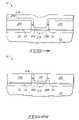
- FIG. 1illustrates a semiconductor construction 10 encompassed by particular aspects of the present invention.
- Construction 10comprises a substrate 12 .
- substrate 12the terms “semiconductive substrate” and “semiconductor substrate” are defined to mean any construction comprising semiconductive material, including, but not limited to, bulk semiconductive materials such as a semiconductive wafer (either alone or in assemblies comprising other materials thereon), and semiconductive material layers (either alone or in assemblies comprising other materials).
- substraterefers to any supporting structure, including, but not limited to, the semiconductive substrates described above.
- construction 10can correspond to a DRAM array.
- Construction 10comprises a pair of field effect transistor devices 14 and 16 supported by substrate 12 , and also comprises a device 38 having a different threshold voltage than devices 14 and 16 .
- Device 38can be utilized for electrically isolating devices 14 and 16 from one another as discussed below.
- Each of devices 14 and 16comprises a transistor gate stack 22 which includes an insulative material 24 , a conductively doped semiconductive material 26 (also referred to as a gate layer), an electrically conductive mass 28 , and an insulative cap 30 .
- Insulative material 24can comprise, for example, one or more of silicon nitride, silicon dioxide and silicon oxynitride. Insulative material 24 typically comprises silicon dioxide, and can be referred to as gate oxide.
- Conductively-doped material 26can comprise, for example, conductively-doped silicon.
- the siliconis typically in an amorphous and/or polycrystalline form.
- the dopantcan comprise n-type dopant (such as, for example, phosphorous or arsenic), or can comprise p-type dopant (such as, for example, boron).
- Conductive mass 28will typically comprise a layer of silicide formed directly on an upper surface of a silicon material 26 ; or a layer of metal formed directly on (i.e. physically against) a barrier layer of WN x or TiN, which in turn is on the silicon material 26 .
- Insulative cap 30can comprise, for example, one or both of silicon nitride and silicon dioxide.
- the gate stackscomprise sidewalls, and electrically insulative spacers 32 are formed along such sidewalls.
- Spacers 32can comprise, for example, silicon nitride, and can be formed by depositing a material conformally over substrate 12 and gate stacks 22 , and subsequently anisotropically etching such material.
- a plurality of source/drain regions 34are provided within substrate 12 and between gate stacks 22 .
- Gate stacks 22can be considered as being directly over segments of substrate 12 , and source/drain regions 34 can be considered as being spaced from one another by at least portions of such segments. In the shown constructions, source/drain regions 34 extend the entire spacer width under spacers 32 .
- Source/drain regions 34are conductively-doped diffusion regions extending into substrate 12 .
- transistor constructions 14 and 16will be NMOS transistors, and accordingly source/drain regions 34 will be n-type doped diffusion regions.
- the majority dopant within diffusion regions 34will be n-type dopant.
- the term “majority dopant”refers to the dopant that is most abundant within the regions. Accordingly, if both p-type and n-type dopant are present in the regions, the majority dopant type will be that which is most prevalent.
- the stack 36discussed in more detail below
- the stack 36discussed in more detail below
- the source/drain regions 34extend under spacers 32 in the shown construction. It is to be understood however that other structures can be formed in which the source/drain regions do not extend underneath the spacers, or even in which at least some of the spacers are eliminated. Additionally, source/drain regions 34 can extend beneath spacers 32 less than the full spacer width, can extend the full spacer width or can extend beyond the spacer to beneath the corresponding stack (not shown).
- the various source/drain regionsare connected to either capacitor constructions 42 or digit lines 44 to define various memory cell units of the DRAM memory array.
- Isolation region 38extends between transistor constructions 14 and 16 , and can be utilized to electrically isolate such transistor constructions from one another.
- Isolation region 38comprises stack 36 similar to stacks 22 of gate constructions 14 and 16 .
- Stack 36comprises the insulative material 24 , conductive mass 28 and insulative cap 34 utilized in gate stacks 22 .
- stack 36can differ from gate stacks 22 in having a heavily doped material 40 which is differentially doped than the material 26 of stacks 22 .
- material 40can comprise silicon doped with significant concentrations of an opposite type dopant as that primarily utilized in source drain regions 34 .
- material 40can primarily comprise p-type dopant.
- the utilization of p-type dopant as a majority dopant within doped gate layer 40while having source/drain regions 34 with n-type dopant as majority dopant, can cause stack 40 to have a high threshold voltage relative to adjacent devices. This can enable stack 36 to function primarily as an isolation region at particular threshold voltages utilized to drive adjacent devices, rather than as a transistor construction.
- material 40can comprise significant concentrations of both p-type and n-type dopant, and can, for example, comprise concentrations from 1 ⁇ 10 18 atoms/cm 3 to 5 ⁇ 10 21 atoms/cm 3 of both p-type and n-type dopants.
- a concentration of the dopantcan be about 1 ⁇ 10 20 atoms/cm 3 .
- material 40can comprises essentially one type of dopant (i.e. at least 99% of the dopant within material 54 can be p-type) or material 40 can effectively comprise two types of dopant (in other words, less than 99% of the dopant within material 40 is p-type).
- material 40can be majority n-doped and coupled to a suitable electrical bias so that isolation device 38 appropriately functions as a grounded gate.
- stack 36is utilized as an isolation region, it can be described as an isolation region having a mass 40 of material extending between a pair of adjacent source/drain regions 34 .
- the adjacent source/drain regionscan, as shown, extend the full spacer-width under spacers 32 associated with stack 36 .
- the adjacent source/drain regions 32can extend a partial spacer-width beneath spacers 32 or can extend under the gate electrode (i.e. can extend under mass 40 ).
- Stack 36is shown having conductive layer 28 in contact with other electrical circuitry 48 .
- the other circuitry 48can be an electrical ground associated with construction 10 , or can be slightly positive or negative relative to ground as long as device 36 does not turn on an underlying channel.
- the apparent or effective thickness of gate oxide 24 within stack 36can change relative to that of stacks 22 .
- the effective electrical thickness of the gate oxidewill be increased in stack 36 relative to stacks 22 .
- silicon layer 40has a lower effective concentration of n-type dopant than do silicon layers 26 .
- silicon layer 40has a lower effective concentration of n-type dopant than do silicon layers 26 .
- Suchcan be accomplished by initially providing layer 40 to have the same n-type dopant concentration as do layers 26 , and subsequently adding sufficient p-type dopant to layer 40 to alter electrically properties of layer 40 .
- the p-type dopant concentrationcan be sufficient to overwhelm the n-type dopant concentration (i.e. to form the p-type dopant as the majority dopant in layer 40 ), or alternatively can be sufficient to simply have a measurable effect on the work function of a transistor construction comprising stack 36 .
- a doped pocket region 46can be provided within a semiconductive material of substrate 12 beneath isolation structure 38 .
- Doped pocket region 46can be doped with a heavy p-type atom such as, for instance, indium.
- doped region 46can additionally be doped with at least one other p-type dopant such as, for example, boron. It can be advantageous to provide indium or other heavy p-type dopant, such as Ga or TI, in the pocket region 46 beneath isolation structure 38 to increase the threshold voltage of isolation gate 36 . Further, indium within pocket region 46 can enhance retention of dopant centrally beneath isolation device 38 . The relatively low diffusivity of indium can minimize diffusion of dopant toward the storage node junction and thereby minimize junction leakage.
- a lower dosage of the additional p-type dopantcan be utilized relative to concentrations typically used to minimize charge leakage between nodes across a grounded gate device 38 .
- Indiumcan be provided within pocket region 46 to a concentration of from about 1 ⁇ 10 12 atoms/cm 3 to about 1 ⁇ 10 13 atoms/cm 3 . If pocket region 46 is additionally doped with boron, boron can be provided to a concentration of from about 1 ⁇ 10 12 atoms/cm 3 to about 2 ⁇ 10 12 atoms/cm 3 .
- Activation of implanted indiumcan comprise activation by thermal processing at a temperature of about 900° C. for between about 1 minute and about 6 minutes, preferably from about 1 minute to about 2 minutes. Such activation can occur during a reflow of borophosphosilicate glass (BPSG) or can occur in an independent step.
- BPSGborophosphosilicate glass
- Doped region 46preferably has a lateral width that is less than the width of gate stack 36 .
- pocket region 46is substantially centered beneath device 38 and comprises a lateral width that is less than or equal to the total width of device 38 , the total width of device 38 being the furthest distance between outer edges of the pair of sidewall spacers 32 associated with gate stack 36 .
- the heavy p-type atom dopant in doped region 46is separated from each neighboring source/drain region 34 by a gap.
- the doped pocket regioncan be referred to as a sub-region of a doped region.
- FIG. 1shows heavily doped material 40 of gate stack 36 utilized in conjunction with doped channel region 46
- the inventionencompasses embodiments wherein material 40 is substituted with alternative conductively doped semiconductor material such as the material utilized for layer 26 in gate stacks 22 .
- construction 10can comprise doped channel regions within regions of substrate 12 underlying stacks 22 (not shown).
- doped channel regions beneath the transistor devicescan be doped with a non-heavy p-type dopant such as, for example boron.
- boron doped channel regionscan lack additionally added heavy p-type dopants and can have boron implanted to a concentration of from about 5 ⁇ 10 12 atoms/cm 3 to about 9 ⁇ 10 12 atoms/cm 3 .
- conductive mass 28can comprise a silicide layer which is formed directly on (physically against) layer 40 , and can further comprise a metal layer, metal compound layer, and/or metal alloy layer which is formed over and physically against the silicide layer.
- Stack 36can be considered to be within a DRAM array, and the array can be, for example, a 6 F 2 or 8 F 2 array.
- FIG. 1A method of forming the construction of FIG. 1 is described with references to FIGS. 2–13 . In describing FIGS. 2–13 , similar numbering will be used as was utilized above in describing FIG. 1 , as appropriate.
- wafer construction 10is shown at a preliminary processing stage.
- Construction 10comprises substrate 12 , insulative layer 24 , and a masking material 102 formed over insulative layer 24 .
- Masking material 102can comprise, for example, either positive or negative photoresist, and in particular embodiments can comprise M108YTM from JSRTM Corporation of Japan.
- photoresist 102is photolithographically patterned into a pair of adjacent and spaced blocks 104 and 106 .
- Block 104has a sidewall edge 105 and a top edge 107 . It is to be understood that the term “block” is utilized herein to generically refer to any patterned shape, including for example, rectangular shapes, square shapes or shapes with curved edges.
- blocks 104 and 106are formed in physical contact with insulative material 24 . It is to be understood that the invention encompasses other embodiments (not shown) wherein masking material 102 is formed directly on a semiconductive material of substrate 12 in the absence of insulative layer 24 to result in blocks that are physically against substrate 12 .
- a gap 110extends between patterned blocks 104 and 106 , and in the shown embodiment an upper surface 112 of insulative material 24 is exposed within gap 110 .
- Patterned blocks 104 and 106can be considered to cover a first portion of insulative layer 24 , and to leave a second portion of layer 24 uncovered. In embodiments having material 102 formed in an absence of layer 24 (not shown), patterned blocks 104 and 106 can cover a first portion of substrate 12 and leave a second portion of the substrate material uncovered.
- a coating 114is formed over patterned photoresist blocks 104 and 106 , and within gap 110 .
- Coating 114covers at least some of the portion of insulative material 24 that is exposed between blocks 104 and 106 , and in the shown embodiment covers all of the exposed portion of insulative material 24 .
- Coating 114is a material other than photoresist, and in particular applications, corresponds to a material designated as AZ R200TM by Clariant International, Ltd.
- Coating 114is physically against photoresist blocks 104 and 106 , and corresponds to a material which can be selectively removed from over exposed portion 112 of insulative material 24 , while remaining adhered to the photoresist of blocks 104 and 106 .
- coating 114corresponds to the material designated as AZ R200TM, and is coated across an entirety of a semiconductive wafer, and is subsequently spun dry.
- AZ R200TMis a water-based material, so it is preferable to conduct the procedures associated with AZ R200TM in a separate chamber from the procedures utilized in exposing and developing photoresist, since water can interfere with standard photoresist processing.
- a preferred process of the present inventioncomprises forming a photoresist mass 102 and photolithographically processing such mass in a separate “bowl” or chamber from that utilized during formation of coating 114 .
- semiconductor construction 10is baked at a temperature of from about 100° C. to about 120° C. Such baking is thought to diffuse acid from resist 102 into the AZ R200TM, and crosslink the layer of AZ R200TM across resist blocks 104 and 106 .
- the crosslinkingcan bond the coating to blocks 104 and 106 and/or form the coating into a shell tightly adhered with blocks 104 and 106 .
- the material designated as AZ R200TMis but one material which can be utilized in methodology of the present invention. Other materials which selectively bond or adhere to photoresist blocks 104 and 106 can be used alternatively to the material designated as AZ R200TM.
- coating 114is exposed to conditions which selectively remove the coating from between blocks 104 and 106 , while leaving a layer of the coating against blocks 104 and 106 .
- the coatingcomprises AZ R200TM
- such removalcan be accomplished by exposing semiconductor construction 10 to an aqueous solution comprising surfactant.
- a suitable aqueous surfactant solutionis the material marketed as “SOLUTION CTM” by Clariant International, Ltd.
- construction 10can be subjected to a so-called hard bake at a temperature of from about 130° C. to about 140° C. after removal of the non-crosslinked material. Such hard bake can fully dry and further crosslink the portions of coating 114 remaining around blocks 104 and 106 .
- the coating 114 remaining around a photoresist blockcan be considered to define a second block which extends laterally outward beyond edges of the photoresist block.
- the coating 114 over photoresist block 104defines lateral edge 116 which extends laterally outward beyond lateral edge 105 of block 104 , and also defines a top edge 115 which extends elevationally above the top edge 107 of block 104 .
- the coating 114 around block 106comprises a lateral edge 119 which extends laterally outward beyond the lateral edge 109 of block 106 , and further comprises a top edge 117 which is elevationally above the top edge 111 of block 106 .
- Photoresist block 104 and the coating 114 surrounding such photoresist block togetherdefine a masking block which is enlarged and laterally wider than was photoresist block 104 .
- photoresist block 106 and the coating 114 surrounding such photoresist block togetherdefine a masking block 120 which is enlarged and laterally wider than photoresist block 106 .
- Masking blocks 118 and 120(also referred to as enlarged blocks) have a narrower gap between them than did photoresist blocks 104 and 106 . In other words coating 114 narrows gap 110 to reduce a dimension of such gap.
- a dopant 122is implanted relative to construction 10 .
- Masking blocks 118 and 120prevent the dopant from being implanted into the blocked regions of construction 10 .
- the unblocked regioncorresponds to a region within a surface area where stack 36 ( FIG. 1 ) is ultimately to be formed.
- Implanting dopant 122forms a doped pocket region 46 as shown in FIG. 7 .
- Doped pocket region 46has a width corresponding to the narrowed width of gap 110 .
- dopant 122can comprise a single heavy p-type dopant such as indium or can comprise both a heavy p-type dopant and an additional p-type dopant such as, for example, boron.
- a non-heavy p-type dopantsuch as boron for example can be implanted into exposed region 112 ( FIG. 3 ) prior to forming coating layer 114 over photoresist blocks 104 and 106 .
- a second dopantcan be implanted after formation of enlarged blocks 118 and 120 but in an independent step either prior to or subsequent to doping with the heavy p-type dopant.
- Dopant 122can be activated by thermal processing at a temperature of from about 900° C. for about 1 minute to about 6 minutes, preferably from about 1 minute to about 2 minutes. Activation of dopant 122 can occur during reflow of BPSG or in an independent step.
- materials 102 and 114are removed from over substrate 12 .
- the present inventioncan advantageously form doped pocket regions that are narrower than can be accomplished utilizing photolithographic processing alone. Specifically, if photoresist blocks 104 and 106 ( FIG. 3 ) are considered to be as close to one another as is possible by a particular photolithographic patterning process, then processing of the present invention has effectively defined new masking blocks 118 and 120 ( FIG. 5 ) which are closer together than could be achieved by photolithographic processing alone. In other words, if gap 110 was initially formed to have a minimum feature size achievable by photolithographic processing, then the formation of coating 114 has effectively reduced the feature size of gap 110 to below the minimum achievable feature size. In particular embodiments, the reduced width of gap 110 between blocks 118 and 120 can be less than or equal to about half the width of gap 110 between blocks 104 and 106 prior to the formation of coating 114 .
- such insulative layercan be formed after the removal of materials 102 and 114 prior to subsequent processing.
- such channel regionscan be formed by implanting dopant into the appropriate areas of the substrate after removal of materials 102 and 114 .
- such channelscan be formed prior to formation of layer 102 . Formation of such channel regions can comprise implanting boron to a concentration of from about 5 ⁇ 10 12 atoms/cm 3 to about 9 ⁇ 10 12 atoms/cm 3 .
- mass 124is formed over insulative layer 24 .
- Mass 124can be undoped as initially deposited, or alternatively can be in situ doped. In the shown application, mass 124 is undoped, and accordingly has not acquired the properties of either mass 26 ( FIG. 1 ), or mass 40 ( FIG. 1 ).
- a patterned masking material 126is formed over mass 124 , and such blocks portions of mass 124 .
- Masking material 126can comprise, for example, photoresist and can be formed into the shown pattern by, for example, photolithographic processing.
- Masking material 126covers a portion of construction 10 where stack 36 is ultimately to be formed while leaving other portions of construction 10 uncovered.
- a dopant 127is implanted into construction 10 , and specifically is implanted into portions of material 124 ( FIG. 9 ) which are not covered by mask 126 . Such converts the material 124 to material 26 .
- Dopant 127can comprise,for example, n-type dopant (such as phosphorous or arsenic).
- Dopant 127can be provided to a concentration of at least 1 ⁇ 10 20 atoms/cm 3 , and typically is provided to a concentration of from about 1 ⁇ 10 20 atoms/cm 3 to about 5 ⁇ 10 21 atoms/cm 3 .
- masking material 126is removed and replaced by another patterned masking material 128 .
- Masking material 128can comprise, for example, photoresist and can be formed into the shown pattern by, for example, photolithographic processing. Masking material 128 covers some Portion of construction 110 while leaving a portion where stack 36 is ultimately to be formed uncovered.
- a dopant 129is implanted into construction 10 , and specifically is implanted into portions of material 124 ( FIG. 9 ) which are not covered by mask 128 . Such converts the material to material 40 .
- Dopant 129can comprise an opposite conductivity type relative to dopant 127 . Further, dopant 129 can be implanted to a concentration greater than 1 ⁇ 10 20 atoms/cm 3 .
- mask 126FIG. 9
- dopant 127implanted into an entirety of material 124 ( FIG. 9 ).
- mask 128can be formed and dopant 129 implanted at a concentration higher than that of dopant 127 .
- the dopant 129can then effectively overwhelm the dopant 127 within exposed (unblocked) region of construction 10 to form doped materials 40 and 26 .
- layer 28can comprise silicide, metal, metal compounds and/or metal alloys; and layer 30 can comprise an insulative material such as, for example, silicon dioxide and/or silicon nitride.
- stacks 22 and 36are patterned from the layers 24 , 26 , 28 , 30 and 40 of FIG. 12 .
- Such patterningcan be accomplished by, for example, forming a patterned photoresist mask (not shown) over the layers, and subsequently transferring a pattern from the mask through the layers utilizing suitable etching conditions.
- the stacks 22 and 36can be incorporated into the constructions of FIG. 1 by forming source/drain regions 34 (shown in FIG. 1 ) within substrate 12 , and forming sidewall spacers 32 (shown in FIG. 1 ).
- Source/drain regions 34preferably can be formed to extend beneath sidewall spacers 32 of the of the corresponding transistor device 14 and 16 or isolation device 38 , without extending beneath the corresponding stack 22 or 36 .
- FIGS. 14–20Another application of the invention is described with reference to FIGS. 14–20 . Similar numbering will be utilized in describing FIGS. 14–20 as was used above in describing FIGS. 1–13 where appropriate.
- Construction 10 shown in FIG. 14can comprise all of the features shown in FIG. 1 , and can additionally comprise one or both of channel pocket implants 45 and 47 within channel regions underlying transistor gate stacks 22 .
- Channel pocket regions 45 and 47can comprise implants of heavy p-type atoms such as, for example, indium.
- doped pocket regions 45 and 47 and the corresponding surrounding channel areacan be additionally doped with a second p-type dopant such as, for example, boron. It can be advantageous to utilize indium pocket implants within a boron doped channel region of transistor devices to decrease the concentration of boron utilized in the channel region.
- the boron dose utilized in the channel regioncan be from about 1 ⁇ 10 12 atoms/cm 3 to about 2 ⁇ 10 12 atoms/cm 3 relative to typical boron dosed of from about 5 ⁇ 10 12 atoms/cm 3 to about 1 ⁇ 10 13 atoms/cm 3 that are utilized in channel regions in the absence of the channel pockets 45 and 47 of the present invention.
- FIG. 14A method for forming the construction of FIG. 14 is described with reference to FIGS. 15–20 .
- the methods utilized in forming the construction shown in FIG. 14can be as described above in reference to formation of the FIG. 1 construction, combined with the following alternative processing steps.
- wafer construction 10is shown at an alternative processing stage subsequent to FIG. 2 .
- Masking material 102FIG. 2
- Gaps 210extend between patterned blocks 203 and 204 , between patterned blocks 204 and 206 , and between pattern d blocks 206 and 208 .
- an upper surface 212 of insulative layer 24is exposed within gaps 210 .
- patterned blocks 203 , 204 , 206 and 208can be formed in the absence of layer 24 (not shown) and upper surface 212 can comprise a semiconductive material of substrate 12 .
- coating 114is formed over patterned photoresist blocks 203 , 204 , 206 and 208 , and within gaps 210 .
- coating 114can be selectively removed from between the patterned photoresist blocks thereby forming the narrowed gaps 210 as shown in FIG. 17 .
- narrowed gaps 210can comprise a width that is less than or equal to about half the width of the gaps prior to formation of coating 114 .
- selective removal of coating 114can form enlarged blocks 218 , 219 , 220 and 221 .
- a dopant 122is implanted into construction 10 , and specifically is implanted into portions of substrate 12 which are not covered by mask blocks 218 , 219 , 220 and 221 .
- dopant 122( FIG. 18 ) is implanted to form channel pocket regions 45 and 47 , and pocket region 46 .
- Such pocket regionshave a width corresponding to the width of narrowed gap 210 .
- dopant 122can comprise indium and in particular embodiments can additionally comprise an additional p-type dopant such as, for example, boron.
- pocket regions 45 , 46 and 47can be implanted with indium in the absence of additional dopants or can simultaneously be implanted with both indium and, for example, boron.
- Doped pocket region 46corresponds to a region of the substrate which will eventually underlie isolation device 38 ( FIG. 14 ).
- Doped channel pocket region 45is substantially centrally located within a channel region that will eventually be associated with transistor device 14 ( FIG. 14 ).
- channel pocket region 47corresponds to a substantially center d subregion within a channel region that will eventually underlie transistor device 16 ( FIG. 14 ).
- boron and/or other dopantscan be implanted into at least one of the channel regions that will underlie devices 14 and 16 , or the corresponding region beneath isolation device 38 , in an independent doping step that is independent from implanting dopant 122 .
- Such independent stepcan occur prior to formation of resist blocks 203 , 204 , 206 and 208 ( FIG. 15 ) or can occur after formation of the patterned resist blocks but prior to formation of enlarged blocks 218 , 219 , 220 and 221 ( FIG. 17 ).
- the independent dopingcan occur after formation of enlarged masking blocks 218 , 219 , 220 and 221 in an independent step prior to or subsequent to indium implant 122 .
- Activation of indiumcan comprise heat processing as described above.
- indium diffusion from the pocket region into the surrounding substrateis minimized.
- indium doped pockets 45 and 47can be sub-regions of larger channel regions formed by boron diffusion.
- the doped pockets 45 , 46 , and 47remain narrower than width of the overlying stack. In particular embodiments, the width of the pockets will remain about the width of narrowed gap.
- semiconductor construction 10as shown in FIG. 20 , can then be processed as discussed above ( FIGS. 10–13 and corresponding text) to form the constructions shown in FIG. 14 .
- High concentrations of p-type dopants at or surrounding a storage node junctioncan increase charge leakage. Accordingly, decreasing an amount of high diffusivity dopant such as, for example, boron, utilized in the channel region can assist in decreasing leakage.
- FIG. 21shows an alternative semiconductor construction 10 that can be formed utilizing methods of the present invention.
- the construction shown in FIG. 21can be identical to the construction shown in FIG. 14 with an exception being the absence of the pocket implant region underlying isolation device 38 .
- FIG. 21depicts a complete absence of pocket implant beneath the isolation device, the invention encompasses constructions having a pocket lightly doped with indium (i.e. less than about 1 ⁇ 10 12 atoms/cm 3 , not shown).
- the isolation devicecan comprise a majority p-type doped layer 40 (discussed above).
- FIG. 21can be formed utilizing the methods discussed with reference to FIGS. 15–20 above combined with alternative photolithographic patterning of the masking material 102 ( FIG. 2 ). Such alternate patterning can expose regions of the substrate corresponding to the eventual location of transistor devices 14 and 16 while covering other areas of the substrate, including the area that will eventually underlie isolation device 38 .
- FIG. 22illustrates a semiconductor construction 10 encompassed by another aspect of the present invention.
- Construction 10can be formed by optional processing steps in addition to those described with reference to forming the construction shown in FIG. 14 .
- at least some of the source/drain regions 34 present in construction 10can comprise extension regions 50 , 52 which can extend the associated source/drain region farther beneath an associated gate device 14 , 16 .
- Extension regions 50 and 52can extend the associated source/drain region 34 such that the source drain region extends the full width of an overlying spacer 32 .
- the extensionscan extend the source/drain region to less than the full spacer width beneath the corresponding device, or can extend the source/drain region partially beneath gate stack 22 .
- source/drain regions 34can be majority doped with n-type dopant, and extension regions 50 and 52 can be majority doped with a p-type dopant.
- extensions 50 and 52can comprise a heavy p-type dopant such as, for example, indium.
- An appropriate indium concentration within the extensionscan be from about 1 ⁇ 10 12 atoms/cm 2 to about 3 ⁇ 10 12 atoms/cm 2 .
- semiconductor construction 10comprising source/drain extensions 50 , 52 can be formed to have such extensions beneath only one of the pair of sidewalls 32 associated with a given stack 22 .
- extension implants 50 , 52can be provided on a single side of a corresponding transistor device 14 , 16 .
- extensions 50 and 52are provided only on bit contact sides of gates 14 and 26 and are absent from the source/drain region on the opposing storage node sides of the gates. It can be advantageous to utilize indium implant extensions of source/drain regions associated with bit contact sides of transistor devices 14 and 16 to allow a reduction in the amount of indium utilized in channel pocket implants 45 and 47 .
- pocket channel regions 45 and 47can comprise an indium concentration of from about 2 ⁇ 10 12 atoms/cm 2 to about 5 ⁇ 10 12 atoms/cm 2 and can additionally comprise boron at the concentrations set forth above with respect to the semiconductor construction shown in FIG. 14 .
- FIG. 23such illustrates further processing of a construction similar to that shown in FIG. 14 prior to connection to any capacitor construction or digit lines.
- a masking material 174is formed over construction 10 and is patterned to expose portions of the substrate on what will be future bit line contact sides of transistor devices 14 and 16 .
- Masking material 174can comprise, for example, photoresist; and can be patterned utilizing suitable photolithographic processes.
- a dopant 176is implanted relative to construction 10 and forms extension regions 50 and 52 shown in FIG. 24 .
- Dopant 176can be implanted using angled implant techniques typically utilized for forming halo implants relative to a gate. Implant regions 50 and 52 differ from typical halo implants, however, in that implants 50 and 52 do not form a ring shaped structure since dopant is implanted only on one side of the corresponding gate, the opposing side of the gate being blocked by masking material 174 .
- Dopant 176can comprise a p-type dopant and preferably comprises a heavy p-type dopant such as indium.
- the semiconductor construction shown in FIG. 24can be further processed to remove photoresist material 174 and to form the construction shown in FIG. 22 .
- FIG. 25illustrates a semiconductor construction 10 encompassed by another aspect of the present invention and will be described using similar numbering as was used above in FIGS. 1–24 where appropriate.
- the construction 10 shown in FIG. 25is similar to the construction illustrated in FIG. 22 with an exception being the presence of a shallow trench isolation region 54 in place of the isolation device 38 ( FIG. 14 ).
- construction 10 as shown in FIG. 25can be formed utilizing conventional shallow trench isolation region formation combined with various methods of the present invention described above.
- Shallow trench region 54can be formed at an initial processing step prior to formation of patternable material 102 ( FIG. 2 ). Material 102 can then be patterned by methods discussed above to expose the regions of substrate while leaving other regions covered.
- Coating material 144can be formed and processed to expose regions that will eventually underlie central portions of stacks 22 while other regions, including the shallow trench isolation region, remain masked.
- Channel pockets 45 and 47can then be formed as described above, followed by formation of the additional features shown in FIG. 25 .
- FIGS. 22 and 25show implant extensions 50 and 52 being utilized in conjunction with channel pocket regions 45 and 47 , it is to be understood that the invention encompasses embodiments wherein extensions 50 and 52 are utilized in semiconductor constructions in an absence of the described pocket regions 45 and 47 .
- the inventionincludes damascene processes for forming gate constructions.
- An exemplary method of forming a construction utilizing a damascene processis described with reference to FIGS. 26–29 .
- an initial stepcan comprise depositing a layer of dielectric material 202 over insulative material 24 .
- dielectric layer 202can be deposited on substrate 12 in an absence of an insulative layer and insulative material 24 can be grown after the damascene process.
- Source-drain regions 34can be present prior to depositing dielectric layer 202 as shown in FIG. 26 , or can be formed during or after gate formation.
- Dielectric material 202can be patterned by conventional methods, such as photolithography, to form patterned blocks 203 and 205 , the blocks having sidewalls 204 and 206 being separated by a gap.
- Removable spacers 208can be formed along sidewalls 204 and 206 .
- Removable spacers 208can be formed for example, by depositing a layer of sacrificial material and anisotropically etching the sacrificial material. Spacers 208 have lateral edges 209 and 211 that are separated by a narrowed gap relative to the distance between sidewalls 204 and 206 .
- a dopant 122(discussed above) is implanted relative to construction 10 to form a doped pocket region 212 as shown in FIG. 27 .
- Doped pocket region 212has a width corresponding to the width between lateral edges 209 and 211 .
- spacers 208are removed and a layer of polysilicon 214 is conformally deposited over construction 10 and along sidewalls 204 and 206 .
- a gate electrode material 216such as WN/W or other compositions comprising a metal and/or metal nitride, can be deposited over polysilicon layer as shown in FIG. 28 .
- a planarization step utilizing for example chemical mechanical polishingis performed to form the planarized gate structure having a metal gate electrode 220 as shown.
- the gate structurecan have a gate structure width corresponding to the distance between the sidewalls 204 and 206 .
- doped pocket region 212can have a width that is less than the width of the gate structure and in particular embodiments, pocket region 112 can comprise a width less than or equal to about half the width of the gate structure.
- a channel region which underlies the damascene gate structure and surrounding pocket (shown in FIG. 29 ) regioncan additionally comprise boron as discussed above relative to gate stack structures 22 and 36 .
- Source-drain extensions(not shown) can b utilized in conjunction with the gate and can be formed as described above.
Landscapes
- Engineering & Computer Science (AREA)
- Manufacturing & Machinery (AREA)
- Physics & Mathematics (AREA)
- Condensed Matter Physics & Semiconductors (AREA)
- General Physics & Mathematics (AREA)
- Computer Hardware Design (AREA)
- Microelectronics & Electronic Packaging (AREA)
- Power Engineering (AREA)
- Insulated Gate Type Field-Effect Transistor (AREA)
- Metal-Oxide And Bipolar Metal-Oxide Semiconductor Integrated Circuits (AREA)
- Semiconductor Memories (AREA)
Abstract
Description
Claims (5)
Priority Applications (1)
| Application Number | Priority Date | Filing Date | Title |
|---|---|---|---|
| US10/624,627US7087478B2 (en) | 2002-08-26 | 2003-07-21 | Methods of forming semiconductor constructions |
Applications Claiming Priority (3)
| Application Number | Priority Date | Filing Date | Title |
|---|---|---|---|
| US10/229,336US6756619B2 (en) | 2002-08-26 | 2002-08-26 | Semiconductor constructions |
| US10/364,054US7045449B2 (en) | 2002-08-26 | 2003-02-10 | Methods of forming semiconductor constructions |
| US10/624,627US7087478B2 (en) | 2002-08-26 | 2003-07-21 | Methods of forming semiconductor constructions |
Related Parent Applications (1)
| Application Number | Title | Priority Date | Filing Date |
|---|---|---|---|
| US10/364,054DivisionUS7045449B2 (en) | 2002-08-26 | 2003-02-10 | Methods of forming semiconductor constructions |
Publications (2)
| Publication Number | Publication Date |
|---|---|
| US20040094788A1 US20040094788A1 (en) | 2004-05-20 |
| US7087478B2true US7087478B2 (en) | 2006-08-08 |
Family
ID=31887653
Family Applications (11)
| Application Number | Title | Priority Date | Filing Date |
|---|---|---|---|
| US10/229,336Expired - LifetimeUS6756619B2 (en) | 2002-08-26 | 2002-08-26 | Semiconductor constructions |
| US10/364,054Expired - Fee RelatedUS7045449B2 (en) | 2002-08-26 | 2003-02-10 | Methods of forming semiconductor constructions |
| US10/367,520Expired - LifetimeUS7157775B2 (en) | 2002-08-26 | 2003-02-13 | Semiconductor constructions |
| US10/624,628Expired - LifetimeUS7091113B2 (en) | 2002-08-26 | 2003-07-21 | Methods of forming semiconductor constructions |
| US10/624,716Expired - LifetimeUS7285468B2 (en) | 2002-08-26 | 2003-07-21 | Methods of forming semiconductor constructions |
| US10/624,627Expired - LifetimeUS7087478B2 (en) | 2002-08-26 | 2003-07-21 | Methods of forming semiconductor constructions |
| US11/211,911AbandonedUS20060022279A1 (en) | 2002-08-26 | 2005-08-24 | Semiconductor constructions |
| US11/211,374Expired - LifetimeUS7227227B2 (en) | 2002-08-26 | 2005-08-24 | Reduced leakage semiconductor device |
| US11/211,413AbandonedUS20050280033A1 (en) | 2002-08-26 | 2005-08-24 | Semiconductor constructions |
| US11/211,373Expired - LifetimeUS7274056B2 (en) | 2002-08-26 | 2005-08-24 | Semiconductor constructions |
| US11/338,175AbandonedUS20060121712A1 (en) | 2002-08-26 | 2006-01-23 | Semiconductor constructions and methods of forming semiconductor constructions |
Family Applications Before (5)
| Application Number | Title | Priority Date | Filing Date |
|---|---|---|---|
| US10/229,336Expired - LifetimeUS6756619B2 (en) | 2002-08-26 | 2002-08-26 | Semiconductor constructions |
| US10/364,054Expired - Fee RelatedUS7045449B2 (en) | 2002-08-26 | 2003-02-10 | Methods of forming semiconductor constructions |
| US10/367,520Expired - LifetimeUS7157775B2 (en) | 2002-08-26 | 2003-02-13 | Semiconductor constructions |
| US10/624,628Expired - LifetimeUS7091113B2 (en) | 2002-08-26 | 2003-07-21 | Methods of forming semiconductor constructions |
| US10/624,716Expired - LifetimeUS7285468B2 (en) | 2002-08-26 | 2003-07-21 | Methods of forming semiconductor constructions |
Family Applications After (5)
| Application Number | Title | Priority Date | Filing Date |
|---|---|---|---|
| US11/211,911AbandonedUS20060022279A1 (en) | 2002-08-26 | 2005-08-24 | Semiconductor constructions |
| US11/211,374Expired - LifetimeUS7227227B2 (en) | 2002-08-26 | 2005-08-24 | Reduced leakage semiconductor device |
| US11/211,413AbandonedUS20050280033A1 (en) | 2002-08-26 | 2005-08-24 | Semiconductor constructions |
| US11/211,373Expired - LifetimeUS7274056B2 (en) | 2002-08-26 | 2005-08-24 | Semiconductor constructions |
| US11/338,175AbandonedUS20060121712A1 (en) | 2002-08-26 | 2006-01-23 | Semiconductor constructions and methods of forming semiconductor constructions |
Country Status (9)
| Country | Link |
|---|---|
| US (11) | US6756619B2 (en) |
| EP (1) | EP1532678A2 (en) |
| JP (1) | JP2005536893A (en) |
| KR (1) | KR100642404B1 (en) |
| CN (2) | CN1941380B (en) |
| AU (1) | AU2003270029A1 (en) |
| SG (1) | SG149698A1 (en) |
| TW (1) | TWI232548B (en) |
| WO (1) | WO2004019384A2 (en) |
Families Citing this family (34)
| Publication number | Priority date | Publication date | Assignee | Title |
|---|---|---|---|---|
| KR100937650B1 (en)* | 2002-12-30 | 2010-01-19 | 동부일렉트로닉스 주식회사 | Transistor manufacturing method of semiconductor device |
| US6936518B2 (en)* | 2004-01-21 | 2005-08-30 | Intel Corporation | Creating shallow junction transistors |
| US8996722B2 (en)* | 2004-11-01 | 2015-03-31 | Alcatel Lucent | Softrouter feature server |
| US20060134917A1 (en)* | 2004-12-16 | 2006-06-22 | Lam Research Corporation | Reduction of etch mask feature critical dimensions |
| KR20060076011A (en)* | 2004-12-29 | 2006-07-04 | 삼성전자주식회사 | Semiconductor element and method of forming the same |
| US20070015847A1 (en)* | 2005-07-15 | 2007-01-18 | Applied Materials, Inc. | Red printing ink for color filter applications |
| US20070176016A1 (en)* | 2006-02-01 | 2007-08-02 | Green Kenneth I | Sprinkler station expander |
| US8852851B2 (en) | 2006-07-10 | 2014-10-07 | Micron Technology, Inc. | Pitch reduction technology using alternating spacer depositions during the formation of a semiconductor device and systems including same |
| US8106519B2 (en)* | 2008-04-22 | 2012-01-31 | Macronix International Co., Ltd. | Methods for pitch reduction |
| US7989307B2 (en) | 2008-05-05 | 2011-08-02 | Micron Technology, Inc. | Methods of forming isolated active areas, trenches, and conductive lines in semiconductor structures and semiconductor structures including the same |
| US10151981B2 (en) | 2008-05-22 | 2018-12-11 | Micron Technology, Inc. | Methods of forming structures supported by semiconductor substrates |
| US8409457B2 (en)* | 2008-08-29 | 2013-04-02 | Micron Technology, Inc. | Methods of forming a photoresist-comprising pattern on a substrate |
| US8039399B2 (en)* | 2008-10-09 | 2011-10-18 | Micron Technology, Inc. | Methods of forming patterns utilizing lithography and spacers |
| US8273634B2 (en)* | 2008-12-04 | 2012-09-25 | Micron Technology, Inc. | Methods of fabricating substrates |
| US8247302B2 (en) | 2008-12-04 | 2012-08-21 | Micron Technology, Inc. | Methods of fabricating substrates |
| US8796155B2 (en) | 2008-12-04 | 2014-08-05 | Micron Technology, Inc. | Methods of fabricating substrates |
| US8268543B2 (en)* | 2009-03-23 | 2012-09-18 | Micron Technology, Inc. | Methods of forming patterns on substrates |
| US9330934B2 (en) | 2009-05-18 | 2016-05-03 | Micron Technology, Inc. | Methods of forming patterns on substrates |
| US20110129991A1 (en)* | 2009-12-02 | 2011-06-02 | Kyle Armstrong | Methods Of Patterning Materials, And Methods Of Forming Memory Cells |
| US8518788B2 (en) | 2010-08-11 | 2013-08-27 | Micron Technology, Inc. | Methods of forming a plurality of capacitors |
| US8455341B2 (en) | 2010-09-02 | 2013-06-04 | Micron Technology, Inc. | Methods of forming features of integrated circuitry |
| JP2012256012A (en)* | 2010-09-15 | 2012-12-27 | Semiconductor Energy Lab Co Ltd | Display device |
| US8575032B2 (en) | 2011-05-05 | 2013-11-05 | Micron Technology, Inc. | Methods of forming a pattern on a substrate |
| US9076680B2 (en) | 2011-10-18 | 2015-07-07 | Micron Technology, Inc. | Integrated circuitry, methods of forming capacitors, and methods of forming integrated circuitry comprising an array of capacitors and circuitry peripheral to the array |
| US8669620B2 (en)* | 2011-12-20 | 2014-03-11 | Mika Nishisaka | Semiconductor device and method of manufacturing the same |
| US9177794B2 (en) | 2012-01-13 | 2015-11-03 | Micron Technology, Inc. | Methods of patterning substrates |
| US8629048B1 (en) | 2012-07-06 | 2014-01-14 | Micron Technology, Inc. | Methods of forming a pattern on a substrate |
| US8796098B1 (en)* | 2013-02-26 | 2014-08-05 | Cypress Semiconductor Corporation | Embedded SONOS based memory cells |
| US9337190B2 (en)* | 2013-03-12 | 2016-05-10 | Taiwan Semiconductor Manufacturing Company, Ltd. | Semiconductor device including dummy isolation gate structure and method of fabricating thereof |
| US9997617B2 (en) | 2013-03-13 | 2018-06-12 | Qualcomm Incorporated | Metal oxide semiconductor (MOS) isolation schemes with continuous active areas separated by dummy gates and related methods |
| US11430895B2 (en)* | 2020-06-03 | 2022-08-30 | Micron Technology, Inc. | Transistors including oxide semiconductive materials, and related microelectronic devices, memory devices, electronic systems, and methods |
| KR20220049742A (en)* | 2020-10-15 | 2022-04-22 | 삼성전기주식회사 | Printed circuit board |
| CN115701211B (en)* | 2021-07-16 | 2025-09-26 | 长鑫存储技术有限公司 | Semiconductor structure and manufacturing method thereof |
| CN116896270A (en)* | 2022-04-11 | 2023-10-17 | 力旺电子股份有限公司 | Voltage converter and method of operation |
Citations (90)
| Publication number | Priority date | Publication date | Assignee | Title |
|---|---|---|---|---|
| US3886003A (en) | 1971-10-04 | 1975-05-27 | Fujitsu Ltd | Method of making an integrated circuit |
| US4366338A (en) | 1981-01-09 | 1982-12-28 | Massachusetts Institute Of Technology | Compensating semiconductor materials |
| US4570331A (en) | 1984-01-26 | 1986-02-18 | Inmos Corporation | Thick oxide field-shield CMOS process |
| US4686000A (en) | 1985-04-02 | 1987-08-11 | Heath Barbara A | Self-aligned contact process |
| US4838991A (en) | 1987-10-30 | 1989-06-13 | International Business Machines Corporation | Process for defining organic sidewall structures |
| US4937756A (en) | 1988-01-15 | 1990-06-26 | Industrial Technology Research Institute | Gated isolated structure |
| US4985740A (en)* | 1989-06-01 | 1991-01-15 | General Electric Company | Power field effect devices having low gate sheet resistance and low ohmic contact resistance |
| JPH04105328A (en) | 1990-08-24 | 1992-04-07 | Mitsubishi Electric Corp | Manufacturing method of semiconductor device |
| US5164806A (en) | 1990-05-23 | 1992-11-17 | Mitsubishi Denki Kabushiki Kaisha | Element isolating structure of semiconductor device suitable for high density integration |
| US5225704A (en) | 1988-07-08 | 1993-07-06 | Mitsubishi Denki Kabushiki Kaisha | Field shield isolation structure for semiconductor memory device and method for manufacturing the same |
| US5355012A (en) | 1990-10-03 | 1994-10-11 | Mitsubishi Denki Kabushiki Kaisha | Semiconductor device |
| US5369295A (en) | 1992-01-28 | 1994-11-29 | Thunderbird Technologies, Inc. | Fermi threshold field effect transistor with reduced gate and diffusion capacitance |
| US5397909A (en) | 1990-10-12 | 1995-03-14 | Texas Instruments Incorporated | High-performance insulated-gate field-effect transistor |
| US5440161A (en) | 1993-07-27 | 1995-08-08 | Mitsubishi Denki Kabushiki Kaisha | Semiconductor device having an SOI structure and a manufacturing method thereof |
| EP0718881A2 (en) | 1994-12-20 | 1996-06-26 | STMicroelectronics, Inc. | Isolation by active transistors with grounded gates |
| US5532107A (en) | 1989-11-17 | 1996-07-02 | Nippon Zeon Co., Ltd. | Positive resist composition |
| US5534456A (en) | 1994-05-25 | 1996-07-09 | Sandisk Corporation | Method of making dense flash EEPROM cell array and peripheral supporting circuits formed in deposited field oxide with sidewall spacers |
| US5635744A (en) | 1994-09-08 | 1997-06-03 | Mitsubushi Denki Kabushiki Kaisha | Semiconductor memory and semiconductor device having SOI structure |
| US5654573A (en) | 1994-11-28 | 1997-08-05 | Mitsubishi Denki Kabushiki Kaisha | Semiconductor device having SOI structure and manufacturing method therefor |
| US5672526A (en) | 1993-12-28 | 1997-09-30 | Nippon Steel Corporation | Method of fabricating a semiconductor device using element isolation by field shield |
| US5688705A (en) | 1994-02-17 | 1997-11-18 | National Semiconductor Corporation | Method for reducing the spacing between the horizontally adjacent floating gates of a flash EPROM array |
| US5767557A (en) | 1994-12-01 | 1998-06-16 | Lucent Technologies Inc. | PMOSFETS having indium or gallium doped buried channels and n+polysilicon gates and CMOS devices fabricated therefrom |
| US5814875A (en) | 1995-01-31 | 1998-09-29 | Nippon Steel Corporation | Semiconductor device and method of manufacturing the same apparatus and method for providing semiconductor devices having a field shield element between devices |
| US5841185A (en) | 1995-02-17 | 1998-11-24 | Nippon Steel Corporation | Semiconductor device having CMOS transistors |
| US5856226A (en) | 1997-12-19 | 1999-01-05 | Texas Instruments-Acer Incorporated | Method of making ultra-short channel MOSFET with self-aligned silicided contact and extended S/D junction |
| US5858847A (en) | 1997-03-28 | 1999-01-12 | Chartered Semiconductor Manufacturing, Ltd. | Method for a lightly doped drain structure |
| US5866934A (en) | 1997-06-20 | 1999-02-02 | Advanced Micro Devices, Inc. | Parallel and series-coupled transistors having gate conductors formed on sidewall surfaces of a sacrificial structure |
| US5866448A (en) | 1997-07-30 | 1999-02-02 | Chartered Semiconductor Manufacturing Ltd. | Procedure for forming a lightly-doped-drain structure using polymer layer |
| US5877056A (en) | 1998-01-08 | 1999-03-02 | Texas Instruments-Acer Incorporated | Ultra-short channel recessed gate MOSFET with a buried contact |
| US5893728A (en) | 1994-09-01 | 1999-04-13 | Mitsubishi Denki Kabushiki Kaisha | Semiconductor device having a floating node that can maintain a predetermined potential for long time, a semiconductor memory device having high data maintenance performance, and a method of manufacturing thereof |
| US5904530A (en) | 1991-05-15 | 1999-05-18 | Goldstar Electron Co., Ltd. | Method of making LDD structure spaced from channel doped region |
| US5923975A (en) | 1996-01-22 | 1999-07-13 | Sgs-Thomson Microelectronics S.R.L. | Fabrication of natural transistors in a nonvolatile memory process |
| US5930614A (en) | 1988-09-29 | 1999-07-27 | Mitsubishi Denki Kabushiki Kaisha | Method for forming MOS device having field shield isolation |
| US5946568A (en) | 1996-05-17 | 1999-08-31 | Mosel Vitelic, Inc. | Self aligned method of fabricating a DRAM with improved capacitance |
| US5970352A (en) | 1998-04-23 | 1999-10-19 | Kabushiki Kaisha Toshiba | Field effect transistor having elevated source and drain regions and methods for manufacturing the same |
| US6001707A (en) | 1998-12-07 | 1999-12-14 | United Semiconductor Corp. | Method for forming shallow trench isolation structure |
| US6008115A (en) | 1997-04-10 | 1999-12-28 | Lg Semicon Co., Ltd. | Method for forming structure of wires for a semiconductor device |
| US6033952A (en) | 1998-11-30 | 2000-03-07 | Mitsubishi Denki Kabushiki Kaisha | Method of manufacturing a semiconductor device |
| US6060364A (en) | 1999-03-02 | 2000-05-09 | Advanced Micro Devices, Inc. | Fast Mosfet with low-doped source/drain |
| US6124168A (en) | 1991-08-14 | 2000-09-26 | Intel Corporation | Method for forming an asymmetric floating gate overlap for improved device performance in buried bit-line devices |
| US6144079A (en) | 1996-04-01 | 2000-11-07 | Mitsubishi Denki Kabushiki Kaisha | Semiconductor device and method of manufacturing the same |
| US6180468B1 (en) | 1998-10-23 | 2001-01-30 | Advanced Micro Devices Inc. | Very low thermal budget channel implant process for semiconductors |
| US6187624B1 (en) | 1999-06-04 | 2001-02-13 | Taiwan Semiconductor Manufacturing Company | Method for making closely spaced capacitors with reduced parasitic capacitance on a dynamic random access memory (DRAM) device |
| US6194276B1 (en) | 1999-09-10 | 2001-02-27 | Stmicroelectronics, Inc. | Radiation hardened semiconductor memory |
| US6204536B1 (en) | 1997-10-22 | 2001-03-20 | Mitsubishi Denki Kabushiki Kaisha | Semiconductor device and manufacturing method thereof |
| US6207510B1 (en) | 1999-01-12 | 2001-03-27 | Lucent Technologies Inc. | Method for making an integrated circuit including high and low voltage transistors |
| US6228731B1 (en) | 1999-08-16 | 2001-05-08 | Taiwan Semiconductor Manufacturing Company | Re-etched spacer process for a self-aligned structure |
| US6242329B1 (en) | 1999-02-03 | 2001-06-05 | Advanced Micro Devices, Inc. | Method for manufacturing asymmetric channel transistor |
| US6251744B1 (en) | 1999-07-19 | 2001-06-26 | Taiwan Semiconductor Manufacturing Company | Implant method to improve characteristics of high voltage isolation and high voltage breakdown |
| US20010006752A1 (en) | 1998-04-13 | 2001-07-05 | Fujitsu Limited | Resist composition and pattern forming process |
| US6277720B1 (en) | 1997-06-30 | 2001-08-21 | Texas Instruments Incorporated | Silicon nitride dopant diffusion barrier in integrated circuits |
| US6297082B1 (en) | 1999-08-25 | 2001-10-02 | United Microelectronics Corp. | Method of fabricating a MOS transistor with local channel ion implantation regions |
| US6297132B1 (en) | 2000-02-07 | 2001-10-02 | Chartered Semiconductor Manufacturing Ltd. | Process to control the lateral doping profile of an implanted channel region |
| US20010036713A1 (en) | 1997-12-05 | 2001-11-01 | Rodder Mark S. | Sidewall process and method of implantation for improved CMOS with benefit of low CGD, improved doping profiles, and insensitivity to chemical processing |
| US6331458B1 (en) | 1994-10-11 | 2001-12-18 | Advanced Micro Devices, Inc. | Active region implant methodology using indium to enhance short channel performance of a surface channel PMOS device |
| US20020006693A1 (en) | 2000-07-13 | 2002-01-17 | Nec Corporation | Semiconductor device and the manufacturing method thereof |
| US6359319B1 (en) | 1997-04-25 | 2002-03-19 | Nec Corporation | Static random access memory cell having pocket regions adjacent to sources of drive transistors |
| US20020034865A1 (en) | 1999-05-14 | 2002-03-21 | Hiroyuki Umimoto | Semiconductor device and method of fabricating the same |
| US6362034B1 (en) | 1999-12-20 | 2002-03-26 | Intel Corporation | Method of forming MOSFET gate electrodes having reduced depletion region growth sensitivity to applied electric field |
| US20020043692A1 (en) | 1998-10-26 | 2002-04-18 | Shigenobu Maeda | Semiconductor storage device |
| US6380598B1 (en) | 1994-12-20 | 2002-04-30 | Stmicroelectronics, Inc. | Radiation hardened semiconductor memory |
| US6420749B1 (en) | 2000-06-23 | 2002-07-16 | International Business Machines Corporation | Trench field shield in trench isolation |
| US6429491B1 (en) | 1999-10-20 | 2002-08-06 | Transmeta Corporation | Electrostatic discharge protection for MOSFETs |
| US6436747B1 (en) | 1999-04-21 | 2002-08-20 | Matsushita Electtric Industrial Co., Ltd. | Method of fabricating semiconductor device |
| US6444548B2 (en) | 1999-02-25 | 2002-09-03 | International Business Machines Corporation | Bitline diffusion with halo for improved array threshold voltage control |
| US6451704B1 (en) | 2001-05-07 | 2002-09-17 | Chartered Semiconductor Manufacturing Ltd. | Method for forming PLDD structure with minimized lateral dopant diffusion |
| US6458666B2 (en) | 2000-06-09 | 2002-10-01 | Texas Instruments Incorporated | Spot-implant method for MOS transistor applications |
| US6468865B1 (en) | 2000-11-28 | 2002-10-22 | Advanced Micro Devices, Inc. | Method of simultaneous formation of bitline isolation and periphery oxide |
| US20020164846A1 (en) | 1999-03-03 | 2002-11-07 | Xi-Wei Lin | Integrated circuit devices with high and low voltage components and processes for manufacturing these devices |
| US6479330B2 (en) | 1997-06-24 | 2002-11-12 | Mitsubishi Denki Kabushiki Kaisha | Semiconductor device and method for manufacturing the same |
| US20020182829A1 (en) | 2001-05-31 | 2002-12-05 | Chia-Hsing Chen | Method for forming nitride read only memory with indium pocket region |
| US6492694B2 (en) | 1998-02-27 | 2002-12-10 | Micron Technology, Inc. | Highly conductive composite polysilicon gate for CMOS integrated circuits |
| US6506647B2 (en) | 2000-10-11 | 2003-01-14 | Hitachi, Ltd. | Method for fabricating a semiconductor integrated circuit device |
| US6512269B1 (en) | 2000-09-07 | 2003-01-28 | International Business Machines Corporation | High-voltage high-speed SOI MOSFET |
| US6515899B1 (en) | 2001-11-09 | 2003-02-04 | Lattice Semiconductor Corporation | Non-volatile memory cell with enhanced cell drive current |
| US6518113B1 (en)* | 2001-02-06 | 2003-02-11 | Advanced Micro Devices, Inc. | Doping of thin amorphous silicon work function control layers of MOS gate electrodes |
| US20030030112A1 (en) | 2001-06-29 | 2003-02-13 | Fujitsu Limited | Semiconductor device having pocket and manufacture thereof |
| US6521487B1 (en) | 2001-12-05 | 2003-02-18 | United Microelectronics Corp. | Method for making a thyristor |
| US20030071310A1 (en) | 2001-10-11 | 2003-04-17 | Salling Craig T. | Method to increase substrate potential in MOS transistors used in ESD protection circuits |
| US6552401B1 (en) | 2000-11-27 | 2003-04-22 | Micron Technology | Use of gate electrode workfunction to improve DRAM refresh |
| US6570233B2 (en) | 2000-12-27 | 2003-05-27 | Mitsubishi Denki Kabushiki Kaisha | Method of fabricating an integrated circuit |
| US6586803B2 (en) | 1995-02-17 | 2003-07-01 | Mitsubishi Denki Kabushiki Kaisha | Semiconductor device using an SOI substrate |
| US6599792B2 (en) | 2001-08-07 | 2003-07-29 | Samsung Electronics Co., Ltd. | Semiconductor device and method for manufacturing the same |
| US6607979B1 (en) | 1999-09-30 | 2003-08-19 | Nec Corporation | Semiconductor device and method of producing the same |
| US6627524B2 (en) | 2001-06-06 | 2003-09-30 | Micron Technology, Inc. | Methods of forming transistor gates; and methods of forming programmable read-only memory constructions |
| US20030189231A1 (en) | 1999-07-28 | 2003-10-09 | Clevenger Lawrence A. | Method and structure for providing improved thermal conduction for silicon semiconductor devices |
| US6638441B2 (en) | 2002-01-07 | 2003-10-28 | Macronix International Co., Ltd. | Method for pitch reduction |
| US6642581B2 (en) | 2001-03-29 | 2003-11-04 | Kabushiki Kaisha Toshiba | Semiconductor device comprising buried channel region |
| US6673703B2 (en) | 2001-06-13 | 2004-01-06 | Stmicroelectronics S.A. | Method of fabricating an integrated circuit |
| US6750150B2 (en) | 2001-10-18 | 2004-06-15 | Macronix International Co., Ltd. | Method for reducing dimensions between patterns on a photoresist |
Family Cites Families (62)
| Publication number | Priority date | Publication date | Assignee | Title |
|---|---|---|---|---|
| US182829A (en)* | 1876-10-03 | Improvement in wheel-plows | ||
| US539709A (en)* | 1895-05-21 | Harness-pad | ||
| US164846A (en)* | 1875-06-22 | Improvement in nut-locks | ||
| US612166A (en)* | 1898-10-11 | Safety attachment for windows | ||
| US590614A (en)* | 1897-09-28 | Combined hay and stock rack | ||
| US386003A (en)* | 1888-07-10 | Window | ||
| US986A (en)* | 1838-10-19 | Close stove for heating apabtments | ||
| US627524A (en)* | 1898-07-07 | 1899-06-27 | Emil B Petersen | Heat or cold indicator. |
| US628579A (en)* | 1898-09-12 | 1899-07-11 | Jessie D Ennis | Metal ceiling and side-wall plate. |
| US640002A (en)* | 1899-06-20 | 1899-12-26 | George Kracker | Garment-supporter. |
| US644548A (en)* | 1899-08-03 | 1900-02-27 | Smith Ferris | Nut-lock. |
| US2856326A (en)* | 1956-03-19 | 1958-10-14 | Nat Dairy Prod Corp | Lactate composition for treatment of bovine ketosis |
| US3225784A (en)* | 1963-02-25 | 1965-12-28 | George R Call | Low pressure warning device |
| US3397909A (en)* | 1966-10-18 | 1968-08-20 | Jesse E. Gossman | Camper unit structure |
| US4553098A (en)* | 1978-04-05 | 1985-11-12 | Hitachi, Ltd. | Battery checker |
| JPS6272144A (en)* | 1985-09-25 | 1987-04-02 | Toshiba Corp | semiconductor equipment |
| US4826756A (en)* | 1987-07-01 | 1989-05-02 | Texas Instruments Incorporated | Low temperature deep ultraviolet resist hardening process using zenon chloride laser |
| JPH0713877B2 (en) | 1988-10-19 | 1995-02-15 | 株式会社東芝 | Semiconductor memory |
| US5097300A (en) | 1989-03-28 | 1992-03-17 | Seiko Epson Corporation | Semiconductor device and manufacturing method thereof |
| USH986H (en) | 1989-06-09 | 1991-11-05 | International Business Machines Corporation | Field effect-transistor with asymmetrical structure |
| US5027171A (en)* | 1989-08-28 | 1991-06-25 | The United States Of America As Represented By The Secretary Of The Navy | Dual polarity floating gate MOS analog memory device |
| US5251128A (en) | 1990-11-19 | 1993-10-05 | General Electric Company | Motion artifact reduction in projection imaging |
| US5255112A (en)* | 1990-12-20 | 1993-10-19 | Hitachi, Ltd. | Optical scanning apparatus and system |
| JP2988597B2 (en)* | 1991-08-27 | 1999-12-13 | 株式会社エスジー | Rotational position detector |
| US5353012A (en) | 1992-05-14 | 1994-10-04 | Bartronix, Inc. | Bed position and activity sensing apparatus |
| US5338960A (en)* | 1992-08-05 | 1994-08-16 | Harris Corporation | Formation of dual polarity source/drain extensions in lateral complementary channel MOS architectures |
| US5429956A (en) | 1994-09-30 | 1995-07-04 | United Microelectronics Corporation | Method for fabricating a field effect transistor with a self-aligned anti-punchthrough implant channel |
| US5672524A (en) | 1995-08-01 | 1997-09-30 | Advanced Micro Devices, Inc. | Three-dimensional complementary field effect transistor process |
| JP3274072B2 (en)* | 1996-08-05 | 2002-04-15 | 株式会社ミツバ | Power supply structure in electric motor |
| US6832997B2 (en)* | 2001-06-06 | 2004-12-21 | Oratec Interventions, Inc. | Electromagnetic energy delivery intervertebral disc treatment devices |
| US5677224A (en)* | 1996-09-03 | 1997-10-14 | Advanced Micro Devices, Inc. | Method of making asymmetrical N-channel and P-channel devices |
| US6121666A (en) | 1997-06-27 | 2000-09-19 | Sun Microsystems, Inc. | Split gate oxide asymmetric MOS devices |
| US6093951A (en) | 1997-06-30 | 2000-07-25 | Sun Microsystems, Inc. | MOS devices with retrograde pocket regions |
| US5985727A (en)* | 1997-06-30 | 1999-11-16 | Sun Microsystems, Inc. | Method for forming MOS devices with retrograde pocket regions and counter dopant regions buried in the substrate surface |
| US6025232A (en)* | 1997-11-12 | 2000-02-15 | Micron Technology, Inc. | Methods of forming field effect transistors and related field effect transistor constructions |
| US6146934A (en)* | 1997-12-19 | 2000-11-14 | Advanced Micro Devices, Inc. | Semiconductor device with asymmetric PMOS source/drain implant and method of manufacture thereof |
| CN1219328C (en)* | 1998-02-19 | 2005-09-14 | 国际商业机器公司 | Field effect transistors with improved implants and method for making such transistors |
| US6289235B1 (en) | 1998-03-05 | 2001-09-11 | Wake Forest University | Method and system for creating three-dimensional images using tomosynthetic computed tomography |
| US6160405A (en) | 1998-03-30 | 2000-12-12 | Jovial Test Equipment, Inc. | Method and apparatus for remotely changing signal characteristics of a signal generator |
| DE19817476B4 (en)* | 1998-04-20 | 2004-03-25 | Patent-Treuhand-Gesellschaft für elektrische Glühlampen mbH | Fluorescent lamp with spacers and locally thinned fluorescent layer thickness |
| US6351034B1 (en)* | 1998-06-01 | 2002-02-26 | Micron Technology, Inc. | Clip chip carrier |
| US6653686B2 (en)* | 1998-07-13 | 2003-11-25 | International Business Machines Corporation | Structure and method of controlling short-channel effect of very short channel MOSFET |
| US6312997B1 (en)* | 1998-08-12 | 2001-11-06 | Micron Technology, Inc. | Low voltage high performance semiconductor devices and methods |
| US6271590B1 (en)* | 1998-08-21 | 2001-08-07 | Micron Technology, Inc. | Graded layer for use in semiconductor circuits and method for making same |
| TW396549B (en)* | 1998-12-19 | 2000-07-01 | United Microelectronics Corp | The flash memory's manufacturing methods |
| FR2788629B1 (en)* | 1999-01-15 | 2003-06-20 | Commissariat Energie Atomique | TRANSISTOR MIS AND METHOD FOR FABRICATING SUCH A TRANSISTOR ON A SEMICONDUCTOR SUBSTRATE |
| US6291282B1 (en)* | 1999-02-26 | 2001-09-18 | Texas Instruments Incorporated | Method of forming dual metal gate structures or CMOS devices |
| FR2791173B1 (en)* | 1999-03-19 | 2001-06-29 | Electronique Controle Mesure | DEVICE FOR DETECTING THE SUPPORT AND PASSING OF A VEHICLE WHEEL ON A PAVEMENT USING A CONDUCTIVE RUBBER AND ITS INSTALLATION METHOD |
| KR100332107B1 (en)* | 1999-06-29 | 2002-04-10 | 박종섭 | Method of manufacturing a transistor in a semiconductor device |
| US6232160B1 (en)* | 1999-09-15 | 2001-05-15 | Taiwan Semiconductor Manufacturing Company | Method of delta-channel in deep sub-micron process |
| US7091093B1 (en) | 1999-09-17 | 2006-08-15 | Matsushita Electric Industrial Co., Ltd. | Method for fabricating a semiconductor device having a pocket dopant diffused layer |
| US6432802B1 (en)* | 1999-09-17 | 2002-08-13 | Matsushita Electronics Corporation | Method for fabricating semiconductor device |
| US6284579B1 (en)* | 1999-10-14 | 2001-09-04 | Taiwan Semiconductor Manufacturing Company | Drain leakage reduction by indium transient enchanced diffusion (TED) for low power applications |
| US6362057B1 (en)* | 1999-10-26 | 2002-03-26 | Motorola, Inc. | Method for forming a semiconductor device |
| US20010053204A1 (en) | 2000-02-10 | 2001-12-20 | Nassir Navab | Method and apparatus for relative calibration of a mobile X-ray C-arm and an external pose tracking system |
| JP3581073B2 (en)* | 2000-03-07 | 2004-10-27 | シャープ株式会社 | Image sensor and method of manufacturing the same |
| KR100379510B1 (en)* | 2000-07-29 | 2003-04-10 | 주식회사 하이닉스반도체 | Method for fabricating semiconductor device |
| JP3386043B2 (en) | 2000-08-09 | 2003-03-10 | 株式会社村田製作所 | Surface acoustic wave device |
| US7064399B2 (en) | 2000-09-15 | 2006-06-20 | Texas Instruments Incorporated | Advanced CMOS using super steep retrograde wells |
| KR100433488B1 (en)* | 2001-12-26 | 2004-05-31 | 동부전자 주식회사 | method for fabricating transistor |
| US6806123B2 (en)* | 2002-04-26 | 2004-10-19 | Micron Technology, Inc. | Methods of forming isolation regions associated with semiconductor constructions |
| US6887758B2 (en) | 2002-10-09 | 2005-05-03 | Freescale Semiconductor, Inc. | Non-volatile memory device and method for forming |
- 2002
- 2002-08-26USUS10/229,336patent/US6756619B2/ennot_activeExpired - Lifetime
- 2003
- 2003-02-10USUS10/364,054patent/US7045449B2/ennot_activeExpired - Fee Related
- 2003-02-13USUS10/367,520patent/US7157775B2/ennot_activeExpired - Lifetime
- 2003-07-21USUS10/624,628patent/US7091113B2/ennot_activeExpired - Lifetime
- 2003-07-21USUS10/624,716patent/US7285468B2/ennot_activeExpired - Lifetime
- 2003-07-21USUS10/624,627patent/US7087478B2/ennot_activeExpired - Lifetime
- 2003-08-25KRKR1020057003397Apatent/KR100642404B1/ennot_activeExpired - Fee Related
- 2003-08-25CNCN2006101463167Apatent/CN1941380B/ennot_activeExpired - Fee Related
- 2003-08-25CNCNB038246325Apatent/CN100419992C/ennot_activeExpired - Fee Related
- 2003-08-25WOPCT/US2003/026906patent/WO2004019384A2/enactiveApplication Filing
- 2003-08-25EPEP03751923Apatent/EP1532678A2/ennot_activeWithdrawn
- 2003-08-25SGSG200702232-0Apatent/SG149698A1/enunknown
- 2003-08-25AUAU2003270029Apatent/AU2003270029A1/ennot_activeAbandoned
- 2003-08-25JPJP2004531255Apatent/JP2005536893A/enactivePending
- 2003-08-26TWTW092123474Apatent/TWI232548B/ennot_activeIP Right Cessation
- 2005
- 2005-08-24USUS11/211,911patent/US20060022279A1/ennot_activeAbandoned
- 2005-08-24USUS11/211,374patent/US7227227B2/ennot_activeExpired - Lifetime
- 2005-08-24USUS11/211,413patent/US20050280033A1/ennot_activeAbandoned
- 2005-08-24USUS11/211,373patent/US7274056B2/ennot_activeExpired - Lifetime
- 2006
- 2006-01-23USUS11/338,175patent/US20060121712A1/ennot_activeAbandoned
Patent Citations (91)
| Publication number | Priority date | Publication date | Assignee | Title |
|---|---|---|---|---|
| US3886003A (en) | 1971-10-04 | 1975-05-27 | Fujitsu Ltd | Method of making an integrated circuit |
| US4366338A (en) | 1981-01-09 | 1982-12-28 | Massachusetts Institute Of Technology | Compensating semiconductor materials |
| US4570331A (en) | 1984-01-26 | 1986-02-18 | Inmos Corporation | Thick oxide field-shield CMOS process |
| US4686000A (en) | 1985-04-02 | 1987-08-11 | Heath Barbara A | Self-aligned contact process |
| US4838991A (en) | 1987-10-30 | 1989-06-13 | International Business Machines Corporation | Process for defining organic sidewall structures |
| US4937756A (en) | 1988-01-15 | 1990-06-26 | Industrial Technology Research Institute | Gated isolated structure |
| US5225704A (en) | 1988-07-08 | 1993-07-06 | Mitsubishi Denki Kabushiki Kaisha | Field shield isolation structure for semiconductor memory device and method for manufacturing the same |
| US5930614A (en) | 1988-09-29 | 1999-07-27 | Mitsubishi Denki Kabushiki Kaisha | Method for forming MOS device having field shield isolation |
| US4985740A (en)* | 1989-06-01 | 1991-01-15 | General Electric Company | Power field effect devices having low gate sheet resistance and low ohmic contact resistance |
| US5532107A (en) | 1989-11-17 | 1996-07-02 | Nippon Zeon Co., Ltd. | Positive resist composition |
| US5164806A (en) | 1990-05-23 | 1992-11-17 | Mitsubishi Denki Kabushiki Kaisha | Element isolating structure of semiconductor device suitable for high density integration |
| JPH04105328A (en) | 1990-08-24 | 1992-04-07 | Mitsubishi Electric Corp | Manufacturing method of semiconductor device |
| US5355012A (en) | 1990-10-03 | 1994-10-11 | Mitsubishi Denki Kabushiki Kaisha | Semiconductor device |
| US5397909A (en) | 1990-10-12 | 1995-03-14 | Texas Instruments Incorporated | High-performance insulated-gate field-effect transistor |
| US5904530A (en) | 1991-05-15 | 1999-05-18 | Goldstar Electron Co., Ltd. | Method of making LDD structure spaced from channel doped region |
| US6124168A (en) | 1991-08-14 | 2000-09-26 | Intel Corporation | Method for forming an asymmetric floating gate overlap for improved device performance in buried bit-line devices |
| US5369295A (en) | 1992-01-28 | 1994-11-29 | Thunderbird Technologies, Inc. | Fermi threshold field effect transistor with reduced gate and diffusion capacitance |
| US5440161A (en) | 1993-07-27 | 1995-08-08 | Mitsubishi Denki Kabushiki Kaisha | Semiconductor device having an SOI structure and a manufacturing method thereof |
| US5672526A (en) | 1993-12-28 | 1997-09-30 | Nippon Steel Corporation | Method of fabricating a semiconductor device using element isolation by field shield |
| US5688705A (en) | 1994-02-17 | 1997-11-18 | National Semiconductor Corporation | Method for reducing the spacing between the horizontally adjacent floating gates of a flash EPROM array |
| US5534456A (en) | 1994-05-25 | 1996-07-09 | Sandisk Corporation | Method of making dense flash EEPROM cell array and peripheral supporting circuits formed in deposited field oxide with sidewall spacers |
| US5893728A (en) | 1994-09-01 | 1999-04-13 | Mitsubishi Denki Kabushiki Kaisha | Semiconductor device having a floating node that can maintain a predetermined potential for long time, a semiconductor memory device having high data maintenance performance, and a method of manufacturing thereof |
| US5635744A (en) | 1994-09-08 | 1997-06-03 | Mitsubushi Denki Kabushiki Kaisha | Semiconductor memory and semiconductor device having SOI structure |
| US6331458B1 (en) | 1994-10-11 | 2001-12-18 | Advanced Micro Devices, Inc. | Active region implant methodology using indium to enhance short channel performance of a surface channel PMOS device |
| US5654573A (en) | 1994-11-28 | 1997-08-05 | Mitsubishi Denki Kabushiki Kaisha | Semiconductor device having SOI structure and manufacturing method therefor |
| US5767557A (en) | 1994-12-01 | 1998-06-16 | Lucent Technologies Inc. | PMOSFETS having indium or gallium doped buried channels and n+polysilicon gates and CMOS devices fabricated therefrom |
| US6380598B1 (en) | 1994-12-20 | 2002-04-30 | Stmicroelectronics, Inc. | Radiation hardened semiconductor memory |
| EP0718881A2 (en) | 1994-12-20 | 1996-06-26 | STMicroelectronics, Inc. | Isolation by active transistors with grounded gates |
| US5814875A (en) | 1995-01-31 | 1998-09-29 | Nippon Steel Corporation | Semiconductor device and method of manufacturing the same apparatus and method for providing semiconductor devices having a field shield element between devices |
| US6586803B2 (en) | 1995-02-17 | 2003-07-01 | Mitsubishi Denki Kabushiki Kaisha | Semiconductor device using an SOI substrate |
| US5841185A (en) | 1995-02-17 | 1998-11-24 | Nippon Steel Corporation | Semiconductor device having CMOS transistors |
| US5923975A (en) | 1996-01-22 | 1999-07-13 | Sgs-Thomson Microelectronics S.R.L. | Fabrication of natural transistors in a nonvolatile memory process |
| US6144079A (en) | 1996-04-01 | 2000-11-07 | Mitsubishi Denki Kabushiki Kaisha | Semiconductor device and method of manufacturing the same |
| US5946568A (en) | 1996-05-17 | 1999-08-31 | Mosel Vitelic, Inc. | Self aligned method of fabricating a DRAM with improved capacitance |
| US5858847A (en) | 1997-03-28 | 1999-01-12 | Chartered Semiconductor Manufacturing, Ltd. | Method for a lightly doped drain structure |
| US6008115A (en) | 1997-04-10 | 1999-12-28 | Lg Semicon Co., Ltd. | Method for forming structure of wires for a semiconductor device |
| US6359319B1 (en) | 1997-04-25 | 2002-03-19 | Nec Corporation | Static random access memory cell having pocket regions adjacent to sources of drive transistors |
| US5866934A (en) | 1997-06-20 | 1999-02-02 | Advanced Micro Devices, Inc. | Parallel and series-coupled transistors having gate conductors formed on sidewall surfaces of a sacrificial structure |
| US6479330B2 (en) | 1997-06-24 | 2002-11-12 | Mitsubishi Denki Kabushiki Kaisha | Semiconductor device and method for manufacturing the same |
| US6277720B1 (en) | 1997-06-30 | 2001-08-21 | Texas Instruments Incorporated | Silicon nitride dopant diffusion barrier in integrated circuits |
| US5866448A (en) | 1997-07-30 | 1999-02-02 | Chartered Semiconductor Manufacturing Ltd. | Procedure for forming a lightly-doped-drain structure using polymer layer |
| US6429079B1 (en) | 1997-10-22 | 2002-08-06 | Mitsubishi Denki Kabushiki Kaisha | Semiconductor device and manufacturing method thereof |
| US6204536B1 (en) | 1997-10-22 | 2001-03-20 | Mitsubishi Denki Kabushiki Kaisha | Semiconductor device and manufacturing method thereof |
| US20010036713A1 (en) | 1997-12-05 | 2001-11-01 | Rodder Mark S. | Sidewall process and method of implantation for improved CMOS with benefit of low CGD, improved doping profiles, and insensitivity to chemical processing |
| US5856226A (en) | 1997-12-19 | 1999-01-05 | Texas Instruments-Acer Incorporated | Method of making ultra-short channel MOSFET with self-aligned silicided contact and extended S/D junction |
| US5877056A (en) | 1998-01-08 | 1999-03-02 | Texas Instruments-Acer Incorporated | Ultra-short channel recessed gate MOSFET with a buried contact |
| US6492694B2 (en) | 1998-02-27 | 2002-12-10 | Micron Technology, Inc. | Highly conductive composite polysilicon gate for CMOS integrated circuits |
| US20010006752A1 (en) | 1998-04-13 | 2001-07-05 | Fujitsu Limited | Resist composition and pattern forming process |
| US5970352A (en) | 1998-04-23 | 1999-10-19 | Kabushiki Kaisha Toshiba | Field effect transistor having elevated source and drain regions and methods for manufacturing the same |
| US6180468B1 (en) | 1998-10-23 | 2001-01-30 | Advanced Micro Devices Inc. | Very low thermal budget channel implant process for semiconductors |
| US20020043692A1 (en) | 1998-10-26 | 2002-04-18 | Shigenobu Maeda | Semiconductor storage device |
| US6033952A (en) | 1998-11-30 | 2000-03-07 | Mitsubishi Denki Kabushiki Kaisha | Method of manufacturing a semiconductor device |
| US6001707A (en) | 1998-12-07 | 1999-12-14 | United Semiconductor Corp. | Method for forming shallow trench isolation structure |
| US6207510B1 (en) | 1999-01-12 | 2001-03-27 | Lucent Technologies Inc. | Method for making an integrated circuit including high and low voltage transistors |
| US6242329B1 (en) | 1999-02-03 | 2001-06-05 | Advanced Micro Devices, Inc. | Method for manufacturing asymmetric channel transistor |
| US6444548B2 (en) | 1999-02-25 | 2002-09-03 | International Business Machines Corporation | Bitline diffusion with halo for improved array threshold voltage control |
| US6060364A (en) | 1999-03-02 | 2000-05-09 | Advanced Micro Devices, Inc. | Fast Mosfet with low-doped source/drain |
| US20020164846A1 (en) | 1999-03-03 | 2002-11-07 | Xi-Wei Lin | Integrated circuit devices with high and low voltage components and processes for manufacturing these devices |
| US6436747B1 (en) | 1999-04-21 | 2002-08-20 | Matsushita Electtric Industrial Co., Ltd. | Method of fabricating semiconductor device |
| US20020034865A1 (en) | 1999-05-14 | 2002-03-21 | Hiroyuki Umimoto | Semiconductor device and method of fabricating the same |
| US6187624B1 (en) | 1999-06-04 | 2001-02-13 | Taiwan Semiconductor Manufacturing Company | Method for making closely spaced capacitors with reduced parasitic capacitance on a dynamic random access memory (DRAM) device |
| US6251744B1 (en) | 1999-07-19 | 2001-06-26 | Taiwan Semiconductor Manufacturing Company | Implant method to improve characteristics of high voltage isolation and high voltage breakdown |
| US20030189231A1 (en) | 1999-07-28 | 2003-10-09 | Clevenger Lawrence A. | Method and structure for providing improved thermal conduction for silicon semiconductor devices |
| US6228731B1 (en) | 1999-08-16 | 2001-05-08 | Taiwan Semiconductor Manufacturing Company | Re-etched spacer process for a self-aligned structure |
| US6297082B1 (en) | 1999-08-25 | 2001-10-02 | United Microelectronics Corp. | Method of fabricating a MOS transistor with local channel ion implantation regions |
| US6194276B1 (en) | 1999-09-10 | 2001-02-27 | Stmicroelectronics, Inc. | Radiation hardened semiconductor memory |
| US6607979B1 (en) | 1999-09-30 | 2003-08-19 | Nec Corporation | Semiconductor device and method of producing the same |
| US6429491B1 (en) | 1999-10-20 | 2002-08-06 | Transmeta Corporation | Electrostatic discharge protection for MOSFETs |
| US6362034B1 (en) | 1999-12-20 | 2002-03-26 | Intel Corporation | Method of forming MOSFET gate electrodes having reduced depletion region growth sensitivity to applied electric field |
| US6297132B1 (en) | 2000-02-07 | 2001-10-02 | Chartered Semiconductor Manufacturing Ltd. | Process to control the lateral doping profile of an implanted channel region |
| US6458666B2 (en) | 2000-06-09 | 2002-10-01 | Texas Instruments Incorporated | Spot-implant method for MOS transistor applications |
| US6420749B1 (en) | 2000-06-23 | 2002-07-16 | International Business Machines Corporation | Trench field shield in trench isolation |
| US20020006693A1 (en) | 2000-07-13 | 2002-01-17 | Nec Corporation | Semiconductor device and the manufacturing method thereof |
| US6512269B1 (en) | 2000-09-07 | 2003-01-28 | International Business Machines Corporation | High-voltage high-speed SOI MOSFET |
| US6506647B2 (en) | 2000-10-11 | 2003-01-14 | Hitachi, Ltd. | Method for fabricating a semiconductor integrated circuit device |
| US6552401B1 (en) | 2000-11-27 | 2003-04-22 | Micron Technology | Use of gate electrode workfunction to improve DRAM refresh |
| US6468865B1 (en) | 2000-11-28 | 2002-10-22 | Advanced Micro Devices, Inc. | Method of simultaneous formation of bitline isolation and periphery oxide |
| US6570233B2 (en) | 2000-12-27 | 2003-05-27 | Mitsubishi Denki Kabushiki Kaisha | Method of fabricating an integrated circuit |
| US6518113B1 (en)* | 2001-02-06 | 2003-02-11 | Advanced Micro Devices, Inc. | Doping of thin amorphous silicon work function control layers of MOS gate electrodes |
| US6642581B2 (en) | 2001-03-29 | 2003-11-04 | Kabushiki Kaisha Toshiba | Semiconductor device comprising buried channel region |
| US6451704B1 (en) | 2001-05-07 | 2002-09-17 | Chartered Semiconductor Manufacturing Ltd. | Method for forming PLDD structure with minimized lateral dopant diffusion |
| US20020182829A1 (en) | 2001-05-31 | 2002-12-05 | Chia-Hsing Chen | Method for forming nitride read only memory with indium pocket region |
| US6627524B2 (en) | 2001-06-06 | 2003-09-30 | Micron Technology, Inc. | Methods of forming transistor gates; and methods of forming programmable read-only memory constructions |
| US6673703B2 (en) | 2001-06-13 | 2004-01-06 | Stmicroelectronics S.A. | Method of fabricating an integrated circuit |
| US20030030112A1 (en) | 2001-06-29 | 2003-02-13 | Fujitsu Limited | Semiconductor device having pocket and manufacture thereof |
| US6599792B2 (en) | 2001-08-07 | 2003-07-29 | Samsung Electronics Co., Ltd. | Semiconductor device and method for manufacturing the same |
| US20030071310A1 (en) | 2001-10-11 | 2003-04-17 | Salling Craig T. | Method to increase substrate potential in MOS transistors used in ESD protection circuits |
| US6750150B2 (en) | 2001-10-18 | 2004-06-15 | Macronix International Co., Ltd. | Method for reducing dimensions between patterns on a photoresist |
| US6515899B1 (en) | 2001-11-09 | 2003-02-04 | Lattice Semiconductor Corporation | Non-volatile memory cell with enhanced cell drive current |
| US6521487B1 (en) | 2001-12-05 | 2003-02-18 | United Microelectronics Corp. | Method for making a thyristor |
| US6638441B2 (en) | 2002-01-07 | 2003-10-28 | Macronix International Co., Ltd. | Method for pitch reduction |
Non-Patent Citations (16)
| Title |
|---|
| "Session 18: Integrated Circuits and Manufacturing-DRAM and Embedded DRAM Technology," 2001 IEDM Technical Program, 2001 IEEE International Electron Devices Meeting, Dec. 4, 2001, reprinted Nov. 15, 2001 from http://www.his.com/~iedm/techprogram/sessions/s18.html., pp. 1-2. |
| Bouillon et al., "Re-examination of Indium implantation for a low power 0.1 mum technology", IDEM, pp. 897-900, 1995 (year is sufficient so that date is not in issue). |
| Cahners Semiconductor International Website: Reprinted from http://www.semiconductor.net/semiconductor/issues /1999/sep99/docs/feature1.asp on Mar. 29, 2001: "Resists Join the Sub-lambda Revolution", 9 pgs. |
| Cahners Semiconductor International Website: Reprinted from http://www.semiconductor.net/semiconductor/issues/1999/aug99/docs/lithography.asp on Mar. 29, 2001: "Paths to Smaller Features", 1 pg. |
| Mitsubishi Electric Website: Reprinted from website http://www.mitsubishielectric.com/r<SUB>-</SUB>and<SUB>-</SUB>d/tech<SUB>-</SUB>showcase/ts8.php on Mar. 29, 2001: "8. Production Line Application of a Fine Hole Pattern-Formation Technology for Semiconductors", on Mar. 29, 2001, 4 pgs. |
| S.M. Sze, VLSI Technology, Second Edition, McGraw-Hill, 1988, pp. 472-483. |
| U.S. Appl. No. 09/876,722, filed Jun. 6, 2001, Scott. |
| U.S. Appl. No. 10/133,193, filed Apr. 26, 2002, McQueen et al. |
| Watanabe, H. et al., Novel 0.44 mum<SUP>2 </SUP>Ti-Salicide STI Cell Technology for High-Density NOR Flash Memories and High Performance Embedded Application, IEEE 1998, pp. 36.2.1-36.2.4. |
| Wolf et al., Silicon Processing for the VLSI Era, vol 1: "Process Technology," Second Edition, Lattice Press 2000, pp. 12-13, 25-27. |
| Wolf et al., Silicon Processing for the VLSI Era, vol. 1-Process Technology, Second Edition, Lattice Press, 2000, pp. 515-517. |
| Wolf et al., Silicon Processing for the VLSI Era, vol. 1-Process Technology, Second Edition, Lattice Press, 2000, pp. 527-531. |
| Wolf, S., "Silicon Processing for the VLSI Era", vol. 2, pp. 632-635. |
| Wolf, S., "Silicon Processing for the VLSI Era, vol. 1: Process Technology," Lattice Press 1986, pp. 434-437. |
| Yeh et al., "Optimum Halo Structure for Sub-0.1 mum CMOSFETs", IEEE Transactions on Electronic Devices, vol. 48, No. 10, Oct. 2001, pp. 2357-2362. |
| Young et al., "A 0.13 mum CMOS Technology with 193 nm Lithography and Cu/Low-k for High Performance Applications", IEDM, pp. 563-566, Apr. 2000. |
Also Published As
| Publication number | Publication date |
|---|---|
| US20050280033A1 (en) | 2005-12-22 |
| US20040070016A1 (en) | 2004-04-15 |
| US20040094788A1 (en) | 2004-05-20 |
| CN1692489A (en) | 2005-11-02 |
| US6756619B2 (en) | 2004-06-29 |
| EP1532678A2 (en) | 2005-05-25 |
| CN1941380A (en) | 2007-04-04 |
| US7045449B2 (en) | 2006-05-16 |
| CN100419992C (en) | 2008-09-17 |
| AU2003270029A8 (en) | 2004-03-11 |
| US20060121712A1 (en) | 2006-06-08 |
| US7091113B2 (en) | 2006-08-15 |
| JP2005536893A (en) | 2005-12-02 |
| WO2004019384A3 (en) | 2004-09-16 |
| SG149698A1 (en) | 2009-02-27 |
| US20060022279A1 (en) | 2006-02-02 |
| US7285468B2 (en) | 2007-10-23 |
| WO2004019384A2 (en) | 2004-03-04 |
| AU2003270029A1 (en) | 2004-03-11 |
| WO2004019384B1 (en) | 2004-12-02 |
| US20040036116A1 (en) | 2004-02-26 |
| US7274056B2 (en) | 2007-09-25 |
| TW200406886A (en) | 2004-05-01 |
| TWI232548B (en) | 2005-05-11 |
| US20040097052A1 (en) | 2004-05-20 |
| US20040038483A1 (en) | 2004-02-26 |
| US7227227B2 (en) | 2007-06-05 |
| US20050280057A1 (en) | 2005-12-22 |
| KR20050032123A (en) | 2005-04-06 |
| CN1941380B (en) | 2010-09-29 |
| KR100642404B1 (en) | 2006-11-10 |
| US20060019440A1 (en) | 2006-01-26 |
| US7157775B2 (en) | 2007-01-02 |
| US20040036117A1 (en) | 2004-02-26 |
Similar Documents
| Publication | Publication Date | Title |
|---|---|---|
| US7087478B2 (en) | Methods of forming semiconductor constructions | |
| US8053307B2 (en) | Method of fabricating semiconductor device with cell epitaxial layers partially overlap buried cell gate electrode | |
| EP0862208A2 (en) | Semiconductor device and method of manufacturing the same | |
| US6444529B2 (en) | Methods of forming integrated circuitry and methods of forming elevated source/drain regions of a field effect transistor | |
| US20020076879A1 (en) | Integrated circuit devices having trench isolation structures and methods of fabricating the same | |
| US6329271B1 (en) | Self-aligned channel implantation | |
| US7105402B2 (en) | Semiconductor constructions, and methods of forming semiconductor constructions | |
| US20020033512A1 (en) | Transistor structures, methods of forming transistor structures, and methods of forming insulative material against conductive structures | |
| US6875666B2 (en) | Methods of manufacturing transistors and transistors having an anti-punchthrough region | |
| US20040259313A1 (en) | Transistor and method for fabricating the same | |
| US6660600B2 (en) | Methods of forming integrated circuitry, methods of forming elevated source/drain regions of a field effect transistor, and methods of forming field effect transistors | |
| KR100541697B1 (en) | DRAM cell transistor manufacturing method |
Legal Events
| Date | Code | Title | Description |
|---|---|---|---|
| FEPP | Fee payment procedure | Free format text:PAYOR NUMBER ASSIGNED (ORIGINAL EVENT CODE: ASPN); ENTITY STATUS OF PATENT OWNER: LARGE ENTITY | |
| STCF | Information on status: patent grant | Free format text:PATENTED CASE | |
| CC | Certificate of correction | ||
| FPAY | Fee payment | Year of fee payment:4 | |
| FPAY | Fee payment | Year of fee payment:8 | |
| AS | Assignment | Owner name:U.S. BANK NATIONAL ASSOCIATION, AS COLLATERAL AGENT, CALIFORNIA Free format text:SECURITY INTEREST;ASSIGNOR:MICRON TECHNOLOGY, INC.;REEL/FRAME:038669/0001 Effective date:20160426 Owner name:U.S. BANK NATIONAL ASSOCIATION, AS COLLATERAL AGEN Free format text:SECURITY INTEREST;ASSIGNOR:MICRON TECHNOLOGY, INC.;REEL/FRAME:038669/0001 Effective date:20160426 | |
| AS | Assignment | Owner name:MORGAN STANLEY SENIOR FUNDING, INC., AS COLLATERAL AGENT, MARYLAND Free format text:PATENT SECURITY AGREEMENT;ASSIGNOR:MICRON TECHNOLOGY, INC.;REEL/FRAME:038954/0001 Effective date:20160426 Owner name:MORGAN STANLEY SENIOR FUNDING, INC., AS COLLATERAL Free format text:PATENT SECURITY AGREEMENT;ASSIGNOR:MICRON TECHNOLOGY, INC.;REEL/FRAME:038954/0001 Effective date:20160426 | |
| AS | Assignment | Owner name:U.S. BANK NATIONAL ASSOCIATION, AS COLLATERAL AGENT, CALIFORNIA Free format text:CORRECTIVE ASSIGNMENT TO CORRECT THE REPLACE ERRONEOUSLY FILED PATENT #7358718 WITH THE CORRECT PATENT #7358178 PREVIOUSLY RECORDED ON REEL 038669 FRAME 0001. ASSIGNOR(S) HEREBY CONFIRMS THE SECURITY INTEREST;ASSIGNOR:MICRON TECHNOLOGY, INC.;REEL/FRAME:043079/0001 Effective date:20160426 Owner name:U.S. BANK NATIONAL ASSOCIATION, AS COLLATERAL AGEN Free format text:CORRECTIVE ASSIGNMENT TO CORRECT THE REPLACE ERRONEOUSLY FILED PATENT #7358718 WITH THE CORRECT PATENT #7358178 PREVIOUSLY RECORDED ON REEL 038669 FRAME 0001. ASSIGNOR(S) HEREBY CONFIRMS THE SECURITY INTEREST;ASSIGNOR:MICRON TECHNOLOGY, INC.;REEL/FRAME:043079/0001 Effective date:20160426 | |
| MAFP | Maintenance fee payment | Free format text:PAYMENT OF MAINTENANCE FEE, 12TH YEAR, LARGE ENTITY (ORIGINAL EVENT CODE: M1553) Year of fee payment:12 | |
| AS | Assignment | Owner name:JPMORGAN CHASE BANK, N.A., AS COLLATERAL AGENT, ILLINOIS Free format text:SECURITY INTEREST;ASSIGNORS:MICRON TECHNOLOGY, INC.;MICRON SEMICONDUCTOR PRODUCTS, INC.;REEL/FRAME:047540/0001 Effective date:20180703 Owner name:JPMORGAN CHASE BANK, N.A., AS COLLATERAL AGENT, IL Free format text:SECURITY INTEREST;ASSIGNORS:MICRON TECHNOLOGY, INC.;MICRON SEMICONDUCTOR PRODUCTS, INC.;REEL/FRAME:047540/0001 Effective date:20180703 | |
| AS | Assignment | Owner name:MICRON TECHNOLOGY, INC., IDAHO Free format text:RELEASE BY SECURED PARTY;ASSIGNOR:U.S. BANK NATIONAL ASSOCIATION, AS COLLATERAL AGENT;REEL/FRAME:047243/0001 Effective date:20180629 | |
| AS | Assignment | Owner name:MICRON TECHNOLOGY, INC., IDAHO Free format text:RELEASE BY SECURED PARTY;ASSIGNOR:MORGAN STANLEY SENIOR FUNDING, INC., AS COLLATERAL AGENT;REEL/FRAME:050937/0001 Effective date:20190731 | |
| AS | Assignment | Owner name:MICRON SEMICONDUCTOR PRODUCTS, INC., IDAHO Free format text:RELEASE BY SECURED PARTY;ASSIGNOR:JPMORGAN CHASE BANK, N.A., AS COLLATERAL AGENT;REEL/FRAME:051028/0001 Effective date:20190731 Owner name:MICRON TECHNOLOGY, INC., IDAHO Free format text:RELEASE BY SECURED PARTY;ASSIGNOR:JPMORGAN CHASE BANK, N.A., AS COLLATERAL AGENT;REEL/FRAME:051028/0001 Effective date:20190731 |