US7087182B2 - Process of forming an electrically erasable programmable read only memory with an oxide layer exposed to hydrogen and nitrogen - Google Patents
Process of forming an electrically erasable programmable read only memory with an oxide layer exposed to hydrogen and nitrogenDownload PDFInfo
- Publication number
- US7087182B2 US7087182B2US10/378,354US37835403AUS7087182B2US 7087182 B2US7087182 B2US 7087182B2US 37835403 AUS37835403 AUS 37835403AUS 7087182 B2US7087182 B2US 7087182B2
- Authority
- US
- United States
- Prior art keywords
- oxide layer
- hydrogen
- layer
- exposing
- ammonia
- Prior art date
- Legal status (The legal status is an assumption and is not a legal conclusion. Google has not performed a legal analysis and makes no representation as to the accuracy of the status listed.)
- Expired - Lifetime, expires
Links
- 239000001257hydrogenSubstances0.000titleclaimsabstractdescription44
- 229910052739hydrogenInorganic materials0.000titleclaimsabstractdescription44
- IJGRMHOSHXDMSA-UHFFFAOYSA-NAtomic nitrogenChemical compoundN#NIJGRMHOSHXDMSA-UHFFFAOYSA-N0.000titleclaimsabstractdescription40
- UFHFLCQGNIYNRP-UHFFFAOYSA-NHydrogenChemical compound[H][H]UFHFLCQGNIYNRP-UHFFFAOYSA-N0.000titleclaimsabstractdescription34
- 229910052757nitrogenInorganic materials0.000titleclaimsabstractdescription20
- 238000000034methodMethods0.000titleclaimsdescription42
- 230000008569processEffects0.000titleclaimsdescription31
- 230000015654memoryEffects0.000titleabstractdescription18
- QGZKDVFQNNGYKY-UHFFFAOYSA-NAmmoniaChemical compoundNQGZKDVFQNNGYKY-UHFFFAOYSA-N0.000claimsabstractdescription40
- 238000009792diffusion processMethods0.000claimsabstractdescription21
- 230000004888barrier functionEffects0.000claimsabstractdescription20
- 229910021529ammoniaInorganic materials0.000claimsabstractdescription16
- 125000006850spacer groupChemical group0.000claimsabstractdescription8
- 125000002887hydroxy groupChemical group[H]O*0.000claimsabstractdescription4
- 238000000151depositionMethods0.000claimsdescription11
- 239000005380borophosphosilicate glassSubstances0.000claimsdescription8
- VYPSYNLAJGMNEJ-UHFFFAOYSA-NSilicium dioxideChemical compoundO=[Si]=OVYPSYNLAJGMNEJ-UHFFFAOYSA-N0.000claimsdescription6
- 239000004065semiconductorSubstances0.000claimsdescription6
- 238000007789sealingMethods0.000claimsdescription4
- 229910052814silicon oxideInorganic materials0.000claimsdescription4
- BPUBBGLMJRNUCC-UHFFFAOYSA-Noxygen(2-);tantalum(5+)Chemical compound[O-2].[O-2].[O-2].[O-2].[O-2].[Ta+5].[Ta+5]BPUBBGLMJRNUCC-UHFFFAOYSA-N0.000claimsdescription3
- PBCFLUZVCVVTBY-UHFFFAOYSA-Ntantalum pentoxideInorganic materialsO=[Ta](=O)O[Ta](=O)=OPBCFLUZVCVVTBY-UHFFFAOYSA-N0.000claimsdescription3
- 229910020776SixNyInorganic materials0.000claimsdescription2
- 238000000059patterningMethods0.000claimsdescription2
- 239000000758substrateSubstances0.000abstractdescription22
- 238000004519manufacturing processMethods0.000abstractdescription8
- 150000002431hydrogenChemical class0.000abstractdescription6
- 125000004435hydrogen atomChemical group[H]*0.000abstractdescription6
- 239000012535impuritySubstances0.000abstractdescription2
- 230000001681protective effectEffects0.000abstractdescription2
- 150000001875compoundsChemical class0.000abstract1
- 239000010410layerSubstances0.000description53
- 230000015572biosynthetic processEffects0.000description11
- XUIMIQQOPSSXEZ-UHFFFAOYSA-NSiliconChemical compound[Si]XUIMIQQOPSSXEZ-UHFFFAOYSA-N0.000description8
- 229910000069nitrogen hydrideInorganic materials0.000description8
- 229910052710siliconInorganic materials0.000description8
- 239000010703siliconSubstances0.000description8
- 229910052581Si3N4Inorganic materials0.000description7
- 229910045601alloyInorganic materials0.000description7
- 239000000956alloySubstances0.000description7
- HQVNEWCFYHHQES-UHFFFAOYSA-Nsilicon nitrideChemical compoundN12[Si]34N5[Si]62N3[Si]51N64HQVNEWCFYHHQES-UHFFFAOYSA-N0.000description7
- 239000000463materialSubstances0.000description6
- 238000002161passivationMethods0.000description6
- 238000005229chemical vapour depositionMethods0.000description5
- 230000008021depositionEffects0.000description5
- 239000003989dielectric materialSubstances0.000description5
- 230000014759maintenance of locationEffects0.000description5
- 229910021420polycrystalline siliconInorganic materials0.000description5
- 229920005591polysiliconPolymers0.000description5
- 238000003860storageMethods0.000description5
- 238000012545processingMethods0.000description4
- 238000011109contaminationMethods0.000description3
- 230000007547defectEffects0.000description3
- 238000004518low pressure chemical vapour depositionMethods0.000description3
- 229910052751metalInorganic materials0.000description3
- 239000002184metalSubstances0.000description3
- 238000001465metallisationMethods0.000description3
- 229910020286SiOxNyInorganic materials0.000description2
- 238000000137annealingMethods0.000description2
- 230000015556catabolic processEffects0.000description2
- 239000004020conductorSubstances0.000description2
- 238000006731degradation reactionMethods0.000description2
- 239000002019doping agentSubstances0.000description2
- 239000011810insulating materialSubstances0.000description2
- 239000012212insulatorSubstances0.000description2
- 230000007246mechanismEffects0.000description2
- 238000000206photolithographyMethods0.000description2
- 230000005641tunnelingEffects0.000description2
- ZOXJGFHDIHLPTG-UHFFFAOYSA-NBoronChemical compound[B]ZOXJGFHDIHLPTG-UHFFFAOYSA-N0.000description1
- 230000005689Fowler Nordheim tunnelingEffects0.000description1
- 229910000878H alloyInorganic materials0.000description1
- OAICVXFJPJFONN-UHFFFAOYSA-NPhosphorusChemical compound[P]OAICVXFJPJFONN-UHFFFAOYSA-N0.000description1
- 229910003818SiH2Cl2Inorganic materials0.000description1
- 230000002411adverseEffects0.000description1
- 238000005275alloyingMethods0.000description1
- QVGXLLKOCUKJST-UHFFFAOYSA-Natomic oxygenChemical compound[O]QVGXLLKOCUKJST-UHFFFAOYSA-N0.000description1
- 230000006399behaviorEffects0.000description1
- 230000000903blocking effectEffects0.000description1
- 229910052796boronInorganic materials0.000description1
- 239000003990capacitorSubstances0.000description1
- 239000003518causticsSubstances0.000description1
- 230000001413cellular effectEffects0.000description1
- 238000010351charge transfer processMethods0.000description1
- 229910052681coesiteInorganic materials0.000description1
- 239000000356contaminantSubstances0.000description1
- 229910052906cristobaliteInorganic materials0.000description1
- 230000000593degrading effectEffects0.000description1
- 230000001627detrimental effectEffects0.000description1
- 238000007599dischargingMethods0.000description1
- 230000005684electric fieldEffects0.000description1
- 238000005538encapsulationMethods0.000description1
- 238000002474experimental methodMethods0.000description1
- 239000007789gasSubstances0.000description1
- 238000000227grindingMethods0.000description1
- 239000002784hot electronSubstances0.000description1
- 238000005984hydrogenation reactionMethods0.000description1
- 238000011065in-situ storageMethods0.000description1
- 238000010348incorporationMethods0.000description1
- 238000002347injectionMethods0.000description1
- 239000007924injectionSubstances0.000description1
- 239000011229interlayerSubstances0.000description1
- 230000000670limiting effectEffects0.000description1
- 238000013508migrationMethods0.000description1
- 230000005012migrationEffects0.000description1
- 238000012986modificationMethods0.000description1
- 230000004048modificationEffects0.000description1
- 229910021421monocrystalline siliconInorganic materials0.000description1
- 150000004767nitridesChemical class0.000description1
- QJGQUHMNIGDVPM-UHFFFAOYSA-Nnitrogen groupChemical group[N]QJGQUHMNIGDVPM-UHFFFAOYSA-N0.000description1
- 238000010943off-gassingMethods0.000description1
- 230000003647oxidationEffects0.000description1
- 238000007254oxidation reactionMethods0.000description1
- 239000001301oxygenSubstances0.000description1
- 229910052760oxygenInorganic materials0.000description1
- 230000036961partial effectEffects0.000description1
- 229910052698phosphorusInorganic materials0.000description1
- 239000011574phosphorusSubstances0.000description1
- 230000008092positive effectEffects0.000description1
- 230000002829reductive effectEffects0.000description1
- 230000000717retained effectEffects0.000description1
- 229910021332silicideInorganic materials0.000description1
- FVBUAEGBCNSCDD-UHFFFAOYSA-Nsilicide(4-)Chemical compound[Si-4]FVBUAEGBCNSCDD-UHFFFAOYSA-N0.000description1
- 239000000377silicon dioxideSubstances0.000description1
- 229910052682stishoviteInorganic materials0.000description1
- 238000012876topographyMethods0.000description1
- 229910052905tridymiteInorganic materials0.000description1
- XLYOFNOQVPJJNP-UHFFFAOYSA-NwaterSubstancesOXLYOFNOQVPJJNP-UHFFFAOYSA-N0.000description1
Images


Classifications
- H—ELECTRICITY
- H01—ELECTRIC ELEMENTS
- H01L—SEMICONDUCTOR DEVICES NOT COVERED BY CLASS H10
- H01L21/00—Processes or apparatus adapted for the manufacture or treatment of semiconductor or solid state devices or of parts thereof
- H01L21/02—Manufacture or treatment of semiconductor devices or of parts thereof
- H01L21/04—Manufacture or treatment of semiconductor devices or of parts thereof the devices having potential barriers, e.g. a PN junction, depletion layer or carrier concentration layer
- H01L21/18—Manufacture or treatment of semiconductor devices or of parts thereof the devices having potential barriers, e.g. a PN junction, depletion layer or carrier concentration layer the devices having semiconductor bodies comprising elements of Group IV of the Periodic Table or AIIIBV compounds with or without impurities, e.g. doping materials
- H01L21/28—Manufacture of electrodes on semiconductor bodies using processes or apparatus not provided for in groups H01L21/20 - H01L21/268
- H01L21/28008—Making conductor-insulator-semiconductor electrodes
- H01L21/28017—Making conductor-insulator-semiconductor electrodes the insulator being formed after the semiconductor body, the semiconductor being silicon
- H01L21/28158—Making the insulator
- H01L21/28167—Making the insulator on single crystalline silicon, e.g. using a liquid, i.e. chemical oxidation
- H01L21/28176—Making the insulator on single crystalline silicon, e.g. using a liquid, i.e. chemical oxidation with a treatment, e.g. annealing, after the formation of the definitive gate conductor
- H—ELECTRICITY
- H01—ELECTRIC ELEMENTS
- H01L—SEMICONDUCTOR DEVICES NOT COVERED BY CLASS H10
- H01L21/00—Processes or apparatus adapted for the manufacture or treatment of semiconductor or solid state devices or of parts thereof
- H01L21/02—Manufacture or treatment of semiconductor devices or of parts thereof
- H01L21/04—Manufacture or treatment of semiconductor devices or of parts thereof the devices having potential barriers, e.g. a PN junction, depletion layer or carrier concentration layer
- H01L21/18—Manufacture or treatment of semiconductor devices or of parts thereof the devices having potential barriers, e.g. a PN junction, depletion layer or carrier concentration layer the devices having semiconductor bodies comprising elements of Group IV of the Periodic Table or AIIIBV compounds with or without impurities, e.g. doping materials
- H01L21/28—Manufacture of electrodes on semiconductor bodies using processes or apparatus not provided for in groups H01L21/20 - H01L21/268
- H01L21/28008—Making conductor-insulator-semiconductor electrodes
- H01L21/28017—Making conductor-insulator-semiconductor electrodes the insulator being formed after the semiconductor body, the semiconductor being silicon
- H01L21/28158—Making the insulator
- H01L21/28167—Making the insulator on single crystalline silicon, e.g. using a liquid, i.e. chemical oxidation
- H01L21/28202—Making the insulator on single crystalline silicon, e.g. using a liquid, i.e. chemical oxidation in a nitrogen-containing ambient, e.g. nitride deposition, growth, oxynitridation, NH3 nitridation, N2O oxidation, thermal nitridation, RTN, plasma nitridation, RPN
- H—ELECTRICITY
- H10—SEMICONDUCTOR DEVICES; ELECTRIC SOLID-STATE DEVICES NOT OTHERWISE PROVIDED FOR
- H10D—INORGANIC ELECTRIC SEMICONDUCTOR DEVICES
- H10D30/00—Field-effect transistors [FET]
- H10D30/01—Manufacture or treatment
- H10D30/021—Manufacture or treatment of FETs having insulated gates [IGFET]
- H10D30/0411—Manufacture or treatment of FETs having insulated gates [IGFET] of FETs having floating gates
- H—ELECTRICITY
- H10—SEMICONDUCTOR DEVICES; ELECTRIC SOLID-STATE DEVICES NOT OTHERWISE PROVIDED FOR
- H10D—INORGANIC ELECTRIC SEMICONDUCTOR DEVICES
- H10D30/00—Field-effect transistors [FET]
- H10D30/60—Insulated-gate field-effect transistors [IGFET]
- H10D30/68—Floating-gate IGFETs
- H10D30/681—Floating-gate IGFETs having only two programming levels
- H10D30/683—Floating-gate IGFETs having only two programming levels programmed by tunnelling of carriers, e.g. Fowler-Nordheim tunnelling
- H—ELECTRICITY
- H10—SEMICONDUCTOR DEVICES; ELECTRIC SOLID-STATE DEVICES NOT OTHERWISE PROVIDED FOR
- H10D—INORGANIC ELECTRIC SEMICONDUCTOR DEVICES
- H10D30/00—Field-effect transistors [FET]
- H10D30/60—Insulated-gate field-effect transistors [IGFET]
- H10D30/68—Floating-gate IGFETs
- H10D30/6891—Floating-gate IGFETs characterised by the shapes, relative sizes or dispositions of the floating gate electrode
- H—ELECTRICITY
- H10—SEMICONDUCTOR DEVICES; ELECTRIC SOLID-STATE DEVICES NOT OTHERWISE PROVIDED FOR
- H10D—INORGANIC ELECTRIC SEMICONDUCTOR DEVICES
- H10D30/00—Field-effect transistors [FET]
- H10D30/60—Insulated-gate field-effect transistors [IGFET]
- H10D30/69—IGFETs having charge trapping gate insulators, e.g. MNOS transistors
- H—ELECTRICITY
- H10—SEMICONDUCTOR DEVICES; ELECTRIC SOLID-STATE DEVICES NOT OTHERWISE PROVIDED FOR
- H10D—INORGANIC ELECTRIC SEMICONDUCTOR DEVICES
- H10D64/00—Electrodes of devices having potential barriers
- H10D64/01—Manufacture or treatment
- H10D64/031—Manufacture or treatment of data-storage electrodes
- H10D64/035—Manufacture or treatment of data-storage electrodes comprising conductor-insulator-conductor-insulator-semiconductor structures
- H—ELECTRICITY
- H10—SEMICONDUCTOR DEVICES; ELECTRIC SOLID-STATE DEVICES NOT OTHERWISE PROVIDED FOR
- H10D—INORGANIC ELECTRIC SEMICONDUCTOR DEVICES
- H10D64/00—Electrodes of devices having potential barriers
- H10D64/60—Electrodes characterised by their materials
- H10D64/66—Electrodes having a conductor capacitively coupled to a semiconductor by an insulator, e.g. MIS electrodes
- H10D64/68—Electrodes having a conductor capacitively coupled to a semiconductor by an insulator, e.g. MIS electrodes characterised by the insulator, e.g. by the gate insulator
- H10D64/681—Electrodes having a conductor capacitively coupled to a semiconductor by an insulator, e.g. MIS electrodes characterised by the insulator, e.g. by the gate insulator having a compositional variation, e.g. multilayered
- H10D64/685—Electrodes having a conductor capacitively coupled to a semiconductor by an insulator, e.g. MIS electrodes characterised by the insulator, e.g. by the gate insulator having a compositional variation, e.g. multilayered being perpendicular to the channel plane
- H—ELECTRICITY
- H10—SEMICONDUCTOR DEVICES; ELECTRIC SOLID-STATE DEVICES NOT OTHERWISE PROVIDED FOR
- H10D—INORGANIC ELECTRIC SEMICONDUCTOR DEVICES
- H10D64/00—Electrodes of devices having potential barriers
- H10D64/60—Electrodes characterised by their materials
- H10D64/66—Electrodes having a conductor capacitively coupled to a semiconductor by an insulator, e.g. MIS electrodes
- H10D64/68—Electrodes having a conductor capacitively coupled to a semiconductor by an insulator, e.g. MIS electrodes characterised by the insulator, e.g. by the gate insulator
- H10D64/691—Electrodes having a conductor capacitively coupled to a semiconductor by an insulator, e.g. MIS electrodes characterised by the insulator, e.g. by the gate insulator comprising metallic compounds, e.g. metal oxides or metal silicates
- H—ELECTRICITY
- H10—SEMICONDUCTOR DEVICES; ELECTRIC SOLID-STATE DEVICES NOT OTHERWISE PROVIDED FOR
- H10D—INORGANIC ELECTRIC SEMICONDUCTOR DEVICES
- H10D64/00—Electrodes of devices having potential barriers
- H10D64/60—Electrodes characterised by their materials
- H10D64/66—Electrodes having a conductor capacitively coupled to a semiconductor by an insulator, e.g. MIS electrodes
- H10D64/68—Electrodes having a conductor capacitively coupled to a semiconductor by an insulator, e.g. MIS electrodes characterised by the insulator, e.g. by the gate insulator
- H10D64/693—Electrodes having a conductor capacitively coupled to a semiconductor by an insulator, e.g. MIS electrodes characterised by the insulator, e.g. by the gate insulator the insulator comprising nitrogen, e.g. nitrides, oxynitrides or nitrogen-doped materials
- H—ELECTRICITY
- H01—ELECTRIC ELEMENTS
- H01L—SEMICONDUCTOR DEVICES NOT COVERED BY CLASS H10
- H01L21/00—Processes or apparatus adapted for the manufacture or treatment of semiconductor or solid state devices or of parts thereof
- H01L21/02—Manufacture or treatment of semiconductor devices or of parts thereof
- H01L21/04—Manufacture or treatment of semiconductor devices or of parts thereof the devices having potential barriers, e.g. a PN junction, depletion layer or carrier concentration layer
- H01L21/18—Manufacture or treatment of semiconductor devices or of parts thereof the devices having potential barriers, e.g. a PN junction, depletion layer or carrier concentration layer the devices having semiconductor bodies comprising elements of Group IV of the Periodic Table or AIIIBV compounds with or without impurities, e.g. doping materials
- H01L21/28—Manufacture of electrodes on semiconductor bodies using processes or apparatus not provided for in groups H01L21/20 - H01L21/268
- H01L21/28008—Making conductor-insulator-semiconductor electrodes
- H01L21/28017—Making conductor-insulator-semiconductor electrodes the insulator being formed after the semiconductor body, the semiconductor being silicon
- H01L21/28158—Making the insulator
- H01L21/28167—Making the insulator on single crystalline silicon, e.g. using a liquid, i.e. chemical oxidation
- H01L21/28194—Making the insulator on single crystalline silicon, e.g. using a liquid, i.e. chemical oxidation by deposition, e.g. evaporation, ALD, CVD, sputtering, laser deposition
Definitions
- the present inventiongenerally relates to transistor gate dielectrics and methods of fabricating the same. More particularly, the invention relates to processes and structures for improving tunnel oxide quality in erasable programmable read-only memories (EEPROMs).
- EEPROMserasable programmable read-only memories
- Memory devicessuch as erasable programmable read-only memories (EPROMs), electrically erasable programmable read-only memories (EEPROMs), or flash erasable programmable read-only memories (FEPROMs) are erasable and reusable memory cells which are used in digital cellular phones, digital cameras, LAN switches, cards for notebook computers, etc.
- a memory celloperates by storing electric charge (representing an “on” state) on an electrically isolated floating gate, which is incorporated into a transistor. This stored charge affects the behavior of the transistor, thereby providing a way to read the memory element. It is therefore crucial that the memory cell be able to maintain the stored charge over time, so that charge leakage does not cause data errors by converting “on” states to “off.”
- a memory celltypically consists of a transistor, a floating gate, and a control gate above the floating gate in a stacked gate structure.
- the floating gatetypically composed of polysilicon, is electrically isolated from the underlying semiconductor substrate by a thin dielectric layer, which is typically formed of silicon oxide. Because charge is transferred across the dielectric layer by quantum-mechanical tunneling, this dielectric layer is often referred to as a “tunnel oxide” layer. Such tunnel oxide layers are typically approximately 100 ⁇ thick. Properties of the tunnel oxide must be strictly controlled to ensure the ability to read and write by tunneling, while avoiding data loss through charge leakage.
- the control gateis positioned above the floating gate, and is electrically isolated from the floating gate by a storage dielectric layer, such as oxide-nitride-oxide (ONO). Electrical access to the floating gate is therefore only through capacitors.
- a storage dielectric layersuch as oxide-nitride-oxide (ONO). Electrical access to the floating gate is therefore only through capacitors.
- Storing charge on the floating gateprograms a memory cell. This is achieved via hot-electron injection by applying a high positive voltage (approximately 12 V) to the control gate, and a high drain-to-source bias voltage (approximately 6 V). An inversion region is created between the source and drain by the control gate voltage, and electrons are accelerated from the source to the drain by the drain bias voltage. Some fraction of these electrons will have sufficient energy to surmount the tunnel oxide barrier height and reach the floating gate. The floating gate is therefore programmed by collecting and storing these electrons to represent an “on” state.
- An EPROM devicecan be erased (i.e., returned to an “off” state) by exposing the floating gate to ultraviolet light, which excites the stored electrons out of the floating gate.
- the erasure of an EEPROM or FEPROM cellis accomplished via Fowler-Nordheim tunneling, in which an electric field is sufficient for the stored electrons to traverse the tunnel oxide and enter the substrate, thereby reducing the stored charge in the floating gate.
- a large negative voltagee.g., ⁇ 10 V
- a positive voltagee.g., 5–6 V
- the stacked gate structureis encapsulated in a liner layer, followed by the formation of an insulating layer, typically composed of thick, planarized borophosphosilicate glass (BPSG).
- BPSGplanarized borophosphosilicate glass
- the liner layer between the source/drain regions and the BPSGoften composed of a low pressure chemical vapor deposition (LPCVD) oxide, serves to minimize out-diffusion of contaminants and dopants from the BPSG. Such out-diffusion might otherwise affect the performance of underlying devices.
- LPCVDlow pressure chemical vapor deposition
- a methodfor fabricating an integrated circuit.
- the methodincludes forming a dielectric layer on a semiconductor surface and exposing the dielectric layer to a hydrogen-bearing nitrogen source.
- a conductive layeris then deposited directly over the dielectric layer.
- a conformal insulating lineris formed over the gate stack. The liner incorporates nitrogen.
- an integrated circuitis provided with a plurality of transistors.
- Each transistorincludes a hydrogen-passivated gate dielectric layer, a stacked gate structure above the gate dielectric layer, and a conformal liner layer covering the stacked gate structure.
- the liner layerincludes nitrogen.
- a tunnel oxide in an EEPROM deviceis nitrided with ammonia. Hydrogen is thus incorporated into the tunnel oxide, along with nitrogen.
- the gate stackis etched and completed, including protective sidewall spacers and dielectric cap, and the stack lined with a silicon nitride or oxynitride.
- the linerserves as an excellent diffusion barrier against contamination of the gate stack from hydrogen or OH, particularly protecting the tunnel oxide. While such effective diffusion barriers also inhibit hydrogen diffusion from subsequent alloy steps, meant for occupying dangling bonds at the substrate and tunnel oxide interface, the prior ammonia nitridation compensates for this hydrogen blocking by providing hydrogen to the oxide prior to sealing the gate stack with the liner.
- FIG. 1is a flow chart, generally illustrating a process flow in accordance with a preferred embodiment of the present invention.
- FIG. 2illustrates a device structure encompassing one preferred embodiment of the present invention.
- EEPROMelectrically erasable programmable read only memory
- FIG. 1is a flow chart which generally illustrates a process flow in accordance with one preferred embodiment of the present invention
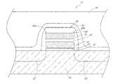
- FIG. 2illustrates an EEPROM transistor 10 in a flash memory cell, constructed in accordance with this preferred embodiment.
- the named process flow stepsare found in FIG. 1 and the numbered structural elements refer to FIG. 2 . It will be understood, however, that elements may differ in appearance during fabrication as compared to the illustrated final structure.
- the gate stack layers described beloware preferably blanket deposited upon one another prior to definition of the gate electrode by photolithography and etch.
- the EEPROM transistor 10 produced by the preferred embodiment of the present inventionis fabricated over a semiconductor substrate 20 , which includes doped regions corresponding to a source 22 and a drain 24 .
- the substrate 20comprises the upper portion of a single-crystal silicon wafer.
- the substratecan comprises any semiconductor structure or layer in which the lowest level of integrated electrical devices are formed.
- a transistor gate structure 26overlies the substrate 20 , particularly over a channel region of the substrate 20 between the source 22 and the drain 24 .
- the active areas 22 , 24 and transistor gate 26together define the EEPROM transistor 10 .
- the first step in the fabrication of the stacked gate structure 26is the formation 110 of an initial dielectric layer 30 on the surface of the substrate 20 .
- the dielectric 30preferably comprises an oxide, and more particularly silicon oxide, though the skilled artisan will appreciate that the present invention will have utility in conjunction with other types of oxide.
- An exemplary alternative oxidecomprises tantalum pentoxide (Ta 2 O 5 ).
- formation 100 of the dielectric 30comprises thermal oxidation of the substrate surface, but persons skilled in the art are able to select an appropriate method of forming the tunnel dielectric layer 30 from the various possible methods.
- the thickness of the illustrated dielectric layer 30is preferably between about 10 ⁇ and 300 ⁇ , more preferably between about 30 ⁇ and 150 ⁇ , and most preferably between about 80 ⁇ and 115 ⁇ (e.g., for a flash memory part).
- the next step shown in FIG. 1comprises nitridation 110 of the initial dielectric layer 30 .
- At least a top surface 40thereby incorporates nitrogen and forms and effective diffusion barrier.
- the amount of nitrogen incorporated into the oxidepreferably forms a barrier to diffusion of hydrogen species out of the dielectric.
- the nitridation 110can be performed either during the growth or in a subsequent anneal of the initial dielectric layer 30 .
- the nitridation 110is performed by exposing the initial dielectric layer 30 to a hydrogen-bearing nitrogen source, particularly ammonia vapor (NH 3 ), while the substrate 20 is held at elevated temperatures.
- a hydrogen-bearing nitrogen sourceparticularly ammonia vapor (NH 3 )
- the amount of nitrogen and hydrogen incorporated in the dielectricincreases with increasing substrate temperature during exposure to NH 3 .
- a substrate temperaturebetween about 850° C. and 950° C. incorporates approximately 2%–3% into the resultant tunnel dielectric 30 , 40 .
- nitrogen and hydrogenare incorporated without nitrogen- or hydrogen-induced defects.
- Conditionsare arranged to incorporate between about 0.1 atomic % and 5.0 atomic % nitrogen in the tunnel dielectric 30 , 40 , more preferably between about 0.1 atomic % and 0.6 atomic %, and most preferably between about 0.3 atomic % and 0.6 atomic %.
- the resultant tunnel dielectric of the illustrated embodimentcomprises silicon oxynitride, or SiO x N y .
- the substrate temperatureis desirably kept below about 850° C. during nitridation 110 , more preferably in the range of about 600° C. to 850° C., and most preferably about 650° C. to 750° C.
- the NH 3 exposure during nitridation 110is preferably maintained for between about 1 second and 60 minutes, more preferably between about 30 seconds and 300 seconds.
- Exemplary pressure during NH 3 nitridation 110for the most preferred temperature range above, is about 300–760 Torr.
- a floating gate 50is formed by depositing a conductive layer (preferably doped polysilicon) onto the tunnel dielectric 30 , 40 . Doping of the polysilicon of the floating gate 50 can be either in situ (i.e., while the floating gate 50 is being formed) or it can be a separate step after the polysilicon deposition. Persons skilled in the art are able to select appropriate materials and methods for creating the floating gate 50 with a particular set of characteristics.
- the formation of the gate stackcontinues by forming a storage dielectric layer 60 on the floating gate 50 .
- the storage dielectric layer 60is composed of oxide-nitride-oxide (ONO), formed by methods known in the art.
- ONOoxide-nitride-oxide
- high dielectric materialscan be employed to improve capacitance of the EEPROM device. Persons skilled in the art can readily select appropriate materials and methods for creating the storage dielectric layer 60 for particular circuit designs.
- the stack completion 120continues by then forming a control gate 70 over the storage dielectric layer 60 .
- the control gate 70can be composed of various conductive materials, including, but not limited to, polysilicon, metal and/or metal silicide.
- a cap insulator layer 80is preferably formed, comprising an insulator such as silicon nitride or silicon oxide, over the control gate 70 .
- the stackis patterned 130 , such as by conventional photolithography and etch processes, to define the gate electrode structure 26 .
- spacers 90 a and 90 bare also formed 140 along the sidewalls of the stacked gate structure 26 .
- Conventional blanket deposition of an insulating material followed by directional spacer etchcan be employed for spacer formation 140 .
- the gate 26 and other surrounding areasare then covered 150 by a substantially conformal liner layer 92 .
- the liner 92 of the preferred embodimentsalso forms a good diffusion barrier against hydroxyl and hydrogen species.
- the liner 92comprises an insulating material, preferably incorporating both silicon and nitrogen.
- preferred liner materialsincludes silicon nitride, silicon oxynitride or a multiple layer laminate including one or both of nitride and oxynitride.
- the inventioncan comprise any of a number of other suitable materials that form effective barriers to diffusion of OH and hydrogen.
- the illustrated liner 92comprises silicon oxynitride (Si x N y O z ), where z is in the range of about zero to 0.3 (30 atomic %), more preferably between about 0.1 and 0.2 and y is greater than zero, more preferably between about 0.3 and 0.57 and most preferably between about 0.4 and 0.57.
- Exemplary ratiosinclude Si 0.43 N 0.57 O 0 (Si 3 N 4 ), Si 0.5 N 0.4 O 0.12 , Si 0.45 N 0.35 O 0.2 , etc.
- the liner 92can be formed 150 by any suitable manner, but is preferably formed by chemical vapor deposition (CVD) to ensure good step coverage over the topography of the patterned gate electrodes 26 across the substrate.
- CVD processesare well developed for each of Si 3 N 4 and silicon oxynitride.
- a silicon sourcee.g., SiH 2 Cl 2
- nitrogen sourcee.g., NH 3
- oxygen sourcee.g., O 2 , N 2 O
- Varying the relative source gas flow or partial pressurecan vary the nitrogen content, as will be appreciated by the skilled artisan.
- CVD oxidecan be nitridized, e.g., by remote plasma nitridation, to incorporate 1–40 atomic % nitrogen, more preferably 4–15 atomic %.
- an interlevel insulating layer 94is deposited 160 over the structure.
- the layer 94serves to electrically isolate underlying devices, such as the EEPROM transistor 10 , from overlying interconnects. Accordingly, the insulating layer 94 is preferably between about 6,000 ⁇ and 20,000 ⁇ in thickness.
- state of the art integrated circuit fabricationtypically employs an alloy step 170 , in which the structure is exposed to a hydrogen-containing ambient at low temperatures (less than about 500° C.).
- the liner 92serves as a barrier to OH and H diffusion.
- such speciescan cause damage to the tunnel oxide 30 in the form of charge leakage paths.
- hydrogen already incorporated into the tunnel oxideprovides passivation of substrate interface.
- the alloy step 170is thus only optional, and can be omitted in the preferred embodiments. If an alloy is employed, the liner 92 advantageously prevents OH and other contamination from reaching the tunnel oxide 30 .
- the integrated circuitis completed by additional fabrication steps. Typically, such steps include metallization processes 180 , interconnecting various devices of the integrated circuit. In order to make contact electrical contact between metal layers and the electronic devices, holes or vias are etched through the interlevel dielectric layers between levels, such as the insulating layer 94 , and then filled with conductors. Contact to the transistor control gate 70 and active areas in the substrate 20 , for example, require contact through the insulating layer 94 and the liner 92 .
- Optional hydrogen anneals 190can also be performed during or after metallization to further reduce the dangling bonds at the substrate surface, including the region of the tunnel dielectric layer 30 , 40 . Diffusion is facilitated somewhat through the contacts. As noted with respect to hydrogen anneal after deposition 160 of the insulating layer 94 , hydrogen diffusion can also be enhanced by grinding the backside of the workpiece.
- the integrated circuitis then completed by formation of bond pads and final passivation 200 , such as by deposition of a further silicon oxynitride layer or other suitable passivation material.
- final passivation 200such as by deposition of a further silicon oxynitride layer or other suitable passivation material.
- the passivation layerforms a seal against moisture or other corrosive agents.
- NH 3during nitridation 110 of the initial dielectric layer 30 advantageously improves the resultant device performance.
- nitridation of the tunnel oxide with hydrogen-bearing speciesenables the use of a more effective diffusion barrier for the liner 92 .
- the more effective liner 92limits exposure of the tunnel oxide 40 to outgassing of OH and H during subsequent processing, which improves data retention in the resultant chip.
- Using NH 3also advantageously provides hydrogen atoms within the tunnel dielectric, preferably resulting in a hydrogen content between about 0.1% and 10% in the tunnel oxide. Moreover, this hydrogen is effectively retained within the tunnel dielectric due to the presence of a nitrogen-rich surface on the tunnel dielectric, locking hydrogen in during subsequent processing.
- the hydrogenis then available at later stages for passivating dangling bonds at the substrate surface and in the region of the tunnel dielectric layer. Because the preferred embodiment of the present invention introduces hydrogen atoms during the formation of the oxynitride layer 40 , the efficacy of any subsequent alloying steps is of less importance. Less aggressive hydrogen anneals can be employed. In one embodiment, subsequent hydrogen anneals are eliminated altogether. In another embodiment, only post-metallization hydrogen anneal is employed.
- the use of NH 3 for nitridationpermits the use of a more effective diffusion barrier for the liner layer 100 that protects the transistor gate stack.
- very effective diffusion barriersprotect the transistor from water or OH contamination during BPSG deposition, for example, they also inhibit desirable hydrogen diffusion.
- the preferred embodimentsprovide and seal hydrogen in the tunnel dielectric at an early stage, thereby facilitating use of more effective liner material without sacrificing hydrogen passivation of the tunnel dielectric and substrate interface.
- the liner layer 100comprises silicon nitride (Si 3 N 4 ) or silicon oxynitride (SiO x N y ). These nitrogen-containing compounds are more effective barriers to OH diffusion than, for example, LPCVD oxide.
Landscapes
- Engineering & Computer Science (AREA)
- Condensed Matter Physics & Semiconductors (AREA)
- Manufacturing & Machinery (AREA)
- General Chemical & Material Sciences (AREA)
- Physics & Mathematics (AREA)
- Chemical Kinetics & Catalysis (AREA)
- Chemical & Material Sciences (AREA)
- General Physics & Mathematics (AREA)
- Crystallography & Structural Chemistry (AREA)
- Computer Hardware Design (AREA)
- Microelectronics & Electronic Packaging (AREA)
- Power Engineering (AREA)
- Non-Volatile Memory (AREA)
- Semiconductor Memories (AREA)
- Formation Of Insulating Films (AREA)
Abstract
Description
Claims (18)
Priority Applications (1)
| Application Number | Priority Date | Filing Date | Title |
|---|---|---|---|
| US10/378,354US7087182B2 (en) | 2000-04-06 | 2003-03-03 | Process of forming an electrically erasable programmable read only memory with an oxide layer exposed to hydrogen and nitrogen |
Applications Claiming Priority (2)
| Application Number | Priority Date | Filing Date | Title |
|---|---|---|---|
| US09/544,505US6559007B1 (en) | 2000-04-06 | 2000-04-06 | Method for forming flash memory device having a tunnel dielectric comprising nitrided oxide |
| US10/378,354US7087182B2 (en) | 2000-04-06 | 2003-03-03 | Process of forming an electrically erasable programmable read only memory with an oxide layer exposed to hydrogen and nitrogen |
Related Parent Applications (1)
| Application Number | Title | Priority Date | Filing Date |
|---|---|---|---|
| US09/544,505DivisionUS6559007B1 (en) | 2000-04-06 | 2000-04-06 | Method for forming flash memory device having a tunnel dielectric comprising nitrided oxide |
Publications (2)
| Publication Number | Publication Date |
|---|---|
| US20030157807A1 US20030157807A1 (en) | 2003-08-21 |
| US7087182B2true US7087182B2 (en) | 2006-08-08 |
Family
ID=24172450
Family Applications (5)
| Application Number | Title | Priority Date | Filing Date |
|---|---|---|---|
| US09/544,505Expired - Fee RelatedUS6559007B1 (en) | 2000-04-06 | 2000-04-06 | Method for forming flash memory device having a tunnel dielectric comprising nitrided oxide |
| US10/378,568Expired - LifetimeUS6924197B2 (en) | 2000-04-06 | 2003-03-03 | Method of fabricating an integrated circuit with a dielectric layer exposed to a hydrogen-bearing nitrogen source |
| US10/378,354Expired - LifetimeUS7087182B2 (en) | 2000-04-06 | 2003-03-03 | Process of forming an electrically erasable programmable read only memory with an oxide layer exposed to hydrogen and nitrogen |
| US10/378,573Expired - LifetimeUS6921937B2 (en) | 2000-04-06 | 2003-03-03 | Integrated circuit with a dielectric layer exposed to a hydrogen-bearing nitrogen source |
| US10/758,518Expired - Fee RelatedUS6815805B2 (en) | 2000-04-06 | 2004-01-15 | Method of fabricating an integrated circuit with a dielectric layer exposed to a hydrogen-bearing nitrogen source |
Family Applications Before (2)
| Application Number | Title | Priority Date | Filing Date |
|---|---|---|---|
| US09/544,505Expired - Fee RelatedUS6559007B1 (en) | 2000-04-06 | 2000-04-06 | Method for forming flash memory device having a tunnel dielectric comprising nitrided oxide |
| US10/378,568Expired - LifetimeUS6924197B2 (en) | 2000-04-06 | 2003-03-03 | Method of fabricating an integrated circuit with a dielectric layer exposed to a hydrogen-bearing nitrogen source |
Family Applications After (2)
| Application Number | Title | Priority Date | Filing Date |
|---|---|---|---|
| US10/378,573Expired - LifetimeUS6921937B2 (en) | 2000-04-06 | 2003-03-03 | Integrated circuit with a dielectric layer exposed to a hydrogen-bearing nitrogen source |
| US10/758,518Expired - Fee RelatedUS6815805B2 (en) | 2000-04-06 | 2004-01-15 | Method of fabricating an integrated circuit with a dielectric layer exposed to a hydrogen-bearing nitrogen source |
Country Status (1)
| Country | Link |
|---|---|
| US (5) | US6559007B1 (en) |
Cited By (2)
| Publication number | Priority date | Publication date | Assignee | Title |
|---|---|---|---|---|
| US20070134867A1 (en)* | 2005-12-14 | 2007-06-14 | Freescale Semiconductor, Inc. | Floating gate non-volatile memory and method thereof |
| US20080025087A1 (en)* | 2006-07-27 | 2008-01-31 | Macronix International Co., Ltd. | Method for fabricating charge-trapping memory |
Families Citing this family (70)
| Publication number | Priority date | Publication date | Assignee | Title |
|---|---|---|---|---|
| US6559007B1 (en)* | 2000-04-06 | 2003-05-06 | Micron Technology, Inc. | Method for forming flash memory device having a tunnel dielectric comprising nitrided oxide |
| US6544908B1 (en)* | 2000-08-30 | 2003-04-08 | Micron Technology, Inc. | Ammonia gas passivation on nitride encapsulated devices |
| US6750157B1 (en)* | 2000-10-12 | 2004-06-15 | Advanced Micro Devices, Inc. | Nonvolatile memory cell with a nitridated oxide layer |
| KR20020093223A (en)* | 2001-06-07 | 2002-12-16 | 삼성전자 주식회사 | Non volatile memory device and method of fabricating the same |
| DE10228768A1 (en)* | 2001-06-28 | 2003-01-16 | Samsung Electronics Co Ltd | Non-volatile floating trap storage device comprises a semiconductor substrate, a tunnel insulation layer on the substrate, a charge storage layer, a barrier insulation layer, and a gate electrode |
| US20030040171A1 (en)* | 2001-08-22 | 2003-02-27 | Weimer Ronald A. | Method of composite gate formation |
| KR100399952B1 (en)* | 2001-11-16 | 2003-09-29 | 주식회사 하이닉스반도체 | Method of image sensor for reducing dark current |
| FR2838554B1 (en)* | 2002-04-15 | 2004-07-09 | St Microelectronics Sa | NON-VOLATILE, PROGRAMMABLE AND ELECTRICALLY ERASABLE MEMORY CONDUCTOR WITH A SINGLE LAYER OF GRID MATERIAL, AND CORRESPONDING MEMORY PLAN |
| US8080453B1 (en) | 2002-06-28 | 2011-12-20 | Cypress Semiconductor Corporation | Gate stack having nitride layer |
| US7256083B1 (en)* | 2002-06-28 | 2007-08-14 | Cypress Semiconductor Corporation | Nitride layer on a gate stack |
| US6828623B1 (en)* | 2002-08-30 | 2004-12-07 | Advanced Micro Devices, Inc. | Floating gate memory device with homogeneous oxynitride tunneling dielectric |
| US7192892B2 (en) | 2003-03-04 | 2007-03-20 | Micron Technology, Inc. | Atomic layer deposited dielectric layers |
| US7098589B2 (en)* | 2003-04-15 | 2006-08-29 | Luminus Devices, Inc. | Light emitting devices with high light collimation |
| US20040256671A1 (en)* | 2003-06-17 | 2004-12-23 | Kuo-Tai Huang | Metal-oxide-semiconductor transistor with selective epitaxial growth film |
| US7060554B2 (en)* | 2003-07-11 | 2006-06-13 | Advanced Micro Devices, Inc. | PECVD silicon-rich oxide layer for reduced UV charging |
| US7371637B2 (en)* | 2003-09-26 | 2008-05-13 | Cypress Semiconductor Corporation | Oxide-nitride stack gate dielectric |
| US7183143B2 (en)* | 2003-10-27 | 2007-02-27 | Macronix International Co., Ltd. | Method for forming nitrided tunnel oxide layer |
| US7166525B2 (en)* | 2004-01-15 | 2007-01-23 | Taiwan Semiconductor Manufacturing Company, Ltd. | High temperature hydrogen annealing of a gate insulator layer to increase etching selectivity between conductive gate structure and gate insulator layer |
| JP2005311300A (en)* | 2004-03-26 | 2005-11-04 | Toshiba Corp | Semiconductor memory device and manufacturing method thereof |
| US7349079B2 (en)* | 2004-05-14 | 2008-03-25 | Kla-Tencor Technologies Corp. | Methods for measurement or analysis of a nitrogen concentration of a specimen |
| US7564552B2 (en)* | 2004-05-14 | 2009-07-21 | Kla-Tencor Technologies Corp. | Systems and methods for measurement of a specimen with vacuum ultraviolet light |
| US7359052B2 (en)* | 2004-05-14 | 2008-04-15 | Kla-Tencor Technologies Corp. | Systems and methods for measurement of a specimen with vacuum ultraviolet light |
| US7067819B2 (en)* | 2004-05-14 | 2006-06-27 | Kla-Tencor Technologies Corp. | Systems and methods for measurement or analysis of a specimen using separated spectral peaks in light |
| US7405125B2 (en)* | 2004-06-01 | 2008-07-29 | Macronix International Co., Ltd. | Tunnel oxynitride in flash memories |
| US7488690B2 (en)* | 2004-07-06 | 2009-02-10 | Applied Materials, Inc. | Silicon nitride film with stress control |
| KR100575343B1 (en)* | 2004-09-10 | 2006-05-02 | 주식회사 하이닉스반도체 | Manufacturing Method of Flash Memory Device |
| JP4579637B2 (en)* | 2004-10-01 | 2010-11-10 | 東京エレクトロン株式会社 | Semiconductor memory device and manufacturing method thereof |
| KR100688575B1 (en)* | 2004-10-08 | 2007-03-02 | 삼성전자주식회사 | Nonvolatile Semiconductor Memory Devices |
| US7060594B2 (en)* | 2004-10-19 | 2006-06-13 | Macronix International Co., Ltd. | Memory device and method of manufacturing including deuterated oxynitride charge trapping structure |
| KR100597649B1 (en)* | 2004-11-26 | 2006-07-05 | 삼성전자주식회사 | Method for fabricating semiconductor device comprising barrier metal and its structure |
| JP2006186245A (en)* | 2004-12-28 | 2006-07-13 | Tokyo Electron Ltd | Method of nitriding tunnel oxide film, method of manufacturing nonvolatile memory element, nonvolatile memory element, computer program, and recording medium |
| US8482052B2 (en) | 2005-01-03 | 2013-07-09 | Macronix International Co., Ltd. | Silicon on insulator and thin film transistor bandgap engineered split gate memory |
| US7315474B2 (en) | 2005-01-03 | 2008-01-01 | Macronix International Co., Ltd | Non-volatile memory cells, memory arrays including the same and methods of operating cells and arrays |
| US7473589B2 (en) | 2005-12-09 | 2009-01-06 | Macronix International Co., Ltd. | Stacked thin film transistor, non-volatile memory devices and methods for fabricating the same |
| US7642585B2 (en)* | 2005-01-03 | 2010-01-05 | Macronix International Co., Ltd. | Non-volatile memory cells, memory arrays including the same and methods of operating cells and arrays |
| KR100623177B1 (en)* | 2005-01-25 | 2006-09-13 | 삼성전자주식회사 | Dielectric structure having high dielectric constant, manufacturing method thereof, nonvolatile semiconductor memory device comprising same and manufacturing method thereof |
| US7408641B1 (en) | 2005-02-14 | 2008-08-05 | Kla-Tencor Technologies Corp. | Measurement systems configured to perform measurements of a specimen and illumination subsystems configured to provide illumination for a measurement system |
| US7399666B2 (en)* | 2005-02-15 | 2008-07-15 | Micron Technology, Inc. | Atomic layer deposition of Zr3N4/ZrO2 films as gate dielectrics |
| US7498247B2 (en)* | 2005-02-23 | 2009-03-03 | Micron Technology, Inc. | Atomic layer deposition of Hf3N4/HfO2 films as gate dielectrics |
| KR100676599B1 (en)* | 2005-02-28 | 2007-01-30 | 주식회사 하이닉스반도체 | Manufacturing Method of Flash Memory Device |
| US7356229B2 (en) | 2005-02-28 | 2008-04-08 | 3M Innovative Properties Company | Reflective polarizers containing polymer fibers |
| KR100644397B1 (en)* | 2005-04-07 | 2006-11-10 | 삼성전자주식회사 | Thin film processing method and manufacturing method of nonvolatile memory cell using same |
| US7287325B2 (en)* | 2005-05-10 | 2007-10-30 | International Business Machines Corporation | Method of forming interconnect structure or interconnect and via structures using post chemical mechanical polishing |
| US7212457B2 (en)* | 2005-05-18 | 2007-05-01 | Macronix International Co., Ltd. | Method and apparatus for implementing high speed memory |
| US7790561B2 (en)* | 2005-07-01 | 2010-09-07 | Texas Instruments Incorporated | Gate sidewall spacer and method of manufacture therefor |
| US7763927B2 (en) | 2005-12-15 | 2010-07-27 | Macronix International Co., Ltd. | Non-volatile memory device having a nitride-oxide dielectric layer |
| US8110469B2 (en) | 2005-08-30 | 2012-02-07 | Micron Technology, Inc. | Graded dielectric layers |
| KR100729354B1 (en)* | 2005-12-07 | 2007-06-15 | 삼성전자주식회사 | Manufacturing Method of Semiconductor Device for Improving Electrical Properties of Dielectric Film |
| US7473636B2 (en)* | 2006-01-12 | 2009-01-06 | International Business Machines Corporation | Method to improve time dependent dielectric breakdown |
| US7907450B2 (en) | 2006-05-08 | 2011-03-15 | Macronix International Co., Ltd. | Methods and apparatus for implementing bit-by-bit erase of a flash memory device |
| US8153502B2 (en)* | 2006-05-16 | 2012-04-10 | Micron Technology, Inc. | Methods for filling trenches in a semiconductor material |
| US8772858B2 (en) | 2006-10-11 | 2014-07-08 | Macronix International Co., Ltd. | Vertical channel memory and manufacturing method thereof and operating method using the same |
| US7811890B2 (en) | 2006-10-11 | 2010-10-12 | Macronix International Co., Ltd. | Vertical channel transistor structure and manufacturing method thereof |
| US8252640B1 (en) | 2006-11-02 | 2012-08-28 | Kapre Ravindra M | Polycrystalline silicon activation RTA |
| US8415734B2 (en)* | 2006-12-07 | 2013-04-09 | Spansion Llc | Memory device protection layer |
| KR20090013474A (en)* | 2007-08-02 | 2009-02-05 | 삼성전자주식회사 | Manufacturing method of nonvolatile memory device |
| US7737488B2 (en) | 2007-08-09 | 2010-06-15 | Macronix International Co., Ltd. | Blocking dielectric engineered charge trapping memory cell with high speed erase |
| JP5518366B2 (en)* | 2008-05-16 | 2014-06-11 | 株式会社半導体エネルギー研究所 | Thin film transistor |
| US20090321809A1 (en)* | 2008-06-30 | 2009-12-31 | Nirmal Ramaswamy | Graded oxy-nitride tunnel barrier |
| US20100117141A1 (en)* | 2008-11-13 | 2010-05-13 | Samsung Electronics Co., Ltd. | Memory cell transistors having limited charge spreading, non-volatile memory devices including such transistors, and methods of formation thereof |
| JP4902716B2 (en)* | 2008-11-20 | 2012-03-21 | 株式会社日立国際電気 | Nonvolatile semiconductor memory device and manufacturing method thereof |
| US8644046B2 (en) | 2009-02-10 | 2014-02-04 | Samsung Electronics Co., Ltd. | Non-volatile memory devices including vertical NAND channels and methods of forming the same |
| US8614917B2 (en) | 2010-02-05 | 2013-12-24 | Samsung Electronics Co., Ltd. | Vertically-integrated nonvolatile memory devices having laterally-integrated ground select transistors |
| US9240405B2 (en) | 2011-04-19 | 2016-01-19 | Macronix International Co., Ltd. | Memory with off-chip controller |
| US10629749B2 (en)* | 2017-11-30 | 2020-04-21 | Taiwan Semiconductor Manufacturing Co., Ltd. | Method of treating interfacial layer on silicon germanium |
| JP7177260B2 (en) | 2018-10-09 | 2022-11-22 | マイクロン テクノロジー,インク. | Device and associated method including vertical transistor with hydrogen barrier material |
| EP3864704A4 (en) | 2018-10-09 | 2022-10-12 | Micron Technology, Inc. | VERTICAL TRANSISTOR DEVICES AND ELECTRONIC SYSTEMS AND RELATED METHODS |
| CN112930600B (en) | 2018-10-09 | 2023-12-01 | 美光科技公司 | Devices including vertical transistors and related methods |
| TWI685085B (en)* | 2019-02-26 | 2020-02-11 | 華邦電子股份有限公司 | Memory device and method of manufacturing the same |
| US11594644B2 (en) | 2019-11-13 | 2023-02-28 | Micron Technology, Inc. | Microelectronic devices including passivation materials, related electronic devices, and related methods |
Citations (66)
| Publication number | Priority date | Publication date | Assignee | Title |
|---|---|---|---|---|
| US4142004A (en) | 1976-01-22 | 1979-02-27 | Bell Telephone Laboratories, Incorporated | Method of coating semiconductor substrates |
| US4432035A (en)* | 1982-06-11 | 1984-02-14 | International Business Machines Corp. | Method of making high dielectric constant insulators and capacitors using same |
| US4551231A (en) | 1981-10-13 | 1985-11-05 | Ashland Oil, Inc. | Ammonia contacting to passivate metals deposited on a cracking catalyst during reduced crude processing |
| US4581622A (en)* | 1979-09-14 | 1986-04-08 | Fujitsu Limited | UV erasable EPROM with UV transparent silicon oxynitride coating |
| US4621277A (en)* | 1978-06-14 | 1986-11-04 | Fujitsu Limited | Semiconductor device having insulating film |
| US4623912A (en) | 1984-12-05 | 1986-11-18 | At&T Bell Laboratories | Nitrided silicon dioxide layers for semiconductor integrated circuits |
| US4814292A (en) | 1986-07-02 | 1989-03-21 | Oki Electric Industry Co., Ltd. | Process of fabricating a semiconductor device involving densification and recrystallization of amorphous silicon |
| US4872043A (en) | 1985-06-21 | 1989-10-03 | Texas Instruments Incorporated | Charge coupled device with reduced surface state at semiconductor-insulator interface |
| US5102832A (en) | 1991-02-11 | 1992-04-07 | Micron Technology, Inc. | Methods for texturizing polysilicon |
| US5112773A (en) | 1991-04-10 | 1992-05-12 | Micron Technology, Inc. | Methods for texturizing polysilicon utilizing gas phase nucleation |
| US5159430A (en) | 1991-07-24 | 1992-10-27 | Micron Technology, Inc. | Vertically integrated oxygen-implanted polysilicon resistor |
| US5247199A (en)* | 1986-01-15 | 1993-09-21 | Harris Corporation | Process for forming twin well CMOS integrated circuits |
| US5264724A (en) | 1989-02-13 | 1993-11-23 | The University Of Arkansas | Silicon nitride for application as the gate dielectric in MOS devices |
| US5288527A (en) | 1990-09-03 | 1994-02-22 | Saint Gobain Vitrage International C/O Saint Gobain Recherche | Silicon nitride thin films with improved properties |
| US5352330A (en) | 1992-09-30 | 1994-10-04 | Texas Instruments Incorporated | Process for producing nanometer-size structures on surfaces using electron beam induced chemistry through electron stimulated desorption |
| US5366917A (en) | 1990-03-20 | 1994-11-22 | Nec Corporation | Method for fabricating polycrystalline silicon having micro roughness on the surface |
| US5385863A (en) | 1991-06-21 | 1995-01-31 | Nec Corporation | Method of manufacturing polysilicon film including recrystallization of an amorphous film |
| US5397720A (en) | 1994-01-07 | 1995-03-14 | The Regents Of The University Of Texas System | Method of making MOS transistor having improved oxynitride dielectric |
| US5420056A (en)* | 1994-01-14 | 1995-05-30 | Texas Instruments Incorporated | Junction contact process and structure for semiconductor technologies |
| US5445999A (en) | 1992-11-13 | 1995-08-29 | Micron Technology, Inc. | Advanced technique to improve the bonding arrangement on silicon surfaces to promote uniform nitridation |
| US5462898A (en) | 1994-05-25 | 1995-10-31 | Georgia Tech Research Corporation | Methods for passivating silicon devices at low temperature to achieve low interface state density and low recombination velocity while preserving carrier lifetime |
| US5489542A (en) | 1990-11-28 | 1996-02-06 | Kabushiki Kaisha Toshiba | Method for fabricating semiconductor device in which threshold voltage shift and charge-pumping current are improved |
| US5521127A (en)* | 1987-07-31 | 1996-05-28 | Matsushita Electric Industrial Co., Ltd. | Re-oxidized nitrided oxides and re-annealed nitrided oxides prepared by rapid thermal processing |
| US5707898A (en) | 1996-04-01 | 1998-01-13 | Micron Technology, Inc. | Method of forming a programmable non-volatile memory cell by providing a shielding layer over the gate sidewalls |
| US5707746A (en) | 1992-09-25 | 1998-01-13 | Sharp Kabushiki Kaisha | Thin film transistor device with advanced characteristics by improved matching between a glass substrate and a silicon nitride layer |
| US5711998A (en) | 1996-05-31 | 1998-01-27 | Lam Research Corporation | Method of polycrystalline silicon hydrogenation |
| US5821603A (en) | 1996-05-29 | 1998-10-13 | Microunity Systems Engineering, Inc. | Method for depositing double nitride layer in semiconductor processing |
| US5825046A (en)* | 1996-10-28 | 1998-10-20 | Energy Conversion Devices, Inc. | Composite memory material comprising a mixture of phase-change memory material and dielectric material |
| US5880008A (en) | 1995-10-18 | 1999-03-09 | Sharp Kabushiki Kaisha | Method for forming field oxide film |
| US5904860A (en) | 1995-09-12 | 1999-05-18 | Nippondenso Co., Ltd. | Method for direct bonding nitride bodies |
| US5936291A (en) | 1997-02-03 | 1999-08-10 | Sharp Kabushiki Kaisha | Thin film transistor and method for fabricating the same |
| US5946542A (en) | 1996-02-26 | 1999-08-31 | Micron Technology, Inc. | Method of depositing passivation layers on semiconductor device arrays |
| US5972804A (en) | 1997-08-05 | 1999-10-26 | Motorola, Inc. | Process for forming a semiconductor device |
| US5972765A (en) | 1997-07-16 | 1999-10-26 | International Business Machines Corporation | Use of deuterated materials in semiconductor processing |
| US6017784A (en) | 1996-06-09 | 2000-01-25 | Fujitsu Limited | Manufacture method of semiconductor device with suppressed impurity diffusion from gate electrode |
| US6017808A (en) | 1997-10-24 | 2000-01-25 | Lsi Logic Corporation | Nitrogen implanted polysilicon gate for MOSFET gate oxide hardening |
| US6025281A (en) | 1997-12-18 | 2000-02-15 | Motorola, Inc. | Passivation of oxide-compound semiconductor interfaces |
| US6048795A (en) | 1994-11-04 | 2000-04-11 | Nec Corporation | Process of fabricating a semiconductor device having nitrogen-containing silicon layer and refractory metal layer |
| US6060954A (en) | 1997-11-28 | 2000-05-09 | Delta Electronic, Inc. | Oscillator device having inductor formed inside multi-layer circuit board |
| US6087206A (en) | 1994-11-22 | 2000-07-11 | Nec Corporation | Method of fabricating a top-gate type thin film transistor with dangling bonds of silicon partly combined with hydrogen |
| US6136641A (en) | 1997-08-14 | 2000-10-24 | Samsung Electronics, Co., Ltd. | Method for manufacturing capacitor of semiconductor device including thermal treatment to dielectric film under hydrogen atmosphere |
| US6143608A (en) | 1999-03-31 | 2000-11-07 | Advanced Micro Devices, Inc. | Barrier layer decreases nitrogen contamination of peripheral gate regions during tunnel oxide nitridation |
| US6147014A (en) | 1996-01-16 | 2000-11-14 | The Board Of Trustees, University Of Illinois, Urbana | Forming of deuterium containing nitride spacers and fabrication of semiconductor devices |
| US6150725A (en) | 1997-02-27 | 2000-11-21 | Sanyo Electric Co., Ltd. | Semiconductor devices with means to reduce contamination |
| US6197701B1 (en) | 1998-10-23 | 2001-03-06 | Taiwan Semiconductor Manufacturing Company | Lightly nitridation surface for preparing thin-gate oxides |
| US6204203B1 (en) | 1998-10-14 | 2001-03-20 | Applied Materials, Inc. | Post deposition treatment of dielectric films for interface control |
| US6248673B1 (en) | 2000-02-23 | 2001-06-19 | Taiwan Semiconductor Manufacturing Company, Ltd. | Hydrogen thermal annealing method for stabilizing microelectronic devices |
| US6251726B1 (en) | 2000-01-21 | 2001-06-26 | Taiwan Semiconductor Manufacturing Company | Method for making an enlarged DRAM capacitor using an additional polysilicon plug as a center pillar |
| US6255230B1 (en) | 1999-06-04 | 2001-07-03 | Canon Sales Co., Inc. | Method for modifying a film forming surface of a substrate on which a film is to be formed, and method for manufacturing a semiconductor device using the same |
| US6258730B1 (en) | 1999-02-09 | 2001-07-10 | Advanced Micro Devices, Inc. | Ultra-thin gate oxide formation using an N2O plasma |
| US6265327B1 (en) | 1997-06-20 | 2001-07-24 | Japan Science And Technology Corp. | Method for forming an insulating film on semiconductor substrate surface and apparatus for carrying out the method |
| US6274442B1 (en) | 1998-07-15 | 2001-08-14 | Advanced Micro Devices, Inc. | Transistor having a nitrogen incorporated epitaxially grown gate dielectric and method of making same |
| US6278166B1 (en) | 1997-12-12 | 2001-08-21 | Advanced Micro Devices, Inc. | Use of nitric oxide surface anneal to provide reaction barrier for deposition of tantalum pentoxide |
| US6284583B1 (en) | 1997-06-30 | 2001-09-04 | Kabushiki Kaisha Toshiba | Semiconductor device and method of manufacturing the same |
| US6316354B1 (en) | 1999-10-26 | 2001-11-13 | Lsi Logic Corporation | Process for removing resist mask of integrated circuit structure which mitigates damage to underlying low dielectric constant silicon oxide dielectric layer |
| US6323519B1 (en) | 1998-10-23 | 2001-11-27 | Advanced Micro Devices, Inc. | Ultrathin, nitrogen-containing MOSFET sidewall spacers using low-temperature semiconductor fabrication process |
| US6348380B1 (en) | 2000-08-25 | 2002-02-19 | Micron Technology, Inc. | Use of dilute steam ambient for improvement of flash devices |
| US6387761B1 (en) | 1998-09-14 | 2002-05-14 | Applied Materials, Inc. | Anneal for enhancing the electrical characteristic of semiconductor devices |
| US6420752B1 (en) | 2000-02-11 | 2002-07-16 | Advanced Micro Devices, Inc. | Semiconductor device with self-aligned contacts using a liner oxide layer |
| US6465370B1 (en) | 1998-06-26 | 2002-10-15 | Infineon Technologies Ag | Low leakage, low capacitance isolation material |
| US6482477B1 (en) | 2000-11-28 | 2002-11-19 | Tokyo Electron Limited | Method for pretreating dielectric layers to enhance the adhesion of CVD metal layers thereto |
| US6483172B1 (en) | 1998-03-09 | 2002-11-19 | Siemens Aktiengesellschaft | Semiconductor device structure with hydrogen-rich layer for facilitating passivation of surface states |
| US6485988B2 (en) | 1999-12-22 | 2002-11-26 | Texas Instruments Incorporated | Hydrogen-free contact etch for ferroelectric capacitor formation |
| US6544908B1 (en) | 2000-08-30 | 2003-04-08 | Micron Technology, Inc. | Ammonia gas passivation on nitride encapsulated devices |
| US6551867B1 (en) | 1999-01-25 | 2003-04-22 | Sanyo Electric Co., Ltd. | Non-volatile semiconductor memory device and method for manufacturing the same |
| US6559007B1 (en) | 2000-04-06 | 2003-05-06 | Micron Technology, Inc. | Method for forming flash memory device having a tunnel dielectric comprising nitrided oxide |
Family Cites Families (2)
| Publication number | Priority date | Publication date | Assignee | Title |
|---|---|---|---|---|
| US6218720B1 (en)* | 1998-10-21 | 2001-04-17 | Advanced Micro Devices, Inc. | Semiconductor topography employing a nitrogenated shallow trench isolation structure |
| US6653222B2 (en)* | 1999-08-03 | 2003-11-25 | International Business Machines Corporation | Plasma enhanced liner |
- 2000
- 2000-04-06USUS09/544,505patent/US6559007B1/ennot_activeExpired - Fee Related
- 2003
- 2003-03-03USUS10/378,568patent/US6924197B2/ennot_activeExpired - Lifetime
- 2003-03-03USUS10/378,354patent/US7087182B2/ennot_activeExpired - Lifetime
- 2003-03-03USUS10/378,573patent/US6921937B2/ennot_activeExpired - Lifetime
- 2004
- 2004-01-15USUS10/758,518patent/US6815805B2/ennot_activeExpired - Fee Related
Patent Citations (70)
| Publication number | Priority date | Publication date | Assignee | Title |
|---|---|---|---|---|
| US4142004A (en) | 1976-01-22 | 1979-02-27 | Bell Telephone Laboratories, Incorporated | Method of coating semiconductor substrates |
| US4621277A (en)* | 1978-06-14 | 1986-11-04 | Fujitsu Limited | Semiconductor device having insulating film |
| US4581622A (en)* | 1979-09-14 | 1986-04-08 | Fujitsu Limited | UV erasable EPROM with UV transparent silicon oxynitride coating |
| US4551231A (en) | 1981-10-13 | 1985-11-05 | Ashland Oil, Inc. | Ammonia contacting to passivate metals deposited on a cracking catalyst during reduced crude processing |
| US4432035A (en)* | 1982-06-11 | 1984-02-14 | International Business Machines Corp. | Method of making high dielectric constant insulators and capacitors using same |
| US4623912A (en) | 1984-12-05 | 1986-11-18 | At&T Bell Laboratories | Nitrided silicon dioxide layers for semiconductor integrated circuits |
| US4872043A (en) | 1985-06-21 | 1989-10-03 | Texas Instruments Incorporated | Charge coupled device with reduced surface state at semiconductor-insulator interface |
| US5247199A (en)* | 1986-01-15 | 1993-09-21 | Harris Corporation | Process for forming twin well CMOS integrated circuits |
| US4814292A (en) | 1986-07-02 | 1989-03-21 | Oki Electric Industry Co., Ltd. | Process of fabricating a semiconductor device involving densification and recrystallization of amorphous silicon |
| US5521127A (en)* | 1987-07-31 | 1996-05-28 | Matsushita Electric Industrial Co., Ltd. | Re-oxidized nitrided oxides and re-annealed nitrided oxides prepared by rapid thermal processing |
| US5264724A (en) | 1989-02-13 | 1993-11-23 | The University Of Arkansas | Silicon nitride for application as the gate dielectric in MOS devices |
| US5366917A (en) | 1990-03-20 | 1994-11-22 | Nec Corporation | Method for fabricating polycrystalline silicon having micro roughness on the surface |
| US5288527A (en) | 1990-09-03 | 1994-02-22 | Saint Gobain Vitrage International C/O Saint Gobain Recherche | Silicon nitride thin films with improved properties |
| US5489542A (en) | 1990-11-28 | 1996-02-06 | Kabushiki Kaisha Toshiba | Method for fabricating semiconductor device in which threshold voltage shift and charge-pumping current are improved |
| US5102832A (en) | 1991-02-11 | 1992-04-07 | Micron Technology, Inc. | Methods for texturizing polysilicon |
| US5112773A (en) | 1991-04-10 | 1992-05-12 | Micron Technology, Inc. | Methods for texturizing polysilicon utilizing gas phase nucleation |
| US5385863A (en) | 1991-06-21 | 1995-01-31 | Nec Corporation | Method of manufacturing polysilicon film including recrystallization of an amorphous film |
| US5159430A (en) | 1991-07-24 | 1992-10-27 | Micron Technology, Inc. | Vertically integrated oxygen-implanted polysilicon resistor |
| US6013310A (en) | 1992-09-25 | 2000-01-11 | Sharp Kabushiki Kaisha | Method for producing a thin film semiconductor device |
| US5707746A (en) | 1992-09-25 | 1998-01-13 | Sharp Kabushiki Kaisha | Thin film transistor device with advanced characteristics by improved matching between a glass substrate and a silicon nitride layer |
| US5352330A (en) | 1992-09-30 | 1994-10-04 | Texas Instruments Incorporated | Process for producing nanometer-size structures on surfaces using electron beam induced chemistry through electron stimulated desorption |
| US5445999A (en) | 1992-11-13 | 1995-08-29 | Micron Technology, Inc. | Advanced technique to improve the bonding arrangement on silicon surfaces to promote uniform nitridation |
| US5397720A (en) | 1994-01-07 | 1995-03-14 | The Regents Of The University Of Texas System | Method of making MOS transistor having improved oxynitride dielectric |
| US5420056A (en)* | 1994-01-14 | 1995-05-30 | Texas Instruments Incorporated | Junction contact process and structure for semiconductor technologies |
| US5462898A (en) | 1994-05-25 | 1995-10-31 | Georgia Tech Research Corporation | Methods for passivating silicon devices at low temperature to achieve low interface state density and low recombination velocity while preserving carrier lifetime |
| US6048795A (en) | 1994-11-04 | 2000-04-11 | Nec Corporation | Process of fabricating a semiconductor device having nitrogen-containing silicon layer and refractory metal layer |
| US6087206A (en) | 1994-11-22 | 2000-07-11 | Nec Corporation | Method of fabricating a top-gate type thin film transistor with dangling bonds of silicon partly combined with hydrogen |
| US5904860A (en) | 1995-09-12 | 1999-05-18 | Nippondenso Co., Ltd. | Method for direct bonding nitride bodies |
| US5880008A (en) | 1995-10-18 | 1999-03-09 | Sharp Kabushiki Kaisha | Method for forming field oxide film |
| US6444533B1 (en) | 1996-01-16 | 2002-09-03 | Board Of Trustees Of The University Of Illinois | Semiconductor devices and methods for same |
| US6147014A (en) | 1996-01-16 | 2000-11-14 | The Board Of Trustees, University Of Illinois, Urbana | Forming of deuterium containing nitride spacers and fabrication of semiconductor devices |
| US5946542A (en) | 1996-02-26 | 1999-08-31 | Micron Technology, Inc. | Method of depositing passivation layers on semiconductor device arrays |
| US5726471A (en)* | 1996-04-01 | 1998-03-10 | Micron Technology, Inc. | Programmable non-volatile memory cell and method of forming a programmable non-volatile memory cell |
| US5707898A (en) | 1996-04-01 | 1998-01-13 | Micron Technology, Inc. | Method of forming a programmable non-volatile memory cell by providing a shielding layer over the gate sidewalls |
| US5821603A (en) | 1996-05-29 | 1998-10-13 | Microunity Systems Engineering, Inc. | Method for depositing double nitride layer in semiconductor processing |
| US5711998A (en) | 1996-05-31 | 1998-01-27 | Lam Research Corporation | Method of polycrystalline silicon hydrogenation |
| US6017784A (en) | 1996-06-09 | 2000-01-25 | Fujitsu Limited | Manufacture method of semiconductor device with suppressed impurity diffusion from gate electrode |
| US6380014B1 (en) | 1996-09-06 | 2002-04-30 | Fujitsu Limited | Manufacture method of semiconductor device with suppressed impurity diffusion from gate electrode |
| US5825046A (en)* | 1996-10-28 | 1998-10-20 | Energy Conversion Devices, Inc. | Composite memory material comprising a mixture of phase-change memory material and dielectric material |
| US5936291A (en) | 1997-02-03 | 1999-08-10 | Sharp Kabushiki Kaisha | Thin film transistor and method for fabricating the same |
| US6150725A (en) | 1997-02-27 | 2000-11-21 | Sanyo Electric Co., Ltd. | Semiconductor devices with means to reduce contamination |
| US6265327B1 (en) | 1997-06-20 | 2001-07-24 | Japan Science And Technology Corp. | Method for forming an insulating film on semiconductor substrate surface and apparatus for carrying out the method |
| US6284583B1 (en) | 1997-06-30 | 2001-09-04 | Kabushiki Kaisha Toshiba | Semiconductor device and method of manufacturing the same |
| US5972765A (en) | 1997-07-16 | 1999-10-26 | International Business Machines Corporation | Use of deuterated materials in semiconductor processing |
| US5972804A (en) | 1997-08-05 | 1999-10-26 | Motorola, Inc. | Process for forming a semiconductor device |
| US6136641A (en) | 1997-08-14 | 2000-10-24 | Samsung Electronics, Co., Ltd. | Method for manufacturing capacitor of semiconductor device including thermal treatment to dielectric film under hydrogen atmosphere |
| US6017808A (en) | 1997-10-24 | 2000-01-25 | Lsi Logic Corporation | Nitrogen implanted polysilicon gate for MOSFET gate oxide hardening |
| US6060954A (en) | 1997-11-28 | 2000-05-09 | Delta Electronic, Inc. | Oscillator device having inductor formed inside multi-layer circuit board |
| US6278166B1 (en) | 1997-12-12 | 2001-08-21 | Advanced Micro Devices, Inc. | Use of nitric oxide surface anneal to provide reaction barrier for deposition of tantalum pentoxide |
| US6025281A (en) | 1997-12-18 | 2000-02-15 | Motorola, Inc. | Passivation of oxide-compound semiconductor interfaces |
| US6483172B1 (en) | 1998-03-09 | 2002-11-19 | Siemens Aktiengesellschaft | Semiconductor device structure with hydrogen-rich layer for facilitating passivation of surface states |
| US6465370B1 (en) | 1998-06-26 | 2002-10-15 | Infineon Technologies Ag | Low leakage, low capacitance isolation material |
| US6274442B1 (en) | 1998-07-15 | 2001-08-14 | Advanced Micro Devices, Inc. | Transistor having a nitrogen incorporated epitaxially grown gate dielectric and method of making same |
| US6387761B1 (en) | 1998-09-14 | 2002-05-14 | Applied Materials, Inc. | Anneal for enhancing the electrical characteristic of semiconductor devices |
| US6204203B1 (en) | 1998-10-14 | 2001-03-20 | Applied Materials, Inc. | Post deposition treatment of dielectric films for interface control |
| US6323519B1 (en) | 1998-10-23 | 2001-11-27 | Advanced Micro Devices, Inc. | Ultrathin, nitrogen-containing MOSFET sidewall spacers using low-temperature semiconductor fabrication process |
| US6197701B1 (en) | 1998-10-23 | 2001-03-06 | Taiwan Semiconductor Manufacturing Company | Lightly nitridation surface for preparing thin-gate oxides |
| US6551867B1 (en) | 1999-01-25 | 2003-04-22 | Sanyo Electric Co., Ltd. | Non-volatile semiconductor memory device and method for manufacturing the same |
| US6258730B1 (en) | 1999-02-09 | 2001-07-10 | Advanced Micro Devices, Inc. | Ultra-thin gate oxide formation using an N2O plasma |
| US6143608A (en) | 1999-03-31 | 2000-11-07 | Advanced Micro Devices, Inc. | Barrier layer decreases nitrogen contamination of peripheral gate regions during tunnel oxide nitridation |
| US6255230B1 (en) | 1999-06-04 | 2001-07-03 | Canon Sales Co., Inc. | Method for modifying a film forming surface of a substrate on which a film is to be formed, and method for manufacturing a semiconductor device using the same |
| US6316354B1 (en) | 1999-10-26 | 2001-11-13 | Lsi Logic Corporation | Process for removing resist mask of integrated circuit structure which mitigates damage to underlying low dielectric constant silicon oxide dielectric layer |
| US6485988B2 (en) | 1999-12-22 | 2002-11-26 | Texas Instruments Incorporated | Hydrogen-free contact etch for ferroelectric capacitor formation |
| US6251726B1 (en) | 2000-01-21 | 2001-06-26 | Taiwan Semiconductor Manufacturing Company | Method for making an enlarged DRAM capacitor using an additional polysilicon plug as a center pillar |
| US6420752B1 (en) | 2000-02-11 | 2002-07-16 | Advanced Micro Devices, Inc. | Semiconductor device with self-aligned contacts using a liner oxide layer |
| US6248673B1 (en) | 2000-02-23 | 2001-06-19 | Taiwan Semiconductor Manufacturing Company, Ltd. | Hydrogen thermal annealing method for stabilizing microelectronic devices |
| US6559007B1 (en) | 2000-04-06 | 2003-05-06 | Micron Technology, Inc. | Method for forming flash memory device having a tunnel dielectric comprising nitrided oxide |
| US6348380B1 (en) | 2000-08-25 | 2002-02-19 | Micron Technology, Inc. | Use of dilute steam ambient for improvement of flash devices |
| US6544908B1 (en) | 2000-08-30 | 2003-04-08 | Micron Technology, Inc. | Ammonia gas passivation on nitride encapsulated devices |
| US6482477B1 (en) | 2000-11-28 | 2002-11-19 | Tokyo Electron Limited | Method for pretreating dielectric layers to enhance the adhesion of CVD metal layers thereto |
Non-Patent Citations (13)
| Title |
|---|
| Cheng et al., Effects of NH<SUB>3 </SUB>Plasma Passivation on N-Channel Polycrystalline Silicon Thin-Film Transistors, IEEE, vol. 44, No. 1, pp. 64-68, Jan. 1997. |
| Chevalier, Electroless Gold Plating, Plating and Electroplating, pp. 323-325. |
| Growth of Chariacterization of Ultrathin Nitrided Silicon Dioxide Films; Gusev et al.; 0018-8646/99/$5.00 1999 IMB.* |
| Intel Corporation, Intel StratFlash(TM) Memory Development and Implementation, http://www.chips.com/technology/itj/q41997/articles/art<SUB>-</SUB>2b.htm, Dec. 9, 1999; pp. 1-5. |
| Lifshitz et al., Detection of water-related charge in electronic dielectrics, Appl. Phys. Lett. vol. 55, Issue 4, Jul. 24, 1989, pp. 408-410. |
| Momose et al., Very Lightly Nitrided Oxide Gate Mosfets For Deep-sub-micron CMOS Devices, IEDM, 1991, pp. 359-362. |
| Sakai et al., Novel seeding method for the growth of polycrystalline Si films with hemispherical grains, Appl. Phys. Lett., vol. 61, No. 2, Jul. 13, 1992, pp. 159-161. |
| Superconducting RF Cavities: A Primer, Basics of SRF Cavities 3.1: Fowler-Nordheim Theory, http://www.Ins.cornell.edu/upblic/CESR/SRF/BasicSRF/SRFBas31.html , Dec. 9, 1999. |
| U.S. Serial No. 10/012,665 entitled "Ammonia Gas Passivation on Nitride Encapsulated Devices" in 21 pages with 5 sheets of drawings. |
| U.S. Serial No. 10/377,495 entitled "Ammonia Gas Passivation on Nitride Encapsulated Devices" in 28 pages with 5 sheets of drawings. |
| Vanheusden et al., Positive charging of buried SiO2 by hydrogenation, Appl. Phys. Lett., vol. 64, No. 19, May 9, 1994, pp. 2575-2577. |
| Vines et al., Platinum Metals, Chapter 13 of Characteristics of the Platinum Metals, pp. 342-356. |
| Watanabe et al., Hemispherical Grained Si Formation on in-situ Phosphorous Doped Amorphous-Si Electrode for 256Mb DRAM's Capacitor, IEEE Transactions on Electron Devices, vol. 42, No. 7, Jul. 1995, pp. 1247-1254. |
Cited By (4)
| Publication number | Priority date | Publication date | Assignee | Title |
|---|---|---|---|---|
| US20070134867A1 (en)* | 2005-12-14 | 2007-06-14 | Freescale Semiconductor, Inc. | Floating gate non-volatile memory and method thereof |
| US7622349B2 (en)* | 2005-12-14 | 2009-11-24 | Freescale Semiconductor, Inc. | Floating gate non-volatile memory and method thereof |
| US20080025087A1 (en)* | 2006-07-27 | 2008-01-31 | Macronix International Co., Ltd. | Method for fabricating charge-trapping memory |
| US7778072B2 (en)* | 2006-07-27 | 2010-08-17 | Macronix International Co., Ltd. | Method for fabricating charge-trapping memory |
Also Published As
| Publication number | Publication date |
|---|---|
| US6559007B1 (en) | 2003-05-06 |
| US20040164344A1 (en) | 2004-08-26 |
| US6921937B2 (en) | 2005-07-26 |
| US20030141536A1 (en) | 2003-07-31 |
| US6924197B2 (en) | 2005-08-02 |
| US6815805B2 (en) | 2004-11-09 |
| US20030157769A1 (en) | 2003-08-21 |
| US20030157807A1 (en) | 2003-08-21 |
Similar Documents
| Publication | Publication Date | Title |
|---|---|---|
| US7087182B2 (en) | Process of forming an electrically erasable programmable read only memory with an oxide layer exposed to hydrogen and nitrogen | |
| US7432546B2 (en) | Apparatus having a memory device with floating gate layer grain boundaries with oxidized portions | |
| US6998675B2 (en) | Nucleation for improved flash erase characteristics | |
| US6074917A (en) | LPCVD oxide and RTA for top oxide of ONO film to improve reliability for flash memory devices | |
| JP3637332B2 (en) | Semiconductor device and manufacturing method thereof | |
| US5229311A (en) | Method of reducing hot-electron degradation in semiconductor devices | |
| US6309927B1 (en) | Method of forming high K tantalum pentoxide Ta2O5 instead of ONO stacked films to increase coupling ratio and improve reliability for flash memory devices | |
| US6380029B1 (en) | Method of forming ono stacked films and DCS tungsten silicide gate to improve polycide gate performance for flash memory devices | |
| US7141850B2 (en) | Gated semiconductor assemblies and methods of forming gated semiconductor assemblies | |
| US6849897B2 (en) | Transistor including SiON buffer layer | |
| US6162684A (en) | Ammonia annealed and wet oxidized LPCVD oxide to replace ono films for high integrated flash memory devices | |
| US20020168869A1 (en) | Method for fabricating an ONO layer | |
| US6355522B1 (en) | Effect of doped amorphous Si thickness on better poly 1 contact resistance performance for nand type flash memory devices | |
| JPH06350093A (en) | Method of manufacturing nonvolatile semiconductor memory device | |
| US7400011B2 (en) | Non-volatile memory device having a nitride barrier to reduce the fast erase effect | |
| US6184084B1 (en) | Method to elimate silicide cracking for nand type flash memory devices by implanting a polish rate improver into the second polysilicon layer and polishing it | |
| KR100274352B1 (en) | Method of manufacturing a flash memory cell |
Legal Events
| Date | Code | Title | Description |
|---|---|---|---|
| FEPP | Fee payment procedure | Free format text:PAYOR NUMBER ASSIGNED (ORIGINAL EVENT CODE: ASPN); ENTITY STATUS OF PATENT OWNER: LARGE ENTITY | |
| STCF | Information on status: patent grant | Free format text:PATENTED CASE | |
| CC | Certificate of correction | ||
| FPAY | Fee payment | Year of fee payment:4 | |
| FPAY | Fee payment | Year of fee payment:8 | |
| AS | Assignment | Owner name:U.S. BANK NATIONAL ASSOCIATION, AS COLLATERAL AGENT, CALIFORNIA Free format text:SECURITY INTEREST;ASSIGNOR:MICRON TECHNOLOGY, INC.;REEL/FRAME:038669/0001 Effective date:20160426 Owner name:U.S. BANK NATIONAL ASSOCIATION, AS COLLATERAL AGEN Free format text:SECURITY INTEREST;ASSIGNOR:MICRON TECHNOLOGY, INC.;REEL/FRAME:038669/0001 Effective date:20160426 | |
| AS | Assignment | Owner name:MORGAN STANLEY SENIOR FUNDING, INC., AS COLLATERAL AGENT, MARYLAND Free format text:PATENT SECURITY AGREEMENT;ASSIGNOR:MICRON TECHNOLOGY, INC.;REEL/FRAME:038954/0001 Effective date:20160426 Owner name:MORGAN STANLEY SENIOR FUNDING, INC., AS COLLATERAL Free format text:PATENT SECURITY AGREEMENT;ASSIGNOR:MICRON TECHNOLOGY, INC.;REEL/FRAME:038954/0001 Effective date:20160426 | |
| AS | Assignment | Owner name:U.S. BANK NATIONAL ASSOCIATION, AS COLLATERAL AGENT, CALIFORNIA Free format text:CORRECTIVE ASSIGNMENT TO CORRECT THE REPLACE ERRONEOUSLY FILED PATENT #7358718 WITH THE CORRECT PATENT #7358178 PREVIOUSLY RECORDED ON REEL 038669 FRAME 0001. ASSIGNOR(S) HEREBY CONFIRMS THE SECURITY INTEREST;ASSIGNOR:MICRON TECHNOLOGY, INC.;REEL/FRAME:043079/0001 Effective date:20160426 Owner name:U.S. BANK NATIONAL ASSOCIATION, AS COLLATERAL AGEN Free format text:CORRECTIVE ASSIGNMENT TO CORRECT THE REPLACE ERRONEOUSLY FILED PATENT #7358718 WITH THE CORRECT PATENT #7358178 PREVIOUSLY RECORDED ON REEL 038669 FRAME 0001. ASSIGNOR(S) HEREBY CONFIRMS THE SECURITY INTEREST;ASSIGNOR:MICRON TECHNOLOGY, INC.;REEL/FRAME:043079/0001 Effective date:20160426 | |
| MAFP | Maintenance fee payment | Free format text:PAYMENT OF MAINTENANCE FEE, 12TH YEAR, LARGE ENTITY (ORIGINAL EVENT CODE: M1553) Year of fee payment:12 | |
| AS | Assignment | Owner name:JPMORGAN CHASE BANK, N.A., AS COLLATERAL AGENT, ILLINOIS Free format text:SECURITY INTEREST;ASSIGNORS:MICRON TECHNOLOGY, INC.;MICRON SEMICONDUCTOR PRODUCTS, INC.;REEL/FRAME:047540/0001 Effective date:20180703 Owner name:JPMORGAN CHASE BANK, N.A., AS COLLATERAL AGENT, IL Free format text:SECURITY INTEREST;ASSIGNORS:MICRON TECHNOLOGY, INC.;MICRON SEMICONDUCTOR PRODUCTS, INC.;REEL/FRAME:047540/0001 Effective date:20180703 | |
| AS | Assignment | Owner name:MICRON TECHNOLOGY, INC., IDAHO Free format text:RELEASE BY SECURED PARTY;ASSIGNOR:U.S. BANK NATIONAL ASSOCIATION, AS COLLATERAL AGENT;REEL/FRAME:047243/0001 Effective date:20180629 | |
| AS | Assignment | Owner name:MICRON TECHNOLOGY, INC., IDAHO Free format text:RELEASE BY SECURED PARTY;ASSIGNOR:MORGAN STANLEY SENIOR FUNDING, INC., AS COLLATERAL AGENT;REEL/FRAME:050937/0001 Effective date:20190731 | |
| AS | Assignment | Owner name:MICRON TECHNOLOGY, INC., IDAHO Free format text:RELEASE BY SECURED PARTY;ASSIGNOR:JPMORGAN CHASE BANK, N.A., AS COLLATERAL AGENT;REEL/FRAME:051028/0001 Effective date:20190731 Owner name:MICRON SEMICONDUCTOR PRODUCTS, INC., IDAHO Free format text:RELEASE BY SECURED PARTY;ASSIGNOR:JPMORGAN CHASE BANK, N.A., AS COLLATERAL AGENT;REEL/FRAME:051028/0001 Effective date:20190731 |