US7087116B2 - Apparatus for modifying the configuration of an exposed surface of a viscous fluid - Google Patents
Apparatus for modifying the configuration of an exposed surface of a viscous fluidDownload PDFInfo
- Publication number
- US7087116B2 US7087116B2US10/361,240US36124003AUS7087116B2US 7087116 B2US7087116 B2US 7087116B2US 36124003 AUS36124003 AUS 36124003AUS 7087116 B2US7087116 B2US 7087116B2
- Authority
- US
- United States
- Prior art keywords
- adhesive material
- openings
- coating stencil
- adhesive
- stencil
- Prior art date
- Legal status (The legal status is an assumption and is not a legal conclusion. Google has not performed a legal analysis and makes no representation as to the accuracy of the status listed.)
- Expired - Fee Related
Links
- 239000012530fluidSubstances0.000titleclaimsdescription5
- 239000011345viscous materialSubstances0.000claimsabstractdescription89
- 230000007246mechanismEffects0.000claimsabstractdescription88
- 239000004065semiconductorSubstances0.000claimsabstractdescription79
- 239000000853adhesiveSubstances0.000claimsdescription335
- 230000001070adhesive effectEffects0.000claimsdescription335
- 239000000463materialSubstances0.000claimsdescription273
- 238000000576coating methodMethods0.000claimsdescription164
- 239000011248coating agentSubstances0.000claimsdescription163
- 238000001514detection methodMethods0.000claimsdescription9
- 239000012080ambient airSubstances0.000claimsdescription8
- 230000005499meniscusEffects0.000claimsdescription8
- 238000004891communicationMethods0.000claimsdescription3
- 238000001125extrusionMethods0.000claims8
- 238000000151depositionMethods0.000claims3
- 230000001747exhibiting effectEffects0.000claims3
- 238000000034methodMethods0.000abstractdescription33
- 230000008569processEffects0.000description16
- 239000012790adhesive layerSubstances0.000description8
- 239000002390adhesive tapeSubstances0.000description8
- 239000002313adhesive filmSubstances0.000description6
- 238000004519manufacturing processMethods0.000description5
- 239000000758substrateSubstances0.000description5
- 239000004020conductorSubstances0.000description4
- 239000004642PolyimideSubstances0.000description3
- 238000010420art techniqueMethods0.000description3
- 238000005520cutting processMethods0.000description3
- 229920001721polyimidePolymers0.000description3
- KPUWHANPEXNPJT-UHFFFAOYSA-NdisiloxaneChemical class[SiH3]O[SiH3]KPUWHANPEXNPJT-UHFFFAOYSA-N0.000description2
- 238000005530etchingMethods0.000description2
- 230000005484gravityEffects0.000description2
- 239000010410layerSubstances0.000description2
- 238000004806packaging method and processMethods0.000description2
- 238000000059patterningMethods0.000description2
- 230000009467reductionEffects0.000description2
- 239000007921spraySubstances0.000description2
- 229920001169thermoplasticPolymers0.000description2
- 229920001187thermosetting polymerPolymers0.000description2
- 239000004416thermosoftening plasticSubstances0.000description2
- 239000002699waste materialSubstances0.000description2
- 238000009736wettingMethods0.000description2
- XQUPVDVFXZDTLT-UHFFFAOYSA-N1-[4-[[4-(2,5-dioxopyrrol-1-yl)phenyl]methyl]phenyl]pyrrole-2,5-dioneChemical compoundO=C1C=CC(=O)N1C(C=C1)=CC=C1CC1=CC=C(N2C(C=CC2=O)=O)C=C1XQUPVDVFXZDTLT-UHFFFAOYSA-N0.000description1
- RYGMFSIKBFXOCR-UHFFFAOYSA-NCopperChemical compound[Cu]RYGMFSIKBFXOCR-UHFFFAOYSA-N0.000description1
- 229910000881Cu alloyInorganic materials0.000description1
- 239000004593EpoxySubstances0.000description1
- BLRPTPMANUNPDV-UHFFFAOYSA-NSilaneChemical compound[SiH4]BLRPTPMANUNPDV-UHFFFAOYSA-N0.000description1
- XUIMIQQOPSSXEZ-UHFFFAOYSA-NSiliconChemical compound[Si]XUIMIQQOPSSXEZ-UHFFFAOYSA-N0.000description1
- 239000002318adhesion promoterSubstances0.000description1
- 239000010837adhesive wasteSubstances0.000description1
- 230000004888barrier functionEffects0.000description1
- 239000000969carrierSubstances0.000description1
- 230000008859changeEffects0.000description1
- 229910052802copperInorganic materials0.000description1
- 239000010949copperSubstances0.000description1
- 239000004643cyanate esterSubstances0.000description1
- 230000002950deficientEffects0.000description1
- 238000013461designMethods0.000description1
- 230000000694effectsEffects0.000description1
- 230000009969flowable effectEffects0.000description1
- 238000009472formulationMethods0.000description1
- 238000010438heat treatmentMethods0.000description1
- 230000006698inductionEffects0.000description1
- 230000001939inductive effectEffects0.000description1
- 238000005259measurementMethods0.000description1
- 239000000203mixtureSubstances0.000description1
- 229920003192poly(bis maleimide)Polymers0.000description1
- 238000003825pressingMethods0.000description1
- 238000012545processingMethods0.000description1
- 229920005989resinPolymers0.000description1
- 239000011347resinSubstances0.000description1
- 238000000518rheometryMethods0.000description1
- 229910000077silaneInorganic materials0.000description1
- 229910052710siliconInorganic materials0.000description1
- 239000010703siliconSubstances0.000description1
- 239000002904solventSubstances0.000description1
- 239000004094surface-active agentSubstances0.000description1
- 230000009974thixotropic effectEffects0.000description1
Images


Classifications
- H—ELECTRICITY
- H01—ELECTRIC ELEMENTS
- H01L—SEMICONDUCTOR DEVICES NOT COVERED BY CLASS H10
- H01L24/00—Arrangements for connecting or disconnecting semiconductor or solid-state bodies; Methods or apparatus related thereto
- H01L24/01—Means for bonding being attached to, or being formed on, the surface to be connected, e.g. chip-to-package, die-attach, "first-level" interconnects; Manufacturing methods related thereto
- H01L24/02—Bonding areas ; Manufacturing methods related thereto
- H01L24/04—Structure, shape, material or disposition of the bonding areas prior to the connecting process
- H01L24/06—Structure, shape, material or disposition of the bonding areas prior to the connecting process of a plurality of bonding areas
- H—ELECTRICITY
- H01—ELECTRIC ELEMENTS
- H01L—SEMICONDUCTOR DEVICES NOT COVERED BY CLASS H10
- H01L23/00—Details of semiconductor or other solid state devices
- H01L23/48—Arrangements for conducting electric current to or from the solid state body in operation, e.g. leads, terminal arrangements ; Selection of materials therefor
- H01L23/488—Arrangements for conducting electric current to or from the solid state body in operation, e.g. leads, terminal arrangements ; Selection of materials therefor consisting of soldered or bonded constructions
- H01L23/495—Lead-frames or other flat leads
- H01L23/49503—Lead-frames or other flat leads characterised by the die pad
- H01L23/4951—Chip-on-leads or leads-on-chip techniques, i.e. inner lead fingers being used as die pad
- H—ELECTRICITY
- H01—ELECTRIC ELEMENTS
- H01L—SEMICONDUCTOR DEVICES NOT COVERED BY CLASS H10
- H01L24/00—Arrangements for connecting or disconnecting semiconductor or solid-state bodies; Methods or apparatus related thereto
- H01L24/01—Means for bonding being attached to, or being formed on, the surface to be connected, e.g. chip-to-package, die-attach, "first-level" interconnects; Manufacturing methods related thereto
- H01L24/26—Layer connectors, e.g. plate connectors, solder or adhesive layers; Manufacturing methods related thereto
- H01L24/27—Manufacturing methods
- H—ELECTRICITY
- H01—ELECTRIC ELEMENTS
- H01L—SEMICONDUCTOR DEVICES NOT COVERED BY CLASS H10
- H01L24/00—Arrangements for connecting or disconnecting semiconductor or solid-state bodies; Methods or apparatus related thereto
- H01L24/74—Apparatus for manufacturing arrangements for connecting or disconnecting semiconductor or solid-state bodies
- H01L24/741—Apparatus for manufacturing means for bonding, e.g. connectors
- H01L24/743—Apparatus for manufacturing layer connectors
- H—ELECTRICITY
- H01—ELECTRIC ELEMENTS
- H01L—SEMICONDUCTOR DEVICES NOT COVERED BY CLASS H10
- H01L21/00—Processes or apparatus adapted for the manufacture or treatment of semiconductor or solid state devices or of parts thereof
- H01L21/67—Apparatus specially adapted for handling semiconductor or electric solid state devices during manufacture or treatment thereof; Apparatus specially adapted for handling wafers during manufacture or treatment of semiconductor or electric solid state devices or components ; Apparatus not specifically provided for elsewhere
- H01L21/67005—Apparatus not specifically provided for elsewhere
- H01L21/67011—Apparatus for manufacture or treatment
- H01L21/67132—Apparatus for placing on an insulating substrate, e.g. tape
- H—ELECTRICITY
- H01—ELECTRIC ELEMENTS
- H01L—SEMICONDUCTOR DEVICES NOT COVERED BY CLASS H10
- H01L2224/00—Indexing scheme for arrangements for connecting or disconnecting semiconductor or solid-state bodies and methods related thereto as covered by H01L24/00
- H01L2224/01—Means for bonding being attached to, or being formed on, the surface to be connected, e.g. chip-to-package, die-attach, "first-level" interconnects; Manufacturing methods related thereto
- H01L2224/02—Bonding areas; Manufacturing methods related thereto
- H01L2224/04—Structure, shape, material or disposition of the bonding areas prior to the connecting process
- H01L2224/04042—Bonding areas specifically adapted for wire connectors, e.g. wirebond pads
- H—ELECTRICITY
- H01—ELECTRIC ELEMENTS
- H01L—SEMICONDUCTOR DEVICES NOT COVERED BY CLASS H10
- H01L2224/00—Indexing scheme for arrangements for connecting or disconnecting semiconductor or solid-state bodies and methods related thereto as covered by H01L24/00
- H01L2224/01—Means for bonding being attached to, or being formed on, the surface to be connected, e.g. chip-to-package, die-attach, "first-level" interconnects; Manufacturing methods related thereto
- H01L2224/02—Bonding areas; Manufacturing methods related thereto
- H01L2224/04—Structure, shape, material or disposition of the bonding areas prior to the connecting process
- H01L2224/05—Structure, shape, material or disposition of the bonding areas prior to the connecting process of an individual bonding area
- H01L2224/0554—External layer
- H01L2224/05599—Material
- H—ELECTRICITY
- H01—ELECTRIC ELEMENTS
- H01L—SEMICONDUCTOR DEVICES NOT COVERED BY CLASS H10
- H01L2224/00—Indexing scheme for arrangements for connecting or disconnecting semiconductor or solid-state bodies and methods related thereto as covered by H01L24/00
- H01L2224/01—Means for bonding being attached to, or being formed on, the surface to be connected, e.g. chip-to-package, die-attach, "first-level" interconnects; Manufacturing methods related thereto
- H01L2224/02—Bonding areas; Manufacturing methods related thereto
- H01L2224/04—Structure, shape, material or disposition of the bonding areas prior to the connecting process
- H01L2224/06—Structure, shape, material or disposition of the bonding areas prior to the connecting process of a plurality of bonding areas
- H01L2224/061—Disposition
- H01L2224/0612—Layout
- H01L2224/0613—Square or rectangular array
- H01L2224/06134—Square or rectangular array covering only portions of the surface to be connected
- H01L2224/06136—Covering only the central area of the surface to be connected, i.e. central arrangements
- H—ELECTRICITY
- H01—ELECTRIC ELEMENTS
- H01L—SEMICONDUCTOR DEVICES NOT COVERED BY CLASS H10
- H01L2224/00—Indexing scheme for arrangements for connecting or disconnecting semiconductor or solid-state bodies and methods related thereto as covered by H01L24/00
- H01L2224/01—Means for bonding being attached to, or being formed on, the surface to be connected, e.g. chip-to-package, die-attach, "first-level" interconnects; Manufacturing methods related thereto
- H01L2224/26—Layer connectors, e.g. plate connectors, solder or adhesive layers; Manufacturing methods related thereto
- H01L2224/31—Structure, shape, material or disposition of the layer connectors after the connecting process
- H01L2224/32—Structure, shape, material or disposition of the layer connectors after the connecting process of an individual layer connector
- H01L2224/321—Disposition
- H01L2224/32151—Disposition the layer connector connecting between a semiconductor or solid-state body and an item not being a semiconductor or solid-state body, e.g. chip-to-substrate, chip-to-passive
- H01L2224/32221—Disposition the layer connector connecting between a semiconductor or solid-state body and an item not being a semiconductor or solid-state body, e.g. chip-to-substrate, chip-to-passive the body and the item being stacked
- H01L2224/32245—Disposition the layer connector connecting between a semiconductor or solid-state body and an item not being a semiconductor or solid-state body, e.g. chip-to-substrate, chip-to-passive the body and the item being stacked the item being metallic
- H—ELECTRICITY
- H01—ELECTRIC ELEMENTS
- H01L—SEMICONDUCTOR DEVICES NOT COVERED BY CLASS H10
- H01L2224/00—Indexing scheme for arrangements for connecting or disconnecting semiconductor or solid-state bodies and methods related thereto as covered by H01L24/00
- H01L2224/01—Means for bonding being attached to, or being formed on, the surface to be connected, e.g. chip-to-package, die-attach, "first-level" interconnects; Manufacturing methods related thereto
- H01L2224/42—Wire connectors; Manufacturing methods related thereto
- H01L2224/44—Structure, shape, material or disposition of the wire connectors prior to the connecting process
- H01L2224/45—Structure, shape, material or disposition of the wire connectors prior to the connecting process of an individual wire connector
- H01L2224/45001—Core members of the connector
- H01L2224/4501—Shape
- H01L2224/45012—Cross-sectional shape
- H01L2224/45014—Ribbon connectors, e.g. rectangular cross-section
- H—ELECTRICITY
- H01—ELECTRIC ELEMENTS
- H01L—SEMICONDUCTOR DEVICES NOT COVERED BY CLASS H10
- H01L2224/00—Indexing scheme for arrangements for connecting or disconnecting semiconductor or solid-state bodies and methods related thereto as covered by H01L24/00
- H01L2224/01—Means for bonding being attached to, or being formed on, the surface to be connected, e.g. chip-to-package, die-attach, "first-level" interconnects; Manufacturing methods related thereto
- H01L2224/42—Wire connectors; Manufacturing methods related thereto
- H01L2224/47—Structure, shape, material or disposition of the wire connectors after the connecting process
- H01L2224/48—Structure, shape, material or disposition of the wire connectors after the connecting process of an individual wire connector
- H01L2224/4805—Shape
- H01L2224/4809—Loop shape
- H01L2224/48091—Arched
- H—ELECTRICITY
- H01—ELECTRIC ELEMENTS
- H01L—SEMICONDUCTOR DEVICES NOT COVERED BY CLASS H10
- H01L2224/00—Indexing scheme for arrangements for connecting or disconnecting semiconductor or solid-state bodies and methods related thereto as covered by H01L24/00
- H01L2224/01—Means for bonding being attached to, or being formed on, the surface to be connected, e.g. chip-to-package, die-attach, "first-level" interconnects; Manufacturing methods related thereto
- H01L2224/42—Wire connectors; Manufacturing methods related thereto
- H01L2224/47—Structure, shape, material or disposition of the wire connectors after the connecting process
- H01L2224/48—Structure, shape, material or disposition of the wire connectors after the connecting process of an individual wire connector
- H01L2224/481—Disposition
- H01L2224/48151—Connecting between a semiconductor or solid-state body and an item not being a semiconductor or solid-state body, e.g. chip-to-substrate, chip-to-passive
- H01L2224/48221—Connecting between a semiconductor or solid-state body and an item not being a semiconductor or solid-state body, e.g. chip-to-substrate, chip-to-passive the body and the item being stacked
- H01L2224/48245—Connecting between a semiconductor or solid-state body and an item not being a semiconductor or solid-state body, e.g. chip-to-substrate, chip-to-passive the body and the item being stacked the item being metallic
- H01L2224/48247—Connecting between a semiconductor or solid-state body and an item not being a semiconductor or solid-state body, e.g. chip-to-substrate, chip-to-passive the body and the item being stacked the item being metallic connecting the wire to a bond pad of the item
- H—ELECTRICITY
- H01—ELECTRIC ELEMENTS
- H01L—SEMICONDUCTOR DEVICES NOT COVERED BY CLASS H10
- H01L2224/00—Indexing scheme for arrangements for connecting or disconnecting semiconductor or solid-state bodies and methods related thereto as covered by H01L24/00
- H01L2224/01—Means for bonding being attached to, or being formed on, the surface to be connected, e.g. chip-to-package, die-attach, "first-level" interconnects; Manufacturing methods related thereto
- H01L2224/42—Wire connectors; Manufacturing methods related thereto
- H01L2224/47—Structure, shape, material or disposition of the wire connectors after the connecting process
- H01L2224/48—Structure, shape, material or disposition of the wire connectors after the connecting process of an individual wire connector
- H01L2224/481—Disposition
- H01L2224/48151—Connecting between a semiconductor or solid-state body and an item not being a semiconductor or solid-state body, e.g. chip-to-substrate, chip-to-passive
- H01L2224/48221—Connecting between a semiconductor or solid-state body and an item not being a semiconductor or solid-state body, e.g. chip-to-substrate, chip-to-passive the body and the item being stacked
- H01L2224/48245—Connecting between a semiconductor or solid-state body and an item not being a semiconductor or solid-state body, e.g. chip-to-substrate, chip-to-passive the body and the item being stacked the item being metallic
- H01L2224/4826—Connecting between the body and an opposite side of the item with respect to the body
- H—ELECTRICITY
- H01—ELECTRIC ELEMENTS
- H01L—SEMICONDUCTOR DEVICES NOT COVERED BY CLASS H10
- H01L2224/00—Indexing scheme for arrangements for connecting or disconnecting semiconductor or solid-state bodies and methods related thereto as covered by H01L24/00
- H01L2224/73—Means for bonding being of different types provided for in two or more of groups H01L2224/10, H01L2224/18, H01L2224/26, H01L2224/34, H01L2224/42, H01L2224/50, H01L2224/63, H01L2224/71
- H01L2224/732—Location after the connecting process
- H01L2224/73201—Location after the connecting process on the same surface
- H01L2224/73215—Layer and wire connectors
- H—ELECTRICITY
- H01—ELECTRIC ELEMENTS
- H01L—SEMICONDUCTOR DEVICES NOT COVERED BY CLASS H10
- H01L2224/00—Indexing scheme for arrangements for connecting or disconnecting semiconductor or solid-state bodies and methods related thereto as covered by H01L24/00
- H01L2224/80—Methods for connecting semiconductor or other solid state bodies using means for bonding being attached to, or being formed on, the surface to be connected
- H01L2224/83—Methods for connecting semiconductor or other solid state bodies using means for bonding being attached to, or being formed on, the surface to be connected using a layer connector
- H01L2224/8319—Arrangement of the layer connectors prior to mounting
- H01L2224/83192—Arrangement of the layer connectors prior to mounting wherein the layer connectors are disposed only on another item or body to be connected to the semiconductor or solid-state body
- H—ELECTRICITY
- H01—ELECTRIC ELEMENTS
- H01L—SEMICONDUCTOR DEVICES NOT COVERED BY CLASS H10
- H01L2224/00—Indexing scheme for arrangements for connecting or disconnecting semiconductor or solid-state bodies and methods related thereto as covered by H01L24/00
- H01L2224/80—Methods for connecting semiconductor or other solid state bodies using means for bonding being attached to, or being formed on, the surface to be connected
- H01L2224/83—Methods for connecting semiconductor or other solid state bodies using means for bonding being attached to, or being formed on, the surface to be connected using a layer connector
- H01L2224/838—Bonding techniques
- H01L2224/8385—Bonding techniques using a polymer adhesive, e.g. an adhesive based on silicone, epoxy, polyimide, polyester
- H01L2224/83855—Hardening the adhesive by curing, i.e. thermosetting
- H01L2224/83856—Pre-cured adhesive, i.e. B-stage adhesive
- H—ELECTRICITY
- H01—ELECTRIC ELEMENTS
- H01L—SEMICONDUCTOR DEVICES NOT COVERED BY CLASS H10
- H01L2224/00—Indexing scheme for arrangements for connecting or disconnecting semiconductor or solid-state bodies and methods related thereto as covered by H01L24/00
- H01L2224/80—Methods for connecting semiconductor or other solid state bodies using means for bonding being attached to, or being formed on, the surface to be connected
- H01L2224/85—Methods for connecting semiconductor or other solid state bodies using means for bonding being attached to, or being formed on, the surface to be connected using a wire connector
- H01L2224/8538—Bonding interfaces outside the semiconductor or solid-state body
- H01L2224/85399—Material
- H—ELECTRICITY
- H01—ELECTRIC ELEMENTS
- H01L—SEMICONDUCTOR DEVICES NOT COVERED BY CLASS H10
- H01L24/00—Arrangements for connecting or disconnecting semiconductor or solid-state bodies; Methods or apparatus related thereto
- H01L24/01—Means for bonding being attached to, or being formed on, the surface to be connected, e.g. chip-to-package, die-attach, "first-level" interconnects; Manufacturing methods related thereto
- H01L24/42—Wire connectors; Manufacturing methods related thereto
- H01L24/44—Structure, shape, material or disposition of the wire connectors prior to the connecting process
- H01L24/45—Structure, shape, material or disposition of the wire connectors prior to the connecting process of an individual wire connector
- H—ELECTRICITY
- H01—ELECTRIC ELEMENTS
- H01L—SEMICONDUCTOR DEVICES NOT COVERED BY CLASS H10
- H01L24/00—Arrangements for connecting or disconnecting semiconductor or solid-state bodies; Methods or apparatus related thereto
- H01L24/01—Means for bonding being attached to, or being formed on, the surface to be connected, e.g. chip-to-package, die-attach, "first-level" interconnects; Manufacturing methods related thereto
- H01L24/42—Wire connectors; Manufacturing methods related thereto
- H01L24/47—Structure, shape, material or disposition of the wire connectors after the connecting process
- H01L24/48—Structure, shape, material or disposition of the wire connectors after the connecting process of an individual wire connector
- H—ELECTRICITY
- H01—ELECTRIC ELEMENTS
- H01L—SEMICONDUCTOR DEVICES NOT COVERED BY CLASS H10
- H01L2924/00—Indexing scheme for arrangements or methods for connecting or disconnecting semiconductor or solid-state bodies as covered by H01L24/00
- H01L2924/0001—Technical content checked by a classifier
- H01L2924/00014—Technical content checked by a classifier the subject-matter covered by the group, the symbol of which is combined with the symbol of this group, being disclosed without further technical details
- H—ELECTRICITY
- H01—ELECTRIC ELEMENTS
- H01L—SEMICONDUCTOR DEVICES NOT COVERED BY CLASS H10
- H01L2924/00—Indexing scheme for arrangements or methods for connecting or disconnecting semiconductor or solid-state bodies as covered by H01L24/00
- H01L2924/0001—Technical content checked by a classifier
- H01L2924/00015—Technical content checked by a classifier the subject-matter covered by the group, the symbol of which is combined with the symbol of this group, being disclosed as prior art
- H—ELECTRICITY
- H01—ELECTRIC ELEMENTS
- H01L—SEMICONDUCTOR DEVICES NOT COVERED BY CLASS H10
- H01L2924/00—Indexing scheme for arrangements or methods for connecting or disconnecting semiconductor or solid-state bodies as covered by H01L24/00
- H01L2924/01—Chemical elements
- H01L2924/01005—Boron [B]
- H—ELECTRICITY
- H01—ELECTRIC ELEMENTS
- H01L—SEMICONDUCTOR DEVICES NOT COVERED BY CLASS H10
- H01L2924/00—Indexing scheme for arrangements or methods for connecting or disconnecting semiconductor or solid-state bodies as covered by H01L24/00
- H01L2924/01—Chemical elements
- H01L2924/01006—Carbon [C]
- H—ELECTRICITY
- H01—ELECTRIC ELEMENTS
- H01L—SEMICONDUCTOR DEVICES NOT COVERED BY CLASS H10
- H01L2924/00—Indexing scheme for arrangements or methods for connecting or disconnecting semiconductor or solid-state bodies as covered by H01L24/00
- H01L2924/01—Chemical elements
- H01L2924/01013—Aluminum [Al]
- H—ELECTRICITY
- H01—ELECTRIC ELEMENTS
- H01L—SEMICONDUCTOR DEVICES NOT COVERED BY CLASS H10
- H01L2924/00—Indexing scheme for arrangements or methods for connecting or disconnecting semiconductor or solid-state bodies as covered by H01L24/00
- H01L2924/01—Chemical elements
- H01L2924/01014—Silicon [Si]
- H—ELECTRICITY
- H01—ELECTRIC ELEMENTS
- H01L—SEMICONDUCTOR DEVICES NOT COVERED BY CLASS H10
- H01L2924/00—Indexing scheme for arrangements or methods for connecting or disconnecting semiconductor or solid-state bodies as covered by H01L24/00
- H01L2924/01—Chemical elements
- H01L2924/01029—Copper [Cu]
- H—ELECTRICITY
- H01—ELECTRIC ELEMENTS
- H01L—SEMICONDUCTOR DEVICES NOT COVERED BY CLASS H10
- H01L2924/00—Indexing scheme for arrangements or methods for connecting or disconnecting semiconductor or solid-state bodies as covered by H01L24/00
- H01L2924/01—Chemical elements
- H01L2924/01033—Arsenic [As]
- H—ELECTRICITY
- H01—ELECTRIC ELEMENTS
- H01L—SEMICONDUCTOR DEVICES NOT COVERED BY CLASS H10
- H01L2924/00—Indexing scheme for arrangements or methods for connecting or disconnecting semiconductor or solid-state bodies as covered by H01L24/00
- H01L2924/01—Chemical elements
- H01L2924/01082—Lead [Pb]
- H—ELECTRICITY
- H01—ELECTRIC ELEMENTS
- H01L—SEMICONDUCTOR DEVICES NOT COVERED BY CLASS H10
- H01L2924/00—Indexing scheme for arrangements or methods for connecting or disconnecting semiconductor or solid-state bodies as covered by H01L24/00
- H01L2924/10—Details of semiconductor or other solid state devices to be connected
- H01L2924/102—Material of the semiconductor or solid state bodies
- H01L2924/1025—Semiconducting materials
- H01L2924/10251—Elemental semiconductors, i.e. Group IV
- H01L2924/10253—Silicon [Si]
- H—ELECTRICITY
- H01—ELECTRIC ELEMENTS
- H01L—SEMICONDUCTOR DEVICES NOT COVERED BY CLASS H10
- H01L2924/00—Indexing scheme for arrangements or methods for connecting or disconnecting semiconductor or solid-state bodies as covered by H01L24/00
- H01L2924/10—Details of semiconductor or other solid state devices to be connected
- H01L2924/11—Device type
- H01L2924/12—Passive devices, e.g. 2 terminal devices
- H01L2924/1204—Optical Diode
- H01L2924/12042—LASER
- H—ELECTRICITY
- H01—ELECTRIC ELEMENTS
- H01L—SEMICONDUCTOR DEVICES NOT COVERED BY CLASS H10
- H01L2924/00—Indexing scheme for arrangements or methods for connecting or disconnecting semiconductor or solid-state bodies as covered by H01L24/00
- H01L2924/10—Details of semiconductor or other solid state devices to be connected
- H01L2924/11—Device type
- H01L2924/14—Integrated circuits
Definitions
- the present inventionrelates to achieving a level surface on an exposed surface of a viscous fluid. More particularly, the present invention relates to maintaining a level surface on a pool of adhesive material for applying the adhesive material to the lead fingers by contacting the lead fingers with the pool of adhesive material.
- One way to reduce the overall cost of a semiconductor componentis to reduce the manufacturing cost of that component. Lower manufacturing costs can be achieved through faster production and/or reduction in the amount of materials used in fabricating the semiconductor component.
- Patterning of the adhesive layeris generally accomplished by hot or cold screen/stencil printing or dispensing by roll-on. Following the printing and baking of the adhesive layer on the semiconductor wafer, the individual dice are singulated from the semiconductor wafer.
- each adhesive coated dieis attached to lead fingers of a lead frame by heating the adhesive layer and pressing the lead fingers onto the adhesive. If the adhesive layer is formed of a thermoset material, a separate oven cure is required.
- the adhesive layermay be formulated to function as an additional passivating/insulating layer or alpha barrier for protecting the packaged die.
- FIG. 23illustrates a side, cross-sectional view of a semiconductor substrate 302 with a bond pad 304 , wherein a stencil or a screen print template 306 has been placed over the semiconductor substrate 302 , generally a silicon wafer.
- the stencil or screen print template 306is patterned to clear the area around the bond pads 304 and to clear street areas 308 for saw cutting (i.e., for singulating the substrate into individual dice).
- An adhesive material 310is applied to the stencil or screen print template 306 , as shown in FIG. 24 .
- adhesive prints 312are formed with vertical sidewalls 314 and a planar upper surface 316 , as shown in FIG. 25 .
- the adhesive material 310must have sufficiently low viscosity to flow and fill the stencil or screen print template 306 , as well as allow for the removal of the stencil or screen print template 306 without the adhesive material 310 sticking thereto, the adhesive material 310 of the adhesive prints 312 will spread, sag, or flow laterally under the force of gravity after the removal of the stencil or screen print template 306 , as shown in FIG. 26 .
- This post-application flow of adhesive material 310can potentially cover all or a portion of the bond pads 304 or interfere with the singulating of the semiconductor wafer by flowing into the street areas 308 .
- the adhesive material upper surface 316is the contact area for lead fingers 318 of a lead frame 320 .
- the gravity-induced flow of the adhesive material 310causes the once relatively well-defined edges 322 of the adhesive material 310 to curve, resulting in a loss of surface area 324 (ideal shape shown in shadow) for the lead fingers 318 to attach to.
- This loss of surface area 324is particularly problematical for the adhesive material upper surface 316 at the longitudinal ends 326 thereof.
- the adhesive materialflows in three directions (to both sides as well as longitudinally), causing a severe curvature 328 , as shown in FIGS. 28 and 29 .
- the longitudinal ends of the adhesive print on patchflow in a 180° flow front, resulting in blurring of the print boundaries into a curved perimeter.
- This curvature 328results in complete or near complete loss of effective surface area on the adhesive material upper surface 316 for adhering the outermost lead finger 330 closest to the adhesive material longitudinal end 326 (lead finger 330 ).
- the lead finger 330Since the lead finger 330 is not adequately attached to the adhesive material longitudinal end 326 , the lead finger 330 will move or bounce when a wirebonding apparatus (not shown) attempts to attach a bond wire (not shown) between the lead finger 330 and its respective bond pad 304 (shown from the side in FIG. 29 ). This movement can cause inadequate bonding or non-bonding between the bond wire and the lead finger 330 , resulting in the failure of the component due to a defective electrical connection.
- LOC attachmentcan also be achieved by attaching adhesive tape, preferably insulative, to an active surface of a semiconductor die, then attaching lead fingers to the insulative tape.
- adhesive tapepreferably insulative
- FIG. 30two strips of adhesive tape 410 and 410 ′ are attached to an active surface 412 of a semiconductor die 404 .
- the two adhesive tape strips 410 , 410 ′run parallel to and on opposing sides of a row of bond pads 406 .
- Lead fingers 402 , 402 ′are then attached to the two adhesive tape strips 410 , 410 ′, respectively.
- the lead fingers 402 , 402 ′are then electrically attached to the bond pads 406 with bond wires 408 .
- this methodis effective in attaching the lead fingers 402 , 402 ′ to the semiconductor die 404 , this method is less cost effective than using adhesive since the cost of adhesive tape is higher than the cost of adhesive material.
- the higher cost of the adhesive tapeis a result of the manufacturing and placement step which are required with adhesive tapes.
- the individual tape segmentsare generally cut from a larger tape sheet. This cutting requires precision punches with extremely sharp and accurate edges. These precision punches are expensive and they wear out over time. Furthermore, there is always waste between the segments which are punched out, resulting in high scrap cost. Moreover, once punch out is complete, the tape segments are placed on a carrier film for transport to the die-attach site.
- LOC attachmentcan further be achieved by placing adhesive material on the lead fingers of the lead frame rather than on the semiconductor substrate.
- the adhesive material 502may be spray applied on an attachment surface 504 of lead fingers 506 .
- the viscous nature of the adhesive material 502results in the adhesive material 502 flowing down the sides 508 of the lead finger 506 and collecting on the reverse, bond wire surface 510 of the lead finger 506 , as shown in FIG. 32 .
- the adhesive material 502 which collects and cures on the bond wire surface 510interferes with subsequent wirebonding which, in turn, can result in a failure of the semiconductor component.
- the flow of adhesive material 502 for the attachment surface 504 to the bond wire surface 510can be exacerbated if the lead fingers 506 are formed by a stamping process rather than by etching, the other widely employed alternative.
- the stamping processleaves a slight curvature 512 to edges 514 of at least one surface of the lead finger 506 , as shown in FIG. 33 . If an edge curvature 512 is proximate the lead finger attachment surface 504 , the edge curvature 512 results in less resistance (i.e., less surface tension) to the flow of the adhesive material 502 . This, of course, results in the potential for a greater amount of adhesive material 502 to flow to the bond wire surface 510 .
- present methods of adhesive material application on a surfacetend to waste adhesive material.
- spray applicationloses a great deal of adhesive material because not all of the sprayed adhesive material attaches to the target surface.
- patterning of an adhesive layer on a semiconductor diesuch as described in the '679 patent, results in a substantial area of the adhesive pattern not being utilized to attach leads.
- the present inventionrelates to a method for applying an adhesive material to lead fingers of a lead frame wherein surfaces of the lead fingers which receive the adhesive material face downward to contact a pool of adhesive material.
- the adhesive materialcures with the lead frame in this downward facing position.
- viscous materialsuch as an adhesive material
- An adhesive reservoir retaining the adhesive materialcan be shaped such that the exposed surface (pool) of the adhesive material is in a precise location.
- the viscous adhesive materialRather than gravitational forces causing the adhesive material to flow and expand as when on top of the lead frame, the gravitational forces on the inverted lead frame maintain the shape and boundary definition of the adhesive material. It is, of course, understood that the viscous adhesive material must be compatible with the lead finger material so as to adhere thereto and must not be of such a low viscosity that it drips when the lead fingers are removed from contact with the adhesive material pool. Preferably, the viscous materials have viscosities between about 1000 cps and 500,000 cps.
- the levelness of the exposed surface of the adhesive material of the poolis of critical importance to the application of the adhesive material to the lead fingers in the method described above. If the exposed surface is not level, the lead fingers may extend too deeply into the adhesive material. When this occurs, the adhesive material may wet sides of the lead finger and may even wet a bond wire surface of the lead finger. If the adhesive material wets the bond wire surface, the adhesive material may interfere with a wirebonding step subsequent to LOC attachment of the lead fingers to an active surface of a semiconductor die.
- a preferred method of controlling the levelness of the exposed surfaceis by attaching a coating stencil having small apertures, such as a screen or a plate with slots, to the adhesive reservoir, such that the only outlet for the adhesive material is through the apertures in the coating stencil.
- the adhesive materialis thus forced through the coating stencil.
- the surface tension between walls of the small apertures and the adhesive materialflattens out the exposed surface of the adhesive material. This allows a larger area to be printed with a more uniform thickness layer than if the coating stencil is not used.
- the flatness or shape of the adhesive materialcan be controlled by the design of the apertures of the coating stencil.
- the present inventionis an efficient way to use the surface tension of the adhesive material to control surface area and thickness of the adhesive material available for application to lead fingers.
- FIG. 1is a top plan view of a typical lead frame ribbon
- FIGS. 2 and 3are schematic representations of one process of the present invention.
- FIG. 4is a schematic representation of an alternate process of the present invention.
- FIGS. 5–7are side views of a process of contacting lead fingers with an adhesive material according to a method of the present invention.
- FIG. 8is a side cross-sectional view of a lead finger after adhesive material attachment according to a method of the present invention.
- FIG. 9is a cross-sectional view of a lead finger along line 9 — 9 of FIG. 8 after adhesive material attachment;
- FIG. 10is a cross-sectional view of a lead finger after adhesive material attachment, wherein the adhesive material exhibits excessive wetting of the lead finger;
- FIG. 11is a schematic representation of a mechanical mechanism for maintaining the height of an exposed surface of an adhesive material
- FIG. 12is a schematic representation of a height detection and control loop for maintaining the height of an exposed surface of an adhesive material
- FIG. 13is a plan view of a coating stencil of the present invention.
- FIG. 14is a plan view of an alternate coating stencil of the present invention.
- FIG. 15is a side cross-sectional view of an adhesive reservoir of the present invention.
- FIG. 16is a top plan view of the adhesive reservoir of the present invention shown in FIG. 15 along line 16 — 16 ;
- FIG. 17is a side plan view of stenciled and non-stenciled adhesive material profiles
- FIG. 18is a side plan view of a stenciled adhesive material profile after the induction of a vacuum
- FIGS. 19–21are side cross-sectional views of a technique of forming an adhesive film on lead fingers according to the present invention.
- FIG. 22is a schematic representation of another multiple adhesive material attachment process of the present invention.
- FIGS. 23–29are side cross-sectional views of a prior art technique of forming adhesive areas on a substrate for LOC attachment
- FIG. 30is a top view of a prior art technique of LOC attachment using adhesive tape.
- FIGS. 31–33are side cross-sectional views of a prior art technique of forming adhesive areas on lead fingers for LOC attachment.
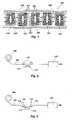
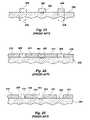
- FIG. 1illustrates a portion of an exemplary lead frame ribbon 100 .
- Individual lead frames 102each including a plurality of lead fingers 104 , are formed in a long, thin strip of conductive material 106 , such as copper, copper alloy, or the like.
- the lead frames 102are generally formed by a stamping process or an etching process.
- the lead frames 102are formed side-by-side along the conductive material strip 106 wherein the conductive material strip 106 includes a plurality of indexing holes 107 , 107 ′ on opposing lengthwise edges 109 , 109 ′, respectively, of the conductive material strip 106 .
- the indexing holes 107 , 107 ′are used to move the lead frame ribbon 100 and align the lead frames 102 throughout a process of attaching the lead frames 102 to semiconductor dice (not shown).
- FIGS. 2 and 3illustrate a schematic of one process of the present invention. Elements common to FIGS. 1 , 2 , and 3 retain the same numeric designation.
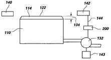
- the lead frame ribbon 100is fed from a source 108 , such as a spool, to an adhesive reservoir 110 .
- a source 108such as a spool
- the lead fingers 104 (not shown) of the lead frame 102 (not shown)are aligned over the adhesive reservoir 110 and the lead frame ribbon 100 is biased downward in direction 112 , such as by hydraulic, pneumatic, or electrically-powered biasing mechanisms 116 , to contact an adhesive material 114 .
- the adhesive material 114may be any viscous adhesive material including but not limited to thermoplastics, thermoses resins, flowable pastes, and B-stage adhesive materials.
- Preferred adhesive materials 114include cyanate ester, bismaleimide, epoxy, and polyimide.
- FIG. 4illustrates a schematic of another process of the present invention which is similar to the process of FIGS. 2 and 3 . Elements common to FIGS. 2 and 3 and FIG. 4 retain the same numeric designation. The only difference between the processes of FIGS. 2 and 3 and FIG. 4 is that the process of FIG. 4 employs an elevator mechanism 117 to move the adhesive reservoir 110 in an upward direction 120 to contact the lead fingers 104 (e.g., in FIG. 5 ) rather than biasing the lead frame ribbon 100 downward to the adhesive reservoir 110 .
- an elevator mechanism 117to move the adhesive reservoir 110 in an upward direction 120 to contact the lead fingers 104 (e.g., in FIG. 5 ) rather than biasing the lead frame ribbon 100 downward to the adhesive reservoir 110 .
- biasing and elevator mechanisms 116 and 117 shown in FIGS. 2 , 3 and 4are not required to bring the adhesive material 114 into contact with the lead fingers 104 .
- the lead fingers 104may be brought into close proximity to the adhesive reservoir 110 and additional adhesive material 114 may be delivered by a pump to the adhesive reservoir 110 to raise the level of the adhesive material 114 to contact the lead fingers 104 , or to provide a moving wave or surge of adhesive material traveling across the reservoir 110 .
- FIGS. 5–7illustrate side views of the lead fingers 104 being brought into contact with the adhesive material 114 and being retracted therefrom. Elements common to FIGS. 2–4 and FIGS. 5–7 retain the same numeric designation.
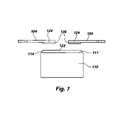
- the lead fingers 104are positioned over the adhesive reservoir 110 .
- the adhesive reservoir 110has the adhesive material 114 extending above edges 111 of the adhesive reservoir 110 . Due to the forces of adhesion and surface tension inherent in the adhesive material 114 , an exposed surface 122 of the adhesive material 114 will form a meniscus, or convex-shaped configuration, above the reservoir edges 111 .
- the lead fingers 104are lowered onto or proximate the exposed surface 122 of the adhesive material 114 .
- the adhesive material 114wets out across the bottom surface 124 of the lead fingers 104 .
- FIG. 7when the lead fingers 104 are retracted from the adhesive material 114 , the cohesion of the adhesive material 114 with the lead fingers 104 pulls some of the adhesive material 114 from the bulk of the adhesive material 114 to form an adhesive film 126 on the bottom surface 124 of the lead fingers 104 .
- the thickness of the adhesive film 126can range from 0.1 to 15 mils, depending on the viscosity of the adhesive material 114 .
- Changing the shape of the lead fingers 104 , changing the rheology of the adhesive material 114 , pre-coating the lead fingers 104 with a surfactant, such as AMP, or placing a solvent in the adhesive material 114 to improve wetting, and/or adding adhesion promoters, such as silane, siloxane, or polyimide siloxane, to the adhesive material 114will also change the thickness and/or pattern of the adhesive film 126 .
- the adhesive material 114must be capable of adhering to the lead fingers 104 and must not be of such a low viscosity that it drips when the lead fingers 104 are removed from contact with the exposed surface 122 of the adhesive material 114 .
- FIG. 8is a side cross-sectional view of a lead finger 104 after adhesive material 114 application.
- FIG. 9is a cross-sectional view of the lead finger 104 of FIG. 8 along line 9 — 9 .
- the adhesive material 114will not wet sides 128 of the lead finger 104 and, of course, will not collect on a bond wire surface 130 of a lead finger 104 (the bond wire surface 130 is the lead finger surface where a bond wire is subsequently attached during further processing). Since the adhesive material 114 does not collect on the bond wire surface 130 , there will be no adhesive material 114 to interfere with a subsequent wirebonding step subsequent to LOC attachment of the lead fingers 104 to an active surface of a semiconductor die.
- the adhesive reservoir 110can be shaped such that the exposed surface 122 of the adhesive material 114 is in a precise location.
- the adhesive material 114attaches to only specific, desired portions of the lead fingers 104 .
- the exposed surface 122be as level as possible. If the exposed surface 122 is not level, the lead fingers 104 may extend too deeply into the adhesive material 114 . When this occurs, the adhesive material 114 may wet the lead finger sides 128 and may even wet the lead finger bond wire surface 130 , as shown in FIG. 10 . If the adhesive material 114 wets the bond wire surface 130 , the adhesive material 114 may interfere with a wirebonding step subsequent to LOC attachment of the lead fingers 104 to an active surface of a semiconductor die, as mentioned above.
- exposed surface 122 of the adhesive material 114may be kept level. It is, of course, understood that exposed surface 122 extends from the adhesive reservoir 110 due to a slight excess of adhesive material 114 within the adhesive reservoir 110 .
- the adhesive material 114is pumped to the adhesive reservoir 110 from an adhesive material source (not shown) by a pump 132 .
- a desired exposed surface height 134 of exposed surface 122can be achieved by feeding an excess of adhesive material 114 into the adhesive reservoir 110 such that an initial exposed surface height 136 is higher than the desired exposed surface height 134 .
- a metering mechanism, such as wiper 138can be utilized to meter the adhesive material 114 from the initial exposed surface height 136 to the desired exposed surface height 134 .
- a desired exposed surface height 134 of exposed surface 122can be achieved by feeding an excess of adhesive material 114 into the adhesive reservoir 110 such that an initial exposed surface height 136 is higher than the desired exposed surface height 134 .
- the adhesive material 114is then drawn back (e.g., by vacuum 143 ), which results in a flattening of the exposed surface 122 .
- feed back and feed forward control schemesmay be used to control the desired exposed surface height 134 of the exposed surface 122 .
- One such control schemeis shown in FIG. 12 . Elements common to FIG. 11 and FIG. 12 retain the same numeric designations.
- a height detection mechanismshown as a light (preferably a laser) transmitter 140 and a light receiver 142 , is used to determine the height of the exposed surface 122 .
- the control signal 144 from control system 200triggers the pump 132 to stop or a valve (not shown) to shut when the desired exposed surface height 134 is achieved.
- a preferred method of controlling the levelness of the exposed surface 122is by forcing or extruding the adhesive material 114 through a coating stencil having small apertures, such as a screen or a plate with slots.
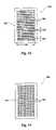
- a coating stencil 150is shown in FIG. 13 .
- the coating stencil 150is a flat plate 152 having a plurality of slots 154 .
- the coating stencil 150 shownhas twenty-three parallel slots 154 approximately 0.260 inch in length 158 and approximately 0.010 inch in width 160 , with the slots 154 being on parallel centerline pitch 162 of approximately 0.020 inch from one another.
- An alternate coating stencil 156is shown in FIG. 14 .
- the coating stencil 156is a screen comprising a flat plate 157 having a plurality of square or rectangular apertures 159 . It is, of course, understood that the apertures may be of any size (depending on the viscosity of the adhesive material) and any shape, including triangles, rectangles, squares, circles, ovals, or the like.
- the coating stencil 150is attached to an adhesive reservoir 180 .
- the exemplary adhesive reservoir 180shown in FIGS. 15 and 16 without the coating stencil 150 attached, comprises a housing 164 having an adhesive inflow chamber 166 in fluid communication with a pool chamber 168 .
- the coating stencil 150is attached proximate an upper surface 170 of the pool chamber 168 , such that the only upward outlet for the adhesive material is through the apertures in the coating stencil 150 .
- the adhesive reservoir 180may include an adhesive circulation mechanism to circulate the adhesive material to maintain the uniformity thereof.
- the cohesion between the aperture (slot) walls (not shown) and the adhesive material 114flattens out the exposed surface 122 of the adhesive material 114 .
- the cohesion between the aperture walls and the adhesive material 114basically pulls the adhesive material 114 down to the screen surface, which counteracts the force caused by the surface tension of the adhesive material 114 . As a result, the adhesive material 114 is pulled to the coating stencil 150 , thus flattening out.
- FIG. 17An example of the difference between a non-stenciled adhesive material exposed surface 172 and stenciled adhesive material exposed surface 174 is shown in FIG. 17 .
- the adhesive material 114was Ablestik XR-041395-9TM Polyimide LOC Adhesive (AblestikLaboratories, Collinso Dominguez, Calif.) and the coating stencil 150 was as described above for FIG. 13 .
- Ablestik XR-041395-9TMhas a viscosity of 62,000 cps at 25° C. and a thixotropic index of 3.5. It is, of course, understood that the width, length, pitch and shape of the apertures in the coating stencil 150 will vary for different viscosities of adhesive materials.
- a rule of thumb for determination of aperture sizeis that, for every viscosity increase of 25%, the aperture size should decrease by 50%.
- the illustration in FIG. 17is an AutoCadTM program rendering of a digitized measurement of the non-stenciled adhesive material exposed surface 172 and stenciled adhesive material exposed surface 174 .
- the maximum height 176 of the non-stenciled adhesive material exposed surface 172was approximately 0.07 inch above an upper surface 175 of the coating stencil 150 and the effective adhesion surface 178 of the non-stenciled adhesive material exposed surface 172 was approximately 0.26 inch wide.
- the maximum height 181 of the stenciled adhesive material exposed surface 174was approximately 0.05 inch and the effective adhesion surface 182 of the stenciled adhesive material exposed surface 174 was approximately 0.33 inch wide.
- the use of a coating stencil 150resulted in an increase of effective adhesion surface of about 21.2%.
- the effective adhesion surfaces 178 , 182are determined as the area from the maximum height 176 , 181 of the non-stenciled adhesive material exposed surface 172 and stenciled adhesive material exposed surface 174 , to a position about 5 mils below the maximum height 176 , 181 .
- FIG. 18illustrates such a profile using the same adhesive material 114 and coating stencil 150 described in FIG. 17 , wherein a vacuum 143 of between about 2 and 3 inches of H 2 O is applied.
- the vacuum 143 methodprovided a very uniform coating at between about 0.02 and 0.03 inch in adhesive material height.
- FIGS. 19–21An example of one preferred embodiment of the coating process is illustrated in FIGS. 19–21 . Elements common to FIGS. 19–21 and previous FIGS. retain the same designations.
- the lead fingers 104are brought into close proximity to the adhesive material exposed surface 122 .
- Sufficient adhesive material 114is then delivered to the adhesive reservoir 110 until the adhesive material exposed surface 122 comes in contact with the bottom surface 124 of the lead fingers 104 .
- additional adhesive material 114is delivered to the adhesive reservoir 110 to raise the adhesive material exposed surface 122 about an additional 0.02 to 0.06 inch so that the lead fingers 104 are submerged past a top surface 184 of the adhesive material exposed surface 122 , as shown in FIG. 20 .
- the lead fingers 104remain in this position for a time sufficient to allow the adhesive material 114 to wet the bottom surface 124 of the lead fingers 104 , preferably approximately 10 to 25 milliseconds. As shown in FIG. 21 , the adhesive material exposed surface 122 is then lowered, thereby forming the adhesive film 126 from the bulk of the adhesive material 114 on the bottom surface 124 of the lead fingers 104 . The lead frame ribbon 100 is then indexed to the next site that requires coating. Before the adhesive material 114 is raised again, more adhesive material 114 is delivered, as required, to replenish the amount used in the previous coating cycle.
- multiple reservoirs 110could be configured as shown in FIG. 22 .
- the adhesive material 114can be applied to the lead fingers 104 of multiple lead frames 102 simultaneously.
- the lead frame ribbon 100may, optionally, be fed to a curing oven 118 , shown in FIGS. 2 , 3 , 4 , and 22 , to set the adhesive material 114 .
- a semiconductor die(not shown) then can be attached to a lead frame 102 and adhesive film 126 by known LOC attach methods.
Landscapes
- Engineering & Computer Science (AREA)
- Computer Hardware Design (AREA)
- Microelectronics & Electronic Packaging (AREA)
- Power Engineering (AREA)
- Manufacturing & Machinery (AREA)
- Physics & Mathematics (AREA)
- Condensed Matter Physics & Semiconductors (AREA)
- General Physics & Mathematics (AREA)
- Die Bonding (AREA)
- Application Of Or Painting With Fluid Materials (AREA)
- Coating Apparatus (AREA)
Abstract
Description
Claims (163)
Priority Applications (1)
| Application Number | Priority Date | Filing Date | Title |
|---|---|---|---|
| US10/361,240US7087116B2 (en) | 1997-08-05 | 2003-02-10 | Apparatus for modifying the configuration of an exposed surface of a viscous fluid |
Applications Claiming Priority (3)
| Application Number | Priority Date | Filing Date | Title |
|---|---|---|---|
| US08/906,578US6336973B1 (en) | 1997-08-05 | 1997-08-05 | Apparatus and method for modifying the configuration of an exposed surface of a viscous fluid |
| US09/944,233US6890384B2 (en) | 1997-08-05 | 2001-08-30 | Apparatus and method for modifying the configuration of an exposed surface of a viscous fluid |
| US10/361,240US7087116B2 (en) | 1997-08-05 | 2003-02-10 | Apparatus for modifying the configuration of an exposed surface of a viscous fluid |
Related Parent Applications (1)
| Application Number | Title | Priority Date | Filing Date |
|---|---|---|---|
| US09/944,233ContinuationUS6890384B2 (en) | 1997-08-05 | 2001-08-30 | Apparatus and method for modifying the configuration of an exposed surface of a viscous fluid |
Publications (2)
| Publication Number | Publication Date |
|---|---|
| US20030116085A1 US20030116085A1 (en) | 2003-06-26 |
| US7087116B2true US7087116B2 (en) | 2006-08-08 |
Family
ID=25422671
Family Applications (4)
| Application Number | Title | Priority Date | Filing Date |
|---|---|---|---|
| US08/906,578Expired - Fee RelatedUS6336973B1 (en) | 1997-08-05 | 1997-08-05 | Apparatus and method for modifying the configuration of an exposed surface of a viscous fluid |
| US09/531,551Expired - Fee RelatedUS6485778B1 (en) | 1997-08-05 | 2000-03-20 | Method of applying an adhesive material to lead fingers of a lead frame |
| US09/944,233Expired - LifetimeUS6890384B2 (en) | 1997-08-05 | 2001-08-30 | Apparatus and method for modifying the configuration of an exposed surface of a viscous fluid |
| US10/361,240Expired - Fee RelatedUS7087116B2 (en) | 1997-08-05 | 2003-02-10 | Apparatus for modifying the configuration of an exposed surface of a viscous fluid |
Family Applications Before (3)
| Application Number | Title | Priority Date | Filing Date |
|---|---|---|---|
| US08/906,578Expired - Fee RelatedUS6336973B1 (en) | 1997-08-05 | 1997-08-05 | Apparatus and method for modifying the configuration of an exposed surface of a viscous fluid |
| US09/531,551Expired - Fee RelatedUS6485778B1 (en) | 1997-08-05 | 2000-03-20 | Method of applying an adhesive material to lead fingers of a lead frame |
| US09/944,233Expired - LifetimeUS6890384B2 (en) | 1997-08-05 | 2001-08-30 | Apparatus and method for modifying the configuration of an exposed surface of a viscous fluid |
Country Status (1)
| Country | Link |
|---|---|
| US (4) | US6336973B1 (en) |
Families Citing this family (4)
| Publication number | Priority date | Publication date | Assignee | Title |
|---|---|---|---|---|
| US7174626B2 (en)* | 1999-06-30 | 2007-02-13 | Intersil Americas, Inc. | Method of manufacturing a plated electronic termination |
| US6638831B1 (en) | 2000-08-31 | 2003-10-28 | Micron Technology, Inc. | Use of a reference fiducial on a semiconductor package to monitor and control a singulation method |
| JP4005077B2 (en)* | 2004-11-22 | 2007-11-07 | Necエレクトロニクス株式会社 | Manufacturing method of semiconductor device and coating method of viscous liquid |
| DE102007039949B3 (en)* | 2007-08-23 | 2008-12-04 | Flooring Technologies Ltd. | Device for applying a suspension to a carrier plate |
Citations (63)
| Publication number | Priority date | Publication date | Assignee | Title |
|---|---|---|---|---|
| US2506047A (en) | 1946-12-31 | 1950-05-02 | Sylvania Electric Prod | Protective device for use in soldering operations |
| US2964007A (en) | 1956-02-16 | 1960-12-13 | Gen Mills Inc | Dip soldering machine |
| US3713876A (en) | 1970-04-07 | 1973-01-30 | Western Electric Co | Methods of metal coating articles |
| US3828419A (en) | 1971-09-29 | 1974-08-13 | Zevatron Gmbh | Automatic soldering machine |
| US3999479A (en) | 1974-04-30 | 1976-12-28 | Peter Zimmer | Dyestuff applicator |
| US4045863A (en) | 1971-06-03 | 1977-09-06 | Siemens Aktiengesellschaft | Method of producing metallic carrier system for a multi-electrode semiconductor strip |
| US4300153A (en) | 1977-09-22 | 1981-11-10 | Sharp Kabushiki Kaisha | Flat shaped semiconductor encapsulation |
| US4346124A (en) | 1981-05-04 | 1982-08-24 | Laurier Associates, Inc. | Method of applying an adhesive to a circuit chip |
| US4355463A (en) | 1980-03-24 | 1982-10-26 | National Semiconductor Corporation | Process for hermetically encapsulating semiconductor devices |
| US4360144A (en) | 1981-01-21 | 1982-11-23 | Basf Wyandotte Corporation | Printed circuit board soldering |
| US4526740A (en) | 1982-05-13 | 1985-07-02 | Motorola, Inc. | Method of forming a ring of viscous material against a substrate |
| US4687693A (en) | 1985-06-13 | 1987-08-18 | Stauffer Chemical Company | Adhesively mountable die attach film |
| US4690999A (en) | 1983-08-01 | 1987-09-01 | Hitachi, Ltd. | Low thermal expansion resin material and composite shaped article |
| US4862245A (en) | 1985-04-18 | 1989-08-29 | International Business Machines Corporation | Package semiconductor chip |
| US4876221A (en) | 1988-05-03 | 1989-10-24 | Matsushita Electric Industrial Co., Ltd. | Bonding method |
| JPH0237964A (en) | 1988-07-27 | 1990-02-07 | Mitsubishi Electric Corp | Automatic solder level adjustment device |
| US4932585A (en) | 1989-04-20 | 1990-06-12 | Senju Metal Industry Co., Ltd. | Method and apparatus for solder plating an object |
| US4942140A (en) | 1987-03-25 | 1990-07-17 | Mitsubishi Denki Kabushiki Kaisha | Method of packaging semiconductor device |
| US4959008A (en) | 1984-04-30 | 1990-09-25 | National Starch And Chemical Investment Holding Corporation | Pre-patterned circuit board device-attach adhesive transfer system |
| US5030308A (en) | 1986-07-14 | 1991-07-09 | National Starch And Chemical Investment Holding Corporation | Method of bonding a semiconductor chip to a substrate |
| US5049434A (en) | 1984-04-30 | 1991-09-17 | National Starch And Chemical Investment Holding Corporation | Pre-patterned device substrate device-attach adhesive transfer system |
| US5066614A (en) | 1988-11-21 | 1991-11-19 | Honeywell Inc. | Method of manufacturing a leadframe having conductive elements preformed with solder bumps |
| US5105661A (en) | 1989-12-28 | 1992-04-21 | Kureha Chemical Industry Company, Limited | Method of detecting a level of liquid in a moving cylindrical body |
| US5140404A (en) | 1990-10-24 | 1992-08-18 | Micron Technology, Inc. | Semiconductor device manufactured by a method for attaching a semiconductor die to a leadframe using a thermoplastic covered carrier tape |
| US5139973A (en) | 1990-12-17 | 1992-08-18 | Allegro Microsystems, Inc. | Method for making a semiconductor package with the distance between a lead frame die pad and heat spreader determined by the thickness of an intermediary insulating sheet |
| US5164010A (en) | 1990-10-02 | 1992-11-17 | Seiko Epson Corporation | Solder coating method and apparatus for semiconductor devices |
| US5183508A (en) | 1987-11-23 | 1993-02-02 | Epicor Technology, Inc. | Apparatus for patch coating printed circuit boards |
| US5185040A (en) | 1988-12-19 | 1993-02-09 | Murata Manufacturing Co., Ltd. | Apparatus for forming electrode on electronic component |
| US5256598A (en) | 1992-04-15 | 1993-10-26 | Micron Technology, Inc. | Shrink accommodating lead frame |
| US5275661A (en) | 1991-11-08 | 1994-01-04 | Murata Mfg. Co., Ltd. | Dipping apparatus |
| US5286679A (en) | 1993-03-18 | 1994-02-15 | Micron Technology, Inc. | Method for attaching a semiconductor die to a leadframe using a patterned adhesive layer |
| US5302849A (en) | 1993-03-01 | 1994-04-12 | Motorola, Inc. | Plastic and grid array semiconductor device and method for making the same |
| US5304842A (en) | 1990-10-24 | 1994-04-19 | Micron Technology, Inc. | Dissimilar adhesive die attach for semiconductor devices |
| US5322207A (en) | 1993-05-03 | 1994-06-21 | Micron Semiconductor Inc. | Method and apparatus for wire bonding semiconductor dice to a leadframe |
| US5388752A (en) | 1993-04-23 | 1995-02-14 | Kawakatsu; Ichiro | Method and apparatus for soldering a workpiece in a non-oxidizing gas atmosphere |
| US5409863A (en) | 1993-02-19 | 1995-04-25 | Lsi Logic Corporation | Method and apparatus for controlling adhesive spreading when attaching an integrated circuit die |
| USRE35027E (en) | 1988-09-22 | 1995-08-29 | Delaware Capital Formation, Inc. | Pick and place method and apparatus |
| US5482736A (en) | 1994-08-04 | 1996-01-09 | Amkor Electronics, Inc. | Method for applying flux to ball grid array package |
| US5548160A (en) | 1994-11-14 | 1996-08-20 | Micron Technology, Inc. | Method and structure for attaching a semiconductor die to a lead frame |
| US5559046A (en) | 1992-10-28 | 1996-09-24 | Matsushita Electronics Corporation | Semiconductor device having a hollow around a gate electrode and a method for producing the same |
| US5563443A (en) | 1993-03-13 | 1996-10-08 | Texas Instruments Incorporated | Packaged semiconductor device utilizing leadframe attached on a semiconductor chip |
| US5585282A (en) | 1991-06-04 | 1996-12-17 | Micron Technology, Inc. | Process for forming a raised portion on a projecting contact for electrical testing of a semiconductor |
| US5617990A (en) | 1995-07-03 | 1997-04-08 | Micron Electronics, Inc. | Shield and method for selective wave soldering |
| US5696033A (en) | 1995-08-16 | 1997-12-09 | Micron Technology, Inc. | Method for packaging a semiconductor die |
| US5725143A (en) | 1996-05-07 | 1998-03-10 | L'air Liquide, Societe Anonyme Pour L'etude Et L'exploitation Des Procedes Georges Claude | Method and machine for wave soldering or tinning |
| US5733800A (en) | 1996-05-21 | 1998-03-31 | Micron Technology, Inc. | Underfill coating for LOC package |
| US5739053A (en) | 1992-10-27 | 1998-04-14 | Matsushita Electric Industrial Co., Ltd. | Process for bonding a semiconductor to a circuit substrate including a solder bump transferring step |
| US5747102A (en) | 1995-11-16 | 1998-05-05 | Nordson Corporation | Method and apparatus for dispensing small amounts of liquid material |
| US5769947A (en) | 1994-10-22 | 1998-06-23 | Itw Dynatech Gmbh Klebetechnik | Applicator for adhesive and corresponding nozzle plate |
| US5773322A (en) | 1995-05-01 | 1998-06-30 | Lucent Technologies Inc. | Molded encapsulated electronic component |
| US5810926A (en) | 1996-03-11 | 1998-09-22 | Micron Technology, Inc. | Method and apparatus for applying atomized adhesive to a leadframe for chip bonding |
| US5834062A (en) | 1996-06-27 | 1998-11-10 | Motorola, Inc. | Material transfer apparatus and method of using the same |
| US5877542A (en) | 1996-05-16 | 1999-03-02 | Oki Electric Industry Co., Ltd. | Plastic molded type semiconductor device |
| US5885854A (en) | 1996-11-12 | 1999-03-23 | Micron Technology, Inc. | Method for application of de-wetting material for glob top applications |
| US5901899A (en) | 1995-09-26 | 1999-05-11 | U.S. Philips Corporation | Wave soldering machine and method of adjusting and automatically controlling the height of a solder wave |
| US5907246A (en) | 1995-11-29 | 1999-05-25 | Lucent Technologies, Inc. | Testing of semiconductor chips |
| US5923957A (en) | 1996-05-10 | 1999-07-13 | Samsung Electronics Co., Ltd. | Process for manufacturing a lead-on-chip semiconductor device package having a discontinuous adhesive layer formed from liquid adhesive |
| US5959347A (en) | 1997-08-14 | 1999-09-28 | Micron Technology, Inc. | LOC semiconductor assembled with room temperature adhesive |
| US6010570A (en) | 1996-08-30 | 2000-01-04 | Tokyo Electron Limited | Apparatus for forming coating film for semiconductor processing |
| US6040205A (en) | 1997-08-05 | 2000-03-21 | Micron Technology, Inc. | Apparatus and method for controlling the depth of immersion of a semiconductor element in an exposed surface of a viscous fluid |
| US6083768A (en) | 1996-09-06 | 2000-07-04 | Micron Technology, Inc. | Gravitationally-assisted control of spread of viscous material applied to semiconductor assembly components |
| US6133068A (en) | 1997-10-06 | 2000-10-17 | Micron Technology, Inc. | Increasing the gap between a lead frame and a semiconductor die |
| US6204093B1 (en) | 1997-08-21 | 2001-03-20 | Micron Technology, Inc. | Method and apparatus for applying viscous materials to a lead frame |
- 1997
- 1997-08-05USUS08/906,578patent/US6336973B1/ennot_activeExpired - Fee Related
- 2000
- 2000-03-20USUS09/531,551patent/US6485778B1/ennot_activeExpired - Fee Related
- 2001
- 2001-08-30USUS09/944,233patent/US6890384B2/ennot_activeExpired - Lifetime
- 2003
- 2003-02-10USUS10/361,240patent/US7087116B2/ennot_activeExpired - Fee Related
Patent Citations (63)
| Publication number | Priority date | Publication date | Assignee | Title |
|---|---|---|---|---|
| US2506047A (en) | 1946-12-31 | 1950-05-02 | Sylvania Electric Prod | Protective device for use in soldering operations |
| US2964007A (en) | 1956-02-16 | 1960-12-13 | Gen Mills Inc | Dip soldering machine |
| US3713876A (en) | 1970-04-07 | 1973-01-30 | Western Electric Co | Methods of metal coating articles |
| US4045863A (en) | 1971-06-03 | 1977-09-06 | Siemens Aktiengesellschaft | Method of producing metallic carrier system for a multi-electrode semiconductor strip |
| US3828419A (en) | 1971-09-29 | 1974-08-13 | Zevatron Gmbh | Automatic soldering machine |
| US3999479A (en) | 1974-04-30 | 1976-12-28 | Peter Zimmer | Dyestuff applicator |
| US4300153A (en) | 1977-09-22 | 1981-11-10 | Sharp Kabushiki Kaisha | Flat shaped semiconductor encapsulation |
| US4355463A (en) | 1980-03-24 | 1982-10-26 | National Semiconductor Corporation | Process for hermetically encapsulating semiconductor devices |
| US4360144A (en) | 1981-01-21 | 1982-11-23 | Basf Wyandotte Corporation | Printed circuit board soldering |
| US4346124A (en) | 1981-05-04 | 1982-08-24 | Laurier Associates, Inc. | Method of applying an adhesive to a circuit chip |
| US4526740A (en) | 1982-05-13 | 1985-07-02 | Motorola, Inc. | Method of forming a ring of viscous material against a substrate |
| US4690999A (en) | 1983-08-01 | 1987-09-01 | Hitachi, Ltd. | Low thermal expansion resin material and composite shaped article |
| US4959008A (en) | 1984-04-30 | 1990-09-25 | National Starch And Chemical Investment Holding Corporation | Pre-patterned circuit board device-attach adhesive transfer system |
| US5049434A (en) | 1984-04-30 | 1991-09-17 | National Starch And Chemical Investment Holding Corporation | Pre-patterned device substrate device-attach adhesive transfer system |
| US4862245A (en) | 1985-04-18 | 1989-08-29 | International Business Machines Corporation | Package semiconductor chip |
| US4687693A (en) | 1985-06-13 | 1987-08-18 | Stauffer Chemical Company | Adhesively mountable die attach film |
| US5030308A (en) | 1986-07-14 | 1991-07-09 | National Starch And Chemical Investment Holding Corporation | Method of bonding a semiconductor chip to a substrate |
| US4942140A (en) | 1987-03-25 | 1990-07-17 | Mitsubishi Denki Kabushiki Kaisha | Method of packaging semiconductor device |
| US5183508A (en) | 1987-11-23 | 1993-02-02 | Epicor Technology, Inc. | Apparatus for patch coating printed circuit boards |
| US4876221A (en) | 1988-05-03 | 1989-10-24 | Matsushita Electric Industrial Co., Ltd. | Bonding method |
| JPH0237964A (en) | 1988-07-27 | 1990-02-07 | Mitsubishi Electric Corp | Automatic solder level adjustment device |
| USRE35027E (en) | 1988-09-22 | 1995-08-29 | Delaware Capital Formation, Inc. | Pick and place method and apparatus |
| US5066614A (en) | 1988-11-21 | 1991-11-19 | Honeywell Inc. | Method of manufacturing a leadframe having conductive elements preformed with solder bumps |
| US5185040A (en) | 1988-12-19 | 1993-02-09 | Murata Manufacturing Co., Ltd. | Apparatus for forming electrode on electronic component |
| US4932585A (en) | 1989-04-20 | 1990-06-12 | Senju Metal Industry Co., Ltd. | Method and apparatus for solder plating an object |
| US5105661A (en) | 1989-12-28 | 1992-04-21 | Kureha Chemical Industry Company, Limited | Method of detecting a level of liquid in a moving cylindrical body |
| US5164010A (en) | 1990-10-02 | 1992-11-17 | Seiko Epson Corporation | Solder coating method and apparatus for semiconductor devices |
| US5140404A (en) | 1990-10-24 | 1992-08-18 | Micron Technology, Inc. | Semiconductor device manufactured by a method for attaching a semiconductor die to a leadframe using a thermoplastic covered carrier tape |
| US5304842A (en) | 1990-10-24 | 1994-04-19 | Micron Technology, Inc. | Dissimilar adhesive die attach for semiconductor devices |
| US5139973A (en) | 1990-12-17 | 1992-08-18 | Allegro Microsystems, Inc. | Method for making a semiconductor package with the distance between a lead frame die pad and heat spreader determined by the thickness of an intermediary insulating sheet |
| US5585282A (en) | 1991-06-04 | 1996-12-17 | Micron Technology, Inc. | Process for forming a raised portion on a projecting contact for electrical testing of a semiconductor |
| US5275661A (en) | 1991-11-08 | 1994-01-04 | Murata Mfg. Co., Ltd. | Dipping apparatus |
| US5256598A (en) | 1992-04-15 | 1993-10-26 | Micron Technology, Inc. | Shrink accommodating lead frame |
| US5739053A (en) | 1992-10-27 | 1998-04-14 | Matsushita Electric Industrial Co., Ltd. | Process for bonding a semiconductor to a circuit substrate including a solder bump transferring step |
| US5559046A (en) | 1992-10-28 | 1996-09-24 | Matsushita Electronics Corporation | Semiconductor device having a hollow around a gate electrode and a method for producing the same |
| US5409863A (en) | 1993-02-19 | 1995-04-25 | Lsi Logic Corporation | Method and apparatus for controlling adhesive spreading when attaching an integrated circuit die |
| US5302849A (en) | 1993-03-01 | 1994-04-12 | Motorola, Inc. | Plastic and grid array semiconductor device and method for making the same |
| US5563443A (en) | 1993-03-13 | 1996-10-08 | Texas Instruments Incorporated | Packaged semiconductor device utilizing leadframe attached on a semiconductor chip |
| US5286679A (en) | 1993-03-18 | 1994-02-15 | Micron Technology, Inc. | Method for attaching a semiconductor die to a leadframe using a patterned adhesive layer |
| US5388752A (en) | 1993-04-23 | 1995-02-14 | Kawakatsu; Ichiro | Method and apparatus for soldering a workpiece in a non-oxidizing gas atmosphere |
| US5322207A (en) | 1993-05-03 | 1994-06-21 | Micron Semiconductor Inc. | Method and apparatus for wire bonding semiconductor dice to a leadframe |
| US5482736A (en) | 1994-08-04 | 1996-01-09 | Amkor Electronics, Inc. | Method for applying flux to ball grid array package |
| US5769947A (en) | 1994-10-22 | 1998-06-23 | Itw Dynatech Gmbh Klebetechnik | Applicator for adhesive and corresponding nozzle plate |
| US5548160A (en) | 1994-11-14 | 1996-08-20 | Micron Technology, Inc. | Method and structure for attaching a semiconductor die to a lead frame |
| US5773322A (en) | 1995-05-01 | 1998-06-30 | Lucent Technologies Inc. | Molded encapsulated electronic component |
| US5617990A (en) | 1995-07-03 | 1997-04-08 | Micron Electronics, Inc. | Shield and method for selective wave soldering |
| US5696033A (en) | 1995-08-16 | 1997-12-09 | Micron Technology, Inc. | Method for packaging a semiconductor die |
| US5901899A (en) | 1995-09-26 | 1999-05-11 | U.S. Philips Corporation | Wave soldering machine and method of adjusting and automatically controlling the height of a solder wave |
| US5747102A (en) | 1995-11-16 | 1998-05-05 | Nordson Corporation | Method and apparatus for dispensing small amounts of liquid material |
| US5907246A (en) | 1995-11-29 | 1999-05-25 | Lucent Technologies, Inc. | Testing of semiconductor chips |
| US5810926A (en) | 1996-03-11 | 1998-09-22 | Micron Technology, Inc. | Method and apparatus for applying atomized adhesive to a leadframe for chip bonding |
| US5725143A (en) | 1996-05-07 | 1998-03-10 | L'air Liquide, Societe Anonyme Pour L'etude Et L'exploitation Des Procedes Georges Claude | Method and machine for wave soldering or tinning |
| US5923957A (en) | 1996-05-10 | 1999-07-13 | Samsung Electronics Co., Ltd. | Process for manufacturing a lead-on-chip semiconductor device package having a discontinuous adhesive layer formed from liquid adhesive |
| US5877542A (en) | 1996-05-16 | 1999-03-02 | Oki Electric Industry Co., Ltd. | Plastic molded type semiconductor device |
| US5733800A (en) | 1996-05-21 | 1998-03-31 | Micron Technology, Inc. | Underfill coating for LOC package |
| US5834062A (en) | 1996-06-27 | 1998-11-10 | Motorola, Inc. | Material transfer apparatus and method of using the same |
| US6010570A (en) | 1996-08-30 | 2000-01-04 | Tokyo Electron Limited | Apparatus for forming coating film for semiconductor processing |
| US6083768A (en) | 1996-09-06 | 2000-07-04 | Micron Technology, Inc. | Gravitationally-assisted control of spread of viscous material applied to semiconductor assembly components |
| US5885854A (en) | 1996-11-12 | 1999-03-23 | Micron Technology, Inc. | Method for application of de-wetting material for glob top applications |
| US6040205A (en) | 1997-08-05 | 2000-03-21 | Micron Technology, Inc. | Apparatus and method for controlling the depth of immersion of a semiconductor element in an exposed surface of a viscous fluid |
| US5959347A (en) | 1997-08-14 | 1999-09-28 | Micron Technology, Inc. | LOC semiconductor assembled with room temperature adhesive |
| US6204093B1 (en) | 1997-08-21 | 2001-03-20 | Micron Technology, Inc. | Method and apparatus for applying viscous materials to a lead frame |
| US6133068A (en) | 1997-10-06 | 2000-10-17 | Micron Technology, Inc. | Increasing the gap between a lead frame and a semiconductor die |
Also Published As
| Publication number | Publication date |
|---|---|
| US20030116085A1 (en) | 2003-06-26 |
| US6890384B2 (en) | 2005-05-10 |
| US6485778B1 (en) | 2002-11-26 |
| US6336973B1 (en) | 2002-01-08 |
| US20020029742A1 (en) | 2002-03-14 |
Similar Documents
| Publication | Publication Date | Title |
|---|---|---|
| US6436732B2 (en) | Apparatus for applying viscous materials to a lead frame | |
| US6346152B1 (en) | Method and apparatus for applying adhesives to a lead frame | |
| US5286679A (en) | Method for attaching a semiconductor die to a leadframe using a patterned adhesive layer | |
| US6368897B1 (en) | Method for manufactoring and using stencil/screen | |
| US6528867B1 (en) | Integrated circuit devices including connection components mechanically and electrically attached to semiconductor dice | |
| US6083819A (en) | Method and assembly for providing improved underchip encapsulation | |
| US6919229B2 (en) | Method for controlling the depth of immersion of a semiconductor element in an exposed surface of a viscous fluid | |
| US6793749B2 (en) | Automated method of attaching flip-chip devices to a substrate | |
| TW200935532A (en) | Dispensing solder for mounting semiconductor chips | |
| CN111819686A (en) | Self-alignment between circuit die and interconnect | |
| US7087116B2 (en) | Apparatus for modifying the configuration of an exposed surface of a viscous fluid | |
| US20020001879A1 (en) | Gravitationally-assisted control of spread of viscous material applied to semiconductor assembly components | |
| US6143076A (en) | Applicator head | |
| EP1459808A2 (en) | Method of implementing multiple pump speeds for dispensing a viscous material | |
| US20020182774A1 (en) | Die-attach method and assemblies using film and epoxy bonds | |
| US6246106B1 (en) | Lead frame | |
| CN1101597C (en) | Lead-on-chip type semiconductor chip package using adhesive deposited on chip active surfaces in wafer level and method for manufacturing the same | |
| US7735717B2 (en) | Method of manufacturing semiconductor apparatus and method of forming viscous liquid layer | |
| KR100197858B1 (en) | Improved chip attaching method to the lead frame using screen printing technique | |
| JPH11219987A (en) | Tab semiconductor device and manufacture thereof |
Legal Events
| Date | Code | Title | Description |
|---|---|---|---|
| FEPP | Fee payment procedure | Free format text:PAYOR NUMBER ASSIGNED (ORIGINAL EVENT CODE: ASPN); ENTITY STATUS OF PATENT OWNER: LARGE ENTITY | |
| CC | Certificate of correction | ||
| FPAY | Fee payment | Year of fee payment:4 | |
| FPAY | Fee payment | Year of fee payment:8 | |
| AS | Assignment | Owner name:U.S. BANK NATIONAL ASSOCIATION, AS COLLATERAL AGENT, CALIFORNIA Free format text:SECURITY INTEREST;ASSIGNOR:MICRON TECHNOLOGY, INC.;REEL/FRAME:038669/0001 Effective date:20160426 Owner name:U.S. BANK NATIONAL ASSOCIATION, AS COLLATERAL AGEN Free format text:SECURITY INTEREST;ASSIGNOR:MICRON TECHNOLOGY, INC.;REEL/FRAME:038669/0001 Effective date:20160426 | |
| AS | Assignment | Owner name:MORGAN STANLEY SENIOR FUNDING, INC., AS COLLATERAL AGENT, MARYLAND Free format text:PATENT SECURITY AGREEMENT;ASSIGNOR:MICRON TECHNOLOGY, INC.;REEL/FRAME:038954/0001 Effective date:20160426 Owner name:MORGAN STANLEY SENIOR FUNDING, INC., AS COLLATERAL Free format text:PATENT SECURITY AGREEMENT;ASSIGNOR:MICRON TECHNOLOGY, INC.;REEL/FRAME:038954/0001 Effective date:20160426 | |
| AS | Assignment | Owner name:U.S. BANK NATIONAL ASSOCIATION, AS COLLATERAL AGENT, CALIFORNIA Free format text:CORRECTIVE ASSIGNMENT TO CORRECT THE REPLACE ERRONEOUSLY FILED PATENT #7358718 WITH THE CORRECT PATENT #7358178 PREVIOUSLY RECORDED ON REEL 038669 FRAME 0001. ASSIGNOR(S) HEREBY CONFIRMS THE SECURITY INTEREST;ASSIGNOR:MICRON TECHNOLOGY, INC.;REEL/FRAME:043079/0001 Effective date:20160426 Owner name:U.S. BANK NATIONAL ASSOCIATION, AS COLLATERAL AGEN Free format text:CORRECTIVE ASSIGNMENT TO CORRECT THE REPLACE ERRONEOUSLY FILED PATENT #7358718 WITH THE CORRECT PATENT #7358178 PREVIOUSLY RECORDED ON REEL 038669 FRAME 0001. ASSIGNOR(S) HEREBY CONFIRMS THE SECURITY INTEREST;ASSIGNOR:MICRON TECHNOLOGY, INC.;REEL/FRAME:043079/0001 Effective date:20160426 | |
| FEPP | Fee payment procedure | Free format text:MAINTENANCE FEE REMINDER MAILED (ORIGINAL EVENT CODE: REM.) | |
| AS | Assignment | Owner name:MICRON TECHNOLOGY, INC., IDAHO Free format text:RELEASE BY SECURED PARTY;ASSIGNOR:U.S. BANK NATIONAL ASSOCIATION, AS COLLATERAL AGENT;REEL/FRAME:047243/0001 Effective date:20180629 | |
| LAPS | Lapse for failure to pay maintenance fees | Free format text:PATENT EXPIRED FOR FAILURE TO PAY MAINTENANCE FEES (ORIGINAL EVENT CODE: EXP.); ENTITY STATUS OF PATENT OWNER: LARGE ENTITY | |
| STCH | Information on status: patent discontinuation | Free format text:PATENT EXPIRED DUE TO NONPAYMENT OF MAINTENANCE FEES UNDER 37 CFR 1.362 | |
| FP | Lapsed due to failure to pay maintenance fee | Effective date:20180808 | |
| AS | Assignment | Owner name:MICRON TECHNOLOGY, INC., IDAHO Free format text:RELEASE BY SECURED PARTY;ASSIGNOR:MORGAN STANLEY SENIOR FUNDING, INC., AS COLLATERAL AGENT;REEL/FRAME:050937/0001 Effective date:20190731 |