US7084720B2 - Printed bandpass filter for a double conversion tuner - Google Patents
Printed bandpass filter for a double conversion tunerDownload PDFInfo
- Publication number
- US7084720B2 US7084720B2US10/040,376US4037602AUS7084720B2US 7084720 B2US7084720 B2US 7084720B2US 4037602 AUS4037602 AUS 4037602AUS 7084720 B2US7084720 B2US 7084720B2
- Authority
- US
- United States
- Prior art keywords
- bypass line
- coupled
- output
- input
- spiral resonator
- Prior art date
- Legal status (The legal status is an assumption and is not a legal conclusion. Google has not performed a legal analysis and makes no representation as to the accuracy of the status listed.)
- Expired - Fee Related
Links
Images


Classifications
- H—ELECTRICITY
- H01—ELECTRIC ELEMENTS
- H01P—WAVEGUIDES; RESONATORS, LINES, OR OTHER DEVICES OF THE WAVEGUIDE TYPE
- H01P7/00—Resonators of the waveguide type
- H—ELECTRICITY
- H01—ELECTRIC ELEMENTS
- H01P—WAVEGUIDES; RESONATORS, LINES, OR OTHER DEVICES OF THE WAVEGUIDE TYPE
- H01P1/00—Auxiliary devices
- H01P1/20—Frequency-selective devices, e.g. filters
- H01P1/201—Filters for transverse electromagnetic waves
- H01P1/203—Strip line filters
- H—ELECTRICITY
- H01—ELECTRIC ELEMENTS
- H01P—WAVEGUIDES; RESONATORS, LINES, OR OTHER DEVICES OF THE WAVEGUIDE TYPE
- H01P1/00—Auxiliary devices
- H01P1/20—Frequency-selective devices, e.g. filters
- H—ELECTRICITY
- H01—ELECTRIC ELEMENTS
- H01P—WAVEGUIDES; RESONATORS, LINES, OR OTHER DEVICES OF THE WAVEGUIDE TYPE
- H01P1/00—Auxiliary devices
- H01P1/20—Frequency-selective devices, e.g. filters
- H01P1/201—Filters for transverse electromagnetic waves
- H01P1/203—Strip line filters
- H01P1/20327—Electromagnetic interstage coupling
- H01P1/20354—Non-comb or non-interdigital filters
- H01P1/20381—Special shape resonators
- H—ELECTRICITY
- H05—ELECTRIC TECHNIQUES NOT OTHERWISE PROVIDED FOR
- H05K—PRINTED CIRCUITS; CASINGS OR CONSTRUCTIONAL DETAILS OF ELECTRIC APPARATUS; MANUFACTURE OF ASSEMBLAGES OF ELECTRICAL COMPONENTS
- H05K1/00—Printed circuits
- H05K1/16—Printed circuits incorporating printed electric components, e.g. printed resistor, capacitor, inductor
- H05K1/165—Printed circuits incorporating printed electric components, e.g. printed resistor, capacitor, inductor incorporating printed inductors
Definitions
- the present inventionrelates generally to radio frequency signal filters, and more specifically to printed circuit bandpass filters.
- Television tunerscan be classified by the type of circuit used to select the desired television channel.
- the predominant circuit architectures in use todayare single-conversion and double-conversion television tuners.
- Single conversion tunersusually require preselection filtering.
- the preselectormust be a tracking bandpass filter in order to reject the image channel, which occurs at twice the intermediate frequency (IF) away from the desired television channel frequency.
- Tracking filtersrequire expensive manual tuning during the assembly process. Tracking filters can have significant variations in amplitude response over the desired television channel bandwidth. These variations are undesirable in both analog and digital television systems. Tracking filters are also particularly difficult to implement at the upper end of the television band, where the difference between the desired television channel frequency and the image frequency is a small fraction of the desired television frequency. Removing the image channel, under these conditions, requires a bandpass filter with high selectivity.
- Double-conversion tunersconvert the incoming television signal to a high IF, where most of the out-of-band signals are removed by a narrow bandpass filter.
- This high IF bandpass filteris usually implemented as either a surface acoustic wave (SAW) filter or a manually-tuned LC filter.
- SAWsurface acoustic wave
- the high IF bandpass filterpasses a few channels, out of more than 100 channels in the television band.
- a second conversionbrings this relatively narrowband signal composed of a few channels down to the standard television IF at about 40 MHz.
- a second SAW or LC filtereliminates the remaining undesired channels.
- a tracking filteris not required for image rejection. It is easier to obtain a high level of image rejection with the double-conversion approach, because a fixed surface acoustic wave and a fixed LC filter can be much more selective than a tracking LC filter.
- the high IF bandpass filterwhich is usually centered a few hundred megahertz above the upper limit of the television band, must be wide enough to pass the desired television channel under all conditions of center-frequency manufacturing tolerance; center-frequency temperature and other environmental drift; and the variability of the high IF center frequency due to coarseness in tuning the first local oscillator.
- a fixed LC filteris composed of lumped element capacitors and inductors. Variations in the values of these components and variations in the characteristics of the underlying substrate cause a shift in the filter's characteristics, center frequency, bandwidth, etc., during fabrication. To compensate, lumped element filters must be tuned after fabrication. Tuning raises the cost and complexity of the filter assembly process.
- SAW filtersdo not require post fabrication tuning.
- SAW filtersare relatively expensive and costly to integrate into new circuit designs, and cannot be fabricated at generic printed circuit board facilities.
- the inventionis a printed bandpass filter comprising an input, a bypass line, an output, and a plurality of resonators.
- the input, resonators, and outputare coupled to provide a desired passband.
- the bypass lineis weakly coupled to the input and the output to improve image rejection of the input signal.
- the filteris printed on a precision substrate that can be mounted on a motherboard. Use of the precision substrate mitigates variations in the filter and eliminates the need for post fabrication tuning.
- the resonatorsare quarter wavelength transmission lines laid out in a pattern and coupled to ground. The resonators become open circuits at a resonant frequency.
- FIG. 1illustrates a double conversion tuner
- FIG. 2illustrates a schematic of the bandpass filter according to the present invention.
- FIG. 3Aillustrates a printed circuit embodiment of the bandpass filter.
- FIG. 3Billustrates a printed bandpass filter for use in differential signal applications.
- FIG. 3Cillustrates details of a bandpass filter printed on a precision substrate.
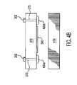
- FIG. 4Aillustrates the connections for attaching the printed filter assembly to a second printed circuit board.
- FIG. 4Billustrated details of connecting the printed filter assembly to a second printed circuit board.
- FIG. 5illustrates the apparatus used to mount a printed bandpass filter assembly to another printed circuit board.
- FIG. 6is a flow chart illustrating the steps used in designing a printed bandpass filter.
- the printed bandpass filter inventionis not limited to the tuner environment that is described herein, as the bandpass filter invention is applicable to other tuner and non-tuner applications as will be understood to those skilled in the relevant arts based on the discussions given herein.
- FIG. 1illustrates a double conversion tuner 100 .
- the double conversion tuner 100comprises a variable gain low noise amplifier 102 coupled to a first mixer 106 and a tuner input 101 .
- the first mixer 106is also coupled to a first local oscillator 104 .
- a high IF bandpass filter 108is coupled to the first mixer 106 and a second mixer 110 .
- the second mixer 110is coupled to a second local oscillator 112 and a second IF bandpass filter 114 .
- a variable gain amplifier 116is coupled to the second IF bandpass filter 114 and the tuner output 117 .
- the low noise amplifier 102amplifies a radio frequency (RF) signal 120 present at the tuner input 101 and sends it to the first mixer 106 .
- the RF signal 120is a television signal between approximately 50 and 850 megahertz.
- the first mixer 106combines the RF signal 120 with the output of the first local oscillator 104 and outputs a high IF signal 130 .
- the high IF signal 130comprises a signal at approximately 1220 megahertz and an image channel component at approximately 1132 megahertz.
- the high IF bandpass filter 108is a bandpass filter with its passband centered at approximately 1220 megahertz.
- the high IF signal 130is filtered by the high IF bandpass filter 108 .
- the high IF bandpass filter 108removes the image channel component and most of the undesired television channels. After filtering, the high IF signal 130 becomes a high filtered IF signal 135 . The high filtered IF signal 135 is mixed with the output of the second local oscillator 112 in the second mixer 110 to become a low IF signal 140 .
- the low IF signal 140comprises the television channels passed by the high IF bandpass filter 108 reduced in frequency to approximately 44 megahertz.
- the low IF signal 140at approximately 44 megahertz, is a standard television IF used in the United States.
- An embodiment of the double conversion tuner 100for use in Europe, produces the low IF final signal 140 at approximately 36 megahertz.
- the second IF bandpass filter 114removes the undesired television channels from the low IF signal 140 and outputs an IF signal 145 .
- the IF signal 145comprises the desired television channel and is sent to the variable gain amplifier 116 for amplification, then to the tuner output 117 .
- This inventionis a novel implementation of the high IF bandpass filter 108 using quarter wavelength resonators, coupled in parallel with a bypass line, and printed on a precision substrate.
- FIG. 2illustrates an electrical schematic of a bandpass filter 200 according to the present invention.
- the bandpass filter 200comprises an input capacitor 204 coupled to a filter input 202 , a bypass line input coupler 208 , a first resonator 206 , and a first intercoupler 210 .
- the first intercoupler 210is coupled to a second intercoupler 216 , and a second resonant element 214 .
- the second intercoupler 216is coupled to a bypass output coupler 218 , a third resonator 220 , and an output capacitor 222 .
- a bypass line 212is coupled to the bypass line input coupler 208 and the bypass line output coupler 218 .
- the output capacitor 222is coupled to the filter output 224 .
- the first resonator 206 , the second resonator 214 , and the third resonator 220are coupled to a ground 226 .
- the ground 226is located beneath the bandpass filter 200 .
- the printed metal tracescomprising the input capacitor 204 , first resonator 206 , first intercoupler 210 , second resonator 214 , second intercoupler 216 , third resonator 220 , output capacitor 222 , bypass line input coupler 208 , bypass line output coupler 218 , and bypass line 212 are microstrip transmission lines. Other equivalent transmission lines could be used.
- the input capacitor 204 and the output capacitor 222are printed finger capacitors. Printed finger capacitors are used to provide stronger capacitive coupling than is possible with transmission lines. The finger capacitors are simpler and less expensive than discreet surface mount capacitors and can be used on a single layer printed circuit board. The finger capacitors provide the necessary coupling capacitance without increasing the cost or complexity of the bandpass filter 200 . Capacitors, other than finger, could be utilized as would be understood by those skilled in the art.
- Adjusting the lengths of each resonator along with the inductive and capacitive characteristics of the coupled transmission lines, by incrementally adjusting the spacing, shape and width of each elementresults in a filter passband centered at a desired frequency and exhibiting a flat frequency response through the passband.
- the length, width, spacing and proximity to ground of the resonators and the transmission lines coupling the signal to and from the resonatorsdetermine the frequency response of the filter. If the printed circuit manufacturing process is well controlled, the physical dimensions of the resonators will not vary and post fabrication tuning will not be necessary.
- Rejection of the image channel component in the high IF signal 130can be improved by increasing the number of resonators in the filter. However, adding additional resonators will increase the signal insertion loss and the physical size of the filter.
- high IF signal 130passes from the filter input 202 through the input capacitor 204 , the first intercoupler 210 , and the second intercoupler 216 .
- the bypass line input coupler 208couples a bypass line signal 230 from the high IF signal 130 and feeds the delayed signal 230 forward through the bypass line 212 to the bypass line output coupler 218 .
- the bypass line input coupler 208 , the bypass line output coupler 218 , the first intercoupler 210 , and the second intercoupler 216each comprise a pair of coupled transmission lines.
- a coupled transmission linecan provide both inductive and capacitive coupling.
- the bypass line signal 230is modified to be approximately equal in amplitude and opposite in phase to the image channel component of high IF signal 130 .
- the output bypass line coupler 218couples the bypass line signal 230 with the high IF signal 130 , substantially attenuating the image channel component in the high IF signal 130 and sending the high filtered IF signal 135 through output capacitor 222 to the filter output 224 .
- This novel feed forward featureincreases image channel rejection by the printed bandpass filter 200 without significantly increasing the filter's insertion loss, physical size or component complexity.
- bandpass filter 200can attenuate components of the high IF signal 130 at frequencies other than the image channel frequency. This capability is built in to the bandpass filter 200 and provides means to further improve the filtered high IF signal 135 quality.
- FIG. 3Aillustrates a printed bandpass filter 300 which is a printed version of the bandpass filter 200 .
- the printed bandpass filter 300comprises an input capacitor 304 coupled to the filter input 202 , a bypass line input coupler 308 , a first resonator 306 , and a first intercoupler 310 .
- the first intercoupler 310is coupled to a second intercoupler 316 , and a second resonator 314 .
- the second intercoupler 316is coupled to a bypass line output coupler 318 , a third resonator 320 , and an output capacitor 322 .
- a bypass line 312is coupled to the bypass line input coupler 308 and the bypass line output coupler 318 .
- the output capacitor 322is coupled to the filter output 224 .
- the first resonator 306 , the second resonator 314 , and the third resonator 320are coupled to a ground 360 ( FIG. 3C ) by vias 375 a , 375 b , and 375 c .
- the via 375is a plated-through hole, electrically connecting portions of the printed filter 300 to the ground 360 .
- the input capacitor 304 and the output capacitor 322are printed finger capacitors.
- the bypass line input coupler 308 , the bypass line output coupler 318 , the first intercoupler 310 , and the second intercoupler 316are electromagnetically coupled segments of microstrip transmission line.
- the bypass line input coupler 308 , the bypass line output coupler 318 , the first intercoupler 310 , and the second intercoupler 316form a distributed transmission line implementation of the weak capacitive couplings used in a lumped-element LC bandpass filter.
- weak capacitive couplingis the capacitance present in the coupled transmission lines.
- this capacitanceis on the order of 0.2 pF.
- other values of capacitancecould be used as will be understood by one of ordinary skill in the relevant art.
- the ground 360is located beneath the filter 300 .
- the ground 360provides the return path necessary for bypass line input coupler 308 , the bypass line output coupler 318 , the first intercoupler 310 , the second intercoupler 316 , the first resonator 306 , the second resonator 314 , and the third resonator 320 to function as microstrip transmission lines.
- Additional embodiments of this invention, with or without the ground 360 under the bandpass filter 200can be implemented using coplanar waveguide transmission lines.
- the bypass line 312is a microstrip transmission line.
- the first resonator 306 , the second resonator 314 , and the third resonator 320each comprise a microstrip transmission line that is shorted at one end.
- the shorted transmission linepresents an open circuit to a signal applied at a resonant frequency.
- each resonatorShorting each resonator reduces the resonant length from one-half to one-quarter the wavelength of the desired resonant frequency.
- the one-quarter wavelength microstrip transmission linespresent an open-circuit at a resonant frequency, and together with the inherent weakly capacitive couplings are equivalent to a parallel LC tank circuit at the resonant frequency.
- the resonatorsare printed in the form of spirals on the substrate. Ideally, coupling between adjacent portions of the same resonator does not occur and the printed spiral is exactly one-quarter wavelength, of the desired resonant frequency, in size. Unfortunately, there is electromagnetic coupling between adjacent turns in each resonator spiral.
- the length of each resonator spiralis adjusted to become an open circuit through the desired passband. Therefore, in the present embodiment, the first resonator 306 , second resonator 314 , and the third resonator 320 are approximately one quarter wavelength in length.
- a quarter-wavelength resonatoris a resonator, coupled to ground on one end and becoming an open circuit at the chosen resonant frequency.
- the bypass line input coupler 308comprises an outer segment of the printed trace forming the first resonator 306 and a segment of the printed trace forming the bypass line 312 .
- a signal in the first resonator 306is coupled to the bypass line 312 by the electromagnetic coupling between these parallel trace segments of the first resonator 306 and the bypass line 312 .
- the bypass line output coupler 318comprises an outer segment of the printed trace forming the third resonator 320 and a section of the printed trace forming the bypass line 312 .
- the first intercoupler 310comprises another outer segment of the trace forming the first resonator 306 and an outer segment of the trace forming the second resonator 314 .
- the second intercoupler 316comprises an outer segment of the trace forming the second resonator 314 and an outer segment of the trace forming the third resonator 320 .
- the physical characteristics, trace width, length, and spacing, of the bypass line 312 , the input capacitor 304 , the bypass line input coupler 308 , the bypass line output coupler 318 , the first intercoupler 310 , the second intercoupler 316 , and the output capacitor 322are selected to cause the bypass line signal 230 to be approximately equal in amplitude and opposite in phase to the image channel component of high IF signal 130 .
- transmission linesin relation to each other and to electrical ground, determines whether the transmission line is classified as a coplanar waveguide or as a microstrip transmission line.
- Either type of transmission linecan be used in the present invention to achieve the size, simplicity and performance benefits discussed above.
- Impedance and electrical lengthdetermine the properties of a quarter-wavelength resonator.
- the substrate material chosenis GML-1000 (GIL Technologies, Collierville, Tenn.). Persons of skill in the art will recognize additional substrate materials that can be substituted to provide equivalent mechanical and electrical properties.
- Controlling the substrate's electrical and mechanical propertiesmakes the filter less susceptible to variations in the manufacturing process. It helps ensure repeatable behavior in the intercoupler sections, the bypass line input coupler and bypass line output coupler sections, and in the bypass line itself. Repeatability means the variations in electrical characteristics found in a lumped element bandpass filter are not present in the printed bandpass filter. As a result, there is no need to tune the present invention after fabrication. Eliminating the necessity to tune the filter between manufacture and installation is a significant reduction in manufacturing expense.
- Resonator to resonator couplingis accomplished by placing short segments of the resonators in close proximity to each other. This technique is also used to couple the bypass line 312 in the printed filter 300 using bypass line input coupler 308 and bypass line output coupler 318 . Coupling the filter input 202 and the filter output 224 to the printed filter 300 requires stronger coupling than can be achieved with transmission lines. Therefore, finger capacitors are used for the input capacitor 304 and the output capacitor 322 . The electrical properties of these capacitors are also well controlled if the substrate electrical and mechanical properties are well controlled.
- FIG. 3Billustrates a differential bandpass filter 350 .
- the differential bandpass filter 350comprises the printed bandpass filter 300 and a second printed bandpass filter 390 .
- the second printed bandpass filter 390comprises the mirror image of the printed bandpass filter 300 , a second filter input 302 and a second filter output 324 .
- the printed bandpass filter 300 and the second printed bandpass filter 390are printed on the same substrate in a manner to allow a differential signal to be applied to the filter input 202 and the second filter input 302 .
- the filtered differential signalis output at the filter output 224 and the second filter output 324 .
- the second printed bandpass filter 390functions similarly to the printed bandpass filter 300 .
- the differential bandpass filter 350enables a balanced signal to be used in tuner 100 .
- a balanced signalexhibits higher dynamic range, higher bandwidth, and lower pick-up and generation of interference noise than an unbalanced signal.
- FIG. 3Balso illustrates the required trace widths, trace lengths and trace spacings for an embodiment of the printed bandpass filter 300 .
- the input capacitor 304 and the output capacitor 322have calculated values of 0.19 pF.
- the differential bandpass filter 350has a Bandwidth of 1199 ⁇ 1240 M, an insertion loss of ⁇ 3 dB, a differential input and differential output impedance of 200 ohms and an image rejection of >40 dB.
- FIG. 3Balso illustrates one limitation on the ground 360 , printed on the opposite side of a substrate 370 (FIG. 3 C).
- the ungrounded zones 385 a , 385 b , 385 c , and 385 dare areas where the ground 360 is excluded to allow the high IF signal 130 and the filtered high IF signal 135 to be coupled to and from the differential bandpass filter 350 .
- FIG. 3Cillustrates a three-dimensional view of a printed filter assembly 380 .
- the filter assembly 380comprises a precision substrate 370 , the differential bandpass filter 350 printed on the upper side of the precision substrate 370 , and a ground 360 printed on the lower side of the precision substrate 370 .
- the ground 360is a metal pattern placed on the precision substrate 370 opposite the side the differential bandpass filter 350 is placed.
- One method of coupling the ground 360 to the differential bandpass filter 350is by the via 375 .
- the first resonator 306 , the second resonator 314 and the third resonator 320are coupled to the ground 360 by vias 375 a , 375 b , and 375 c respectively.
- the proximity of the differential bandpass filter 350 and the ground 360can cause a waveguide like effect in the precision substrate 370 .
- This effectresults in some portion of high IF signal 130 bypassing the differential bandpass filter 350 and increasing the out of band signal strength at filter output 224 and 324 . This effect is undesirable.
- FIG. 3Calso illustrates a plurality of vias 375 coupled between the ground 360 , a first blocking strip 376 and a second blocking strip 377 .
- the vias 375 , the blocking strips 376 and 377 and the ground 360act as shields to greatly reduce the IF signal leaking into the substrate.
- FIGS. 4A and 4Billustrate the differential bandpass filter 350 connections used when printed filter assembly 380 is mounted on a second printed circuit board 410 (FIG. 4 B).
- the second printed circuit board 410incorporates elements of the tuner 100 , and possibly other circuits, which are part of a larger assembly, including the tuner 100 .
- the filter input 202 , the filter second input 302 , the filter output 224 and the second filter output 324are connected to vias 375 a , 375 b , 375 c , and 375 d respectively.
- the vias 375are connected to the bottom (opposite) side of the precision substrate 370 .
- FIG. 4Bfurther illustrates a land pattern 420 used to connect the differential bandpass filter 350 to the second printed circuit board 410 .
- Coupling the printed filter assembly 380 to the second printed circuit board 410eliminates the need to use the relatively expensive precision substrate 370 for the second printed circuit board 410 .
- the via 375 ais coupled between the filter input 202 and the land pattern 420 a .
- the land pattern 420 acouples the positive component of high IF signal 130 from the second printed circuit board 410 to the filter input 202 .
- the via 375 bis coupled between the second filter input 302 and the land pattern 420 b .
- the land pattern 420 bcouples the negative component of high IF signal 130 from the second printed circuit board 410 to the second filter input 302 .
- the via 375 cis coupled between the filter output 224 and a corresponding (not shown) land pattern
- the via 375 dis coupled between the second filter output 324 and a corresponding land pattern (not shown). Additional vias 375 and land patterns 420 are used as necessary to route additional connections between the printed filter assembly 380 and the second printed circuit board 410 .
- the land pattern 420 and the ground 360coexist on the same side of the precision substrate 370 .
- the land pattern 420 and the ground 360are separated where necessary to couple a signal carrying element from the differential bandpass filter 350 to the land pattern 420 .
- the land pattern 420 and the ground 360are coupled where necessary to connect the ground 360 to the second printed circuit board 410 .
- FR-4is used for the printed circuit board 410 .
- the precision substrate 370has a slightly larger coefficient of thermal expansion than the printed circuit board material (FR-4). The difference in thermal expansion coefficient causes repetitive thermal stresses to be applied to the solder connections between the printed filter assembly 380 and the second printed circuit board 410 .
- FIG. 5illustrates an apparatus 500 for mitigating thermal cycling stress while maintaining the necessary electrical coupling between the differential bandpass filter 350 and the second printed circuit board 410 .
- the apparatus 500comprises a cup 515 coupled to a riser 510 , to abase 525 , and to a lower element 520 .
- One example of the apparatus 500is surface mount pin (model 34AC) by NAS Interplex, Flushing, N.Y.
- the apparatusis connected to the filter input 202 .
- Additional apparatus 500can be connected, as described below, to provide thermal stress relief for any connection between the printed filter assembly 380 and the second printed circuit board 410 . These connections comprise the second filter input 302 , the filter output 224 , the second filter output 324 , and ground 360 .
- the cup 515is connected to the filter input 202 and the lower element 520 is connected to the land pattern 420 .
- the cup 515is also coupled to via 375 which is coupled to land pattern 420 .
- the apparatus 500 and the via 375ensure a good electrical connection is maintained between the filter input 202 and the second printed circuit board 410 . Any differential thermal expansion is absorbed by deflection of the riser 510 vice deflection of an affected solder connection.
- the detailed design of the filteris accomplished using numerical optimization techniques.
- the structure of the filteris described in terms of coupled microstrip lines and input and output coupling capacitances using the RF circuit simulator MMICAD (Optotek Ltd., Kanata, Ontario, Canada), or any equivalent microwave circuit simulator with an optimizer.
- Lengths of the resonator and coupling sections, spacing of the coupled sections, input and output coupling capacitors, and length of the bypass lineare variables to be optimized (although approximate initial values were specified as a starting point).
- MMICADelectromagnetic finite-element simulation
- FIG. 6illustrates the steps of a method for printed bandpass filter design 600 .
- step 610the variable fitter design parameters used in the design are selected.
- step 620printed bandpass filter performance is simulated.
- step 640if simulated printed bandpass filter performance is equal to the filter design goal performance, step 630 is performed. If printed bandpass filter simulated performance is different from filter design goal performance, step 650 is performed.
- step 630the filter design is complete.
- the filter design parametersare incrementally varied in a manner to cause the simulated printed filter performance to approach the design goal performance. Steps 620 , 640 , and 650 are repeated until the simulated filter performance is equal to the design goal performance.
Landscapes
- Physics & Mathematics (AREA)
- Electromagnetism (AREA)
- Control Of Motors That Do Not Use Commutators (AREA)
- Networks Using Active Elements (AREA)
- Filters And Equalizers (AREA)
Abstract
Description
Claims (17)
Priority Applications (7)
| Application Number | Priority Date | Filing Date | Title |
|---|---|---|---|
| US10/040,376US7084720B2 (en) | 2002-01-09 | 2002-01-09 | Printed bandpass filter for a double conversion tuner |
| US10/295,985US7375604B2 (en) | 2002-01-09 | 2002-11-18 | Compact bandpass filter for double conversion tuner |
| EP03250090AEP1328039B1 (en) | 2002-01-09 | 2003-01-07 | Printed bandpass filter for a double conversion tuner |
| AT03250090TATE479214T1 (en) | 2002-01-09 | 2003-01-07 | PRINTED BANDPASS FILTER FOR DUAL MIX TUNING CIRCUIT |
| DE60333879TDE60333879D1 (en) | 2002-01-09 | 2003-01-07 | Printed bandpass filter for dual mix tuning circuit |
| US10/994,633US7071798B2 (en) | 2002-01-09 | 2004-11-23 | Printed bandpass filter for a double conversion tuner |
| US11/892,097US7567153B2 (en) | 2002-01-09 | 2007-08-20 | Compact bandpass filter for double conversion tuner |
Applications Claiming Priority (1)
| Application Number | Priority Date | Filing Date | Title |
|---|---|---|---|
| US10/040,376US7084720B2 (en) | 2002-01-09 | 2002-01-09 | Printed bandpass filter for a double conversion tuner |
Related Child Applications (2)
| Application Number | Title | Priority Date | Filing Date |
|---|---|---|---|
| US10/295,985Continuation-In-PartUS7375604B2 (en) | 2002-01-09 | 2002-11-18 | Compact bandpass filter for double conversion tuner |
| US10/994,633ContinuationUS7071798B2 (en) | 2002-01-09 | 2004-11-23 | Printed bandpass filter for a double conversion tuner |
Publications (2)
| Publication Number | Publication Date |
|---|---|
| US20030128085A1 US20030128085A1 (en) | 2003-07-10 |
| US7084720B2true US7084720B2 (en) | 2006-08-01 |
Family
ID=21910648
Family Applications (4)
| Application Number | Title | Priority Date | Filing Date |
|---|---|---|---|
| US10/040,376Expired - Fee RelatedUS7084720B2 (en) | 2002-01-09 | 2002-01-09 | Printed bandpass filter for a double conversion tuner |
| US10/295,985Expired - Fee RelatedUS7375604B2 (en) | 2002-01-09 | 2002-11-18 | Compact bandpass filter for double conversion tuner |
| US10/994,633Expired - Fee RelatedUS7071798B2 (en) | 2002-01-09 | 2004-11-23 | Printed bandpass filter for a double conversion tuner |
| US11/892,097Expired - Fee RelatedUS7567153B2 (en) | 2002-01-09 | 2007-08-20 | Compact bandpass filter for double conversion tuner |
Family Applications After (3)
| Application Number | Title | Priority Date | Filing Date |
|---|---|---|---|
| US10/295,985Expired - Fee RelatedUS7375604B2 (en) | 2002-01-09 | 2002-11-18 | Compact bandpass filter for double conversion tuner |
| US10/994,633Expired - Fee RelatedUS7071798B2 (en) | 2002-01-09 | 2004-11-23 | Printed bandpass filter for a double conversion tuner |
| US11/892,097Expired - Fee RelatedUS7567153B2 (en) | 2002-01-09 | 2007-08-20 | Compact bandpass filter for double conversion tuner |
Country Status (4)
| Country | Link |
|---|---|
| US (4) | US7084720B2 (en) |
| EP (1) | EP1328039B1 (en) |
| AT (1) | ATE479214T1 (en) |
| DE (1) | DE60333879D1 (en) |
Cited By (6)
| Publication number | Priority date | Publication date | Assignee | Title |
|---|---|---|---|---|
| US20050101274A1 (en)* | 2002-02-01 | 2005-05-12 | Koninklijke Philips Electronics N.V. | Television tuner and printed circuit board used therein |
| US20060141979A1 (en)* | 2004-12-23 | 2006-06-29 | Lianjun Liu | Radio frequency circuit with integrated on-chip radio frequency signal coupler |
| US20060141978A1 (en)* | 2004-12-23 | 2006-06-29 | Lianjun Liu | Compact radio frequency harmonic filter using integrated passive device technology |
| US20060170518A1 (en)* | 2005-02-01 | 2006-08-03 | Alpha Networks Inc. | Narrow bandpass filter installed on a circuit board for suppressing a high-frequency harmonic wave |
| US20080036557A1 (en)* | 2002-01-09 | 2008-02-14 | Broadcom Corporation | Compact bandpass filter for double conversion tuner |
| US20100188168A1 (en)* | 2009-01-27 | 2010-07-29 | Ding-Bing Lin | Wide band filter structure |
Families Citing this family (41)
| Publication number | Priority date | Publication date | Assignee | Title |
|---|---|---|---|---|
| US7460586B1 (en)* | 2004-08-17 | 2008-12-02 | Xilinx, Inc. | Selective signal coupling in high speed I/O circuits |
| TW200807799A (en)* | 2006-05-11 | 2008-02-01 | Koninkl Philips Electronics Nv | Resonator device with shorted stub and MIM-capacitor |
| US7468642B2 (en)* | 2006-12-12 | 2008-12-23 | International Business Machines Corporation | Multi band pass filters |
| US20100073107A1 (en)* | 2008-03-25 | 2010-03-25 | Superconductor Technologies Inc. | Micro-miniature monolithic electromagnetic resonators |
| US8107918B2 (en)* | 2008-04-11 | 2012-01-31 | Zoran Corporation | Broadband tuner for very wide signal conversion |
| FR2938379A1 (en)* | 2008-11-07 | 2010-05-14 | Commissariat Energie Atomique | DIFFERENTIAL FILTERING DEVICE WITH COPLANAR COUPLES AND FILTERING ANTENNA PROVIDED WITH SUCH A DEVICE |
| KR100987478B1 (en) | 2009-01-30 | 2010-10-13 | 한국항공대학교산학협력단 | Coplanar waveguide transmission line with multifrequency resonance |
| JP5604825B2 (en)* | 2009-08-19 | 2014-10-15 | ソニー株式会社 | Image processing apparatus and method |
| US8606207B2 (en)* | 2009-12-18 | 2013-12-10 | Broadcom Corporation | Fractal curve based filter |
| CN102569955B (en)* | 2012-01-18 | 2014-11-12 | 华南理工大学 | Dual-frequency band-pass filter based on asymmetric branch node loading resonator |
| US9899133B2 (en) | 2013-08-01 | 2018-02-20 | Qorvo Us, Inc. | Advanced 3D inductor structures with confined magnetic field |
| US9774311B2 (en)* | 2013-03-15 | 2017-09-26 | Qorvo Us, Inc. | Filtering characteristic adjustments of weakly coupled tunable RF filters |
| US9685928B2 (en) | 2013-08-01 | 2017-06-20 | Qorvo Us, Inc. | Interference rejection RF filters |
| US9391565B2 (en) | 2013-03-15 | 2016-07-12 | TriQuint International PTE, Ltd. | Amplifier phase distortion correction based on amplitude distortion measurement |
| US9755671B2 (en) | 2013-08-01 | 2017-09-05 | Qorvo Us, Inc. | VSWR detector for a tunable filter structure |
| US9825656B2 (en) | 2013-08-01 | 2017-11-21 | Qorvo Us, Inc. | Weakly coupled tunable RF transmitter architecture |
| US9871499B2 (en) | 2013-03-15 | 2018-01-16 | Qorvo Us, Inc. | Multi-band impedance tuners using weakly-coupled LC resonators |
| US12224096B2 (en) | 2013-03-15 | 2025-02-11 | Qorvo Us, Inc. | Advanced 3D inductor structures with confined magnetic field |
| US9628045B2 (en) | 2013-08-01 | 2017-04-18 | Qorvo Us, Inc. | Cooperative tunable RF filters |
| US9705478B2 (en) | 2013-08-01 | 2017-07-11 | Qorvo Us, Inc. | Weakly coupled tunable RF receiver architecture |
| US9866197B2 (en) | 2013-06-06 | 2018-01-09 | Qorvo Us, Inc. | Tunable RF filter based RF communications system |
| US9859863B2 (en) | 2013-03-15 | 2018-01-02 | Qorvo Us, Inc. | RF filter structure for antenna diversity and beam forming |
| US9780756B2 (en) | 2013-08-01 | 2017-10-03 | Qorvo Us, Inc. | Calibration for a tunable RF filter structure |
| US9705542B2 (en) | 2013-06-06 | 2017-07-11 | Qorvo Us, Inc. | Reconfigurable RF filter |
| US9780817B2 (en) | 2013-06-06 | 2017-10-03 | Qorvo Us, Inc. | RX shunt switching element-based RF front-end circuit |
| US9800282B2 (en) | 2013-06-06 | 2017-10-24 | Qorvo Us, Inc. | Passive voltage-gain network |
| US9966981B2 (en) | 2013-06-06 | 2018-05-08 | Qorvo Us, Inc. | Passive acoustic resonator based RF receiver |
| TWI478636B (en)* | 2013-08-09 | 2015-03-21 | Hon Hai Prec Ind Co Ltd | Printed circuit board |
| CN104378908B (en)* | 2013-08-12 | 2017-06-16 | 鸿富锦精密工业(深圳)有限公司 | Printed circuit board (PCB) |
| CN104009271B (en)* | 2014-05-12 | 2016-04-13 | 华南理工大学 | Planar band-pass filter based on four cascaded resonators |
| CN104966871A (en)* | 2015-07-13 | 2015-10-07 | 南京恒电电子有限公司 | Microstrip planar spiral filter and design method thereof |
| US10796835B2 (en) | 2015-08-24 | 2020-10-06 | Qorvo Us, Inc. | Stacked laminate inductors for high module volume utilization and performance-cost-size-processing-time tradeoff |
| US11139238B2 (en) | 2016-12-07 | 2021-10-05 | Qorvo Us, Inc. | High Q factor inductor structure |
| KR101870201B1 (en)* | 2017-03-03 | 2018-06-22 | 광운대학교 산학협력단 | A compact bandstop filter using frequency-selecting coupling structure with interdigital and spiral types |
| RU2672821C1 (en)* | 2017-10-30 | 2018-11-19 | Федеральное государственное бюджетное образовательное учреждение высшего образования "Сибирский государственный университет науки и технологий имени академика М.Ф. Решетнева" (СибГУ им. М.Ф. Решетнева) | Band pass filter |
| RU182125U1 (en)* | 2017-12-26 | 2018-08-03 | Федеральное государственное автономное образовательное учреждение высшего образования "Уральский федеральный университет имени первого Президента России Б.Н. Ельцина" | MICRO-STRIP BAND FILTER |
| WO2020154008A1 (en)* | 2019-01-25 | 2020-07-30 | Commscope Italy S.R.L. | Multi-pole rf filters |
| CN109841933B (en)* | 2019-03-11 | 2021-07-09 | 南通大学 | A compact wideband differential bandpass filter |
| TWI715478B (en)* | 2020-03-30 | 2021-01-01 | 財團法人工業技術研究院 | Filter |
| US11862835B2 (en)* | 2020-08-13 | 2024-01-02 | Cyntec Co., Ltd. | Dielectric filter with multilayer resonator |
| WO2025093112A1 (en)* | 2023-10-31 | 2025-05-08 | Telefonaktiebolaget Lm Ericsson (Publ) | Multi-band filter and an antenna system comprising a multi-band filter |
Citations (36)
| Publication number | Priority date | Publication date | Assignee | Title |
|---|---|---|---|---|
| US4418324A (en) | 1981-12-31 | 1983-11-29 | Motorola, Inc. | Implementation of a tunable transmission zero on transmission line filters |
| US4423396A (en)* | 1980-09-30 | 1983-12-27 | Matsushita Electric Industrial Company, Limited | Bandpass filter for UHF band |
| US4488130A (en)* | 1983-02-24 | 1984-12-11 | Hughes Aircraft Company | Microwave integrated circuit, bandpass filter |
| US4740765A (en) | 1985-09-30 | 1988-04-26 | Murata Manufacturing Co., Ltd. | Dielectric filter |
| US4757285A (en)* | 1986-07-29 | 1988-07-12 | Siemens Aktiengesellschaft | Filter for short electromagnetic waves formed as a comb line or interdigital line filters |
| US4801905A (en)* | 1987-04-23 | 1989-01-31 | Hewlett-Packard Company | Microstrip shielding system |
| US4881043A (en) | 1988-09-12 | 1989-11-14 | Motorola, Inc. | Variable gain transconductance amplifier and variable bandwidth filter |
| EP0506476A1 (en) | 1991-03-29 | 1992-09-30 | Ngk Insulators, Ltd. | Dielectric filter having coupling electrodes for connecting resonator electrodes, and method of adjusting frequency characteristic of the filter |
| US5192926A (en)* | 1990-01-17 | 1993-03-09 | Fujitsu Limited | Dielectric filter with attenuation poles |
| JPH05308204A (en) | 1992-04-30 | 1993-11-19 | Ngk Spark Plug Co Ltd | Adjustment method for attenuation pole for strip line filter |
| JPH0865007A (en) | 1994-08-22 | 1996-03-08 | Murata Mfg Co Ltd | High frequency filter |
| US5739193A (en) | 1996-05-07 | 1998-04-14 | Hoechst Celanese Corp. | Polymeric compositions having a temperature-stable dielectric constant |
| US5825263A (en) | 1996-10-11 | 1998-10-20 | Northern Telecom Limited | Low radiation balanced microstrip bandpass filter |
| US5896073A (en) | 1996-02-20 | 1999-04-20 | Mitsubishi Denki Kabushiki Kaisha | High frequency filter having a plurality of serially coupled first resonators and a second resonator |
| US5949295A (en) | 1993-06-29 | 1999-09-07 | Sican, Gesellschaft Fur Silizium-Anwendungen Und Cad/Cat Niedersachsen Mbh | Integratable tunable resonant circuit for use in filters and oscillators |
| US5955931A (en) | 1995-01-09 | 1999-09-21 | Murata Manufacturing Co., Ltd. | Chip type filter with electromagnetically coupled resonators |
| US5986525A (en) | 1996-11-08 | 1999-11-16 | Murata Manufacturing Co., Ltd. | Filter device having a distributed-constant-line-type resonator |
| JPH11317603A (en) | 1998-02-27 | 1999-11-16 | Matsushita Electric Ind Co Ltd | Balanced dielectric filter |
| US6100761A (en) | 1998-10-07 | 2000-08-08 | Microtune, Inc. | Highly linear variable-gain low noise amplifier |
| US6108569A (en)* | 1998-05-15 | 2000-08-22 | E. I. Du Pont De Nemours And Company | High temperature superconductor mini-filters and mini-multiplexers with self-resonant spiral resonators |
| US6130189A (en) | 1996-06-17 | 2000-10-10 | Superconductor Technologies, Inc. | Microwave hairpin-comb filters for narrow-band applications |
| US6130591A (en) | 1997-08-25 | 2000-10-10 | Advanced Mobile Telecommunication Technology Inc. | Band-pass filter comprising series coupled split gap resonators arranged along a circular position line |
| US6191665B1 (en)* | 1998-05-29 | 2001-02-20 | Motorola, Inc. | Coupling circuit to reduce intermodulation distortion in radiofrequency receivers |
| US6252476B1 (en) | 2000-04-19 | 2001-06-26 | Rockwell Collins, Inc. | Microstrip resonators and coupled line bandpass filters using same |
| US6259752B1 (en)* | 2000-02-01 | 2001-07-10 | Conexant Systems, Inc. | System for cancelling internal interference in a receiver |
| US6288609B1 (en) | 2000-02-29 | 2001-09-11 | Motorola, Inc. | Gain controllable low noise amplifier with automatic linearity enhancement and method of doing same |
| US6411181B1 (en) | 1999-02-23 | 2002-06-25 | Murata Manufacturing Co., Ltd. | Dielectric resonator, inductor, capacitor, dielectric filter, oscillator, and communication device |
| US6438394B1 (en)* | 1994-10-14 | 2002-08-20 | Conductus, Inc. | Frequency dependent inductor apparatus and method for a narrow-band filter |
| US6448640B2 (en) | 1999-09-02 | 2002-09-10 | Micron Technology, Inc. | Ball array layout in chip assembly |
| US6448873B1 (en)* | 1998-01-09 | 2002-09-10 | Texas Instruments Incorporated | LC filter with suspended printed inductor and compensating interdigital capacitor |
| US6486754B1 (en)* | 1998-12-22 | 2002-11-26 | Murata Manufacturing Co., Ltd. | Resonator, filter, duplexer, and communication device |
| US6496710B1 (en) | 2000-04-24 | 2002-12-17 | Cryodevice Inc. | Signal filter having circularly arranged resonators |
| US6522217B1 (en)* | 1999-12-01 | 2003-02-18 | E. I. Du Pont De Nemours And Company | Tunable high temperature superconducting filter |
| US6597265B2 (en) | 2000-11-14 | 2003-07-22 | Paratek Microwave, Inc. | Hybrid resonator microstrip line filters |
| US6639909B1 (en) | 1998-09-17 | 2003-10-28 | Nec Corporation | Receiver having functions for cancelling DC offset and measuring carrier detection threshold value, and control method thereof |
| US6771774B1 (en) | 1999-12-02 | 2004-08-03 | Tut Systems, Inc. | Filter arrangement for shaping a pulse propagated over pots wiring, and a method of manufacturing the same |
Family Cites Families (8)
| Publication number | Priority date | Publication date | Assignee | Title |
|---|---|---|---|---|
| US641181A (en)* | 1896-02-21 | 1900-01-09 | Carlostine E Blake | Automatic coupling for air-pumps. |
| US4423896A (en)* | 1981-03-06 | 1984-01-03 | Unarco Industries, Inc. | Replacement hasp, kit, and method for replacing railroad car lock hasps |
| DE3132930A1 (en)* | 1981-08-20 | 1983-03-03 | Licentia Patent-Verwaltungs-Gmbh, 6000 Frankfurt | Microwave filter using stripline technology |
| US5739198A (en)* | 1996-03-18 | 1998-04-14 | The Goodyear Tire & Rubber Company | Rubber composition and tire with tread thereof |
| JP3466400B2 (en)* | 1996-12-24 | 2003-11-10 | 京セラ株式会社 | filter |
| JPH11176491A (en)* | 1997-10-07 | 1999-07-02 | Seiko Instruments Inc | Electronic device charging system |
| US7084720B2 (en)* | 2002-01-09 | 2006-08-01 | Broadcom Corporation | Printed bandpass filter for a double conversion tuner |
| US6700459B2 (en)* | 2002-05-29 | 2004-03-02 | Superconductor Technologies, Inc. | Dual-mode bandpass filter with direct capacitive couplings and far-field suppression structures |
- 2002
- 2002-01-09USUS10/040,376patent/US7084720B2/ennot_activeExpired - Fee Related
- 2002-11-18USUS10/295,985patent/US7375604B2/ennot_activeExpired - Fee Related
- 2003
- 2003-01-07ATAT03250090Tpatent/ATE479214T1/ennot_activeIP Right Cessation
- 2003-01-07DEDE60333879Tpatent/DE60333879D1/ennot_activeExpired - Lifetime
- 2003-01-07EPEP03250090Apatent/EP1328039B1/ennot_activeExpired - Lifetime
- 2004
- 2004-11-23USUS10/994,633patent/US7071798B2/ennot_activeExpired - Fee Related
- 2007
- 2007-08-20USUS11/892,097patent/US7567153B2/ennot_activeExpired - Fee Related
Patent Citations (36)
| Publication number | Priority date | Publication date | Assignee | Title |
|---|---|---|---|---|
| US4423396A (en)* | 1980-09-30 | 1983-12-27 | Matsushita Electric Industrial Company, Limited | Bandpass filter for UHF band |
| US4418324A (en) | 1981-12-31 | 1983-11-29 | Motorola, Inc. | Implementation of a tunable transmission zero on transmission line filters |
| US4488130A (en)* | 1983-02-24 | 1984-12-11 | Hughes Aircraft Company | Microwave integrated circuit, bandpass filter |
| US4740765A (en) | 1985-09-30 | 1988-04-26 | Murata Manufacturing Co., Ltd. | Dielectric filter |
| US4757285A (en)* | 1986-07-29 | 1988-07-12 | Siemens Aktiengesellschaft | Filter for short electromagnetic waves formed as a comb line or interdigital line filters |
| US4801905A (en)* | 1987-04-23 | 1989-01-31 | Hewlett-Packard Company | Microstrip shielding system |
| US4881043A (en) | 1988-09-12 | 1989-11-14 | Motorola, Inc. | Variable gain transconductance amplifier and variable bandwidth filter |
| US5192926A (en)* | 1990-01-17 | 1993-03-09 | Fujitsu Limited | Dielectric filter with attenuation poles |
| EP0506476A1 (en) | 1991-03-29 | 1992-09-30 | Ngk Insulators, Ltd. | Dielectric filter having coupling electrodes for connecting resonator electrodes, and method of adjusting frequency characteristic of the filter |
| JPH05308204A (en) | 1992-04-30 | 1993-11-19 | Ngk Spark Plug Co Ltd | Adjustment method for attenuation pole for strip line filter |
| US5949295A (en) | 1993-06-29 | 1999-09-07 | Sican, Gesellschaft Fur Silizium-Anwendungen Und Cad/Cat Niedersachsen Mbh | Integratable tunable resonant circuit for use in filters and oscillators |
| JPH0865007A (en) | 1994-08-22 | 1996-03-08 | Murata Mfg Co Ltd | High frequency filter |
| US6438394B1 (en)* | 1994-10-14 | 2002-08-20 | Conductus, Inc. | Frequency dependent inductor apparatus and method for a narrow-band filter |
| US5955931A (en) | 1995-01-09 | 1999-09-21 | Murata Manufacturing Co., Ltd. | Chip type filter with electromagnetically coupled resonators |
| US5896073A (en) | 1996-02-20 | 1999-04-20 | Mitsubishi Denki Kabushiki Kaisha | High frequency filter having a plurality of serially coupled first resonators and a second resonator |
| US5739193A (en) | 1996-05-07 | 1998-04-14 | Hoechst Celanese Corp. | Polymeric compositions having a temperature-stable dielectric constant |
| US6130189A (en) | 1996-06-17 | 2000-10-10 | Superconductor Technologies, Inc. | Microwave hairpin-comb filters for narrow-band applications |
| US5825263A (en) | 1996-10-11 | 1998-10-20 | Northern Telecom Limited | Low radiation balanced microstrip bandpass filter |
| US5986525A (en) | 1996-11-08 | 1999-11-16 | Murata Manufacturing Co., Ltd. | Filter device having a distributed-constant-line-type resonator |
| US6130591A (en) | 1997-08-25 | 2000-10-10 | Advanced Mobile Telecommunication Technology Inc. | Band-pass filter comprising series coupled split gap resonators arranged along a circular position line |
| US6448873B1 (en)* | 1998-01-09 | 2002-09-10 | Texas Instruments Incorporated | LC filter with suspended printed inductor and compensating interdigital capacitor |
| JPH11317603A (en) | 1998-02-27 | 1999-11-16 | Matsushita Electric Ind Co Ltd | Balanced dielectric filter |
| US6108569A (en)* | 1998-05-15 | 2000-08-22 | E. I. Du Pont De Nemours And Company | High temperature superconductor mini-filters and mini-multiplexers with self-resonant spiral resonators |
| US6191665B1 (en)* | 1998-05-29 | 2001-02-20 | Motorola, Inc. | Coupling circuit to reduce intermodulation distortion in radiofrequency receivers |
| US6639909B1 (en) | 1998-09-17 | 2003-10-28 | Nec Corporation | Receiver having functions for cancelling DC offset and measuring carrier detection threshold value, and control method thereof |
| US6100761A (en) | 1998-10-07 | 2000-08-08 | Microtune, Inc. | Highly linear variable-gain low noise amplifier |
| US6486754B1 (en)* | 1998-12-22 | 2002-11-26 | Murata Manufacturing Co., Ltd. | Resonator, filter, duplexer, and communication device |
| US6411181B1 (en) | 1999-02-23 | 2002-06-25 | Murata Manufacturing Co., Ltd. | Dielectric resonator, inductor, capacitor, dielectric filter, oscillator, and communication device |
| US6448640B2 (en) | 1999-09-02 | 2002-09-10 | Micron Technology, Inc. | Ball array layout in chip assembly |
| US6522217B1 (en)* | 1999-12-01 | 2003-02-18 | E. I. Du Pont De Nemours And Company | Tunable high temperature superconducting filter |
| US6771774B1 (en) | 1999-12-02 | 2004-08-03 | Tut Systems, Inc. | Filter arrangement for shaping a pulse propagated over pots wiring, and a method of manufacturing the same |
| US6259752B1 (en)* | 2000-02-01 | 2001-07-10 | Conexant Systems, Inc. | System for cancelling internal interference in a receiver |
| US6288609B1 (en) | 2000-02-29 | 2001-09-11 | Motorola, Inc. | Gain controllable low noise amplifier with automatic linearity enhancement and method of doing same |
| US6252476B1 (en) | 2000-04-19 | 2001-06-26 | Rockwell Collins, Inc. | Microstrip resonators and coupled line bandpass filters using same |
| US6496710B1 (en) | 2000-04-24 | 2002-12-17 | Cryodevice Inc. | Signal filter having circularly arranged resonators |
| US6597265B2 (en) | 2000-11-14 | 2003-07-22 | Paratek Microwave, Inc. | Hybrid resonator microstrip line filters |
Non-Patent Citations (7)
| Title |
|---|
| European Patent Office English-language Abstract fo JP 11317603, published Nov. 16, 1999, 1 page. |
| European Patent Office English-language Abstract for JP 05308204, published Nov. 19, 1993, 1 page. |
| European Patent Office English-language Abstract for JP 08065007, published Mar. 8, 1996, 1 page. |
| European Search Report from European Patent Application No. 03250090.2, dated Jan. 14, 2004, 3 pages. |
| GIL Technologies, GML 1000 High Frequency Laminate, at http://www.shfmicro.com/gil20.pdf, 1 page (date unknown). |
| Kuo, J.-T., et al., "Microstrip Elliptic Function Filters with Compact Miniaturized Hairpin Resonators," IEEE, pp. 861-864 (1999). |
| Matthaei, G. et al., Microwave Filters, Impedence-Matching Networks and Coupling Structures, Artech House, Inc., entire book submitted (1980). |
Cited By (11)
| Publication number | Priority date | Publication date | Assignee | Title |
|---|---|---|---|---|
| US20080036557A1 (en)* | 2002-01-09 | 2008-02-14 | Broadcom Corporation | Compact bandpass filter for double conversion tuner |
| US7567153B2 (en) | 2002-01-09 | 2009-07-28 | Broadcom Corporation | Compact bandpass filter for double conversion tuner |
| US20050101274A1 (en)* | 2002-02-01 | 2005-05-12 | Koninklijke Philips Electronics N.V. | Television tuner and printed circuit board used therein |
| US7319497B2 (en)* | 2002-02-01 | 2008-01-15 | Nxp B.V. | Printed circuit board configurable television tuner |
| US20060141979A1 (en)* | 2004-12-23 | 2006-06-29 | Lianjun Liu | Radio frequency circuit with integrated on-chip radio frequency signal coupler |
| US20060141978A1 (en)* | 2004-12-23 | 2006-06-29 | Lianjun Liu | Compact radio frequency harmonic filter using integrated passive device technology |
| US7305223B2 (en)* | 2004-12-23 | 2007-12-04 | Freescale Semiconductor, Inc. | Radio frequency circuit with integrated on-chip radio frequency signal coupler |
| US7418251B2 (en)* | 2004-12-23 | 2008-08-26 | Freescale Semiconductor, Inc. | Compact radio frequency harmonic filter using integrated passive device technology |
| US20060170518A1 (en)* | 2005-02-01 | 2006-08-03 | Alpha Networks Inc. | Narrow bandpass filter installed on a circuit board for suppressing a high-frequency harmonic wave |
| US7221240B2 (en)* | 2005-02-01 | 2007-05-22 | Alpha Networks Inc. | Narrow bandpass filter installed on a circuit board for suppressing a high-frequency harmonic wave |
| US20100188168A1 (en)* | 2009-01-27 | 2010-07-29 | Ding-Bing Lin | Wide band filter structure |
Also Published As
| Publication number | Publication date |
|---|---|
| US20030128085A1 (en) | 2003-07-10 |
| ATE479214T1 (en) | 2010-09-15 |
| US7375604B2 (en) | 2008-05-20 |
| US20080036557A1 (en) | 2008-02-14 |
| DE60333879D1 (en) | 2010-10-07 |
| EP1328039A3 (en) | 2004-02-25 |
| EP1328039B1 (en) | 2010-08-25 |
| EP1328039A2 (en) | 2003-07-16 |
| US7071798B2 (en) | 2006-07-04 |
| US20030128084A1 (en) | 2003-07-10 |
| US20050093661A1 (en) | 2005-05-05 |
| US7567153B2 (en) | 2009-07-28 |
Similar Documents
| Publication | Publication Date | Title |
|---|---|---|
| US7084720B2 (en) | Printed bandpass filter for a double conversion tuner | |
| US5543764A (en) | Filter having an electromagnetically tunable transmission zero | |
| Bonache et al. | Novel microstrip bandpass filters based on complementary split-ring resonators | |
| US6215374B1 (en) | Magnetically coupled resonators for achieving low cost narrow band pass filters having high selectivity, low insertion loss and improved out-of-band rejection | |
| US7012484B2 (en) | Filter using multilayer ceramic technology and structure thereof | |
| US5343176A (en) | Radio frequency filter having a substrate with recessed areas | |
| AU1935200A (en) | Narrow band-pass tuned resonator filter topologies having high selectivity, low insertion loss and improved out-of band rejection over extended frequency ranges | |
| US6091312A (en) | Semi-lumped bandstop filter | |
| US6064281A (en) | Semi-lumped bandpass filter | |
| US20050190016A1 (en) | [parallel-coupled-resonator filter with open-and-short end] | |
| FI89991C (en) | HOEGFREKVENSBANDPASSFILTER | |
| KR101250060B1 (en) | Electrically tunable bandpass filters | |
| US20040023628A1 (en) | Ultra-selective broadband bandpass filter using hybrid technology | |
| WO1997007556A1 (en) | Ceramic filter with ground plane features which provide transmission zero and coupling adjustment | |
| US20040183626A1 (en) | Electronically tunable block filter with tunable transmission zeros | |
| WO2008089197A2 (en) | Integrated bandpass/bandstop coupled line filter | |
| Ye et al. | Design of ultra-wideband bandpass (UWB) filter with enhanced couplings by using lumped capacitors | |
| GB2302453A (en) | Dielectric filter | |
| Fernández‐Prieto et al. | COUPLED‐RESONATOR BALANCED BANDPASS FILTERS WITH COMMON‐MODE SUPPRESSION DIFFERENTIAL LINES | |
| US20250112351A1 (en) | Microwave band-pass filter with wide stopband using l-shaped slotted microstrip resonators | |
| Elsheikh et al. | Strip-loaded coplanar waveguide bandpass filter with wideband spur-free response | |
| Xu et al. | Lumped LTCC Coupler with Inductor and Capacitor surrounded Resonators | |
| Arjun et al. | Design of a Compact Distributed-Lumped Ka-Band BPF with Wide Stopband in IPD Technology | |
| US20040113724A1 (en) | Integrated and tunable high quality resonant circuit based on transmission lines | |
| JP2002158503A (en) | Bandpass filter |
Legal Events
| Date | Code | Title | Description |
|---|---|---|---|
| AS | Assignment | Owner name:BROADCOM CORPORATION, CALIFORNIA Free format text:ASSIGNMENT OF ASSIGNORS INTEREST;ASSIGNORS:GOMEZ, RAMON A.;BURNS, LAWRENCE M.;CHANG, SUNG-HSIEN;AND OTHERS;REEL/FRAME:012473/0317;SIGNING DATES FROM 20011220 TO 20020107 | |
| FPAY | Fee payment | Year of fee payment:4 | |
| REMI | Maintenance fee reminder mailed | ||
| LAPS | Lapse for failure to pay maintenance fees | ||
| STCH | Information on status: patent discontinuation | Free format text:PATENT EXPIRED DUE TO NONPAYMENT OF MAINTENANCE FEES UNDER 37 CFR 1.362 | |
| FP | Lapsed due to failure to pay maintenance fee | Effective date:20140801 | |
| AS | Assignment | Owner name:BANK OF AMERICA, N.A., AS COLLATERAL AGENT, NORTH CAROLINA Free format text:PATENT SECURITY AGREEMENT;ASSIGNOR:BROADCOM CORPORATION;REEL/FRAME:037806/0001 Effective date:20160201 Owner name:BANK OF AMERICA, N.A., AS COLLATERAL AGENT, NORTH Free format text:PATENT SECURITY AGREEMENT;ASSIGNOR:BROADCOM CORPORATION;REEL/FRAME:037806/0001 Effective date:20160201 | |
| AS | Assignment | Owner name:AVAGO TECHNOLOGIES GENERAL IP (SINGAPORE) PTE. LTD., SINGAPORE Free format text:ASSIGNMENT OF ASSIGNORS INTEREST;ASSIGNOR:BROADCOM CORPORATION;REEL/FRAME:041706/0001 Effective date:20170120 Owner name:AVAGO TECHNOLOGIES GENERAL IP (SINGAPORE) PTE. LTD Free format text:ASSIGNMENT OF ASSIGNORS INTEREST;ASSIGNOR:BROADCOM CORPORATION;REEL/FRAME:041706/0001 Effective date:20170120 | |
| AS | Assignment | Owner name:BROADCOM CORPORATION, CALIFORNIA Free format text:TERMINATION AND RELEASE OF SECURITY INTEREST IN PATENTS;ASSIGNOR:BANK OF AMERICA, N.A., AS COLLATERAL AGENT;REEL/FRAME:041712/0001 Effective date:20170119 |