US7084475B2 - Lateral conduction Schottky diode with plural mesas - Google Patents
Lateral conduction Schottky diode with plural mesasDownload PDFInfo
- Publication number
- US7084475B2 US7084475B2US10/780,363US78036304AUS7084475B2US 7084475 B2US7084475 B2US 7084475B2US 78036304 AUS78036304 AUS 78036304AUS 7084475 B2US7084475 B2US 7084475B2
- Authority
- US
- United States
- Prior art keywords
- submount
- schottky diode
- contacts
- mesas
- semiconductor layer
- Prior art date
- Legal status (The legal status is an assumption and is not a legal conclusion. Google has not performed a legal analysis and makes no representation as to the accuracy of the status listed.)
- Expired - Lifetime, expires
Links
- 239000004065semiconductorSubstances0.000claimsdescription144
- 239000000758substrateSubstances0.000claimsdescription79
- 229910052751metalInorganic materials0.000claimsdescription58
- 239000002184metalSubstances0.000claimsdescription58
- 239000004020conductorSubstances0.000claimsdescription27
- 150000004767nitridesChemical class0.000claimsdescription23
- 229910002601GaNInorganic materials0.000claimsdescription19
- JMASRVWKEDWRBT-UHFFFAOYSA-NGallium nitrideChemical compound[Ga]#NJMASRVWKEDWRBT-UHFFFAOYSA-N0.000claimsdescription17
- 230000020169heat generationEffects0.000abstract1
- 239000000463materialSubstances0.000description18
- 239000010931goldSubstances0.000description13
- 229910052710siliconInorganic materials0.000description11
- XUIMIQQOPSSXEZ-UHFFFAOYSA-NSiliconChemical compound[Si]XUIMIQQOPSSXEZ-UHFFFAOYSA-N0.000description10
- BASFCYQUMIYNBI-UHFFFAOYSA-NplatinumChemical compound[Pt]BASFCYQUMIYNBI-UHFFFAOYSA-N0.000description10
- 239000010703siliconSubstances0.000description10
- 229910000679solderInorganic materials0.000description10
- PCHJSUWPFVWCPO-UHFFFAOYSA-NgoldChemical compound[Au]PCHJSUWPFVWCPO-UHFFFAOYSA-N0.000description6
- 229910052737goldInorganic materials0.000description6
- 238000000034methodMethods0.000description6
- 239000002019doping agentSubstances0.000description5
- PXHVJJICTQNCMI-UHFFFAOYSA-NNickelChemical compound[Ni]PXHVJJICTQNCMI-UHFFFAOYSA-N0.000description4
- KDLHZDBZIXYQEI-UHFFFAOYSA-NPalladiumChemical compound[Pd]KDLHZDBZIXYQEI-UHFFFAOYSA-N0.000description4
- 229910052782aluminiumInorganic materials0.000description4
- XAGFODPZIPBFFR-UHFFFAOYSA-NaluminiumChemical compound[Al]XAGFODPZIPBFFR-UHFFFAOYSA-N0.000description4
- 239000010936titaniumSubstances0.000description4
- GYHNNYVSQQEPJS-UHFFFAOYSA-NGalliumChemical compound[Ga]GYHNNYVSQQEPJS-UHFFFAOYSA-N0.000description3
- 230000008901benefitEffects0.000description3
- 229910052733galliumInorganic materials0.000description3
- 238000004806packaging method and processMethods0.000description3
- 229910052697platinumInorganic materials0.000description3
- 230000007480spreadingEffects0.000description3
- QGZKDVFQNNGYKY-UHFFFAOYSA-NAmmoniaChemical compoundNQGZKDVFQNNGYKY-UHFFFAOYSA-N0.000description2
- IJGRMHOSHXDMSA-UHFFFAOYSA-NAtomic nitrogenChemical compoundN#NIJGRMHOSHXDMSA-UHFFFAOYSA-N0.000description2
- RTAQQCXQSZGOHL-UHFFFAOYSA-NTitaniumChemical compound[Ti]RTAQQCXQSZGOHL-UHFFFAOYSA-N0.000description2
- 238000003877atomic layer epitaxyMethods0.000description2
- 230000004888barrier functionEffects0.000description2
- 150000001875compoundsChemical class0.000description2
- 239000013078crystalSubstances0.000description2
- 230000007547defectEffects0.000description2
- 239000007789gasSubstances0.000description2
- 230000017525heat dissipationEffects0.000description2
- 150000002739metalsChemical class0.000description2
- 238000001451molecular beam epitaxyMethods0.000description2
- 238000002161passivationMethods0.000description2
- 230000008569processEffects0.000description2
- 238000005546reactive sputteringMethods0.000description2
- HBMJWWWQQXIZIP-UHFFFAOYSA-Nsilicon carbideChemical compound[Si+]#[C-]HBMJWWWQQXIZIP-UHFFFAOYSA-N0.000description2
- 229910010271silicon carbideInorganic materials0.000description2
- 239000002470thermal conductorSubstances0.000description2
- 229910052719titaniumInorganic materials0.000description2
- 229910016420Ala InbInorganic materials0.000description1
- PIGFYZPCRLYGLF-UHFFFAOYSA-NAluminum nitrideChemical compound[Al]#NPIGFYZPCRLYGLF-UHFFFAOYSA-N0.000description1
- 229910021529ammoniaInorganic materials0.000description1
- 238000000429assemblyMethods0.000description1
- 230000000712assemblyEffects0.000description1
- 230000015572biosynthetic processEffects0.000description1
- 230000015556catabolic processEffects0.000description1
- 238000005229chemical vapour depositionMethods0.000description1
- 239000002131composite materialSubstances0.000description1
- 239000000470constituentSubstances0.000description1
- 239000002178crystalline materialSubstances0.000description1
- 238000010586diagramMethods0.000description1
- 229910003460diamondInorganic materials0.000description1
- 239000010432diamondSubstances0.000description1
- 230000000694effectsEffects0.000description1
- 238000005530etchingMethods0.000description1
- 229910052738indiumInorganic materials0.000description1
- APFVFJFRJDLVQX-UHFFFAOYSA-Nindium atomChemical compound[In]APFVFJFRJDLVQX-UHFFFAOYSA-N0.000description1
- 230000004048modificationEffects0.000description1
- 238000012986modificationMethods0.000description1
- 229910052759nickelInorganic materials0.000description1
- 229910052757nitrogenInorganic materials0.000description1
- QJGQUHMNIGDVPM-UHFFFAOYSA-Nnitrogen groupChemical group[N]QJGQUHMNIGDVPM-UHFFFAOYSA-N0.000description1
- 150000002894organic compoundsChemical class0.000description1
- 229910052763palladiumInorganic materials0.000description1
- 238000000059patterningMethods0.000description1
- 229910052594sapphireInorganic materials0.000description1
- 239000010980sapphireSubstances0.000description1
- 230000007704transitionEffects0.000description1
- 230000032258transportEffects0.000description1
- 229910052725zincInorganic materials0.000description1
Images


Classifications
- H—ELECTRICITY
- H01—ELECTRIC ELEMENTS
- H01L—SEMICONDUCTOR DEVICES NOT COVERED BY CLASS H10
- H01L24/00—Arrangements for connecting or disconnecting semiconductor or solid-state bodies; Methods or apparatus related thereto
- H01L24/80—Methods for connecting semiconductor or other solid state bodies using means for bonding being attached to, or being formed on, the surface to be connected
- H01L24/81—Methods for connecting semiconductor or other solid state bodies using means for bonding being attached to, or being formed on, the surface to be connected using a bump connector
- H—ELECTRICITY
- H10—SEMICONDUCTOR DEVICES; ELECTRIC SOLID-STATE DEVICES NOT OTHERWISE PROVIDED FOR
- H10D—INORGANIC ELECTRIC SEMICONDUCTOR DEVICES
- H10D62/00—Semiconductor bodies, or regions thereof, of devices having potential barriers
- H10D62/10—Shapes, relative sizes or dispositions of the regions of the semiconductor bodies; Shapes of the semiconductor bodies
- H10D62/124—Shapes, relative sizes or dispositions of the regions of semiconductor bodies or of junctions between the regions
- H10D62/126—Top-view geometrical layouts of the regions or the junctions
- H—ELECTRICITY
- H10—SEMICONDUCTOR DEVICES; ELECTRIC SOLID-STATE DEVICES NOT OTHERWISE PROVIDED FOR
- H10D—INORGANIC ELECTRIC SEMICONDUCTOR DEVICES
- H10D8/00—Diodes
- H10D8/60—Schottky-barrier diodes
- H—ELECTRICITY
- H01—ELECTRIC ELEMENTS
- H01L—SEMICONDUCTOR DEVICES NOT COVERED BY CLASS H10
- H01L2224/00—Indexing scheme for arrangements for connecting or disconnecting semiconductor or solid-state bodies and methods related thereto as covered by H01L24/00
- H01L2224/80—Methods for connecting semiconductor or other solid state bodies using means for bonding being attached to, or being formed on, the surface to be connected
- H01L2224/81—Methods for connecting semiconductor or other solid state bodies using means for bonding being attached to, or being formed on, the surface to be connected using a bump connector
- H01L2224/818—Bonding techniques
- H01L2224/81801—Soldering or alloying
- H—ELECTRICITY
- H01—ELECTRIC ELEMENTS
- H01L—SEMICONDUCTOR DEVICES NOT COVERED BY CLASS H10
- H01L2924/00—Indexing scheme for arrangements or methods for connecting or disconnecting semiconductor or solid-state bodies as covered by H01L24/00
- H01L2924/01—Chemical elements
- H01L2924/01005—Boron [B]
- H—ELECTRICITY
- H01—ELECTRIC ELEMENTS
- H01L—SEMICONDUCTOR DEVICES NOT COVERED BY CLASS H10
- H01L2924/00—Indexing scheme for arrangements or methods for connecting or disconnecting semiconductor or solid-state bodies as covered by H01L24/00
- H01L2924/01—Chemical elements
- H01L2924/01006—Carbon [C]
- H—ELECTRICITY
- H01—ELECTRIC ELEMENTS
- H01L—SEMICONDUCTOR DEVICES NOT COVERED BY CLASS H10
- H01L2924/00—Indexing scheme for arrangements or methods for connecting or disconnecting semiconductor or solid-state bodies as covered by H01L24/00
- H01L2924/01—Chemical elements
- H01L2924/01012—Magnesium [Mg]
- H—ELECTRICITY
- H01—ELECTRIC ELEMENTS
- H01L—SEMICONDUCTOR DEVICES NOT COVERED BY CLASS H10
- H01L2924/00—Indexing scheme for arrangements or methods for connecting or disconnecting semiconductor or solid-state bodies as covered by H01L24/00
- H01L2924/01—Chemical elements
- H01L2924/01013—Aluminum [Al]
- H—ELECTRICITY
- H01—ELECTRIC ELEMENTS
- H01L—SEMICONDUCTOR DEVICES NOT COVERED BY CLASS H10
- H01L2924/00—Indexing scheme for arrangements or methods for connecting or disconnecting semiconductor or solid-state bodies as covered by H01L24/00
- H01L2924/01—Chemical elements
- H01L2924/01023—Vanadium [V]
- H—ELECTRICITY
- H01—ELECTRIC ELEMENTS
- H01L—SEMICONDUCTOR DEVICES NOT COVERED BY CLASS H10
- H01L2924/00—Indexing scheme for arrangements or methods for connecting or disconnecting semiconductor or solid-state bodies as covered by H01L24/00
- H01L2924/01—Chemical elements
- H01L2924/0103—Zinc [Zn]
- H—ELECTRICITY
- H01—ELECTRIC ELEMENTS
- H01L—SEMICONDUCTOR DEVICES NOT COVERED BY CLASS H10
- H01L2924/00—Indexing scheme for arrangements or methods for connecting or disconnecting semiconductor or solid-state bodies as covered by H01L24/00
- H01L2924/01—Chemical elements
- H01L2924/01032—Germanium [Ge]
- H—ELECTRICITY
- H01—ELECTRIC ELEMENTS
- H01L—SEMICONDUCTOR DEVICES NOT COVERED BY CLASS H10
- H01L2924/00—Indexing scheme for arrangements or methods for connecting or disconnecting semiconductor or solid-state bodies as covered by H01L24/00
- H01L2924/01—Chemical elements
- H01L2924/01033—Arsenic [As]
- H—ELECTRICITY
- H01—ELECTRIC ELEMENTS
- H01L—SEMICONDUCTOR DEVICES NOT COVERED BY CLASS H10
- H01L2924/00—Indexing scheme for arrangements or methods for connecting or disconnecting semiconductor or solid-state bodies as covered by H01L24/00
- H01L2924/01—Chemical elements
- H01L2924/01049—Indium [In]
- H—ELECTRICITY
- H01—ELECTRIC ELEMENTS
- H01L—SEMICONDUCTOR DEVICES NOT COVERED BY CLASS H10
- H01L2924/00—Indexing scheme for arrangements or methods for connecting or disconnecting semiconductor or solid-state bodies as covered by H01L24/00
- H01L2924/01—Chemical elements
- H01L2924/01078—Platinum [Pt]
- H—ELECTRICITY
- H01—ELECTRIC ELEMENTS
- H01L—SEMICONDUCTOR DEVICES NOT COVERED BY CLASS H10
- H01L2924/00—Indexing scheme for arrangements or methods for connecting or disconnecting semiconductor or solid-state bodies as covered by H01L24/00
- H01L2924/01—Chemical elements
- H01L2924/01079—Gold [Au]
- H—ELECTRICITY
- H01—ELECTRIC ELEMENTS
- H01L—SEMICONDUCTOR DEVICES NOT COVERED BY CLASS H10
- H01L2924/00—Indexing scheme for arrangements or methods for connecting or disconnecting semiconductor or solid-state bodies as covered by H01L24/00
- H01L2924/01—Chemical elements
- H01L2924/01087—Francium [Fr]
- H—ELECTRICITY
- H01—ELECTRIC ELEMENTS
- H01L—SEMICONDUCTOR DEVICES NOT COVERED BY CLASS H10
- H01L2924/00—Indexing scheme for arrangements or methods for connecting or disconnecting semiconductor or solid-state bodies as covered by H01L24/00
- H01L2924/013—Alloys
- H01L2924/014—Solder alloys
- H—ELECTRICITY
- H01—ELECTRIC ELEMENTS
- H01L—SEMICONDUCTOR DEVICES NOT COVERED BY CLASS H10
- H01L2924/00—Indexing scheme for arrangements or methods for connecting or disconnecting semiconductor or solid-state bodies as covered by H01L24/00
- H01L2924/10—Details of semiconductor or other solid state devices to be connected
- H01L2924/11—Device type
- H01L2924/12—Passive devices, e.g. 2 terminal devices
- H01L2924/1203—Rectifying Diode
- H01L2924/12032—Schottky diode
- H—ELECTRICITY
- H10—SEMICONDUCTOR DEVICES; ELECTRIC SOLID-STATE DEVICES NOT OTHERWISE PROVIDED FOR
- H10D—INORGANIC ELECTRIC SEMICONDUCTOR DEVICES
- H10D62/00—Semiconductor bodies, or regions thereof, of devices having potential barriers
- H10D62/80—Semiconductor bodies, or regions thereof, of devices having potential barriers characterised by the materials
- H10D62/85—Semiconductor bodies, or regions thereof, of devices having potential barriers characterised by the materials being Group III-V materials, e.g. GaAs
- H10D62/8503—Nitride Group III-V materials, e.g. AlN or GaN
Definitions
- the present inventionis directed to semiconductor devices and, more particularly, to Schottky diode structures and assemblies.
- Schottky diodesare desired for applications where energy losses while switching from forward bias to reverse bias and back can significantly impact the efficiency of a system and where high current conduction is desired under forward bias and little or no conduction is desired under reverse bias, such as when used as an output rectifier in a switching power supply.
- the Schottky diodeshave lower turn-on voltages because of the lower barrier height of the rectifying metal-to-semiconductor junction and have faster switching speeds because they are primarily majority carrier devices.
- Schottky diodesare silicon-based, vertical conduction devices.
- a Schottky metallic contactis formed on one surface of a silicon body
- an ohmic metallic contactis formed on an opposite surface of the silicon body, and when the device is forward biased, current flows vertically across the silicon body from the Schottky metallic contact to the ohmic metallic contact.
- Silicon-based Schottky diodeshave the disadvantage, however, that silicon has a low carrier mobility and a relatively narrow band gap. Further, for higher voltage applications, a thick, low doped base must be used which leads to higher series resistance, a greater forward voltage drop, and increased heat dissipation, thereby making silicon-based Schottky diodes unsuitable for such applications. Moreover, at higher temperatures, the reverse leakage current increases dramatically and negates the rectification properties of the device.
- Schottky diodesmade of materials having a higher electron mobility, wider band gap and higher breakdown voltage are desired. Such materials include diamond, silicon carbide, nitride-based semiconductors and other composite materials. These materials, however, are typically formed atop an insulating substrate, and therefore Schottky diodes formed using such materials require a lateral conduction path rather than a vertical conduction path. Devices having a lateral conduction path, however, are prone to high on-resistances when the device is forward-biased because the forward current must travel over a relatively long conduction path determined by the horizontal dimensions of the device.
- the currentmust also travel along relatively thin layers of materials having a small cross-sectional area in the direction transverse to the direction of current flow. Moreover, because the forward current flows laterally from the Schottky metallic contact to the ohmic metallic contact, current flow away from the Schottky metallic contact is often non-uniformly distributed so that the current density is crowded along the edge of the contact.
- the electrically insulating substrate of the lateral conducting Schottky diodeis also typically a poorer thermal conductor and thus dissipates heat less efficiently than vertical devices. The poorer heat dissipation increases the complexity of the device packaging because alternative ways of heat removal must be employed. Additionally, the device packaging is further complicated by the presence of both the Schottky metallic contact and the ohmic metallic contact on the same side of the laterally conducting device which requires more complex interconnections than those of vertically conducting devices in which the contacts are on opposite sides.
- a Schottky diodeis provided in accordance with an aspect of the invention.
- a semiconductor bodyincludes a lower semiconductor layer and an upper semiconductor layer formed atop a portion of the lower semiconductor layer.
- the lower semiconductor layer and the upper semiconductor layerare of a same conductivity type, and the lower semiconductor layer is more highly doped than the upper semiconductor layer.
- the semiconductor bodydefines a lower contact surface and a plurality of mesas projecting upwardly from the lower contact surface.
- the lower contact surfaceincludes at least a portion of the lower layer.
- Each of the mesasincludes a portion of the upper layer and defines an upper contact surface. Each mesa is separated from adjacent mesas by a portion of the lower contact surface.
- a plurality of upper metallic contactsare each disposed atop a respective one of the plurality of mesas and form a respective Schottky contact with the upper surface of that mesa.
- One or more lower metallic contactsare disposed on the lower contact surface in substantially ohmic contact therewith. At least part of the one or more lower metallic contacts extend between at least some of the mesas.
- the mesasmay include a portion of the lower layer.
- the one or more lower metallic contactsinclude one or more continuous regions that each extend between one or more mesas.
- a Schottky diodeis provided in accordance with another aspect of the invention.
- a semiconductor bodyincludes a lower semiconductor layer and an upper semiconductor layer formed atop a portion of the lower semiconductor layer.
- the lower semiconductor layer and the upper semiconductor layerare of the same conductivity type.
- the lower semiconductor layeris more highly doped than the upper semiconductor layer.
- the semiconductor bodydefines a lower contact surface and a plurality of mesas projecting upwardly from the lower contact surface.
- the lower contact surfaceincludes a portion of the lower layer.
- Each of the plurality of mesasincludes a portion of the upper layer and a further portion of the lower layer.
- Each mesadefines an upper contact surface and is separated from adjacent ones of the mesas by a portion of the lower contact surface.
- a plurality of upper metallic contactsis each disposed atop a respective one of the plurality of mesas and forms a respective Schottky contact with the upper contact surface of that mesa.
- One or more lower metallic contactsare disposed on the lower contact surface in substantially ohmic contact therewith.
- the distance between a top surface of the one or more of lower metallic contacts and the lower contact surfacemay be less than the distance between a bottom surface of the upper layer and the lower contact surface.
- a size of each of the mesasmay be selected such that a forward operating voltage of the Schottky diode is minimized.
- Each of the plurality of upper metallic contactsmay include a contact metal layer that forms a respective Schottky contact with the upper contact surface and may include a bond pad metal layer that is disposed atop the contact metal layer.
- Each of the one or more lower metallic contactsmay include a contact metal layer that forms the ohmic contact with the lower contact surface and a bond pad metal layer that is disposed atop the contact metal layer.
- One or both of the upper semiconductor layer and the lower semiconductor layermay include a nitride-based semiconductor, a gallium nitride-based semiconductor and/or GaN.
- the lower and upper semiconductor layersmay be n-type.
- At least some of the mesasmay intersect with at least another of the mesas and define a shape having a convoluted perimeter.
- the perimetermay be at least two times a perimeter of the smallest theoretical rectangle enclosing the shape.
- At least some of the mesasmay intersect with at least another of the mesas and define a shape having a main portion and a plurality of extensions extending from the main portion, and the plurality of extensions may be interdigitated with regions of the lower contact surface.
- At least one bridgemay extend from the main portion, and a plurality of extensions may extend from the bridge.
- the main portionmay be elongated at least in a first direction, and at least some of the plurality of extensions may be elongated in a second direction transverse to the first direction.
- the bridgemay also be elongated at least in the first direction. At least some of the extensions have a length-to-width ratio of at least about 2:1. At least one of the upper metallic contacts may be disposed atop the main portion. At least some of the upper metallic contacts are disposed atop at least some of the plurality of extensions and are electrically connected with one another, and at least part of the one or more lower metallic contacts extends between at least some of the plurality of extensions.
- a diode assemblymay include a Schottky diode in accordance with one of the above aspects of the invention with one or more first conductors electrically connected to at least some of the plurality of upper metallic contacts and one or more second conductors electrically connected to one or more of the one or more lower metallic contacts.
- the one or more first conductorsmay be electrically connected to all of the upper metallic contacts, and the one or more second conductors may be electrically connected to all of the one or more lower metallic contacts.
- One or more second conductorsmay be electrically connected to each of the one or more continuous regions at a plurality of spaced-apart connection points. At least some of the connection points may be disposed away from the mesas. At least some of the connection points may be disposed between at least some of the mesas.
- the one or more first conductors and the one or more second conductorsmay include interconnect bumps.
- the diode assemblymay include a submount that includes a submount substrate, one or more first submount contacts that are each electrically connected to one or more of one or more first conductors and exposed at a front surface of the submount substrate, and one or more second submount contact pads that are each electrically connected to one or more of the one or more second conductors and exposed at the front surface of the submount substrate with the semiconductor body being mounted on the front surface of the submount substrate in a flip-chip arrangement such that the first submount contacts are connected to the upper contacts and the second submount contacts are connected to the one or more lower contacts.
- the submount structuremay include a first terminal and a second terminal each disposed on the front surface of the submount substrate and configured to provide connections external to the assembly with the first submount contacts being electrically connected to the first terminal and the second submount contacts being electrically connected to the second terminal.
- a first terminal and a second terminalmay be each disposed on a back surface of the submount substrate and configured to provide connections external to the assembly with the first submount contacts being electrically connected to the first terminal and the second submount contact being electrically connected to the second terminal.
- At least a first conducting viamay extend through the submount substrate and electrically connect each of the submount contacts with the first terminal, and at least a second conducting via may extend through the submount substrate and electrically connect each second submount connect with the second terminal.
- a first common terminal and a second common terminalmay each be disposed on the front surface of the submount substrate with the first common terminal electrically connecting the first submount contact to the first conducting via and the second common terminal electrically connecting the one or more second submount contacts to the second conducting via.
- a submount structureis provided in accordance with yet another aspect of the invention.
- One or more first submount contactsare each exposed at a front surface of the submount substrate.
- a first common terminalis disposed on the front surface of the submount substrate and is electrically connected to each submount contact.
- At least a first connecting viaextends from the front surface of the submount substrate to a back surface of the submount substrate and is electrically connected to the first common terminal.
- a first further terminalis disposed on the back surface of the submount substrate, is configured to provide connections external to the submount substrate and is electrically connected to the first conducting via.
- One or more second submount contact padsare each exposed at the front surface of the submount substrate.
- a second common terminalis disposed on the front surface of the submount substrate and is electrically connected to the one or more submount contacts. At least a second conducting via extends from the front surface of the submount substrate to the back surface of the submount substrate and is electrically connected to the second common terminal. A second further terminal is disposed on the back surface of the submount substrate, is configured to provide connections external to the submount structure, and is electrically connected to the second conducting via.
- a Schottky diodeis provided in accordance with still another aspect of the invention.
- a semiconductor bodyincludes a lower semiconductor layer and an upper semiconductor layer formed atop a portion of the lower semiconductor layer.
- the lower semiconductor layer and the upper semiconductor layerare of a same conductivity type with the lower semiconductor layer being more highly doped than the upper semiconductor layer.
- the semiconductor bodydefines a lower contact surface and a first mesa projecting upwardly from the main surface.
- the first mesaincludes at least a portion of the upper layer and defines an upper contact surface.
- the first mesaincludes at least a portion of the upper layer and defines an upper contact surface.
- the first mesaincludes a main portion, at least one bridge extending from the main portion, and a plurality of extensions extending from the main portion or from the bridge.
- the plurality of extensionsare interdigitated with regions of a lower contact surface.
- the main portion and the bridgeare elongated at least in a first direction and at least some of the extensions are elongated in a second direction transverse to the first direction. At least some of the extensions have length-to-width of at least about 2:1.
- One or more metallic contactsare disposed atop the first mesa and form a Schottky contact with the upper contact surface of the first mesa.
- One or more lower metallic contactsare disposed on the lower contact surface in substantially ohmic contact therewith. At least part of the one or more lower metallic contacts extend between at least some of the plurality of extensions.
- the first mesahas a perimeter of at least two times the perimeter of the smallest theoretical rectangle closing the first mesa.
- One or both of the upper semiconductor layer and the lower semiconductor layerincludes a nitride-based semiconductor, a gallium nitride-based semiconductor, and/or GaN.
- a Schottky diodeis formed to have the features described above.
- FIG. 1is a fragmentary, diagrammatic sectional view on an enlarged scale showing a known laterally conducting Schottky diode.
- FIGS. 2A and 2Bare diagrams illustrating the relation between the lateral potential distribution and the current density distribution, respectively, of the known laterally conducting Schottky diode as a function of increasing distance from the center of a Schottky metallic contact.
- FIG. 3Ais a fragmentary, cross-sectional view on an enlarged scale of a laterally conducting Schottky diode in accordance with an embodiment of the invention
- FIG. 3Bis a fragmentary top view on an enlarged scale of the Schottky diode shown in FIG. 3A .
- FIG. 4is a top view on an enlarged scale of a submount structure in accordance with another embodiment of the invention.
- FIG. 5is a cross-sectional view on an enlarged scale of a submount structure in accordance with a further embodiment of the invention having a laterally conducting Schottky diode of a still further embodiment of the invention mounted thereon in a flip chip arrangement.
- FIG. 6Ais a top view on an enlarged scale of a laterally conducting Schottky diode in accordance with yet another aspect of the invention
- FIG. 6Bis a fragmentary cross-sectional view of the device shown in FIG. 6A .
- FIG. 1illustrates a cross-sectional view of a known laterally conducting Schottky diode 100 .
- the Schottky diodeincludes an electrically insulating substrate 102 that is typically a poor thermal conductor.
- a buffer layer 104may be provided atop the substrate 102 , and a highly doped semiconductor layer 106 is located atop the buffer layer 104 or, when the buffer layer is not present, directly atop the substrate 102 .
- a lower doped semiconductor layer 108is disposed atop a portion of the more highly doped semiconductor layer 106 , and a Schottky metal contact 110 is located atop the lower doped semiconductor layer 108 and forms a metal-to-semiconductor junction with the lower doped layer.
- An ohmic metal contactis disposed atop the exposed portion of the highly doped layer 106 .
- a thicker bond pad metal layer 112is disposed atop the Schottky metal contact 110 and a further bond pad metal layer 118 is disposed atop the ohmic metal contact 116 .
- a passivation layer 114may be formed at least between the ohmic metal layer and its bond pad metal layer and the Schottky metal layer and its bond pad metal layer.
- the known Schottky diode 100is configured to laterally conduct current through the semiconductor layers to carry the forward current.
- the forward currenttravels vertically from the Schottky metal contact 110 through the relatively thin lower doped layer 108 and then traverses along the horizontal dimension of the highly doped layer 106 to the ohmic metal layer 116 .
- the forward currentmust travel over a relatively long path of the horizontal dimension of the highly doped layer 106 .
- the layer 106is also a relatively thin layer having small cross-sectional area in the direction transverse to the direction of current flow.
- the resulting path lengthmay be a millimeter or more whereas the thickness of the layer is about a few microns.
- the known Schottky diode 100has a relatively high on-resistance.
- FIG. 2Aillustrates the forward-bias lateral potential distribution across the width of the Schottky diode as plotted from the center of the Schottky contact 110 outward in each direction towards the edge of the device.
- curve 202shows the potential distribution is constant across the device.
- curves 204 and 206show the difference in potential between the center of the device and the edges of the device.
- FIG. 2Billustrates the device current density distribution across the width of the Schottky contact.
- the current crowdingis not noticeable, as curve 212 shows.
- the current density at the edgesbecomes higher than at the center of the Schottky contact as the applied voltage increases, as curve 214 shows.
- curve 216shows the increase current density at the edges of the Schottky contact become so significant that the current crowding renders the device unsuitable.
- FIG. 3Aillustrates a cross-sectional view of a laterally conducting Schottky diode in accordance with an embodiment of the invention.
- the Schottky diode 300includes a substrate 302 upon which further layers are grown.
- the substrateshould have a lattice spacing, namely the spacing between adjacent atoms in its crystal lattice, that is equal to that of the semiconductor materials that are to be grown atop the substrate to reduce the number of defects, such as dislocations in the crystal lattice, that are formed in the semiconductor.
- the substrateit is also highly desirable for the substrate to have a thermal expansion coefficient at least equal that of the semiconductor material so that when the substrate and semiconductor material are cooled after the growth of the semiconductor layer, the substrate will contract more than the semiconductor layer, thereby compressing the semiconductor layer and avoiding the formation of cracks in the layer.
- the substrate 302is typically an insulating or non-conducting substrate that is used to form a laterally conducting device.
- a buffer layer 304may be provided atop the substrate 302 .
- the substratemay be a crystalline sapphire wafer, silicon carbide wafer or undoped silicon wafer and the buffer layer may be comprised of one or more layers of nitride-based materials to provide a transition between the lattice structure of the substrate and the lattice structure of the gallium nitride or other nitride-based semiconductor layer.
- GaNgallium nitride
- the buffer layermay be comprised of one or more layers of nitride-based materials to provide a transition between the lattice structure of the substrate and the lattice structure of the gallium nitride or other nitride-based semiconductor layer.
- III–V semiconductorrefers to a compound semiconductor material according to the stoichiometric formula Al a In b Ga c N d As e P f where (a+b+c) is about 1 and (d+e+f) is also about 1.
- nitride semiconductoror “nitride-based semiconductor” refers to a III–V semiconductor in which d is 0.5 or more, most typically about 0.8 or more.
- the semiconductor materialsare pure nitride semiconductors, i.e., nitride semiconductors in which d is about 1.0.
- gallium nitride based semiconductorrefers to a nitride semiconductor including gallium, and most preferably including gallium as the principal metal present, i.e., having c ⁇ 0.5 and most preferably ⁇ 0.8.
- the semiconductorsmay have p-type or n-type conductivity, which may be imparted by conventional dopants and may also result from the inherent conductivity type of the particular semiconductor material. For example, gallium nitride-based semiconductors having defects typically are inherently n-type even when undoped.
- n-type nitride semiconductorsmay include conventional electron acceptor dopants such as Mg and Zn.
- a highly doped semiconductor layer 306which may be a nitride-based semiconductor such as gallium nitride or gallium nitride-based semiconductor, is then formed atop the buffer layer 304 or, when the buffer layer is not present, directly atop the substrate 302 .
- the highly doped layer 306is typically formed using an epitaxial growth process.
- a reactive sputtering processmay be used where, when the layer 306 is a nitride-based semiconductor, the metallic constituents of the semiconductor, such as gallium, aluminum and/or indium, are dislodged from a metallic target disposed in close proximity to the substrate while both the target and the substrate are in a gaseous atmosphere that includes nitrogen and one or more dopants.
- MOCVDmetal organic chemical vapor deposition
- the substrateis exposed to an atmosphere containing organic compounds of the metals as well as to a reactive nitrogen-containing gas, such as ammonia, and a dopant-containing gas while the substrate is maintained at an elevated temperature, typically around 700–1100° C.
- the gaseous compoundsdecompose and form a doped semiconductor in the form of a film of crystalline material on the surface of the substrate 302 .
- the substrate and the grown filmare then cooled.
- other epitaxial growth methodssuch as molecular beam epitaxy (MBE) or atomic layer epitaxy may be used.
- MBEmolecular beam epitaxy
- atomic layer epitaxymay be used.
- a lower doped semiconductor layer 308which may also be a nitride-based semiconductor such as gallium nitride or a gallium nitride-based semiconductor, is formed atop at least atop part of the highly doped layer 306 .
- the lower doped layer 308is typically grown epitaxially using methods such as the reactive sputtering, MOCVD, MBE or atomic layer epitaxy methods described above.
- the layeris preferably ntype and preferably has a doping concentration of between 0.75E16 and 1.4E16 cm ⁇ 3 .
- Modulation dopingmay be employed to form such a nitride-based semiconductor layer to attain such low doping levels in a repeatable and uniform manner, such as is described in U.S. patent application No. 10/780,526, filed Feb. 17, 2004, the disclosure of which is incorporated herein by reference.
- the lower doped layer 308is formed atop the entire surface of the higher doped layer 306 , the lower doped layer 308 is then patterned, and part of the lower doped layer is etched away to expose regions of the higher doped layer 306 and form mesas out of portions of the lower doped layer 308 .
- an upper portion of the exposed regions of the higher doped layer 306is also etched. Such patterning and etching steps may be carried out in a known manner.
- a Schottky metal contact 310is formed atop the mesas of the lower doped layer 308 in a known manner and forms the metal-to-semiconductor junction with the lower doped layer.
- the Schottky metal layeris typically comprised of a platinum (Pt) layer and a gold (Au) layer (Pt/Au), a palladium (Pd) layer and a gold layer (Pd/Au), or a nickel (Ni) layer and a gold layer (Ni/Au), though other high work function materials may be used to obtain the desired barrier height.
- a further metal contact 316is formed atop the exposed portions of the highly doped layer 306 and forms an ohmic contact with the highly doped layer.
- the ohmic metal contact 316is located between at least some of the mesas.
- the ohmic metal contactat least partially surrounds, and more preferably completely surrounds, some or all of the mesas.
- the ohmic metal contactis typically comprised of aluminum/titanium/platinum/gold (Al/Ti/Pt/Au) or titanium/aluminum/platinum/gold (Ti/Al/Pt/Au), though other combinations of metals may be used.
- a thicker bond pad metal layer 312is formed atop the Schottky metal contact 310 .
- Another thicker bond pad metal layer 318is formed atop the ohmic metal contact 316 .
- the top of the layer 318is located below the bottom of the lower doped layer 308 to prevent shorting between the lower doped layer 318 and the bond pad layer 318 .
- the bond pad layer 318 and the ohmic metal contact 316may also be spaced apart from the sidewalls of the mesas.
- the bond pad metal layeris typically a thick layer of aluminum (Al) or gold (Au).
- the Schottky metal layer 310 , the ohmic metal layer 306 and the bond pad metal layers 312 , 318may be formed using methods known in the art.
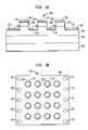
- FIG. 3Billustrates a top view of the Schottky diode 300 .
- the bond pad 312 and the underlying Schottky contactare located at the tops of the vertical mesas.
- the size of each mesais optimized to attain as a constant current density across the mesa as possible, thereby minimizing the forward operating voltage.
- circular mesasare shown arranged in a regular pattern, other geometric shapes and other pattern arrangements are also within the scope of the invention. Additionally, though FIG.
- the scope of the inventionalso includes configurations wherein the ohmic contact is only disposed between some or all of the mesas or only partially surrounds each of the mesas.
- solder bumps 320 or other interconnectsare formed atop each of the atop part of the bond pad metal 312 of the mesas. Additional interconnects, such as solder bumps 322 , may be provided at the edge of the bond pad metal 318 that is atop the ohmic contact or at other locations atop the layer 318 .
- FIG. 4illustrates a submount structure 400 according to another embodiment of the invention.
- the submount structureis suitable for mounting a Schottky diode, such as the arrangement shown in FIGS. 3A and 3B , in a flip chip arrangement.
- the submount structure 400includes a contact 410 which includes a contact region 420 to which some or all of the bond pad metal 312 atop the Schottky contacts are connected via interconnects, such as the solder bumps 320 .
- the contact 410also includes terminal regions 404 to provide connections external to the submount.
- Further contacts 412include contact regions 422 to which the bond pad 318 atop the ohmic contact is connected via further interconnects, such as the solder bumps 322 .
- Terminals 402are also provided for connections external to the submount.
- the flip chip assembly of the Schottky diode 300 and the submount 400reduces the spreading resistances of the Schottky and ohmic contacts, thereby further reducing the forward voltage drop in the device.
- solder bumps 322 or other interconnects shown in FIG. 3Bare located at the edge of the ohmic region, the invention also includes other arrangements.
- the solder bumps or other interconnects to the ohmic contactmay be located between some of the mesas.
- interconnectsare located between some of the mesas as well as at the edge of the device. The configuration of the contacts 400 and 420 is then arranged accordingly.
- FIG. 5illustrates such an alternative embodiment of the invention in which solder bumps 322 or other interconnects are located between some of the mesas as well as at the edge of the ohmic contact. Additionally, the external terminals are located at the bottom of the submount rather than at the top.
- the Schottky contactsare connected via the solder bumps 320 or other interconnects to contact regions 510 at the top surface of the submount substrate 502 .
- the contact regions 510are connected to a common contact 520 which is connected to a terminal 540 located at the bottom of the submount substrate by one or more vias 530 .
- the solder bumps 322 or other interconnectsconnect the ohmic contact of the Schottky diode to further contact regions 512 which are connected to a further common contact 522 .
- the further common contact 522is connected to an terminal 542 on the backside of the substrate by one or more further vias 532 .
- the provision of the terminals on the backside of the submount 500provides for an external connection that is isolated from the Schottky diode.
- an insulating passivation layer(not shown) may be deposited atop the Schottky diode prior to mounting on the substrate which electrically isolates the Schottky contact and its interconnect from the ohmic contact and its interconnect.
- portions of the top surface of the submountmay be raised to isolate the Schottky contact from the ohmic contact.
- the flip chip arrangements of the inventionhave the added advantage that when a thermally conductive submount material is used, such as silicon, aluminum nitride (AlN) or an electrically isolated metal, the submount also transports heat from the Schottky diode, thereby alleviating heat buildup at the thermally insulating substrate of the Schottky diode.
- a thermally conductive submount materialsuch as silicon, aluminum nitride (AlN) or an electrically isolated metal
- FIG. 6Aillustrates still another embodiment of the invention showing a Schottky diode 600 that is optimized to reduce the length of the conduction path as well as reduce the current spreading at the edge of the Schottky contact.
- a plurality of finger-shaped mesas 628intersect either with a central mesa 626 or with a bridge mesa 624 that, in turn, intersects with the central mesa 626 .
- One or more Schottky contactsare formed atop the finger-shaped mesas 628 , the bridge mesas 624 and the central mesa 626 .
- One or more ohmic contacts 632are formed between some or all of the finger shaped mesas 628 and reduce the current path between the Schottky contact and the ohmic contact.
- the central mesa 626may serve as a bonding pad region to an external submount, such as in the flip chip configuration described above.
- FIG. 6Billustrates a cross-sectional view of the Schottky diode shown in FIG. 6A taken along line B—B.
- a heavily doped layer 606is formed atop an insulating substrate 602 and atop an optional buffer region 604 in the manner described above with reference to FIG. 3A .
- a lower doped layer 608is formed as described above and is etched in a known manner to form the intersecting finger-shaped mesas 628 , the bridge mesas 624 and central mesa 626 shown in FIG. 6A .
- a Schottky contact 610is formed atop some or all of the mesas of lower doped layer, and a bond pad metal layer 612 is formed atop the Schottky contact 610 .
- One or more ohmic contacts 616are formed atop the lower doped layer 606 , and a bond pad metal 618 is formed atop the one or more ohmic contacts 616 .
- the ohmic contact 616 and bond pad metal 618are disposed between some or all the finger-shaped mesas 628 in an interdigitated manner to reduce the current path length.
- the Schottky contact 610 , the ohmic contact 616 and the bond pad metal 618may be comprised of the materials described above with reference to FIG. 3A .
- the dimensions of the finger-shaped mesas 628may be optimized for a given doping concentration and thickness of the lower doped layer 606 to reduce the current path length as well as reduce the current crowding effect at the edge of the Schottky contact, thereby reducing the forward resistance of the device.
- the length-to-width ratiois at least about 2:1 but is preferably from about 7:1 to about 10:1 when optimized as described above.
- the perimeter of the finger-shaped regionsmay be optimized to further optimize the current path length and current spreading.
- the perimeter of the combined structureis at least twice that of an imaginary rectangle 640 drawn around the structure but is preferably from about four to ten times that of the imaginary perimeter when similarly optimized. As a result, the forward resistance of the device is reduced.
Landscapes
- Engineering & Computer Science (AREA)
- Computer Hardware Design (AREA)
- Microelectronics & Electronic Packaging (AREA)
- Power Engineering (AREA)
- Electrodes Of Semiconductors (AREA)
Abstract
Description
Claims (77)
Priority Applications (9)
| Application Number | Priority Date | Filing Date | Title |
|---|---|---|---|
| US10/780,363US7084475B2 (en) | 2004-02-17 | 2004-02-17 | Lateral conduction Schottky diode with plural mesas |
| JP2005039132AJP5150803B2 (en) | 2004-02-17 | 2005-02-16 | Lateral conductivity Schottky diode with multiple mesas |
| TW094104495ATWI411008B (en) | 2004-02-17 | 2005-02-16 | Transverse conductive Schottky diode with a plurality of convex surfaces |
| TW101100217ATWI493597B (en) | 2004-02-17 | 2005-02-16 | Transverse conductive Schottky diode with a plurality of convex surfaces |
| CNB2005100075992ACN100517763C (en) | 2004-02-17 | 2005-02-17 | Lateral conduction Schottky diode with multiple mesas |
| FR0501625AFR2870046B1 (en) | 2004-02-17 | 2005-02-17 | SCHOTTKY DIODE WITH SATURATED LATERAL CONDUCTION |
| DE602005006025TDE602005006025T2 (en) | 2004-02-17 | 2005-02-17 | Lateral Schottky diode with several mesa |
| EP05290361AEP1564815B1 (en) | 2004-02-17 | 2005-02-17 | Lateral conduction schottky diode with plural mesas |
| AT05290361TATE392717T1 (en) | 2004-02-17 | 2005-02-17 | LATERAL SCHOTTKY DIODE WITH MULTIPLE MESA |
Applications Claiming Priority (1)
| Application Number | Priority Date | Filing Date | Title |
|---|---|---|---|
| US10/780,363US7084475B2 (en) | 2004-02-17 | 2004-02-17 | Lateral conduction Schottky diode with plural mesas |
Publications (2)
| Publication Number | Publication Date |
|---|---|
| US20050179104A1 US20050179104A1 (en) | 2005-08-18 |
| US7084475B2true US7084475B2 (en) | 2006-08-01 |
Family
ID=34701448
Family Applications (1)
| Application Number | Title | Priority Date | Filing Date |
|---|---|---|---|
| US10/780,363Expired - LifetimeUS7084475B2 (en) | 2004-02-17 | 2004-02-17 | Lateral conduction Schottky diode with plural mesas |
Country Status (8)
| Country | Link |
|---|---|
| US (1) | US7084475B2 (en) |
| EP (1) | EP1564815B1 (en) |
| JP (1) | JP5150803B2 (en) |
| CN (1) | CN100517763C (en) |
| AT (1) | ATE392717T1 (en) |
| DE (1) | DE602005006025T2 (en) |
| FR (1) | FR2870046B1 (en) |
| TW (2) | TWI411008B (en) |
Cited By (34)
| Publication number | Priority date | Publication date | Assignee | Title |
|---|---|---|---|---|
| US20100140660A1 (en)* | 2008-12-10 | 2010-06-10 | Yifeng Wu | Semiconductor Heterostructure Diodes |
| US20100207232A1 (en)* | 2009-02-18 | 2010-08-19 | Alpha & Omega Semiconductor, Inc. | Gallium Nitride Semiconductor Device With Improved Forward Conduction |
| US20110006307A1 (en)* | 2009-07-10 | 2011-01-13 | Tekcore Co., Ltd. | Group III-Nitride Semiconductor Schottky Diode and Its Fabrication Method |
| US20110101371A1 (en)* | 2005-01-06 | 2011-05-05 | Power Integrations, Inc. | Gallium nitride semiconductor |
| US20110121314A1 (en)* | 2007-09-17 | 2011-05-26 | Transphorm Inc. | Enhancement mode gallium nitride power devices |
| US8289065B2 (en) | 2008-09-23 | 2012-10-16 | Transphorm Inc. | Inductive load power switching circuits |
| US8390000B2 (en) | 2009-08-28 | 2013-03-05 | Transphorm Inc. | Semiconductor devices with field plates |
| US8390091B2 (en) | 2009-02-03 | 2013-03-05 | Freescale Semiconductor, Inc. | Semiconductor structure, an integrated circuit including a semiconductor structure and a method for manufacturing a semiconductor structure |
| US8389977B2 (en) | 2009-12-10 | 2013-03-05 | Transphorm Inc. | Reverse side engineered III-nitride devices |
| US8519438B2 (en) | 2008-04-23 | 2013-08-27 | Transphorm Inc. | Enhancement mode III-N HEMTs |
| US8598937B2 (en) | 2011-10-07 | 2013-12-03 | Transphorm Inc. | High power semiconductor electronic components with increased reliability |
| US8633094B2 (en) | 2011-12-01 | 2014-01-21 | Power Integrations, Inc. | GaN high voltage HFET with passivation plus gate dielectric multilayer structure |
| US8643062B2 (en) | 2011-02-02 | 2014-02-04 | Transphorm Inc. | III-N device structures and methods |
| US8716141B2 (en) | 2011-03-04 | 2014-05-06 | Transphorm Inc. | Electrode configurations for semiconductor devices |
| US8742460B2 (en) | 2010-12-15 | 2014-06-03 | Transphorm Inc. | Transistors with isolation regions |
| US8742459B2 (en) | 2009-05-14 | 2014-06-03 | Transphorm Inc. | High voltage III-nitride semiconductor devices |
| US8772842B2 (en) | 2011-03-04 | 2014-07-08 | Transphorm, Inc. | Semiconductor diodes with low reverse bias currents |
| US8901604B2 (en) | 2011-09-06 | 2014-12-02 | Transphorm Inc. | Semiconductor devices with guard rings |
| US8916929B2 (en) | 2004-06-10 | 2014-12-23 | Power Integrations, Inc. | MOSFET having a JFET embedded as a body diode |
| US8928037B2 (en) | 2013-02-28 | 2015-01-06 | Power Integrations, Inc. | Heterostructure power transistor with AlSiN passivation layer |
| US8940620B2 (en) | 2011-12-15 | 2015-01-27 | Power Integrations, Inc. | Composite wafer for fabrication of semiconductor devices |
| US9093366B2 (en) | 2012-04-09 | 2015-07-28 | Transphorm Inc. | N-polar III-nitride transistors |
| US9165766B2 (en) | 2012-02-03 | 2015-10-20 | Transphorm Inc. | Buffer layer structures suited for III-nitride devices with foreign substrates |
| US9171730B2 (en) | 2013-02-15 | 2015-10-27 | Transphorm Inc. | Electrodes for semiconductor devices and methods of forming the same |
| US9184275B2 (en) | 2012-06-27 | 2015-11-10 | Transphorm Inc. | Semiconductor devices with integrated hole collectors |
| US9245993B2 (en) | 2013-03-15 | 2016-01-26 | Transphorm Inc. | Carbon doping semiconductor devices |
| US9257547B2 (en) | 2011-09-13 | 2016-02-09 | Transphorm Inc. | III-N device structures having a non-insulating substrate |
| US9318593B2 (en) | 2014-07-21 | 2016-04-19 | Transphorm Inc. | Forming enhancement mode III-nitride devices |
| US9443938B2 (en) | 2013-07-19 | 2016-09-13 | Transphorm Inc. | III-nitride transistor including a p-type depleting layer |
| US9536967B2 (en) | 2014-12-16 | 2017-01-03 | Transphorm Inc. | Recessed ohmic contacts in a III-N device |
| US9536966B2 (en) | 2014-12-16 | 2017-01-03 | Transphorm Inc. | Gate structures for III-N devices |
| US9590060B2 (en) | 2013-03-13 | 2017-03-07 | Transphorm Inc. | Enhancement-mode III-nitride devices |
| US10224401B2 (en) | 2016-05-31 | 2019-03-05 | Transphorm Inc. | III-nitride devices including a graded depleting layer |
| US11322599B2 (en) | 2016-01-15 | 2022-05-03 | Transphorm Technology, Inc. | Enhancement mode III-nitride devices having an Al1-xSixO gate insulator |
Families Citing this family (11)
| Publication number | Priority date | Publication date | Assignee | Title |
|---|---|---|---|---|
| US20060151868A1 (en)* | 2005-01-10 | 2006-07-13 | Zhu Tinggang | Package for gallium nitride semiconductor devices |
| CN100385686C (en)* | 2005-08-30 | 2008-04-30 | 浙江大学 | A polycrystalline silicon germanium schottky diode and its preparation method |
| US8026568B2 (en)* | 2005-11-15 | 2011-09-27 | Velox Semiconductor Corporation | Second Schottky contact metal layer to improve GaN Schottky diode performance |
| KR101051578B1 (en)* | 2009-09-08 | 2011-07-22 | 삼성전기주식회사 | Semiconductor device and manufacturing method thereof |
| US8372738B2 (en)* | 2009-10-30 | 2013-02-12 | Alpha & Omega Semiconductor, Inc. | Method for manufacturing a gallium nitride based semiconductor device with improved termination scheme |
| JP5665361B2 (en)* | 2010-05-12 | 2015-02-04 | 三菱電機株式会社 | Silicon carbide semiconductor device and manufacturing method thereof |
| KR101193357B1 (en)* | 2010-12-09 | 2012-10-19 | 삼성전기주식회사 | Nitride based semiconductor device and method for manufacturing the same |
| US8872235B2 (en)* | 2012-02-23 | 2014-10-28 | Infineon Technologies Austria Ag | Integrated Schottky diode for HEMTs |
| JP5995234B2 (en)* | 2012-08-14 | 2016-09-21 | 株式会社レーザーシステム | Wireless connector for diode, power transmission system and power line |
| KR20150014641A (en)* | 2013-07-30 | 2015-02-09 | 서울반도체 주식회사 | Gallium nitnide based field effect transistor and method of fabricating the same |
| CN103400864B (en)* | 2013-07-31 | 2016-12-28 | 中国电子科技集团公司第十三研究所 | GaN transverse Schottky diode based on polarization doping |
Citations (22)
| Publication number | Priority date | Publication date | Assignee | Title |
|---|---|---|---|---|
| US3775200A (en) | 1970-08-29 | 1973-11-27 | Philips Corp | Schottky contact devices and method of manufacture |
| US4745445A (en) | 1983-03-15 | 1988-05-17 | Itt Gallium Arsenide Technology Center, A Division Of Itt Corporation | Interdigitated Schottky diode |
| US5602418A (en) | 1992-08-07 | 1997-02-11 | Asahi Kasei Kogyo Kabushiki Kaisha | Nitride based semiconductor device and manufacture thereof |
| US5877558A (en) | 1993-04-28 | 1999-03-02 | Nichia Chemical Industries, Ltd. | Gallium nitride-based III-V group compound semiconductor |
| US6184570B1 (en) | 1999-10-28 | 2001-02-06 | Ericsson Inc. | Integrated circuit dies including thermal stress reducing grooves and microelectronic packages utilizing the same |
| US20010034116A1 (en) | 2000-03-22 | 2001-10-25 | Lg Electronics Inc. | Semiconductor device with schottky contact and method for forming the same |
| US6331450B1 (en) | 1998-12-22 | 2001-12-18 | Toyoda Gosei Co., Ltd. | Method of manufacturing semiconductor device using group III nitride compound |
| US6344665B1 (en) | 2000-06-23 | 2002-02-05 | Arima Optoelectronics Corp. | Electrode structure of compound semiconductor device |
| US6380108B1 (en) | 1999-12-21 | 2002-04-30 | North Carolina State University | Pendeoepitaxial methods of fabricating gallium nitride semiconductor layers on weak posts, and gallium nitride semiconductor structures fabricated thereby |
| US6437374B1 (en) | 2001-05-07 | 2002-08-20 | Xerox Corporation | Semiconductor device and method of forming a semiconductor device |
| US20030015708A1 (en) | 2001-07-23 | 2003-01-23 | Primit Parikh | Gallium nitride based diodes with low forward voltage and low reverse current operation |
| US6524900B2 (en) | 2001-07-25 | 2003-02-25 | Abb Research, Ltd | Method concerning a junction barrier Schottky diode, such a diode and use thereof |
| US20030075728A1 (en) | 2001-10-18 | 2003-04-24 | Mitsubishi Denki Kabushiki Kaisha | Semiconductor device and method of manufacturing the same |
| US6573537B1 (en) | 1999-12-22 | 2003-06-03 | Lumileds Lighting, U.S., Llc | Highly reflective ohmic contacts to III-nitride flip-chip LEDs |
| US6586781B2 (en) | 2000-02-04 | 2003-07-01 | Cree Lighting Company | Group III nitride based FETs and HEMTs with reduced trapping and method for producing the same |
| US6586777B1 (en) | 1999-08-20 | 2003-07-01 | Sharp Kabushiki Kaisha | Nitride semiconductor light emitting device |
| US6593597B2 (en) | 2001-06-05 | 2003-07-15 | South Epitaxy Corporation | Group III-V element-based LED having ESD protection capacity |
| US6605854B2 (en) | 2001-02-01 | 2003-08-12 | Hitachi, Ltd. | Schottky diode with bump electrodes |
| US6608327B1 (en) | 1998-02-27 | 2003-08-19 | North Carolina State University | Gallium nitride semiconductor structure including laterally offset patterned layers |
| US6624444B1 (en)* | 2002-03-28 | 2003-09-23 | Intel Corporation | Electrical-optical package with capacitor DC shunts and associated methods |
| US6627967B2 (en)* | 2001-09-25 | 2003-09-30 | Sanyo Electric Co., Ltd. | Schottky barrier diode |
| US20050127465A1 (en)* | 2002-07-11 | 2005-06-16 | International Rectifier Corporation | Trench schottky barrier diode with differential oxide thickness |
Family Cites Families (12)
| Publication number | Priority date | Publication date | Assignee | Title |
|---|---|---|---|---|
| US4250520A (en)* | 1979-03-14 | 1981-02-10 | Rca Corporation | Flip chip mounted diode |
| JPS6022357A (en)* | 1983-07-18 | 1985-02-04 | Sumitomo Electric Ind Ltd | Schottky diode for level shift |
| JPH0332062A (en)* | 1989-06-29 | 1991-02-12 | Sharp Corp | Electrode structure and semiconductor element using the electrode structure |
| JPH08186083A (en)* | 1994-12-28 | 1996-07-16 | Hitachi Ltd | Method of forming metal film |
| US6891250B1 (en)* | 1999-04-30 | 2005-05-10 | Rohm Co., Ltd. | Semiconductor device with bipolar transistor |
| US6686616B1 (en)* | 2000-05-10 | 2004-02-03 | Cree, Inc. | Silicon carbide metal-semiconductor field effect transistors |
| US6682968B2 (en)* | 2000-07-27 | 2004-01-27 | Sanyo Electric Co., Ltd. | Manufacturing method of Schottky barrier diode |
| JP2003069048A (en)* | 2001-08-30 | 2003-03-07 | Sanyo Electric Co Ltd | Schottky barrier diode and method of manufacturing the same |
| JP2003023175A (en)* | 2001-07-10 | 2003-01-24 | Pawdec:Kk | Msm type semiconductor light receiving element |
| US20030034293A1 (en)* | 2001-08-16 | 2003-02-20 | Pti Advanced Filtration, Inc. | Method of treating filtration media to prevent lateral flow, blistering and de-lamination |
| KR200283621Y1 (en)* | 2002-03-18 | 2002-07-27 | (주)에스와이하이테크 | Voice Book Unit |
| KR101017657B1 (en)* | 2002-04-30 | 2011-02-25 | 크리 인코포레이티드 | High voltage switching device and manufacturing method thereof |
- 2004
- 2004-02-17USUS10/780,363patent/US7084475B2/ennot_activeExpired - Lifetime
- 2005
- 2005-02-16TWTW094104495Apatent/TWI411008B/ennot_activeIP Right Cessation
- 2005-02-16TWTW101100217Apatent/TWI493597B/ennot_activeIP Right Cessation
- 2005-02-16JPJP2005039132Apatent/JP5150803B2/ennot_activeExpired - Fee Related
- 2005-02-17DEDE602005006025Tpatent/DE602005006025T2/ennot_activeExpired - Lifetime
- 2005-02-17CNCNB2005100075992Apatent/CN100517763C/ennot_activeExpired - Fee Related
- 2005-02-17EPEP05290361Apatent/EP1564815B1/ennot_activeExpired - Lifetime
- 2005-02-17FRFR0501625Apatent/FR2870046B1/ennot_activeExpired - Fee Related
- 2005-02-17ATAT05290361Tpatent/ATE392717T1/ennot_activeIP Right Cessation
Patent Citations (25)
| Publication number | Priority date | Publication date | Assignee | Title |
|---|---|---|---|---|
| US3775200A (en) | 1970-08-29 | 1973-11-27 | Philips Corp | Schottky contact devices and method of manufacture |
| US4745445A (en) | 1983-03-15 | 1988-05-17 | Itt Gallium Arsenide Technology Center, A Division Of Itt Corporation | Interdigitated Schottky diode |
| US5602418A (en) | 1992-08-07 | 1997-02-11 | Asahi Kasei Kogyo Kabushiki Kaisha | Nitride based semiconductor device and manufacture thereof |
| US6507041B2 (en) | 1993-04-28 | 2003-01-14 | Nichia Chemical Industries, Ltd. | Gallium nitride-based III-V group compound semiconductor |
| US5877558A (en) | 1993-04-28 | 1999-03-02 | Nichia Chemical Industries, Ltd. | Gallium nitride-based III-V group compound semiconductor |
| US6610995B2 (en) | 1993-04-28 | 2003-08-26 | Nichia Corporation | Gallium nitride-based III-V group compound semiconductor |
| US6608327B1 (en) | 1998-02-27 | 2003-08-19 | North Carolina State University | Gallium nitride semiconductor structure including laterally offset patterned layers |
| US6331450B1 (en) | 1998-12-22 | 2001-12-18 | Toyoda Gosei Co., Ltd. | Method of manufacturing semiconductor device using group III nitride compound |
| US6586777B1 (en) | 1999-08-20 | 2003-07-01 | Sharp Kabushiki Kaisha | Nitride semiconductor light emitting device |
| US6184570B1 (en) | 1999-10-28 | 2001-02-06 | Ericsson Inc. | Integrated circuit dies including thermal stress reducing grooves and microelectronic packages utilizing the same |
| US6380108B1 (en) | 1999-12-21 | 2002-04-30 | North Carolina State University | Pendeoepitaxial methods of fabricating gallium nitride semiconductor layers on weak posts, and gallium nitride semiconductor structures fabricated thereby |
| US6573537B1 (en) | 1999-12-22 | 2003-06-03 | Lumileds Lighting, U.S., Llc | Highly reflective ohmic contacts to III-nitride flip-chip LEDs |
| US6586781B2 (en) | 2000-02-04 | 2003-07-01 | Cree Lighting Company | Group III nitride based FETs and HEMTs with reduced trapping and method for producing the same |
| US20010034116A1 (en) | 2000-03-22 | 2001-10-25 | Lg Electronics Inc. | Semiconductor device with schottky contact and method for forming the same |
| US6344665B1 (en) | 2000-06-23 | 2002-02-05 | Arima Optoelectronics Corp. | Electrode structure of compound semiconductor device |
| US6605854B2 (en) | 2001-02-01 | 2003-08-12 | Hitachi, Ltd. | Schottky diode with bump electrodes |
| US6437374B1 (en) | 2001-05-07 | 2002-08-20 | Xerox Corporation | Semiconductor device and method of forming a semiconductor device |
| US6593597B2 (en) | 2001-06-05 | 2003-07-15 | South Epitaxy Corporation | Group III-V element-based LED having ESD protection capacity |
| US20030062525A1 (en) | 2001-07-23 | 2003-04-03 | Cree Lighting Company | Gallium nitride based diodes with low forward voltage and low reverse current operation |
| US20030015708A1 (en) | 2001-07-23 | 2003-01-23 | Primit Parikh | Gallium nitride based diodes with low forward voltage and low reverse current operation |
| US6524900B2 (en) | 2001-07-25 | 2003-02-25 | Abb Research, Ltd | Method concerning a junction barrier Schottky diode, such a diode and use thereof |
| US6627967B2 (en)* | 2001-09-25 | 2003-09-30 | Sanyo Electric Co., Ltd. | Schottky barrier diode |
| US20030075728A1 (en) | 2001-10-18 | 2003-04-24 | Mitsubishi Denki Kabushiki Kaisha | Semiconductor device and method of manufacturing the same |
| US6624444B1 (en)* | 2002-03-28 | 2003-09-23 | Intel Corporation | Electrical-optical package with capacitor DC shunts and associated methods |
| US20050127465A1 (en)* | 2002-07-11 | 2005-06-16 | International Rectifier Corporation | Trench schottky barrier diode with differential oxide thickness |
Non-Patent Citations (1)
| Title |
|---|
| Yanagihara, et al., "Development of GaN-Based Electronic Device on Si", Sanken Technical Report, vol. 35, No. 1 (2003), pp. 11-14, Japan (English-language translation of Japanese-language publication). |
Cited By (85)
| Publication number | Priority date | Publication date | Assignee | Title |
|---|---|---|---|---|
| US8916929B2 (en) | 2004-06-10 | 2014-12-23 | Power Integrations, Inc. | MOSFET having a JFET embedded as a body diode |
| US20110101371A1 (en)* | 2005-01-06 | 2011-05-05 | Power Integrations, Inc. | Gallium nitride semiconductor |
| US9343560B2 (en) | 2007-09-17 | 2016-05-17 | Transphorm Inc. | Gallium nitride power devices |
| US8344424B2 (en) | 2007-09-17 | 2013-01-01 | Transphorm Inc. | Enhancement mode gallium nitride power devices |
| US20110121314A1 (en)* | 2007-09-17 | 2011-05-26 | Transphorm Inc. | Enhancement mode gallium nitride power devices |
| US8633518B2 (en) | 2007-09-17 | 2014-01-21 | Transphorm Inc. | Gallium nitride power devices |
| US8193562B2 (en) | 2007-09-17 | 2012-06-05 | Tansphorm Inc. | Enhancement mode gallium nitride power devices |
| US9196716B2 (en) | 2008-04-23 | 2015-11-24 | Transphorm Inc. | Enhancement mode III-N HEMTs |
| US8841702B2 (en) | 2008-04-23 | 2014-09-23 | Transphorm Inc. | Enhancement mode III-N HEMTs |
| US9437708B2 (en) | 2008-04-23 | 2016-09-06 | Transphorm Inc. | Enhancement mode III-N HEMTs |
| US8519438B2 (en) | 2008-04-23 | 2013-08-27 | Transphorm Inc. | Enhancement mode III-N HEMTs |
| US9941399B2 (en) | 2008-04-23 | 2018-04-10 | Transphorm Inc. | Enhancement mode III-N HEMTs |
| US8493129B2 (en) | 2008-09-23 | 2013-07-23 | Transphorm Inc. | Inductive load power switching circuits |
| US8531232B2 (en) | 2008-09-23 | 2013-09-10 | Transphorm Inc. | Inductive load power switching circuits |
| US8816751B2 (en) | 2008-09-23 | 2014-08-26 | Transphorm Inc. | Inductive load power switching circuits |
| US8289065B2 (en) | 2008-09-23 | 2012-10-16 | Transphorm Inc. | Inductive load power switching circuits |
| US9690314B2 (en) | 2008-09-23 | 2017-06-27 | Transphorm Inc. | Inductive load power switching circuits |
| CN102308390A (en)* | 2008-12-10 | 2012-01-04 | 特兰斯夫公司 | Semiconductor Heterostructure Diodes |
| US20100140660A1 (en)* | 2008-12-10 | 2010-06-10 | Yifeng Wu | Semiconductor Heterostructure Diodes |
| CN102308390B (en)* | 2008-12-10 | 2014-08-13 | 特兰斯夫公司 | Semiconductor Heterostructure Diodes |
| US7898004B2 (en) | 2008-12-10 | 2011-03-01 | Transphorm Inc. | Semiconductor heterostructure diodes |
| US8541818B2 (en) | 2008-12-10 | 2013-09-24 | Transphorm Inc. | Semiconductor heterostructure diodes |
| US8237198B2 (en) | 2008-12-10 | 2012-08-07 | Transphorm Inc. | Semiconductor heterostructure diodes |
| US9041065B2 (en) | 2008-12-10 | 2015-05-26 | Transphorm Inc. | Semiconductor heterostructure diodes |
| US8390091B2 (en) | 2009-02-03 | 2013-03-05 | Freescale Semiconductor, Inc. | Semiconductor structure, an integrated circuit including a semiconductor structure and a method for manufacturing a semiconductor structure |
| US8013414B2 (en) | 2009-02-18 | 2011-09-06 | Alpha & Omega Semiconductor, Inc. | Gallium nitride semiconductor device with improved forward conduction |
| US20120282762A1 (en)* | 2009-02-18 | 2012-11-08 | Alpha & Omega Semiconductor, Inc. | Method For Forming Gallium Nitride Semiconductor Device With Improved Forward Conduction |
| US20100207232A1 (en)* | 2009-02-18 | 2010-08-19 | Alpha & Omega Semiconductor, Inc. | Gallium Nitride Semiconductor Device With Improved Forward Conduction |
| US8253216B2 (en) | 2009-02-18 | 2012-08-28 | Alpha And Omega Semiconductor, Inc. | Gallium nitride semiconductor device with improved forward conduction |
| US8383499B2 (en)* | 2009-02-18 | 2013-02-26 | Alpha And Omega Semiconductor Incorporated | Method for forming gallium nitride semiconductor device with improved forward conduction |
| US9293561B2 (en) | 2009-05-14 | 2016-03-22 | Transphorm Inc. | High voltage III-nitride semiconductor devices |
| US8742459B2 (en) | 2009-05-14 | 2014-06-03 | Transphorm Inc. | High voltage III-nitride semiconductor devices |
| US20110006307A1 (en)* | 2009-07-10 | 2011-01-13 | Tekcore Co., Ltd. | Group III-Nitride Semiconductor Schottky Diode and Its Fabrication Method |
| US9111961B2 (en) | 2009-08-28 | 2015-08-18 | Transphorm Inc. | Semiconductor devices with field plates |
| US8390000B2 (en) | 2009-08-28 | 2013-03-05 | Transphorm Inc. | Semiconductor devices with field plates |
| US8692294B2 (en) | 2009-08-28 | 2014-04-08 | Transphorm Inc. | Semiconductor devices with field plates |
| US9831315B2 (en) | 2009-08-28 | 2017-11-28 | Transphorm Inc. | Semiconductor devices with field plates |
| US9373699B2 (en) | 2009-08-28 | 2016-06-21 | Transphorm Inc. | Semiconductor devices with field plates |
| US8389977B2 (en) | 2009-12-10 | 2013-03-05 | Transphorm Inc. | Reverse side engineered III-nitride devices |
| US9496137B2 (en) | 2009-12-10 | 2016-11-15 | Transphorm Inc. | Methods of forming reverse side engineered III-nitride devices |
| US10199217B2 (en) | 2009-12-10 | 2019-02-05 | Transphorm Inc. | Methods of forming reverse side engineered III-nitride devices |
| US9147760B2 (en) | 2010-12-15 | 2015-09-29 | Transphorm Inc. | Transistors with isolation regions |
| US9437707B2 (en) | 2010-12-15 | 2016-09-06 | Transphorm Inc. | Transistors with isolation regions |
| US8742460B2 (en) | 2010-12-15 | 2014-06-03 | Transphorm Inc. | Transistors with isolation regions |
| US8643062B2 (en) | 2011-02-02 | 2014-02-04 | Transphorm Inc. | III-N device structures and methods |
| US8895421B2 (en) | 2011-02-02 | 2014-11-25 | Transphorm Inc. | III-N device structures and methods |
| US9224671B2 (en) | 2011-02-02 | 2015-12-29 | Transphorm Inc. | III-N device structures and methods |
| US9142659B2 (en) | 2011-03-04 | 2015-09-22 | Transphorm Inc. | Electrode configurations for semiconductor devices |
| US8716141B2 (en) | 2011-03-04 | 2014-05-06 | Transphorm Inc. | Electrode configurations for semiconductor devices |
| US8895423B2 (en) | 2011-03-04 | 2014-11-25 | Transphorm Inc. | Method for making semiconductor diodes with low reverse bias currents |
| US8772842B2 (en) | 2011-03-04 | 2014-07-08 | Transphorm, Inc. | Semiconductor diodes with low reverse bias currents |
| US8901604B2 (en) | 2011-09-06 | 2014-12-02 | Transphorm Inc. | Semiconductor devices with guard rings |
| US9224805B2 (en) | 2011-09-06 | 2015-12-29 | Transphorm Inc. | Semiconductor devices with guard rings |
| US9257547B2 (en) | 2011-09-13 | 2016-02-09 | Transphorm Inc. | III-N device structures having a non-insulating substrate |
| US8860495B2 (en) | 2011-10-07 | 2014-10-14 | Transphorm Inc. | Method of forming electronic components with increased reliability |
| US8598937B2 (en) | 2011-10-07 | 2013-12-03 | Transphorm Inc. | High power semiconductor electronic components with increased reliability |
| US9171836B2 (en) | 2011-10-07 | 2015-10-27 | Transphorm Inc. | Method of forming electronic components with increased reliability |
| US8633094B2 (en) | 2011-12-01 | 2014-01-21 | Power Integrations, Inc. | GaN high voltage HFET with passivation plus gate dielectric multilayer structure |
| US8940620B2 (en) | 2011-12-15 | 2015-01-27 | Power Integrations, Inc. | Composite wafer for fabrication of semiconductor devices |
| US9165766B2 (en) | 2012-02-03 | 2015-10-20 | Transphorm Inc. | Buffer layer structures suited for III-nitride devices with foreign substrates |
| US9685323B2 (en) | 2012-02-03 | 2017-06-20 | Transphorm Inc. | Buffer layer structures suited for III-nitride devices with foreign substrates |
| US9490324B2 (en) | 2012-04-09 | 2016-11-08 | Transphorm Inc. | N-polar III-nitride transistors |
| US9093366B2 (en) | 2012-04-09 | 2015-07-28 | Transphorm Inc. | N-polar III-nitride transistors |
| US9634100B2 (en) | 2012-06-27 | 2017-04-25 | Transphorm Inc. | Semiconductor devices with integrated hole collectors |
| US9184275B2 (en) | 2012-06-27 | 2015-11-10 | Transphorm Inc. | Semiconductor devices with integrated hole collectors |
| US9520491B2 (en) | 2013-02-15 | 2016-12-13 | Transphorm Inc. | Electrodes for semiconductor devices and methods of forming the same |
| US9171730B2 (en) | 2013-02-15 | 2015-10-27 | Transphorm Inc. | Electrodes for semiconductor devices and methods of forming the same |
| US8928037B2 (en) | 2013-02-28 | 2015-01-06 | Power Integrations, Inc. | Heterostructure power transistor with AlSiN passivation layer |
| US10043898B2 (en) | 2013-03-13 | 2018-08-07 | Transphorm Inc. | Enhancement-mode III-nitride devices |
| US9590060B2 (en) | 2013-03-13 | 2017-03-07 | Transphorm Inc. | Enhancement-mode III-nitride devices |
| US10535763B2 (en) | 2013-03-13 | 2020-01-14 | Transphorm Inc. | Enhancement-mode III-nitride devices |
| US9245993B2 (en) | 2013-03-15 | 2016-01-26 | Transphorm Inc. | Carbon doping semiconductor devices |
| US9865719B2 (en) | 2013-03-15 | 2018-01-09 | Transphorm Inc. | Carbon doping semiconductor devices |
| US9245992B2 (en) | 2013-03-15 | 2016-01-26 | Transphorm Inc. | Carbon doping semiconductor devices |
| US10043896B2 (en) | 2013-07-19 | 2018-08-07 | Transphorm Inc. | III-Nitride transistor including a III-N depleting layer |
| US9842922B2 (en) | 2013-07-19 | 2017-12-12 | Transphorm Inc. | III-nitride transistor including a p-type depleting layer |
| US9443938B2 (en) | 2013-07-19 | 2016-09-13 | Transphorm Inc. | III-nitride transistor including a p-type depleting layer |
| US9935190B2 (en) | 2014-07-21 | 2018-04-03 | Transphorm Inc. | Forming enhancement mode III-nitride devices |
| US9318593B2 (en) | 2014-07-21 | 2016-04-19 | Transphorm Inc. | Forming enhancement mode III-nitride devices |
| US9536966B2 (en) | 2014-12-16 | 2017-01-03 | Transphorm Inc. | Gate structures for III-N devices |
| US9536967B2 (en) | 2014-12-16 | 2017-01-03 | Transphorm Inc. | Recessed ohmic contacts in a III-N device |
| US11322599B2 (en) | 2016-01-15 | 2022-05-03 | Transphorm Technology, Inc. | Enhancement mode III-nitride devices having an Al1-xSixO gate insulator |
| US10224401B2 (en) | 2016-05-31 | 2019-03-05 | Transphorm Inc. | III-nitride devices including a graded depleting layer |
| US10629681B2 (en) | 2016-05-31 | 2020-04-21 | Transphorm Technology, Inc. | III-nitride devices including a graded depleting layer |
| US11121216B2 (en) | 2016-05-31 | 2021-09-14 | Transphorm Technology, Inc. | III-nitride devices including a graded depleting layer |
Also Published As
| Publication number | Publication date |
|---|---|
| US20050179104A1 (en) | 2005-08-18 |
| EP1564815A1 (en) | 2005-08-17 |
| TWI411008B (en) | 2013-10-01 |
| FR2870046A1 (en) | 2005-11-11 |
| TW200601396A (en) | 2006-01-01 |
| EP1564815B1 (en) | 2008-04-16 |
| ATE392717T1 (en) | 2008-05-15 |
| CN1658402A (en) | 2005-08-24 |
| DE602005006025D1 (en) | 2008-05-29 |
| CN100517763C (en) | 2009-07-22 |
| TWI493597B (en) | 2015-07-21 |
| TW201230143A (en) | 2012-07-16 |
| FR2870046B1 (en) | 2008-01-18 |
| DE602005006025T2 (en) | 2009-05-07 |
| JP5150803B2 (en) | 2013-02-27 |
| JP2005236288A (en) | 2005-09-02 |
Similar Documents
| Publication | Publication Date | Title |
|---|---|---|
| US7084475B2 (en) | Lateral conduction Schottky diode with plural mesas | |
| US10573762B2 (en) | Vertical gallium nitride Schottky diode | |
| US8629525B2 (en) | Second contact schottky metal layer to improve GaN schottky diode performance | |
| US8927402B2 (en) | Method for forming termination structure for gallium nitride Schottky diode | |
| JP5240966B2 (en) | Gallium nitride semiconductor device | |
| US8253216B2 (en) | Gallium nitride semiconductor device with improved forward conduction | |
| JP2007305954A (en) | Field effect transistor and device thereof | |
| JP5150802B2 (en) | Low doped layers for nitride based semiconductor devices |
Legal Events
| Date | Code | Title | Description |
|---|---|---|---|
| AS | Assignment | Owner name:EMCORE CORPORATION, NEW JERSEY Free format text:ASSIGNMENT OF ASSIGNORS INTEREST;ASSIGNORS:SHELTON, BRYAN S.;LIU, LINLIN;CERUZZI, ALEX D.;AND OTHERS;REEL/FRAME:015004/0522;SIGNING DATES FROM 20040104 TO 20040119 | |
| AS | Assignment | Owner name:VELOX SEMICONDUCTOR CORPORATION, NEW JERSEY Free format text:ASSIGNMENT OF ASSIGNORS INTEREST;ASSIGNOR:EMCORE CORPORATION;REEL/FRAME:017397/0600 Effective date:20050429 | |
| AS | Assignment | Owner name:VELOX SEMICONDUCTOR CORPORATION, NEW JERSEY Free format text:ASSIGNMENT OF ASSIGNORS INTEREST;ASSIGNOR:EMCORE CORPORATION;REEL/FRAME:017508/0336 Effective date:20051010 | |
| STCF | Information on status: patent grant | Free format text:PATENTED CASE | |
| FEPP | Fee payment procedure | Free format text:PAT HOLDER NO LONGER CLAIMS SMALL ENTITY STATUS, ENTITY STATUS SET TO UNDISCOUNTED (ORIGINAL EVENT CODE: STOL); ENTITY STATUS OF PATENT OWNER: LARGE ENTITY | |
| FPAY | Fee payment | Year of fee payment:4 | |
| AS | Assignment | Owner name:POWER INTEGRATIONS, INC., CALIFORNIA Free format text:ASSIGNMENT OF ASSIGNORS INTEREST;ASSIGNOR:VELOX SEMICONDUCTOR CORPORATION;REEL/FRAME:024927/0893 Effective date:20100826 | |
| FPAY | Fee payment | Year of fee payment:8 | |
| FEPP | Fee payment procedure | Free format text:11.5 YR SURCHARGE- LATE PMT W/IN 6 MO, LARGE ENTITY (ORIGINAL EVENT CODE: M1556) | |
| MAFP | Maintenance fee payment | Free format text:PAYMENT OF MAINTENANCE FEE, 12TH YEAR, LARGE ENTITY (ORIGINAL EVENT CODE: M1553) Year of fee payment:12 |