US7084078B2 - Atomic layer deposited lanthanide doped TiOx dielectric films - Google Patents
Atomic layer deposited lanthanide doped TiOx dielectric filmsDownload PDFInfo
- Publication number
- US7084078B2 US7084078B2US10/233,309US23330902AUS7084078B2US 7084078 B2US7084078 B2US 7084078B2US 23330902 AUS23330902 AUS 23330902AUS 7084078 B2US7084078 B2US 7084078B2
- Authority
- US
- United States
- Prior art keywords
- lanthanide
- titanium
- pulsing
- dopant
- precursor
- Prior art date
- Legal status (The legal status is an assumption and is not a legal conclusion. Google has not performed a legal analysis and makes no representation as to the accuracy of the status listed.)
- Expired - Fee Related
Links
Images


Classifications
- H—ELECTRICITY
- H01—ELECTRIC ELEMENTS
- H01L—SEMICONDUCTOR DEVICES NOT COVERED BY CLASS H10
- H01L21/00—Processes or apparatus adapted for the manufacture or treatment of semiconductor or solid state devices or of parts thereof
- H01L21/02—Manufacture or treatment of semiconductor devices or of parts thereof
- H01L21/02104—Forming layers
- H01L21/02107—Forming insulating materials on a substrate
- H01L21/02109—Forming insulating materials on a substrate characterised by the type of layer, e.g. type of material, porous/non-porous, pre-cursors, mixtures or laminates
- H01L21/02112—Forming insulating materials on a substrate characterised by the type of layer, e.g. type of material, porous/non-porous, pre-cursors, mixtures or laminates characterised by the material of the layer
- H01L21/02172—Forming insulating materials on a substrate characterised by the type of layer, e.g. type of material, porous/non-porous, pre-cursors, mixtures or laminates characterised by the material of the layer the material containing at least one metal element, e.g. metal oxides, metal nitrides, metal oxynitrides or metal carbides
- H01L21/02175—Forming insulating materials on a substrate characterised by the type of layer, e.g. type of material, porous/non-porous, pre-cursors, mixtures or laminates characterised by the material of the layer the material containing at least one metal element, e.g. metal oxides, metal nitrides, metal oxynitrides or metal carbides characterised by the metal
- H01L21/02194—Forming insulating materials on a substrate characterised by the type of layer, e.g. type of material, porous/non-porous, pre-cursors, mixtures or laminates characterised by the material of the layer the material containing at least one metal element, e.g. metal oxides, metal nitrides, metal oxynitrides or metal carbides characterised by the metal the material containing more than one metal element
- C—CHEMISTRY; METALLURGY
- C23—COATING METALLIC MATERIAL; COATING MATERIAL WITH METALLIC MATERIAL; CHEMICAL SURFACE TREATMENT; DIFFUSION TREATMENT OF METALLIC MATERIAL; COATING BY VACUUM EVAPORATION, BY SPUTTERING, BY ION IMPLANTATION OR BY CHEMICAL VAPOUR DEPOSITION, IN GENERAL; INHIBITING CORROSION OF METALLIC MATERIAL OR INCRUSTATION IN GENERAL
- C23C—COATING METALLIC MATERIAL; COATING MATERIAL WITH METALLIC MATERIAL; SURFACE TREATMENT OF METALLIC MATERIAL BY DIFFUSION INTO THE SURFACE, BY CHEMICAL CONVERSION OR SUBSTITUTION; COATING BY VACUUM EVAPORATION, BY SPUTTERING, BY ION IMPLANTATION OR BY CHEMICAL VAPOUR DEPOSITION, IN GENERAL
- C23C16/00—Chemical coating by decomposition of gaseous compounds, without leaving reaction products of surface material in the coating, i.e. chemical vapour deposition [CVD] processes
- C23C16/22—Chemical coating by decomposition of gaseous compounds, without leaving reaction products of surface material in the coating, i.e. chemical vapour deposition [CVD] processes characterised by the deposition of inorganic material, other than metallic material
- C23C16/30—Deposition of compounds, mixtures or solid solutions, e.g. borides, carbides, nitrides
- C23C16/40—Oxides
- C23C16/405—Oxides of refractory metals or yttrium
- C—CHEMISTRY; METALLURGY
- C23—COATING METALLIC MATERIAL; COATING MATERIAL WITH METALLIC MATERIAL; CHEMICAL SURFACE TREATMENT; DIFFUSION TREATMENT OF METALLIC MATERIAL; COATING BY VACUUM EVAPORATION, BY SPUTTERING, BY ION IMPLANTATION OR BY CHEMICAL VAPOUR DEPOSITION, IN GENERAL; INHIBITING CORROSION OF METALLIC MATERIAL OR INCRUSTATION IN GENERAL
- C23C—COATING METALLIC MATERIAL; COATING MATERIAL WITH METALLIC MATERIAL; SURFACE TREATMENT OF METALLIC MATERIAL BY DIFFUSION INTO THE SURFACE, BY CHEMICAL CONVERSION OR SUBSTITUTION; COATING BY VACUUM EVAPORATION, BY SPUTTERING, BY ION IMPLANTATION OR BY CHEMICAL VAPOUR DEPOSITION, IN GENERAL
- C23C16/00—Chemical coating by decomposition of gaseous compounds, without leaving reaction products of surface material in the coating, i.e. chemical vapour deposition [CVD] processes
- C23C16/44—Chemical coating by decomposition of gaseous compounds, without leaving reaction products of surface material in the coating, i.e. chemical vapour deposition [CVD] processes characterised by the method of coating
- C23C16/455—Chemical coating by decomposition of gaseous compounds, without leaving reaction products of surface material in the coating, i.e. chemical vapour deposition [CVD] processes characterised by the method of coating characterised by the method used for introducing gases into reaction chamber or for modifying gas flows in reaction chamber
- C23C16/45523—Pulsed gas flow or change of composition over time
- C23C16/45525—Atomic layer deposition [ALD]
- C23C16/45527—Atomic layer deposition [ALD] characterized by the ALD cycle, e.g. different flows or temperatures during half-reactions, unusual pulsing sequence, use of precursor mixtures or auxiliary reactants or activations
- C23C16/45531—Atomic layer deposition [ALD] characterized by the ALD cycle, e.g. different flows or temperatures during half-reactions, unusual pulsing sequence, use of precursor mixtures or auxiliary reactants or activations specially adapted for making ternary or higher compositions
- H—ELECTRICITY
- H01—ELECTRIC ELEMENTS
- H01L—SEMICONDUCTOR DEVICES NOT COVERED BY CLASS H10
- H01L21/00—Processes or apparatus adapted for the manufacture or treatment of semiconductor or solid state devices or of parts thereof
- H01L21/02—Manufacture or treatment of semiconductor devices or of parts thereof
- H01L21/02104—Forming layers
- H01L21/02107—Forming insulating materials on a substrate
- H01L21/02109—Forming insulating materials on a substrate characterised by the type of layer, e.g. type of material, porous/non-porous, pre-cursors, mixtures or laminates
- H01L21/02112—Forming insulating materials on a substrate characterised by the type of layer, e.g. type of material, porous/non-porous, pre-cursors, mixtures or laminates characterised by the material of the layer
- H01L21/02172—Forming insulating materials on a substrate characterised by the type of layer, e.g. type of material, porous/non-porous, pre-cursors, mixtures or laminates characterised by the material of the layer the material containing at least one metal element, e.g. metal oxides, metal nitrides, metal oxynitrides or metal carbides
- H01L21/02175—Forming insulating materials on a substrate characterised by the type of layer, e.g. type of material, porous/non-porous, pre-cursors, mixtures or laminates characterised by the material of the layer the material containing at least one metal element, e.g. metal oxides, metal nitrides, metal oxynitrides or metal carbides characterised by the metal
- H01L21/02186—Forming insulating materials on a substrate characterised by the type of layer, e.g. type of material, porous/non-porous, pre-cursors, mixtures or laminates characterised by the material of the layer the material containing at least one metal element, e.g. metal oxides, metal nitrides, metal oxynitrides or metal carbides characterised by the metal the material containing titanium, e.g. TiO2
- H—ELECTRICITY
- H01—ELECTRIC ELEMENTS
- H01L—SEMICONDUCTOR DEVICES NOT COVERED BY CLASS H10
- H01L21/00—Processes or apparatus adapted for the manufacture or treatment of semiconductor or solid state devices or of parts thereof
- H01L21/02—Manufacture or treatment of semiconductor devices or of parts thereof
- H01L21/04—Manufacture or treatment of semiconductor devices or of parts thereof the devices having potential barriers, e.g. a PN junction, depletion layer or carrier concentration layer
- H01L21/18—Manufacture or treatment of semiconductor devices or of parts thereof the devices having potential barriers, e.g. a PN junction, depletion layer or carrier concentration layer the devices having semiconductor bodies comprising elements of Group IV of the Periodic Table or AIIIBV compounds with or without impurities, e.g. doping materials
- H01L21/28—Manufacture of electrodes on semiconductor bodies using processes or apparatus not provided for in groups H01L21/20 - H01L21/268
- H01L21/28008—Making conductor-insulator-semiconductor electrodes
- H01L21/28017—Making conductor-insulator-semiconductor electrodes the insulator being formed after the semiconductor body, the semiconductor being silicon
- H01L21/28158—Making the insulator
- H01L21/28167—Making the insulator on single crystalline silicon, e.g. using a liquid, i.e. chemical oxidation
- H01L21/28185—Making the insulator on single crystalline silicon, e.g. using a liquid, i.e. chemical oxidation with a treatment, e.g. annealing, after the formation of the gate insulator and before the formation of the definitive gate conductor
- H—ELECTRICITY
- H01—ELECTRIC ELEMENTS
- H01L—SEMICONDUCTOR DEVICES NOT COVERED BY CLASS H10
- H01L21/00—Processes or apparatus adapted for the manufacture or treatment of semiconductor or solid state devices or of parts thereof
- H01L21/02—Manufacture or treatment of semiconductor devices or of parts thereof
- H01L21/04—Manufacture or treatment of semiconductor devices or of parts thereof the devices having potential barriers, e.g. a PN junction, depletion layer or carrier concentration layer
- H01L21/18—Manufacture or treatment of semiconductor devices or of parts thereof the devices having potential barriers, e.g. a PN junction, depletion layer or carrier concentration layer the devices having semiconductor bodies comprising elements of Group IV of the Periodic Table or AIIIBV compounds with or without impurities, e.g. doping materials
- H01L21/28—Manufacture of electrodes on semiconductor bodies using processes or apparatus not provided for in groups H01L21/20 - H01L21/268
- H01L21/28008—Making conductor-insulator-semiconductor electrodes
- H01L21/28017—Making conductor-insulator-semiconductor electrodes the insulator being formed after the semiconductor body, the semiconductor being silicon
- H01L21/28158—Making the insulator
- H01L21/28167—Making the insulator on single crystalline silicon, e.g. using a liquid, i.e. chemical oxidation
- H01L21/28194—Making the insulator on single crystalline silicon, e.g. using a liquid, i.e. chemical oxidation by deposition, e.g. evaporation, ALD, CVD, sputtering, laser deposition
- H—ELECTRICITY
- H10—SEMICONDUCTOR DEVICES; ELECTRIC SOLID-STATE DEVICES NOT OTHERWISE PROVIDED FOR
- H10D—INORGANIC ELECTRIC SEMICONDUCTOR DEVICES
- H10D64/00—Electrodes of devices having potential barriers
- H10D64/60—Electrodes characterised by their materials
- H10D64/66—Electrodes having a conductor capacitively coupled to a semiconductor by an insulator, e.g. MIS electrodes
- H10D64/68—Electrodes having a conductor capacitively coupled to a semiconductor by an insulator, e.g. MIS electrodes characterised by the insulator, e.g. by the gate insulator
- H10D64/681—Electrodes having a conductor capacitively coupled to a semiconductor by an insulator, e.g. MIS electrodes characterised by the insulator, e.g. by the gate insulator having a compositional variation, e.g. multilayered
- H10D64/685—Electrodes having a conductor capacitively coupled to a semiconductor by an insulator, e.g. MIS electrodes characterised by the insulator, e.g. by the gate insulator having a compositional variation, e.g. multilayered being perpendicular to the channel plane
- H—ELECTRICITY
- H10—SEMICONDUCTOR DEVICES; ELECTRIC SOLID-STATE DEVICES NOT OTHERWISE PROVIDED FOR
- H10D—INORGANIC ELECTRIC SEMICONDUCTOR DEVICES
- H10D64/00—Electrodes of devices having potential barriers
- H10D64/60—Electrodes characterised by their materials
- H10D64/66—Electrodes having a conductor capacitively coupled to a semiconductor by an insulator, e.g. MIS electrodes
- H10D64/68—Electrodes having a conductor capacitively coupled to a semiconductor by an insulator, e.g. MIS electrodes characterised by the insulator, e.g. by the gate insulator
- H10D64/691—Electrodes having a conductor capacitively coupled to a semiconductor by an insulator, e.g. MIS electrodes characterised by the insulator, e.g. by the gate insulator comprising metallic compounds, e.g. metal oxides or metal silicates
- H—ELECTRICITY
- H01—ELECTRIC ELEMENTS
- H01L—SEMICONDUCTOR DEVICES NOT COVERED BY CLASS H10
- H01L21/00—Processes or apparatus adapted for the manufacture or treatment of semiconductor or solid state devices or of parts thereof
- H01L21/02—Manufacture or treatment of semiconductor devices or of parts thereof
- H01L21/02104—Forming layers
- H01L21/02107—Forming insulating materials on a substrate
- H01L21/02109—Forming insulating materials on a substrate characterised by the type of layer, e.g. type of material, porous/non-porous, pre-cursors, mixtures or laminates
- H01L21/02112—Forming insulating materials on a substrate characterised by the type of layer, e.g. type of material, porous/non-porous, pre-cursors, mixtures or laminates characterised by the material of the layer
- H01L21/02172—Forming insulating materials on a substrate characterised by the type of layer, e.g. type of material, porous/non-porous, pre-cursors, mixtures or laminates characterised by the material of the layer the material containing at least one metal element, e.g. metal oxides, metal nitrides, metal oxynitrides or metal carbides
- H01L21/02175—Forming insulating materials on a substrate characterised by the type of layer, e.g. type of material, porous/non-porous, pre-cursors, mixtures or laminates characterised by the material of the layer the material containing at least one metal element, e.g. metal oxides, metal nitrides, metal oxynitrides or metal carbides characterised by the metal
- H01L21/02192—Forming insulating materials on a substrate characterised by the type of layer, e.g. type of material, porous/non-porous, pre-cursors, mixtures or laminates characterised by the material of the layer the material containing at least one metal element, e.g. metal oxides, metal nitrides, metal oxynitrides or metal carbides characterised by the metal the material containing at least one rare earth metal element, e.g. oxides of lanthanides, scandium or yttrium
- H—ELECTRICITY
- H01—ELECTRIC ELEMENTS
- H01L—SEMICONDUCTOR DEVICES NOT COVERED BY CLASS H10
- H01L21/00—Processes or apparatus adapted for the manufacture or treatment of semiconductor or solid state devices or of parts thereof
- H01L21/02—Manufacture or treatment of semiconductor devices or of parts thereof
- H01L21/02104—Forming layers
- H01L21/02107—Forming insulating materials on a substrate
- H01L21/02225—Forming insulating materials on a substrate characterised by the process for the formation of the insulating layer
- H01L21/0226—Forming insulating materials on a substrate characterised by the process for the formation of the insulating layer formation by a deposition process
- H01L21/02263—Forming insulating materials on a substrate characterised by the process for the formation of the insulating layer formation by a deposition process deposition from the gas or vapour phase
- H01L21/02271—Forming insulating materials on a substrate characterised by the process for the formation of the insulating layer formation by a deposition process deposition from the gas or vapour phase deposition by decomposition or reaction of gaseous or vapour phase compounds, i.e. chemical vapour deposition
- H01L21/0228—Forming insulating materials on a substrate characterised by the process for the formation of the insulating layer formation by a deposition process deposition from the gas or vapour phase deposition by decomposition or reaction of gaseous or vapour phase compounds, i.e. chemical vapour deposition deposition by cyclic CVD, e.g. ALD, ALE, pulsed CVD
- H—ELECTRICITY
- H01—ELECTRIC ELEMENTS
- H01L—SEMICONDUCTOR DEVICES NOT COVERED BY CLASS H10
- H01L21/00—Processes or apparatus adapted for the manufacture or treatment of semiconductor or solid state devices or of parts thereof
- H01L21/02—Manufacture or treatment of semiconductor devices or of parts thereof
- H01L21/04—Manufacture or treatment of semiconductor devices or of parts thereof the devices having potential barriers, e.g. a PN junction, depletion layer or carrier concentration layer
- H01L21/18—Manufacture or treatment of semiconductor devices or of parts thereof the devices having potential barriers, e.g. a PN junction, depletion layer or carrier concentration layer the devices having semiconductor bodies comprising elements of Group IV of the Periodic Table or AIIIBV compounds with or without impurities, e.g. doping materials
- H01L21/30—Treatment of semiconductor bodies using processes or apparatus not provided for in groups H01L21/20 - H01L21/26
- H01L21/31—Treatment of semiconductor bodies using processes or apparatus not provided for in groups H01L21/20 - H01L21/26 to form insulating layers thereon, e.g. for masking or by using photolithographic techniques; After treatment of these layers; Selection of materials for these layers
- H01L21/3105—After-treatment
- H01L21/3115—Doping the insulating layers
- H—ELECTRICITY
- H10—SEMICONDUCTOR DEVICES; ELECTRIC SOLID-STATE DEVICES NOT OTHERWISE PROVIDED FOR
- H10D—INORGANIC ELECTRIC SEMICONDUCTOR DEVICES
- H10D64/00—Electrodes of devices having potential barriers
- H10D64/60—Electrodes characterised by their materials
- H10D64/66—Electrodes having a conductor capacitively coupled to a semiconductor by an insulator, e.g. MIS electrodes
- H10D64/68—Electrodes having a conductor capacitively coupled to a semiconductor by an insulator, e.g. MIS electrodes characterised by the insulator, e.g. by the gate insulator
- H10D64/693—Electrodes having a conductor capacitively coupled to a semiconductor by an insulator, e.g. MIS electrodes characterised by the insulator, e.g. by the gate insulator the insulator comprising nitrogen, e.g. nitrides, oxynitrides or nitrogen-doped materials
Definitions
- the inventionrelates to semiconductor devices and device fabrication. Specifically, the invention relates to gate dielectric layers and their method of fabrication.
- the semiconductor device industryhas a market driven need to improve speed performance, improve its low static (off-state) power requirements, and adapt to a wide range of power supply and output voltage requirements for it silicon based microelectronic products.
- transistorsthere is continuous pressure to reduce the size of devices such as transistors.
- the ultimate goalis to fabricate increasingly smaller and more reliable integrated circuits (ICs) for use in products such as processor chips, mobile telephones, and memory devices such as dynamic random access memories (DRAMs).
- ICsintegrated circuits
- DRAMsdynamic random access memories
- the smaller devicesare frequently powered by batteries, where there is also pressure to reduce the size of the batteries, and to extend the time between battery charges. This forces the industry to not only design smaller transistors, but to design them to operate reliably with lower power supplies.
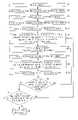
- FIG. 1A common configuration of such a transistor is shown in FIG. 1 . While the following discussion uses FIG. 1 to illustrate a transistor from the prior art, one skilled in the art will recognize that the present invention could be incorporated into the transistor shown in FIG. 1 to form a novel transistor according to the invention.
- a transistor 100is fabricated in a substrate 110 that is typically silicon, but could be fabricated from other semiconductor materials as well. Transistor 100 has a source region 120 and a drain region 130 .
- a body region 132is located between source region 120 and drain region 130 , where body region 132 defines a channel of the transistor with a channel length 134 .
- a gate dielectric 140is located on body region 132 with a gate 150 located over gate dielectric 140 .
- gate dielectric 140can be formed from materials other than oxides, gate dielectric 140 is typically an oxide, and is commonly referred to as a gate oxide.
- Gate 150may be fabricated from polycrystalline silicon (polysilicon), or other conducting materials such as metal may be used.
- gate dielectric 140In fabricating transistors to be smaller in size and reliably operate on lower power supplies, one important design criteria is gate dielectric 140 .
- the mainstay for forming the gate dielectrichas been silicon dioxide, SiO 2 .
- a thermally grown amorphous SiO 2 layerprovides an electrically and thermodynamically stable material, where the interface of the SiO 2 layer with underlying Si provides a high quality interface as well as superior electrical isolation properties.
- use of SiO 2 on Sihas provided defect charge densities on the order of 10 10 /cm 2 , midgap interface state densities of approximately 10 10 /cm 2 eV, and breakdown voltages in the range of 15 MV/cm. With such qualities, there would be no apparent need to use a material other than SiO 2 , but increased scaling and other requirements for gate dielectrics create the need to find other dielectric materials to be used for a gate dielectric.
- a method of forming a dielectric filmincludes the formation of lanthanide doped TiO x by atomic layer deposition (ALD).
- ALD formation of the lanthanide doped TiO x layerincludes depositing titanium and oxygen onto a substrate surface by atomic layer deposition, and depositing a lanthanide dopant by atomic layer deposition onto the substrate surface containing the deposited titanium and oxygen.
- the dopantis selected from a group consisting of Nd, Tb, and Dy.
- the lanthanide doped TiO x layer thicknessis controlled by processing a total number of ALD cycles to produce the desired thickness.
- a dielectric film containing lanthanide doped TiO xhas a larger dielectric constant than silicon dioxide, a relatively small leakage current, and good stability with respect to a silicon based substrate.
- Embodimentsinclude forming capacitors, transistors, memory devices, and electronic systems having dielectric layers containing atomic layer deposited lanthanide doped TiO x .
- dielectric filmscontaining atomic layer deposited lanthanide doped TiO x .
- Such dielectric filmsprovide a significantly thinner equivalent oxide thickness compared with a silicon oxide layer having the same physical thickness.
- dielectric filmsprovide a significantly thicker physical thickness than a silicon oxide layer having the same equivalent oxide thickness.
- FIG. 1shows a common configuration of a transistor in which an embodiment of a gate dielectric containing atomic layer deposited lanthanide doped TiO x can be formed according to the teachings of the present invention.
- FIG. 2Ashows an embodiment of an atomic layer deposition system for processing a dielectric film containing lanthanide doped TiO x , according to the teachings of the present invention.
- FIG. 2Bshows an embodiment of a gas-distribution fixture of an atomic layer deposition system for processing a dielectric film containing lanthanide doped TiO x , according to the teachings of the present invention.
- FIGS. 3A–3Billustrate flow diagrams of elements for an embodiment of a method to process a dielectric film containing lanthanide doped TiO x by atomic layer deposition, according to the teachings of the present invention.
- FIG. 4Aillustrates a flow diagram of elements for another embodiment of a method to process a dielectric film containing TiO x doped with a lanthanide by atomic layer deposition, according to the teachings of the present invention.
- FIG. 4Billustrates a flow diagram of elements for another embodiment of a method for doping TiO x with a lanthanide to form a dielectric film by atomic layer deposition, according to the teachings of the present invention.
- FIG. 5shows an embodiment of a configuration of a transistor having an atomic layer deposited lanthanide doped TiO x dielectric film, according to the teachings of the present invention.
- FIG. 6shows an embodiment of a personal computer incorporating devices having an atomic layer deposited lanthanide doped TiO x dielectric film, according to the teachings of the present invention.
- FIG. 7illustrates a schematic view of an embodiment of a central processing unit incorporating devices having an atomic layer deposited lanthanide doped TiO x dielectric film, according to the teachings of the present invention.
- FIG. 8illustrates a schematic view of an embodiment of a DRAM memory device having an atomic layer deposited lanthanide doped TiO x dielectric film, according to the teachings of the present invention.
- wafer and substrate used in the following descriptioninclude any structure having an exposed surface with which to form the integrated circuit (IC) structure of the invention.
- substrateis understood to include semiconductor wafers.
- substrateis also used to refer to semiconductor structures during processing, and may include other layers that have been fabricated thereupon. Both wafer and substrate include doped and undoped semiconductors, epitaxial semiconductor layers supported by a base semiconductor or insulator, as well as other semiconductor structures well known to one skilled in the art.
- conductoris understood to include semiconductors, and the term insulator or dielectric is defined to include any material that is less electrically conductive than the materials referred to as conductors.
- horizontalas used in this application is defined as a plane parallel to the conventional plane or surface of a wafer or substrate, regardless of the orientation of the wafer or substrate.
- verticalrefers to a direction perpendicular to the horizontal as defined above. Prepositions, such as “on”, “side” (as in “sidewall”), “higher”, “lower”, “over” and “under” are defined with respect to the conventional plane or surface being on the top surface of the wafer or substrate, regardless of the orientation of the wafer or substrate.
- a gate dielectric 140 of FIG. 1when operating in a transistor, has both a physical gate dielectric thickness and an equivalent oxide thickness (t eq )
- the equivalent oxide thicknessquantifies the electrical properties, such as capacitance, of a gate dielectric 140 in terms of a representative physical thickness.
- t eqis defined as the thickness of a theoretical SiO 2 layer that would be required to have the same capacitance density as a given dielectric, ignoring leakage current and reliability considerations.
- a SiO 2 layer of thickness, t, deposited on a Si surface as a gate dielectricwill have a t eq larger than its thickness, t.
- This t eqresults from the capacitance in the surface channel on which the SiO 2 is deposited due to the formation of a depletion/inversion region.
- This depletion/inversion regioncan result in t eq being from 3 to 6 Angstroms ( ⁇ ) larger than the SiO 2 thickness, t.
- the gate dielectric equivalent oxide thicknessto under 10 ⁇
- the physical thickness requirement for a SiO 2 layer used for a gate dielectricwould be need to be approximately 4 to 7 ⁇ .
- SiO 2 layerAdditional requirements on a SiO 2 layer would depend on the gate electrode used in conjunction with the SiO 2 gate dielectric. Using a conventional polysilicon gate would result in an additional increase in t eq for the SiO 2 layer. This additional thickness could be eliminated by using a metal gate electrode, though metal gates are not currently used in typical complementary metal-oxide-semiconductor field effect transistor (CMOS) technology. Thus, future devices would be designed towards a physical SiO 2 gate dielectric layer of about 5 ⁇ or less. Such a small thickness requirement for a SiO 2 oxide layer creates additional problems.
- CMOScomplementary metal-oxide-semiconductor field effect transistor
- Silicon dioxideis used as a gate dielectric, in part, due to its electrical isolation properties in a SiO 2 —Si based structure. This electrical isolation is due to the relatively large band gap of SiO 2 (8.9 eV) making it a good insulator from electrical conduction. Signification reductions in its band gap would eliminate it as a material for a gate dielectric. As the thickness of a SiO 2 layer decreases, the number of atomic layers, or monolayers of the material in the thickness decreases. At a certain thickness, the number of monolayers will be sufficiently small that the SiO 2 layer will not have a complete arrangement of atoms as in a larger or bulk layer.
- a thin SiO 2 layer of only one or two monolayerswill not form a full band gap.
- the lack of a full band gap in a SiO 2 gate dielectricwould cause an effective short between an underlying Si channel and an overlying polysilicon gate.
- This undesirable propertysets a limit on the physical thickness to which a SiO 2 layer can be scaled.
- the minimum thickness due to this monolayer effectis thought to be about 7–8 ⁇ . Therefore, for future devices to have a t eq less than about 10 ⁇ , other dielectrics than SiO 2 need to be considered for use as a gate dielectric.
- materials with a dielectric constant greater than that of SiO 2 , 3.9will have a physical thickness that can be considerably larger than a desired t eq while providing the desired equivalent oxide thickness.
- an alternate dielectric material with a dielectric constant of 10could have a thickness of about 25.6 ⁇ to provide a t eq of 10 ⁇ , not including any depletion/inversion layer effects.
- a reduced equivalent oxide thickness for transistorscan be realized by using dielectric materials with higher dielectric constants than SiO 2 .
- the thinner equivalent oxide thickness required for lower transistor operating voltages and smaller transistor dimensionsmay be realized by a significant number of materials, but additional fabricating requirements makes determining a suitable replacement for SiO 2 difficult.
- the current view for the microelectronics industryis still for Si based devices. This requires that the gate dielectric employed be grown on a silicon substrate or silicon layer, which places significant restraints on the substitute dielectric material. During the formation of the dielectric on the silicon layer, there exists the possibility that a small layer of SiO 2 could be formed in addition to the desired dielectric. The result would effectively be a dielectric layer consisting of two sublayers in parallel with each other and the silicon layer on which the dielectric is formed. In such a case, the resulting capacitance would be that of two dielectrics in series.
- the t eqis again limited by a SiO 2 layer.
- the t eqwould be limited by the layer with the lowest dielectric constant.
- the layer interfacing with the silicon layermust provide a high quality interface to maintain a high channel carrier mobility.
- SiO 2as a gate dielectric
- Having an amorphous structure for a gate dielectricis advantageous because grain boundaries in polycrystalline gate dielectrics provide high leakage paths. Additionally, grain size and orientation changes throughout a polycrystalline gate dielectric can cause variations in the film's dielectric constant.
- the abovementioned material properties including crystal structureare for the materials in a bulk form.
- the materials having the advantage of a high dielectric constants relative to SiO 2also have the disadvantage of a crystalline form, at least in a bulk configuration.
- the best candidates for replacing SiO 2 as a gate dielectricare those with high dielectric constant, which can be fabricated as a thin layer with an amorphous form.
- TiO 2Based solely on the size of the dielectric constant, titanium oxide, TiO 2 , appears to be an excellent candidate for replacing SiO 2 . However, TiO 2 does not provide the electrical properties generally desired for integrated circuits, such as, high electric field breakdown and low leakage current. Dielectric films substituting various cations, including the lanthanides Nd, Tb, and Dy, into amorphous TiO x films by magnetron sputtering were found to provide improved electric field breakdown and leakage current with respect to undoped TiO 2 films. See, R. B. Dover, Applied Physics Letters , vol. 74: no. 20, pp. 3041–3043 (2001).
- particles of the material to be depositedbombard the surface at a high energy. When a particle hits the surface, some particles adhere, and other particles cause damage. High energy impacts remove body region particles creating pits.
- the surface of such a deposited layercan have a rough contour due to the rough interface at the body region.
- a lanthanide doped TiO x dielectric film having a substantially smooth surface relative to other processing techniquesis formed using atomic layer deposition (ALD). Further, forming a dielectric film using atomic layer deposition can provide for controlling transitions between material layers. Thus, atomic layer deposited lanthanide doped TiO x dielectric films can have an engineered transition with a substrate surface that has a substantially reduced or no interfacial SiO 2 layer.
- ALDalso known as atomic layer epitaxy (ALE)
- ALEatomic layer epitaxy
- CVDchemical vapor deposition
- ALDgaseous precursors are introduced one at a time to the substrate surface mounted within a reaction chamber (or reactor). This introduction of the gaseous precursors takes the form of pulses of each gaseous precursor. Between the pulses, the reaction chamber is purged with a gas, which in many cases is an inert gas, or evacuated.
- CS-ALDchemisorption-saturated ALD
- the second pulsing phaseintroduces another precursor on the substrate where the growth reaction of the desired film takes place. Subsequent to the film growth reaction, reaction byproducts and precursor excess are purged from the reaction chamber.
- precursor pulse timesrange from about 0.5 sec to about 2 to 3 seconds.
- ALDIn ALD, the saturation of all the reaction and purging phases makes the growth self-limiting. This self-limiting growth results in large area uniformity and conformality, which has important applications for such cases as planar substrates, deep trenches, and in the processing of porous silicon and high surface area silica and alumina powders.
- ALDprovides for controlling film thickness in a straightforward manner by controlling the number of growth cycles.
- ALDwas originally developed to manufacture luminescent and dielectric films needed in electroluminescent displays. Significant efforts have been made to apply ALD to the growth of doped zinc sulfide and alkaline earth metal sulfide films. Additionally, ALD has been studied for the growth of different epitaxial II–V and II–VI films, nonepitaxial crystalline or amorphous oxide and nitride films and multilayer structures of these. There also has been considerable interest towards the ALD growth of silicon and germanium films, but due to the difficult precursor chemistry, this has not been very successful.
- the precursors used in an ALD processmay be gaseous, liquid or solid. However, liquid or solid precursors must be volatile. The vapor pressure must be high enough for effective mass transportation. Also, solid and some liquid precursors need to be heated inside the reaction chamber and introduced through heated tubes to the substrates. The necessary vapor pressure must be reached at a temperature below the substrate temperature to avoid the condensation of the precursors on the substrate. Due to the self-limiting growth mechanisms of ALD, relatively low vapor pressure solid precursors can be used though evaporation rates may somewhat vary during the process because of changes in their surface area.
- precursors used in ALDthere are several other requirements for precursors used in ALD.
- the precursorsmust be thermally stable at the substrate temperature because their decomposition would destroy the surface control and accordingly the advantages of the ALD method which relies on the reaction of the precursor at the substrate surface.
- the precursorshave to chemisorb on or react with the surface, though the interaction between the precursor and the surface as well as the mechanism for the adsorption is different for different precursors.
- the molecules at the substrate surfacemust react aggressively with the second precursor to form the desired solid film. Additionally, precursors should not react with the film to cause etching, and precursors should not dissolve in the film. Using highly reactive precursors in ALD contrasts with the selection of precursors for conventional CVD.
- the by-products in the reactionmust be gaseous in order to allow their easy removal from the reaction chamber. Further, the by-products should not react or adsorb on the surface.
- RS-ALDreaction sequence ALD
- the self-limiting process sequenceinvolves sequential surface chemical reactions.
- RS-ALDrelies on chemistry between a reactive surface and a reactive molecular precursor.
- molecular precursorsare pulsed into the ALD reaction chamber separately.
- the metal precursor reaction at the substrateis typically followed by an inert gas pulse to remove excess precursor and by-products from the reaction chamber prior to pulsing the next precursor of the fabrication sequence.
- RS-ALDfilms can be layered in equal metered sequences that are all identical in chemical kinetics, deposition per cycle, composition, and thickness.
- RS-ALD sequencesgenerally deposit less than a full layer per cycle.
- a deposition or growth rate of about 0.25 to about 2.00 ⁇ per RS-ALD cyclecan be realized.
- RS-ALDThe advantages of RS-ALD include continuity at an interface, conformality over a substrate, use of low temperature and mildly oxidizing processes, growth thickness dependent solely on the number of cycles performed, and ability to engineer multilayer laminate films with resolution of one to two monolayers.
- RS-ALDallows for deposition control on the order on monolayers and the ability to deposit monolayers of amorphous films.
- a sequencerefers to the ALD material formation based on an ALD reaction of one precursor with its reactant precursor.
- forming titanium oxide from a TiI 4 precursor and H 2 O 2forms one embodiment of a titanium/oxygen sequence, which can also be referred to as titanium sequence.
- a cycle of a sequenceincludes pulsing a precursor, pulsing a purging gas for the precursor, pulsing a reactant precursor, and pulsing the reactant's purging gas.
- a layer of lanthanide doped TiO xis formed on a substrate mounted in a reaction chamber using ALD in a repetitive sequence using precursor gases individually pulsed into the reaction chamber.
- solid or liquid precursorscan be used in an appropriately designed reaction chamber.
- ALD formation of other materialsis disclosed in co-pending, commonly assigned U.S. patent application: entitled “Atomic Layer Deposition and Conversion,” Ser. No. 10/137,058, and “Methods, Systems, and Apparatus for Atomic-Layer Deposition of Aluminum Oxides in Integrated Circuits,” Ser. No. 10/137,168.
- FIG. 2Ashows an embodiment of an atomic layer deposition system 200 for processing a dielectric film containing lanthanide doped TiO x .
- the elements depictedare those elements necessary for discussion of the present invention such that those skilled in the art may practice the present invention without undue experimentation.
- a further discussion of the ALD reaction chambercan be found in co-pending, commonly assigned U.S. patent application: entitled “Methods, Systems, and Apparatus for Uniform Chemical-Vapor Depositions,” Ser. No. 09/797,324, incorporated herein by reference.
- a substrate 210is located inside a reaction chamber 220 of ALD system 200 . Also located within the reaction chamber 220 is a heating element 230 which is thermally coupled to substrate 210 to control the substrate temperature.
- a gas-distribution fixture 240introduces precursor gases to the substrate 210 . Each precursor gas originates from individual gas sources 251 – 254 whose flow is controlled by mass-flow controllers 256 – 259 , respectively. Gas sources 251 – 254 provide a precursor gas either by storing the precursor as a gas or by providing a location and apparatus for evaporating a solid or liquid material to form the selected precursor gas.
- purging gas sources 261 , 262are also included in the ALD system, each of which is coupled to mass-flow controllers 266 , 267 , respectively. Furthermore, additional purging gas sources can be constructed in ALD system 200 , one purging gas source for each precursor gas. For a process that uses the same purging gas for multiple precursor gases less purging gas sources are required for ALD system 200 .
- Gas sources 251 – 254 and purging gas sources 261 – 262are coupled by their associated mass-flow controllers to a common gas line or conduit 270 which is coupled to the gas-distribution fixture 240 inside the reaction chamber 220 .
- Gas conduit 270is also coupled to vacuum pump, or exhaust pump, 281 by mass-flow controller 286 to remove excess precursor gases, purging gases, and by-product gases at the end of a purging sequence from the gas conduit.
- Vacuum pump, or exhaust pump, 282is coupled by mass-flow controller 287 to remove excess precursor gases, purging gases, and by-product gases at the end of a purging sequence from reaction chamber 220 .
- mass-flow controller 287to remove excess precursor gases, purging gases, and by-product gases at the end of a purging sequence from reaction chamber 220 .
- control displays, mounting apparatus, temperature sensing devices, substrate maneuvering apparatus, and necessary electrical connections as are known to those skilled in the artare not shown in FIG. 2A .
- FIG. 2Bshows an embodiment of a gas-distribution fixture 240 of atomic layer deposition system 200 for processing a dielectric film containing lanthanide doped TiO x .
- Gas-distribution fixture 240includes a gas-distribution member 242 , and a gas inlet 244 .
- Gas inlet 244couples gas-distribution member 242 to gas conduit 270 of FIG. 2A .
- Gas-distribution member 242includes gas-distribution holes, or orifices, 246 and gas-distribution channels 248 .
- holes 246are substantially circular with a common diameter in the range of 15–20 microns
- gas-distribution channels 248have a common width in the range of 20–45 microns.
- the surface 249 of gas distribution member 242 having gas-distribution holes 246is substantially planar and parallel to substrate 210 of FIG. 2A .
- other embodimentsuse other surface forms as well as shapes and sizes of holes and channels.
- the distribution and size of holesmay also affect deposition thickness and thus might be used to assist thickness control.
- Holes 246are coupled through gas-distribution channels 248 to gas inlet 244 . Though ALD system 200 is well suited for practicing the present invention, other ALD systems commercially available can be used.
- reaction chambersfor deposition of films are understood by those of ordinary skill in the art of semiconductor fabrication.
- the present inventionman be practiced on a variety of such reaction chambers without undue experimentation.
- one of ordinary skill in the artwill comprehend the necessary detection, measurement, and control techniques in the art of semiconductor fabrication upon reading the disclosure.
- ALD system 200can be controlled by a computer. To focus on the use of ALD system 200 in the various embodiments of the present invention, the computer is not shown. Those skilled in the art can appreciate that the individual elements such as pressure control, temperature control, and gas flow within ALD system 200 can be under computer control. In one embodiment, instructions stored in a computer readable medium are executed by a computer to accurately control the integrated functioning of the elements of ALD system 200 to form a dielectric film containing lanthanide doped TiO x .
- a method of forming a dielectric filmincludes depositing titanium and oxygen onto a substrate surface by atomic layer deposition and depositing a lanthanide dopant by atomic layer deposition onto the substrate surface containing the deposited titanium and oxygen.
- the titanium sequence and the lanthanide dopant sequenceinclude using precursors that form oxides of the titanium and the lanthanide dopant.
- precursor TiI 4 with H 2 O 2 as its reactant precursor in an ALD processcan form TiO x
- Depositing the lanthanide dopantincludes regulating the deposition of the lanthanide dopant relative to the titanium and oxygen deposited on the substrate surface to form a dielectric layer containing TiO x doped with a predetermined percentage of the lanthanide.
- depositing a lanthanide dopantincludes depositing a lanthanide selected from a group consisting of Nd, Tb, and Dy.
- the lanthanide dopantcan be included in the TiO x film using different embodiments for atomic layer deposition.
- a lanthanidecan be doped in the TiO x film by pulsing a lanthanide dopant sequence in place of a titanium sequence. The lanthanide dopant level is then controlled by regulating the number of cycles of the lanthanide dopant sequence with respect to the number of cycles of the titanium sequence.
- a lanthanidecan be doped in the TiO x film by pulsing a lanthanide dopant precursor substantially simultaneously with a titanium precursor.
- the titanium/lanthanide dopant sequenceincludes a precursor for oxidizing the titanium/lanthanide dopant at the substrate surface. The lanthanide dopant level is then controlled by regulating the mixture of the titanium containing precursor and the lanthanide containing precursor.
- FIGS. 3A–3Billustrate flow diagrams of elements for an embodiment of a method to process a dielectric film containing lanthanide doped TiO x by atomic layer deposition.
- This embodiment for forming a lanthanide doped TiO x dielectric film by atomic layer depositioncan include pulsing a titanium containing precursor into a reaction chamber containing a substrate, at block 305 , pulsing an oxygen containing precursor into the reaction chamber, at block 310 , repeating for a number of cycles the pulsing of the titanium containing precursor and the pulsing of the oxygen containing precursor, at block 315 , and substituting a dopant cycle for one or more cycles of the pulsing of the titanium containing precursor and the pulsing of the oxygen containing precursor, at block 320 .
- the dopant cycleincludes pulsing a lanthanide dopant containing precursor into the reaction chamber, at block 325 , and pulsing a reactant precursor into the reaction chamber, at block 330 .
- the reactant precursoris selected to produce an oxidizing reaction for the lanthanide at the substrate.
- the dopantis selected from a group consisting of Nd, Tb, and Dy.
- Atomic layer deposition of the individual components of the lanthanide doped TiO x layerallows for individual control of each precursor pulsed into the reaction chamber.
- each each precursoris pulsed into the reaction chamber for a predetermined period, where the predetermined period can be set separately for each precursor.
- Repeating the cycle for pulsing a titanium containing precursor and oxygen containing precursorresults in a TiO x film whose film thickness is determined by the total number of cycles of the titanium/oxygen sequence completed.
- dopingis included in the atomic layer deposition process by pulsing a dopant containing precursor and reactant precursor in place of one or more cycles of the titanium sequence. Associated with the dopant cycle there is also a growth rate substantially constant at a fixed number of angstroms per cycle, for constant environmental conditions in the reaction chamber and constant sequencing parameters in the dopant cycle.
- the growth rate for forming the lanthanide doped TiO x dielectric filmcan be substantially the same as for an undoped TiO x dielectric film.
- the growth rate for the lanthanide doped TiO x dielectric filmmay vary between that of an undoped TiO x dielectric film towards that of an oxide of the lanthanide dopant.
- a dielectric film grown by ALD processing for 10 combined cycleswould have a thickness of about 1200 ⁇ .
- the dielectric film grown with 10 combined cycleshas a t eq of about 93.6 ⁇ to about 46.8 ⁇ , respectively.
- growth ratescan vary from that of an undoped TiO x dielectric film.
- particular growth ratescan be determined during normal initial testing of the ALD system for processing a lanthanide doped TiO x dielectric film for a given application without undue experimentation.
- the lanthanide dopant containing precursorcan be pulsed simultaneously with the titanium containing precursor. Then, following a gas purge, a reactant precursor that provides an ALD reaction for both the titanium containing precursor and the dopant precursor is pulsed into the reaction.
- the percentage of the lanthanide dopantcan be controlled by regulating the percentage of the lanthanide dopant containing precursor in the precursor mixture that is injected into the reaction chamber to the substrate. The growth per cycle would then depend on the growth, rate using the given mixture. As can be understood by those skilled in the art, determining the growth rate for a particular mixture can be determined during normal initial testing of the ALD system for processing a lanthanide doped TiO x dielectric film without undue experimentation.
- each precursorcan be pulsed into the reaction under separate environmental conditions.
- the substratecan be maintained at a selected temperature and the reaction chamber maintained at a selected pressure independently for pulsing each precursor. Appropriate temperatures and pressures are maintained dependent on the nature of the precursor, whether the precursor is a single precursor or a mixture of precursors.
- the pulsing of the precursor gasesis separated by purging the reaction chamber with a purging gas following each pulsing of a precursor.
- nitrogen gasis used as the purging gas following the pulsing of each precursor used in a cycle to form a layer of lanthanide doped TiO x .
- the reaction chambercan also be purged by evacuating the reaction chamber.
- FIG. 4Aillustrates a flow diagram of elements for another embodiment of a method to process a dielectric film containing TiO x doped with a lanthanide by atomic layer deposition. This embodiment can be implemented with the atomic layer deposition system 200 of FIGS. 2 A,B.
- a substrate 210is prepared.
- the substrate used for forming a transistoris typically a silicon or silicon containing material. In other embodiments, germanium, gallium arsenide, silicon-on-sapphire substrates, or other suitable substrates may be used.
- This preparation processincludes cleaning of substrate 210 and forming layers and regions of the substrate, such as drains and sources of a metal oxide semiconductor (MOS) transistor, prior to forming a gate dielectric.
- MOSmetal oxide semiconductor
- the sequencing of the formation of the regions of the transistor being processedfollows typical sequencing that is generally performed in the fabrication of a MOS transistor as is well known to those skilled in the art.
- the processing prior to forming a gate dielectricis the masking of substrate regions to be protected during the gate dielectric formation, as is typically performed in MOS fabrication.
- the unmasked regionincludes a body region of a transistor, however one skilled in the art will recognize that other semiconductor device structures may utilize this process.
- the substrate 210 in its ready for processing formis conveyed into a position in reaction chamber 220 for ALD processing.
- a titanium containing precursoris pulsed into reaction chamber 220 .
- TiI 4is used as a precursor.
- the TiI 4is pulsed into reaction chamber 220 through the gas-distribution fixture 240 onto substrate 210 .
- the flow of the TiI 4is controlled by mass-flow controller 256 from gas source 251 , where the TiI 4 is maintained at about 105–110° C.
- the pressure in reaction chamberis at about 10 mbar.
- the substrate temperatureis maintained between about 250° C. and about 490° C. In another embodiment, the substrate temperature is maintained between about 250° C. and about 300° C.
- the TiI 4reacts with the surface of the substrate 210 in the desired region defined by the unmasked areas of the substrate 210 .
- a titanium containing precursoris selected from a group consisting of TiCl 4 , Ti(OC 2 H 5 ) 4 , and Ti(OC 3 H 7 ) 4 .
- a first purging gasis pulsed into the reaction chamber 220 .
- nitrogenis used as a purging gas and a carrier gas.
- the nitrogen flowis controlled by mass-flow controller 266 from the purging gas source 261 into the gas conduit 270 .
- mass-flow controller 266from the purging gas source 261 into the gas conduit 270 .
- an oxygen containing precursoris pulsed into the reaction chamber 220 , at block 420 .
- H 2 O 2 vaporis selected as the precursor acting as a reactant to form a Ti and O on the substrate 210 .
- water vaporcan be used as the oxygen containing precursor.
- the H 2 O 2 vaporis pulsed into the reaction chamber 220 through gas conduit 270 from gas source 252 by mass-flow controller 257 .
- the H 2 O 2 vaporaggressively reacts at the surface of substrate 210 .
- a second purging gasis injected into the reaction chamber 220 , at block 425 .
- Nitrogen gasis used to purge the reaction chamber after pulsing each precursor gas in the titanium/oxygen sequence. Excess precursor gas, and reaction by-products are removed from the system by the purge gas in conjunction with the exhausting of the reaction chamber 220 using vacuum pump 282 through mass-flow controller 287 , and exhausting of the gas conduit 270 by the vacuum pump 281 through mass-flow controller 286 .
- the substrateis held between about 250° C. and about 490° C. by the heating element 230 . In other embodiments the substrate is held between about 250° C. and 300° C.
- the TiI 4 pulse timeranges from about 0.2 sec to about 0.5 sec.
- the titanium sequencecontinues with a purge pulse followed by a H 2 O 2 vapor pulse followed by a purge pulse.
- the H 2 O 2 vapor pulse timeranges from about 0.5 sec to about 2.0 sec, and the first and second purging pulse times are each at about 0.5 sec.
- the pulsing of the titanium containing precursor, the pulsing of the oxygen containing precursor, and the pulsing of the first and second purging gasare repeated for a number of cycles.
- a lanthanide containing precursoris pulsed into the reaction chamber, at block 435 .
- the lanthanideis selected from a group consisting of Nd, Tb, and Dy.
- a third purging gasis introduced into the system.
- Nitrogen gascan also be used as a purging and carrier gas.
- the nitrogen flowis controlled by mass-flow controller 267 from the purging gas source 262 into the gas conduit 270 and subsequently into the reaction chamber 220 .
- argon gasis used as the purging gas.
- a reactant precursoris pulsed into the reaction chamber 220 , at block 445 .
- the reactant precursoris selected to produce an atomic layer deposition reaction with the lanthanide containing precursor. The selection of the reactant precursor is based on the selected lanthanide dopant for a particular application.
- a fourth purging gasis injected into the reaction chamber 220 , at block 450 .
- Nitrogen gasis used to purge the reaction chamber after pulsing each precursor gas.
- argon gasis used as the purging gas. Excess precursor gas, and reaction by-products are removed from the system by the purge gas in conjunction with the exhausting of the reaction chamber 220 using vacuum pump 282 through mass-flow controller 287 , and exhausting of the gas conduit 270 by the vacuum pump 281 through mass-flow controller 286 .
- the predetermined number of substitution cyclesis selected to set the percentage of lanthanide dopant in the TiO x film. In one embodiment, the percentage is set ranging from about 5% to about 40% lanthanide in the lanthanide doped TiO x film. If the number of completed substitution cycles is less than the predetermined number, the lanthanide containing precursor is pulsed into the reaction chamber, at block 435 , and the process continues. If the number of completed substitution cycles equals the predetermined number, then a determination is made as to whether a total number of combined cycles has been completed to form a desired thickness, at block 460 .
- the dielectric film containing lanthanide doped TiO xcan be annealed.
- the lanthanide doped TiO x formedis amorphous and remains amorphous after annealing.
- the thickness of a lanthanide doped TiO x filmis determined by a fixed growth rate for the pulsing periods and precursors used, set at a value such as N nm/combined cycle, dependent upon the lanthanide dopant used and the number of cycles of the lanthanide dopant sequence relative to the titanium sequence that form a combined sequence.
- tfor a desired lanthanide doped TiO x film thickness, t, in an application such as forming a gate dielectric of a MOS transistor, the ALD process is repeated for t/N total combined cycles. Once the t/N cycles have completed, no further ALD processing for lanthanide doped TiO x is required.
- processing the device having the dielectric layer containing lanthanide doped TiO xis completed.
- completing the deviceincludes completing the formation of a transistor.
- completing the deviceincludes completing the formation of a capacitor.
- completing the processincludes completing the construction of a memory device having a array with access transistors formed with gate dielectrics containing atomic layer deposited lanthanide doped TiO x .
- completing the processincludes the formation of an electronic system including an information handling device that uses electronic devices with transistors formed with dielectric films containing atomic layer deposited lanthanide doped TiO x .
- information handling devicessuch as computers include many memory devices, having many access transistors.
- substituting a lanthanide dopant cycle for one or more cyclesincludes substituting a number of lanthanide dopant cycles to form a dielectric layer containing TiO x doped with a predetermined percentage of the lanthanide in the range from about 5% to about 40% lanthanide.
- ALD processing of a lanthanide doped TiO x dielectric filmincludes controlling the repeating for a number of cycles the pulsing of the titanium containing precursor and the pulsing of the oxygen containing precursor and controlling the substituting of the lanthanide dopant cycle for one or more cycles to grow an amorphous dielectric film containing lanthanide doped TiO x , where the dielectric film has a dielectric constant ranging from about 47 to about 110.
- FIG. 4Billustrates a flow diagram of elements for another embodiment of a method for doping TiO x with a lanthanide to form a dielectric film by atomic layer deposition, according to the teachings of the present invention.
- This embodimentcan be implemented with the atomic layer deposition system 200 of FIGS. 2 A,B.
- a substrate 210is prepared in a similar manner has at block 405 in FIG. 4A .
- a titanium containing precursoris pulsed into reaction chamber 220 , at block 482 .
- a lanthanide containing precursoris pulsed into reaction chamber 220 substantially simultaneously with the pulsing of the titanium containing precursor, at block 484 .
- the mixture of the lanthanide containing precursor and the titanium containing precursoris regulated such that the lanthanide acts as a dopant in a dielectric film containing the titanium.
- a first purging gasis pulsed into reaction chamber 220 , at block 486 .
- Excess precursor gases and reaction by-productsare removed from the system by the purge gas in conjunction with the exhausting of the reaction chamber 220 using vacuum pump 282 through mass-flow controller 287 , and exhausting of the gas conduit 270 by the vacuum pump 281 through mass-flow controller 286 .
- a reactant containing precursoris pulsed into reaction chamber 220 , at block 488 .
- the reactant containing precursorprovides an oxidizing reaction at substrate 210 .
- a second purging gasis pulsed into reaction chamber 220 , at block 490 . Completing the pulsing of the second purging gas into reaction chamber 220 completes one cycle for a titanium-lanthanide dopant sequence. Then, it is determined whether the total number of cycles for the titanium-lanthanide dopant sequence has been reached to form the desired thickness for a dielectric film containing lanthanide doped TiO x , at block 492 .
- the titanium containing precursoris pulsed into reaction chamber, at block 482 , and the process continues. If the total number of cycles to form the desired thickness has been completed, the dielectric film containing lanthanide doped TiO x can be annealed. The lanthanide doped TiO x formed is amorphous and remains amorphous after annealing.
- the thickness of a lanthanide doped TiO x filmis determined by a fixed growth rate for the pulsing periods and precursors used, set at a value such as N nm/cycle, dependent upon the titanium precursor /lanthanide dopant precursor mixture used.
- tfor a desired lanthanide doped TiO x film thickness, t, in an application such as forming a gate dielectric of a MOS transistor, the ALD process is repeated for t/N total cycles. Once the t/N cycles have completed, no further ALD processing for lanthanide doped TiO x is required.
- processing the device having the dielectric layer containing lanthanide doped TiO xis completed, at block 494 , in a similar manner as for block 470 of FIG. 4A .
- pulsing a lanthanide containing precursor into the reaction chamberincludes regulating the percentage of the lanthanide containing precursor relative to the titanium containing precursor to form a dielectric layer containing TiO x doped with a predetermined percentage of the lanthanide.
- pulsing a lanthanide containing precursor into the reaction chamberincludes regulating the percentage of the lanthanide containing precursor relative to the titanium containing precursor to form a dielectric layer containing TiO x doped with a predetermined percentage of the lanthanide in the range from about 5% to about 40% lanthanide.
- pulsing a lanthanide containing precursor into the reaction chamberincludes regulating the percentage of the lanthanide containing precursor relative to the titanium containing precursor to form a dielectric film containing an amorphous lanthanide doped TiO x film, where the dielectric film has a dielectric constant ranging from about 47 to about 110.
- pulsing a lanthanide containing precursorincludes a lanthanide selected from a group consisting of Nd, Tb, and Dy.
- Atomic layer deposition of a lanthanide doped TiO x dielectric layercan be processed in a atomic layer deposition system such as ALD system 200 under computer control to perform various embodiments, in accordance with the teachings of the current invention, and operated under computer-executable instructions to perform these embodiments.
- a computerized method and the computer-executable instructions for a method for forming a dielectric filmcan include depositing titanium and oxygen onto a substrate surface by atomic layer deposition, and depositing a lanthanide dopant by atomic layer deposition onto the substrate surface containing the deposited titanium and oxygen.
- a computerized method and the computer-executable instructions for a method for forming a dielectric filmcan include pulsing a titanium containing precursor into a reaction chamber containing a substrate, pulsing an oxygen containing precursor into the reaction chamber, repeating for a number of cycles the pulsing of the titanium containing precursor and the pulsing of the oxygen containing precursor, and substituting a dopant cycle for one or more cycles of the pulsing of the titanium containing precursor and the pulsing of the oxygen containing precursor.
- the dopant cyclecan include pulsing a lanthanide containing precursor into the reaction chamber, and pulsing a reactant precursor into the reaction chamber, where the reactant precursor is selected to produce an oxidizing reaction for the lanthanide at the substrate.
- a computerized method and the computer-executable instructions for a method for forming a dielectric filmcan include pulsing a titanium containing precursor into a reaction chamber containing a substrate, pulsing a lanthanide containing precursor into the reaction chamber substantially simultaneously with the pulsing of the titanium containing precursor, and pulsing a reactant precursor into the reaction chamber.
- the reactant precursorprovides an oxidizing reaction at the substrate.
- a computerized method and the computer-executable instructions for a method for forming a dielectric filmcan further include controlling an environment of a reaction chamber. Additionally, the computerized method controls the pulsing of purging gases, one for each precursor gas and pulsing each purging gas after pulsing the associated precursor gas.
- Using a computer to control parameters for growing the dielectric filmprovides for processing the dielectric film over a wide range of parameters allowing for the determination of an optimum parameter set for the ALD system used.
- the computer-executable instructionscan be provided in any computer-readable medium. Such computer-readable medium includes, but is not limited to, floppy disks, diskettes, hard disks, CD-ROMS, flash ROMS, nonvolatile ROM, and RAM.
- An embodiment of this methodcan be realized using ALD system 200 of FIG. 2A , where the controls for the individual elements of ALD system 200 are coupled to a computer, not shown in FIG. 2A .
- the computerprovides control of the operation for processing a lanthanide doped TiO x dielectric layer by regulating the flow of precursor gases into reaction chamber 220 .
- the computercan control the flow rate of precursor gases and the pulsing periods for these gases by controlling mass-flow controllers 256 – 259 . Additionally, the computer can control the temperature of gas sources 251 – 254 . Further, the pulse period and flow of purging gases from purging gas sources 261 , 262 can be regulated through computer control of mass-flow controllers 266 , 267 , respectively.
- the computercan also regulate the environment of reactor chamber 220 in which a dielectric film is being formed on substrate 210 .
- the computerregulates the pressure in reaction chamber 220 within a predetermined pressure range by controlling vacuum pumps 281 , 282 through mass-flow controllers 286 , 287 , respectively.
- the computeralso regulates the temperature range for substrate 210 within a predetermined range by controlling heater 230 .
- FIG. 2AFor convenience, the individual control lines to elements of ALD 200 , as well as a computer, are not shown in FIG. 2A .
- the above description of the computer control in conjunction with FIG. 2Aprovides information for those skilled in the art to practice embodiments for forming a dielectric layer containing lanthanide doped TiO x using a computerized method as described herein.
- t equseful equivalent oxide thickness
- the relatively large dielectric constant for material layers of lanthanide doped TiO xallows for the engineering of dielectric films having a physical thickness in the 100 nm (1000 ⁇ ) range, while achieving a t eq of less than 100 ⁇ . Further, growing thin layers, or films, of lanthanide doped TiO x provides for t eq in the monolayer range. From above, it is apparent that a film containing lanthanide doped TiO x can be attained with a t eq ranging from 1.5 ⁇ to 5 ⁇ . Further, such a film can provide a t eq significantly less than 2 or 3 ⁇ , even less than 1.5 ⁇ .
- dielectric films of lanthanide doped TiO x formed by atomic layer depositioncan provide not only ultra thin t eq films, but also films with relatively low leakage current.
- attainment of relatively low leakage currentis engineered by doping with lanthanides selected from a group consisting of Nd, Tb, and Dy.
- lanthanidesselected from a group consisting of Nd, Tb, and Dy.
- a layer of undoped TiO xcan be amorphous, which assists the reduction of leakage current, doping with these lanthanides yields a doped amorphous TiO x with enhanced leakage current characteristics.
- Leakage currents on the order of 10 ⁇ 7 A/cm 2 or smaller in TiO x layers doped with Nd, Tb, or Dycan be attained, which are orders of magnitude smaller than for undoped TiO x .
- the breakdown electric fieldsare several factors larger for, layers of TiO x doped with Nd, Tb, or Dy than for layers of undoped TiO x .
- the doping of the TiO x layer with a lanthanideoccurs as a substitution of a lanthanide atom for a Ti atom.
- the resultant doped TiO x layeris a layer of amorphous T 1 ⁇ y L y O x , where L is a lanthanide. Controlling the ALD cycles of the titanium sequence and the lanthanide dopant sequence allows a Ti 1 ⁇ y L y O x , or lanthanide doped TiO x , dielectric layer to be formed where the lanthanide, L, can range from about 5% to about 40% of the dielectric layer formed.
- Such TiO x layers doped with Nd, Tb, or Dy formed by ALDcan provide the reduced leakage current and increased breakdown electric fields mentioned above.
- novel processes described above for performing atomic layer deposition of lanthanide doped TiO xcan precisely control the thickness of the dielectric layer formed.
- atomic layer depositionprovides for substantially smooth surfaces and limited interfacial layer formation.
- the novel processcan be implemented to form transistors, capacitors, memory devices, and other electronic systems including information handling devices. With careful preparation and engineering of the lanthanide doped TiO x layer, limiting the size of interfacial regions, a t eq of about 3 ⁇ or lower is anticipated.
- a transistor 100 as depicted in FIG. 1can be formed by forming a source region 120 and a drain region 130 in a silicon based substrate 10 where source and drain regions 120 , 130 are separated by a body region 132 .
- Body region 132defines a channel having a channel length 134 .
- a dielectric filmis disposed on substrate 110 formed as a layer containing lanthanide doped TiO x on substrate 110 in a reaction chamber by atomic layer deposition. The resulting lanthanide doped TiO x dielectric layer forms gate dielectric 140 .
- a gate 150is formed over gate dielectric 140 .
- forming gate 150includes forming a polysilicon layer, though a metal gate can be formed in an alternative process. Forming the substrate, the source and drain regions, and the gate is performed using standard processes known to those skilled in the art. Additionally, the sequencing of the various elements of the process for forming a transistor is conducted with standard fabrication processes, also as known to those skilled in the art.
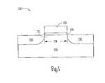
- FIG. 5shows an embodiment of a configuration of a transistor 500 having an atomic layer deposited lanthanide doped TiO x dielectric film.
- Transistor 500includes a silicon based substrate 510 with a source 520 and a drain 530 separated by a body region 532 .
- Body region 532 between source 520 and drain 530defines a channel region having a channel length 534 .
- a stack 555including a gate dielectric 540 , a floating gate 552 , a floating gate dielectric 542 , and a control gate 550 .
- Gate dielectric 540can be formed as described above with the remaining elements of the transistor 500 formed using processes known to those skilled in the art. Alternately, both gate dielectric 540 and floating gate dielectric 542 can be formed as dielectric layers containing lanthanide doped TiO x in various embodiments as described herein.
- a methodcan include forming a first conductive layer, forming a dielectric film containing lanthanide doped TiO x on the first conductive layer by depositing titanium and oxygen onto the first conductive layer by atomic layer deposition and depositing a lanthanide dopant by atomic layer deposition onto the first conductive layer containing the deposited titanium and oxygen, and forming a second conductive layer on the dielectric film.
- ALD formation of the lanthanide doped TiO x filmallows the lanthanide to be selectively doped into the TiO x film within a predetermined range for the percentage of the lanthanide in the film.
- a capacitorcan be constructed by forming a conductive layer on a substrate, forming a dielectric film containing lanthanide doped TiO x using any of the embodiments described herein, and forming another conductive layer on the dielectric film.
- Transistors, capacitors, and other devices having dielectric films containing atomic layer deposited lanthanide doped TiO x formed by the methods described abovemay be implemented into memory devices and electronic systems including information handling devices.
- Such information devicescan include wireless systems, telecommunication systems, and computers.
- An embodiment of a computer having a dielectric layer containing atomic layer deposited lanthanide doped TiO xis shown in FIGS. 6–8 and described below. While specific types of memory devices and computing devices are shown below, it will be recognized by one skilled in the art that several types of memory devices and electronic systems including information handling devices utilize the invention.
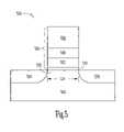
- a personal computercan include a monitor 600 , keyboard input 602 and a central processing unit 604 .
- Central processor unit 604typically includes microprocessor 706 , memory bus circuit 708 having a plurality of memory slots 712 ( a–n ), and other peripheral circuitry 710 .
- Peripheral circuitry 710permits various peripheral devices 724 to interface processor-memory bus 720 over input/output (I/O) bus 722 .
- the personal computer shown in FIGS. 6 and 7also includes at least one transistor having a dielectric layer containing atomic layer deposited lanthanide doped TiO x according an embodiment of the present invention.
- Microprocessor 706produces control and address signals to control the exchange of data between memory bus circuit 708 and microprocessor 706 and between memory bus circuit 708 and peripheral circuitry 710 . This exchange of data is accomplished over high speed memory bus 720 and over high speed I/O bus 722 .
- Coupled to memory bus 720are a plurality of memory slots 712 ( a–n ) which receive memory devices well known to those skilled in the art.
- memory slots 712a–n
- SIMMssingle in-line memory modules
- DIMMsdual in-line memory modules
- Page mode operations in a DRAMare defined by the method of accessing a row of a memory cell arrays and randomly accessing different columns of the array. Data stored at the row and column intersection can be read and output while that column is accessed. Page mode DRAMs require access steps which limit the communication speed of memory circuit 708 .
- EDOextended data output
- DDR SDRAMDDR SDRAM
- SLDRAMDirect RDRAM
- otherssuch as SRAM or Flash memories.
- FIG. 8illustrates a schematic view of an embodiment of a DRAM memory device 800 having an atomic layer deposited lanthanide doped TiO x dielectric film.
- Illustrative DRAM memory device 800is compatible with memory slots 712 ( a–n ).
- the description of DRAM memory device 800has been simplified for purposes of illustrating a DRAM memory device and is not intended to be a complete description of all the features of a DRAM. Those skilled in the art will recognize that a wide variety of memory devices may be used in the implementation of embodiments of the present invention.
- the embodiment of a DRAM memory device shown in FIG. 8includes at least one transistor having a gate dielectric containing atomic layer deposited lanthanide doped TiO x according to the teachings of the present invention.
- Control, address and data information provided over memory bus 720is further represented by individual inputs to DRAM 800 , as shown in FIG. 8 . These individual representations are illustrated by data lines 802 , address lines 804 and various discrete lines directed to control logic 806 .
- DRAM 800includes memory array 810 which in turn comprises rows and columns of addressable memory cells. Each memory cell in a row is coupled to a common word line. The word line is coupled to gates of individual transistors, where at least one transistor has a gate coupled to a gate dielectric containing atomic layer deposited lanthanide doped TiO x in accordance with the method and structure previously described above. Additionally, each memory cell in a column is coupled to a common bit line. Each cell in memory array 810 includes a storage capacitor and an access transistor as is conventional in the art.
- DRAM 800interfaces with, for example, microprocessor 706 through address lines 804 and data lines 802 .
- DRAM 800may interface with a DRAM controller, a micro-controller, a chip set or other electronic system.
- Microprocessor 706also provides a number of control signals to DRAM 800 , including but not limited to, row and column address strobe signals RAS and CAS, write enable signal WE, an output enable signal OE and other conventional control signals.
- Row address buffer 812 and row decoder 814receive and decode row addresses from row address signals provided on address lines 804 by microprocessor 706 . Each unique row address corresponds to a row of cells in memory array 810 .
- Row decoder 814includes a word line driver, an address decoder tree, and circuitry which translates a given row address received from row address buffers 812 and selectively activates the appropriate word line of memory array 810 via the word line drivers.
- Column address buffer 816 and column decoder 818receive and decode column address signals provided on address lines 804 .
- Column decoder 818also determines when a column is defective and the address of a replacement column.
- Column decoder 818is coupled to sense amplifiers 820 .
- Sense amplifiers 820are coupled to complementary pairs of bit lines of memory array 810 .
- Sense amplifiers 820are coupled to data-in buffer 822 and data-out buffer 824 .
- Data-in buffers 822 and data-out buffers 824are coupled to data lines 802 .
- data lines 802provide data to data-in buffer 822 .
- Sense amplifier 820receives data from data-in buffer 822 and stores the data in memory array 810 as a charge on a capacitor of a cell at an address specified on address lines 804 .
- DRAM 800transfers data to microprocessor 706 from memory array 810 .
- Complementary bit lines for the accessed cellare equilibrated during a precharge operation to a reference voltage provided by an equilibration circuit and a reference voltage supply.
- the charge stored in the accessed cellis then shared with the associated bit lines.
- a sense amplifier of sense amplifiers 820detects and amplifies a difference in voltage between the complementary bit lines.
- the sense amplifierpasses the amplified voltage to data-out buffer 824 .
- Control logic 806is used to control the many available functions of DRAM 800 .
- various control circuits and signals not detailed hereininitiate and synchronize DRAM 800 operation as known to those skilled in the art.
- the description of DRAM 800has been simplified for purposes of illustrating an embodiment of the present invention and is not intended to be a complete description of all the features of a DRAM.
- CMOScomplementary metal-oxide-semiconductor
- RDRAMRDRAMs
- VRAMs and EEPROMsmay be used in the implementation of embodiments of the present invention.
- the DRAM implementation described hereinis illustrative only and not intended to be exclusive or limiting.
- a dielectric film containing atomic layer deposited lanthanide doped TiO x and a method of fabricating such a dielectric filmproduce a reliable dielectric film having an equivalent oxide thickness thinner than attainable using SiO 2 .
- Dielectric films containing atomic layer deposited lanthanide doped TiO x formed using the methods described hereinare thermodynamically stable such that the dielectric films formed will have minimal reactions with a silicon substrate or other structures during processing.
- Lanthanide doped TiO x films formed by atomic layer depositioncan be amorphous and possess smooth surfaces. Such lanthanide doped TiO x films can provide enhanced electrical properties due to their smoother surface resulting in reduced leakage current. Furthermore, doping with a lanthanide such as Nd, Tb, and Dy provide for increased breakdown electric fields and decreased leakage currents than can be attained with an undoped TiO x film. Additionally, formation of the lanthanide doped TiO x films by atomic layer deposition allows for the engineering of the relative concentrations of the lanthanide dopant and the limited occurrence of an unwanted SiO 2 interfacial layer. These properties of layers containing atomic layer deposited lanthanide doped TiO x films allow for application as dielectric layers in numerous electronic devices and systems.
- Capacitors, transistors, higher level ICs or devices, and electronic systemsare constructed utilizing the novel process for forming a dielectric film having an ultra thin equivalent oxide thickness, t eq .
- Gate dielectric layers or films containing atomic layer deposited lanthanide doped TiO xare formed having a dielectric constant ( ⁇ ) substantially higher than that of silicon oxide, where the dielectric films are capable of a t eq thinner than 10 ⁇ , thinner than the expected limit for SiO 2 gate dielectrics.
- the physical thickness of the atomic layer deposited lanthanide doped TiO x dielectric filmis much larger than the SiO 2 thickness associated with the t eq limit of SiO 2 .
- Forming the relatively larger thicknessprovides advantages in processing gate dielectrics and other dielectric layers. Further, a lanthanide doped TiO x film processed in relatively low temperatures allowed by atomic layer deposition can provide amorphous dielectric films having relatively low leakage current for use as dielectric layers in electronic devices and systems.
Landscapes
- Chemical & Material Sciences (AREA)
- Engineering & Computer Science (AREA)
- General Chemical & Material Sciences (AREA)
- Chemical Kinetics & Catalysis (AREA)
- Condensed Matter Physics & Semiconductors (AREA)
- General Physics & Mathematics (AREA)
- Manufacturing & Machinery (AREA)
- Computer Hardware Design (AREA)
- Microelectronics & Electronic Packaging (AREA)
- Power Engineering (AREA)
- Physics & Mathematics (AREA)
- Metallurgy (AREA)
- Materials Engineering (AREA)
- Mechanical Engineering (AREA)
- Organic Chemistry (AREA)
- Inorganic Chemistry (AREA)
- Crystallography & Structural Chemistry (AREA)
- Semiconductor Memories (AREA)
- Formation Of Insulating Films (AREA)
- Chemical Vapour Deposition (AREA)
Abstract
Description
t=(κ/κox)teq=(κ/3.9)teq.
Thus, materials with a dielectric constant greater than that of SiO2, 3.9, will have a physical thickness that can be considerably larger than a desired teqwhile providing the desired equivalent oxide thickness. For example, an alternate dielectric material with a dielectric constant of 10 could have a thickness of about 25.6 Å to provide a teqof 10 Å, not including any depletion/inversion layer effects. Thus, a reduced equivalent oxide thickness for transistors can be realized by using dielectric materials with higher dielectric constants than SiO2.
teq=tSiO2+(κox/κ)t.
Thus, if a SiO2layer is formed in the process, the teqis again limited by a SiO2layer. In the event that a barrier layer is formed between the silicon layer and the desired dielectric in which the barrier layer prevents the formation of a SiO2layer, the teqwould be limited by the layer with the lowest dielectric constant. However, whether a single dielectric layer with a high dielectric constant or a barrier layer with a higher dielectric constant than SiO2is employed, the layer interfacing with the silicon layer must provide a high quality interface to maintain a high channel carrier mobility.
| Dielectric | Band gap | Crystal | |
| Material | Constant (κ) | Eg(eV) | Structure (s) |
| SiO2 | 3.9 | 8.9 | Amorphous |
| Si3N4 | 7 | 5.1 | Amorphous |
| Al2O3 | 9 | 8.7 | Amorphous |
| Y2O3 | 15 | 5.6 | Cubic |
| La2O3 | 30 | 4.3 | Hexagonal, Cubic |
| Ta2O5 | 26 | 4.5 | Orthorhombic |
| TiO2 | 80 | 3.5 | Tetrag. (rutile, anatase) |
| HfO2 | 25 | 5.7 | Mono., Tetrag., Cubic |
| ZrO2 | 25 | 7.8 | Mono., Tetrag., Cubic |
| Physical | Physical | Physical | Physical | |
| Thickness | Thickness | Thickness | Thickness | |
| t = 1.0 nm | t = 5.0 nm | t = 100.0 nm | t = 350 nm | |
| (1.0 × 101Å) | (5.0 × 101Å) | (1 × 10³Å) | (3.5 × 10³Å) | |
| κ | teq(Å) | teq(Å) | teq(Å) | teq(Å) |
| 50 | 0.78 | 3.90 | 78.00 | 273.00 |
| 75 | 0.52 | 2.60 | 52.00 | 182.00 |
| 100 | 0.39 | 1.95 | 39.00 | 136.50 |
| 110 | 0.35 | 1.77 | 35.45 | 124.09 |
Claims (41)
Priority Applications (2)
| Application Number | Priority Date | Filing Date | Title |
|---|---|---|---|
| US10/233,309US7084078B2 (en) | 2002-08-29 | 2002-08-29 | Atomic layer deposited lanthanide doped TiOx dielectric films |
| US11/427,569US7388246B2 (en) | 2002-08-29 | 2006-06-29 | Lanthanide doped TiOx dielectric films |
Applications Claiming Priority (1)
| Application Number | Priority Date | Filing Date | Title |
|---|---|---|---|
| US10/233,309US7084078B2 (en) | 2002-08-29 | 2002-08-29 | Atomic layer deposited lanthanide doped TiOx dielectric films |
Related Child Applications (1)
| Application Number | Title | Priority Date | Filing Date |
|---|---|---|---|
| US11/427,569DivisionUS7388246B2 (en) | 2002-08-29 | 2006-06-29 | Lanthanide doped TiOx dielectric films |
Publications (2)
| Publication Number | Publication Date |
|---|---|
| US20040043541A1 US20040043541A1 (en) | 2004-03-04 |
| US7084078B2true US7084078B2 (en) | 2006-08-01 |
Family
ID=31977210
Family Applications (2)
| Application Number | Title | Priority Date | Filing Date |
|---|---|---|---|
| US10/233,309Expired - Fee RelatedUS7084078B2 (en) | 2002-08-29 | 2002-08-29 | Atomic layer deposited lanthanide doped TiOx dielectric films |
| US11/427,569Expired - LifetimeUS7388246B2 (en) | 2002-08-29 | 2006-06-29 | Lanthanide doped TiOx dielectric films |
Family Applications After (1)
| Application Number | Title | Priority Date | Filing Date |
|---|---|---|---|
| US11/427,569Expired - LifetimeUS7388246B2 (en) | 2002-08-29 | 2006-06-29 | Lanthanide doped TiOx dielectric films |
Country Status (1)
| Country | Link |
|---|---|
| US (2) | US7084078B2 (en) |
Cited By (65)
| Publication number | Priority date | Publication date | Assignee | Title |
|---|---|---|---|---|
| US20060115993A1 (en)* | 2002-09-10 | 2006-06-01 | Samsung Electronics Co., Ltd. | Post thermal treatment methods of forming high dielectric layers over interfacial layers in integrated circuit devices |
| US20060228868A1 (en)* | 2005-03-29 | 2006-10-12 | Micron Technology, Inc. | ALD of amorphous lanthanide doped TiOx films |
| US20060292880A1 (en)* | 2005-06-24 | 2006-12-28 | Samsung Electronics Co., Ltd | Methods of fabricating p-type transistors including germanium channel regions and related devices |
| US7208804B2 (en) | 2001-08-30 | 2007-04-24 | Micron Technology, Inc. | Crystalline or amorphous medium-K gate oxides, Y203 and Gd203 |
| US7235854B2 (en) | 2002-08-15 | 2007-06-26 | Micron Technology, Inc. | Lanthanide doped TiOx dielectric films |
| US7235501B2 (en) | 2004-12-13 | 2007-06-26 | Micron Technology, Inc. | Lanthanum hafnium oxide dielectrics |
| US7312494B2 (en) | 2003-06-24 | 2007-12-25 | Micron Technology, Inc. | Lanthanide oxide / hafnium oxide dielectric layers |
| US7326980B2 (en) | 2002-08-28 | 2008-02-05 | Micron Technology, Inc. | Devices with HfSiON dielectric films which are Hf-O rich |
| US20080032465A1 (en)* | 2006-08-03 | 2008-02-07 | Micron Technology, Inc. | Deposition of ZrAION films |
| US20080087890A1 (en)* | 2006-10-16 | 2008-04-17 | Micron Technology, Inc. | Methods to form dielectric structures in semiconductor devices and resulting devices |
| US7388246B2 (en) | 2002-08-29 | 2008-06-17 | Micron Technology, Inc. | Lanthanide doped TiOx dielectric films |
| US7390756B2 (en) | 2005-04-28 | 2008-06-24 | Micron Technology, Inc. | Atomic layer deposited zirconium silicon oxide films |
| US7402876B2 (en) | 2002-12-04 | 2008-07-22 | Micron Technology, Inc. | Zr— Sn—Ti—O films |
| US7405454B2 (en) | 2003-03-04 | 2008-07-29 | Micron Technology, Inc. | Electronic apparatus with deposited dielectric layers |
| US7410910B2 (en) | 2005-08-31 | 2008-08-12 | Micron Technology, Inc. | Lanthanum aluminum oxynitride dielectric films |
| US7410668B2 (en) | 2001-03-01 | 2008-08-12 | Micron Technology, Inc. | Methods, systems, and apparatus for uniform chemical-vapor depositions |
| US7432548B2 (en) | 2006-08-31 | 2008-10-07 | Micron Technology, Inc. | Silicon lanthanide oxynitride films |
| US7446368B2 (en) | 2001-08-30 | 2008-11-04 | Micron Technology, Inc. | Deposition of metal oxide and/or low asymmetrical tunnel barrier interpoly insulators |
| US7494939B2 (en) | 2004-08-31 | 2009-02-24 | Micron Technology, Inc. | Methods for forming a lanthanum-metal oxide dielectric layer |
| US7544604B2 (en) | 2006-08-31 | 2009-06-09 | Micron Technology, Inc. | Tantalum lanthanide oxynitride films |
| US7544398B1 (en)* | 2005-04-26 | 2009-06-09 | The Regents Of The Univesity Of California | Controlled nano-doping of ultra thin films |
| US7554161B2 (en) | 2002-06-05 | 2009-06-30 | Micron Technology, Inc. | HfAlO3 films for gate dielectrics |
| US7560395B2 (en) | 2005-01-05 | 2009-07-14 | Micron Technology, Inc. | Atomic layer deposited hafnium tantalum oxide dielectrics |
| US7560793B2 (en) | 2002-05-02 | 2009-07-14 | Micron Technology, Inc. | Atomic layer deposition and conversion |
| US7563730B2 (en) | 2006-08-31 | 2009-07-21 | Micron Technology, Inc. | Hafnium lanthanide oxynitride films |
| US7572695B2 (en) | 2005-05-27 | 2009-08-11 | Micron Technology, Inc. | Hafnium titanium oxide films |
| US7575978B2 (en) | 2005-08-04 | 2009-08-18 | Micron Technology, Inc. | Method for making conductive nanoparticle charge storage element |
| US7588988B2 (en) | 2004-08-31 | 2009-09-15 | Micron Technology, Inc. | Method of forming apparatus having oxide films formed using atomic layer deposition |
| US7601649B2 (en) | 2004-08-02 | 2009-10-13 | Micron Technology, Inc. | Zirconium-doped tantalum oxide films |
| US7605030B2 (en) | 2006-08-31 | 2009-10-20 | Micron Technology, Inc. | Hafnium tantalum oxynitride high-k dielectric and metal gates |
| US7611959B2 (en) | 2002-12-04 | 2009-11-03 | Micron Technology, Inc. | Zr-Sn-Ti-O films |
| US20090272962A1 (en)* | 2008-05-01 | 2009-11-05 | Pragati Kumar | Reduction of forming voltage in semiconductor devices |
| US20090275150A1 (en)* | 2004-06-21 | 2009-11-05 | Kazuhide Hasebe | Film formation apparatus and method for semiconductor process |
| US20090273087A1 (en)* | 2008-05-01 | 2009-11-05 | Wayne French | Closed-loop sputtering controlled to enhance electrical characteristics in deposited layer |
| US20090272961A1 (en)* | 2008-05-01 | 2009-11-05 | Michael Miller | Surface treatment to improve resistive-switching characteristics |
| US7625794B2 (en) | 2003-03-31 | 2009-12-01 | Micron Technology, Inc. | Methods of forming zirconium aluminum oxide |
| US7662729B2 (en) | 2005-04-28 | 2010-02-16 | Micron Technology, Inc. | Atomic layer deposition of a ruthenium layer to a lanthanide oxide dielectric layer |
| US7670646B2 (en) | 2002-05-02 | 2010-03-02 | Micron Technology, Inc. | Methods for atomic-layer deposition |
| US7687409B2 (en) | 2005-03-29 | 2010-03-30 | Micron Technology, Inc. | Atomic layer deposited titanium silicon oxide films |
| US7709402B2 (en) | 2006-02-16 | 2010-05-04 | Micron Technology, Inc. | Conductive layers for hafnium silicon oxynitride films |
| US7719065B2 (en) | 2004-08-26 | 2010-05-18 | Micron Technology, Inc. | Ruthenium layer for a dielectric layer containing a lanthanide oxide |
| US7754618B2 (en) | 2005-02-10 | 2010-07-13 | Micron Technology, Inc. | Method of forming an apparatus having a dielectric containing cerium oxide and aluminum oxide |
| US7759747B2 (en) | 2006-08-31 | 2010-07-20 | Micron Technology, Inc. | Tantalum aluminum oxynitride high-κ dielectric |
| US20100330269A1 (en)* | 2009-06-30 | 2010-12-30 | Hanhong Chen | Titanium-Based High-K Dielectric Films |
| US7927948B2 (en) | 2005-07-20 | 2011-04-19 | Micron Technology, Inc. | Devices with nanocrystals and methods of formation |
| US7972974B2 (en) | 2006-01-10 | 2011-07-05 | Micron Technology, Inc. | Gallium lanthanide oxide films |
| US7989290B2 (en) | 2005-08-04 | 2011-08-02 | Micron Technology, Inc. | Methods for forming rhodium-based charge traps and apparatus including rhodium-based charge traps |
| US8026161B2 (en) | 2001-08-30 | 2011-09-27 | Micron Technology, Inc. | Highly reliable amorphous high-K gate oxide ZrO2 |
| US8093638B2 (en) | 2002-06-05 | 2012-01-10 | Micron Technology, Inc. | Systems with a gate dielectric having multiple lanthanide oxide layers |
| US8110469B2 (en) | 2005-08-30 | 2012-02-07 | Micron Technology, Inc. | Graded dielectric layers |
| US8168502B2 (en) | 2006-08-31 | 2012-05-01 | Micron Technology, Inc. | Tantalum silicon oxynitride high-K dielectrics and metal gates |
| US8354702B1 (en)* | 2010-02-19 | 2013-01-15 | Elpida Memory, Inc. | Inexpensive electrode materials to facilitate rutile phase titanium oxide |
| US8367506B2 (en) | 2007-06-04 | 2013-02-05 | Micron Technology, Inc. | High-k dielectrics with gold nano-particles |
| US8741698B2 (en) | 2011-11-29 | 2014-06-03 | Intermolecular, Inc. | Atomic layer deposition of zirconium oxide for forming resistive-switching materials |
| US8787066B2 (en) | 2011-10-26 | 2014-07-22 | Intermolecular, Inc. | Method for forming resistive switching memory elements with improved switching behavior |
| US8802492B2 (en) | 2011-08-29 | 2014-08-12 | Intermolecular, Inc. | Method for forming resistive switching memory elements |
| US8852996B2 (en) | 2012-12-20 | 2014-10-07 | Intermolecular, Inc. | Carbon doped resistive switching layers |
| US8853046B2 (en) | 2012-02-16 | 2014-10-07 | Intermolecular, Inc. | Using TiON as electrodes and switching layers in ReRAM devices |
| US8883557B1 (en) | 2013-09-03 | 2014-11-11 | Intermolecular, Inc. | Controlling composition of multiple oxides in resistive switching layers using atomic layer deposition |
| US8907313B2 (en) | 2012-12-18 | 2014-12-09 | Intermolecular, Inc. | Controlling ReRam forming voltage with doping |
| US9040413B2 (en) | 2012-12-13 | 2015-05-26 | Intermolecular, Inc. | Using saturated and unsaturated ALD processes to deposit oxides as ReRAM switching layer |
| US10872763B2 (en) | 2019-05-03 | 2020-12-22 | Applied Materials, Inc. | Treatments to enhance material structures |
| US11271097B2 (en) | 2019-11-01 | 2022-03-08 | Applied Materials, Inc. | Cap oxidation for FinFET formation |
| US11955332B2 (en) | 2019-05-03 | 2024-04-09 | Applied Materials, Inc. | Treatments to enhance material structures |
| US12249511B2 (en) | 2019-05-03 | 2025-03-11 | Applied Materials, Inc. | Treatments to improve device performance |
Families Citing this family (29)
| Publication number | Priority date | Publication date | Assignee | Title |
|---|---|---|---|---|
| US7068544B2 (en) | 2001-08-30 | 2006-06-27 | Micron Technology, Inc. | Flash memory with low tunnel barrier interpoly insulators |
| US6900122B2 (en) | 2001-12-20 | 2005-05-31 | Micron Technology, Inc. | Low-temperature grown high-quality ultra-thin praseodymium gate dielectrics |
| US6953730B2 (en) | 2001-12-20 | 2005-10-11 | Micron Technology, Inc. | Low-temperature grown high quality ultra-thin CoTiO3 gate dielectrics |
| US6893984B2 (en)* | 2002-02-20 | 2005-05-17 | Micron Technology Inc. | Evaporated LaA1O3 films for gate dielectrics |
| US7221586B2 (en) | 2002-07-08 | 2007-05-22 | Micron Technology, Inc. | Memory utilizing oxide nanolaminates |
| US6921702B2 (en)* | 2002-07-30 | 2005-07-26 | Micron Technology Inc. | Atomic layer deposited nanolaminates of HfO2/ZrO2 films as gate dielectrics |
| US6884739B2 (en)* | 2002-08-15 | 2005-04-26 | Micron Technology Inc. | Lanthanide doped TiOx dielectric films by plasma oxidation |
| US7183186B2 (en)* | 2003-04-22 | 2007-02-27 | Micro Technology, Inc. | Atomic layer deposited ZrTiO4 films |
| US7049192B2 (en)* | 2003-06-24 | 2006-05-23 | Micron Technology, Inc. | Lanthanide oxide / hafnium oxide dielectrics |
| KR100668832B1 (en)* | 2004-11-29 | 2007-01-16 | 주식회사 하이닉스반도체 | Capacitor Formation Method of Semiconductor Device |
| US20060125030A1 (en)* | 2004-12-13 | 2006-06-15 | Micron Technology, Inc. | Hybrid ALD-CVD of PrxOy/ZrO2 films as gate dielectrics |
| US7508648B2 (en)* | 2005-02-08 | 2009-03-24 | Micron Technology, Inc. | Atomic layer deposition of Dy doped HfO2 films as gate dielectrics |
| US7399666B2 (en)* | 2005-02-15 | 2008-07-15 | Micron Technology, Inc. | Atomic layer deposition of Zr3N4/ZrO2 films as gate dielectrics |
| US7498247B2 (en)* | 2005-02-23 | 2009-03-03 | Micron Technology, Inc. | Atomic layer deposition of Hf3N4/HfO2 films as gate dielectrics |
| US7510983B2 (en)* | 2005-06-14 | 2009-03-31 | Micron Technology, Inc. | Iridium/zirconium oxide structure |
| US7195999B2 (en)* | 2005-07-07 | 2007-03-27 | Micron Technology, Inc. | Metal-substituted transistor gates |
| US7393736B2 (en) | 2005-08-29 | 2008-07-01 | Micron Technology, Inc. | Atomic layer deposition of Zrx Hfy Sn1-x-y O2 films as high k gate dielectrics |
| US20070049023A1 (en)* | 2005-08-29 | 2007-03-01 | Micron Technology, Inc. | Zirconium-doped gadolinium oxide films |
| US7544596B2 (en) | 2005-08-30 | 2009-06-09 | Micron Technology, Inc. | Atomic layer deposition of GdScO3 films as gate dielectrics |
| US8071476B2 (en) | 2005-08-31 | 2011-12-06 | Micron Technology, Inc. | Cobalt titanium oxide dielectric films |
| US7214994B2 (en) | 2005-08-31 | 2007-05-08 | Micron Technology, Inc. | Self aligned metal gates on high-k dielectrics |
| US7582161B2 (en) | 2006-04-07 | 2009-09-01 | Micron Technology, Inc. | Atomic layer deposited titanium-doped indium oxide films |
| JP4895703B2 (en)* | 2006-06-28 | 2012-03-14 | 三洋電機株式会社 | Motor control device |
| US7749879B2 (en)* | 2006-08-03 | 2010-07-06 | Micron Technology, Inc. | ALD of silicon films on germanium |
| US7985995B2 (en) | 2006-08-03 | 2011-07-26 | Micron Technology, Inc. | Zr-substituted BaTiO3 films |
| US7582549B2 (en) | 2006-08-25 | 2009-09-01 | Micron Technology, Inc. | Atomic layer deposited barium strontium titanium oxide films |
| US20080057659A1 (en)* | 2006-08-31 | 2008-03-06 | Micron Technology, Inc. | Hafnium aluminium oxynitride high-K dielectric and metal gates |
| US8420208B2 (en)* | 2010-08-11 | 2013-04-16 | Micron Technology, Inc. | High-k dielectric material and methods of forming the high-k dielectric material |
| TWI586828B (en)* | 2012-02-10 | 2017-06-11 | 財團法人國家同步輻射研究中心 | Doping method of atomic layer deposition |
Citations (151)
| Publication number | Priority date | Publication date | Assignee | Title |
|---|---|---|---|---|
| US4058430A (en)* | 1974-11-29 | 1977-11-15 | Tuomo Suntola | Method for producing compound thin films |
| US4333808A (en) | 1979-10-30 | 1982-06-08 | International Business Machines Corporation | Method for manufacture of ultra-thin film capacitor |
| US4413022A (en) | 1979-02-28 | 1983-11-01 | Canon Kabushiki Kaisha | Method for performing growth of compound thin films |
| US5055319A (en) | 1990-04-02 | 1991-10-08 | The Regents Of The University Of California | Controlled high rate deposition of metal oxide films |
| US5572052A (en) | 1992-07-24 | 1996-11-05 | Mitsubishi Denki Kabushiki Kaisha | Electronic device using zirconate titanate and barium titanate ferroelectrics in insulating layer |
| US5698022A (en) | 1996-08-14 | 1997-12-16 | Advanced Technology Materials, Inc. | Lanthanide/phosphorus precursor compositions for MOCVD of lanthanide/phosphorus oxide films |
| US5795808A (en) | 1995-11-13 | 1998-08-18 | Hyundai Electronics Industries C., Ltd. | Method for forming shallow junction for semiconductor device |
| US5801105A (en) | 1995-08-04 | 1998-09-01 | Tdk Corporation | Multilayer thin film, substrate for electronic device, electronic device, and preparation of multilayer oxide thin film |
| US5810923A (en) | 1994-08-17 | 1998-09-22 | Tdk Corporation | Method for forming oxide thin film and the treatment of silicon substrate |
| US5840897A (en) | 1990-07-06 | 1998-11-24 | Advanced Technology Materials, Inc. | Metal complex source reagents for chemical vapor deposition |
| US5912797A (en) | 1997-09-24 | 1999-06-15 | Lucent Technologies Inc. | Dielectric materials of amorphous compositions and devices employing same |
| US5916365A (en) | 1996-08-16 | 1999-06-29 | Sherman; Arthur | Sequential chemical vapor deposition |
| US6020024A (en) | 1997-08-04 | 2000-02-01 | Motorola, Inc. | Method for forming high dielectric constant metal oxides |
| US6025627A (en) | 1998-05-29 | 2000-02-15 | Micron Technology, Inc. | Alternate method and structure for improved floating gate tunneling devices |
| US6093944A (en)* | 1998-06-04 | 2000-07-25 | Lucent Technologies Inc. | Dielectric materials of amorphous compositions of TI-O2 doped with rare earth elements and devices employing same |
| US6110529A (en) | 1990-07-06 | 2000-08-29 | Advanced Tech Materials | Method of forming metal films on a substrate by chemical vapor deposition |
| US6200893B1 (en) | 1999-03-11 | 2001-03-13 | Genus, Inc | Radical-assisted sequential CVD |
| US6203613B1 (en) | 1999-10-19 | 2001-03-20 | International Business Machines Corporation | Atomic layer deposition with nitrate containing precursors |
| US6207589B1 (en) | 1999-07-19 | 2001-03-27 | Sharp Laboratories Of America, Inc. | Method of forming a doped metal oxide dielectric film |
| US6211035B1 (en) | 1998-09-09 | 2001-04-03 | Texas Instruments Incorporated | Integrated circuit and method |
| US6225168B1 (en) | 1998-06-04 | 2001-05-01 | Advanced Micro Devices, Inc. | Semiconductor device having metal gate electrode and titanium or tantalum nitride gate dielectric barrier layer and process of fabrication thereof |
| EP1096042A1 (en) | 1999-10-25 | 2001-05-02 | Motorola, Inc. | Method for fabricating a semiconductor structure including a metal oxide interface with silicon |
| US20010009695A1 (en) | 2000-01-18 | 2001-07-26 | Saanila Ville Antero | Process for growing metalloid thin films |
| US6297539B1 (en) | 1999-07-19 | 2001-10-02 | Sharp Laboratories Of America, Inc. | Doped zirconia, or zirconia-like, dielectric film transistor structure and deposition method for same |
| US20010030352A1 (en) | 2000-02-29 | 2001-10-18 | Alexander Ruf | Method for increasing the capacitance in a storage trench and trench capacitor having increased capacitance |
| US20010042505A1 (en) | 1999-06-16 | 2001-11-22 | Micron Technology, Inc. | Precursor mixtures for use in preparing layers on substrates |
| US20020001971A1 (en) | 2000-06-27 | 2002-01-03 | Hag-Ju Cho | Methods of manufacturing integrated circuit devices that include a metal oxide layer disposed on another layer to protect the other layer from diffusion of impurities and integrated circuit devices manufactured using same |
| US20020024080A1 (en) | 2000-08-31 | 2002-02-28 | Derderian Garo J. | Capacitor fabrication methods and capacitor constructions |
| US20020025628A1 (en) | 2000-08-31 | 2002-02-28 | Derderian Garo J. | Capacitor fabrication methods and capacitor constructions |
| WO2002031875A2 (en) | 2000-10-10 | 2002-04-18 | Asm America, Inc. | Dielectric interface films and methods therefor |
| US20020046705A1 (en) | 2000-08-31 | 2002-04-25 | Gurtej Sandhu | Atomic layer doping apparatus and method |
| US6387712B1 (en) | 1996-06-26 | 2002-05-14 | Tdk Corporation | Process for preparing ferroelectric thin films |
| US6391769B1 (en) | 1998-08-19 | 2002-05-21 | Samsung Electronics Co., Ltd. | Method for forming metal interconnection in semiconductor device and interconnection structure fabricated thereby |
| WO2001097257A3 (en) | 2000-06-12 | 2002-05-23 | Motorola Inc | Dual metal gate transistors for cmos process |
| US20020068466A1 (en) | 2000-12-06 | 2002-06-06 | Seung-Hwan Lee | Methods of forming thin films by atomic layer deposition |
| US20020086507A1 (en) | 2000-12-29 | 2002-07-04 | Park Dae Gyu | Method of forming a metal gate in a semiconductor device |
| US20020089023A1 (en) | 2001-01-05 | 2002-07-11 | Motorola, Inc. | Low leakage current metal oxide-nitrides and method of fabricating same |
| US20020100418A1 (en) | 2000-05-12 | 2002-08-01 | Gurtej Sandhu | Versatile atomic layer deposition apparatus |
| US20020102818A1 (en) | 2000-08-31 | 2002-08-01 | Sandhu Gurtej S. | Deposition methods and apparatuses providing surface activation |
| US6432779B1 (en) | 2000-05-18 | 2002-08-13 | Motorola, Inc. | Selective removal of a metal oxide dielectric |
| US20020111001A1 (en) | 2001-02-09 | 2002-08-15 | Micron Technology, Inc. | Formation of metal oxide gate dielectric |
| US6441417B1 (en) | 2001-03-28 | 2002-08-27 | Sharp Laboratories Of America, Inc. | Single c-axis PGO thin film on ZrO2 for non-volatile memory applications and methods of making the same |
| US6444592B1 (en) | 2000-06-20 | 2002-09-03 | International Business Machines Corporation | Interfacial oxidation process for high-k gate dielectric process integration |
| US20020122885A1 (en) | 2001-03-01 | 2002-09-05 | Micron Technology, Inc. | Methods, systems, and apparatus for uniform chemical-vapor depositions |
| US6448192B1 (en) | 2001-04-16 | 2002-09-10 | Motorola, Inc. | Method for forming a high dielectric constant material |
| US6451641B1 (en) | 2002-02-27 | 2002-09-17 | Advanced Micro Devices, Inc. | Non-reducing process for deposition of polysilicon gate electrode over high-K gate dielectric material |
| US6458701B1 (en) | 1999-10-20 | 2002-10-01 | Samsung Electronics Co., Ltd. | Method for forming metal layer of semiconductor device using metal halide gas |
| US6461436B1 (en) | 2001-10-15 | 2002-10-08 | Micron Technology, Inc. | Apparatus and process of improving atomic layer deposition chamber performance |
| US20020146916A1 (en) | 2001-03-29 | 2002-10-10 | Kiyoshi Irino | Semiconductor device having a high-dielectric gate insulation film and fabrication process thereof |
| US6465334B1 (en) | 2000-10-05 | 2002-10-15 | Advanced Micro Devices, Inc. | Enhanced electroless deposition of dielectric precursor materials for use in in-laid gate MOS transistors |
| US20020155688A1 (en) | 2001-04-20 | 2002-10-24 | Ahn Kie Y. | Highly reliable gate oxide and method of fabrication |
| US20020164420A1 (en) | 2002-02-25 | 2002-11-07 | Derderian Garo J. | Deposition methods and apparatus for improved delivery of metastable species |
| US20020192975A1 (en) | 2001-06-13 | 2002-12-19 | Ahn Kie Y. | Dielectric layer forming method and devices formed therewith |
| US20030001241A1 (en) | 2000-01-18 | 2003-01-02 | Agere Systems Guardian Corp. | Semiconductor device and method of fabrication |
| US6509280B2 (en) | 2001-02-22 | 2003-01-21 | Samsung Electronics Co., Ltd. | Method for forming a dielectric layer of a semiconductor device |
| US20030017717A1 (en) | 2001-07-18 | 2003-01-23 | Ahn Kie Y. | Methods for forming dielectric materials and methods for forming semiconductor devices |
| US6521911B2 (en) | 2000-07-20 | 2003-02-18 | North Carolina State University | High dielectric constant metal silicates formed by controlled metal-surface reactions |
| US6527866B1 (en) | 2000-02-09 | 2003-03-04 | Conductus, Inc. | Apparatus and method for deposition of thin films |
| US20030045060A1 (en) | 2001-08-30 | 2003-03-06 | Micron Technology, Inc. | Crystalline or amorphous medium-k gate oxides, Y2O3 and Gd2O3 |
| US20030045078A1 (en) | 2001-08-30 | 2003-03-06 | Micron Technology, Inc. | Highly reliable amorphous high-K gate oxide ZrO2 |
| US20030042526A1 (en) | 2001-08-29 | 2003-03-06 | Micron Technology, Inc. | Method of improved high K dielectric-polysilicon interface for CMOS devices |
| US20030043637A1 (en) | 2001-08-30 | 2003-03-06 | Micron Technology, Inc | Flash memory with low tunnel barrier interpoly insulators |
| US20030045082A1 (en) | 2001-08-30 | 2003-03-06 | Micron Technology, Inc. | Atomic layer deposition of metal oxide and/or low asymmetrical tunnel barrier interploy insulators |
| US6531354B2 (en) | 2000-01-19 | 2003-03-11 | North Carolina State University | Lanthanum oxide-based gate dielectrics for integrated circuit field effect transistors |
| US20030048666A1 (en) | 2001-08-30 | 2003-03-13 | Micron Technology, Inc. | Graded composition metal oxide tunnel barrier interpoly insulators |
| US20030049942A1 (en) | 2001-08-31 | 2003-03-13 | Suvi Haukka | Low temperature gate stack |
| US6534357B1 (en) | 2000-11-09 | 2003-03-18 | Micron Technology, Inc. | Methods for forming conductive structures and structures regarding same |
| US6537613B1 (en) | 2000-04-10 | 2003-03-25 | Air Products And Chemicals, Inc. | Process for metal metalloid oxides and nitrides with compositional gradients |
| US6538330B1 (en) | 1998-08-04 | 2003-03-25 | Micron Technology, Inc. | Multilevel semiconductor-on-insulator structures and circuits |
| US20030059535A1 (en) | 2001-09-25 | 2003-03-27 | Lee Luo | Cycling deposition of low temperature films in a cold wall single wafer process chamber |
| US6541079B1 (en) | 1999-10-25 | 2003-04-01 | International Business Machines Corporation | Engineered high dielectric constant oxide and oxynitride heterostructure gate dielectrics by an atomic beam deposition technique |
| US6551893B1 (en) | 2001-11-27 | 2003-04-22 | Micron Technology, Inc. | Atomic layer deposition of capacitor dielectric |
| US6551929B1 (en) | 2000-06-28 | 2003-04-22 | Applied Materials, Inc. | Bifurcated deposition process for depositing refractory metal layers employing atomic layer deposition and chemical vapor deposition techniques |
| US6559472B2 (en) | 2000-11-21 | 2003-05-06 | Micron Technology, Inc. | Film composition |
| US20030104666A1 (en) | 2001-02-05 | 2003-06-05 | International Business Machines Corporation | Method for forming dielectric stack without interfacial layer |
| US20030119291A1 (en) | 2001-12-20 | 2003-06-26 | Micron Technology, Inc. | Low-temperature grown high-quality ultra-thin praseodymium gate dielectrics |
| US20030119313A1 (en) | 2000-12-28 | 2003-06-26 | Micron Technology, Inc. | Processes to form a metallic film stack |
| US20030119246A1 (en) | 2001-12-20 | 2003-06-26 | Micron Technology, Inc. | Low-temperature grown high quality ultra-thin CoTiO3 gate dielectrics |
| US6586349B1 (en) | 2002-02-21 | 2003-07-01 | Advanced Micro Devices, Inc. | Integrated process for fabrication of graded composite dielectric material layers for semiconductor devices |
| US6586792B2 (en) | 2001-03-15 | 2003-07-01 | Micron Technology, Inc. | Structures, methods, and systems for ferroelectric memory transistors |
| US6592942B1 (en) | 2000-07-07 | 2003-07-15 | Asm International N.V. | Method for vapour deposition of a film onto a substrate |
| US20030132491A1 (en) | 2002-01-17 | 2003-07-17 | Micron Technology, Inc. | Highly reliable amorphous high-K gate dielectric ZrOxNy |
| US6602338B2 (en) | 2000-09-18 | 2003-08-05 | National Science Council | Titanium dioxide film co-doped with yttrium and erbium and method for producing the same |
| US20030157764A1 (en) | 2002-02-20 | 2003-08-21 | Micron Technology, Inc. | Evaporated LaA1O3 films for gate dielectrics |
| US6613656B2 (en) | 2001-02-13 | 2003-09-02 | Micron Technology, Inc. | Sequential pulse deposition |
| US20030170389A1 (en) | 2002-03-05 | 2003-09-11 | Sandhu Gurtej S. | Atomic layer deposition with point of use generated reactive gas species |
| US20030170403A1 (en) | 2002-03-11 | 2003-09-11 | Doan Trung Tri | Atomic layer deposition apparatus and method |
| US6620670B2 (en) | 2002-01-18 | 2003-09-16 | Applied Materials, Inc. | Process conditions and precursors for atomic layer deposition (ALD) of AL2O3 |
| US6627503B2 (en) | 2000-02-11 | 2003-09-30 | Sharp Laboratories Of America, Inc. | Method of forming a multilayer dielectric stack |
| US6627260B2 (en) | 2000-07-19 | 2003-09-30 | Micron Technology, Inc. | Deposition methods |
| US20030183156A1 (en) | 2002-03-26 | 2003-10-02 | Dando Ross S. | Chemical vapor deposition methods, atomic layer deposition methods, and valve assemblies for use with a reactive precursor in semiconductor processing |
| US6632279B1 (en) | 1999-10-14 | 2003-10-14 | Asm Microchemistry, Oy | Method for growing thin oxide films |
| US20030194862A1 (en) | 2002-04-11 | 2003-10-16 | Mardian Allen P. | Chemical vapor deposition methods, and atomic layer deposition method |
| US20030193061A1 (en) | 2000-08-03 | 2003-10-16 | Hans-Joerg Osten | Electronic component and method for producing an electronic component |
| US6638859B2 (en) | 1999-12-22 | 2003-10-28 | Genus, Inc. | Apparatus and method to achieve continuous interface and ultrathin film during atomic layer deposition |
| US6639267B2 (en) | 2001-08-30 | 2003-10-28 | Micron Technology, Inc. | Capacitor dielectric having perovskite-type crystalline structure |
| US20030203626A1 (en) | 2002-04-25 | 2003-10-30 | Derderian Garo J. | Apparatus and method for forming thin layers of materials on micro-device workpieces |
| WO2002043115A8 (en) | 2000-11-24 | 2003-10-30 | Asm Inc | Surface preparation prior to deposition |
| US20030207540A1 (en) | 2002-05-02 | 2003-11-06 | Micron Technology, Inc. | Atomic layer-deposited laaio3 films for gate dielectrics |
| US20030207593A1 (en) | 2002-05-02 | 2003-11-06 | Micron Technology, Inc. | Atomic layer deposition and conversion |
| US20030207032A1 (en) | 2002-05-02 | 2003-11-06 | Micron Technology, Inc. | Methods, systems, and apparatus for atomic-layer deposition of aluminum oxides in integrated circuits |
| US6645882B1 (en) | 2002-01-17 | 2003-11-11 | Advanced Micro Devices, Inc. | Preparation of composite high-K/standard-K dielectrics for semiconductor devices |
| US6652924B2 (en) | 1996-08-16 | 2003-11-25 | Licensee For Microelectronics: Asm America, Inc. | Sequential chemical vapor deposition |
| US20030224600A1 (en) | 2002-03-04 | 2003-12-04 | Wei Cao | Sequential deposition of tantalum nitride using a tantalum-containing precursor and a nitrogen-containing precursor |
| US20030222300A1 (en) | 2002-03-06 | 2003-12-04 | Micron Technology, Inc. | Capacitor constructions, semiconductor constructions, and methods of forming electrical contacts and semiconductor constructions |
| US20030228747A1 (en) | 2002-06-05 | 2003-12-11 | Micron Technology, Inc. | Pr2O3-based la-oxide gate dielectrics |
| US20030227033A1 (en) | 2002-06-05 | 2003-12-11 | Micron Technology, Inc. | Atomic layer-deposited HfA1O3 films for gate dielectrics |
| US20030232511A1 (en) | 2002-06-14 | 2003-12-18 | Applied Materials, Inc. | ALD metal oxide deposition process using direct oxidation |
| US20030235961A1 (en) | 2002-04-17 | 2003-12-25 | Applied Materials, Inc. | Cyclical sequential deposition of multicomponent films |
| US6673701B1 (en) | 2002-08-27 | 2004-01-06 | Micron Technology, Inc. | Atomic layer deposition methods |
| US6674138B1 (en) | 2001-12-31 | 2004-01-06 | Advanced Micro Devices, Inc. | Use of high-k dielectric materials in modified ONO structure for semiconductor devices |
| US20040004245A1 (en) | 2002-07-08 | 2004-01-08 | Micron Technology, Inc. | Memory utilizing oxide-conductor nanolaminates |
| US20040004859A1 (en) | 2002-07-08 | 2004-01-08 | Micron Technology, Inc. | Memory utilizing oxide nanolaminates |
| US20040004247A1 (en) | 2002-07-08 | 2004-01-08 | Micron Technology, Inc. | Memory utilizing oxide-nitride nanolaminates |
| US20040009679A1 (en) | 2001-01-19 | 2004-01-15 | Yeo Jae-Hyun | Method of forming material using atomic layer deposition and method of forming capacitor of semiconductor device using the same |
| US20040023461A1 (en) | 2002-07-30 | 2004-02-05 | Micron Technology, Inc. | Atomic layer deposited nanolaminates of HfO2/ZrO2 films as gate dielectrics |
| US20040033701A1 (en)* | 2002-08-15 | 2004-02-19 | Micron Technology, Inc. | Lanthanide doped tiox dielectric films |
| US20040033681A1 (en) | 2002-08-15 | 2004-02-19 | Micron Technology, Inc. | Lanthanide doped TiOx dielectric films by plasma oxidation |
| US6696332B2 (en) | 2001-12-26 | 2004-02-24 | Texas Instruments Incorporated | Bilayer deposition to avoid unwanted interfacial reactions during high K gate dielectric processing |
| US20040038525A1 (en) | 2002-08-26 | 2004-02-26 | Shuang Meng | Enhanced atomic layer deposition |
| US20040038554A1 (en) | 2002-08-21 | 2004-02-26 | Ahn Kie Y. | Composite dielectric forming methods and composite dielectrics |
| US20040043635A1 (en) | 2002-08-28 | 2004-03-04 | Micron Technology, Inc. | Systems and methods for forming metal oxides using metal diketonates and/or ketoimines |
| US20040043569A1 (en) | 2002-08-28 | 2004-03-04 | Ahn Kie Y. | Atomic layer deposited HfSiON dielectric films |
| US6709989B2 (en) | 2001-06-21 | 2004-03-23 | Motorola, Inc. | Method for fabricating a semiconductor structure including a metal oxide interface with silicon |
| US6713846B1 (en)* | 2001-01-26 | 2004-03-30 | Aviza Technology, Inc. | Multilayer high κ dielectric films |
| US20040065255A1 (en) | 2002-10-02 | 2004-04-08 | Applied Materials, Inc. | Cyclical layer deposition system |
| US20040110391A1 (en) | 2002-12-04 | 2004-06-10 | Micron Technology, Inc. | Atomic layer deposited Zr-Sn-Ti-O films |
| US20040110348A1 (en) | 2002-12-04 | 2004-06-10 | Micron Technology, Inc. | Atomic layer deposited Zr-Sn-Ti-O films using TiI4 |
| US6750066B1 (en) | 2002-04-08 | 2004-06-15 | Advanced Micro Devices, Inc. | Precision high-K intergate dielectric layer |
| US6754108B2 (en) | 2001-08-30 | 2004-06-22 | Micron Technology, Inc. | DRAM cells with repressed floating gate memory, low tunnel barrier interpoly insulators |
| US20040134365A1 (en) | 2002-12-12 | 2004-07-15 | Konica Minolta Holdings, Inc. | Printing plate material |
| US6767582B1 (en) | 1999-10-15 | 2004-07-27 | Asm International Nv | Method of modifying source chemicals in an ald process |
| US20040144980A1 (en) | 2003-01-27 | 2004-07-29 | Ahn Kie Y. | Atomic layer deposition of metal oxynitride layers as gate dielectrics and semiconductor device structures utilizing metal oxynitride layers |
| US6777353B2 (en) | 2000-04-14 | 2004-08-17 | Asm Microchemistry Oy | Process for producing oxide thin films |
| US6778441B2 (en) | 2001-08-30 | 2004-08-17 | Micron Technology, Inc. | Integrated circuit memory device and method |
| US6780704B1 (en) | 1999-12-03 | 2004-08-24 | Asm International Nv | Conformal thin films over textured capacitor electrodes |
| US6787370B2 (en) | 1999-08-26 | 2004-09-07 | Micron Technology, Inc. | Method of forming a weak ferroelectric transistor |
| US20040175882A1 (en) | 2003-03-04 | 2004-09-09 | Micron Technology, Inc. | Atomic layer deposited dielectric layers |
| US6800567B2 (en) | 2001-08-27 | 2004-10-05 | Hynix Semiconductor Inc. | Method for forming polyatomic layers |
| US6804136B2 (en) | 2002-06-21 | 2004-10-12 | Micron Technology, Inc. | Write once read only memory employing charge trapping in insulators |
| US20040214399A1 (en) | 2003-04-22 | 2004-10-28 | Micron Technology, Inc. | Atomic layer deposited ZrTiO4 films |
| US6812100B2 (en) | 2002-03-13 | 2004-11-02 | Micron Technology, Inc. | Evaporation of Y-Si-O films for medium-k dielectrics |
| US6821873B2 (en) | 2002-01-10 | 2004-11-23 | Texas Instruments Incorporated | Anneal sequence for high-κ film property optimization |
| US20040262700A1 (en) | 2003-06-24 | 2004-12-30 | Micron Technology, Inc. | Lanthanide oxide / hafnium oxide dielectrics |
| US20050020017A1 (en) | 2003-06-24 | 2005-01-27 | Micron Technology, Inc. | Lanthanide oxide / hafnium oxide dielectric layers |
| US20050023595A1 (en) | 2001-08-30 | 2005-02-03 | Micron Technology, Inc. | Programmable array logic or memory devices with asymmetrical tunnel barriers |
| US20050023602A1 (en) | 2001-08-30 | 2005-02-03 | Micron Technology, Inc. | Programmable array logic or memory with p-channel devices and asymmetrical tunnel barriers |
| US20050054165A1 (en) | 2003-03-31 | 2005-03-10 | Micron Technology, Inc. | Atomic layer deposited ZrAlxOy dielectric layers |
| US20050077519A1 (en) | 2003-10-10 | 2005-04-14 | Kie Ahn | Lanthanide oxide/zirconium oxide atomic layer deposited nanolaminate gate dielectrics |
| US6888739B2 (en) | 2002-06-21 | 2005-05-03 | Micron Technology Inc. | Nanocrystal write once read only memory for archival storage |
| US20050138262A1 (en) | 2003-12-18 | 2005-06-23 | Micron Technology, Inc. | Flash memory having a high-permittivity tunnel dielectric |
Family Cites Families (103)
| Publication number | Priority date | Publication date | Assignee | Title |
|---|---|---|---|---|
| US721994A (en)* | 1902-08-15 | 1903-03-03 | Abner D Baker | Valve-gear for engines. |
| US2501563A (en) | 1946-02-20 | 1950-03-21 | Libbey Owens Ford Glass Co | Method of forming strongly adherent metallic compound films by glow discharge |
| DE3626468A1 (en) | 1986-08-05 | 1988-02-11 | Hoechst Ag | METHOD AND TEST KIT FOR DETERMINING FREE ACTIVE INGREDIENTS IN BIOLOGICAL LIQUIDS |
| JPH07120719B2 (en) | 1987-12-02 | 1995-12-20 | 三菱電機株式会社 | Semiconductor memory device |
| EP0540993A1 (en) | 1991-11-06 | 1993-05-12 | Ramtron International Corporation | Structure and fabrication of high transconductance MOS field effect transistor using a buffer layer/ferroelectric/buffer layer stack as the gate dielectric |
| TW235363B (en) | 1993-01-25 | 1994-12-01 | Hitachi Seisakusyo Kk | |
| US5439524A (en) | 1993-04-05 | 1995-08-08 | Vlsi Technology, Inc. | Plasma processing apparatus |
| JP3328389B2 (en) | 1993-09-14 | 2002-09-24 | 康夫 垂井 | Manufacturing method of ferroelectric thin film |
| FR2722566B1 (en) | 1994-07-13 | 1996-08-23 | Europ Gas Turbines Sa | DYNAMIC MOVEMENT SENSOR, USES OF SUCH A SENSOR AND METHOD FOR MEASURING THE MOVEMENT OF A SURFACE |
| US5783716A (en) | 1996-06-28 | 1998-07-21 | Advanced Technology Materials, Inc. | Platinum source compositions for chemical vapor deposition of platinum |
| JPH0945624A (en) | 1995-07-27 | 1997-02-14 | Tokyo Electron Ltd | Leaf-type heat treating system |
| US5714766A (en) | 1995-09-29 | 1998-02-03 | International Business Machines Corporation | Nano-structure memory device |
| US6429120B1 (en) | 2000-01-18 | 2002-08-06 | Micron Technology, Inc. | Methods and apparatus for making integrated-circuit wiring from copper, silver, gold, and other metals |
| US5923056A (en) | 1996-10-10 | 1999-07-13 | Lucent Technologies Inc. | Electronic components with doped metal oxide dielectric materials and a process for making electronic components with doped metal oxide dielectric materials |
| US5879459A (en) | 1997-08-29 | 1999-03-09 | Genus, Inc. | Vertically-stacked process reactor and cluster tool system for atomic layer deposition |
| US6034015A (en) | 1997-05-14 | 2000-03-07 | Georgia Tech Research Corporation | Ceramic compositions for microwave wireless communication |
| US6350672B1 (en) | 1997-07-28 | 2002-02-26 | United Microelectronics Corp. | Interconnect structure with gas dielectric compatible with unlanded vias |
| US6333556B1 (en) | 1997-10-09 | 2001-12-25 | Micron Technology, Inc. | Insulating materials |
| US6858526B2 (en) | 1998-07-14 | 2005-02-22 | Micron Technology, Inc. | Methods of forming materials between conductive electrical components, and insulating materials |
| US6350704B1 (en) | 1997-10-14 | 2002-02-26 | Micron Technology Inc. | Porous silicon oxycarbide integrated circuit insulator |
| KR100268936B1 (en) | 1997-12-16 | 2000-10-16 | 김영환 | A method of forming for quantum dot of semiconductor device |
| KR100269328B1 (en) | 1997-12-31 | 2000-10-16 | 윤종용 | Method for forming conductive layer using atomic layer deposition process |
| US6150188A (en) | 1998-02-26 | 2000-11-21 | Micron Technology Inc. | Integrated circuits using optical fiber interconnects formed through a semiconductor wafer and methods for forming same |
| US6289842B1 (en) | 1998-06-22 | 2001-09-18 | Structured Materials Industries Inc. | Plasma enhanced chemical vapor deposition system |
| US6710538B1 (en) | 1998-08-26 | 2004-03-23 | Micron Technology, Inc. | Field emission display having reduced power requirements and method |
| US6063705A (en) | 1998-08-27 | 2000-05-16 | Micron Technology, Inc. | Precursor chemistries for chemical vapor deposition of ruthenium and ruthenium oxide |
| US6141260A (en) | 1998-08-27 | 2000-10-31 | Micron Technology, Inc. | Single electron resistor memory device and method for use thereof |
| US6281042B1 (en) | 1998-08-31 | 2001-08-28 | Micron Technology, Inc. | Structure and method for a high performance electronic packaging assembly |
| US6225237B1 (en) | 1998-09-01 | 2001-05-01 | Micron Technology, Inc. | Method for forming metal-containing films using metal complexes with chelating O- and/or N-donor ligands |
| US6274937B1 (en) | 1999-02-01 | 2001-08-14 | Micron Technology, Inc. | Silicon multi-chip module packaging with integrated passive components and method of making |
| US6291341B1 (en) | 1999-02-12 | 2001-09-18 | Micron Technology, Inc. | Method for PECVD deposition of selected material films |
| US6713329B1 (en) | 1999-05-10 | 2004-03-30 | The Trustees Of Princeton University | Inverter made of complementary p and n channel transistors using a single directly-deposited microcrystalline silicon film |
| US6495878B1 (en) | 1999-08-02 | 2002-12-17 | Symetrix Corporation | Interlayer oxide containing thin films for high dielectric constant application |
| US6812157B1 (en) | 1999-06-24 | 2004-11-02 | Prasad Narhar Gadgil | Apparatus for atomic layer chemical vapor deposition |
| US6556962B1 (en) | 1999-07-02 | 2003-04-29 | Intel Corporation | Method for reducing network costs and its application to domino circuits |
| US6709968B1 (en) | 2000-08-16 | 2004-03-23 | Micron Technology, Inc. | Microelectronic device with package with conductive elements and associated method of manufacture |
| US6670719B2 (en) | 1999-08-25 | 2003-12-30 | Micron Technology, Inc. | Microelectronic device package filled with liquid or pressurized gas and associated method of manufacture |
| US6337237B1 (en) | 1999-09-01 | 2002-01-08 | Micron Technology, Inc. | Capacitor processing method and DRAM processing method |
| WO2001050510A2 (en) | 2000-01-06 | 2001-07-12 | Applied Materials, Inc. | Low thermal budget metal oxide deposition for capacitor structures |
| US6297103B1 (en) | 2000-02-28 | 2001-10-02 | Micron Technology, Inc. | Structure and method for dual gate oxide thicknesses |
| US6380080B2 (en) | 2000-03-08 | 2002-04-30 | Micron Technology, Inc. | Methods for preparing ruthenium metal films |
| US6642567B1 (en) | 2000-08-31 | 2003-11-04 | Micron Technology, Inc. | Devices containing zirconium-platinum-containing materials and methods for preparing such materials and devices |
| US6346477B1 (en) | 2001-01-09 | 2002-02-12 | Research Foundation Of Suny - New York | Method of interlayer mediated epitaxy of cobalt silicide from low temperature chemical vapor deposition of cobalt |
| US6858865B2 (en) | 2001-02-23 | 2005-02-22 | Micron Technology, Inc. | Doped aluminum oxide dielectrics |
| US6706608B2 (en) | 2001-02-28 | 2004-03-16 | Micron Technology, Inc. | Memory cell capacitors having an over/under configuration |
| US6696360B2 (en) | 2001-03-15 | 2004-02-24 | Micron Technology, Inc. | Barrier-metal-free copper damascene technology using atomic hydrogen enhanced reflow |
| US20050145959A1 (en) | 2001-03-15 | 2005-07-07 | Leonard Forbes | Technique to mitigate short channel effects with vertical gate transistor with different gate materials |
| US6454912B1 (en) | 2001-03-15 | 2002-09-24 | Micron Technology, Inc. | Method and apparatus for the fabrication of ferroelectric films |
| WO2002090614A1 (en) | 2001-03-20 | 2002-11-14 | Mattson Technology, Inc. | Method for depositing a coating having a relatively high dielectric constant onto a substrate |
| US6541280B2 (en) | 2001-03-20 | 2003-04-01 | Motorola, Inc. | High K dielectric film |
| US6770923B2 (en) | 2001-03-20 | 2004-08-03 | Freescale Semiconductor, Inc. | High K dielectric film |
| US6531324B2 (en) | 2001-03-28 | 2003-03-11 | Sharp Laboratories Of America, Inc. | MFOS memory transistor & method of fabricating same |
| US6602720B2 (en) | 2001-03-28 | 2003-08-05 | Sharp Laboratories Of America, Inc. | Single transistor ferroelectric transistor structure with high-K insulator and method of fabricating same |
| JP4628580B2 (en)* | 2001-04-18 | 2011-02-09 | 信越半導体株式会社 | Manufacturing method of bonded substrate |
| US6465853B1 (en) | 2001-05-08 | 2002-10-15 | Motorola, Inc. | Method for making semiconductor device |
| US6759081B2 (en) | 2001-05-11 | 2004-07-06 | Asm International, N.V. | Method of depositing thin films for magnetic heads |
| US6552383B2 (en) | 2001-05-11 | 2003-04-22 | Micron Technology, Inc. | Integrated decoupling capacitors |
| US6852194B2 (en) | 2001-05-21 | 2005-02-08 | Tokyo Electron Limited | Processing apparatus, transferring apparatus and transferring method |
| US7037574B2 (en) | 2001-05-23 | 2006-05-02 | Veeco Instruments, Inc. | Atomic layer deposition for fabricating thin films |
| US20030008243A1 (en) | 2001-07-09 | 2003-01-09 | Micron Technology, Inc. | Copper electroless deposition technology for ULSI metalization |
| US6919266B2 (en) | 2001-07-24 | 2005-07-19 | Micron Technology, Inc. | Copper technology for ULSI metallization |
| US6697819B2 (en)* | 2001-07-30 | 2004-02-24 | International Business Machines Corporation | Reusable database access component |
| JP4666912B2 (en) | 2001-08-06 | 2011-04-06 | エー・エス・エムジニテックコリア株式会社 | Plasma reinforced atomic layer deposition apparatus and thin film forming method using the same |
| US7160817B2 (en)* | 2001-08-30 | 2007-01-09 | Micron Technology, Inc. | Dielectric material forming methods |
| US7541005B2 (en) | 2001-09-26 | 2009-06-02 | Siemens Energy Inc. | Catalytic thermal barrier coatings |
| US7220312B2 (en) | 2002-03-13 | 2007-05-22 | Micron Technology, Inc. | Methods for treating semiconductor substrates |
| US6784101B1 (en) | 2002-05-16 | 2004-08-31 | Advanced Micro Devices Inc | Formation of high-k gate dielectric layers for MOS devices fabricated on strained lattice semiconductor substrates with minimized stress relaxation |
| US6617639B1 (en) | 2002-06-21 | 2003-09-09 | Advanced Micro Devices, Inc. | Use of high-K dielectric material for ONO and tunnel oxide to improve floating gate flash memory coupling |
| US6828632B2 (en) | 2002-07-18 | 2004-12-07 | Micron Technology, Inc. | Stable PD-SOI devices and methods |
| US7084078B2 (en) | 2002-08-29 | 2006-08-01 | Micron Technology, Inc. | Atomic layer deposited lanthanide doped TiOx dielectric films |
| US6884685B2 (en) | 2003-02-14 | 2005-04-26 | Freescale Semiconductors, Inc. | Radical oxidation and/or nitridation during metal oxide layer deposition process |
| US8323754B2 (en) | 2004-05-21 | 2012-12-04 | Applied Materials, Inc. | Stabilization of high-k dielectric materials |
| US7323424B2 (en) | 2004-06-29 | 2008-01-29 | Micron Technology, Inc. | Semiconductor constructions comprising cerium oxide and titanium oxide |
| US7601649B2 (en) | 2004-08-02 | 2009-10-13 | Micron Technology, Inc. | Zirconium-doped tantalum oxide films |
| US7151294B2 (en) | 2004-08-03 | 2006-12-19 | Micron Technology, Inc. | High density stepped, non-planar flash memory |
| US7164168B2 (en) | 2004-08-03 | 2007-01-16 | Micron Technology, Inc. | Non-planar flash memory having shielding between floating gates |
| US7081421B2 (en) | 2004-08-26 | 2006-07-25 | Micron Technology, Inc. | Lanthanide oxide dielectric layer |
| US7494939B2 (en) | 2004-08-31 | 2009-02-24 | Micron Technology, Inc. | Methods for forming a lanthanum-metal oxide dielectric layer |
| US7588988B2 (en) | 2004-08-31 | 2009-09-15 | Micron Technology, Inc. | Method of forming apparatus having oxide films formed using atomic layer deposition |
| US7235501B2 (en) | 2004-12-13 | 2007-06-26 | Micron Technology, Inc. | Lanthanum hafnium oxide dielectrics |
| US20060125030A1 (en) | 2004-12-13 | 2006-06-15 | Micron Technology, Inc. | Hybrid ALD-CVD of PrxOy/ZrO2 films as gate dielectrics |
| US7560395B2 (en) | 2005-01-05 | 2009-07-14 | Micron Technology, Inc. | Atomic layer deposited hafnium tantalum oxide dielectrics |
| US7508648B2 (en) | 2005-02-08 | 2009-03-24 | Micron Technology, Inc. | Atomic layer deposition of Dy doped HfO2 films as gate dielectrics |
| US7374964B2 (en) | 2005-02-10 | 2008-05-20 | Micron Technology, Inc. | Atomic layer deposition of CeO2/Al2O3 films as gate dielectrics |
| US7399666B2 (en) | 2005-02-15 | 2008-07-15 | Micron Technology, Inc. | Atomic layer deposition of Zr3N4/ZrO2 films as gate dielectrics |
| US7498247B2 (en) | 2005-02-23 | 2009-03-03 | Micron Technology, Inc. | Atomic layer deposition of Hf3N4/HfO2 films as gate dielectrics |
| US7687409B2 (en) | 2005-03-29 | 2010-03-30 | Micron Technology, Inc. | Atomic layer deposited titanium silicon oxide films |
| US7365027B2 (en) | 2005-03-29 | 2008-04-29 | Micron Technology, Inc. | ALD of amorphous lanthanide doped TiOx films |
| US7572695B2 (en) | 2005-05-27 | 2009-08-11 | Micron Technology, Inc. | Hafnium titanium oxide films |
| US7510983B2 (en) | 2005-06-14 | 2009-03-31 | Micron Technology, Inc. | Iridium/zirconium oxide structure |
| US7195999B2 (en) | 2005-07-07 | 2007-03-27 | Micron Technology, Inc. | Metal-substituted transistor gates |
| US20070018214A1 (en) | 2005-07-25 | 2007-01-25 | Micron Technology, Inc. | Magnesium titanium oxide films |
| US7575978B2 (en) | 2005-08-04 | 2009-08-18 | Micron Technology, Inc. | Method for making conductive nanoparticle charge storage element |
| US20070049023A1 (en) | 2005-08-29 | 2007-03-01 | Micron Technology, Inc. | Zirconium-doped gadolinium oxide films |
| US7393736B2 (en) | 2005-08-29 | 2008-07-01 | Micron Technology, Inc. | Atomic layer deposition of Zrx Hfy Sn1-x-y O2 films as high k gate dielectrics |
| US7214994B2 (en) | 2005-08-31 | 2007-05-08 | Micron Technology, Inc. | Self aligned metal gates on high-k dielectrics |
| US7410910B2 (en) | 2005-08-31 | 2008-08-12 | Micron Technology, Inc. | Lanthanum aluminum oxynitride dielectric films |
| US8071476B2 (en) | 2005-08-31 | 2011-12-06 | Micron Technology, Inc. | Cobalt titanium oxide dielectric films |
| US7592251B2 (en) | 2005-12-08 | 2009-09-22 | Micron Technology, Inc. | Hafnium tantalum titanium oxide films |
| US7615438B2 (en) | 2005-12-08 | 2009-11-10 | Micron Technology, Inc. | Lanthanide yttrium aluminum oxide dielectric films |
| US7972974B2 (en) | 2006-01-10 | 2011-07-05 | Micron Technology, Inc. | Gallium lanthanide oxide films |
| US7709402B2 (en) | 2006-02-16 | 2010-05-04 | Micron Technology, Inc. | Conductive layers for hafnium silicon oxynitride films |
| US7582161B2 (en) | 2006-04-07 | 2009-09-01 | Micron Technology, Inc. | Atomic layer deposited titanium-doped indium oxide films |
- 2002
- 2002-08-29USUS10/233,309patent/US7084078B2/ennot_activeExpired - Fee Related
- 2006
- 2006-06-29USUS11/427,569patent/US7388246B2/ennot_activeExpired - Lifetime
Patent Citations (221)
| Publication number | Priority date | Publication date | Assignee | Title |
|---|---|---|---|---|
| US4058430A (en)* | 1974-11-29 | 1977-11-15 | Tuomo Suntola | Method for producing compound thin films |
| US4413022A (en) | 1979-02-28 | 1983-11-01 | Canon Kabushiki Kaisha | Method for performing growth of compound thin films |
| US4333808A (en) | 1979-10-30 | 1982-06-08 | International Business Machines Corporation | Method for manufacture of ultra-thin film capacitor |
| US5055319A (en) | 1990-04-02 | 1991-10-08 | The Regents Of The University Of California | Controlled high rate deposition of metal oxide films |
| US6110529A (en) | 1990-07-06 | 2000-08-29 | Advanced Tech Materials | Method of forming metal films on a substrate by chemical vapor deposition |
| US5840897A (en) | 1990-07-06 | 1998-11-24 | Advanced Technology Materials, Inc. | Metal complex source reagents for chemical vapor deposition |
| US5572052A (en) | 1992-07-24 | 1996-11-05 | Mitsubishi Denki Kabushiki Kaisha | Electronic device using zirconate titanate and barium titanate ferroelectrics in insulating layer |
| US5810923A (en) | 1994-08-17 | 1998-09-22 | Tdk Corporation | Method for forming oxide thin film and the treatment of silicon substrate |
| US5828080A (en) | 1994-08-17 | 1998-10-27 | Tdk Corporation | Oxide thin film, electronic device substrate and electronic device |
| US5801105A (en) | 1995-08-04 | 1998-09-01 | Tdk Corporation | Multilayer thin film, substrate for electronic device, electronic device, and preparation of multilayer oxide thin film |
| US5795808A (en) | 1995-11-13 | 1998-08-18 | Hyundai Electronics Industries C., Ltd. | Method for forming shallow junction for semiconductor device |
| US6387712B1 (en) | 1996-06-26 | 2002-05-14 | Tdk Corporation | Process for preparing ferroelectric thin films |
| US5698022A (en) | 1996-08-14 | 1997-12-16 | Advanced Technology Materials, Inc. | Lanthanide/phosphorus precursor compositions for MOCVD of lanthanide/phosphorus oxide films |
| US5916365A (en) | 1996-08-16 | 1999-06-29 | Sherman; Arthur | Sequential chemical vapor deposition |
| US6652924B2 (en) | 1996-08-16 | 2003-11-25 | Licensee For Microelectronics: Asm America, Inc. | Sequential chemical vapor deposition |
| US6020024A (en) | 1997-08-04 | 2000-02-01 | Motorola, Inc. | Method for forming high dielectric constant metal oxides |
| US5912797A (en) | 1997-09-24 | 1999-06-15 | Lucent Technologies Inc. | Dielectric materials of amorphous compositions and devices employing same |
| US6025627A (en) | 1998-05-29 | 2000-02-15 | Micron Technology, Inc. | Alternate method and structure for improved floating gate tunneling devices |
| US6294813B1 (en) | 1998-05-29 | 2001-09-25 | Micron Technology, Inc. | Information handling system having improved floating gate tunneling devices |
| US6331465B1 (en) | 1998-05-29 | 2001-12-18 | Micron Technology, Inc. | Alternate method and structure for improved floating gate tunneling devices using textured surface |
| US6093944A (en)* | 1998-06-04 | 2000-07-25 | Lucent Technologies Inc. | Dielectric materials of amorphous compositions of TI-O2 doped with rare earth elements and devices employing same |
| US6225168B1 (en) | 1998-06-04 | 2001-05-01 | Advanced Micro Devices, Inc. | Semiconductor device having metal gate electrode and titanium or tantalum nitride gate dielectric barrier layer and process of fabrication thereof |
| US6538330B1 (en) | 1998-08-04 | 2003-03-25 | Micron Technology, Inc. | Multilevel semiconductor-on-insulator structures and circuits |
| US6391769B1 (en) | 1998-08-19 | 2002-05-21 | Samsung Electronics Co., Ltd. | Method for forming metal interconnection in semiconductor device and interconnection structure fabricated thereby |
| US6211035B1 (en) | 1998-09-09 | 2001-04-03 | Texas Instruments Incorporated | Integrated circuit and method |
| US20010002280A1 (en) | 1999-03-11 | 2001-05-31 | Ofer Sneh | Radical-assisted sequential CVD |
| US6200893B1 (en) | 1999-03-11 | 2001-03-13 | Genus, Inc | Radical-assisted sequential CVD |
| US6451695B2 (en) | 1999-03-11 | 2002-09-17 | Genus, Inc. | Radical-assisted sequential CVD |
| US20010042505A1 (en) | 1999-06-16 | 2001-11-22 | Micron Technology, Inc. | Precursor mixtures for use in preparing layers on substrates |
| US6207589B1 (en) | 1999-07-19 | 2001-03-27 | Sharp Laboratories Of America, Inc. | Method of forming a doped metal oxide dielectric film |
| US6297539B1 (en) | 1999-07-19 | 2001-10-02 | Sharp Laboratories Of America, Inc. | Doped zirconia, or zirconia-like, dielectric film transistor structure and deposition method for same |
| US6787370B2 (en) | 1999-08-26 | 2004-09-07 | Micron Technology, Inc. | Method of forming a weak ferroelectric transistor |
| US6632279B1 (en) | 1999-10-14 | 2003-10-14 | Asm Microchemistry, Oy | Method for growing thin oxide films |
| US20040007171A1 (en) | 1999-10-14 | 2004-01-15 | Mikko Ritala | Method for growing thin oxide films |
| US6767582B1 (en) | 1999-10-15 | 2004-07-27 | Asm International Nv | Method of modifying source chemicals in an ald process |
| US6203613B1 (en) | 1999-10-19 | 2001-03-20 | International Business Machines Corporation | Atomic layer deposition with nitrate containing precursors |
| US6458701B1 (en) | 1999-10-20 | 2002-10-01 | Samsung Electronics Co., Ltd. | Method for forming metal layer of semiconductor device using metal halide gas |
| EP1096042A1 (en) | 1999-10-25 | 2001-05-02 | Motorola, Inc. | Method for fabricating a semiconductor structure including a metal oxide interface with silicon |
| US6541079B1 (en) | 1999-10-25 | 2003-04-01 | International Business Machines Corporation | Engineered high dielectric constant oxide and oxynitride heterostructure gate dielectrics by an atomic beam deposition technique |
| US6780704B1 (en) | 1999-12-03 | 2004-08-24 | Asm International Nv | Conformal thin films over textured capacitor electrodes |
| US6831315B2 (en) | 1999-12-03 | 2004-12-14 | Asm International N.V. | Conformal thin films over textured capacitor electrodes |
| US6638859B2 (en) | 1999-12-22 | 2003-10-28 | Genus, Inc. | Apparatus and method to achieve continuous interface and ultrathin film during atomic layer deposition |
| US20010009695A1 (en) | 2000-01-18 | 2001-07-26 | Saanila Ville Antero | Process for growing metalloid thin films |
| US20030001241A1 (en) | 2000-01-18 | 2003-01-02 | Agere Systems Guardian Corp. | Semiconductor device and method of fabrication |
| US6531354B2 (en) | 2000-01-19 | 2003-03-11 | North Carolina State University | Lanthanum oxide-based gate dielectrics for integrated circuit field effect transistors |
| US6527866B1 (en) | 2000-02-09 | 2003-03-04 | Conductus, Inc. | Apparatus and method for deposition of thin films |
| EP1124262B1 (en) | 2000-02-11 | 2006-04-19 | Sharp Kabushiki Kaisha | Integrated circuit comprising a multilayer dielectric stack and method |
| US6627503B2 (en) | 2000-02-11 | 2003-09-30 | Sharp Laboratories Of America, Inc. | Method of forming a multilayer dielectric stack |
| US6699747B2 (en) | 2000-02-29 | 2004-03-02 | Infineon Technologies Ag | Method for increasing the capacitance in a storage trench |
| US20010030352A1 (en) | 2000-02-29 | 2001-10-18 | Alexander Ruf | Method for increasing the capacitance in a storage trench and trench capacitor having increased capacitance |
| US6537613B1 (en) | 2000-04-10 | 2003-03-25 | Air Products And Chemicals, Inc. | Process for metal metalloid oxides and nitrides with compositional gradients |
| US6777353B2 (en) | 2000-04-14 | 2004-08-17 | Asm Microchemistry Oy | Process for producing oxide thin films |
| US20020100418A1 (en) | 2000-05-12 | 2002-08-01 | Gurtej Sandhu | Versatile atomic layer deposition apparatus |
| US20020195056A1 (en) | 2000-05-12 | 2002-12-26 | Gurtej Sandhu | Versatile atomic layer deposition apparatus |
| US6432779B1 (en) | 2000-05-18 | 2002-08-13 | Motorola, Inc. | Selective removal of a metal oxide dielectric |
| WO2001097257A3 (en) | 2000-06-12 | 2002-05-23 | Motorola Inc | Dual metal gate transistors for cmos process |
| US6444592B1 (en) | 2000-06-20 | 2002-09-03 | International Business Machines Corporation | Interfacial oxidation process for high-k gate dielectric process integration |
| US6821862B2 (en) | 2000-06-27 | 2004-11-23 | Samsung Electronics Co., Ltd. | Methods of manufacturing integrated circuit devices that include a metal oxide layer disposed on another layer to protect the other layer from diffusion of impurities and integrated circuit devices manufactured using same |
| US20020001971A1 (en) | 2000-06-27 | 2002-01-03 | Hag-Ju Cho | Methods of manufacturing integrated circuit devices that include a metal oxide layer disposed on another layer to protect the other layer from diffusion of impurities and integrated circuit devices manufactured using same |
| US6551929B1 (en) | 2000-06-28 | 2003-04-22 | Applied Materials, Inc. | Bifurcated deposition process for depositing refractory metal layers employing atomic layer deposition and chemical vapor deposition techniques |
| US6592942B1 (en) | 2000-07-07 | 2003-07-15 | Asm International N.V. | Method for vapour deposition of a film onto a substrate |
| US6627260B2 (en) | 2000-07-19 | 2003-09-30 | Micron Technology, Inc. | Deposition methods |
| US6521911B2 (en) | 2000-07-20 | 2003-02-18 | North Carolina State University | High dielectric constant metal silicates formed by controlled metal-surface reactions |
| US20030193061A1 (en) | 2000-08-03 | 2003-10-16 | Hans-Joerg Osten | Electronic component and method for producing an electronic component |
| US6420230B1 (en) | 2000-08-31 | 2002-07-16 | Micron Technology, Inc. | Capacitor fabrication methods and capacitor constructions |
| US20020025628A1 (en) | 2000-08-31 | 2002-02-28 | Derderian Garo J. | Capacitor fabrication methods and capacitor constructions |
| US20020046705A1 (en) | 2000-08-31 | 2002-04-25 | Gurtej Sandhu | Atomic layer doping apparatus and method |
| US20020024080A1 (en) | 2000-08-31 | 2002-02-28 | Derderian Garo J. | Capacitor fabrication methods and capacitor constructions |
| US20020102818A1 (en) | 2000-08-31 | 2002-08-01 | Sandhu Gurtej S. | Deposition methods and apparatuses providing surface activation |
| US6541353B1 (en) | 2000-08-31 | 2003-04-01 | Micron Technology, Inc. | Atomic layer doping apparatus and method |
| US6602338B2 (en) | 2000-09-18 | 2003-08-05 | National Science Council | Titanium dioxide film co-doped with yttrium and erbium and method for producing the same |
| US6465334B1 (en) | 2000-10-05 | 2002-10-15 | Advanced Micro Devices, Inc. | Enhanced electroless deposition of dielectric precursor materials for use in in-laid gate MOS transistors |
| WO2002031875A2 (en) | 2000-10-10 | 2002-04-18 | Asm America, Inc. | Dielectric interface films and methods therefor |
| US6660660B2 (en)* | 2000-10-10 | 2003-12-09 | Asm International, Nv. | Methods for making a dielectric stack in an integrated circuit |
| US6534357B1 (en) | 2000-11-09 | 2003-03-18 | Micron Technology, Inc. | Methods for forming conductive structures and structures regarding same |
| US6596636B2 (en) | 2000-11-21 | 2003-07-22 | Micron Technology, Inc. | ALD method to improve surface coverage |
| US6559472B2 (en) | 2000-11-21 | 2003-05-06 | Micron Technology, Inc. | Film composition |
| US20030181039A1 (en) | 2000-11-21 | 2003-09-25 | Gurtej Sandhu | Semiconductor device with novel film composition |
| WO2002043115A8 (en) | 2000-11-24 | 2003-10-30 | Asm Inc | Surface preparation prior to deposition |
| US20020068466A1 (en) | 2000-12-06 | 2002-06-06 | Seung-Hwan Lee | Methods of forming thin films by atomic layer deposition |
| US20030119313A1 (en) | 2000-12-28 | 2003-06-26 | Micron Technology, Inc. | Processes to form a metallic film stack |
| US20020086507A1 (en) | 2000-12-29 | 2002-07-04 | Park Dae Gyu | Method of forming a metal gate in a semiconductor device |
| US20020089023A1 (en) | 2001-01-05 | 2002-07-11 | Motorola, Inc. | Low leakage current metal oxide-nitrides and method of fabricating same |
| US20040009679A1 (en) | 2001-01-19 | 2004-01-15 | Yeo Jae-Hyun | Method of forming material using atomic layer deposition and method of forming capacitor of semiconductor device using the same |
| US6713846B1 (en)* | 2001-01-26 | 2004-03-30 | Aviza Technology, Inc. | Multilayer high κ dielectric films |
| US20030104666A1 (en) | 2001-02-05 | 2003-06-05 | International Business Machines Corporation | Method for forming dielectric stack without interfacial layer |
| US20020111001A1 (en) | 2001-02-09 | 2002-08-15 | Micron Technology, Inc. | Formation of metal oxide gate dielectric |
| US6608378B2 (en) | 2001-02-09 | 2003-08-19 | Micron Technology, Inc. | Formation of metal oxide gate dielectric |
| US6495436B2 (en) | 2001-02-09 | 2002-12-17 | Micron Technology, Inc. | Formation of metal oxide gate dielectric |
| US20030003702A1 (en) | 2001-02-09 | 2003-01-02 | Micron Technology, Inc. | Formation of metal oxide gate dielectric |
| US6613656B2 (en) | 2001-02-13 | 2003-09-02 | Micron Technology, Inc. | Sequential pulse deposition |
| US6509280B2 (en) | 2001-02-22 | 2003-01-21 | Samsung Electronics Co., Ltd. | Method for forming a dielectric layer of a semiconductor device |
| US20050034662A1 (en) | 2001-03-01 | 2005-02-17 | Micro Technology, Inc. | Methods, systems, and apparatus for uniform chemical-vapor depositions |
| US20050087134A1 (en) | 2001-03-01 | 2005-04-28 | Micron Technology, Inc. | Methods, systems, and apparatus for uniform chemical-vapor depositions |
| US6852167B2 (en) | 2001-03-01 | 2005-02-08 | Micron Technology, Inc. | Methods, systems, and apparatus for uniform chemical-vapor depositions |
| US20020122885A1 (en) | 2001-03-01 | 2002-09-05 | Micron Technology, Inc. | Methods, systems, and apparatus for uniform chemical-vapor depositions |
| US6858444B2 (en) | 2001-03-15 | 2005-02-22 | Micron Technology, Inc. | Method for making a ferroelectric memory transistor |
| US6586792B2 (en) | 2001-03-15 | 2003-07-01 | Micron Technology, Inc. | Structures, methods, and systems for ferroelectric memory transistors |
| US20040004244A1 (en) | 2001-03-15 | 2004-01-08 | Micron Technology, Inc. | Structures, methods, and systems for ferroelectric memory transistors |
| US6914800B2 (en) | 2001-03-15 | 2005-07-05 | Micron Technology, Inc. | Structures, methods, and systems for ferroelectric memory transistors |
| US20050030825A1 (en) | 2001-03-15 | 2005-02-10 | Micron Technology, Inc. | Structures, methods, and systems for ferroelectric memory transistors |
| US20020142536A1 (en) | 2001-03-28 | 2002-10-03 | Fengyan Zhang | Method of making single c-axis PGO thin film on ZrO2 for non-volatile memory applications |
| US6441417B1 (en) | 2001-03-28 | 2002-08-27 | Sharp Laboratories Of America, Inc. | Single c-axis PGO thin film on ZrO2 for non-volatile memory applications and methods of making the same |
| US20020146916A1 (en) | 2001-03-29 | 2002-10-10 | Kiyoshi Irino | Semiconductor device having a high-dielectric gate insulation film and fabrication process thereof |
| US6448192B1 (en) | 2001-04-16 | 2002-09-10 | Motorola, Inc. | Method for forming a high dielectric constant material |
| US20020155689A1 (en) | 2001-04-20 | 2002-10-24 | Ahn Kie Y. | Highly reliable gate oxide and method of fabrication |
| US6661058B2 (en) | 2001-04-20 | 2003-12-09 | Micron Technology, Inc. | Highly reliable gate oxide and method of fabrication |
| US20020155688A1 (en) | 2001-04-20 | 2002-10-24 | Ahn Kie Y. | Highly reliable gate oxide and method of fabrication |
| US20020192975A1 (en) | 2001-06-13 | 2002-12-19 | Ahn Kie Y. | Dielectric layer forming method and devices formed therewith |
| US20050037563A1 (en) | 2001-06-13 | 2005-02-17 | Ahn Kie Y. | Capacitor structures |
| US20020192974A1 (en) | 2001-06-13 | 2002-12-19 | Ahn Kie Y. | Dielectric layer forming method and devices formed therewith |
| US6787413B2 (en) | 2001-06-13 | 2004-09-07 | Micron Technology, Inc. | Capacitor structure forming methods |
| US6709989B2 (en) | 2001-06-21 | 2004-03-23 | Motorola, Inc. | Method for fabricating a semiconductor structure including a metal oxide interface with silicon |
| US6534420B2 (en) | 2001-07-18 | 2003-03-18 | Micron Technology, Inc. | Methods for forming dielectric materials and methods for forming semiconductor devices |
| US20030017717A1 (en) | 2001-07-18 | 2003-01-23 | Ahn Kie Y. | Methods for forming dielectric materials and methods for forming semiconductor devices |
| US6800567B2 (en) | 2001-08-27 | 2004-10-05 | Hynix Semiconductor Inc. | Method for forming polyatomic layers |
| US20030042526A1 (en) | 2001-08-29 | 2003-03-06 | Micron Technology, Inc. | Method of improved high K dielectric-polysilicon interface for CMOS devices |
| US20030052358A1 (en) | 2001-08-29 | 2003-03-20 | Micron Technology Inc. | Method of improved high K dielectric - polysilicon interface for CMOS devices |
| US20030045060A1 (en) | 2001-08-30 | 2003-03-06 | Micron Technology, Inc. | Crystalline or amorphous medium-k gate oxides, Y2O3 and Gd2O3 |
| US20050023602A1 (en) | 2001-08-30 | 2005-02-03 | Micron Technology, Inc. | Programmable array logic or memory with p-channel devices and asymmetrical tunnel barriers |
| US6778441B2 (en) | 2001-08-30 | 2004-08-17 | Micron Technology, Inc. | Integrated circuit memory device and method |
| US20050023603A1 (en) | 2001-08-30 | 2005-02-03 | Micron Technology, Inc. | Atomic layer deposition of metal oxide and/or low asymmetrical tunnel barrier interpoly insulators |
| US20030045078A1 (en) | 2001-08-30 | 2003-03-06 | Micron Technology, Inc. | Highly reliable amorphous high-K gate oxide ZrO2 |
| US20050029605A1 (en) | 2001-08-30 | 2005-02-10 | Micron Technology, Inc. | Highly reliable amorphous high-k gate oxide ZrO2 |
| US20030045082A1 (en) | 2001-08-30 | 2003-03-06 | Micron Technology, Inc. | Atomic layer deposition of metal oxide and/or low asymmetrical tunnel barrier interploy insulators |
| US6730575B2 (en) | 2001-08-30 | 2004-05-04 | Micron Technology, Inc. | Methods of forming perovskite-type material and capacitor dielectric having perovskite-type crystalline structure |
| US6639267B2 (en) | 2001-08-30 | 2003-10-28 | Micron Technology, Inc. | Capacitor dielectric having perovskite-type crystalline structure |
| US20030043637A1 (en) | 2001-08-30 | 2003-03-06 | Micron Technology, Inc | Flash memory with low tunnel barrier interpoly insulators |
| US6844203B2 (en) | 2001-08-30 | 2005-01-18 | Micron Technology, Inc. | Gate oxides, and methods of forming |
| US20050023595A1 (en) | 2001-08-30 | 2005-02-03 | Micron Technology, Inc. | Programmable array logic or memory devices with asymmetrical tunnel barriers |
| US6754108B2 (en) | 2001-08-30 | 2004-06-22 | Micron Technology, Inc. | DRAM cells with repressed floating gate memory, low tunnel barrier interpoly insulators |
| US20030048666A1 (en) | 2001-08-30 | 2003-03-13 | Micron Technology, Inc. | Graded composition metal oxide tunnel barrier interpoly insulators |
| US20050026349A1 (en) | 2001-08-30 | 2005-02-03 | Micron Technology, Inc. | Flash memory with low tunnel barrier interpoly insulators |
| US20040159863A1 (en) | 2001-08-30 | 2004-08-19 | Micron Technology, Inc. | Graded composition metal oxide tunnel barrier interpoly insulators |
| US20050032292A1 (en) | 2001-08-30 | 2005-02-10 | Micron Technology, Inc. | Crystalline or amorphous medium-K gate oxides, Y2O3 and Gd2O3 |
| US20030049942A1 (en) | 2001-08-31 | 2003-03-13 | Suvi Haukka | Low temperature gate stack |
| US20030059535A1 (en) | 2001-09-25 | 2003-03-27 | Lee Luo | Cycling deposition of low temperature films in a cold wall single wafer process chamber |
| US6461436B1 (en) | 2001-10-15 | 2002-10-08 | Micron Technology, Inc. | Apparatus and process of improving atomic layer deposition chamber performance |
| US6551893B1 (en) | 2001-11-27 | 2003-04-22 | Micron Technology, Inc. | Atomic layer deposition of capacitor dielectric |
| US6900122B2 (en) | 2001-12-20 | 2005-05-31 | Micron Technology, Inc. | Low-temperature grown high-quality ultra-thin praseodymium gate dielectrics |
| US20040183108A1 (en) | 2001-12-20 | 2004-09-23 | Micron Technology, Inc. | Low-temperature grown high-quality ultra-thin praseodymium gate dielectrics |
| US20040185654A1 (en) | 2001-12-20 | 2004-09-23 | Micron Technology, Inc. | Low-temperature growth high-quality ultra-thin praseodymium gate dielectrics |
| US20030119246A1 (en) | 2001-12-20 | 2003-06-26 | Micron Technology, Inc. | Low-temperature grown high quality ultra-thin CoTiO3 gate dielectrics |
| US20050158973A1 (en) | 2001-12-20 | 2005-07-21 | Micron Technology, Inc. | Low-temperature grown high quality ultra-thin CoTiO3 gate dielectrics |
| US20030119291A1 (en) | 2001-12-20 | 2003-06-26 | Micron Technology, Inc. | Low-temperature grown high-quality ultra-thin praseodymium gate dielectrics |
| US6696332B2 (en) | 2001-12-26 | 2004-02-24 | Texas Instruments Incorporated | Bilayer deposition to avoid unwanted interfacial reactions during high K gate dielectric processing |
| US6674138B1 (en) | 2001-12-31 | 2004-01-06 | Advanced Micro Devices, Inc. | Use of high-k dielectric materials in modified ONO structure for semiconductor devices |
| US6821873B2 (en) | 2002-01-10 | 2004-11-23 | Texas Instruments Incorporated | Anneal sequence for high-κ film property optimization |
| US6767795B2 (en) | 2002-01-17 | 2004-07-27 | Micron Technology, Inc. | Highly reliable amorphous high-k gate dielectric ZrOXNY |
| US20040222476A1 (en) | 2002-01-17 | 2004-11-11 | Micron Technology, Inc. | Highly reliable amorphous high-k gate dielectric ZrOxNy |
| US20030132491A1 (en) | 2002-01-17 | 2003-07-17 | Micron Technology, Inc. | Highly reliable amorphous high-K gate dielectric ZrOxNy |
| US6645882B1 (en) | 2002-01-17 | 2003-11-11 | Advanced Micro Devices, Inc. | Preparation of composite high-K/standard-K dielectrics for semiconductor devices |
| US6620670B2 (en) | 2002-01-18 | 2003-09-16 | Applied Materials, Inc. | Process conditions and precursors for atomic layer deposition (ALD) of AL2O3 |
| US20050145957A1 (en) | 2002-02-20 | 2005-07-07 | Micron Technology, Inc. | Evaporated LaAlO3 films for gate dielectrics |
| US20030157764A1 (en) | 2002-02-20 | 2003-08-21 | Micron Technology, Inc. | Evaporated LaA1O3 films for gate dielectrics |
| US6893984B2 (en) | 2002-02-20 | 2005-05-17 | Micron Technology Inc. | Evaporated LaA1O3 films for gate dielectrics |
| US6586349B1 (en) | 2002-02-21 | 2003-07-01 | Advanced Micro Devices, Inc. | Integrated process for fabrication of graded composite dielectric material layers for semiconductor devices |
| US20020164420A1 (en) | 2002-02-25 | 2002-11-07 | Derderian Garo J. | Deposition methods and apparatus for improved delivery of metastable species |
| US6451641B1 (en) | 2002-02-27 | 2002-09-17 | Advanced Micro Devices, Inc. | Non-reducing process for deposition of polysilicon gate electrode over high-K gate dielectric material |
| US20030224600A1 (en) | 2002-03-04 | 2003-12-04 | Wei Cao | Sequential deposition of tantalum nitride using a tantalum-containing precursor and a nitrogen-containing precursor |
| US20030170389A1 (en) | 2002-03-05 | 2003-09-11 | Sandhu Gurtej S. | Atomic layer deposition with point of use generated reactive gas species |
| US20030222300A1 (en) | 2002-03-06 | 2003-12-04 | Micron Technology, Inc. | Capacitor constructions, semiconductor constructions, and methods of forming electrical contacts and semiconductor constructions |
| US20030170403A1 (en) | 2002-03-11 | 2003-09-11 | Doan Trung Tri | Atomic layer deposition apparatus and method |
| US6930346B2 (en) | 2002-03-13 | 2005-08-16 | Micron Technology, Inc. | Evaporation of Y-Si-O films for medium-K dielectrics |
| US6812100B2 (en) | 2002-03-13 | 2004-11-02 | Micron Technology, Inc. | Evaporation of Y-Si-O films for medium-k dielectrics |
| US20050026374A1 (en) | 2002-03-13 | 2005-02-03 | Micron Technology, Inc. | Evaporation of Y-Si-O films for medium-K dielectrics |
| US20030183156A1 (en) | 2002-03-26 | 2003-10-02 | Dando Ross S. | Chemical vapor deposition methods, atomic layer deposition methods, and valve assemblies for use with a reactive precursor in semiconductor processing |
| US6750066B1 (en) | 2002-04-08 | 2004-06-15 | Advanced Micro Devices, Inc. | Precision high-K intergate dielectric layer |
| US20030194861A1 (en) | 2002-04-11 | 2003-10-16 | Mardian Allen P. | Reactive gaseous deposition precursor feed apparatus |
| US20030194862A1 (en) | 2002-04-11 | 2003-10-16 | Mardian Allen P. | Chemical vapor deposition methods, and atomic layer deposition method |
| US20030235961A1 (en) | 2002-04-17 | 2003-12-25 | Applied Materials, Inc. | Cyclical sequential deposition of multicomponent films |
| US20030203626A1 (en) | 2002-04-25 | 2003-10-30 | Derderian Garo J. | Apparatus and method for forming thin layers of materials on micro-device workpieces |
| US20030207593A1 (en) | 2002-05-02 | 2003-11-06 | Micron Technology, Inc. | Atomic layer deposition and conversion |
| US20050023584A1 (en) | 2002-05-02 | 2005-02-03 | Micron Technology, Inc. | Atomic layer deposition and conversion |
| US20030207032A1 (en) | 2002-05-02 | 2003-11-06 | Micron Technology, Inc. | Methods, systems, and apparatus for atomic-layer deposition of aluminum oxides in integrated circuits |
| US20040164357A1 (en) | 2002-05-02 | 2004-08-26 | Micron Technology, Inc. | Atomic layer-deposited LaAIO3 films for gate dielectrics |
| US20030207540A1 (en) | 2002-05-02 | 2003-11-06 | Micron Technology, Inc. | Atomic layer-deposited laaio3 films for gate dielectrics |
| US20050023624A1 (en) | 2002-06-05 | 2005-02-03 | Micron Technology, Inc. | Atomic layer-deposited HfAlO3 films for gate dielectrics |
| US20030227033A1 (en) | 2002-06-05 | 2003-12-11 | Micron Technology, Inc. | Atomic layer-deposited HfA1O3 films for gate dielectrics |
| US20030228747A1 (en) | 2002-06-05 | 2003-12-11 | Micron Technology, Inc. | Pr2O3-based la-oxide gate dielectrics |
| US20050023594A1 (en) | 2002-06-05 | 2005-02-03 | Micron Technology, Inc. | Pr2O3-based la-oxide gate dielectrics |
| US20030232511A1 (en) | 2002-06-14 | 2003-12-18 | Applied Materials, Inc. | ALD metal oxide deposition process using direct oxidation |
| US6804136B2 (en) | 2002-06-21 | 2004-10-12 | Micron Technology, Inc. | Write once read only memory employing charge trapping in insulators |
| US6888739B2 (en) | 2002-06-21 | 2005-05-03 | Micron Technology Inc. | Nanocrystal write once read only memory for archival storage |
| US20040004247A1 (en) | 2002-07-08 | 2004-01-08 | Micron Technology, Inc. | Memory utilizing oxide-nitride nanolaminates |
| US20040004245A1 (en) | 2002-07-08 | 2004-01-08 | Micron Technology, Inc. | Memory utilizing oxide-conductor nanolaminates |
| US20040004859A1 (en) | 2002-07-08 | 2004-01-08 | Micron Technology, Inc. | Memory utilizing oxide nanolaminates |
| US20050023574A1 (en) | 2002-07-08 | 2005-02-03 | Micron Technology, Inc. | Memory utilizing oxide-nitride nanolaminates |
| US6921702B2 (en) | 2002-07-30 | 2005-07-26 | Micron Technology Inc. | Atomic layer deposited nanolaminates of HfO2/ZrO2 films as gate dielectrics |
| US20050227442A1 (en) | 2002-07-30 | 2005-10-13 | Micron Technology, Inc. | Atomic layer deposited nanolaminates of HfO2/ZrO2 films as gate dielectrics |
| US20040023461A1 (en) | 2002-07-30 | 2004-02-05 | Micron Technology, Inc. | Atomic layer deposited nanolaminates of HfO2/ZrO2 films as gate dielectrics |
| US20050023627A1 (en) | 2002-08-15 | 2005-02-03 | Micron Technology, Inc. | Lanthanide doped TiOx dielectric films by plasma oxidation |
| US20050124174A1 (en) | 2002-08-15 | 2005-06-09 | Micron Technology, Inc. | Lanthanide doped TiOx dielectric films by plasma oxidation |
| US20040164365A1 (en) | 2002-08-15 | 2004-08-26 | Micron Technology, Inc. | Lanthanide doped TiOx dielectric films |
| US20040033681A1 (en) | 2002-08-15 | 2004-02-19 | Micron Technology, Inc. | Lanthanide doped TiOx dielectric films by plasma oxidation |
| US6790791B2 (en) | 2002-08-15 | 2004-09-14 | Micron Technology, Inc. | Lanthanide doped TiOx dielectric films |
| US6884739B2 (en) | 2002-08-15 | 2005-04-26 | Micron Technology Inc. | Lanthanide doped TiOx dielectric films by plasma oxidation |
| US20040033701A1 (en)* | 2002-08-15 | 2004-02-19 | Micron Technology, Inc. | Lanthanide doped tiox dielectric films |
| US20050009370A1 (en) | 2002-08-21 | 2005-01-13 | Ahn Kie Y. | Composite dielectric forming methods and composite dielectrics |
| US20040038554A1 (en) | 2002-08-21 | 2004-02-26 | Ahn Kie Y. | Composite dielectric forming methods and composite dielectrics |
| US20040038525A1 (en) | 2002-08-26 | 2004-02-26 | Shuang Meng | Enhanced atomic layer deposition |
| US6673701B1 (en) | 2002-08-27 | 2004-01-06 | Micron Technology, Inc. | Atomic layer deposition methods |
| US20040043635A1 (en) | 2002-08-28 | 2004-03-04 | Micron Technology, Inc. | Systems and methods for forming metal oxides using metal diketonates and/or ketoimines |
| US20040043569A1 (en) | 2002-08-28 | 2004-03-04 | Ahn Kie Y. | Atomic layer deposited HfSiON dielectric films |
| US20050023625A1 (en) | 2002-08-28 | 2005-02-03 | Micron Technology, Inc. | Atomic layer deposited HfSiON dielectric films |
| US20040065255A1 (en) | 2002-10-02 | 2004-04-08 | Applied Materials, Inc. | Cyclical layer deposition system |
| US6958302B2 (en) | 2002-12-04 | 2005-10-25 | Micron Technology, Inc. | Atomic layer deposited Zr-Sn-Ti-O films using TiI4 |
| US20050029604A1 (en) | 2002-12-04 | 2005-02-10 | Micron Technology, Inc. | Atomic layer deposited Zr-Sn-Ti-O films using TiI4 |
| US20040110391A1 (en) | 2002-12-04 | 2004-06-10 | Micron Technology, Inc. | Atomic layer deposited Zr-Sn-Ti-O films |
| US20040110348A1 (en) | 2002-12-04 | 2004-06-10 | Micron Technology, Inc. | Atomic layer deposited Zr-Sn-Ti-O films using TiI4 |
| US20040134365A1 (en) | 2002-12-12 | 2004-07-15 | Konica Minolta Holdings, Inc. | Printing plate material |
| US20040144980A1 (en) | 2003-01-27 | 2004-07-29 | Ahn Kie Y. | Atomic layer deposition of metal oxynitride layers as gate dielectrics and semiconductor device structures utilizing metal oxynitride layers |
| US20040175882A1 (en) | 2003-03-04 | 2004-09-09 | Micron Technology, Inc. | Atomic layer deposited dielectric layers |
| US20050054165A1 (en) | 2003-03-31 | 2005-03-10 | Micron Technology, Inc. | Atomic layer deposited ZrAlxOy dielectric layers |
| US20040214399A1 (en) | 2003-04-22 | 2004-10-28 | Micron Technology, Inc. | Atomic layer deposited ZrTiO4 films |
| US20050029547A1 (en) | 2003-06-24 | 2005-02-10 | Micron Technology, Inc. | Lanthanide oxide / hafnium oxide dielectric layers |
| US20050023626A1 (en) | 2003-06-24 | 2005-02-03 | Micron Technology, Inc. | Lanthanide oxide / hafnium oxide dielectrics |
| US20050020017A1 (en) | 2003-06-24 | 2005-01-27 | Micron Technology, Inc. | Lanthanide oxide / hafnium oxide dielectric layers |
| US20040262700A1 (en) | 2003-06-24 | 2004-12-30 | Micron Technology, Inc. | Lanthanide oxide / hafnium oxide dielectrics |
| US20050077519A1 (en) | 2003-10-10 | 2005-04-14 | Kie Ahn | Lanthanide oxide/zirconium oxide atomic layer deposited nanolaminate gate dielectrics |
| US20050138262A1 (en) | 2003-12-18 | 2005-06-23 | Micron Technology, Inc. | Flash memory having a high-permittivity tunnel dielectric |
Non-Patent Citations (52)
| Title |
|---|
| Aarik, Jaan , et al., "Atomic layer growth epitaxial TiO/sub 2/ thin films from TiCl/sub 4/ and H/sub 2/O on alpha -Al/sub 2/O/sub 3/ substrates", Journal of Crystal Growth, 242(1-2), (2002),189-198. |
| Aarik, Jaan , et al., "Texture Development in nanocrystalline hafnium dioxide thin films grown by atomic layer deposition", Journal of Crystal Growth, 220, (2000),105-113. |
| Ahn, Kie Y., e4t al., "Hybrid ALD-CVD of PrXOY/ZrO2 Films as Gate Dielectrics", U.S. Appl. No. 11/010,766; filed Dec. 13, 2004. |
| Ahn, Kie Y., et al., "Ald of Amorphous Lanthanide Doped TiOx Films", U.S. Appl. No. 11/092,072; filed Mar. 29, 2005. |
| Ahn, Kie Y., et al., "Atomic Layer Deposited Hafnium Tantalum Oxide Dielectrics", U.S. Appl. No. 11/029,757; filed Jan. 5, 2005. |
| Ahn, Kie Y., et al., "Atomic Layer Deposited Lanthanum Aluminum Oxide Dielectric Layer", U.S. Appl. No. 10/930,167; filed Aug. 31, 2004. |
| Ahn, Kie Y., et al., "Atomic Layer Deposited Lanthanum Hafnium Oxide Dielectrics", U.S. Appl. No. 11/010,526; filed Dec. 13, 2004. |
| Ahn, Kie Y., et al., "Atomic Layer Deposited Titanium Aluminum Oxide Films", U.S. Appl. No. 10/931,533; filed Aug. 31, 2004. |
| Ahn, Kie Y., et al., "Atomic Layer Deposition of Hf3N4/HfO2 Films as Gate Dielectrics", U.S. Appl. No. 11/063,717; filed Feb. 23, 2005. |
| Ahn, Kie Y., et al., "Atomic Layer Deposition of Zirconium-Doped Tantalum Oxide Films", U.S. Appl. No. 10/909,959; filed Aug. 2, 2004. |
| Ahn, Kie Y., et al., "Atomic Layer Deposition of Zr3N4/ZrO2 Films as Gate Dielectrics", U.S. Appl. No. 11/058,563; filed Feb. 15, 2005. |
| Ahn, Kie Y., et al., "Ruthenium Gate For a Lanthanide Oxide Dielectric Layer", U.S. Appl. No. 10/926,812; filed Aug. 26, 2004. |
| Chambers, J J., et al., "Physical and electrical characterization of ultrathin yttrium silicate insulators on silicon", Journal of Applied Physics, 90(2), (Jul. 15, 2001),918-33. |
| Cheng, Baohong , et al., "The Impact of High-k Gate Dielectrics and Metal Gate Electrodes on Sub-100nm MOSFET's", IEEE Transactions on Electron Devices, 46(7), (Jul. 1999),1537-1544. |
| Clark-Phelps, R. B., et al., "Engineered Tantalum Aluminate and Hafnium Aluminate ALD Films for Ultrathin Dielectric Films with Improved Electric and Thermal Properties", Gate Stack and Silicide Issues in Silicon Processing II. |
| Desu, S B., "Minimization of Fatigue in Ferroelectric Films", Physica Status Solidi A, 151(2), (1995),467-480. |
| Fuyuki, Takashi , et al., "Electronic Properties of the Interface between Si and TiO2 Deposited at Very Low Temperatures", Japanese Journal of Applied Physics, vol. 25, No. 9, (1986),1288-1291. |
| Gartner, M. , et al., "Spectroellipsometric characterization of Ianthanide-doped TiO2 films obtained via the sol-gel technique", Thin Solid Films, 234, (1993),561-565. |
| Geller, S. , et al., "Crystallographic Studies of Perovskite-like Compounds. II. Rare Earth Aluminates", Acta Cryst. vol. 9, (May 1956),1019-1025. |
| Giess, E. A., et al., "Lanthanide gallate perovskite-type substrates for epitaxial, high-T/sub c/ superconducting Ba/sub 2/YCu/sub 3/O/sub 7- delta / films", IBM Journal of Research and Development, 34(6), (Nov. 1990),916-926. |
| Hubbard, K. J., et al., "Thermodynamic stability of binary oxides in contact with silicon", Journal of Materials Research, 11(11), (Nov. 1996),2757-2776. |
| Iddles, D M., et al., "Relationships between dopants, microstructure and the microwave dielectric properties of ZrO2-TiO2-SnO2 ceramics", Journal of Materials Science, 27(23), (Dec. 1992),6303-6310. |
| Jeon, Sanghun , et al., "Excellent electrical characteristics of lanthanide (Pr, Nd, Sm, Gd, and Dy) oxide and lanthanide-doped oxide for MOS gate dielectric applications", Electron Devices Meeting, 2001, IEDM Technical Digest International, (2001),471-474. |
| Keomany, D. , et al., "Sol gel preparation of mixed cerium-titanium oxide thin films", Sol. Energy Mater. So. Cells, 33, (1994),429-441. |
| Kukli, K , et al., "Controlled growth of yttrium oxysulphide thin films by atomic layer deposition", Materials Science Forum, 315-317, (1999),216-221. |
| Kukli, Kaupo , "Atomic Layer Deposition of Titanium Oxide from Til4 and H2O2", Chemical Vapor Deposition, 6(6), (2000),303-310. |
| Kukli, Kaupo , et al., "Low-Temperature Deposition of Zirconium Oxide-Based Nanocrystalline Films by Alternate Supply of Zr[OC(CH3)3]4 and H2O", Chemical Vapor Deposition, 6(6), (2000),297-305. |
| Kwo, J. , "Properties of high k gate dielectrics Gd2O3 and Y2O3 for Si", Journal of Applied Physics, 89(7), (2001),3920-3927. |
| Kwo, J. , et al., "High gate dielectrics Gd2O3 and Y2O3 for silicon", Applied Physics Letters, 77(1), (Jul. 3, 2000), 130-132. |
| Lee, Dong H., et al., "Metalorganic chemical vapor deposition of TiO2:N anatase thin film on Si substrate", Appl. Phys. Lett., 66(7), (Feb. 1995),815-816. |
| Leskela, M. , et al., "ALD precursor chemistry: Evolution and future challenges", J. Phys. IV France, 9, (1999),837-852. |
| Maria, J. P., et al., "High temperature stability in lanthanum and zirconia-based gate dielectrics", Journal of Applied Physics, 90(7), (Oct. 1, 2001), 3476-3482. |
| Martin, P J., et al., "Ion-beam-assisted deposition of thin films", Applied Optics, 22(1), (Jan. 1983),178-184. |
| Molsa, Heini , et al., "Growth of yttrium oxide thin films from beta -diketonate precursor", Advanced Materials for Optics and Electronics, 4(6), (Nov.-Dec. 1994),389-400. |
| Nieminen, Minna , et al., "Formation and stability of lanthanum oxide thin films deposited from B-diketonate precursor", Applied Surface Science, 174(2), (Apr. 16, 2001),155-165. |
| Niilisk, A , et al., "Atomic-scale optical monitoring of the initial growth of TiO2 thin films", Proceedings of the SPIE-The International Society for Optical Engineering, 4318, (2001),72-77. |
| Ohmi, S. , et al., "Rare Earth Metal Oxides for High-K Gate Insulator", Electrochemical Society Proceedings, vol. 2002-2, (2002),376-387. |
| Osten, H J., et al., "High-k Gate Dielectrics with Ultra-low Leakage Current Based on Praseodymium", Technical Digest of IEDM, (2000),653-656. |
| Rahtu, Antti , et al., "Atomic Layer Deposition of Zirconium Titanium Oxide from Titanium Isopropoxide and Zirconium Chloride", Chemistry of Materials, 13(5), (May 2001),1528-1532. |
| Ritala, Mikko , "Atomic Layer Epitaxy Growth of Titanium, Zirconium and Hafnium Dioxide Thin Films", Annales Academiae Scientiarum Fennicae, (1994),24-25. |
| Smith, Ryan C., et al., "Chemical Vapour Deposition of the Oxides of Titanium, Zirconium and Hafnium for Use as High-k Materials in Microelectronic Devices. A Carbon-free Precursor for the Synthesis of Hafnium Dioxide", Advanced Materials for Optics and Electronics, 10(3-5), (Jun. 29, 2000),105-14. |
| Sneh, Ofer , "Thin film atomic layer deposition equipment for semiconductor processing", Thin Solid Films, 402(1-2), (Jan. 2002),248-261. |
| Song, Hyun-Jung , et al., "Atomic Layer Deposition of Ta2O5 Films Using Ta(OC2H5)5 and NH3", Ultrathin SiQ/sub 2/ and High-K Materials for ULSI Gate Dielectrics, Symposium, (1999),469-471. |
| Suntola, T , "Atomic layer epitaxy", Thin Solid Films, 216(1), (Aug. 28, 1992), 84-89. |
| Suntola, T. , "Atomic Layer Epitaxy", Handbook of Crystal Growth, 3; Thin Films of Epitaxy, Part B: Growth Mechanics and Dynamics, Amsterdam,(1994),602-663. |
| Symposium (Materials Research Society Symposium Proceedings vol. 670), (Apr. 17, 2001),K2.2.1-6. |
| Tarre, A , et al., "Comparative study of low-temperature chloride atomic-layer chemical vapor deposition of TiO2 and SnO2", Applied Surface Science, 175-176, (May 2001),111-116. |
| Van Dover, R. B., et al., "Amorphous lanthanide-doped TiOx dielectric films", Applied Physics Letters, 74(20), (May 17, 1999),3041-3043. |
| Viirola, H , et al., "Controlled growth of antimony-doped tin dioxide thin films by atomic layer epitaxy", Thin Solid Films, 251, (Nov. 1994),127-135. |
| Viirola, H , et al., "Controlled growth of tin oxide thin films by atomic layer epitaxy", Thin Solid Films, 249(2), (Sep. 1994),144-149. |
| Wilk, G. D., et al., "High-K gate dielectrics: Current status and materials properties considerations", J. Appl. Phys., vol. 89, No. 10, (May 2001),5243-5275. |
| Wolf, S. , et al., Silicon Processing for the VLSI Era-vol. 4: Deep-Submicron Process Technology, Lattice Press, Sunset Beach, CA, (2002), p. 98, 146, 173-174. |
Cited By (130)
| Publication number | Priority date | Publication date | Assignee | Title |
|---|---|---|---|---|
| US7410668B2 (en) | 2001-03-01 | 2008-08-12 | Micron Technology, Inc. | Methods, systems, and apparatus for uniform chemical-vapor depositions |
| US8026161B2 (en) | 2001-08-30 | 2011-09-27 | Micron Technology, Inc. | Highly reliable amorphous high-K gate oxide ZrO2 |
| US7208804B2 (en) | 2001-08-30 | 2007-04-24 | Micron Technology, Inc. | Crystalline or amorphous medium-K gate oxides, Y203 and Gd203 |
| US8652957B2 (en) | 2001-08-30 | 2014-02-18 | Micron Technology, Inc. | High-K gate dielectric oxide |
| US7476925B2 (en) | 2001-08-30 | 2009-01-13 | Micron Technology, Inc. | Atomic layer deposition of metal oxide and/or low asymmetrical tunnel barrier interploy insulators |
| US7446368B2 (en) | 2001-08-30 | 2008-11-04 | Micron Technology, Inc. | Deposition of metal oxide and/or low asymmetrical tunnel barrier interpoly insulators |
| US7589029B2 (en) | 2002-05-02 | 2009-09-15 | Micron Technology, Inc. | Atomic layer deposition and conversion |
| US7560793B2 (en) | 2002-05-02 | 2009-07-14 | Micron Technology, Inc. | Atomic layer deposition and conversion |
| US7670646B2 (en) | 2002-05-02 | 2010-03-02 | Micron Technology, Inc. | Methods for atomic-layer deposition |
| US7554161B2 (en) | 2002-06-05 | 2009-06-30 | Micron Technology, Inc. | HfAlO3 films for gate dielectrics |
| US8093638B2 (en) | 2002-06-05 | 2012-01-10 | Micron Technology, Inc. | Systems with a gate dielectric having multiple lanthanide oxide layers |
| US7235854B2 (en) | 2002-08-15 | 2007-06-26 | Micron Technology, Inc. | Lanthanide doped TiOx dielectric films |
| US7326980B2 (en) | 2002-08-28 | 2008-02-05 | Micron Technology, Inc. | Devices with HfSiON dielectric films which are Hf-O rich |
| US7388246B2 (en) | 2002-08-29 | 2008-06-17 | Micron Technology, Inc. | Lanthanide doped TiOx dielectric films |
| US7494940B2 (en)* | 2002-09-10 | 2009-02-24 | Samsung Electronics Co., Ltd. | Post thermal treatment methods of forming high dielectric layers over interfacial layers in integrated circuit devices |
| US20060115993A1 (en)* | 2002-09-10 | 2006-06-01 | Samsung Electronics Co., Ltd. | Post thermal treatment methods of forming high dielectric layers over interfacial layers in integrated circuit devices |
| US7402876B2 (en) | 2002-12-04 | 2008-07-22 | Micron Technology, Inc. | Zr— Sn—Ti—O films |
| US7410917B2 (en) | 2002-12-04 | 2008-08-12 | Micron Technology, Inc. | Atomic layer deposited Zr-Sn-Ti-O films using TiI4 |
| US8445952B2 (en) | 2002-12-04 | 2013-05-21 | Micron Technology, Inc. | Zr-Sn-Ti-O films |
| US7611959B2 (en) | 2002-12-04 | 2009-11-03 | Micron Technology, Inc. | Zr-Sn-Ti-O films |
| US7923381B2 (en) | 2002-12-04 | 2011-04-12 | Micron Technology, Inc. | Methods of forming electronic devices containing Zr-Sn-Ti-O films |
| US7405454B2 (en) | 2003-03-04 | 2008-07-29 | Micron Technology, Inc. | Electronic apparatus with deposited dielectric layers |
| US7625794B2 (en) | 2003-03-31 | 2009-12-01 | Micron Technology, Inc. | Methods of forming zirconium aluminum oxide |
| US7312494B2 (en) | 2003-06-24 | 2007-12-25 | Micron Technology, Inc. | Lanthanide oxide / hafnium oxide dielectric layers |
| US20090275150A1 (en)* | 2004-06-21 | 2009-11-05 | Kazuhide Hasebe | Film formation apparatus and method for semiconductor process |
| US7959733B2 (en)* | 2004-06-21 | 2011-06-14 | Tokyo Electron Limited | Film formation apparatus and method for semiconductor process |
| US7601649B2 (en) | 2004-08-02 | 2009-10-13 | Micron Technology, Inc. | Zirconium-doped tantalum oxide films |
| US7776762B2 (en) | 2004-08-02 | 2010-08-17 | Micron Technology, Inc. | Zirconium-doped tantalum oxide films |
| US8765616B2 (en) | 2004-08-02 | 2014-07-01 | Micron Technology, Inc. | Zirconium-doped tantalum oxide films |
| US8288809B2 (en) | 2004-08-02 | 2012-10-16 | Micron Technology, Inc. | Zirconium-doped tantalum oxide films |
| US7727905B2 (en) | 2004-08-02 | 2010-06-01 | Micron Technology, Inc. | Zirconium-doped tantalum oxide films |
| US8558325B2 (en) | 2004-08-26 | 2013-10-15 | Micron Technology, Inc. | Ruthenium for a dielectric containing a lanthanide |
| US7719065B2 (en) | 2004-08-26 | 2010-05-18 | Micron Technology, Inc. | Ruthenium layer for a dielectric layer containing a lanthanide oxide |
| US8907486B2 (en) | 2004-08-26 | 2014-12-09 | Micron Technology, Inc. | Ruthenium for a dielectric containing a lanthanide |
| US8154066B2 (en) | 2004-08-31 | 2012-04-10 | Micron Technology, Inc. | Titanium aluminum oxide films |
| US7867919B2 (en) | 2004-08-31 | 2011-01-11 | Micron Technology, Inc. | Method of fabricating an apparatus having a lanthanum-metal oxide dielectric layer |
| US7588988B2 (en) | 2004-08-31 | 2009-09-15 | Micron Technology, Inc. | Method of forming apparatus having oxide films formed using atomic layer deposition |
| US7494939B2 (en) | 2004-08-31 | 2009-02-24 | Micron Technology, Inc. | Methods for forming a lanthanum-metal oxide dielectric layer |
| US8237216B2 (en) | 2004-08-31 | 2012-08-07 | Micron Technology, Inc. | Apparatus having a lanthanum-metal oxide semiconductor device |
| US8541276B2 (en) | 2004-08-31 | 2013-09-24 | Micron Technology, Inc. | Methods of forming an insulating metal oxide |
| US7915174B2 (en) | 2004-12-13 | 2011-03-29 | Micron Technology, Inc. | Dielectric stack containing lanthanum and hafnium |
| US7411237B2 (en) | 2004-12-13 | 2008-08-12 | Micron Technology, Inc. | Lanthanum hafnium oxide dielectrics |
| US7235501B2 (en) | 2004-12-13 | 2007-06-26 | Micron Technology, Inc. | Lanthanum hafnium oxide dielectrics |
| US7560395B2 (en) | 2005-01-05 | 2009-07-14 | Micron Technology, Inc. | Atomic layer deposited hafnium tantalum oxide dielectrics |
| US7602030B2 (en) | 2005-01-05 | 2009-10-13 | Micron Technology, Inc. | Hafnium tantalum oxide dielectrics |
| US8278225B2 (en) | 2005-01-05 | 2012-10-02 | Micron Technology, Inc. | Hafnium tantalum oxide dielectrics |
| US8524618B2 (en) | 2005-01-05 | 2013-09-03 | Micron Technology, Inc. | Hafnium tantalum oxide dielectrics |
| US7754618B2 (en) | 2005-02-10 | 2010-07-13 | Micron Technology, Inc. | Method of forming an apparatus having a dielectric containing cerium oxide and aluminum oxide |
| US8102013B2 (en) | 2005-03-29 | 2012-01-24 | Micron Technology, Inc. | Lanthanide doped TiOx films |
| US20090173979A1 (en)* | 2005-03-29 | 2009-07-09 | Micron Technology, Inc. | ALD OF AMORPHOUS LANTHANIDE DOPED TiOX FILMS |
| US7365027B2 (en) | 2005-03-29 | 2008-04-29 | Micron Technology, Inc. | ALD of amorphous lanthanide doped TiOx films |
| US8399365B2 (en) | 2005-03-29 | 2013-03-19 | Micron Technology, Inc. | Methods of forming titanium silicon oxide |
| US7511326B2 (en) | 2005-03-29 | 2009-03-31 | Micron Technology, Inc. | ALD of amorphous lanthanide doped TiOx films |
| US8076249B2 (en) | 2005-03-29 | 2011-12-13 | Micron Technology, Inc. | Structures containing titanium silicon oxide |
| US7687409B2 (en) | 2005-03-29 | 2010-03-30 | Micron Technology, Inc. | Atomic layer deposited titanium silicon oxide films |
| US20060228868A1 (en)* | 2005-03-29 | 2006-10-12 | Micron Technology, Inc. | ALD of amorphous lanthanide doped TiOx films |
| US7544398B1 (en)* | 2005-04-26 | 2009-06-09 | The Regents Of The Univesity Of California | Controlled nano-doping of ultra thin films |
| US7390756B2 (en) | 2005-04-28 | 2008-06-24 | Micron Technology, Inc. | Atomic layer deposited zirconium silicon oxide films |
| US8084808B2 (en) | 2005-04-28 | 2011-12-27 | Micron Technology, Inc. | Zirconium silicon oxide films |
| US7662729B2 (en) | 2005-04-28 | 2010-02-16 | Micron Technology, Inc. | Atomic layer deposition of a ruthenium layer to a lanthanide oxide dielectric layer |
| US7572695B2 (en) | 2005-05-27 | 2009-08-11 | Micron Technology, Inc. | Hafnium titanium oxide films |
| US7700989B2 (en) | 2005-05-27 | 2010-04-20 | Micron Technology, Inc. | Hafnium titanium oxide films |
| US20060292880A1 (en)* | 2005-06-24 | 2006-12-28 | Samsung Electronics Co., Ltd | Methods of fabricating p-type transistors including germanium channel regions and related devices |
| US7422965B2 (en)* | 2005-06-24 | 2008-09-09 | Samsung Electronics Co., Ltd. | Methods of fabricating p-type transistors including germanium channel regions |
| US7927948B2 (en) | 2005-07-20 | 2011-04-19 | Micron Technology, Inc. | Devices with nanocrystals and methods of formation |
| US8921914B2 (en) | 2005-07-20 | 2014-12-30 | Micron Technology, Inc. | Devices with nanocrystals and methods of formation |
| US8501563B2 (en) | 2005-07-20 | 2013-08-06 | Micron Technology, Inc. | Devices with nanocrystals and methods of formation |
| US8288818B2 (en) | 2005-07-20 | 2012-10-16 | Micron Technology, Inc. | Devices with nanocrystals and methods of formation |
| US7575978B2 (en) | 2005-08-04 | 2009-08-18 | Micron Technology, Inc. | Method for making conductive nanoparticle charge storage element |
| US7989290B2 (en) | 2005-08-04 | 2011-08-02 | Micron Technology, Inc. | Methods for forming rhodium-based charge traps and apparatus including rhodium-based charge traps |
| US9496355B2 (en) | 2005-08-04 | 2016-11-15 | Micron Technology, Inc. | Conductive nanoparticles |
| US8314456B2 (en) | 2005-08-04 | 2012-11-20 | Micron Technology, Inc. | Apparatus including rhodium-based charge traps |
| US8951903B2 (en) | 2005-08-30 | 2015-02-10 | Micron Technology, Inc. | Graded dielectric structures |
| US8110469B2 (en) | 2005-08-30 | 2012-02-07 | Micron Technology, Inc. | Graded dielectric layers |
| US9627501B2 (en) | 2005-08-30 | 2017-04-18 | Micron Technology, Inc. | Graded dielectric structures |
| US7410910B2 (en) | 2005-08-31 | 2008-08-12 | Micron Technology, Inc. | Lanthanum aluminum oxynitride dielectric films |
| US7531869B2 (en) | 2005-08-31 | 2009-05-12 | Micron Technology, Inc. | Lanthanum aluminum oxynitride dielectric films |
| US7972974B2 (en) | 2006-01-10 | 2011-07-05 | Micron Technology, Inc. | Gallium lanthanide oxide films |
| US9583334B2 (en) | 2006-01-10 | 2017-02-28 | Micron Technology, Inc. | Gallium lanthanide oxide films |
| US9129961B2 (en) | 2006-01-10 | 2015-09-08 | Micron Technology, Inc. | Gallium lathanide oxide films |
| US7709402B2 (en) | 2006-02-16 | 2010-05-04 | Micron Technology, Inc. | Conductive layers for hafnium silicon oxynitride films |
| US8067794B2 (en) | 2006-02-16 | 2011-11-29 | Micron Technology, Inc. | Conductive layers for hafnium silicon oxynitride films |
| US8785312B2 (en) | 2006-02-16 | 2014-07-22 | Micron Technology, Inc. | Conductive layers for hafnium silicon oxynitride |
| US9502256B2 (en) | 2006-08-03 | 2016-11-22 | Micron Technology, Inc. | ZrAION films |
| US7727908B2 (en) | 2006-08-03 | 2010-06-01 | Micron Technology, Inc. | Deposition of ZrA1ON films |
| US20080032465A1 (en)* | 2006-08-03 | 2008-02-07 | Micron Technology, Inc. | Deposition of ZrAION films |
| US8993455B2 (en) | 2006-08-03 | 2015-03-31 | Micron Technology, Inc. | ZrAlON films |
| US9236245B2 (en) | 2006-08-03 | 2016-01-12 | Micron Technology, Inc. | ZrA1ON films |
| US7544604B2 (en) | 2006-08-31 | 2009-06-09 | Micron Technology, Inc. | Tantalum lanthanide oxynitride films |
| US8759170B2 (en) | 2006-08-31 | 2014-06-24 | Micron Technology, Inc. | Hafnium tantalum oxynitride dielectric |
| US8951880B2 (en) | 2006-08-31 | 2015-02-10 | Micron Technology, Inc. | Dielectrics containing at least one of a refractory metal or a non-refractory metal |
| US8466016B2 (en) | 2006-08-31 | 2013-06-18 | Micron Technolgy, Inc. | Hafnium tantalum oxynitride dielectric |
| US8168502B2 (en) | 2006-08-31 | 2012-05-01 | Micron Technology, Inc. | Tantalum silicon oxynitride high-K dielectrics and metal gates |
| US8519466B2 (en) | 2006-08-31 | 2013-08-27 | Micron Technology, Inc. | Tantalum silicon oxynitride high-K dielectrics and metal gates |
| US7432548B2 (en) | 2006-08-31 | 2008-10-07 | Micron Technology, Inc. | Silicon lanthanide oxynitride films |
| US8114763B2 (en) | 2006-08-31 | 2012-02-14 | Micron Technology, Inc. | Tantalum aluminum oxynitride high-K dielectric |
| US7989362B2 (en) | 2006-08-31 | 2011-08-02 | Micron Technology, Inc. | Hafnium lanthanide oxynitride films |
| US7902582B2 (en) | 2006-08-31 | 2011-03-08 | Micron Technology, Inc. | Tantalum lanthanide oxynitride films |
| US8557672B2 (en) | 2006-08-31 | 2013-10-15 | Micron Technology, Inc. | Dielectrics containing at least one of a refractory metal or a non-refractory metal |
| US8084370B2 (en) | 2006-08-31 | 2011-12-27 | Micron Technology, Inc. | Hafnium tantalum oxynitride dielectric |
| US7563730B2 (en) | 2006-08-31 | 2009-07-21 | Micron Technology, Inc. | Hafnium lanthanide oxynitride films |
| US7759747B2 (en) | 2006-08-31 | 2010-07-20 | Micron Technology, Inc. | Tantalum aluminum oxynitride high-κ dielectric |
| US7605030B2 (en) | 2006-08-31 | 2009-10-20 | Micron Technology, Inc. | Hafnium tantalum oxynitride high-k dielectric and metal gates |
| US8772851B2 (en) | 2006-08-31 | 2014-07-08 | Micron Technology, Inc. | Dielectrics containing at least one of a refractory metal or a non-refractory metal |
| US20080087890A1 (en)* | 2006-10-16 | 2008-04-17 | Micron Technology, Inc. | Methods to form dielectric structures in semiconductor devices and resulting devices |
| US8367506B2 (en) | 2007-06-04 | 2013-02-05 | Micron Technology, Inc. | High-k dielectrics with gold nano-particles |
| US9064866B2 (en) | 2007-06-04 | 2015-06-23 | Micro Technology, Inc. | High-k dielectrics with gold nano-particles |
| US8062918B2 (en) | 2008-05-01 | 2011-11-22 | Intermolecular, Inc. | Surface treatment to improve resistive-switching characteristics |
| US8053364B2 (en) | 2008-05-01 | 2011-11-08 | Intermolecular, Inc. | Closed-loop sputtering controlled to enhance electrical characteristics in deposited layer |
| US20090273087A1 (en)* | 2008-05-01 | 2009-11-05 | Wayne French | Closed-loop sputtering controlled to enhance electrical characteristics in deposited layer |
| US20090272962A1 (en)* | 2008-05-01 | 2009-11-05 | Pragati Kumar | Reduction of forming voltage in semiconductor devices |
| US8551809B2 (en) | 2008-05-01 | 2013-10-08 | Intermolecular, Inc. | Reduction of forming voltage in semiconductor devices |
| US20090272961A1 (en)* | 2008-05-01 | 2009-11-05 | Michael Miller | Surface treatment to improve resistive-switching characteristics |
| US20100330269A1 (en)* | 2009-06-30 | 2010-12-30 | Hanhong Chen | Titanium-Based High-K Dielectric Films |
| US7968452B2 (en) | 2009-06-30 | 2011-06-28 | Intermolecular, Inc. | Titanium-based high-K dielectric films |
| US8354702B1 (en)* | 2010-02-19 | 2013-01-15 | Elpida Memory, Inc. | Inexpensive electrode materials to facilitate rutile phase titanium oxide |
| US8802492B2 (en) | 2011-08-29 | 2014-08-12 | Intermolecular, Inc. | Method for forming resistive switching memory elements |
| US8787066B2 (en) | 2011-10-26 | 2014-07-22 | Intermolecular, Inc. | Method for forming resistive switching memory elements with improved switching behavior |
| US8741698B2 (en) | 2011-11-29 | 2014-06-03 | Intermolecular, Inc. | Atomic layer deposition of zirconium oxide for forming resistive-switching materials |
| US8853046B2 (en) | 2012-02-16 | 2014-10-07 | Intermolecular, Inc. | Using TiON as electrodes and switching layers in ReRAM devices |
| US9040413B2 (en) | 2012-12-13 | 2015-05-26 | Intermolecular, Inc. | Using saturated and unsaturated ALD processes to deposit oxides as ReRAM switching layer |
| US8907313B2 (en) | 2012-12-18 | 2014-12-09 | Intermolecular, Inc. | Controlling ReRam forming voltage with doping |
| US8852996B2 (en) | 2012-12-20 | 2014-10-07 | Intermolecular, Inc. | Carbon doped resistive switching layers |
| US8883557B1 (en) | 2013-09-03 | 2014-11-11 | Intermolecular, Inc. | Controlling composition of multiple oxides in resistive switching layers using atomic layer deposition |
| US10872763B2 (en) | 2019-05-03 | 2020-12-22 | Applied Materials, Inc. | Treatments to enhance material structures |
| TWI748423B (en)* | 2019-05-03 | 2021-12-01 | 美商應用材料股份有限公司 | Treatments to enhance material structures |
| US11955332B2 (en) | 2019-05-03 | 2024-04-09 | Applied Materials, Inc. | Treatments to enhance material structures |
| US11961734B2 (en) | 2019-05-03 | 2024-04-16 | Applied Materials, Inc. | Treatments to enhance material structures |
| US12249511B2 (en) | 2019-05-03 | 2025-03-11 | Applied Materials, Inc. | Treatments to improve device performance |
| US11271097B2 (en) | 2019-11-01 | 2022-03-08 | Applied Materials, Inc. | Cap oxidation for FinFET formation |
Also Published As
| Publication number | Publication date |
|---|---|
| US20060237764A1 (en) | 2006-10-26 |
| US20040043541A1 (en) | 2004-03-04 |
| US7388246B2 (en) | 2008-06-17 |
Similar Documents
| Publication | Publication Date | Title |
|---|---|---|
| US7084078B2 (en) | Atomic layer deposited lanthanide doped TiOx dielectric films | |
| US7101813B2 (en) | Atomic layer deposited Zr-Sn-Ti-O films | |
| US7923381B2 (en) | Methods of forming electronic devices containing Zr-Sn-Ti-O films | |
| US7135369B2 (en) | Atomic layer deposited ZrAlxOy dielectric layers including Zr4AlO9 | |
| US7192892B2 (en) | Atomic layer deposited dielectric layers | |
| US7135421B2 (en) | Atomic layer-deposited hafnium aluminum oxide | |
| US7199023B2 (en) | Atomic layer deposited HfSiON dielectric films wherein each precursor is independendently pulsed | |
| US8125038B2 (en) | Nanolaminates of hafnium oxide and zirconium oxide | |
| US7045430B2 (en) | Atomic layer-deposited LaAlO3 films for gate dielectrics |
Legal Events
| Date | Code | Title | Description |
|---|---|---|---|
| AS | Assignment | Owner name:MICRON TECHNOLOGY, INC., IDAHO Free format text:ASSIGNMENT OF ASSIGNORS INTEREST;ASSIGNORS:AHN, KIE Y.;FORBES, LEONARD;REEL/FRAME:013497/0528;SIGNING DATES FROM 20021023 TO 20021025 | |
| FEPP | Fee payment procedure | Free format text:PAYOR NUMBER ASSIGNED (ORIGINAL EVENT CODE: ASPN); ENTITY STATUS OF PATENT OWNER: LARGE ENTITY | |
| CC | Certificate of correction | ||
| FPAY | Fee payment | Year of fee payment:4 | |
| FPAY | Fee payment | Year of fee payment:8 | |
| AS | Assignment | Owner name:U.S. BANK NATIONAL ASSOCIATION, AS COLLATERAL AGENT, CALIFORNIA Free format text:SECURITY INTEREST;ASSIGNOR:MICRON TECHNOLOGY, INC.;REEL/FRAME:038669/0001 Effective date:20160426 Owner name:U.S. BANK NATIONAL ASSOCIATION, AS COLLATERAL AGEN Free format text:SECURITY INTEREST;ASSIGNOR:MICRON TECHNOLOGY, INC.;REEL/FRAME:038669/0001 Effective date:20160426 | |
| AS | Assignment | Owner name:MORGAN STANLEY SENIOR FUNDING, INC., AS COLLATERAL AGENT, MARYLAND Free format text:PATENT SECURITY AGREEMENT;ASSIGNOR:MICRON TECHNOLOGY, INC.;REEL/FRAME:038954/0001 Effective date:20160426 Owner name:MORGAN STANLEY SENIOR FUNDING, INC., AS COLLATERAL Free format text:PATENT SECURITY AGREEMENT;ASSIGNOR:MICRON TECHNOLOGY, INC.;REEL/FRAME:038954/0001 Effective date:20160426 | |
| AS | Assignment | Owner name:U.S. BANK NATIONAL ASSOCIATION, AS COLLATERAL AGENT, CALIFORNIA Free format text:CORRECTIVE ASSIGNMENT TO CORRECT THE REPLACE ERRONEOUSLY FILED PATENT #7358718 WITH THE CORRECT PATENT #7358178 PREVIOUSLY RECORDED ON REEL 038669 FRAME 0001. ASSIGNOR(S) HEREBY CONFIRMS THE SECURITY INTEREST;ASSIGNOR:MICRON TECHNOLOGY, INC.;REEL/FRAME:043079/0001 Effective date:20160426 Owner name:U.S. BANK NATIONAL ASSOCIATION, AS COLLATERAL AGEN Free format text:CORRECTIVE ASSIGNMENT TO CORRECT THE REPLACE ERRONEOUSLY FILED PATENT #7358718 WITH THE CORRECT PATENT #7358178 PREVIOUSLY RECORDED ON REEL 038669 FRAME 0001. ASSIGNOR(S) HEREBY CONFIRMS THE SECURITY INTEREST;ASSIGNOR:MICRON TECHNOLOGY, INC.;REEL/FRAME:043079/0001 Effective date:20160426 | |
| FEPP | Fee payment procedure | Free format text:MAINTENANCE FEE REMINDER MAILED (ORIGINAL EVENT CODE: REM.) | |
| AS | Assignment | Owner name:MICRON TECHNOLOGY, INC., IDAHO Free format text:RELEASE BY SECURED PARTY;ASSIGNOR:U.S. BANK NATIONAL ASSOCIATION, AS COLLATERAL AGENT;REEL/FRAME:047243/0001 Effective date:20180629 | |
| LAPS | Lapse for failure to pay maintenance fees | Free format text:PATENT EXPIRED FOR FAILURE TO PAY MAINTENANCE FEES (ORIGINAL EVENT CODE: EXP.); ENTITY STATUS OF PATENT OWNER: LARGE ENTITY | |
| STCH | Information on status: patent discontinuation | Free format text:PATENT EXPIRED DUE TO NONPAYMENT OF MAINTENANCE FEES UNDER 37 CFR 1.362 | |
| FP | Lapsed due to failure to pay maintenance fee | Effective date:20180801 | |
| AS | Assignment | Owner name:MICRON TECHNOLOGY, INC., IDAHO Free format text:RELEASE BY SECURED PARTY;ASSIGNOR:MORGAN STANLEY SENIOR FUNDING, INC., AS COLLATERAL AGENT;REEL/FRAME:050937/0001 Effective date:20190731 |