US7083490B2 - Light-emitting devices utilizing nanoparticles - Google Patents
Light-emitting devices utilizing nanoparticlesDownload PDFInfo
- Publication number
- US7083490B2 US7083490B2US11/033,594US3359405AUS7083490B2US 7083490 B2US7083490 B2US 7083490B2US 3359405 AUS3359405 AUS 3359405AUS 7083490 B2US7083490 B2US 7083490B2
- Authority
- US
- United States
- Prior art keywords
- light
- particles
- wavelength
- nanoparticles
- emitting
- Prior art date
- Legal status (The legal status is an assumption and is not a legal conclusion. Google has not performed a legal analysis and makes no representation as to the accuracy of the status listed.)
- Expired - Lifetime, expires
Links
Images


Classifications
- H—ELECTRICITY
- H10—SEMICONDUCTOR DEVICES; ELECTRIC SOLID-STATE DEVICES NOT OTHERWISE PROVIDED FOR
- H10H—INORGANIC LIGHT-EMITTING SEMICONDUCTOR DEVICES HAVING POTENTIAL BARRIERS
- H10H20/00—Individual inorganic light-emitting semiconductor devices having potential barriers, e.g. light-emitting diodes [LED]
- H10H20/80—Constructional details
- H10H20/85—Packages
- H10H20/851—Wavelength conversion means
- H10H20/8511—Wavelength conversion means characterised by their material, e.g. binder
- H—ELECTRICITY
- H10—SEMICONDUCTOR DEVICES; ELECTRIC SOLID-STATE DEVICES NOT OTHERWISE PROVIDED FOR
- H10H—INORGANIC LIGHT-EMITTING SEMICONDUCTOR DEVICES HAVING POTENTIAL BARRIERS
- H10H20/00—Individual inorganic light-emitting semiconductor devices having potential barriers, e.g. light-emitting diodes [LED]
- H10H20/80—Constructional details
- H10H20/85—Packages
- H10H20/852—Encapsulations
- H10H20/854—Encapsulations characterised by their material, e.g. epoxy or silicone resins
- H—ELECTRICITY
- H10—SEMICONDUCTOR DEVICES; ELECTRIC SOLID-STATE DEVICES NOT OTHERWISE PROVIDED FOR
- H10H—INORGANIC LIGHT-EMITTING SEMICONDUCTOR DEVICES HAVING POTENTIAL BARRIERS
- H10H20/00—Individual inorganic light-emitting semiconductor devices having potential barriers, e.g. light-emitting diodes [LED]
- H10H20/80—Constructional details
- H10H20/882—Scattering means
Definitions
- the present inventionrelates to light-emitting devices, and more particularly to semiconductor light-emitting devices.
- LEDslight-emitting diodes
- LDslaser diodes
- III-nitride materialsbinary, ternary, and quaternary alloys of gallium, aluminum, indium, and phosphorus
- a common problem with conventional semiconductor light-emitting devicesis that the efficiency with which light may be extracted from such a device is reduced by total internal reflection at interfaces between the device and the surrounding environment followed by reabsorption of the reflected light in the device.
- Such total internal reflectionoccurs because the index of refraction of the semiconductor materials from which the device is formed at the emission wavelengths of the device (n ⁇ 3.5 for III-Phosphide materials, for example) is larger than the index of refraction of the material, typically an epoxy or silicone (n ⁇ 1.5 or less), in which the device is packaged or encapsulated. Losses due to total internal reflection increase rapidly with the ratio of the refractive index inside the device to that outside the device.
- Another aspect of conventional semiconductor light-emitting devices which may be disadvantageous for some applicationsis that the emission spectrum of such a device typically exhibits a single rather narrow peak (full width at half maximum of about 15 to about 50 nanometers, for example) at a wavelength (peak wavelength) determined by the structure of the light-emitting semiconductor device and by the composition of the materials from which it is constructed.
- Some applicationsrequire a broader emission spectrum than can be directly produced by a conventional light-emitting semiconductor device. For example, some lighting applications require the production of apparently white light.
- the efficiency with which a conventional light-emitting semiconductor device generates lighttypically varies as the structure and composition of the device is changed to tune the narrow emission spectrum. Consequently, conventional light-emitting semiconductor devices may be unsatisfactory for applications requiring efficient generation of light at particular wavelengths.
- phosphorrefers to any luminescent material which absorbs light of one wavelength and emits light of a different wavelength. For example, blue light from a light-emitting semiconductor device may be used to excite a yellow emitting phosphor. The resulting yellow light may be mixed with unabsorbed blue light to produce white light.
- Light-emitting devices in which emission from a semiconductor light-emitting device is converted by a phosphor to another wavelengthare typically termed “phosphor converted light-emitting devices.” Unfortunately, such phosphor converted light-emitting devices are typically not as efficient as is desired.
- What is neededis a semiconductor light-emitting device having improved light extraction, improved phosphor conversion, or both.
- a light-emitting devicecomprises a light source emitting first light, a first material substantially transparent to and located to receive at least a portion of the first light, and particles of a second material dispersed in the first material.
- the second materialhas an index of refraction greater than an index of refraction of the first material at a wavelength of the first light.
- the particleshave diameters less than about this wavelength, and do not substantially absorb light of this wavelength.
- the light sourcemay be, for example, a light-emitting semiconductor device.
- the light-emitting devices of these embodimentsmay further comprise particles of a third material dispersed in the first material.
- the particles of the third materialabsorb at least a portion of the first light and emit second light having a greater wavelength.
- the first material and the particles of the second materialmay together provide a medium having a refractive index that approximately matches that of the third material at a wavelength of the first light.
- a light-emitting devicecomprises a light source emitting first light, a first material substantially transparent to and located to receive at least a portion of the first light, particles of a second material dispersed in the first material, and particles of a third material dispersed in the first material.
- the second materialhas an index of refraction greater than an index of refraction of the first material at a wavelength of the first light.
- the particles of the second materialhave diameters less than about this wavelength.
- the particles of the third materialhave diameters greater than about this wavelength.
- the light sourcemay be, for example, a light-emitting semiconductor device.
- the particles of the second materialabsorb at least a portion of the first light and emit second light having a greater wavelength.
- the particles of the third materialmay also absorb at least a portion of the first light and emit light having a greater wavelength.
- the first material and the particles of the second materialmay together provide a medium having a refractive index that approaches or approximately matches that of the third material at a wavelength of the first light.
- Light-emitting devices in accordance with some embodimentsmay be fabricated by a method comprising providing a light source that emits first light, providing a first material in optical communication with the light source, and dispersing particles of a second material in the first material.
- the first materialis substantially transparent to the first light.
- the second materialhas an index of refraction greater than an index of refraction of the first material at a wavelength of the first light.
- the particles of the second materialhave diameters less than about this wavelength.
- the dispersingis such that the first material together with the particles of the second material provide a medium having a particular refractive index.
- the light-emitting devices disclosed hereinmay advantageously exhibit increased light extraction from a primary light source, increased light extraction from phosphor particles, and decreased light scattering by phosphor particles compared to conventional light-emitting devices.
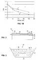
- FIG. 1Ais a plot illustrating the performance of a phosphor-converted light-emitting device as a function of the volume fraction of approximately 5 micron phosphor particles in a resin.
- FIG. 1Bis a plot illustrating the performance of resin encapsulated light-emitting diodes as a function of the weight % of non-absorbing scattering particles dispersed in the resin.
- FIG. 2is a schematic diagram of a light-emitting diode employed in some embodiments.
- FIG. 3is a schematic diagram of a light-emitting device in which nanoparticles are dispersed in a material disposed around a light-emitting semiconductor device in accordance with some embodiments.
- FIG. 4is a schematic diagram of a light-emitting device in which nanoparticles are dispersed in a layer of material disposed on a light-emitting semiconductor device in accordance with some embodiments.
- FIG. 5is a schematic diagram of a light-emitting device in which nanoparticles are dispersed in a material shaped as a lens in accordance with some embodiments.
- FIG. 6is a schematic diagram of a light-emitting device in which nanoparticles are dispersed in a layer of material that attaches an optical element to a light-emitting semiconductor device in accordance with some embodiments.
- FIG. 7is an exploded view of a light-emitting device incorporated into a package in accordance with some embodiments.
- nanoparticlerefers to a particle having a diameter (or similar cross-sectional dimension) typically much less than about one micron.
- Such nanoparticlesmay be of any shape and may comprise, for example, crystalline or amorphous solids or liquids.
- the inventorshave discovered that the efficiency of conventional phosphor-converted light-emitting devices is significantly decreased by scattering by the phosphor particles of both the primary emission from the semiconductor device and the secondary emission from the phosphor particles. A portion of the light scattered by the phosphor particles is scattered onto absorbing parts of the semiconductor device or its package and thereby lost.
- Such scattering by the phosphor particlesoccurs because they are typically substantially larger than the wavelengths of the primary and secondary emitted light, and because the phosphor particles typically have refractive indices at these wavelengths that are much larger than the surrounding medium.
- conventional phosphor converted light-emitting devicestypically utilize phosphor particles having diameters of about 2 microns ( ⁇ m) to about 20 ⁇ m.
- visible lightis conventionally defined to include wavelengths from about 380 nanometers (nm) to about 770 nm.
- Such conventional phosphor particleswhich typically have indices of refraction of about 1.7 to about 2.3 for visible light, are typically embedded in an epoxy or silicone host material having an index of refraction of about 1.5 at these wavelengths.
- FIG. 1AThe effect of such scattering on the efficiency of phosphor converted light-emitting semiconductor devices is shown, for example, in the plot in FIG. 1A .
- blue emission from a III-Nitride light-emitting diode (LED)is converted to green light by europium-doped strontium thiogallate phosphor particles (having diameters of about 4 ⁇ m to about 5 ⁇ m) dispersed in a silicone resin disposed on the LED.
- the horizontal axis of the plotlabeled “blue fraction,” represents the percentage of the blue light emitted by the LED that is unabsorbed and unconverted and hence present in the total light output of the phosphor-converted device.
- the horizontal axisalso represents the phosphor loading in the resin, with the phosphor loading decreasing along the axis from left to right.
- the left vertical axis of the plotrepresents the total light output, in lumens (lm), of the phosphor converted device.
- the right vertical axis, labeled “package gain,”represents a scaling factor by which a theoretical prediction of the total light output, based on the known characteristics of the LED and of the phosphor and neglecting scattering, must be multiplied to match the measured performance of the phosphor converted devices.
- An ideal devicewould have a “package gain” of one.
- the right vertical axismeasures the degree to which scattering by the phosphor particles has degraded the performance of the device.
- lower values of “package gain”indicate increased losses due to scattering.
- Diamond shaped data points 2indicate the relationship between the phosphor loading and the total light output.
- Square shaped data points 4similarly indicate the relationship between the phosphor loading and losses due to scattering by the phosphor particles.
- the inventorshave determined from the data shown in FIG. 1A and from the results of similar measurements that in conventional phosphor converted light-emitting devices losses due to scattering by large phosphor particles embedded in a lower refractive index host material increase as the volume fraction of the particles in the host material increases. From similar measurements the inventors have also determined that losses due to scattering also increase if the refractive index of the phosphor particles is increased and the volume fraction of phosphor particles and the type of host material is unchanged. Typically, about 50% of the total light power of a conventional phosphor-converted light-emitting device is lost due to scattering by the phosphor particles followed by absorption.
- FIG. 1Bplots normalized blue emission from III-Nitride LEDs encapsulated in silicone resin (vertical axis) versus the weight % of non-absorbing scattering particles dispersed in the resin.
- Curve 3represents devices in which the non-absorbing particles were approximately 5 ⁇ m BaSO 4 particles.
- Curve 5represents devices in which the non-absorbing particles were approximately 2 ⁇ m YOS particles. Blue emission decreases rapidly with increasing particle loading in the encapsulant for both sets of devices.
- the inventorshave recognized that scattering by phosphor particles of primary emission from a semiconductor device and of secondary emission from the phosphor particles themselves may be reduced by reducing the size of the phosphor particles to substantially below wavelengths (e.g., peak wavelengths) of the primary and secondary emission.
- wavelengthse.g., peak wavelengths
- semiconductor nanocrystals or semiconductor quantum dotswhich typically have a diameter less than about 10 nm and hence scatter little of the primary and secondary light, may be used as substantially non-scattering phosphors.
- the use of semiconductor nanocrystals and quantum dots to phosphor convert the output of a light-emitting semiconductor deviceis disclosed in U.S. Pat. No. 6,501,091 and in U.S. Pat. No.
- the inventorshave also recognized that light scattering by phosphor particles in phosphor converted light-emitting devices may be reduced by increasing the refractive index of the medium in which they are embedded to more closely match the refractive index of the phosphor particles.
- the desired increase in refractive index of the medium surrounding the phosphor particlesmay be accomplished by dispersing nanoparticles that are smaller than wavelengths (e.g., peak wavelengths) of the primary and secondary emission into the host material in which the phosphor particles are embedded.
- the nanoparticlesare chosen to have a refractive index greater than that of the host material. Due to their size, however, the nanoparticles scatter little of the emitted light.
- n⁇ i ⁇ ⁇ v i ⁇ n i ⁇ i ⁇ ⁇ v i ( 1 )
- equation (1)indicates that the refractive index of the mixture varies from about 1.5 to about 1.8 as the volume fraction of the nanoparticles in the mixture varies from about 0 to about 0.35.
- the upper limit on the refractive index of such a mixtureis set by the dispersability of the nanoparticles in the host material as well as by the refractive indices of the nanoparticles and of the host material.
- cerium oxide and titanium oxide nanoparticlesmay be dispersed in silicone to volume fractions exceeding about 30% to about 40%.
- the refractive index of such a mixturemay be adjusted such that, for example, conventional doped yttrium aluminum garnet (YAG) phosphor particles, which typically have an index of refraction of about 1.8, would not substantially scatter light if dispersed in the mixture.
- YAGyttrium aluminum garnet
- light extraction from a light-emitting semiconductor devicemay be increased by dispersing nanoparticles that are smaller than a wavelength (e.g., peak wavelength) of the light emitted by the device into a host material and disposing the mixture on or around the light-emitting semiconductor device.
- the nanoparticlesare chosen to have a refractive index greater than that of the host material. Light extraction is increased compared to that for a similar semiconductor light-emitting device encapsulated in only the host material because the increased refractive index of the mixture reduces losses due to total internal reflection.
- the inventorshave discovered that light extraction from phosphor particles dispersed in a host material can be increased by also dispersing in the host material nanoparticles that are smaller than a wavelength (e.g., a peak wavelength) of the light emitted by the phosphor particles.
- the nanoparticlesare chosen to have an index of refraction greater than that of the host material.
- Light extraction from the phosphor particlesis increased compared to that for phosphor materials dispersed in only the host material because of the increased refractive index of the surrounding medium.
- the inventorsexpect light extraction from phosphor particles having diameters less than about a wavelength (e.g., a peak wavelength) of the light emitted by the phosphor particles to increase as the concentration of the particles in the host material is increased.
- Suitable light-emitting semiconductor devicesthat may be used in combination with nanoparticles in accordance with embodiments of the present invention include, but are not limited to, devices formed from III-Nitrides, III-Phosphides, III-Arsenides, and combinations thereof. These devices may be, for example, light-emitting diodes or laser diodes and may emit light at ultraviolet, visible, or infrared wavelengths. Suitable light-emitting semiconductor devices are disclosed, for example, in U.S. Pat. No. 6,133,589, U.S. Pat. No. 6,229,160, and U.S. Pat. No. 6,486,499, all three of which are incorporated herein by reference in their entirety.
- LED 10may employ Al x In y Ga z N based LED 10 .
- LED 10includes a multilayered epitaxial structure 12 disposed on a buffer layer 14 , which in turn is disposed on substrate 16 .
- Substrate 16may be formed, for example, from sapphire (Al 2 O 3 ), silicon carbide, or a III-Nitride material.
- Epitaxial structure 12includes active region 18 disposed between p-type upper Al x In y Ga z N region 20 and lower Al x In y Ga z N region 22 .
- Al x In y Ga z N region 22includes n-type and/or undoped Al x In y Ga z N layers.
- Active region 18includes one or more quantum wells formed from layers of Al x In y Ga z N.
- Ohmic p-contact 24 and metallic layer 26are electrically coupled to each other and to upper Al x In y Ga z N region 20 .
- Ohmic n-contact 28is electrically coupled to lower Al x In y Ga z N region 22 .
- Application of a suitable forward bias across contacts 24 and 28results in injection of electrons and holes into active region 18 . Radiative recombination of electrons and holes in active region 18 generates light.
- metallic layer 26is semitransparent to light emitted by active region 18 .
- metallic layer 26is highly reflective to light emitted by active region 18 , and LED 10 is mounted as a flip-chip with contacts 24 and 28 facing a submount. It should be understood that the composition of Al x In y Ga z N may vary between the various layers and regions in LED 10 .
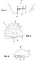
- a light-emitting device 30includes a light-emitting semiconductor device 32 disposed in a reflective cup 34 .
- Reflective cup 34also contains a material 36 that is substantially transparent to light emitted by device 32 .
- Nanoparticles 38 having an index of refraction greater than that of material 36 at wavelengths of light emitted by device 32are dispersed in substantially transparent material 36 .
- Nanoparticles 38are selected to have diameters less than about a wavelength (e.g., a peak wavelength) of light emitted by device 32 and hence do not substantially scatter the emitted light. 1
- nanoparticles 38have diameters less than about 1 ⁇ 4 of a peak emission wavelength of device 32 .
- nanoparticles 38have diameters of about 2 nm to about 50 nm and device 32 emits light having wavelengths greater than about 400 nm.
- Reflective cup 34reflects light emitted by light-emitting semiconductor device 32 to form an optical output of light-emitting device 30 .
- optional phosphor particles 40 shown in FIG. 3are also dispersed in material 36 .
- substantially transparentis used herein to indicate that a material so described transmits light at a peak wavelength emitted by device 32 with less than about 25%, preferably less than about 10%, more preferably less than about 2%, single pass loss due to absorption or scattering.
- Material 36may be organic or inorganic and may comprise, for example, materials including but not limited to conventional epoxies, acrylic polymers, polycarbonates, silicone polymers, optical glasses, chalcogenide glasses, spiro compounds, and mixtures thereof.
- nanoparticles 38do not substantially absorb light at wavelengths emitted by device 32 , particularly at peak emission wavelengths.
- the phrases “not substantially absorb” and “not substantially absorbing”are used herein to indicate that the nanoparticles in such implementations are sufficiently non-absorbing that they do not increase the single pass loss of light transmitted by the encapsulant to more than about 30%, preferably not to more than about 20%.
- the loss due to absorption by the nanoparticles of light emitted by device 32will depend on the absorption cross-sections of the individual nanoparticles, the concentration of the nanoparticles in substantially transparent material 36 , and possibly on interactions between the nanoparticles and the surrounding material.
- Suitable nanoparticles for such implementationsmay include, but are not limited to, nanoparticles of metal oxides, nitrides, nitridosilicates, and mixtures thereof.
- Suitable metal oxidesmay include, but are not limited to, calcium oxide, cerium oxide, hafnium oxide, titanium oxide, zinc oxide, zirconium oxide, and combinations thereof. Nanoparticles of such metal oxides having sizes ranging, for example, from about 2 nm to about 10 nm are available, for example, from Degussa-Huls AG of Frankfurt/Main Germany.
- Suitable nanoparticles for such implementationsmay also include nanoparticles of II–VI semiconductors such as zinc sulfide, zinc selenide, cadmium sulfide, cadmium selenide, cadmium telluride, and their ternary or quaternary mixtures, and nanoparticles of III–V semiconductors such as III-nitrides, III-phosphides, and mixtures thereof.
- Such semiconductor nanoparticleshave size tunable absorption spectra, as disclosed, for example, in U.S. Pat. No. 6,501,091 and in U.S. Pat. No. 6,803,719.
- the sizes of the semiconductor nanoparticlesmay be chosen such that the nanoparticles do not substantially absorb at wavelengths emitted by device 32 .
- nanoparticles 38absorb at least a portion of the primary light emitted by light-emitting semiconductor device 32 and emit secondary light of either longer or shorter wavelength than the absorbed light.
- nanoparticles 38act as phosphors.
- Suitable nanoparticles for such implementationsmay include, but are not limited to, nanoparticles of the II–VI and III–V materials listed above with sizes chosen such that the nanoparticles absorb a portion of the primary light.
- nanoparticles 38may be dispersed in material 36 with conventional mixing techniques used in fabricating conventional phosphor converted light-emitting devices and well known to one of ordinary skill in the art.
- a conventional three roll millmay be used to disperse nanoparticles in a silicone material.
- nanoparticlesmay be dispersed in chalcogenide and optical glasses, for example, by heating the glass to a molten state, adding the nanoparticles as a powder, and stirring the mixture using methods conventional in the glass making arts.
- some semiconductor nanoparticlesmay be grown or synthesized in a glass by conventional glass-making techniques used in the fabrication of color glass filters.
- the volume fraction (concentration) of nanoparticles 38 in material 36may be chosen in some implementations such that nanoparticles 38 together with material 36 provide a medium having a particular refractive index.
- the approximate volume fraction of nanoparticles 38 in material 36 needed to provide a desired refractive indexmay be determined using effective medium theory as explained above.
- the volume fraction of nanoparticles 38 in material 36may then be varied around the calculated value to determine the volume fraction that provides a mixture having the particular desired refractive index.
- the volume fraction of nanoparticles 38 in material 36may vary from about 20% to about 60%.
- nanoparticles 38 together with material 36may provide a medium having a refractive index greater than about 1.6, preferably greater than about 1.8, at a peak wavelength of the primary emission from light-emitting semiconductor device 32 , for example.
- material 36 and nanoparticles 38may be disposed in reflective cup 34 by a variety of well known methods.
- Light extraction from light-emitting semiconductor device 32may be advantageously increased compared to that for a similar light-emitting device encapsulated in material 36 because the increased refractive index of the mixture of nanoparticles 38 and material 36 may decrease losses due to total internal reflection at the interfaces of device 32 and material 36 . This increase in light extraction from device 32 may be accomplished without increasing scattering of the emitted light.
- nanoparticles 38may advantageously phosphor convert all of or a portion of the primary emission from semiconductor light-emitting device 32 to provide a desired total emission from light-emitting device 30 .
- nanoparticles 38 and their volume fraction in material 36may be chosen by conventional methods used in fabricating phosphor converted light-emitting devices such that the emission from nanoparticles 38 combines with unabsorbed emission from device 32 to provide white light. If necessary, mixing of primary emission from device 32 and secondary emission from nanoparticles 38 may be facilitated, for example, by roughening a surface of any element of light-emitting device 30 .
- additional phosphor particles 40are dispersed in material 36 .
- phosphor particles 40have a refractive index greater than that of material 36 at wavelengths of light emitted by light-emitting semiconductor device 32 .
- Phosphor particles 40may be dispersed in material 36 in combination with nanoparticles 38 that do not substantially absorb light emitted by device 32 or in combination with nanoparticles 38 that absorb a portion of the light emitted by device 32 and emit secondary light.
- phosphor particles 40have diameters greater than about a wavelength (e.g., a peak wavelength) of light emitted by device 32 .
- Suitable phosphor particles for such implementationsinclude, but are not limited to, particles of materials comprising yttrium aluminum garnets, sulfur substituted gallates, unsubstituted gallates, sulfur substituted aluminates, unsubstituted aluminates, phosphates, silicates (nitridosilicates, for example), selenides, sulfides, and mixtures thereof. These materials may be doped with (activated by), for example, rare earth ions including but not limited to cerium and europium ions. Phosphor particles 40 may also comprise other conventional phosphor materials known to one of ordinary skill in the art.
- phosphor particles 40have diameters less than about a wavelength (e.g., a peak wavelength) of light emitted by light-emitting semiconductor device 32 .
- Suitable nanoparticles for such implementationsmay include, but are not limited to, nanoparticles of the II–VI and III–V materials listed above with sizes chosen such that the nanoparticles absorb a portion of the primary light.
- Phosphor particles 40may also be or include organic dye molecules.
- Phosphor particles 40may be dispersed in material 36 in combination with nanoparticles 38 by conventional techniques such as those described above. Phosphor particles 40 and their volume fraction in material 36 may be chosen by conventional methods used in fabricating phosphor converted light-emitting devices such that light-emitting device 30 provides a desired output emission spectrum such as, for example, white light.
- the increased refractive index of the mixture of nanoparticles 38 and material 36 compared to that of material 36 alonemay advantageously decrease light scattering by and increase light extraction from phosphor particles 40 .
- the refractive index of the mixtureapproaches that of phosphor particles 40 , light scattering by the phosphor particles decreases toward zero and light extraction from the phosphor particles is optimized.
- nanoparticles 38 and their volume fraction in material 36may be chosen such that nanoparticles 38 and material 36 together provide a medium having a refractive index at a wavelength (e.g. a peak wavelength) of emission from device 32 or from phosphor particles 40 that approximately matches the refractive index of phosphor particles 40 at the same wavelength.
- a wavelengthe.g. a peak wavelength
- the choice of nanoparticles 38 and their volume fraction in material 36may be guided by effective medium theory similarly to as explained above.
- the refractive index of a mixture of silicone and cerium oxide or titanium oxide nanoparticlesmay be adjusted as described above to match that of YAG based phosphor particles to within about 10% to about 2% or better.
- the refractive index of the mixture of nanoparticles 38 and material 36 or the size of phosphor particles 40may be adjusted so as to provide a desired amount of light scattering by phosphor particles 40 .
- the refractive index of the mixtureis adjusted so that light scattering by phosphor particles 40 is set to a minimum level needed to facilitate mixing of light emitted by light-emitting semiconductor device 32 , phosphor particles 40 , and (optionally) nanoparticles 38 .
- a light-emitting device 42includes a light-emitting semiconductor device 32 disposed in a reflective cup 34 , and a layer 44 of material 36 disposed on one or more surface of device 32 .
- Nanoparticles 38 and, optionally, phosphor particles 40are dispersed in material 36 .
- Material 36 , nanoparticles 38 , and phosphor particles 40may be provided, for example, in any of the combinations described above with respect to light-emitting device 30 ( FIG. 3 ).
- the incorporation of nanoparticles 38 into light-emitting device 42may provide any of the previously described advantages.
- Layer 44may be deposited, for example, by conventional spraying, screen printing, and dipping methods. In one implementation, layer 44 may be a conformal layer applied with a stenciling method described in U.S. Pat. No. 6,650,044 incorporated herein by reference in its entirety.
- material 36is formed into a lens (or other optical element) as shown or provided in, for example, a hollow shell shaped as a lens or other optical element and disposed around light-emitting device 32 .
- Material 36 , nanoparticles 38 , and (optional) phosphor particles 40may be provided, for example, in any of the combinations described above.
- Material 36may be formed into a lens or other shape using conventional encapsulation methods familiar to one of ordinary skill in the art.
- the lens shaped portion of light-emitting device 46reduces losses due to total internal reflection and, in combination with reflector 34 , forms an optical output of light-emitting device 46 .
- a lens or other optical element 50is attached to a light-emitting semiconductor device 32 with a layer 52 of material 36 .
- Nanoparticles 38 , and (optional) phosphor particles 40may be dispersed in material 36 , for example, in any of the combinations described above.
- material 36is a high refractive index glass having a relatively low melting point
- optical element 50is bonded to light-emitting semiconductor device 32 with layer 52 by a wafer-bonding method such as, for example, those disclosed in U.S. patent application Ser. No. 09/660,317, incorporated herein by reference in its entirety.
- optical element 50may be advantageously formed.
- Light extraction from light-emitting semiconductor device 32may be advantageously increased by forming optical element 50 from a material having a relatively high refractive index.
- FIG. 7is an exploded view of a packaged light-emitting device in accordance with some embodiments.
- Light emitting device 54which may be any of the light-emitting devices described herein or a light-emitting semiconductor device component of such a light-emitting device, is mounted directly or indirectly via a thermally conducting submount 56 to a heat-sinking slug 58 .
- Slug 58may include an optional reflector cup 60 , which may be in addition to or substitute for reflector 34 ( FIGS. 3–5 ).
- Slug 58is placed into an insert-molded leadframe 62 .
- Insert-molded leadframe 62is, for example, a filled plastic material molded around a metal frame that provides an electrical path to light-emitting device 54 .
- a lens 64 or other optical elementmay be added. Lens 64 may be in addition to or substitute for the lenses shown in FIGS. 5 and 6 .
- nanoparticlesmay be employed as described above to reduce scattering by phosphor particles of light provided by light sources other than light-emitting semiconductor devices, and to improve light extraction from such light-sources.
- Alternative light sourcesinclude, for example, lasers, conventional incandescent lamps, and fluorescent lamps.
- material 36 including nanoparticles 38 and (optionally) phosphor particles 40is shown in the figures as disposed directly on light-emitting semiconductor device 32 , in other embodiments material 36 may be spaced apart from device 32 .
- material 36may be spaced apart from device 32 by a transparent spacer layer as disclosed in U.S. Pat. No. 5,959,316, incorporated herein by reference in its entirety.
- FIGS. 3–5each include a reflector 34 , some other embodiments do not include such a reflector.
- lenses employed in several embodimentshave been illustrated as dome-shaped, such lenses may have other shapes or may be implemented, for example, with a microlens array.
Landscapes
- Led Device Packages (AREA)
- Led Devices (AREA)
Abstract
Description
Claims (15)
Priority Applications (1)
| Application Number | Priority Date | Filing Date | Title |
|---|---|---|---|
| US11/033,594US7083490B2 (en) | 2002-06-07 | 2005-01-11 | Light-emitting devices utilizing nanoparticles |
Applications Claiming Priority (2)
| Application Number | Priority Date | Filing Date | Title |
|---|---|---|---|
| US10/165,571US6870311B2 (en) | 2002-06-07 | 2002-06-07 | Light-emitting devices utilizing nanoparticles |
| US11/033,594US7083490B2 (en) | 2002-06-07 | 2005-01-11 | Light-emitting devices utilizing nanoparticles |
Related Parent Applications (1)
| Application Number | Title | Priority Date | Filing Date |
|---|---|---|---|
| US10/165,571DivisionUS6870311B2 (en) | 2002-06-07 | 2002-06-07 | Light-emitting devices utilizing nanoparticles |
Publications (2)
| Publication Number | Publication Date |
|---|---|
| US20050215164A1 US20050215164A1 (en) | 2005-09-29 |
| US7083490B2true US7083490B2 (en) | 2006-08-01 |
Family
ID=29549380
Family Applications (2)
| Application Number | Title | Priority Date | Filing Date |
|---|---|---|---|
| US10/165,571Expired - LifetimeUS6870311B2 (en) | 2002-06-07 | 2002-06-07 | Light-emitting devices utilizing nanoparticles |
| US11/033,594Expired - LifetimeUS7083490B2 (en) | 2002-06-07 | 2005-01-11 | Light-emitting devices utilizing nanoparticles |
Family Applications Before (1)
| Application Number | Title | Priority Date | Filing Date |
|---|---|---|---|
| US10/165,571Expired - LifetimeUS6870311B2 (en) | 2002-06-07 | 2002-06-07 | Light-emitting devices utilizing nanoparticles |
Country Status (6)
| Country | Link |
|---|---|
| US (2) | US6870311B2 (en) |
| EP (1) | EP1369935B1 (en) |
| JP (1) | JP4666891B2 (en) |
| AU (1) | AU2003232393A1 (en) |
| TW (1) | TWI307969B (en) |
| WO (1) | WO2003105242A1 (en) |
Cited By (40)
| Publication number | Priority date | Publication date | Assignee | Title |
|---|---|---|---|---|
| US20050152421A1 (en)* | 2003-11-18 | 2005-07-14 | Sharp Kabushiki Kaisha | Semiconductor laser device and illumination apparatus |
| US20060251919A1 (en)* | 2005-05-04 | 2006-11-09 | Xerox Corporation | Organic light emitting devices |
| US20060263628A1 (en)* | 2005-05-20 | 2006-11-23 | Xerox Corporation | Display device with metal-organic mixed layer anodes |
| US20060263593A1 (en)* | 2005-05-20 | 2006-11-23 | Xerox Corporation | Display devices with light absorbing metal nonoparticle layers |
| US20060263629A1 (en)* | 2005-05-20 | 2006-11-23 | Xerox Corporation | Intermediate electrodes for stacked OLEDs |
| US20060261731A1 (en)* | 2005-05-20 | 2006-11-23 | Xerox Corporation | Stacked oled structure |
| US20070087197A1 (en)* | 2005-05-16 | 2007-04-19 | Samsung Electro-Mechanics Co., Ltd. | Coated nano particle and electronic device using the same |
| US20070196657A1 (en)* | 2005-12-15 | 2007-08-23 | Cabot Corporation | Transparent polymer composites |
| US20080152933A1 (en)* | 2006-12-21 | 2008-06-26 | Sony Corporation | Curable resin material-fine particle composite material and method of producing the same, optical material, and light emitting device |
| US20080308825A1 (en)* | 2007-06-14 | 2008-12-18 | Cree, Inc. | Encapsulant with scatterer to tailor spatial emission pattern and color uniformity in light emitting diodes |
| WO2009026105A1 (en)* | 2007-08-17 | 2009-02-26 | Massachusetts Institute Of Technology | Light emitting material |
| US20090072254A1 (en)* | 2007-09-14 | 2009-03-19 | Cree, Inc. | Polarization doping in nitride based diodes |
| US20090085463A1 (en)* | 2007-09-28 | 2009-04-02 | General Electric Company | Thermo-optically functional compositions, systems and methods of making |
| US20090256166A1 (en)* | 2005-08-05 | 2009-10-15 | Susumu Koike | Semiconductor light-emitting device |
| US20090261358A1 (en)* | 2008-03-31 | 2009-10-22 | Cree, Inc. | Emission tuning methods and devices fabricated utilizing methods |
| US20090272996A1 (en)* | 2008-05-02 | 2009-11-05 | Cree, Inc. | Encapsulation for phosphor-converted white light emitting diode |
| US20100084962A1 (en)* | 2007-03-06 | 2010-04-08 | Merck Patent Gesellschaft | Luminophores made of doped garnet for pcleds |
| US20100097779A1 (en)* | 2008-10-21 | 2010-04-22 | Mitutoyo Corporation | High intensity pulsed light source configurations |
| US20100118511A1 (en)* | 2008-11-07 | 2010-05-13 | James Wegat | Lighting systems |
| US20100117997A1 (en)* | 2007-03-08 | 2010-05-13 | Haase Michael A | Array of luminescent elements |
| CN101414651B (en)* | 2007-10-17 | 2010-06-16 | 洪绢欲 | Light emitting diode assembly with high refractive index nano-particle stacking device and method for manufacturing the same |
| US20100177496A1 (en)* | 2008-11-25 | 2010-07-15 | Jennifer Gillies | Custom color led replacements for traditional lighting fixtures |
| US7777407B2 (en) | 2005-05-04 | 2010-08-17 | Lg Display Co., Ltd. | Organic light emitting devices comprising a doped triazine electron transport layer |
| US20100208486A1 (en)* | 2008-10-21 | 2010-08-19 | Mitutoyo Corporation | High intensity pulsed light source configurations |
| US7795806B2 (en) | 2005-05-20 | 2010-09-14 | Lg Display Co., Ltd. | Reduced reflectance display devices containing a thin-layer metal-organic mixed layer (MOML) |
| US20110006321A1 (en)* | 2009-07-09 | 2011-01-13 | Samsung Electronics Co., Ltd | Composition for light emitting body-polymer composite, light emitting body-polymer composite, and light emitting device including the light emitting body-polymer composite |
| US20110140083A1 (en)* | 2009-12-16 | 2011-06-16 | Daniel Carleton Driscoll | Semiconductor Device Structures with Modulated Doping and Related Methods |
| US20110169030A1 (en)* | 2004-07-02 | 2011-07-14 | Cree, Inc. | Light emitting diode with high aspect ratio submicron roughness for light extraction and methods of forming |
| US20110186877A1 (en)* | 2008-06-05 | 2011-08-04 | Haase Michael A | Light emitting diode with bonded semiconductor wavelength converter |
| US20110278536A1 (en)* | 2010-05-17 | 2011-11-17 | Massachusetts Institute Of Technology | Light emitting material |
| DE102011077847A1 (en) | 2010-06-24 | 2011-12-29 | Mitutoyo Corp. | Radical phosphor configuration for a high intensity point source |
| EP2469241A2 (en) | 2010-12-27 | 2012-06-27 | Mitutoyo Corporation | Optical encoder readhead configuration |
| US20120195340A1 (en)* | 2006-05-11 | 2012-08-02 | Kwang-Ohk Cheon | Solid state lighting devices comprising quantum dots |
| US8317347B2 (en) | 2010-12-22 | 2012-11-27 | Mitutoyo Corporation | High intensity point source system for high spectral stability |
| US8415692B2 (en) | 2009-07-06 | 2013-04-09 | Cree, Inc. | LED packages with scattering particle regions |
| US8487331B2 (en) | 2010-03-31 | 2013-07-16 | Samsung Electronics Co., Ltd. | Liquid crystal display device including white light emitting diode |
| US8536615B1 (en) | 2009-12-16 | 2013-09-17 | Cree, Inc. | Semiconductor device structures with modulated and delta doping and related methods |
| US20130341590A1 (en)* | 2012-06-25 | 2013-12-26 | Cree, Inc. | Quantum Dot Narrow-Band Downconverters for High Efficiency LEDs |
| US9012937B2 (en) | 2007-10-10 | 2015-04-21 | Cree, Inc. | Multiple conversion material light emitting diode package and method of fabricating same |
| US11313671B2 (en) | 2019-05-28 | 2022-04-26 | Mitutoyo Corporation | Chromatic confocal range sensing system with enhanced spectrum light source configuration |
Families Citing this family (210)
| Publication number | Priority date | Publication date | Assignee | Title |
|---|---|---|---|---|
| US7053419B1 (en) | 2000-09-12 | 2006-05-30 | Lumileds Lighting U.S., Llc | Light emitting diodes with improved light extraction efficiency |
| JP2002141556A (en) | 2000-09-12 | 2002-05-17 | Lumileds Lighting Us Llc | Light-emitting diode with improved light extraction effect |
| US6744077B2 (en)* | 2002-09-27 | 2004-06-01 | Lumileds Lighting U.S., Llc | Selective filtering of wavelength-converted semiconductor light emitting devices |
| US8993221B2 (en) | 2012-02-10 | 2015-03-31 | Pixelligent Technologies, Llc | Block co-polymer photoresist |
| US7524616B2 (en) | 2003-03-04 | 2009-04-28 | Pixelligent Technologies Llc | Applications of semiconductor nano-sized particles for photolithography |
| US7279832B2 (en)* | 2003-04-01 | 2007-10-09 | Innovalight, Inc. | Phosphor materials and illumination devices made therefrom |
| US20040252488A1 (en)* | 2003-04-01 | 2004-12-16 | Innovalight | Light-emitting ceiling tile |
| US20070013057A1 (en)* | 2003-05-05 | 2007-01-18 | Joseph Mazzochette | Multicolor LED assembly with improved color mixing |
| US7193784B2 (en)* | 2003-05-20 | 2007-03-20 | Kansas State University Research Foundation | Nitride microlens |
| AU2003302306A1 (en)* | 2003-06-13 | 2005-01-28 | Ers Company | Moisture-resistant nano-particle material and its applications |
| DE10361661A1 (en)* | 2003-07-14 | 2005-03-17 | Osram Opto Semiconductors Gmbh | Light-emitting component has luminescence conversion element, filter element with nano-particles that selectively reduce radiation intensity of unwanted radiation spectral sub-region(s) by absorption |
| US7009213B2 (en)* | 2003-07-31 | 2006-03-07 | Lumileds Lighting U.S., Llc | Light emitting devices with improved light extraction efficiency |
| JP2005064233A (en)* | 2003-08-12 | 2005-03-10 | Stanley Electric Co Ltd | Wavelength conversion type LED |
| JP2005093712A (en)* | 2003-09-17 | 2005-04-07 | Stanley Electric Co Ltd | Semiconductor light emitting device |
| DE10345157B4 (en)* | 2003-09-29 | 2009-01-08 | Qimonda Ag | Thermally conductive packaging of electronic circuit units |
| TW200517437A (en)* | 2003-10-16 | 2005-06-01 | Nitto Denko Corp | Epoxy resin composition for encapsulating optical semiconductor element and optical semiconductor device using the same |
| US20070212542A1 (en)* | 2003-10-22 | 2007-09-13 | The Regents Of The University Of California | Methods for Preparing and Functionalizing Nanoparticles |
| DE10351397A1 (en)* | 2003-10-31 | 2005-06-16 | Osram Opto Semiconductors Gmbh | LED chip |
| DE10351349A1 (en) | 2003-10-31 | 2005-06-16 | Osram Opto Semiconductors Gmbh | Production of a luminescent diode chip applies a radiation decoupling surface and a semiconductor body with an epitaxial-grown sequence of semiconductor layers with an active zone |
| JP4590905B2 (en)* | 2003-10-31 | 2010-12-01 | 豊田合成株式会社 | Light emitting element and light emitting device |
| US7102152B2 (en)* | 2004-10-14 | 2006-09-05 | Avago Technologies Ecbu Ip (Singapore) Pte. Ltd. | Device and method for emitting output light using quantum dots and non-quantum fluorescent material |
| US7318651B2 (en) | 2003-12-18 | 2008-01-15 | Avago Technologies Ecbu Ip (Singapore) Pte. Ltd. | Flash module with quantum dot light conversion |
| US7667766B2 (en) | 2003-12-18 | 2010-02-23 | Avago Technologies Ecbu Ip (Singapore) Pte. Ltd. | Adjustable spectrum flash lighting for image acquisition |
| TWI236162B (en)* | 2003-12-26 | 2005-07-11 | Ind Tech Res Inst | Light emitting diode |
| JP4231418B2 (en)* | 2004-01-07 | 2009-02-25 | 株式会社小糸製作所 | Light emitting module and vehicle lamp |
| US7645397B2 (en) | 2004-01-15 | 2010-01-12 | Nanosys, Inc. | Nanocrystal doped matrixes |
| WO2005067524A2 (en)* | 2004-01-15 | 2005-07-28 | Nanosys, Inc. | Nanocrystal doped matrixes |
| US20050269932A1 (en)* | 2004-01-21 | 2005-12-08 | Ng Kee Y | Apparatus, device and method for emitting output light using group IIB element selenide-based phosphor material and/or thiogallate-based phosphor material |
| US20050156510A1 (en)* | 2004-01-21 | 2005-07-21 | Chua Janet B.Y. | Device and method for emitting output light using group IIB element selenide-based and group IIA element gallium sulfide-based phosphor materials |
| US20050167684A1 (en)* | 2004-01-21 | 2005-08-04 | Chua Janet B.Y. | Device and method for emitting output light using group IIB element selenide-based phosphor material |
| CN100446279C (en)* | 2004-02-18 | 2008-12-24 | 财团法人工业技术研究院 | Light emitting diode |
| US7868343B2 (en) | 2004-04-06 | 2011-01-11 | Cree, Inc. | Light-emitting devices having multiple encapsulation layers with at least one of the encapsulation layers including nanoparticles and methods of forming the same |
| US7553683B2 (en)* | 2004-06-09 | 2009-06-30 | Philips Lumiled Lighting Co., Llc | Method of forming pre-fabricated wavelength converting elements for semiconductor light emitting devices |
| US20060006397A1 (en)* | 2004-07-09 | 2006-01-12 | Chua Janet B Y | Device and method for emitting output light using group IIA/IIB selenide sulfur-based phosphor material |
| US7750352B2 (en) | 2004-08-10 | 2010-07-06 | Pinion Technologies, Inc. | Light strips for lighting and backlighting applications |
| JP4786886B2 (en)* | 2004-08-11 | 2011-10-05 | ローム株式会社 | Semiconductor light emitting device |
| US7471040B2 (en)* | 2004-08-13 | 2008-12-30 | Avago Technologies Ecbu Ip (Singapore) Pte. Ltd. | Mixed-color light emitting diode apparatus, and method for making same |
| KR100668609B1 (en)* | 2004-09-24 | 2007-01-16 | 엘지전자 주식회사 | White light source element |
| TWI256149B (en)* | 2004-09-27 | 2006-06-01 | Advanced Optoelectronic Tech | Light apparatus having adjustable color light and manufacturing method thereof |
| US7265488B2 (en)* | 2004-09-30 | 2007-09-04 | Avago Technologies General Ip Pte. Ltd | Light source with wavelength converting material |
| CN101040397B (en)* | 2004-10-12 | 2010-12-08 | 皇家飞利浦电子股份有限公司 | Electroluminescent light source |
| US8816369B2 (en) | 2004-10-29 | 2014-08-26 | Led Engin, Inc. | LED packages with mushroom shaped lenses and methods of manufacturing LED light-emitting devices |
| US7304425B2 (en)* | 2004-10-29 | 2007-12-04 | 3M Innovative Properties Company | High brightness LED package with compound optical element(s) |
| US20060091414A1 (en)* | 2004-10-29 | 2006-05-04 | Ouderkirk Andrew J | LED package with front surface heat extractor |
| US8324641B2 (en)* | 2007-06-29 | 2012-12-04 | Ledengin, Inc. | Matrix material including an embedded dispersion of beads for a light-emitting device |
| US8134292B2 (en)* | 2004-10-29 | 2012-03-13 | Ledengin, Inc. | Light emitting device with a thermal insulating and refractive index matching material |
| US9929326B2 (en) | 2004-10-29 | 2018-03-27 | Ledengin, Inc. | LED package having mushroom-shaped lens with volume diffuser |
| US7419839B2 (en) | 2004-11-12 | 2008-09-02 | Philips Lumileds Lighting Company, Llc | Bonding an optical element to a light emitting device |
| US7462502B2 (en)* | 2004-11-12 | 2008-12-09 | Philips Lumileds Lighting Company, Llc | Color control by alteration of wavelength converting element |
| WO2006054233A2 (en)* | 2004-11-19 | 2006-05-26 | Koninklijke Philips Electronics N.V. | Light-emitting device with inorganic housing |
| WO2006061729A2 (en)* | 2004-12-06 | 2006-06-15 | Philips Intellectual Property & Standards Gmbh | Organic electroluminescent light source |
| ATE527705T1 (en)* | 2004-12-06 | 2011-10-15 | Koninkl Philips Electronics Nv | ORGANIC ELECTROLUMINescent LIGHT SOURCE |
| US7602116B2 (en)* | 2005-01-27 | 2009-10-13 | Advanced Optoelectronic Technology, Inc. | Light apparatus capable of emitting light of multiple wavelengths using nanometer fluorescent material, light device and manufacturing method thereof |
| US7522211B2 (en) | 2005-02-10 | 2009-04-21 | Avago Technologies Ecbu Ip (Singapore) Pte. Ltd. | Studio light |
| US7341878B2 (en)* | 2005-03-14 | 2008-03-11 | Philips Lumileds Lighting Company, Llc | Wavelength-converted semiconductor light emitting device |
| US7879258B2 (en) | 2005-03-14 | 2011-02-01 | Koninklijke Philips Electronics N.V. | Phosphor in polycrystalline ceramic structure and a light-emitting element comprising same |
| EP1864274B1 (en)* | 2005-03-25 | 2019-04-24 | Arkema France | Illuminating device combining a led and a diffusing sheet |
| JP2006310710A (en) | 2005-05-02 | 2006-11-09 | Sony Corp | Semiconductor light emitting device |
| KR100682874B1 (en)* | 2005-05-02 | 2007-02-15 | 삼성전기주식회사 | White LED |
| US7868302B2 (en)* | 2005-05-05 | 2011-01-11 | Board Of Regents Of The University Of Nebraska | Nano-particle/quantum dot based optical diode |
| DE102005023134A1 (en)* | 2005-05-19 | 2006-11-23 | Patent-Treuhand-Gesellschaft für elektrische Glühlampen mbH | Luminescence conversion LED |
| US9297092B2 (en) | 2005-06-05 | 2016-03-29 | Qd Vision, Inc. | Compositions, optical component, system including an optical component, devices, and other products |
| US8718437B2 (en) | 2006-03-07 | 2014-05-06 | Qd Vision, Inc. | Compositions, optical component, system including an optical component, devices, and other products |
| WO2007103310A2 (en) | 2006-03-07 | 2007-09-13 | Qd Vision, Inc. | An article including semiconductor nanocrystals |
| WO2006134982A1 (en)* | 2005-06-14 | 2006-12-21 | Denki Kagaku Kogyo Kabushiki Kaisha | Resin composition and sheet containing phosphor, and light emitting element using such composition and sheet |
| DE102005061828B4 (en)* | 2005-06-23 | 2017-05-24 | Osram Opto Semiconductors Gmbh | Wavelength-converting converter material, light-emitting optical component and method for its production |
| CA2597697C (en)* | 2005-06-23 | 2014-12-02 | Rensselaer Polytechnic Institute | Package design for producing white light with short-wavelength leds and down-conversion materials |
| KR101161383B1 (en) | 2005-07-04 | 2012-07-02 | 서울반도체 주식회사 | Light emitting diode and method for producing the same |
| KR101106134B1 (en)* | 2005-07-11 | 2012-01-20 | 서울옵토디바이스주식회사 | Light Emitting Diode Adopting Nanowire Phosphor |
| JP5066084B2 (en)* | 2005-07-14 | 2012-11-07 | コーニンクレッカ フィリップス エレクトロニクス エヌ ヴィ | Electroluminescence device |
| JP4778745B2 (en)* | 2005-07-27 | 2011-09-21 | パナソニック株式会社 | Semiconductor light emitting device and manufacturing method thereof |
| US20070023762A1 (en)* | 2005-07-29 | 2007-02-01 | Luxo Asa And Oec Ag | White light emitting LED-powered lamp |
| US8187726B2 (en)* | 2005-08-09 | 2012-05-29 | Sony Corporation | Nanoparticle-resin composite material, light emitting device assembly, and filling material for the light-emitting device assembly |
| JP2007053170A (en)* | 2005-08-16 | 2007-03-01 | Toshiba Corp | Light emitting device |
| JP4415972B2 (en)* | 2005-09-22 | 2010-02-17 | ソニー株式会社 | Method for producing metal oxide nanoparticles |
| US7594845B2 (en)* | 2005-10-20 | 2009-09-29 | 3M Innovative Properties Company | Abrasive article and method of modifying the surface of a workpiece |
| JP2007299981A (en)* | 2006-05-01 | 2007-11-15 | Sumitomo Osaka Cement Co Ltd | Light emitting element, sealing composition thereof, and optical semiconductor device |
| KR101302277B1 (en)* | 2005-10-28 | 2013-09-02 | 스미토모 오사카 세멘토 가부시키가이샤 | Transparent inorganic-oxide dispersion, resin composition containing inorganic oxide particles, composition for encapsulating luminescent element, luminescent element, hard coat, optical functional film, optical part, and process for producing resin composition containing inorganic oxide particles |
| US20070116423A1 (en)* | 2005-11-22 | 2007-05-24 | 3M Innovative Properties Company | Arrays of optical elements and method of manufacturing same |
| US7772604B2 (en) | 2006-01-05 | 2010-08-10 | Illumitex | Separate optical device for directing light from an LED |
| US7795625B2 (en) | 2006-01-16 | 2010-09-14 | Panasonic Corporation | Semiconductor light-emitting device |
| US8044412B2 (en) | 2006-01-20 | 2011-10-25 | Taiwan Semiconductor Manufacturing Company, Ltd | Package for a light emitting element |
| KR100867519B1 (en)* | 2006-02-02 | 2008-11-07 | 삼성전기주식회사 | Light emitting diode module |
| US9874674B2 (en) | 2006-03-07 | 2018-01-23 | Samsung Electronics Co., Ltd. | Compositions, optical component, system including an optical component, devices, and other products |
| US9951438B2 (en) | 2006-03-07 | 2018-04-24 | Samsung Electronics Co., Ltd. | Compositions, optical component, system including an optical component, devices, and other products |
| US8849087B2 (en)* | 2006-03-07 | 2014-09-30 | Qd Vision, Inc. | Compositions, optical component, system including an optical component, devices, and other products |
| JP2007277467A (en) | 2006-04-10 | 2007-10-25 | Sony Chemical & Information Device Corp | Curable resin composition |
| US8141384B2 (en)* | 2006-05-03 | 2012-03-27 | 3M Innovative Properties Company | Methods of making LED extractor arrays |
| US7423297B2 (en)* | 2006-05-03 | 2008-09-09 | 3M Innovative Properties Company | LED extractor composed of high index glass |
| CN101467266A (en)* | 2006-06-08 | 2009-06-24 | 皇家飞利浦电子股份有限公司 | Light emitting device |
| US7470974B2 (en)* | 2006-07-14 | 2008-12-30 | Cabot Corporation | Substantially transparent material for use with light-emitting device |
| KR100901947B1 (en)* | 2006-07-14 | 2009-06-10 | 삼성전자주식회사 | White light emitting diode using semiconductor nanocrystal and manufacturing method thereof |
| JP2010500747A (en)* | 2006-08-08 | 2010-01-07 | コーニンクレッカ フィリップス エレクトロニクス エヌ ヴィ | Nanoparticle-based inorganic binding materials |
| US20100224890A1 (en)* | 2006-09-18 | 2010-09-09 | Cree, Inc. | Light emitting diode chip with electrical insulation element |
| US20090275266A1 (en)* | 2006-10-02 | 2009-11-05 | Illumitex, Inc. | Optical device polishing |
| WO2008042351A2 (en)* | 2006-10-02 | 2008-04-10 | Illumitex, Inc. | Led system and method |
| TWI338380B (en)* | 2006-10-11 | 2011-03-01 | Chuan Yu Hung | Light emitting diode incorporating high refractive index material |
| JP4952906B2 (en) | 2006-11-15 | 2012-06-13 | ソニーケミカル&インフォメーションデバイス株式会社 | Encapsulating resin composition and light emitting device |
| WO2008063652A1 (en) | 2006-11-21 | 2008-05-29 | Qd Vision, Inc. | Blue emitting semiconductor nanocrystals and compositions and devices including same |
| WO2008063658A2 (en)* | 2006-11-21 | 2008-05-29 | Qd Vision, Inc. | Semiconductor nanocrystals and compositions and devices including same |
| JP2010512662A (en) | 2006-12-11 | 2010-04-22 | ザ リージェンツ オブ ザ ユニバーシティ オブ カリフォルニア | Transparent light emitting diode |
| WO2008079078A1 (en) | 2006-12-22 | 2008-07-03 | Qunano Ab | Elevated led and method of producing such |
| US8951632B2 (en) | 2007-01-03 | 2015-02-10 | Applied Nanostructured Solutions, Llc | CNT-infused carbon fiber materials and process therefor |
| US9005755B2 (en) | 2007-01-03 | 2015-04-14 | Applied Nanostructured Solutions, Llc | CNS-infused carbon nanomaterials and process therefor |
| US8951631B2 (en) | 2007-01-03 | 2015-02-10 | Applied Nanostructured Solutions, Llc | CNT-infused metal fiber materials and process therefor |
| US8836212B2 (en) | 2007-01-11 | 2014-09-16 | Qd Vision, Inc. | Light emissive printed article printed with quantum dot ink |
| US8021904B2 (en)* | 2007-02-01 | 2011-09-20 | Cree, Inc. | Ohmic contacts to nitrogen polarity GaN |
| ITTO20070099A1 (en)* | 2007-02-09 | 2008-08-10 | St Microelectronics Srl | PROCEDURE FOR THE REALIZATION OF AN INTERFACE BETWEEN SILICON CARBIDE AND SILICON OXIDE WITH LOW DENSITY OF STATES |
| US20100110728A1 (en) | 2007-03-19 | 2010-05-06 | Nanosys, Inc. | Light-emitting diode (led) devices comprising nanocrystals |
| CA2678798C (en)* | 2007-03-19 | 2017-06-20 | Nanosys, Inc. | Methods for encapsulating nanocrystals |
| US20100155749A1 (en)* | 2007-03-19 | 2010-06-24 | Nanosys, Inc. | Light-emitting diode (led) devices comprising nanocrystals |
| KR100900866B1 (en)* | 2007-05-09 | 2009-06-04 | 삼성전자주식회사 | Light Emitting Diode Device Using Nanocrystal-Metal Oxide Composite and Its Manufacturing Method |
| WO2009014590A2 (en) | 2007-06-25 | 2009-01-29 | Qd Vision, Inc. | Compositions and methods including depositing nanomaterial |
| TWI365546B (en)* | 2007-06-29 | 2012-06-01 | Ind Tech Res Inst | Light emitting diode device and fabrication method thereof |
| WO2009014707A2 (en) | 2007-07-23 | 2009-01-29 | Qd Vision, Inc. | Quantum dot light enhancement substrate and lighting device including same |
| US11114594B2 (en)* | 2007-08-24 | 2021-09-07 | Creeled, Inc. | Light emitting device packages using light scattering particles of different size |
| US8128249B2 (en) | 2007-08-28 | 2012-03-06 | Qd Vision, Inc. | Apparatus for selectively backlighting a material |
| US7791093B2 (en) | 2007-09-04 | 2010-09-07 | Koninklijke Philips Electronics N.V. | LED with particles in encapsulant for increased light extraction and non-yellow off-state color |
| DE102007049005A1 (en)* | 2007-09-11 | 2009-03-12 | Osram Opto Semiconductors Gmbh | Radiating device, especially a light-emitting diode, has a layer emitting primary radiation and a conversion layer comprising two materials which convert this radiation into first and second secondary radiation |
| US7446159B1 (en) | 2007-09-20 | 2008-11-04 | Sony Corporation | Curable resin composition |
| DE602007007216D1 (en)* | 2007-09-25 | 2010-07-29 | Sony Chem & Inf Device Corp | Crosslinkable resin composition |
| US8368100B2 (en)* | 2007-11-14 | 2013-02-05 | Cree, Inc. | Semiconductor light emitting diodes having reflective structures and methods of fabricating same |
| US8294156B2 (en)* | 2007-11-19 | 2012-10-23 | Samsung Electronics Co., Ltd. | Nanocrystal light-emitting diode |
| EP2216834B1 (en) | 2007-11-29 | 2017-03-15 | Nichia Corporation | Light-emitting apparatus |
| US20090154198A1 (en)* | 2007-12-14 | 2009-06-18 | Joo Hoon Lee | Reflection type display apparatus |
| US9431589B2 (en)* | 2007-12-14 | 2016-08-30 | Cree, Inc. | Textured encapsulant surface in LED packages |
| US20090173958A1 (en)* | 2008-01-04 | 2009-07-09 | Cree, Inc. | Light emitting devices with high efficiency phospor structures |
| JP2011512037A (en)* | 2008-02-08 | 2011-04-14 | イルミテックス, インコーポレイテッド | System and method for emitter layer shaping |
| WO2009105581A1 (en)* | 2008-02-21 | 2009-08-27 | Nitto Denko Corporation | Light emitting device with translucent ceramic plate |
| WO2009145813A1 (en) | 2008-03-04 | 2009-12-03 | Qd Vision, Inc. | Particles including nanoparticles, uses thereof, and methods |
| CN102057491B (en)* | 2008-04-03 | 2012-11-21 | 班德加普工程有限公司 | Designing the host of nano-structured optoelectronic devices to improve performance |
| DE102008021438A1 (en)* | 2008-04-29 | 2009-12-31 | Schott Ag | Conversion material in particular for a, a semiconductor light source comprising white or colored light source, method for its preparation and this conversion material comprising light source |
| WO2009151515A1 (en) | 2008-05-06 | 2009-12-17 | Qd Vision, Inc. | Solid state lighting devices including quantum confined semiconductor nanoparticles |
| US9207385B2 (en) | 2008-05-06 | 2015-12-08 | Qd Vision, Inc. | Lighting systems and devices including same |
| WO2009137053A1 (en) | 2008-05-06 | 2009-11-12 | Qd Vision, Inc. | Optical components, systems including an optical component, and devices |
| EP2301071B1 (en) | 2008-05-29 | 2019-05-08 | Cree, Inc. | Light source with near field mixing |
| US8383432B2 (en)* | 2008-08-07 | 2013-02-26 | Sharp Laboratories Of America, Inc. | Colloidal-processed silicon particle device |
| US7888691B2 (en)* | 2008-08-29 | 2011-02-15 | Koninklijke Philips Electronics N.V. | Light source including a wavelength-converted semiconductor light emitting device and a filter |
| JP2012504860A (en)* | 2008-10-01 | 2012-02-23 | コーニンクレッカ フィリップス エレクトロニクス エヌ ヴィ | LED with particles in encapsulant for increased light extraction and non-yellow off-state color |
| US8075165B2 (en)* | 2008-10-14 | 2011-12-13 | Ledengin, Inc. | Total internal reflection lens and mechanical retention and locating device |
| US20100117106A1 (en)* | 2008-11-07 | 2010-05-13 | Ledengin, Inc. | Led with light-conversion layer |
| TW201034256A (en) | 2008-12-11 | 2010-09-16 | Illumitex Inc | Systems and methods for packaging light-emitting diode devices |
| US8507300B2 (en)* | 2008-12-24 | 2013-08-13 | Ledengin, Inc. | Light-emitting diode with light-conversion layer |
| US10214686B2 (en) | 2008-12-30 | 2019-02-26 | Nanosys, Inc. | Methods for encapsulating nanocrystals and resulting compositions |
| US11198270B2 (en) | 2008-12-30 | 2021-12-14 | Nanosys, Inc. | Quantum dot films, lighting devices, and lighting methods |
| US8343575B2 (en) | 2008-12-30 | 2013-01-01 | Nanosys, Inc. | Methods for encapsulating nanocrystals and resulting compositions |
| US8580342B2 (en) | 2009-02-27 | 2013-11-12 | Applied Nanostructured Solutions, Llc | Low temperature CNT growth using gas-preheat method |
| US20100227134A1 (en) | 2009-03-03 | 2010-09-09 | Lockheed Martin Corporation | Method for the prevention of nanoparticle agglomeration at high temperatures |
| US20100264371A1 (en)* | 2009-03-19 | 2010-10-21 | Nick Robert J | Composition including quantum dots, uses of the foregoing, and methods |
| US8598793B2 (en) | 2011-05-12 | 2013-12-03 | Ledengin, Inc. | Tuning of emitter with multiple LEDs to a single color bin |
| US7985000B2 (en)* | 2009-04-08 | 2011-07-26 | Ledengin, Inc. | Lighting apparatus having multiple light-emitting diodes with individual light-conversion layers |
| CN101894901B (en) | 2009-04-08 | 2013-11-20 | 硅谷光擎 | Package for multiple light emitting diodes |
| EP2424941B1 (en) | 2009-05-01 | 2017-05-31 | Nanosys, Inc. | Functionalized matrixes for dispersion of nanostructures |
| CN102470546B (en)* | 2009-08-03 | 2014-08-13 | 应用纳米结构方案公司 | Incorporation of nanoparticles in composite fibers |
| CN102598313B (en) | 2009-08-14 | 2016-03-23 | Qd视光有限公司 | Light emitting device, optical element for light emitting device, and method |
| US8585253B2 (en) | 2009-08-20 | 2013-11-19 | Illumitex, Inc. | System and method for color mixing lens array |
| US8449128B2 (en)* | 2009-08-20 | 2013-05-28 | Illumitex, Inc. | System and method for a lens and phosphor layer |
| WO2011031876A1 (en) | 2009-09-09 | 2011-03-17 | Qd Vision, Inc. | Formulations including nanoparticles |
| CN102482457B (en) | 2009-09-09 | 2015-04-15 | Qd视光有限公司 | Particles including nanoparticles, uses thereof, and methods |
| JP2013509714A (en)* | 2009-10-30 | 2013-03-14 | ナノシス・インク. | Light emitting diode (LED) device comprising nanocrystals |
| US8203161B2 (en) | 2009-11-23 | 2012-06-19 | Koninklijke Philips Electronics N.V. | Wavelength converted semiconductor light emitting device |
| US8303141B2 (en)* | 2009-12-17 | 2012-11-06 | Ledengin, Inc. | Total internal reflection lens with integrated lamp cover |
| JP2010098335A (en)* | 2010-02-01 | 2010-04-30 | Toshiba Corp | Light-emitting device |
| KR100969100B1 (en) | 2010-02-12 | 2010-07-09 | 엘지이노텍 주식회사 | Light emitting device, manufacturing method and light emitting device package |
| WO2011111293A1 (en) | 2010-03-10 | 2011-09-15 | パナソニック株式会社 | Led-packaging resin body, led device, and method for manufacturing led device |
| US8530883B2 (en)* | 2010-03-11 | 2013-09-10 | Light-Based Technologies Incorporated | Manufacture of quantum dot-enabled solid-state light emitters |
| US9080729B2 (en) | 2010-04-08 | 2015-07-14 | Ledengin, Inc. | Multiple-LED emitter for A-19 lamps |
| US9345095B2 (en) | 2010-04-08 | 2016-05-17 | Ledengin, Inc. | Tunable multi-LED emitter module |
| US8858022B2 (en) | 2011-05-05 | 2014-10-14 | Ledengin, Inc. | Spot TIR lens system for small high-power emitter |
| WO2012002780A2 (en)* | 2010-07-01 | 2012-01-05 | Samsung Electronics Co., Ltd. | Composition for light-emitting particle-polymer composite, light-emitting particle-polymer composite, and device including the light-emitting particle-polymer composite |
| US9382470B2 (en) | 2010-07-01 | 2016-07-05 | Samsung Electronics Co., Ltd. | Thiol containing compositions for preparing a composite, polymeric composites prepared therefrom, and articles including the same |
| CN102386317A (en)* | 2010-09-01 | 2012-03-21 | 富士康(昆山)电脑接插件有限公司 | Lead frame combination of light-emitting diode |
| KR101870844B1 (en) | 2010-09-14 | 2018-06-25 | 어플라이드 나노스트럭처드 솔루션스, 엘엘씨. | Glass substrates having carbon nanotubes grown thereon and methods for production thereof |
| BR112013005529A2 (en) | 2010-09-22 | 2016-05-03 | Applied Nanostructured Sols | carbon fiber substrates having carbon nanotubes developed therein, and processes for producing them |
| US9070851B2 (en) | 2010-09-24 | 2015-06-30 | Seoul Semiconductor Co., Ltd. | Wafer-level light emitting diode package and method of fabricating the same |
| JP5468517B2 (en)* | 2010-10-19 | 2014-04-09 | パナソニック株式会社 | Semiconductor light emitting device |
| KR102496406B1 (en) | 2010-11-10 | 2023-02-06 | 나노시스, 인크. | Quantum dot films, lighting devices, and lighting methods |
| RU2595711C2 (en)* | 2010-12-21 | 2016-08-27 | Конинклейке Филипс Электроникс Н.В. | Lighting device with polymer containing matrices |
| CN103384794B (en) | 2010-12-23 | 2018-05-29 | 三星电子株式会社 | Optical components containing quantum dots |
| US8513900B2 (en) | 2011-05-12 | 2013-08-20 | Ledengin, Inc. | Apparatus for tuning of emitter with multiple LEDs to a single color bin |
| US9134595B2 (en)* | 2011-09-29 | 2015-09-15 | Casio Computer Co., Ltd. | Phosphor device, illumination apparatus and projector apparatus |
| US9365766B2 (en)* | 2011-10-13 | 2016-06-14 | Intematix Corporation | Wavelength conversion component having photo-luminescence material embedded into a hermetic material for remote wavelength conversion |
| US9726928B2 (en) | 2011-12-09 | 2017-08-08 | Samsung Electronics Co., Ltd. | Backlight unit and liquid crystal display including the same |
| US11032884B2 (en) | 2012-03-02 | 2021-06-08 | Ledengin, Inc. | Method for making tunable multi-led emitter module |
| US9897284B2 (en) | 2012-03-28 | 2018-02-20 | Ledengin, Inc. | LED-based MR16 replacement lamp |
| JP2013232479A (en) | 2012-04-27 | 2013-11-14 | Toshiba Corp | Semiconductor light-emitting device |
| WO2013175773A1 (en)* | 2012-05-22 | 2013-11-28 | パナソニック株式会社 | Wavelength conversion element and method for manufacturing same, as well as led element and semiconductor laser emission device using wavelength conversion element |
| US9929325B2 (en) | 2012-06-05 | 2018-03-27 | Samsung Electronics Co., Ltd. | Lighting device including quantum dots |
| US9139770B2 (en) | 2012-06-22 | 2015-09-22 | Nanosys, Inc. | Silicone ligands for stabilizing quantum dot films |
| TWI596188B (en) | 2012-07-02 | 2017-08-21 | 奈米系統股份有限公司 | High-luminous nano structure and manufacturing method thereof |
| US20150171372A1 (en)* | 2012-07-04 | 2015-06-18 | Sharp Kabushiki Kaisha | Fluorescent material, fluorescent coating material, phosphor substrate, electronic apparatus, and led package |
| CN105247010B (en) | 2013-03-14 | 2017-10-24 | 纳米系统公司 | Solvent-free quantum dot exchange method |
| US9234801B2 (en) | 2013-03-15 | 2016-01-12 | Ledengin, Inc. | Manufacturing method for LED emitter with high color consistency |
| KR20150143648A (en) | 2013-06-10 | 2015-12-23 | 아사히 가세이 이-매터리얼즈 가부시키가이샤 | Semiconductor light-emitting device |
| JP5905648B2 (en)* | 2013-07-08 | 2016-04-20 | Nsマテリアルズ株式会社 | Light emitting device using semiconductor |
| US9406654B2 (en) | 2014-01-27 | 2016-08-02 | Ledengin, Inc. | Package for high-power LED devices |
| JP6464877B2 (en)* | 2014-05-21 | 2019-02-06 | 日亜化学工業株式会社 | Method for manufacturing light emitting device |
| US10513616B2 (en) | 2014-06-06 | 2019-12-24 | The Regents Of The University Of California | Sunlight reflecting materials and methods of fabrication |
| TW201616689A (en)* | 2014-06-25 | 2016-05-01 | 皇家飛利浦有限公司 | Packaged wavelength conversion illuminator |
| CN107004677B (en) | 2014-11-26 | 2020-08-25 | 硅谷光擎 | Compact transmitter for warm dimming and color-tunable lamps |
| US9530943B2 (en) | 2015-02-27 | 2016-12-27 | Ledengin, Inc. | LED emitter packages with high CRI |
| DE102015102842A1 (en) | 2015-02-27 | 2016-09-01 | Fraunhofer-Gesellschaft zur Förderung der angewandten Forschung e.V. | Fluorescent composite ceramics and process for their preparation |
| JP6925100B2 (en)* | 2015-05-21 | 2021-08-25 | 日亜化学工業株式会社 | Light emitting device |
| CN205944139U (en) | 2016-03-30 | 2017-02-08 | 首尔伟傲世有限公司 | Ultraviolet ray light -emitting diode spare and contain this emitting diode module |
| US10219345B2 (en) | 2016-11-10 | 2019-02-26 | Ledengin, Inc. | Tunable LED emitter with continuous spectrum |
| TWI645585B (en)* | 2017-03-03 | 2018-12-21 | 光感動股份有限公司 | Package of optical semiconductor device and optical semiconductor device |
| US10446722B2 (en)* | 2017-09-29 | 2019-10-15 | Samsung Electronics Co., Ltd. | White light emitting device |
| US10879431B2 (en)* | 2017-12-22 | 2020-12-29 | Lumileds Llc | Wavelength converting layer patterning for LED arrays |
| US10575374B2 (en) | 2018-03-09 | 2020-02-25 | Ledengin, Inc. | Package for flip-chip LEDs with close spacing of LED chips |
| KR102085275B1 (en)* | 2019-01-28 | 2020-03-05 | 삼성전자주식회사 | White light emitting diode, backlight unit, and display including the same |
Citations (11)
| Publication number | Priority date | Publication date | Assignee | Title |
|---|---|---|---|---|
| US5777433A (en) | 1996-07-11 | 1998-07-07 | Hewlett-Packard Company | High refractive index package material and a light emitting device encapsulated with such material |
| US5813753A (en) | 1997-05-27 | 1998-09-29 | Philips Electronics North America Corporation | UV/blue led-phosphor device with efficient conversion of UV/blues light to visible light |
| US5959316A (en) | 1998-09-01 | 1999-09-28 | Hewlett-Packard Company | Multiple encapsulation of phosphor-LED devices |
| WO2000004593A1 (en) | 1998-07-14 | 2000-01-27 | Cambridge Display Technology Ltd | Optical devices |
| US6133589A (en) | 1999-06-08 | 2000-10-17 | Lumileds Lighting, U.S., Llc | AlGaInN-based LED having thick epitaxial layer for improved light extraction |
| US6229160B1 (en) | 1997-06-03 | 2001-05-08 | Lumileds Lighting, U.S., Llc | Light extraction from a semiconductor light-emitting device via chip shaping |
| WO2001050540A1 (en) | 1999-12-30 | 2001-07-12 | Osram Opto Semiconductors Gmbh | Surface mountable light diode light source and method for producing a light diode light source |
| US20020030194A1 (en) | 2000-09-12 | 2002-03-14 | Camras Michael D. | Light emitting diodes with improved light extraction efficiency |
| US6486499B1 (en) | 1999-12-22 | 2002-11-26 | Lumileds Lighting U.S., Llc | III-nitride light-emitting device with increased light generating capability |
| US6501091B1 (en) | 1998-04-01 | 2002-12-31 | Massachusetts Institute Of Technology | Quantum dot white and colored light emitting diodes |
| US6650044B1 (en) | 2000-10-13 | 2003-11-18 | Lumileds Lighting U.S., Llc | Stenciling phosphor layers on light emitting diodes |
Family Cites Families (2)
| Publication number | Priority date | Publication date | Assignee | Title |
|---|---|---|---|---|
| JP2606025Y2 (en)* | 1993-12-24 | 2000-09-11 | 日亜化学工業株式会社 | Light emitting diode element |
| JPH08162676A (en)* | 1994-12-02 | 1996-06-21 | Nichia Chem Ind Ltd | Light emitting diode |
- 2002
- 2002-06-07USUS10/165,571patent/US6870311B2/ennot_activeExpired - Lifetime
- 2003
- 2003-06-04WOPCT/IB2003/002125patent/WO2003105242A1/ennot_activeApplication Discontinuation
- 2003-06-04AUAU2003232393Apatent/AU2003232393A1/ennot_activeAbandoned
- 2003-06-05EPEP03076772.7Apatent/EP1369935B1/ennot_activeExpired - Lifetime
- 2003-06-05TWTW092115309Apatent/TWI307969B/ennot_activeIP Right Cessation
- 2003-06-09JPJP2003163148Apatent/JP4666891B2/ennot_activeExpired - Lifetime
- 2005
- 2005-01-11USUS11/033,594patent/US7083490B2/ennot_activeExpired - Lifetime
Patent Citations (12)
| Publication number | Priority date | Publication date | Assignee | Title |
|---|---|---|---|---|
| US5777433A (en) | 1996-07-11 | 1998-07-07 | Hewlett-Packard Company | High refractive index package material and a light emitting device encapsulated with such material |
| US5813753A (en) | 1997-05-27 | 1998-09-29 | Philips Electronics North America Corporation | UV/blue led-phosphor device with efficient conversion of UV/blues light to visible light |
| US6229160B1 (en) | 1997-06-03 | 2001-05-08 | Lumileds Lighting, U.S., Llc | Light extraction from a semiconductor light-emitting device via chip shaping |
| US6501091B1 (en) | 1998-04-01 | 2002-12-31 | Massachusetts Institute Of Technology | Quantum dot white and colored light emitting diodes |
| US6803719B1 (en) | 1998-04-01 | 2004-10-12 | Massachusetts Institute Of Technology | Quantum dot white and colored light-emitting devices |
| WO2000004593A1 (en) | 1998-07-14 | 2000-01-27 | Cambridge Display Technology Ltd | Optical devices |
| US5959316A (en) | 1998-09-01 | 1999-09-28 | Hewlett-Packard Company | Multiple encapsulation of phosphor-LED devices |
| US6133589A (en) | 1999-06-08 | 2000-10-17 | Lumileds Lighting, U.S., Llc | AlGaInN-based LED having thick epitaxial layer for improved light extraction |
| US6486499B1 (en) | 1999-12-22 | 2002-11-26 | Lumileds Lighting U.S., Llc | III-nitride light-emitting device with increased light generating capability |
| WO2001050540A1 (en) | 1999-12-30 | 2001-07-12 | Osram Opto Semiconductors Gmbh | Surface mountable light diode light source and method for producing a light diode light source |
| US20020030194A1 (en) | 2000-09-12 | 2002-03-14 | Camras Michael D. | Light emitting diodes with improved light extraction efficiency |
| US6650044B1 (en) | 2000-10-13 | 2003-11-18 | Lumileds Lighting U.S., Llc | Stenciling phosphor layers on light emitting diodes |
Non-Patent Citations (3)
| Title |
|---|
| European Search Report, 3 pages. |
| Max Born and Emil Wolf, "Principles of Optics, 6th Edition," 1980, "Optics of Metals". |
| Michael Bass, "Handbook of Optics," 1995, Chapter 6. |
Cited By (68)
| Publication number | Priority date | Publication date | Assignee | Title |
|---|---|---|---|---|
| US7359422B2 (en)* | 2003-11-18 | 2008-04-15 | Sharp Kabushiki Kaisha | Semiconductor laser device and illumination apparatus |
| US20050152421A1 (en)* | 2003-11-18 | 2005-07-14 | Sharp Kabushiki Kaisha | Semiconductor laser device and illumination apparatus |
| US8507924B2 (en) | 2004-07-02 | 2013-08-13 | Cree, Inc. | Light emitting diode with high aspect ratio submicron roughness for light extraction and methods of forming |
| US20110169030A1 (en)* | 2004-07-02 | 2011-07-14 | Cree, Inc. | Light emitting diode with high aspect ratio submicron roughness for light extraction and methods of forming |
| US8487527B2 (en) | 2005-05-04 | 2013-07-16 | Lg Display Co., Ltd. | Organic light emitting devices |
| US7777407B2 (en) | 2005-05-04 | 2010-08-17 | Lg Display Co., Ltd. | Organic light emitting devices comprising a doped triazine electron transport layer |
| US20060251919A1 (en)* | 2005-05-04 | 2006-11-09 | Xerox Corporation | Organic light emitting devices |
| US20070087197A1 (en)* | 2005-05-16 | 2007-04-19 | Samsung Electro-Mechanics Co., Ltd. | Coated nano particle and electronic device using the same |
| US7842385B2 (en)* | 2005-05-16 | 2010-11-30 | Samsung Electro-Mechanics Co., Ltd. | Coated nano particle and electronic device using the same |
| US20060263629A1 (en)* | 2005-05-20 | 2006-11-23 | Xerox Corporation | Intermediate electrodes for stacked OLEDs |
| US7795806B2 (en) | 2005-05-20 | 2010-09-14 | Lg Display Co., Ltd. | Reduced reflectance display devices containing a thin-layer metal-organic mixed layer (MOML) |
| US7750561B2 (en) | 2005-05-20 | 2010-07-06 | Lg Display Co., Ltd. | Stacked OLED structure |
| US7728517B2 (en) | 2005-05-20 | 2010-06-01 | Lg Display Co., Ltd. | Intermediate electrodes for stacked OLEDs |
| US20060263593A1 (en)* | 2005-05-20 | 2006-11-23 | Xerox Corporation | Display devices with light absorbing metal nonoparticle layers |
| US20060261731A1 (en)* | 2005-05-20 | 2006-11-23 | Xerox Corporation | Stacked oled structure |
| US20060263628A1 (en)* | 2005-05-20 | 2006-11-23 | Xerox Corporation | Display device with metal-organic mixed layer anodes |
| US7811679B2 (en)* | 2005-05-20 | 2010-10-12 | Lg Display Co., Ltd. | Display devices with light absorbing metal nanoparticle layers |
| US7943244B2 (en) | 2005-05-20 | 2011-05-17 | Lg Display Co., Ltd. | Display device with metal-organic mixed layer anodes |
| US20090256166A1 (en)* | 2005-08-05 | 2009-10-15 | Susumu Koike | Semiconductor light-emitting device |
| US20110133237A1 (en)* | 2005-08-05 | 2011-06-09 | Panasonic Corporation | Semiconductor light-emitting device |
| US7910940B2 (en)* | 2005-08-05 | 2011-03-22 | Panasonic Corporation | Semiconductor light-emitting device |
| US20070196657A1 (en)* | 2005-12-15 | 2007-08-23 | Cabot Corporation | Transparent polymer composites |
| US8941293B2 (en)* | 2006-05-11 | 2015-01-27 | Samsung Electronics Co., Ltd. | Solid state lighting devices comprising quantum dots |
| US20120195340A1 (en)* | 2006-05-11 | 2012-08-02 | Kwang-Ohk Cheon | Solid state lighting devices comprising quantum dots |
| US20080152933A1 (en)* | 2006-12-21 | 2008-06-26 | Sony Corporation | Curable resin material-fine particle composite material and method of producing the same, optical material, and light emitting device |
| US20100084962A1 (en)* | 2007-03-06 | 2010-04-08 | Merck Patent Gesellschaft | Luminophores made of doped garnet for pcleds |
| US8088304B2 (en)* | 2007-03-06 | 2012-01-03 | Merck Patent Gesellschaft Mit Beschrankter Haftung | Luminophores made of doped garnet for pcLEDs |
| US20100117997A1 (en)* | 2007-03-08 | 2010-05-13 | Haase Michael A | Array of luminescent elements |
| US8941566B2 (en) | 2007-03-08 | 2015-01-27 | 3M Innovative Properties Company | Array of luminescent elements |
| US20080308825A1 (en)* | 2007-06-14 | 2008-12-18 | Cree, Inc. | Encapsulant with scatterer to tailor spatial emission pattern and color uniformity in light emitting diodes |
| US7999283B2 (en) | 2007-06-14 | 2011-08-16 | Cree, Inc. | Encapsulant with scatterer to tailor spatial emission pattern and color uniformity in light emitting diodes |
| US20110057125A1 (en)* | 2007-08-17 | 2011-03-10 | Massachusetts Institute Of Technology | Light emitting material |
| US8480927B2 (en) | 2007-08-17 | 2013-07-09 | Massachusetts Institute Of Technology | Light emitting material |
| WO2009026105A1 (en)* | 2007-08-17 | 2009-02-26 | Massachusetts Institute Of Technology | Light emitting material |
| EP2188825A4 (en)* | 2007-08-17 | 2012-04-11 | Massachusetts Inst Technology | LIGHT EMITTING MATERIAL |
| US8519437B2 (en) | 2007-09-14 | 2013-08-27 | Cree, Inc. | Polarization doping in nitride based diodes |
| US20090072254A1 (en)* | 2007-09-14 | 2009-03-19 | Cree, Inc. | Polarization doping in nitride based diodes |
| US20090085463A1 (en)* | 2007-09-28 | 2009-04-02 | General Electric Company | Thermo-optically functional compositions, systems and methods of making |
| US9012937B2 (en) | 2007-10-10 | 2015-04-21 | Cree, Inc. | Multiple conversion material light emitting diode package and method of fabricating same |
| CN101414651B (en)* | 2007-10-17 | 2010-06-16 | 洪绢欲 | Light emitting diode assembly with high refractive index nano-particle stacking device and method for manufacturing the same |
| US8877524B2 (en) | 2008-03-31 | 2014-11-04 | Cree, Inc. | Emission tuning methods and devices fabricated utilizing methods |
| US20090261358A1 (en)* | 2008-03-31 | 2009-10-22 | Cree, Inc. | Emission tuning methods and devices fabricated utilizing methods |
| US20090272996A1 (en)* | 2008-05-02 | 2009-11-05 | Cree, Inc. | Encapsulation for phosphor-converted white light emitting diode |
| US9287469B2 (en)* | 2008-05-02 | 2016-03-15 | Cree, Inc. | Encapsulation for phosphor-converted white light emitting diode |
| US20110186877A1 (en)* | 2008-06-05 | 2011-08-04 | Haase Michael A | Light emitting diode with bonded semiconductor wavelength converter |
| US8096676B2 (en) | 2008-10-21 | 2012-01-17 | Mitutoyo Corporation | High intensity pulsed light source configurations |
| US20100097779A1 (en)* | 2008-10-21 | 2010-04-22 | Mitutoyo Corporation | High intensity pulsed light source configurations |
| US20100208486A1 (en)* | 2008-10-21 | 2010-08-19 | Mitutoyo Corporation | High intensity pulsed light source configurations |
| US20100118511A1 (en)* | 2008-11-07 | 2010-05-13 | James Wegat | Lighting systems |
| US8523372B2 (en) | 2008-11-07 | 2013-09-03 | Idd Aerospace Corporation | Lighting systems |
| US8360617B2 (en)* | 2008-11-25 | 2013-01-29 | Samsung Electronics Co., Ltd. | Lighting system including LED with glass-coated quantum-dots |
| US20100177496A1 (en)* | 2008-11-25 | 2010-07-15 | Jennifer Gillies | Custom color led replacements for traditional lighting fixtures |
| US8415692B2 (en) | 2009-07-06 | 2013-04-09 | Cree, Inc. | LED packages with scattering particle regions |
| US20110006321A1 (en)* | 2009-07-09 | 2011-01-13 | Samsung Electronics Co., Ltd | Composition for light emitting body-polymer composite, light emitting body-polymer composite, and light emitting device including the light emitting body-polymer composite |
| US8445064B2 (en) | 2009-07-09 | 2013-05-21 | Samsung Electronics Co., Ltd. | Composition for light emitting body-polymer composite, light emitting body-polymer composite, and light emitting device including the light emitting body-polymer composite |
| US8604461B2 (en) | 2009-12-16 | 2013-12-10 | Cree, Inc. | Semiconductor device structures with modulated doping and related methods |
| US20110140083A1 (en)* | 2009-12-16 | 2011-06-16 | Daniel Carleton Driscoll | Semiconductor Device Structures with Modulated Doping and Related Methods |
| US8536615B1 (en) | 2009-12-16 | 2013-09-17 | Cree, Inc. | Semiconductor device structures with modulated and delta doping and related methods |
| US8487331B2 (en) | 2010-03-31 | 2013-07-16 | Samsung Electronics Co., Ltd. | Liquid crystal display device including white light emitting diode |
| US20110278536A1 (en)* | 2010-05-17 | 2011-11-17 | Massachusetts Institute Of Technology | Light emitting material |
| US8142050B2 (en) | 2010-06-24 | 2012-03-27 | Mitutoyo Corporation | Phosphor wheel configuration for high intensity point source |
| DE102011077847A1 (en) | 2010-06-24 | 2011-12-29 | Mitutoyo Corp. | Radical phosphor configuration for a high intensity point source |
| US8317347B2 (en) | 2010-12-22 | 2012-11-27 | Mitutoyo Corporation | High intensity point source system for high spectral stability |
| US8493569B2 (en) | 2010-12-27 | 2013-07-23 | Mitutoyo Corporation | Optical encoder readhead configuration with phosphor layer |
| EP2469241A2 (en) | 2010-12-27 | 2012-06-27 | Mitutoyo Corporation | Optical encoder readhead configuration |
| US20130341590A1 (en)* | 2012-06-25 | 2013-12-26 | Cree, Inc. | Quantum Dot Narrow-Band Downconverters for High Efficiency LEDs |
| US9685585B2 (en)* | 2012-06-25 | 2017-06-20 | Cree, Inc. | Quantum dot narrow-band downconverters for high efficiency LEDs |
| US11313671B2 (en) | 2019-05-28 | 2022-04-26 | Mitutoyo Corporation | Chromatic confocal range sensing system with enhanced spectrum light source configuration |
Also Published As
| Publication number | Publication date |
|---|---|
| AU2003232393A1 (en) | 2003-12-22 |
| US20050215164A1 (en) | 2005-09-29 |
| TW200405587A (en) | 2004-04-01 |
| JP4666891B2 (en) | 2011-04-06 |
| US20030227249A1 (en) | 2003-12-11 |
| TWI307969B (en) | 2009-03-21 |
| AU2003232393A8 (en) | 2003-12-22 |
| US6870311B2 (en) | 2005-03-22 |
| JP2004015063A (en) | 2004-01-15 |
| EP1369935B1 (en) | 2019-08-07 |
| WO2003105242A1 (en) | 2003-12-18 |
| EP1369935A1 (en) | 2003-12-10 |
Similar Documents
| Publication | Publication Date | Title |
|---|---|---|
| US7083490B2 (en) | Light-emitting devices utilizing nanoparticles | |
| US6614170B2 (en) | Light emitting diode with light conversion using scattering optical media | |
| US6653765B1 (en) | Uniform angular light distribution from LEDs | |
| US8426871B2 (en) | Phosphor converting IR LEDs | |
| US7791092B2 (en) | Multiple component solid state white light | |
| JP5951180B2 (en) | Emitter package with saturation conversion material | |
| JP5193586B2 (en) | Semiconductor light emitting device | |
| US20160377262A1 (en) | System and method for providing color light sources in proximity to predetermined wavelength conversion structures | |
| EP1601027A2 (en) | Semiconductor light emitting device including photonic band cap material and luminescent material | |
| US6933535B2 (en) | Light emitting devices with enhanced luminous efficiency | |
| CN101297412A (en) | Radiation-emitting optoelectronic devices | |
| US20110012141A1 (en) | Single-color wavelength-converted light emitting devices | |
| US20070228931A1 (en) | White light emitting device | |
| JP2003034791A (en) | Fluorescence conversion light emitting diode | |
| CN101226978A (en) | Light emitting device | |
| CN107408610B (en) | Light emitting device | |
| JP2002261328A (en) | Light-emitting diode having optical conversion material using scattered optical medium | |
| US8348468B2 (en) | Light emitting device | |
| CN111430526A (en) | Semiconductor light source | |
| JP3705272B2 (en) | White light emitting device | |
| JP3702863B2 (en) | White light emitting device | |
| KR100649762B1 (en) | White light emitting device | |
| KR100714581B1 (en) | White light emitting device | |
| US20240266482A1 (en) | Material arrangements in cover structures for light-emitting diodes | |
| US20050167684A1 (en) | Device and method for emitting output light using group IIB element selenide-based phosphor material |
Legal Events
| Date | Code | Title | Description |
|---|---|---|---|
| STCF | Information on status: patent grant | Free format text:PATENTED CASE | |
| FPAY | Fee payment | Year of fee payment:4 | |
| FPAY | Fee payment | Year of fee payment:8 | |
| AS | Assignment | Owner name:DEUTSCHE BANK AG NEW YORK BRANCH, AS COLLATERAL AGENT, NEW YORK Free format text:SECURITY INTEREST;ASSIGNOR:LUMILEDS LLC;REEL/FRAME:043108/0001 Effective date:20170630 Owner name:DEUTSCHE BANK AG NEW YORK BRANCH, AS COLLATERAL AG Free format text:SECURITY INTEREST;ASSIGNOR:LUMILEDS LLC;REEL/FRAME:043108/0001 Effective date:20170630 | |
| MAFP | Maintenance fee payment | Free format text:PAYMENT OF MAINTENANCE FEE, 12TH YEAR, LARGE ENTITY (ORIGINAL EVENT CODE: M1553) Year of fee payment:12 | |
| AS | Assignment | Owner name:LUMILEDS LIGHTING, U.S. LLC, CALIFORNIA Free format text:ASSIGNMENT OF ASSIGNORS INTEREST;ASSIGNORS:MUELLER, GERD O.;MUELLER-MACH, REGINA B.;BERTRAM, DIETRICH;AND OTHERS;SIGNING DATES FROM 20020819 TO 20020903;REEL/FRAME:045299/0687 | |
| AS | Assignment | Owner name:PHILIPS LUMILEDS LIGHTING COMPANY LLC, CALIFORNIA Free format text:ASSIGNMENT OF ASSIGNORS INTEREST;ASSIGNOR:LUMILEDS LIGHTING, U.S. LLC;REEL/FRAME:045356/0747 Effective date:19991017 | |
| AS | Assignment | Owner name:LUMILEDS LLC, CALIFORNIA Free format text:CHANGE OF NAME;ASSIGNOR:PHILIPS LUMILEDS LIGHTING COMPANY LLC;REEL/FRAME:046566/0656 Effective date:20150326 | |
| AS | Assignment | Owner name:SOUND POINT AGENCY LLC, NEW YORK Free format text:SECURITY INTEREST;ASSIGNORS:LUMILEDS LLC;LUMILEDS HOLDING B.V.;REEL/FRAME:062299/0338 Effective date:20221230 | |
| AS | Assignment | Owner name:LUMILEDS HOLDING B.V., NETHERLANDS Free format text:RELEASE BY SECURED PARTY;ASSIGNOR:SOUND POINT AGENCY LLC;REEL/FRAME:070046/0001 Effective date:20240731 Owner name:LUMILEDS LLC, CALIFORNIA Free format text:RELEASE BY SECURED PARTY;ASSIGNOR:SOUND POINT AGENCY LLC;REEL/FRAME:070046/0001 Effective date:20240731 | |
| AS | Assignment | Owner name:LUMILEDS SINGAPORE PTE. LTD., SINGAPORE Free format text:ASSIGNMENT OF ASSIGNORS INTEREST;ASSIGNOR:LUMILEDS LLC;REEL/FRAME:071888/0086 Effective date:20250708 |