US7082580B2 - Energy recycling in clock distribution networks using on-chip inductors - Google Patents
Energy recycling in clock distribution networks using on-chip inductorsDownload PDFInfo
- Publication number
- US7082580B2 US7082580B2US10/364,866US36486603AUS7082580B2US 7082580 B2US7082580 B2US 7082580B2US 36486603 AUS36486603 AUS 36486603AUS 7082580 B2US7082580 B2US 7082580B2
- Authority
- US
- United States
- Prior art keywords
- clock
- inductor
- net
- driver
- distribution network
- Prior art date
- Legal status (The legal status is an assumption and is not a legal conclusion. Google has not performed a legal analysis and makes no representation as to the accuracy of the status listed.)
- Expired - Fee Related, expires
Links
Images


Classifications
- G—PHYSICS
- G06—COMPUTING OR CALCULATING; COUNTING
- G06F—ELECTRIC DIGITAL DATA PROCESSING
- G06F1/00—Details not covered by groups G06F3/00 - G06F13/00 and G06F21/00
- G06F1/04—Generating or distributing clock signals or signals derived directly therefrom
- G06F1/10—Distribution of clock signals, e.g. skew
Definitions
- the present inventionis directed to methods and devices for clock distribution networks in integrated circuits. More specifically, but without limitation thereto, the present invention is directed to a resonant clock distribution network for an integrated circuit.
- High power consumption in clock distribution networksis a problem in large integrated circuit designs in which the clock power dissipation is dominated by dynamic or switching power, which is proportional to the wiring capacitance and the input capacitance of flip-flops connected to the clock net. As a result, high power dissipation and heating may be generated by clock distribution networks.
- a clock distribution network for an integrated circuitincludes a clock driver for generating a clock signal having a selected clock frequency, a clock net coupled to the clock driver wherein the clock net has a capacitive reactance, and an inductor coupled to the clock net wherein the inductor has an inductive reactance that is substantially equal and opposite to the capacitive reactance of the clock net at the selected clock frequency to minimize clock driver output current through the clock net.
- a method of distributing a clock signal in an integrated circuitincludes the steps of generating a clock signal having a selected clock frequency from a clock driver, coupling the clock signal to a clock net having a capacitive reactance, and coupling an inductor to the clock net wherein the inductor has an inductive reactance that is substantially equal and opposite to the capacitive reactance of the clock net at the selected clock frequency to minimize clock driver output current through the clock net.
- FIG. 1illustrates a circuit of a resonant clock distribution network of the present invention
- FIG. 2illustrates a plot of clock signal voltage for a clock distribution circuit of the prior art
- FIG. 3illustrates a plot of clock signal voltage for the clock distribution circuit of FIG. 1 ;
- FIGS. 4A , 4 B and 4 Cillustrate cross-sectional and top views of a one-layer spiral inductor and a multiple-layer spiral inductor for the resonant clock distribution network of FIG. 1 ;
- FIGS. 5A , 5 B, 5 C, 5 D, 5 E, 5 F and 5 Gillustrate cross-sectional and top views of an alternative one-layer spiral inductor for the resonant clock distribution network of FIG. 1 ;
- FIGS. 6A , 6 B, 6 C, 6 D and 6 Eillustrate optional locations of the clock driver and the inductor for the resonant clock distribution network of FIG. 1 ;
- FIG. 7illustrates a flow chart for a method of distributing a clock signal according to an embodiment of the present invention.
- the increased number of clocked devicesplaces greater demands on the system clock driver.
- the input capacitance of the flip-flops connected to the system clock driverhas a capacitive reactance that significantly increases the system clock current during switching of the clock signal between the power and ground rails.
- the capacitive reactancemay be compensated by inductive reactance, however, in many clock distribution networks, the clock frequency is typically too low to make a short wire length resonant and too high for on-chip wires to make an efficient transmission line.
- a clock distribution network for an integrated circuitincludes a clock driver for generating a clock signal having a selected clock frequency, a clock net coupled to the clock driver wherein the clock net has a capacitive reactance, and an inductor coupled to the clock net wherein the inductor has an inductive reactance that is substantially equal and opposite to the capacitive reactance of the clock net at the selected clock frequency to minimize clock driver output current through the clock net.
- FIG. 1illustrates a circuit of a resonant clock distribution network 100 for an integrated circuit of the present invention. Shown in FIG. 1 are a clock driver 102 , a series resistance R drv 104 , an inductor 106 , a load capacitance C 1 108 , and a clock driver current i(t) 110 .
- the clock driver 102has a typical output resistance of a few ohms, represented in FIG. 1 as the series resistance R drv 104 .
- the load capacitance 108represents the total capacitance of all the clocked devices coupled to the output of the clock driver 102 that are driven by the clock driver 102 in the clock distribution network 100 .
- the connections between the clock driver 102 and the clocked devices that are driven by the clock driver 102 in the clock distribution network 100are generally referred to herein as the net interconnects.
- the net interconnects and the clocked devices that are driven by the clock driver 102 in the clock distribution network 100are generally referred to herein as the clock net.
- the parasitic resistance of the connections between the clock driver 102 and the clocked devices in the clock netis typically of the order of tenths of an ohm and does not significantly affect the clock driver current i(t) 110 .
- the clock driver current i(t) 110is representative of the clock power dissipation.
- the resonant frequency of the clock distribution network 100is given by:
- the clock frequency rangemay be as low as about 500 MHz depending on the design size and the load capacitance 108 of the clock net, for example, if C 1 is about 1 nF and L is about 0.1 nH. For higher clock frequencies, smaller inductors are required.
- the clock driver current i(t) 110is minimized.
- the reactive power stored in the load capacitance 108is transferred to the inductor 106 and recycled back to the load capacitance 108 on the next clock cycle instead of being dissipated as heat through the series resistance R drv 104 .
- the required inductance L of the inductor 106 for a specific clock frequency f cmay be found by rearranging and substituting formula (1) as follows:
- FIG. 2illustrates a plot of clock signal voltage for a clock distribution circuit of the prior art. Shown in FIG. 2 are a clock driver voltage V 1 202 and a clock net voltage V 2 204 .
- the combination of the series resistance R drv 104 and the load capacitance C 1 108results in a severe voltage droop in the clock net voltage V 2 204 at the leading edge of the clock driver voltage V 1 202 and a significant decay time in the clock net voltage V 2 204 at the falling edge of the clock driver voltage V 1 202 .
- FIG. 3illustrates a plot of clock signal voltage for the clock distribution circuit of FIG. 1 .
- Shown in FIG. 3are a clock driver voltage V 1 202 and a clock net voltage V 2 302 .
- the clock net voltage V 2 302has a much less severe droop at the leading edge of the clock driver voltage V 1 202 and a faster decay time at the falling edge of the clock driver voltage V 1 202 .
- the power returned to the clock net by the inductor 106advantageously reduces the clock driver current i(t) 110 .
- the clock driver 102may be any of a wide variety of well-known clock drivers for integrated circuits readily available from integrated circuit manufacturers.
- the clock driver 102may be fabricated on-chip, or it may be packaged externally to the integrated circuit and connected via a clock input pin of the integrated circuit according to well-known techniques.
- the inductor 106is preferably biased at one-half the power rail voltage and may be, by way of example, a conventional helical wire inductor external to the integrated circuit, a conventional one-layer spiral inductor fabricated on-chip using CMOS compatible Cu/SiO 2 interconnect technology, or a multi-layer spiral inductor that may also be fabricated on-chip using CMOS compatible Cu/SiO 2 interconnect technology as described in “High-Q Multilayer Spiral Inductor on Silicon Chip for 5 ⁇ 6 Ghz”, Lihui et al., IEEE Electron Device Letters, Vol 23, No. 8, August 2002, pp. 470–472.
- FIGS. 4A , 4 B and 4 Cillustrate cross-sectional and top views of a one-layer spiral inductor and a multiple-layer spiral inductor for the resonant clock distribution network 100 of FIG. 1 .
- Shown in FIGS. 4A , 4 B and 4 Care a cross-sectional view 402 , a top view 404 , a one-layer spiral inductor 406 , a multiple-layer spiral inductor 408 , a silicon substrate 410 , a silicon dioxide layer 412 , vias 414 , a first metal layer 416 , an insulating layer 418 , and a second metal layer 420 .
- the one-layer spiral inductor 406is formed in the first metal layer 416 . Connection to the inside of the one-layer spiral inductor 406 is made through the second metal layer and a via 414 .
- the multiple-layer spiral inductor 408is formed in the first metal layer 416 and the second metal layer 420 , however the multiple-layer spiral inductor 408 may be formed in additional metal layers in the same manner. Connection between the clock net and the inside of the multiple-layer spiral inductor 408 in each metal layer is made through a via 414 as shown.
- the coil widths of the one-layer spiral inductor 406 and the multiple-layer spiral inductor 408may be 8 microns, the spacing between turns may be 2 microns, the inner core diameter may be 75 microns, and the shape may be generally spiral.
- the multiple-layer spiral inductor 408requires fewer turns for the same value of inductance than the one-layer spiral inductor 406 .
- the silicon substrate 410may be, for example, a standard low resistivity silicon wafer typically used in complementary metal oxide semiconductor (CMOS) integrated circuit fabrication.
- CMOScomplementary metal oxide semiconductor
- the silicon dioxide layer 412may be replaced by the standard interconnect layers of a 0.18 micron process under the one-layer spiral inductor 406 and the multiple-layer spiral inductor 408 .
- the vias 414may be made according to well-known techniques.
- the upper spiral of the multiple-layer spiral inductor 408 or the spiral of the one-layer spiral inductor 406may then be formed and connected to the clock net according to well-known techniques.
- the thickness of each spiralmay be 2.9 microns and the height of the vias 414 may be from 0.7 microns to 2.9 microns.
- the number of turns and the dimensions of the one-layer spiral inductor 406 and the multiple-layer spiral inductor 408may be varied to obtain a quality factor (Q), that is, the inductive reactance divided by the resistance, of 12 or more at clock frequencies between 500 Mhz and 5 GHz.
- Qquality factor
- FIGS. 5A , 5 B, 5 C, 5 D, 5 E, 5 F and 5 Gillustrate cross-sectional and top views of an alternative one-layer spiral inductor 500 for the resonant clock distribution network of FIG. 1 . Shown in FIGS.
- 5A , 5 B, 5 C, 5 D, 5 E, 5 F and 5 Gare cross-sectional views 502 , 504 , 506 , 508 , 510 and 512 , a top view 514 , copper electroplating 516 , an outside port 518 , an inside port 520 , low-K dielectric layer 522 , a silicon substrate 524 , an aluminum metal strip 526 , an oxide layer 528 , a via 530 , a Ti—W/copper seed layer 532 , and a photoresist layer 534 .
- the cross-sectional views 502 , 504 , 506 , 508 , 510 and 512illustrate the fabrication process of the one-layer spiral inductor 500 .
- the silicon substrate 524may be a CMOS p-type silicon substrate having a resistivity of about 20 ohm-cm.
- the aluminum metal strip 526may have a thickness of 0.5 micron and be sandwiched by the oxide layer 528 , also 0.5 micron thick, to provide interconnections between the one-layer spiral inductor 500 and the clock net driven by the clock driver 102 in FIG. 1 .
- the low-K dielectric layer 522may be, for example, a photosensitive benzocyclobutene (BCB) layer that is spin-coated and patterned as shown in the cross-sectional view 504 .
- the thickness of the low-K dielectric 522may be, for example, 6 microns.
- the via 530is opened on the aluminum metal strip 526 as shown in the cross-sectional view 504 for contacting the copper electroplating 516 after curing the low-K dielectric layer 522 .
- the Ti—W/copper seed layer 532may be sputtered on the silicon substrate 524 according to well-known techniques as shown in the cross-sectional view 506 .
- Typical thicknesses for the Ti—W and copper layersare 80 nm and 350 nm, respectively.
- the photoresist layer 534may then be coated on the Ti—W/copper seed layer 532 and the one-layer spiral inductor 500 may be patterned according to well-known photolithography techniques as shown in the cross-sectional view 508 .
- the copper electroplating 516is then deposited as shown in the cross-sectional view 510 , and the photoresist layer 534 and the Ti—W/copper seed layer 532 may be removed by chemical stripping, for example, organic stripping and metal etching as shown in the cross-sectional view 512 .
- the resultis the one-layer spiral inductor 500 shown in the top view 514 . Connections between the one-layer spiral inductor 500 and the clock net are made at the outside port 518 and the inside port 520 .
- the entire fabrication of the one-layer spiral inductor 500may be performed below 250 degrees Centigrade, which is a suitable temperature for a post-IC process.
- the thickness of the low-K dielectric layer 522 and the copper electroplating 516may be scaled to optimize the performance of the one-layer spiral inductor 500 for different inductance values and clock frequencies.
- the spiral inductor 500may be made with a Q of 12 or more at clock frequencies between 500 Mhz and 5 GHz.
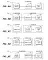
- FIGS. 6A , 6 B, 6 C, 6 D and 6 Eillustrate optional locations 602 , 604 , 606 , 608 and 610 of the clock driver and the inductor for the resonant clock distribution network of FIG. 1 .
- the clock driver 102 , the inductor 106 , and the clock netare formed on a single substrate.
- the clock driver 102is formed on a separate substrate from a single substrate on which the inductor 106 and the clock net are formed.
- the inductor 106is formed on a separate substrate from a single substrate on which the clock driver 102 and the clock net are formed.
- the inductor 106 and the clock driver 102are formed on separate substrates from a single substrate on which the clock net is formed. In the optional location 610 , the inductor 106 and the clock driver 102 are formed on a single substrate separate from a single substrate on which the clock net is formed.
- a method of distributing a clock signal in an integrated circuitincludes the steps of generating a clock signal having a selected clock frequency from a clock driver, coupling the clock signal to a clock net having a capacitive reactance, and coupling an inductor to the clock net wherein the inductor has an inductive reactance that is substantially equal and opposite to the capacitive reactance of the clock net at the selected clock frequency to minimize clock driver output current through the clock net.
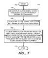
- FIG. 7illustrates a flow chart 700 for a method of distributing a clock signal according to an embodiment of the present invention.
- Step 702is the entry point of the flow chart 700 .
- a clock signalis generated having a selected clock frequency from a clock driver.
- step 706the clock signal is coupled to a clock net having a capacitive reactance.
- step 708an inductor having an inductive reactance that is substantially equal and opposite to the capacitive reactance of the clock net at the selected clock frequency is coupled to the clock net to minimize clock driver output current.
- Step 710is the exit point of the flow chart 700 .
Landscapes
- Engineering & Computer Science (AREA)
- Theoretical Computer Science (AREA)
- Physics & Mathematics (AREA)
- General Engineering & Computer Science (AREA)
- General Physics & Mathematics (AREA)
- Semiconductor Integrated Circuits (AREA)
Abstract
Description
where L is the inductance of the
Claims (16)
Priority Applications (1)
| Application Number | Priority Date | Filing Date | Title |
|---|---|---|---|
| US10/364,866US7082580B2 (en) | 2003-02-10 | 2003-02-10 | Energy recycling in clock distribution networks using on-chip inductors |
Applications Claiming Priority (1)
| Application Number | Priority Date | Filing Date | Title |
|---|---|---|---|
| US10/364,866US7082580B2 (en) | 2003-02-10 | 2003-02-10 | Energy recycling in clock distribution networks using on-chip inductors |
Publications (2)
| Publication Number | Publication Date |
|---|---|
| US20040158758A1 US20040158758A1 (en) | 2004-08-12 |
| US7082580B2true US7082580B2 (en) | 2006-07-25 |
Family
ID=32824511
Family Applications (1)
| Application Number | Title | Priority Date | Filing Date |
|---|---|---|---|
| US10/364,866Expired - Fee RelatedUS7082580B2 (en) | 2003-02-10 | 2003-02-10 | Energy recycling in clock distribution networks using on-chip inductors |
Country Status (1)
| Country | Link |
|---|---|
| US (1) | US7082580B2 (en) |
Cited By (13)
| Publication number | Priority date | Publication date | Assignee | Title |
|---|---|---|---|---|
| US20040232556A1 (en)* | 2003-05-21 | 2004-11-25 | Pitts Robert L. | Integrated circuit inductor with integrated vias |
| US20080157913A1 (en)* | 2006-12-29 | 2008-07-03 | Dongbu Hitek Co., Ltd. | Spiral inductor |
| US8704576B1 (en) | 2013-02-05 | 2014-04-22 | International Business Machines Corporation | Variable resistance switch for wide bandwidth resonant global clock distribution |
| US8742817B2 (en) | 2012-08-31 | 2014-06-03 | Advanced Micro Devices, Inc. | Controlling impedance of a switch using high impedance voltage sources to provide more efficient clocking |
| US8791726B2 (en) | 2013-01-03 | 2014-07-29 | International Business Machines Corporation | Controlled resonant power transfer |
| US8836403B2 (en) | 2012-08-31 | 2014-09-16 | Advanced Micro Devices, Inc. | Programmable clock driver |
| US8850373B2 (en) | 2013-02-22 | 2014-09-30 | International Business Machines Corporation | Setting switch size and transition pattern in a resonant clock distribution system |
| US8847652B2 (en)* | 2012-07-26 | 2014-09-30 | Taiwan Semiconductor Manufacturing Co., Ltd. | Reconfigurable and auto-reconfigurable resonant clock |
| US8854100B2 (en) | 2012-08-31 | 2014-10-07 | Advanced Micro Devices, Inc. | Clock driver for frequency-scalable systems |
| US8941432B2 (en) | 2012-08-31 | 2015-01-27 | Advanced Micro Devices, Inc. | Transitioning between resonant clocking mode and conventional clocking mode |
| US8975936B2 (en)* | 2012-08-31 | 2015-03-10 | Advanced Micro Devices, Inc. | Constraining clock skew in a resonant clocked system |
| US9054682B2 (en) | 2013-02-05 | 2015-06-09 | International Business Machines Corporation | Wide bandwidth resonant global clock distribution |
| US9058130B2 (en) | 2013-02-05 | 2015-06-16 | International Business Machines Corporation | Tunable sector buffer for wide bandwidth resonant global clock distribution |
Families Citing this family (2)
| Publication number | Priority date | Publication date | Assignee | Title |
|---|---|---|---|---|
| US6495442B1 (en)* | 2000-10-18 | 2002-12-17 | Magic Corporation | Post passivation interconnection schemes on top of the IC chips |
| US6965165B2 (en) | 1998-12-21 | 2005-11-15 | Mou-Shiung Lin | Top layers of metal for high performance IC's |
Citations (6)
| Publication number | Priority date | Publication date | Assignee | Title |
|---|---|---|---|---|
| US4866299A (en)* | 1988-08-01 | 1989-09-12 | Eastman Kodak Company | Remotely driving a CCD |
| US6437653B1 (en)* | 2000-09-28 | 2002-08-20 | Sun Microsystems, Inc. | Method and apparatus for providing a variable inductor on a semiconductor chip |
| US6448847B1 (en)* | 2000-09-12 | 2002-09-10 | Silicon Laboratories, Inc. | Apparatus and method for providing differential-to-single ended conversion and impedance transformation |
| US6473291B1 (en)* | 1999-03-16 | 2002-10-29 | Gb Aquisition Co., Inc. | Low inductance four terminal capacitor lead frame |
| US6546528B1 (en)* | 1999-04-21 | 2003-04-08 | Nec Corporation | System and method for evaluation of electric characteristics of printed-circuit boards |
| US6690243B1 (en)* | 2001-06-07 | 2004-02-10 | Cypress Semiconductor Corp. | Multi-phase voltage-controlled oscillator at modulated, operating frequency |
- 2003
- 2003-02-10USUS10/364,866patent/US7082580B2/ennot_activeExpired - Fee Related
Patent Citations (6)
| Publication number | Priority date | Publication date | Assignee | Title |
|---|---|---|---|---|
| US4866299A (en)* | 1988-08-01 | 1989-09-12 | Eastman Kodak Company | Remotely driving a CCD |
| US6473291B1 (en)* | 1999-03-16 | 2002-10-29 | Gb Aquisition Co., Inc. | Low inductance four terminal capacitor lead frame |
| US6546528B1 (en)* | 1999-04-21 | 2003-04-08 | Nec Corporation | System and method for evaluation of electric characteristics of printed-circuit boards |
| US6448847B1 (en)* | 2000-09-12 | 2002-09-10 | Silicon Laboratories, Inc. | Apparatus and method for providing differential-to-single ended conversion and impedance transformation |
| US6437653B1 (en)* | 2000-09-28 | 2002-08-20 | Sun Microsystems, Inc. | Method and apparatus for providing a variable inductor on a semiconductor chip |
| US6690243B1 (en)* | 2001-06-07 | 2004-02-10 | Cypress Semiconductor Corp. | Multi-phase voltage-controlled oscillator at modulated, operating frequency |
Non-Patent Citations (3)
| Title |
|---|
| Chi; "Salphasic Distribution of Clock Signals for Synchronous Systems"; IEEE Transactions on Computers; IEEE; vol. 43, No. 5; May 1994; pp. 597-602. |
| Huo et al.; "Silicon-Based High-Q Inductors Incorporating Electroplated Copper and Low-K BCB Dielectric"; IEEE Electron Device Letters; IEEE; vol. 23, No. 9; Sep. 2002; pp. 520-522. |
| Lihui et al.; "High Q Multilayer Spiral Inductor on Silicon Chip for 5~6 GHz"; IEEE Electron Device Letters; IEEE; vol. 23, No. 8; Aug. 2002; pp. 470-472. |
Cited By (21)
| Publication number | Priority date | Publication date | Assignee | Title |
|---|---|---|---|---|
| US20040232556A1 (en)* | 2003-05-21 | 2004-11-25 | Pitts Robert L. | Integrated circuit inductor with integrated vias |
| US7400025B2 (en)* | 2003-05-21 | 2008-07-15 | Texas Instruments Incorporated | Integrated circuit inductor with integrated vias |
| US20110133880A1 (en)* | 2003-05-21 | 2011-06-09 | Texas Instruments Incorporated | Integrated circuit inductor with integrated vias |
| US8344479B2 (en) | 2003-05-21 | 2013-01-01 | Texas Instruments Incorporated | Integrated circuit inductor with integrated vias |
| US20080157913A1 (en)* | 2006-12-29 | 2008-07-03 | Dongbu Hitek Co., Ltd. | Spiral inductor |
| US7486168B2 (en)* | 2006-12-29 | 2009-02-03 | Dongbu Hitek Co., Ltd. | Spiral inductor |
| CN101211914B (en)* | 2006-12-29 | 2010-12-08 | 东部高科股份有限公司 | Spiral sensor |
| US8847652B2 (en)* | 2012-07-26 | 2014-09-30 | Taiwan Semiconductor Manufacturing Co., Ltd. | Reconfigurable and auto-reconfigurable resonant clock |
| US8836403B2 (en) | 2012-08-31 | 2014-09-16 | Advanced Micro Devices, Inc. | Programmable clock driver |
| US8742817B2 (en) | 2012-08-31 | 2014-06-03 | Advanced Micro Devices, Inc. | Controlling impedance of a switch using high impedance voltage sources to provide more efficient clocking |
| US8854100B2 (en) | 2012-08-31 | 2014-10-07 | Advanced Micro Devices, Inc. | Clock driver for frequency-scalable systems |
| US8941432B2 (en) | 2012-08-31 | 2015-01-27 | Advanced Micro Devices, Inc. | Transitioning between resonant clocking mode and conventional clocking mode |
| US8975936B2 (en)* | 2012-08-31 | 2015-03-10 | Advanced Micro Devices, Inc. | Constraining clock skew in a resonant clocked system |
| US8791726B2 (en) | 2013-01-03 | 2014-07-29 | International Business Machines Corporation | Controlled resonant power transfer |
| US8704576B1 (en) | 2013-02-05 | 2014-04-22 | International Business Machines Corporation | Variable resistance switch for wide bandwidth resonant global clock distribution |
| US9054682B2 (en) | 2013-02-05 | 2015-06-09 | International Business Machines Corporation | Wide bandwidth resonant global clock distribution |
| US9058130B2 (en) | 2013-02-05 | 2015-06-16 | International Business Machines Corporation | Tunable sector buffer for wide bandwidth resonant global clock distribution |
| US9612612B2 (en) | 2013-02-05 | 2017-04-04 | International Business Machines Corporation | Tunable sector buffer for wide bandwidth resonant global clock distribution |
| US8850373B2 (en) | 2013-02-22 | 2014-09-30 | International Business Machines Corporation | Setting switch size and transition pattern in a resonant clock distribution system |
| US8887118B2 (en) | 2013-02-22 | 2014-11-11 | International Business Machines Corporation | Setting switch size and transition pattern in a resonant clock distribution system |
| US9268886B2 (en) | 2013-02-22 | 2016-02-23 | Globalfoundries Inc. | Setting switch size and transition pattern in a resonant clock distribution system |
Also Published As
| Publication number | Publication date |
|---|---|
| US20040158758A1 (en) | 2004-08-12 |
Similar Documents
| Publication | Publication Date | Title |
|---|---|---|
| US7082580B2 (en) | Energy recycling in clock distribution networks using on-chip inductors | |
| US6943658B2 (en) | Integrated transformer | |
| US6870456B2 (en) | Integrated transformer | |
| KR101045195B1 (en) | Inductor formed in integrated circuit | |
| Burghartz | Progress in RF inductors on silicon-understanding substrate losses | |
| US6429504B1 (en) | Multilayer spiral inductor and integrated circuits incorporating the same | |
| US7381607B2 (en) | Method of forming a spiral inductor in a semiconductor substrate | |
| US20010016409A1 (en) | High-q inductive elements | |
| TWI236763B (en) | High performance system-on-chip inductor using post passivation process | |
| EP1267391B1 (en) | A method to fabricate RF inductors with minimum area | |
| US6992871B2 (en) | Microtransformer for system-on-chip power supply | |
| US6853522B2 (en) | Microtransformer for system-on-chip power supply | |
| US7236081B2 (en) | Inductor and method of forming the same | |
| KR100929125B1 (en) | Thin Film Multi-Layer Hi-Chip Transformers Formed on Semiconductor Substrates | |
| US5918121A (en) | Method of reducing substrate losses in inductor | |
| US6420954B1 (en) | Coupled multilayer soft magnetic films for high frequency microtransformer for system-on-chip power supply | |
| Feng et al. | Super compact RFIC inductors in 0.18/spl mu/m CMOS with copper interconnects | |
| CN113451510A (en) | Semiconductor device and method of formation | |
| US6740956B1 (en) | Metal trace with reduced RF impedance resulting from the skin effect | |
| US20250105142A1 (en) | Radio frequency inductor | |
| Carchon et al. | High-Q RF inductors on standard silicon realized using wafer-level packaging techniques | |
| KR20050062069A (en) | Method of manufacturing radio frequency semiconductor device |
Legal Events
| Date | Code | Title | Description |
|---|---|---|---|
| AS | Assignment | Owner name:LSI LOGIC CORPORATION, CALIFORNIA Free format text:ASSIGNMENT OF ASSIGNORS INTEREST;ASSIGNORS:ZARKESH-HA, PAYMAN;LOH, WILLIAM;REEL/FRAME:013772/0623 Effective date:20030130 | |
| FEPP | Fee payment procedure | Free format text:PAYOR NUMBER ASSIGNED (ORIGINAL EVENT CODE: ASPN); ENTITY STATUS OF PATENT OWNER: LARGE ENTITY | |
| FPAY | Fee payment | Year of fee payment:4 | |
| FPAY | Fee payment | Year of fee payment:8 | |
| AS | Assignment | Owner name:DEUTSCHE BANK AG NEW YORK BRANCH, AS COLLATERAL AG Free format text:PATENT SECURITY AGREEMENT;ASSIGNORS:LSI CORPORATION;AGERE SYSTEMS LLC;REEL/FRAME:032856/0031 Effective date:20140506 | |
| AS | Assignment | Owner name:LSI CORPORATION, CALIFORNIA Free format text:CHANGE OF NAME;ASSIGNOR:LSI LOGIC CORPORATION;REEL/FRAME:033102/0270 Effective date:20070406 | |
| AS | Assignment | Owner name:AVAGO TECHNOLOGIES GENERAL IP (SINGAPORE) PTE. LTD Free format text:ASSIGNMENT OF ASSIGNORS INTEREST;ASSIGNOR:LSI CORPORATION;REEL/FRAME:035390/0388 Effective date:20140814 | |
| AS | Assignment | Owner name:LSI CORPORATION, CALIFORNIA Free format text:TERMINATION AND RELEASE OF SECURITY INTEREST IN PATENT RIGHTS (RELEASES RF 032856-0031);ASSIGNOR:DEUTSCHE BANK AG NEW YORK BRANCH, AS COLLATERAL AGENT;REEL/FRAME:037684/0039 Effective date:20160201 Owner name:AGERE SYSTEMS LLC, PENNSYLVANIA Free format text:TERMINATION AND RELEASE OF SECURITY INTEREST IN PATENT RIGHTS (RELEASES RF 032856-0031);ASSIGNOR:DEUTSCHE BANK AG NEW YORK BRANCH, AS COLLATERAL AGENT;REEL/FRAME:037684/0039 Effective date:20160201 | |
| AS | Assignment | Owner name:BANK OF AMERICA, N.A., AS COLLATERAL AGENT, NORTH CAROLINA Free format text:PATENT SECURITY AGREEMENT;ASSIGNOR:AVAGO TECHNOLOGIES GENERAL IP (SINGAPORE) PTE. LTD.;REEL/FRAME:037808/0001 Effective date:20160201 Owner name:BANK OF AMERICA, N.A., AS COLLATERAL AGENT, NORTH Free format text:PATENT SECURITY AGREEMENT;ASSIGNOR:AVAGO TECHNOLOGIES GENERAL IP (SINGAPORE) PTE. LTD.;REEL/FRAME:037808/0001 Effective date:20160201 | |
| AS | Assignment | Owner name:AVAGO TECHNOLOGIES GENERAL IP (SINGAPORE) PTE. LTD., SINGAPORE Free format text:TERMINATION AND RELEASE OF SECURITY INTEREST IN PATENTS;ASSIGNOR:BANK OF AMERICA, N.A., AS COLLATERAL AGENT;REEL/FRAME:041710/0001 Effective date:20170119 Owner name:AVAGO TECHNOLOGIES GENERAL IP (SINGAPORE) PTE. LTD Free format text:TERMINATION AND RELEASE OF SECURITY INTEREST IN PATENTS;ASSIGNOR:BANK OF AMERICA, N.A., AS COLLATERAL AGENT;REEL/FRAME:041710/0001 Effective date:20170119 | |
| FEPP | Fee payment procedure | Free format text:MAINTENANCE FEE REMINDER MAILED (ORIGINAL EVENT CODE: REM.) | |
| LAPS | Lapse for failure to pay maintenance fees | Free format text:PATENT EXPIRED FOR FAILURE TO PAY MAINTENANCE FEES (ORIGINAL EVENT CODE: EXP.); ENTITY STATUS OF PATENT OWNER: LARGE ENTITY | |
| STCH | Information on status: patent discontinuation | Free format text:PATENT EXPIRED DUE TO NONPAYMENT OF MAINTENANCE FEES UNDER 37 CFR 1.362 | |
| FP | Lapsed due to failure to pay maintenance fee | Effective date:20180725 |