US7080190B2 - Apparatus and method for providing transparent sharing of channel resources by multiple host machines - Google Patents
Apparatus and method for providing transparent sharing of channel resources by multiple host machinesDownload PDFInfo
- Publication number
- US7080190B2 US7080190B2US10/158,477US15847702AUS7080190B2US 7080190 B2US7080190 B2US 7080190B2US 15847702 AUS15847702 AUS 15847702AUS 7080190 B2US7080190 B2US 7080190B2
- Authority
- US
- United States
- Prior art keywords
- data
- circuit
- controller
- storage
- coupled
- Prior art date
- Legal status (The legal status is an assumption and is not a legal conclusion. Google has not performed a legal analysis and makes no representation as to the accuracy of the status listed.)
- Expired - Lifetime, expires
Links
- 238000000034methodMethods0.000titleclaimsabstractdescription18
- 238000004891communicationMethods0.000claimsabstractdescription46
- 238000013500data storageMethods0.000claimsabstractdescription44
- 239000004744fabricSubstances0.000claimsabstractdescription16
- 230000032258transportEffects0.000claimsdescription38
- 238000013519translationMethods0.000claimsdescription20
- 230000002093peripheral effectEffects0.000claimsdescription14
- 238000012546transferMethods0.000claimsdescription13
- 239000000872bufferSubstances0.000claimsdescription10
- 239000000835fiberSubstances0.000claimsdescription9
- 230000006870functionEffects0.000claimsdescription9
- 238000012545processingMethods0.000claimsdescription4
- 230000000873masking effectEffects0.000claimsdescription2
- 230000001902propagating effectEffects0.000claimsdescription2
- 230000007704transitionEffects0.000claimsdescription2
- 230000005540biological transmissionEffects0.000claims1
- 230000003139buffering effectEffects0.000description6
- 230000003287optical effectEffects0.000description3
- 238000013459approachMethods0.000description1
- 238000003491arrayMethods0.000description1
- 208000013407communication difficultyDiseases0.000description1
- 238000010276constructionMethods0.000description1
- 238000013461designMethods0.000description1
- 238000010586diagramMethods0.000description1
- 230000010354integrationEffects0.000description1
- 239000000463materialSubstances0.000description1
- 230000007246mechanismEffects0.000description1
- 230000008569processEffects0.000description1
- 230000005641tunnelingEffects0.000description1
Images


Classifications
- H—ELECTRICITY
- H04—ELECTRIC COMMUNICATION TECHNIQUE
- H04L—TRANSMISSION OF DIGITAL INFORMATION, e.g. TELEGRAPHIC COMMUNICATION
- H04L49/00—Packet switching elements
- H04L49/35—Switches specially adapted for specific applications
- H—ELECTRICITY
- H04—ELECTRIC COMMUNICATION TECHNIQUE
- H04L—TRANSMISSION OF DIGITAL INFORMATION, e.g. TELEGRAPHIC COMMUNICATION
- H04L69/00—Network arrangements, protocols or services independent of the application payload and not provided for in the other groups of this subclass
- H04L69/08—Protocols for interworking; Protocol conversion
Definitions
- the present inventiongenerally relates to the field of data storage and particularly to a system for providing transparent switched fabric data transport to a storage area network.
- Data storage networkspresent many architectural challenges and have several key requirements such as compatible data communication, and scalability. Lack of compatibility between data formats, operating systems, network protocols, storage protocols and the like, limit or preclude free transport of data across storage systems on a network. Further, in a storage network environment communicating storage system components require exclusivity to prevent miscommunication and data loss. Storage networks may also be confronted with the addition of components, such as additional storage arrays and information handling systems which may interrupt the transport of data throughout the network. Previous data storage systems fail and thus do not meet user demands.
- a monolithic data storage systema system implemented as a whole, provides a single protocol environment but is undesirable due to cost concerns and limitations in scalability. Further, a single protocol system is inherently limited by the choice of transport protocol. When implementing monolithic systems, users often discard existing components due to incompatibility. Therefore, monolithic data storage systems fail to provide scalable, heterogeneous communication protocol capable data storage.
- Scalabilityis another key concern in data storage architecture. Users of data storage systems want storage systems capable of adding components without resorting to improvised fixes. In essence, current data storage systems lack a building block ability to adapt. The scalability of a data system may also be limited due to communication protocols ill designed for particular components. Scalability may also be limited by the overall size of the data storage system itself. Consequently, data storage systems do not provide an efficient and reliable means to scale components.
- the present inventionis directed to a method, a system, an I/O module, a controller element and application specific integrated circuit (ASIC) capable of providing transparent common message passing data storage transport.
- ASICapplication specific integrated circuit
- the systemimplements I/O modules and controller elements with circuits capable of translating between communication protocols for providing transparent multi-channel data transport for mirrored data storage.
- Implementation of the system of the present inventionallows for a common data transport system and method permitting component scalability and virtualization.
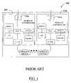
- FIG. 1is an illustration of a prior art storage system including storage controllers is shown
- FIG. 2is an illustration of an embodiment wherein a storage complex for transparent common message passing data storage transport is shown
- FIG. 3Ais an illustration of an embodiment wherein an application specific integrated circuit for utilization in switched fabric data storage transport is configured for utilization with an intelligent integrated circuit;
- FIG. 3Bis an illustration of an embodiment wherein an application specific integrated circuit for utilization in switched fabric data storage transport is configured for utilization with an unintelligent integrated circuit;
- FIG. 4Ais an illustration of an embodiment wherein a storage element for utilization in common message passing data storage transport includes controller elements with an interconnect compliant with Peripheral Component Interconnect Express (PCI Express);
- PCI ExpressPeripheral Component Interconnect Express
- FIG. 4Bis an illustration of an embodiment wherein a storage system for utilization in switched fabric data storage transport includes storage controllers with a storage controller interconnect compliant with Peripheral Component Interconnect;
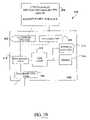
- FIG. 5is a flow diagram of a method for providing common message passing data transport.
- the storage system 100includes storage controllers 102 . Included in each storage controller is an I/O integrated circuit 104 for interfacing with host devices.
- I/O integrated circuit 104for interfacing with host devices.
- One of the drawbacks to current storage systemare that the I/O integrated circuits in utilization are limited to a particular communication protocol. In current systems, in order to access a particular logical unit number within such a storage system a host device has to utilize a protocol compatible with that particular I/O integrated circuit. Further, as multiple storage systems 100 are used together, each I/O circuit 104 only has access to storage devices contained in that single storage system 100 . The I/O circuit for one system 100 cannot access the storage devices of a separate storage system 100 .
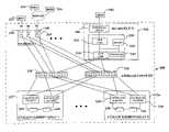
- FIG. 2an embodiment of the present invention wherein a storage complex system 200 for common message passing data transport is shown.
- the present inventionallows for transparent mapped data transport over an internal switched fabric link, thus providing scalability and common message passing while providing apparent exclusivity for controllers.
- I/O modulesIncluded in the system 200 are I/O modules.
- I/O modules 1 204 through “N” 206are shown.
- the storage complex of the present inventionis scalable with respect to storage complex components.
- the present inventionfurther allows for scalability with respect to host devices and or host device networks.
- I/O modules included in the storage complex system 200may be coupled either directly or via a network to a host device or a plurality of host devices depending on the implementation.
- Host devices 202include servers, information handling systems and the like.
- a host interface I/O circuitis included in the I/O module.
- I/O circuitsare suitable for data transport with a host device or multiple host devices utilizing a common protocol over the physical connection. Suitable protocols include SCSI Remote DMA Protocol (SRP) over InfiniBand (IB), Small Computer System Interface over TCP/IP (iSCSI) over Ethernet, Fibre Channel Protocol (FCP) over Fibre Channel (FC), and the like.
- SRPSCSI Remote DMA Protocol
- IBInfiniBand
- iSCSISmall Computer System Interface over TCP/IP
- FCPFibre Channel Protocol
- FCFibre Channel
- I/O circuit 208implements FCP over FC for communication with a host device 202 .
- an I/O circuit 238 utilizing SRP over IBcommunicates with a host device 232 .
- an I/O circuit 240communicates via a FC Fabric with host devices 234 and 236 utilizing FCP over FC. It is to be apparent that various protocols and physical connections may be implemented without departing from the scope and spirit of the present invention.
- Data transfers in target mode to these I/O circuits (chips)typically use a vendor unique message passing scheme that consists of a microprocessor pre-posting command buffers to the I/O chip on initialization. Command buffers specify an area in microprocessor memory where an incoming storage command from a host device are deposited by the I/O chip.
- the I/O chip vendor unique message passing schemealso has a mechanism to allow the one and only one microprocessor to specify a data transfer message indicating to the I/O chip where in memory to get/put the data (scatter gather list), as well as the direction of the data flow.
- the message passing schemeallows the one and only one microprocessor the ability to specify a completion message after the data transfer is complete that indicates that the entire I/O command has completed. It is the function of the I/O chip to convert from this I/O chip specific message passing scheme to a physical interface such as Fibre Channel, and a standard I/O storage protocol such as FCP. It is also noted that there are I/O chips which are unintelligent in which a microprocessor must discretely implement the I/O protocol by way of a specific driver.
- An application specific integrated circuit (ASIC) 210is included in the I/O module “N” 206 .
- the ASIC 210functions to translate generally between the vendor unique message passing protocol implemented by the I/O Chip and the common message passing protocol implemented internally in the storage complex 200 .
- ASICs of the present inventionare capable of providing masking and funneling to interface I/O circuits.
- the ASIC of the present inventionis suitable for emulating data transfers for the associated I/O circuit. Translation and routing may be based on host world wide name, a unique host identifier, logical unit number and the like.
- the ASICis capable of virtualization of data storage such as striping, and logical unit number concatenation as well as virtualization of hosts, ports, LUNS and volumes. Striping includes interleaving data to multiple controller elements and concatenation includes filling a portion of data on one controller element and then moving to another controller element, such that multiple separate volumes on multiple controller elements appear to a host as a single logical unit.
- At least one link coreis included in the I/O module ASIC 210 .
- Link coresare suitable for communication in compliance with InfiniBand (IB), Gigabit Ethernet (GE), Fibre Channel (FC), PCI Express, Peripheral Component Interconnect (PCI), Peripheral Component Interconnect-X (PCI-X) and the like.
- I/O module ASIC 206includes a first link core 212 suitable for utilization in compliance with PCI Express to communicate with the I/O circuit 208 and host 202 associated with I/O module N 206 and a second link core 214 compliant at least minimally with InfiniBand, when the storage complex utilizes InfiniBand. It will be apparent that transactions occurring over link cores of the storage complex 200 may be compliant with other protocols or some level of compliance as contemplated by one of ordinary skill in the art without departing from the spirit and scope of the present invention.
- a processor 218is coupled to the first and second link cores 212 and 214 .
- an ARM (Advanced RISC Machine) core type processor 218is implemented.
- other processorsare implemented.
- the processor 218is suitable for translating messages between the first and second link cores 212 and 214 , wherein translation is based on at least one of host world wide name, a unique host identifier and logical unit number.
- a memory 216 coupled to the processor 218is suitable for processor code storage and execution, buffering data transports as well as storing commands such as from preposted command buffers, or command pool routing function providing a routing table.
- Bufferingmay include buffering data as well as read write commands and the like.
- Routing tablesmay include host world wide name, logical unit number (LUN), unique host identifiers, controller element identifiers for directing data transports though the storage complex 200 .
- LUNlogical unit number
- controller element identifiersfor directing data transports though the storage complex 200 .
- pre-post command buffersto each I/O module ASIC which is discovered.
- I/O module ASICfor I/O modules 1 though “N”
- Each controller element processorindependently discover each I/O module ASIC in the storage complex system.
- Routing tables that are contained in each ASICare then configured to determine which controller element host commands are routed to.
- commandsmay reside either in part or in whole on the processor such as firmware as well and it is the intention to encompass and include such changes as contemplated by one of ordinary skill in the art.
- components included in the ASICmay be implemented as independent external components such as to allow for upgrades and the like.
- Two switches 220are included in the system 200 .
- the switches 220are coupled to at least one link core 214 of the I/O ASIC 210 .
- the switches 220are suitable for communication at least minimally in compliance with InfiniBand communication protocol.
- the second link core 214 of the I/O module ASIC 210coupled to each of the switches, is InfiniBand compliant and may allow tunneling PCI or PCI Express through InfiniBand for increased transparency. In further embodiments other communication protocols are implemented as contemplated by one of ordinary skill in the art.
- Each switchis capable of propagating data including providing mirrored data to storage elements and controlling communication.
- Storage elementsare individually coupled to each switch 220 .
- Storage element one 222 through N 224are shown. It is to be understood that the present invention is scalable with respect to storage elements.
- Controller elementsare included in each of the storage elements. Referring to storage element “N” 224 , two controller elements 226 and 228 are included. Each storage element in the storage complex system 200 may or may not be substantially similar to storage element “N” 224 . Including at least two controller elements allows for write cache enablement.
- each storage elementincludes a plurality of storage devices 230 .
- Storage devicesinclude hard drives, tape drives, optical storage devices, magnetic-optical devices, and the like.
- Optical storage devicesmay include CD-ROM, CD-R, DVD and the like.
- Various combinations/arrangements of devices including various RAID configurationsmay be desirable and it is within the spirit and scope of the present invention to include these combinations and arrangements.
- storage element 222may contain storage devices suited for high I/O operations while storage element 224 may contain storage devices designed for high bandwidth.
- pre-mapped transfersmay target specific storage elements/storage devices customized for desired capabilities.
- storage devicesmay be external to the storage element, such as to facilitate upgrades and the like.
- FIG. 3Aan embodiment of an I/O module ASIC 300 suitably configured for interfacing with an intelligent I/O circuit 308 is shown.
- the I/O circuit 308is substantially the same as the I/O circuit 208 described with respect to FIG. 2 .
- the ASIC 300 of the present embodimentinteracts via a message passing interface via I/O circuit 308 .
- the ASIC 300 of the present inventionallows for translation and common message passing through a storage complex such as generally described with respect to FIG. 1 .
- the ASIC 300permits apparent exclusivity and transparent data transport between storage complex components, such as controller and an intelligent I/O integrated circuit 308 with internal processor minimized interrupts.
- Link coresmay implement, a variety of standards such as InfiniBand (IB), Gigabit Ethernet (GE), Fibre Channel (FC), PCI Express, Peripheral Component Interconnect (PCI), Peripheral Component Interconnect-X (PCI-X) and the like.
- IBInfiniBand
- GEGigabit Ethernet
- FCFibre Channel
- PCI ExpressPeripheral Component Interconnect
- PCI-XPeripheral Component Interconnect-X
- the module ASIC 300 of the present embodimentutilizes a PCI Express compliant link core 302 coupled to the I/O integrated circuit 308 .
- a transaction logic 318is coupled to the PCI Express link core 302 and an InfiniBand link core 306 suitable for integration into an InfiniBand based storage complex providing switched fabric link substantially as described in regards to FIG. 2 .
- Utilization of the transaction logic 318allows for translation between link cores, for example, PCI Express 302 , PCI-X 304 , and InfiniBand 306 .
- translation logic 318may be implemented by state machines which translate bus cycles and DMA operations from one link core to the other, and can be controlled or monitored by ARM core processor 310 .
- ARM core processor 310various processors capable of controlling the transition logic 318 and capable of interfacing with a memory 314 are contemplated.
- Routing function 312may be included either as software, firmware, hardware or a combination thereof for implementation with the ARM core 310 processor.
- the memory 314may be capable of storing routing function software tables until requested by the ARM core 310 .
- the memory 314may maintain pre-mapped targets for read/write commands, routing table data such as host world wide name, a unique host identifier, LUN, controller identification and the like.
- the memory 314may be additionally suitable for buffering data. For example, if ASIC 300 receives data from more then one controller data may be buffered to avoid miscommunication.
- the I/O module ASIC of FIG. 3Ais shown suitably configured for interfacing with an unintelligent I/O integrated circuit 318 .
- the ASIC of the present embodimentis substantially similar to the ASIC described with respect to FIGS. 2 and 3A .
- the unintelligent I/O integrated circuit 318is coupled to the PCI-X link core 304 included in the ASIC 300 .
- the present configurationadditionally allows for use of the ASIC 300 with an unintelligent register based interface integrated circuit 318 , such as Agilent Tachyon integrated circuit and the like.
- the ASIC 300is capable of executing an appropriate software driver for implementing a specific storage protocol and translating between the unintelligent registers of integrated circuit 318 , and the internal message passing interface of the complex. Translation and routing may be maintained based on host world wide name, a unique host identifier, logical unit number and the like. In additional embodiments the ASIC is suitable for virtualization such as striping and logical unit number concatenation as well as virtualization of ports and volumes, as discussed above.
- FIG. 4Aan embodiment of a storage element including at least two controller elements per storage element 400 are shown.
- Two controllers 402 and 404are shown.
- the first controller 402 and the second controller 404are substantially similar.
- various combinations and arrangements of controller elementsmay be utilized as contemplated by one of ordinary skill in the art without departing from the scope and spirit of the present invention.
- the controller elementincludes an ASIC 406 .
- the controller 404may implement ASICs as are described generally with regard to the I/O module ASICs in regards to FIGS. 2 , 3 A and 3 B respectively 210 and 300 . In application in which ASIC is implemented into a controller element to function in direct memory access mode the ASIC processor may not be included.
- a controller element interconnect 408is coupled to the controller ASIC 406 .
- the storage controller interconnect 408is suitable for interacting with a storage I/O circuit 418 coupled to a plurality of storage devices 402 .
- the interconnectis compliant with PCI Express.
- an interconnect 324is compliant with PCI and the like as contemplated by one of ordinary skill in the art.
- a controller element central processing unit (CPU) 410is coupled to the interconnect 408 .
- the controller CPU 410is suitable for controlling operation of the interconnect 408 .
- the controller CPU 410may be capable of providing RAID engine control over the plurality of storage devices 420 configured for RAID operation via the interconnect 408 and I/O circuit.
- a memory 412is coupled to the controller CPU 410 and the interconnect 408 .
- the memoryis suitable for storing software capable of encoding instruction for operation of the storage controller CPU 410 for example, preposted buffer commands and the like.
- controller element 402may be at least one memory controller 414 and an associated memory 430 .
- the memory controller 414 and the memory 430are suitable for utilization in buffering data transfers and the like.
- a RAID specific memory controllermay be implemented.
- the storage elementincludes at least two controller elements 426 substantially similar to the storage element 400 as discussed with respect to FIG. 4A and to the ASICs 210 and 300 discussed with respect to FIGS. 2 and 3 , respectively.
- the storage system 422includes a controller element interconnect 424 compliant with PCI.
- the controller ASIC 428is configured for interface with the PCI based interconnect 424 .
- the controller interconnect 424 and the ASIC 428are compliant with other protocols as contemplated by one of ordinary skill in the art without departing from the scope and spirit of the present invention.
- the controller element 426includes a memory controller 432 such as a XOR memory controller coupled to the interconnect 424 .
- a memory 430is associated with the XOR controller.
- the XOR memory controller and the associated memory 430are suitable of storing data, such as stored data for transport, from the PCI interconnect 424 .
- An I/O module associated with an I/O interface ASICis connected to one or multiple host devices, either direct or via a storage area network. Initially, on power up, the controller elements discover the I/O module ASICs, and set up routing tables and pre-posted command buffers to the ASIC. The ASIC in turn, preposts command buffers to the I/O circuit. During normal operation, commands are received from the host device 502 via a I/O circuit, commands include read/write command.
- the I/O circuitUpon receiving host commands the I/O circuit direct memory accesses to the preposted buffer and interrupts the module processor 504 . For example, with regard to FIG. 2 , the host 202 sends a read command via I/O circuit 208 to the ASIC processor 218 and associated memory 216 .
- a processor implementing the present methodinterprets the command 506 .
- Interpretingincludes translating into a common message passing interface where translation is based on at least one of host world wide name, unique host identifier, and LUN.
- the processorutilizing routing data determines the controller element pointed to by the host/LUN combination for the desired data and the like.
- the ASICmay implement the routing function by way of a linear search engine such as discussed generally with respect to FIGS. 3A and 3B for translation.
- the ASIC processorthen writes the command to the appropriate controller elements pre-posted buffer area 508 .
- the controller elementis then interrupted and processes the command.
- the controller elementthen sends a data transfer message to the I/O module ASIC by way of the common protocol 510 .
- the controller element processorobtains the data from the particular storage device.
- a write command datais transferred to the controller element for the particular storage device for buffering/writing.
- a processorsuch as the I/O module processor 218 , FIG. 2 implementing the steps of the present method then posts a send data operation to the I/O interface circuit, such as I/O circuit 208 described in FIG. 2 .
- the ASICthen transfers data from/to the host by way of directly coupled DMA 512 to/from the controller element data transfer memory, such as described generally in FIG. 4B .
- the I/O circuitsubsequently sends either an auto reply to the host, or a reply specified by the controller element.
- an I/O circuit implementing the current methodinterrupts the I/O Module ASIC processor, and provides an operation complete status message 514 , which is then sent back to the appropriate controller element by way of a completion message.
- a controller central processorsuch as the central processing unit discussed in regards to FIGS. 4A and 4B implementing the present method issues a status message such as indicating complete transfer 514 .
- the methods disclosedmay be implemented as sets of instructions or software readable by a device. Further, it is understood that the specific order or hierarchy of steps in the methods disclosed are examples of exemplary approaches. Based upon design preferences, it is understood that the specific order or hierarchy of steps in the method can be rearranged while remaining within the scope of the present invention.
- the accompanying method claimspresent elements of the various steps in a sample order, and are not meant to be limited to the specific order or hierarchy presented.
- One of the embodiments of the inventioncan be implemented as sets of instructions resident in the memory of one or more information handling systems, which may include memory for storing a program of instructions and a processor for performing the program of instruction, wherein the program of instructions configures the processor and information handling system.
- the set of instructionsmay be stored in another readable memory device, for example in a hard disk drive or in a removable medium such as an optical disc.
Landscapes
- Engineering & Computer Science (AREA)
- Computer Networks & Wireless Communication (AREA)
- Signal Processing (AREA)
- Computer Security & Cryptography (AREA)
- Bus Control (AREA)
Abstract
Description
Claims (32)
Priority Applications (2)
| Application Number | Priority Date | Filing Date | Title |
|---|---|---|---|
| US10/158,477US7080190B2 (en) | 2002-05-30 | 2002-05-30 | Apparatus and method for providing transparent sharing of channel resources by multiple host machines |
| US10/198,684US7493404B2 (en) | 2002-05-30 | 2002-07-18 | Apparatus and method for providing transparent sharing of channel resources by multiple host machines utilizing mixed mode block and file protocols |
Applications Claiming Priority (1)
| Application Number | Priority Date | Filing Date | Title |
|---|---|---|---|
| US10/158,477US7080190B2 (en) | 2002-05-30 | 2002-05-30 | Apparatus and method for providing transparent sharing of channel resources by multiple host machines |
Related Child Applications (1)
| Application Number | Title | Priority Date | Filing Date |
|---|---|---|---|
| US10/198,684Continuation-In-PartUS7493404B2 (en) | 2002-05-30 | 2002-07-18 | Apparatus and method for providing transparent sharing of channel resources by multiple host machines utilizing mixed mode block and file protocols |
Publications (2)
| Publication Number | Publication Date |
|---|---|
| US20030225724A1 US20030225724A1 (en) | 2003-12-04 |
| US7080190B2true US7080190B2 (en) | 2006-07-18 |
Family
ID=29582696
Family Applications (1)
| Application Number | Title | Priority Date | Filing Date |
|---|---|---|---|
| US10/158,477Expired - LifetimeUS7080190B2 (en) | 2002-05-30 | 2002-05-30 | Apparatus and method for providing transparent sharing of channel resources by multiple host machines |
Country Status (1)
| Country | Link |
|---|---|
| US (1) | US7080190B2 (en) |
Cited By (19)
| Publication number | Priority date | Publication date | Assignee | Title |
|---|---|---|---|---|
| US20040098518A1 (en)* | 2002-11-20 | 2004-05-20 | Beckett Richard C. | Integrated circuit having multiple modes of operation |
| US20040168041A1 (en)* | 2003-02-25 | 2004-08-26 | Internet Machines Corp. | Flexible interface device |
| US20050015515A1 (en)* | 2003-05-23 | 2005-01-20 | Heppenstall Mark F. | Method and apparatus for transferring data across a protocol bridge |
| US20060013222A1 (en)* | 2002-06-28 | 2006-01-19 | Brocade Communications Systems, Inc. | Apparatus and method for internet protocol data processing in a storage processing device |
| US20060092928A1 (en)* | 2004-10-15 | 2006-05-04 | Dell Products L.P. | System and method for providing a shareable input/output device in a PCI express environment |
| US20060168367A1 (en)* | 2002-11-20 | 2006-07-27 | Beckett Richard C | Integrated circuit having multiple modes of operation |
| US7152136B1 (en)* | 2004-08-03 | 2006-12-19 | Altera Corporation | Implementation of PCI express |
| US7257655B1 (en)* | 2004-10-13 | 2007-08-14 | Altera Corporation | Embedded PCI-Express implementation |
| US20080244055A1 (en)* | 2007-03-30 | 2008-10-02 | Hitachi, Ltd. | Computer that manages devices |
| US20080304504A1 (en)* | 2003-11-18 | 2008-12-11 | Heath Stewart | PCI Express Switch with Backwards Compatibility |
| US20090150609A1 (en)* | 2003-05-22 | 2009-06-11 | Katsuyoshi Suzuki | Disk array apparatus and method for controlling the same |
| US20100257301A1 (en)* | 2009-04-07 | 2010-10-07 | Lsi Corporation | Configurable storage array controller |
| US20110167220A1 (en)* | 2003-02-17 | 2011-07-07 | Hitachi, Ltd. | Storage system for holding a remaining available lifetime of a logical storage region |
| US8468300B2 (en) | 2003-11-28 | 2013-06-18 | Hitachi, Ltd. | Storage system having plural controllers and an expansion housing with drive units |
| US10698613B1 (en) | 2019-04-19 | 2020-06-30 | EMC IP Holding Company LLC | Host processing of I/O operations |
| US10698844B1 (en) | 2019-04-19 | 2020-06-30 | EMC IP Holding Company LLC | Intelligent external storage system interface |
| US10740259B1 (en) | 2019-04-19 | 2020-08-11 | EMC IP Holding Company LLC | Host mapping logical storage devices to physical storage devices |
| US11151063B2 (en)* | 2019-04-19 | 2021-10-19 | EMC IP Holding Company LLC | Host system directly connected to internal switching fabric of storage system |
| US11500549B2 (en) | 2019-04-19 | 2022-11-15 | EMC IP Holding Company LLC | Secure host access to storage system resources via storage system interface and internal switching fabric |
Families Citing this family (7)
| Publication number | Priority date | Publication date | Assignee | Title |
|---|---|---|---|---|
| US20040006587A1 (en)* | 2002-07-02 | 2004-01-08 | Dell Products L.P. | Information handling system and method for clustering with internal cross coupled storage |
| US7454552B2 (en)* | 2003-11-18 | 2008-11-18 | Topside Research, Llc | Switch with transparent and non-transparent ports |
| US7694047B1 (en)* | 2005-02-17 | 2010-04-06 | Qlogic, Corporation | Method and system for sharing input/output devices |
| US9384160B2 (en)* | 2008-09-04 | 2016-07-05 | Avago Technologies General Ip (Singapore) Pte. Ltd. | Methods and controllers for affiliation managment |
| US9112790B2 (en)* | 2013-06-25 | 2015-08-18 | Google Inc. | Fabric network |
| JP6074056B2 (en) | 2013-11-07 | 2017-02-01 | 株式会社日立製作所 | Computer system and data control method |
| CN108959134B (en)* | 2017-05-24 | 2022-02-15 | 微软技术许可有限责任公司 | Communication for field programmable gate array devices |
Citations (10)
| Publication number | Priority date | Publication date | Assignee | Title |
|---|---|---|---|---|
| US5915102A (en)* | 1996-11-06 | 1999-06-22 | International Business Machines Corporation | Common arbiter interface device with arbitration configuration for centralized common bus arbitration |
| US6275874B1 (en)* | 1998-12-23 | 2001-08-14 | Nortel Networks Limited | System for producing communication codes responsive to communication signals, translating communication codes into peripheral codes, and producing signals for communicating with peripheral responsive to peripheral codes |
| US6311222B1 (en)* | 1998-10-07 | 2001-10-30 | Nortel Networks Corporation | Translator memory management system |
| US20020194304A1 (en)* | 2001-06-15 | 2002-12-19 | Spencer Cramer | System and method for providing virtual online engineering of a production environment |
| US6640278B1 (en)* | 1999-03-25 | 2003-10-28 | Dell Products L.P. | Method for configuration and management of storage resources in a storage network |
| US6708232B2 (en)* | 2000-06-29 | 2004-03-16 | Hitachi, Ltd. | Data migration method, protocol converter and switching apparatus using it |
| US6724747B1 (en)* | 1997-12-03 | 2004-04-20 | Telcordia Technologies, Inc., A Corp. Of Delaware | Method and system for media connectivity over a packet-based network |
| US6763402B2 (en)* | 2000-05-25 | 2004-07-13 | Bnl Technologies, Inc. | Data storage subsystem |
| US6779083B2 (en)* | 2001-07-13 | 2004-08-17 | Hitachi, Ltd. | Security for logical unit in storage subsystem |
| US6789152B2 (en)* | 1997-12-31 | 2004-09-07 | Crossroads Systems, Inc. | Storage router and method for providing virtual local storage |
- 2002
- 2002-05-30USUS10/158,477patent/US7080190B2/ennot_activeExpired - Lifetime
Patent Citations (10)
| Publication number | Priority date | Publication date | Assignee | Title |
|---|---|---|---|---|
| US5915102A (en)* | 1996-11-06 | 1999-06-22 | International Business Machines Corporation | Common arbiter interface device with arbitration configuration for centralized common bus arbitration |
| US6724747B1 (en)* | 1997-12-03 | 2004-04-20 | Telcordia Technologies, Inc., A Corp. Of Delaware | Method and system for media connectivity over a packet-based network |
| US6789152B2 (en)* | 1997-12-31 | 2004-09-07 | Crossroads Systems, Inc. | Storage router and method for providing virtual local storage |
| US6311222B1 (en)* | 1998-10-07 | 2001-10-30 | Nortel Networks Corporation | Translator memory management system |
| US6275874B1 (en)* | 1998-12-23 | 2001-08-14 | Nortel Networks Limited | System for producing communication codes responsive to communication signals, translating communication codes into peripheral codes, and producing signals for communicating with peripheral responsive to peripheral codes |
| US6640278B1 (en)* | 1999-03-25 | 2003-10-28 | Dell Products L.P. | Method for configuration and management of storage resources in a storage network |
| US6763402B2 (en)* | 2000-05-25 | 2004-07-13 | Bnl Technologies, Inc. | Data storage subsystem |
| US6708232B2 (en)* | 2000-06-29 | 2004-03-16 | Hitachi, Ltd. | Data migration method, protocol converter and switching apparatus using it |
| US20020194304A1 (en)* | 2001-06-15 | 2002-12-19 | Spencer Cramer | System and method for providing virtual online engineering of a production environment |
| US6779083B2 (en)* | 2001-07-13 | 2004-08-17 | Hitachi, Ltd. | Security for logical unit in storage subsystem |
Cited By (33)
| Publication number | Priority date | Publication date | Assignee | Title |
|---|---|---|---|---|
| US20060013222A1 (en)* | 2002-06-28 | 2006-01-19 | Brocade Communications Systems, Inc. | Apparatus and method for internet protocol data processing in a storage processing device |
| US20060168367A1 (en)* | 2002-11-20 | 2006-07-27 | Beckett Richard C | Integrated circuit having multiple modes of operation |
| US7640481B2 (en)* | 2002-11-20 | 2009-12-29 | Intel Corporation | Integrated circuit having multiple modes of operation |
| US7543085B2 (en) | 2002-11-20 | 2009-06-02 | Intel Corporation | Integrated circuit having multiple modes of operation |
| US20040098518A1 (en)* | 2002-11-20 | 2004-05-20 | Beckett Richard C. | Integrated circuit having multiple modes of operation |
| US20110167220A1 (en)* | 2003-02-17 | 2011-07-07 | Hitachi, Ltd. | Storage system for holding a remaining available lifetime of a logical storage region |
| US8370572B2 (en) | 2003-02-17 | 2013-02-05 | Hitachi, Ltd. | Storage system for holding a remaining available lifetime of a logical storage region |
| US8190858B2 (en) | 2003-02-25 | 2012-05-29 | Topside Research, Llc | Interface device for interfacing a main processor to processing engines and classifier engines, and methods for configuring and operating interface devices |
| US20040168041A1 (en)* | 2003-02-25 | 2004-08-26 | Internet Machines Corp. | Flexible interface device |
| US8200898B2 (en) | 2003-05-22 | 2012-06-12 | Hitachi, Ltd. | Storage apparatus and method for controlling the same |
| US8429342B2 (en) | 2003-05-22 | 2013-04-23 | Hitachi, Ltd. | Drive apparatus and method for controlling the same |
| US8151046B2 (en) | 2003-05-22 | 2012-04-03 | Hitachi, Ltd. | Disk array apparatus and method for controlling the same |
| US20090150609A1 (en)* | 2003-05-22 | 2009-06-11 | Katsuyoshi Suzuki | Disk array apparatus and method for controlling the same |
| US20110022796A1 (en)* | 2003-05-22 | 2011-01-27 | Hitachi, Ltd. | Disk array apparatus and method for controllng the same |
| US7225274B2 (en)* | 2003-05-23 | 2007-05-29 | Applied Micro Circuits Corporation | Method and apparatus for transferring data across a protocol bridge |
| US20050015515A1 (en)* | 2003-05-23 | 2005-01-20 | Heppenstall Mark F. | Method and apparatus for transferring data across a protocol bridge |
| US20080304504A1 (en)* | 2003-11-18 | 2008-12-11 | Heath Stewart | PCI Express Switch with Backwards Compatibility |
| US20110016258A1 (en)* | 2003-11-18 | 2011-01-20 | Heath Stewart | Routing Data Units Between Different Address Domains |
| US7814259B2 (en) | 2003-11-18 | 2010-10-12 | Internet Machines, Llc | PCI express switch with backwards compatibility |
| US7945722B2 (en) | 2003-11-18 | 2011-05-17 | Internet Machines, Llc | Routing data units between different address domains |
| US8468300B2 (en) | 2003-11-28 | 2013-06-18 | Hitachi, Ltd. | Storage system having plural controllers and an expansion housing with drive units |
| US7152136B1 (en)* | 2004-08-03 | 2006-12-19 | Altera Corporation | Implementation of PCI express |
| US7257655B1 (en)* | 2004-10-13 | 2007-08-14 | Altera Corporation | Embedded PCI-Express implementation |
| US20060092928A1 (en)* | 2004-10-15 | 2006-05-04 | Dell Products L.P. | System and method for providing a shareable input/output device in a PCI express environment |
| US7827269B2 (en)* | 2007-03-30 | 2010-11-02 | Hitachi, Ltd. | System and method for managing networked storage devices with a plurality of logical units |
| US20080244055A1 (en)* | 2007-03-30 | 2008-10-02 | Hitachi, Ltd. | Computer that manages devices |
| US7913027B2 (en)* | 2009-04-07 | 2011-03-22 | Lsi Corporation | Configurable storage array controller |
| US20100257301A1 (en)* | 2009-04-07 | 2010-10-07 | Lsi Corporation | Configurable storage array controller |
| US10698613B1 (en) | 2019-04-19 | 2020-06-30 | EMC IP Holding Company LLC | Host processing of I/O operations |
| US10698844B1 (en) | 2019-04-19 | 2020-06-30 | EMC IP Holding Company LLC | Intelligent external storage system interface |
| US10740259B1 (en) | 2019-04-19 | 2020-08-11 | EMC IP Holding Company LLC | Host mapping logical storage devices to physical storage devices |
| US11151063B2 (en)* | 2019-04-19 | 2021-10-19 | EMC IP Holding Company LLC | Host system directly connected to internal switching fabric of storage system |
| US11500549B2 (en) | 2019-04-19 | 2022-11-15 | EMC IP Holding Company LLC | Secure host access to storage system resources via storage system interface and internal switching fabric |
Also Published As
| Publication number | Publication date |
|---|---|
| US20030225724A1 (en) | 2003-12-04 |
Similar Documents
| Publication | Publication Date | Title |
|---|---|---|
| US7080190B2 (en) | Apparatus and method for providing transparent sharing of channel resources by multiple host machines | |
| US7167929B2 (en) | Integrated-circuit implementation of a storage-shelf router and a path controller card for combined use in high-availability mass-storage-device shelves that may be incorporated within disk arrays, and a storage-shelf-interface tunneling method and system | |
| US7353321B2 (en) | Integrated-circuit implementation of a storage-shelf router and a path controller card for combined use in high-availability mass-storage-device shelves that may be incorporated within disk arrays | |
| US7743178B2 (en) | Method and apparatus for SATA tunneling over fibre channel | |
| US7917682B2 (en) | Multi-protocol controller that supports PCIe, SAS and enhanced Ethernet | |
| KR101340176B1 (en) | Smart Scalable Storage Switch Architecture | |
| US7457902B2 (en) | Lock and release mechanism for out-of-order frame prevention and support of native command queueing in FC-SATA | |
| US8321650B2 (en) | Alignment-unit-based virtual formatting methods and devices employing the methods | |
| US7801120B2 (en) | Method and system for efficient queue management | |
| US8281084B2 (en) | Method and interface for access to memory within a first electronic device by a second electronic device | |
| JP4871880B2 (en) | Storage shelf router integrated circuit | |
| EP1807753B1 (en) | Method and system for transferring data directly between storage devices in a storage area network | |
| US20160021031A1 (en) | Global shared memory switch | |
| US7493404B2 (en) | Apparatus and method for providing transparent sharing of channel resources by multiple host machines utilizing mixed mode block and file protocols | |
| US7421520B2 (en) | High-speed I/O controller having separate control and data paths | |
| US20060064531A1 (en) | Method and system for optimizing data transfer in networks |
Legal Events
| Date | Code | Title | Description |
|---|---|---|---|
| AS | Assignment | Owner name:LSI LOGIC CORPORATION, CALIFORNIA Free format text:ASSIGNMENT OF ASSIGNORS INTEREST;ASSIGNOR:WEBER, BRET S.;REEL/FRAME:012955/0500 Effective date:20020530 | |
| STCF | Information on status: patent grant | Free format text:PATENTED CASE | |
| FEPP | Fee payment procedure | Free format text:PAYOR NUMBER ASSIGNED (ORIGINAL EVENT CODE: ASPN); ENTITY STATUS OF PATENT OWNER: LARGE ENTITY | |
| FPAY | Fee payment | Year of fee payment:4 | |
| AS | Assignment | Owner name:NETAPP, INC., CALIFORNIA Free format text:ASSIGNMENT OF ASSIGNORS INTEREST;ASSIGNOR:LSI LOGIC CORPORATION;REEL/FRAME:026661/0205 Effective date:20110506 | |
| FPAY | Fee payment | Year of fee payment:8 | |
| AS | Assignment | Owner name:NETAPP, INC., CALIFORNIA Free format text:ASSIGNMENT OF ASSIGNORS INTEREST;ASSIGNOR:LSI LOGIC CORPORATION;REEL/FRAME:036552/0557 Effective date:20110506 | |
| MAFP | Maintenance fee payment | Free format text:PAYMENT OF MAINTENANCE FEE, 12TH YEAR, LARGE ENTITY (ORIGINAL EVENT CODE: M1553) Year of fee payment:12 |