US7078770B2 - Fully depleted silicon-on-insulator CMOS logic - Google Patents
Fully depleted silicon-on-insulator CMOS logicDownload PDFInfo
- Publication number
- US7078770B2 US7078770B2US10/950,726US95072604AUS7078770B2US 7078770 B2US7078770 B2US 7078770B2US 95072604 AUS95072604 AUS 95072604AUS 7078770 B2US7078770 B2US 7078770B2
- Authority
- US
- United States
- Prior art keywords
- region
- silicon
- insulator
- drain
- coupled
- Prior art date
- Legal status (The legal status is an assumption and is not a legal conclusion. Google has not performed a legal analysis and makes no representation as to the accuracy of the status listed.)
- Expired - Lifetime, expires
Links
Images


Classifications
- H—ELECTRICITY
- H10—SEMICONDUCTOR DEVICES; ELECTRIC SOLID-STATE DEVICES NOT OTHERWISE PROVIDED FOR
- H10D—INORGANIC ELECTRIC SEMICONDUCTOR DEVICES
- H10D30/00—Field-effect transistors [FET]
- H10D30/60—Insulated-gate field-effect transistors [IGFET]
- H10D30/69—IGFETs having charge trapping gate insulators, e.g. MNOS transistors
- H10D30/693—Vertical IGFETs having charge trapping gate insulators
- G—PHYSICS
- G11—INFORMATION STORAGE
- G11C—STATIC STORES
- G11C16/00—Erasable programmable read-only memories
- G11C16/02—Erasable programmable read-only memories electrically programmable
- G11C16/04—Erasable programmable read-only memories electrically programmable using variable threshold transistors, e.g. FAMOS
- G11C16/0466—Erasable programmable read-only memories electrically programmable using variable threshold transistors, e.g. FAMOS comprising cells with charge storage in an insulating layer, e.g. metal-nitride-oxide-silicon [MNOS], silicon-oxide-nitride-oxide-silicon [SONOS]
- G11C16/0475—Erasable programmable read-only memories electrically programmable using variable threshold transistors, e.g. FAMOS comprising cells with charge storage in an insulating layer, e.g. metal-nitride-oxide-silicon [MNOS], silicon-oxide-nitride-oxide-silicon [SONOS] comprising two or more independent storage sites which store independent data
- H—ELECTRICITY
- H10—SEMICONDUCTOR DEVICES; ELECTRIC SOLID-STATE DEVICES NOT OTHERWISE PROVIDED FOR
- H10B—ELECTRONIC MEMORY DEVICES
- H10B43/00—EEPROM devices comprising charge-trapping gate insulators
- H10B43/30—EEPROM devices comprising charge-trapping gate insulators characterised by the memory core region
- H—ELECTRICITY
- H10—SEMICONDUCTOR DEVICES; ELECTRIC SOLID-STATE DEVICES NOT OTHERWISE PROVIDED FOR
- H10B—ELECTRONIC MEMORY DEVICES
- H10B69/00—Erasable-and-programmable ROM [EPROM] devices not provided for in groups H10B41/00 - H10B63/00, e.g. ultraviolet erasable-and-programmable ROM [UVEPROM] devices
- H—ELECTRICITY
- H10—SEMICONDUCTOR DEVICES; ELECTRIC SOLID-STATE DEVICES NOT OTHERWISE PROVIDED FOR
- H10D—INORGANIC ELECTRIC SEMICONDUCTOR DEVICES
- H10D30/00—Field-effect transistors [FET]
- H10D30/01—Manufacture or treatment
- H10D30/021—Manufacture or treatment of FETs having insulated gates [IGFET]
- H10D30/0413—Manufacture or treatment of FETs having insulated gates [IGFET] of FETs having charge-trapping gate insulators, e.g. MNOS transistors
- H—ELECTRICITY
- H10—SEMICONDUCTOR DEVICES; ELECTRIC SOLID-STATE DEVICES NOT OTHERWISE PROVIDED FOR
- H10D—INORGANIC ELECTRIC SEMICONDUCTOR DEVICES
- H10D30/00—Field-effect transistors [FET]
- H10D30/60—Insulated-gate field-effect transistors [IGFET]
- H10D30/67—Thin-film transistors [TFT]
- H10D30/6704—Thin-film transistors [TFT] having supplementary regions or layers in the thin films or in the insulated bulk substrates for controlling properties of the device
- H10D30/6708—Thin-film transistors [TFT] having supplementary regions or layers in the thin films or in the insulated bulk substrates for controlling properties of the device for preventing the kink effect or the snapback effect, e.g. discharging the minority carriers of the channel region for preventing bipolar effect
- H10D30/6711—Thin-film transistors [TFT] having supplementary regions or layers in the thin films or in the insulated bulk substrates for controlling properties of the device for preventing the kink effect or the snapback effect, e.g. discharging the minority carriers of the channel region for preventing bipolar effect by using electrodes contacting the supplementary regions or layers
- H—ELECTRICITY
- H10—SEMICONDUCTOR DEVICES; ELECTRIC SOLID-STATE DEVICES NOT OTHERWISE PROVIDED FOR
- H10D—INORGANIC ELECTRIC SEMICONDUCTOR DEVICES
- H10D30/00—Field-effect transistors [FET]
- H10D30/60—Insulated-gate field-effect transistors [IGFET]
- H10D30/69—IGFETs having charge trapping gate insulators, e.g. MNOS transistors
- H10D30/691—IGFETs having charge trapping gate insulators, e.g. MNOS transistors having more than two programming levels
- H—ELECTRICITY
- H10—SEMICONDUCTOR DEVICES; ELECTRIC SOLID-STATE DEVICES NOT OTHERWISE PROVIDED FOR
- H10D—INORGANIC ELECTRIC SEMICONDUCTOR DEVICES
- H10D30/00—Field-effect transistors [FET]
- H10D30/60—Insulated-gate field-effect transistors [IGFET]
- H10D30/791—Arrangements for exerting mechanical stress on the crystal lattice of the channel regions
- H10D30/797—Arrangements for exerting mechanical stress on the crystal lattice of the channel regions being in source or drain regions, e.g. SiGe source or drain
- H—ELECTRICITY
- H10—SEMICONDUCTOR DEVICES; ELECTRIC SOLID-STATE DEVICES NOT OTHERWISE PROVIDED FOR
- H10D—INORGANIC ELECTRIC SEMICONDUCTOR DEVICES
- H10D64/00—Electrodes of devices having potential barriers
- H10D64/01—Manufacture or treatment
- H10D64/031—Manufacture or treatment of data-storage electrodes
- H10D64/037—Manufacture or treatment of data-storage electrodes comprising charge-trapping insulators
- H—ELECTRICITY
- H10—SEMICONDUCTOR DEVICES; ELECTRIC SOLID-STATE DEVICES NOT OTHERWISE PROVIDED FOR
- H10D—INORGANIC ELECTRIC SEMICONDUCTOR DEVICES
- H10D86/00—Integrated devices formed in or on insulating or conducting substrates, e.g. formed in silicon-on-insulator [SOI] substrates or on stainless steel or glass substrates
- H10D86/01—Manufacture or treatment
- H—ELECTRICITY
- H10—SEMICONDUCTOR DEVICES; ELECTRIC SOLID-STATE DEVICES NOT OTHERWISE PROVIDED FOR
- H10D—INORGANIC ELECTRIC SEMICONDUCTOR DEVICES
- H10D86/00—Integrated devices formed in or on insulating or conducting substrates, e.g. formed in silicon-on-insulator [SOI] substrates or on stainless steel or glass substrates
- H10D86/201—Integrated devices formed in or on insulating or conducting substrates, e.g. formed in silicon-on-insulator [SOI] substrates or on stainless steel or glass substrates the substrates comprising an insulating layer on a semiconductor body, e.g. SOI
- G—PHYSICS
- G11—INFORMATION STORAGE
- G11C—STATIC STORES
- G11C2211/00—Indexing scheme relating to digital stores characterized by the use of particular electric or magnetic storage elements; Storage elements therefor
- G11C2211/401—Indexing scheme relating to cells needing refreshing or charge regeneration, i.e. dynamic cells
- G11C2211/4016—Memory devices with silicon-on-insulator cells
Definitions
- the present inventionrelates generally to silicon-on-insulator devices and in particular the present invention relates to fully depleted silicon-on-insulator logic.
- SOIsilicon-on-insulator
- CMOScomplementary metal-oxide-semiconductor
- FIG. 1illustrates a typical SOI semiconductor.
- the transistoris formed in the silicon layer 101 that is over the insulator 102 .
- the insulatoris formed on top of the substrate 103 .
- the drain/source regions 105 and 106are formed within the silicon layer 101 .
- the gate 107is formed above the partially depleted channel 109 .
- a floating body 110is within the depleted region 112 and results from the partial depletion.
- the silicon film used for SOI transistorsmust be perfect crystalline silicon.
- the insulator layeris not crystalline. It is very difficult to make perfect crystalline silicon-on-oxide or silicon with other insulators since the insulator layer's crystalline properties are so different from the pure silicon. If perfect crystalline silicon is not obtained, defects will find their way onto the SOI film. This degrades the transistor performance.
- SOSfully depleted silicon-on-sapphire
- the present inventionencompasses a method for generating a fully depleted body structure in a silicon-on-insulator device.
- the methodprovides an extractor contact coupled to the body structure.
- An extractor voltageis provided such that the extractor contact is reverse biased and minority carriers in the body structure are removed.
- FIG. 1shows a cross sectional view of a typical silicon-on-insulator transistor.
- FIG. 2shows a top view of one embodiment of a silicon-on-insulator transistor of the present invention.
- FIG. 3shows a cross sectional view of a fully depleted silicon-on-insulator inverter using one embodiment of the reverse biased extractor contact method of the present invention.
- FIG. 4shows a cross sectional view of an NROM flash memory cell using one embodiment of the method of the present invention to fully deplete silicon-on-insulator transistors.
- FIG. 5shows a top view of the NROM flash memory cell of FIG. 4 .
- FIG. 6shows a cross sectional view of a typical prior art partially depleted NROM flash memory cell.
- FIG. 7shows a cross sectional view of a fully depleted NROM flash memory cell using one embodiment of the extractor contact reverse bias method of the present invention.
- FIG. 8shows a cross sectional view of a fully depleted vertical NROM flash memory cell using one embodiment of the extractor contact reverse bias method of the present invention.
- FIG. 9shows an electronic system in accordance with a fully depleted silicon-on-insulator transistor of the present invention.
- FIG. 2illustrates a top view of one embodiment of a silicon-on-insulator (SOI) NMOS transistor of the present invention.
- SOIsilicon-on-insulator
- the present inventionuses reverse biasing of the body contacts, also known as extractors, to provide a fully depleted transistor.
- the extractorsremove minority carriers from the body region of a partially depleted MOS device. This eliminates the effect where the drain current does not stay constant as the drain voltage increases when a device is operating in the saturation mode.
- the SOI transistor illustrated in FIG. 2is comprised of two drain/source regions 201 and 202 .
- these regionsare n+ wells formed in the silicon layer.
- the width of these regions 201 and 202is indicated as W. In one embodiment, the width is one micron or less. Alternate embodiments use other widths. In another embodiment, transistors wider than one micron can be realized through parallel transistors.
- a p+ region extractor contact 205is formed in the silicon layer substantially adjacent the two drain/source regions 201 and 202 .
- the extractor contact 205would be implemented on an n+ silicon region.
- a gate 207is formed above and between the drain/source regions 201 and 202 .
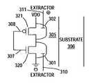
- FIG. 3illustrates a cross sectional view of one embodiment of an SOI inverter using the reverse biased extractors of the present invention.
- the inverteris comprised of two transistors, an NMOS device 320 and a PMOS device 321 .
- Each transistor 320 and 321has an associated extractor contact 310 and 311 .
- Each extractor 310 and 311is coupled to the body structure 301 and 302 of each transistor.
- the NMOS body structure 301is comprised of a p-type silicon while the PMOS body structure 302 is comprised of an n-type silicon.
- Each transistor 320 and 321has an associated control gate 307 and 308 respectively.
- the control gate 307is located above the drain/source regions (not shown).
- the insulator 305 and substrate 306are also illustrated.
- the extractors 310 and 311are reverse biased with respect to the substrate potential.
- a voltage that is greater than the drain voltage, V DDis applied.
- the NMOS transistor's extractor 301is reverse biased by applying a voltage that is less than ground potential.
- the additional voltages needed to bias the extractor nodes above V DD and below groundcan be generated by charge pump circuits that are well known in the art. These pumps are not illustrated.
- the extractor reverse biasing of the present inventionchanges the partially depleted SOI structure to fully depleted without a floating body region. Charge that is generated by leakage currents, impact ionization, or ionizing radiation is extracted and not collected on a floating body or near the source. Removal of any excess charge generated by leakage currents or impact ionization will be by diffusion current and not be drift along a highly resistive p-type body region.
- Flash memories based on electron trappingare well known and commonly used electronic components. Smaller cell sizes have always been one of the more important issues for low bit cost and high density flash memory. Conventional planar NOR flash memory cells require a large number of contacts. NAND flash memories are a series of devices with contacts at the end of a long series of bits. This results in a very high bit density.
- NROM flash memory devicesemploy charge trapping in a silicon nitride layer. NROM devices can be implemented with the CMOS process.
- FIG. 4illustrates a cross sectional view of an NROM flash memory cell using one embodiment of the method of the present invention to fully deplete silicon-on-insulator transistors.
- the NROM flash memory cell of FIG. 4is a NOR array cell with virtual ground bit lines.
- the NROM flash memory cellis comprised of the SOI layer 410 on the insulator 411 .
- the bit lines 401 and 402are n-type regions in this embodiment. When the extractor contacts (shown in FIG. 5 ) are reverse biased, the body region 403 between the bit lines is fully depleted.
- the oxide-nitride-oxide (ONO) region 405is between the control gate 406 and the silicon layer 410 .
- FIG. 5illustrates a top view of the NROM flash memory cell of FIG. 4 .
- This viewshows the bit lines 401 and 402 and the control gate 406 .
- the extractor contacts 501 and 502are p-type regions over the depleted body 403 .
- One problem with typical partially depleted NROM flash memory cellsis that the floating body causes a problem during an erase operation.
- a negative erase potentialis applied to the control gate in an NROM device, the partially depleted body terminates many of the electric field lines as illustrated in the cross sectional view of FIG. 6 .
- the body potentialfloats negative causing the electric field 601 that is attempting to erase the charge 603 , stored in the ONO composite gate insulator 605 , to become smaller and the erase speed slower.
- the extractor reverse biasing method of the present inventioncan be applied to an NROM flash memory cell to increase erase speed. Additionally, the erase speed will not drift and change with time due to floating body effects as occurs in partially depleted devices.
- FIG. 7illustrates a cross sectional view of an NROM flash memory cell that uses one embodiment of the method of the present invention for fully depleting silicon-on-insulator transistors.
- the charge 703 stored in the ONO layer 705is erased by the electric field 701 without a drift in the erase speed.
- the fully depleted body 710does not have a negative effect on the electric field 701 as in a partially depleted device.
- FIGS. 4–7illustrate NROM flash memory cells
- alternate embodimentsmay use conventional flash memory cells on SOI. If there is a floating body, the negative control gate potential couples through the floating gate to the floating body. The floating body then changes to a negative potential. This decreases the electric field used for negative control gate to source erase, thus slowing the erase operation.
- the fully depleted SOI transistor bodies of the present inventioneliminate this effect.
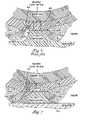
- FIG. 8illustrates a vertical NROM 301 that can use the reverse biased extractors of the present invention to produce a fully depleted body structure.
- the vertical NROM 801includes a vertical metal oxide semiconductor field effect transistor (MOSFET) 801 extending outwardly from a substrate 800 .
- the MOSFET 801has a first source/drain region 802 that, in this n-channel embodiment, includes a heavily doped (n+) n-type region layered with an n-type doped region.
- the MOSFET 801includes a similarly structured second source/drain region 806 .
- a channel region 805is located in the vertical pillar between the first and the second source/drain regions, 802 and 806 respectively. As shown in the embodiment of FIG. 8 , a gate 809 is separated from the channel region 805 by a gate insulator 807 as is located alongside of the vertical pillar opposing the channel region 805 .
- the gate insulator 807includes a gate insulator formed of an oxide-nitride-oxide (ONO) composition 807 .
- the gate insulator 807includes a gate insulator selected from the group of silicon dioxide (SiO 2 ) formed by wet oxidation, silicon oxynitride (SON), silicon rich oxide (SRO), and silicon rich aluminum oxide (Al 2 O 3 ).
- the gate insulator 807has a thickness of approximately 10 nanometers (nm).
- the gate insulator 807includes a gate insulator 807 selected from the group of silicon rich aluminum oxide insulators, silicon rich oxides with inclusions of nanoparticles of silicon, silicon oxide insulators with inclusions of nanoparticles of silicon carbide, and silicon oxycarbide insulators.
- the gate insulator 807includes a composite layer selected from the group of an oxide-aluminum oxide (Al 2 O 3 )-oxide composite layer, an oxide-silicon oxycarbide-oxide composite layer, and an oxide-nitride-aluminum oxide composite layer.
- the aluminum oxide top layerhas a higher dielectric constant so that this layer can be thicker in order to preclude tunneling to and from the control gate to the nitride storage layer.
- Alternate embodimentsuse other high dielectric constant insulators as the top layer.
- the gate insulator 807includes a gate insulator 807 that includes a composite layer, or a non-stoichiometric single layer of two or more materials selected from the group of silicon (Si), titanium (Ti), and tantalum (Ta).
- FIG. 9illustrates a functional block diagram of a memory device 900 coupled to a processor 910 and incorporating one embodiment of an SOI memory cell of the present invention.
- the processor 910may be a microprocessor, a processor, or some other type of controlling circuitry.
- the memory device 900 and the processor 910form part of an electronic system 920 .
- the memory deviceincludes an array of SOI-structured memory cells 930 as described in the various embodiments above.
- the memory cellsare non-volatile floating-gate memory cells and the memory array 930 is arranged in banks of rows and columns.
- An address buffer circuit 940is provided to latch address signals provided on address input connections A 0 –Ax 942 . Address signals are received and decoded by a row decoder 944 and a column decoder 946 to access the memory array 930 . It will be appreciated by those skilled in the art, with the benefit of the present description, that the number of address input connections depends on the density and architecture of the memory array 930 . That is, the number of addresses increases with both increased memory cell counts and increased bank and block counts.
- the memory device 900reads data in the memory array 930 by sensing voltage or current changes in the memory array columns using sense/latch circuitry 950 .
- the sense/latch circuitryin one embodiment, is coupled to read and latch a row of data from the memory array 930 .
- Data input and output buffer circuitry 960is included for bi-directional data communication over a plurality of data connections 962 with the controller 910 .
- Write circuitry 955is provided to write data to the memory array.
- Control circuitry 970decodes signals provided on control connections 972 from the processor 910 . These signals are used to control the operations on the memory array 930 , including data read, data write, and erase operations.
- the control circuitry 970may be a state machine, a sequencer, or some other type of controller.
- the flash memory device illustrated in FIG. 9has been simplified to facilitate a basic understanding of the features of the memory. A more detailed understanding of internal circuitry and functions of flash memories are known to those skilled in the art.
- CMOS logic and SRAM memoriesIn static CMOS logic and SRAM memories, the floating bodies cause threshold voltages and switching speeds to be variable and complex functions of the switching history of a particular logic gate. In dynamic logic DRAM memories, the floating bodies cause excess charge leakage and short retention times that can result in data loss. Conventional flash memories and NROM memories experience reduced erase fields and slower erase times due to floating bodies.
Landscapes
- Engineering & Computer Science (AREA)
- Microelectronics & Electronic Packaging (AREA)
- Semiconductor Memories (AREA)
- Thin Film Transistor (AREA)
- Non-Volatile Memory (AREA)
- Metal-Oxide And Bipolar Metal-Oxide Semiconductor Integrated Circuits (AREA)
Abstract
Description
Claims (20)
Priority Applications (3)
| Application Number | Priority Date | Filing Date | Title |
|---|---|---|---|
| US10/950,726US7078770B2 (en) | 2003-10-09 | 2004-09-27 | Fully depleted silicon-on-insulator CMOS logic |
| US11/391,087US7973370B2 (en) | 2003-10-09 | 2006-03-28 | Fully depleted silicon-on-insulator CMOS logic |
| US13/099,459US8174081B2 (en) | 2003-10-09 | 2011-05-03 | Fully depleted silicon-on-insulator CMOS logic |
Applications Claiming Priority (2)
| Application Number | Priority Date | Filing Date | Title |
|---|---|---|---|
| US10/682,590US6830963B1 (en) | 2003-10-09 | 2003-10-09 | Fully depleted silicon-on-insulator CMOS logic |
| US10/950,726US7078770B2 (en) | 2003-10-09 | 2004-09-27 | Fully depleted silicon-on-insulator CMOS logic |
Related Parent Applications (1)
| Application Number | Title | Priority Date | Filing Date |
|---|---|---|---|
| US10/682,590DivisionUS6830963B1 (en) | 2003-10-09 | 2003-10-09 | Fully depleted silicon-on-insulator CMOS logic |
Related Child Applications (1)
| Application Number | Title | Priority Date | Filing Date |
|---|---|---|---|
| US11/391,087ContinuationUS7973370B2 (en) | 2003-10-09 | 2006-03-28 | Fully depleted silicon-on-insulator CMOS logic |
Publications (2)
| Publication Number | Publication Date |
|---|---|
| US20050077564A1 US20050077564A1 (en) | 2005-04-14 |
| US7078770B2true US7078770B2 (en) | 2006-07-18 |
Family
ID=33490985
Family Applications (4)
| Application Number | Title | Priority Date | Filing Date |
|---|---|---|---|
| US10/682,590Expired - LifetimeUS6830963B1 (en) | 2003-10-09 | 2003-10-09 | Fully depleted silicon-on-insulator CMOS logic |
| US10/950,726Expired - LifetimeUS7078770B2 (en) | 2003-10-09 | 2004-09-27 | Fully depleted silicon-on-insulator CMOS logic |
| US11/391,087Expired - LifetimeUS7973370B2 (en) | 2003-10-09 | 2006-03-28 | Fully depleted silicon-on-insulator CMOS logic |
| US13/099,459Expired - Fee RelatedUS8174081B2 (en) | 2003-10-09 | 2011-05-03 | Fully depleted silicon-on-insulator CMOS logic |
Family Applications Before (1)
| Application Number | Title | Priority Date | Filing Date |
|---|---|---|---|
| US10/682,590Expired - LifetimeUS6830963B1 (en) | 2003-10-09 | 2003-10-09 | Fully depleted silicon-on-insulator CMOS logic |
Family Applications After (2)
| Application Number | Title | Priority Date | Filing Date |
|---|---|---|---|
| US11/391,087Expired - LifetimeUS7973370B2 (en) | 2003-10-09 | 2006-03-28 | Fully depleted silicon-on-insulator CMOS logic |
| US13/099,459Expired - Fee RelatedUS8174081B2 (en) | 2003-10-09 | 2011-05-03 | Fully depleted silicon-on-insulator CMOS logic |
Country Status (7)
| Country | Link |
|---|---|
| US (4) | US6830963B1 (en) |
| EP (1) | EP1673813B1 (en) |
| JP (1) | JP4792397B2 (en) |
| KR (1) | KR100761628B1 (en) |
| CN (1) | CN1868068B (en) |
| SG (1) | SG130200A1 (en) |
| WO (1) | WO2005038932A2 (en) |
Cited By (3)
| Publication number | Priority date | Publication date | Assignee | Title |
|---|---|---|---|---|
| US20060170050A1 (en)* | 2003-10-09 | 2006-08-03 | Micron Technology, Inc. | Fully depleted silicon-on-insulator CMOS logic |
| CN102291103A (en)* | 2011-07-05 | 2011-12-21 | 浙江大学 | Dynamic body biasing class-C inverter and application thereof |
| CN102394594A (en)* | 2011-08-31 | 2012-03-28 | 浙江大学 | Numerical control body bias type C inverter |
Families Citing this family (42)
| Publication number | Priority date | Publication date | Assignee | Title |
|---|---|---|---|---|
| US6804502B2 (en) | 2001-10-10 | 2004-10-12 | Peregrine Semiconductor Corporation | Switch circuit and method of switching radio frequency signals |
| US7719343B2 (en) | 2003-09-08 | 2010-05-18 | Peregrine Semiconductor Corporation | Low noise charge pump method and apparatus |
| US7202523B2 (en)* | 2003-11-17 | 2007-04-10 | Micron Technology, Inc. | NROM flash memory devices on ultrathin silicon |
| US7256450B2 (en)* | 2004-03-24 | 2007-08-14 | Micron Technology, Inc. | NROM memory device with a high-permittivity gate dielectric formed by the low temperature oxidation of metals |
| US7102191B2 (en) | 2004-03-24 | 2006-09-05 | Micron Technologies, Inc. | Memory device with high dielectric constant gate dielectrics and metal floating gates |
| EP3570374B1 (en) | 2004-06-23 | 2022-04-20 | pSemi Corporation | Integrated rf front end |
| US7212440B2 (en)* | 2004-12-30 | 2007-05-01 | Sandisk Corporation | On-chip data grouping and alignment |
| JP4284300B2 (en)* | 2005-05-02 | 2009-06-24 | 株式会社東芝 | Semiconductor memory device |
| US7890891B2 (en) | 2005-07-11 | 2011-02-15 | Peregrine Semiconductor Corporation | Method and apparatus improving gate oxide reliability by controlling accumulated charge |
| US9653601B2 (en) | 2005-07-11 | 2017-05-16 | Peregrine Semiconductor Corporation | Method and apparatus for use in improving linearity of MOSFETs using an accumulated charge sink-harmonic wrinkle reduction |
| US20080076371A1 (en) | 2005-07-11 | 2008-03-27 | Alexander Dribinsky | Circuit and method for controlling charge injection in radio frequency switches |
| US7910993B2 (en) | 2005-07-11 | 2011-03-22 | Peregrine Semiconductor Corporation | Method and apparatus for use in improving linearity of MOSFET's using an accumulated charge sink |
| USRE48965E1 (en) | 2005-07-11 | 2022-03-08 | Psemi Corporation | Method and apparatus improving gate oxide reliability by controlling accumulated charge |
| US8742502B2 (en) | 2005-07-11 | 2014-06-03 | Peregrine Semiconductor Corporation | Method and apparatus for use in improving linearity of MOSFETs using an accumulated charge sink-harmonic wrinkle reduction |
| US7829938B2 (en)* | 2005-07-14 | 2010-11-09 | Micron Technology, Inc. | High density NAND non-volatile memory device |
| US7482619B2 (en)* | 2005-09-07 | 2009-01-27 | Samsung Electronics Co., Ltd. | Charge trap memory device comprising composite of nanoparticles and method of fabricating the charge trap memory device |
| US7612371B2 (en)* | 2006-01-17 | 2009-11-03 | International Business Machines Corporation | Structure to monitor arcing in the processing steps of metal layer build on silicon-on-insulator semiconductors |
| KR101277402B1 (en) | 2007-01-26 | 2013-06-20 | 마이크론 테크놀로지, 인코포레이티드 | Floating-body dram transistor comprising source/drain regions separated from the gated body region |
| US7960772B2 (en)* | 2007-04-26 | 2011-06-14 | Peregrine Semiconductor Corporation | Tuning capacitance to enhance FET stack voltage withstand |
| US8320191B2 (en) | 2007-08-30 | 2012-11-27 | Infineon Technologies Ag | Memory cell arrangement, method for controlling a memory cell, memory array and electronic device |
| US7648868B2 (en)* | 2007-10-31 | 2010-01-19 | International Business Machines Corporation | Metal-gated MOSFET devices having scaled gate stack thickness |
| US9024700B2 (en) | 2008-02-28 | 2015-05-05 | Peregrine Semiconductor Corporation | Method and apparatus for use in digitally tuning a capacitor in an integrated circuit device |
| US9030248B2 (en)* | 2008-07-18 | 2015-05-12 | Peregrine Semiconductor Corporation | Level shifter with output spike reduction |
| US9660590B2 (en) | 2008-07-18 | 2017-05-23 | Peregrine Semiconductor Corporation | Low-noise high efficiency bias generation circuits and method |
| EP2421132A2 (en) | 2008-07-18 | 2012-02-22 | Peregrine Semiconductor Corporation | Charge pump with a plurality of transfer control switches |
| US8278651B2 (en)* | 2008-12-22 | 2012-10-02 | E I Du Pont De Nemours And Company | Electronic device including 1,7-phenanthroline derivative |
| US8723260B1 (en) | 2009-03-12 | 2014-05-13 | Rf Micro Devices, Inc. | Semiconductor radio frequency switch with body contact |
| WO2012054642A1 (en)* | 2010-10-20 | 2012-04-26 | Peregrine Semiconductor Corporation | Method and apparatus for use in improving linearity of mosfets using an accumulated charge sink - harmonic wrinkle reduction |
| TWI596769B (en)* | 2011-01-13 | 2017-08-21 | 半導體能源研究所股份有限公司 | Semiconductor device and semiconductor storage device |
| US9264053B2 (en) | 2011-01-18 | 2016-02-16 | Peregrine Semiconductor Corporation | Variable frequency charge pump |
| US8443306B1 (en)* | 2012-04-03 | 2013-05-14 | Taiwan Semiconductor Manufacturing Co., Ltd. | Planar compatible FDSOI design architecture |
| US9590674B2 (en) | 2012-12-14 | 2017-03-07 | Peregrine Semiconductor Corporation | Semiconductor devices with switchable ground-body connection |
| US20150236748A1 (en) | 2013-03-14 | 2015-08-20 | Peregrine Semiconductor Corporation | Devices and Methods for Duplexer Loss Reduction |
| US9406695B2 (en) | 2013-11-20 | 2016-08-02 | Peregrine Semiconductor Corporation | Circuit and method for improving ESD tolerance and switching speed |
| US9831857B2 (en) | 2015-03-11 | 2017-11-28 | Peregrine Semiconductor Corporation | Power splitter with programmable output phase shift |
| US9948281B2 (en) | 2016-09-02 | 2018-04-17 | Peregrine Semiconductor Corporation | Positive logic digitally tunable capacitor |
| US20190172920A1 (en)* | 2017-12-06 | 2019-06-06 | Nanya Technology Corporation | Junctionless transistor device and method for preparing the same |
| US10236872B1 (en) | 2018-03-28 | 2019-03-19 | Psemi Corporation | AC coupling modules for bias ladders |
| US10886911B2 (en) | 2018-03-28 | 2021-01-05 | Psemi Corporation | Stacked FET switch bias ladders |
| US10505530B2 (en) | 2018-03-28 | 2019-12-10 | Psemi Corporation | Positive logic switch with selectable DC blocking circuit |
| US11476849B2 (en) | 2020-01-06 | 2022-10-18 | Psemi Corporation | High power positive logic switch |
| US11810951B2 (en) | 2021-12-16 | 2023-11-07 | Globalfoundries U.S. Inc. | Semiconductor-on-insulator field effect transistor with performance-enhancing source/drain shapes and/or materials |
Citations (96)
| Publication number | Priority date | Publication date | Assignee | Title |
|---|---|---|---|---|
| US4184207A (en) | 1978-01-27 | 1980-01-15 | Texas Instruments Incorporated | High density floating gate electrically programmable ROM |
| US4420504A (en) | 1980-12-22 | 1983-12-13 | Raytheon Company | Programmable read only memory |
| US4755864A (en) | 1984-12-25 | 1988-07-05 | Kabushiki Kaisha Toshiba | Semiconductor read only memory device with selectively present mask layer |
| US4881114A (en) | 1986-05-16 | 1989-11-14 | Actel Corporation | Selectively formable vertical diode circuit element |
| US5241496A (en) | 1991-08-19 | 1993-08-31 | Micron Technology, Inc. | Array of read-only memory cells, eacch of which has a one-time, voltage-programmable antifuse element constructed within a trench shared by a pair of cells |
| US5330930A (en) | 1992-12-31 | 1994-07-19 | Chartered Semiconductor Manufacturing Pte Ltd. | Formation of vertical polysilicon resistor having a nitride sidewall for small static RAM cell |
| US5378647A (en) | 1993-10-25 | 1995-01-03 | United Microelectronics Corporation | Method of making a bottom gate mask ROM device |
| US5379253A (en) | 1992-06-01 | 1995-01-03 | National Semiconductor Corporation | High density EEPROM cell array with novel programming scheme and method of manufacture |
| US5397725A (en) | 1993-10-28 | 1995-03-14 | National Semiconductor Corporation | Method of controlling oxide thinning in an EPROM or flash memory array |
| US5467305A (en) | 1992-03-12 | 1995-11-14 | International Business Machines Corporation | Three-dimensional direct-write EEPROM arrays and fabrication methods |
| US5576236A (en) | 1995-06-28 | 1996-11-19 | United Microelectronics Corporation | Process for coding and code marking read-only memory |
| US5768192A (en) | 1996-07-23 | 1998-06-16 | Saifun Semiconductors, Ltd. | Non-volatile semiconductor memory cell utilizing asymmetrical charge trapping |
| US5792697A (en) | 1997-01-07 | 1998-08-11 | United Microelectronics Corporation | Method for fabricating a multi-stage ROM |
| US5858841A (en) | 1997-01-20 | 1999-01-12 | United Microelectronics Corporation | ROM device having memory units arranged in three dimensions, and a method of making the same |
| US5911106A (en) | 1996-08-29 | 1999-06-08 | Nec Corporation | Semiconductor memory device and fabrication thereof |
| US5942781A (en)* | 1998-06-08 | 1999-08-24 | Sun Microsystems, Inc. | Tunable threshold SOI device using back gate well |
| US5946558A (en) | 1997-02-05 | 1999-08-31 | United Microelectronics Corp. | Method of making ROM components |
| US5966603A (en) | 1997-06-11 | 1999-10-12 | Saifun Semiconductors Ltd. | NROM fabrication method with a periphery portion |
| US5994745A (en) | 1994-04-08 | 1999-11-30 | United Microelectronics Corp. | ROM device having shaped gate electrodes and corresponding code implants |
| US6011725A (en) | 1997-08-01 | 2000-01-04 | Saifun Semiconductors, Ltd. | Two bit non-volatile electrically erasable and programmable semiconductor memory cell utilizing asymmetrical charge trapping |
| US6028342A (en) | 1996-11-22 | 2000-02-22 | United Microelectronics Corp. | ROM diode and a method of making the same |
| US6030871A (en) | 1998-05-05 | 2000-02-29 | Saifun Semiconductors Ltd. | Process for producing two bit ROM cell utilizing angled implant |
| US6044022A (en) | 1999-02-26 | 2000-03-28 | Tower Semiconductor Ltd. | Programmable configuration for EEPROMS including 2-bit non-volatile memory cell arrays |
| US6078090A (en)* | 1997-04-02 | 2000-06-20 | Siliconix Incorporated | Trench-gated Schottky diode with integral clamping diode |
| US6081456A (en) | 1999-02-04 | 2000-06-27 | Tower Semiconductor Ltd. | Bit line control circuit for a memory array using 2-bit non-volatile memory cells |
| US6108240A (en) | 1999-02-04 | 2000-08-22 | Tower Semiconductor Ltd. | Implementation of EEPROM using intermediate gate voltage to avoid disturb conditions |
| US6134156A (en) | 1999-02-04 | 2000-10-17 | Saifun Semiconductors Ltd. | Method for initiating a retrieval procedure in virtual ground arrays |
| US6133102A (en) | 1998-06-19 | 2000-10-17 | Wu; Shye-Lin | Method of fabricating double poly-gate high density multi-state flat mask ROM cells |
| US6147904A (en) | 1999-02-04 | 2000-11-14 | Tower Semiconductor Ltd. | Redundancy method and structure for 2-bit non-volatile memory cells |
| US6157570A (en) | 1999-02-04 | 2000-12-05 | Tower Semiconductor Ltd. | Program/erase endurance of EEPROM memory cells |
| US6172396B1 (en) | 1998-02-03 | 2001-01-09 | Worldwide Semiconductor Manufacturing Corp. | ROM structure and method of manufacture |
| US6174758B1 (en) | 1999-03-03 | 2001-01-16 | Tower Semiconductor Ltd. | Semiconductor chip having fieldless array with salicide gates and methods for making same |
| US6175523B1 (en) | 1999-10-25 | 2001-01-16 | Advanced Micro Devices, Inc | Precharging mechanism and method for NAND-based flash memory devices |
| US6181597B1 (en) | 1999-02-04 | 2001-01-30 | Tower Semiconductor Ltd. | EEPROM array using 2-bit non-volatile memory cells with serial read operations |
| US6184089B1 (en) | 1999-01-27 | 2001-02-06 | United Microelectronics Corp. | Method of fabricating one-time programmable read only memory |
| US6201737B1 (en) | 2000-01-28 | 2001-03-13 | Advanced Micro Devices, Inc. | Apparatus and method to characterize the threshold distribution in an NROM virtual ground array |
| US6204529B1 (en) | 1999-08-27 | 2001-03-20 | Hsing Lan Lung | 8 bit per cell non-volatile semiconductor memory structure utilizing trench technology and dielectric floating gate |
| US6208557B1 (en) | 1999-05-21 | 2001-03-27 | National Semiconductor Corporation | EPROM and flash memory cells with source-side injection and a gate dielectric that traps hot electrons during programming |
| US6207504B1 (en) | 1998-07-29 | 2001-03-27 | United Semiconductor Corp. | Method of fabricating flash erasable programmable read only memory |
| US6215702B1 (en) | 2000-02-16 | 2001-04-10 | Advanced Micro Devices, Inc. | Method of maintaining constant erasing speeds for non-volatile memory cells |
| US6218695B1 (en) | 1999-06-28 | 2001-04-17 | Tower Semiconductor Ltd. | Area efficient column select circuitry for 2-bit non-volatile memory cells |
| US6222768B1 (en) | 2000-01-28 | 2001-04-24 | Advanced Micro Devices, Inc. | Auto adjusting window placement scheme for an NROM virtual ground array |
| US20010001075A1 (en) | 1997-03-25 | 2001-05-10 | Vantis Corporation | Process for fabricating semiconductor memory device with high data retention including silicon nitride etch stop layer formed at high temperature with low hydrogen ion concentration |
| US6240020B1 (en) | 1999-10-25 | 2001-05-29 | Advanced Micro Devices | Method of bitline shielding in conjunction with a precharging scheme for nand-based flash memory devices |
| US6243300B1 (en) | 2000-02-16 | 2001-06-05 | Advanced Micro Devices, Inc. | Substrate hole injection for neutralizing spillover charge generated during programming of a non-volatile memory cell |
| US6249027B1 (en) | 1998-06-08 | 2001-06-19 | Sun Microsystems, Inc. | Partially depleted SOI device having a dedicated single body bias means |
| US20010004332A1 (en) | 1998-05-20 | 2001-06-21 | Saifun Semiconductors Ltd. | NROM cell with improved programming, erasing and cycling |
| US6251731B1 (en) | 1998-08-10 | 2001-06-26 | Acer Semiconductor Manufacturing, Inc. | Method for fabricating high-density and high-speed nand-type mask roms |
| US6255166B1 (en) | 1999-08-05 | 2001-07-03 | Aalo Lsi Design & Device Technology, Inc. | Nonvolatile memory cell, method of programming the same and nonvolatile memory array |
| US6256231B1 (en) | 1999-02-04 | 2001-07-03 | Tower Semiconductor Ltd. | EEPROM array using 2-bit non-volatile memory cells and method of implementing same |
| US6266281B1 (en) | 2000-02-16 | 2001-07-24 | Advanced Micro Devices, Inc. | Method of erasing non-volatile memory cells |
| US6269023B1 (en) | 2000-05-19 | 2001-07-31 | Advanced Micro Devices, Inc. | Method of programming a non-volatile memory cell using a current limiter |
| US6272043B1 (en) | 2000-01-28 | 2001-08-07 | Advanced Micro Devices, Inc. | Apparatus and method of direct current sensing from source side in a virtual ground array |
| US6275414B1 (en) | 2000-05-16 | 2001-08-14 | Advanced Micro Devices, Inc. | Uniform bitline strapping of a non-volatile memory cell |
| US6282118B1 (en) | 2000-10-06 | 2001-08-28 | Macronix International Co. Ltd. | Nonvolatile semiconductor memory device |
| US6291854B1 (en) | 1999-12-30 | 2001-09-18 | United Microelectronics Corp. | Electrically erasable and programmable read only memory device and manufacturing therefor |
| US6297096B1 (en) | 1997-06-11 | 2001-10-02 | Saifun Semiconductors Ltd. | NROM fabrication method |
| US6303436B1 (en) | 1999-09-21 | 2001-10-16 | Mosel Vitelic, Inc. | Method for fabricating a type of trench mask ROM cell |
| US20010045602A1 (en) | 1998-08-07 | 2001-11-29 | Shigenobu Maeda | A partially depleted soi based tft |
| US6327174B1 (en) | 2000-02-14 | 2001-12-04 | United Microelectronics Corp. | Method of manufacturing mask read-only memory cell |
| US6348711B1 (en) | 1998-05-20 | 2002-02-19 | Saifun Semiconductors Ltd. | NROM cell with self-aligned programming and erasure areas |
| US20020027802A1 (en) | 1998-02-24 | 2002-03-07 | Micron Technology, Inc. | Circuits and methods for a static random access memory using vertical transistors |
| US6406951B1 (en) | 2001-02-12 | 2002-06-18 | Advanced Micro Devices, Inc. | Fabrication of fully depleted field effect transistor with raised source and drain in SOI technology |
| US6417053B1 (en) | 2001-11-20 | 2002-07-09 | Macronix International Co., Ltd. | Fabrication method for a silicon nitride read-only memory |
| US6421275B1 (en) | 2002-01-22 | 2002-07-16 | Macronix International Co. Ltd. | Method for adjusting a reference current of a flash nitride read only memory (NROM) and device thereof |
| US6429063B1 (en) | 1999-10-26 | 2002-08-06 | Saifun Semiconductors Ltd. | NROM cell with generally decoupled primary and secondary injection |
| US6432778B1 (en) | 2001-08-07 | 2002-08-13 | Macronix International Co. Ltd. | Method of forming a system on chip (SOC) with nitride read only memory (NROM) |
| US20020142569A1 (en) | 2001-03-29 | 2002-10-03 | Chang Kent Kuohua | Method for fabricating a nitride read-only -memory (nrom) |
| US20020146885A1 (en) | 2001-04-04 | 2002-10-10 | Chia-Hsing Chen | Method of fabricating a nitride read only memory cell |
| US20020151138A1 (en) | 2001-04-13 | 2002-10-17 | Chien-Hung Liu | Method for fabricating an NROM |
| US6469342B1 (en) | 2001-10-29 | 2002-10-22 | Macronix International Co., Ltd. | Silicon nitride read only memory that prevents antenna effect |
| US6468864B1 (en) | 2001-06-21 | 2002-10-22 | Macronix International Co., Ltd. | Method of fabricating silicon nitride read only memory |
| US6486028B1 (en) | 2001-11-20 | 2002-11-26 | Macronix International Co., Ltd. | Method of fabricating a nitride read-only-memory cell vertical structure |
| US6487050B1 (en) | 1999-02-22 | 2002-11-26 | Seagate Technology Llc | Disc drive with wear-resistant ramp coating of carbon nitride or metal nitride |
| US20020177275A1 (en) | 2001-05-28 | 2002-11-28 | Chien-Hung Liu | Fabrication method for a silicon nitride read-only memory |
| US20020182829A1 (en) | 2001-05-31 | 2002-12-05 | Chia-Hsing Chen | Method for forming nitride read only memory with indium pocket region |
| US6498377B1 (en) | 2002-03-21 | 2002-12-24 | Macronix International, Co., Ltd. | SONOS component having high dielectric property |
| US6514831B1 (en) | 2001-11-14 | 2003-02-04 | Macronix International Co., Ltd. | Nitride read only memory cell |
| US6531887B2 (en) | 2001-06-01 | 2003-03-11 | Macronix International Co., Ltd. | One cell programmable switch using non-volatile cell |
| US6537891B1 (en) | 2000-08-29 | 2003-03-25 | Micron Technology, Inc. | Silicon on insulator DRAM process utilizing both fully and partially depleted devices |
| US6545309B1 (en) | 2002-03-11 | 2003-04-08 | Macronix International Co., Ltd. | Nitride read-only memory with protective diode and operating method thereof |
| US20030067807A1 (en) | 2001-09-28 | 2003-04-10 | Hung-Sui Lin | Erasing method for p-channel NROM |
| US6552387B1 (en)* | 1997-07-30 | 2003-04-22 | Saifun Semiconductors Ltd. | Non-volatile electrically erasable and programmable semiconductor memory cell utilizing asymmetrical charge trapping |
| US6559013B1 (en) | 2002-06-20 | 2003-05-06 | Macronix International Co., Ltd. | Method for fabricating mask ROM device |
| US6576511B2 (en) | 2001-05-02 | 2003-06-10 | Macronix International Co., Ltd. | Method for forming nitride read only memory |
| US6580630B1 (en) | 2002-04-02 | 2003-06-17 | Macronix International Co., Ltd. | Initialization method of P-type silicon nitride read only memory |
| US6580135B2 (en) | 2001-06-18 | 2003-06-17 | Macronix International Co., Ltd. | Silicon nitride read only memory structure and method of programming and erasure |
| US20030117861A1 (en) | 2001-12-20 | 2003-06-26 | Eduardo Maayan | NROM NOR array |
| US6602805B2 (en) | 2000-12-14 | 2003-08-05 | Macronix International Co., Ltd. | Method for forming gate dielectric layer in NROM |
| US6605843B1 (en) | 2000-08-11 | 2003-08-12 | Advanced Micro Devices, Inc. | Fully depleted SOI device with tungsten damascene contacts and method of forming same |
| US6607957B1 (en) | 2002-07-31 | 2003-08-19 | Macronix International Co., Ltd. | Method for fabricating nitride read only memory |
| US6610586B1 (en) | 2002-09-04 | 2003-08-26 | Macronix International Co., Ltd. | Method for fabricating nitride read-only memory |
| US6617204B2 (en) | 2001-08-13 | 2003-09-09 | Macronix International Co., Ltd. | Method of forming the protective film to prevent nitride read only memory cell charging |
| US6627505B2 (en) | 2001-02-02 | 2003-09-30 | Sharp Kabushiki Kaisha | Method of producing SOI MOSFET having threshold voltage of central and edge regions in opposite directions |
| US6660598B2 (en) | 2002-02-26 | 2003-12-09 | International Business Machines Corporation | Method of forming a fully-depleted SOI ( silicon-on-insulator) MOSFET having a thinned channel region |
| US6703684B2 (en) | 2000-09-21 | 2004-03-09 | Cambridge Semiconductor Limited | Semiconductor device and method of forming a semiconductor device |
Family Cites Families (13)
| Publication number | Priority date | Publication date | Assignee | Title |
|---|---|---|---|---|
| US4513494A (en) | 1983-07-19 | 1985-04-30 | American Microsystems, Incorporated | Late mask process for programming read only memories |
| JP2509706B2 (en) | 1989-08-18 | 1996-06-26 | 株式会社東芝 | Mask ROM manufacturing method |
| US6025094A (en) | 1994-11-23 | 2000-02-15 | Polyplus Battery Company, Inc. | Protective coatings for negative electrodes |
| JPH08172199A (en)* | 1994-12-20 | 1996-07-02 | Citizen Watch Co Ltd | Semiconductor device and manufacture thereof |
| DE69720640T2 (en)* | 1996-10-28 | 2004-03-18 | Kabushiki Kaisha Ohara, Sagamihara | Lithium-ion conductive glass ceramics and electrical cells and glass sensors manufactured with them |
| JP3936830B2 (en)* | 1999-05-13 | 2007-06-27 | 株式会社日立製作所 | Semiconductor device |
| FR2799570B1 (en) | 1999-10-08 | 2001-11-16 | Itt Mfg Enterprises Inc | IMPROVED ELECTRICAL SWITCH WITH MULTI-WAY TACTILE EFFECT AND SINGLE TRIGGER |
| JP4626013B2 (en)* | 2000-06-08 | 2011-02-02 | 住友電気工業株式会社 | Lithium secondary battery negative electrode |
| JP2002184879A (en)* | 2000-12-19 | 2002-06-28 | Hitachi Ltd | Semiconductor device and method of manufacturing the same |
| KR100863603B1 (en)* | 2000-12-21 | 2008-10-15 | 시온 파워 코퍼레이션 | Lithium Anode for Electrochemical Cells |
| US6566682B2 (en)* | 2001-02-09 | 2003-05-20 | Micron Technology, Inc. | Programmable memory address and decode circuits with ultra thin vertical body transistors |
| US6674138B1 (en)* | 2001-12-31 | 2004-01-06 | Advanced Micro Devices, Inc. | Use of high-k dielectric materials in modified ONO structure for semiconductor devices |
| US6830963B1 (en)* | 2003-10-09 | 2004-12-14 | Micron Technology, Inc. | Fully depleted silicon-on-insulator CMOS logic |
- 2003
- 2003-10-09USUS10/682,590patent/US6830963B1/ennot_activeExpired - Lifetime
- 2004
- 2004-09-27USUS10/950,726patent/US7078770B2/ennot_activeExpired - Lifetime
- 2004-10-05KRKR1020067006807Apatent/KR100761628B1/ennot_activeExpired - Lifetime
- 2004-10-05SGSG200701204-0Apatent/SG130200A1/enunknown
- 2004-10-05CNCN2004800296753Apatent/CN1868068B/ennot_activeExpired - Lifetime
- 2004-10-05WOPCT/US2004/032743patent/WO2005038932A2/enactiveApplication Filing
- 2004-10-05JPJP2006534251Apatent/JP4792397B2/ennot_activeExpired - Lifetime
- 2004-10-05EPEP04794184.4Apatent/EP1673813B1/ennot_activeExpired - Lifetime
- 2006
- 2006-03-28USUS11/391,087patent/US7973370B2/ennot_activeExpired - Lifetime
- 2011
- 2011-05-03USUS13/099,459patent/US8174081B2/ennot_activeExpired - Fee Related
Patent Citations (103)
| Publication number | Priority date | Publication date | Assignee | Title |
|---|---|---|---|---|
| US4184207A (en) | 1978-01-27 | 1980-01-15 | Texas Instruments Incorporated | High density floating gate electrically programmable ROM |
| US4420504A (en) | 1980-12-22 | 1983-12-13 | Raytheon Company | Programmable read only memory |
| US4755864A (en) | 1984-12-25 | 1988-07-05 | Kabushiki Kaisha Toshiba | Semiconductor read only memory device with selectively present mask layer |
| US4881114A (en) | 1986-05-16 | 1989-11-14 | Actel Corporation | Selectively formable vertical diode circuit element |
| US5241496A (en) | 1991-08-19 | 1993-08-31 | Micron Technology, Inc. | Array of read-only memory cells, eacch of which has a one-time, voltage-programmable antifuse element constructed within a trench shared by a pair of cells |
| US5467305A (en) | 1992-03-12 | 1995-11-14 | International Business Machines Corporation | Three-dimensional direct-write EEPROM arrays and fabrication methods |
| US5379253A (en) | 1992-06-01 | 1995-01-03 | National Semiconductor Corporation | High density EEPROM cell array with novel programming scheme and method of manufacture |
| US5330930A (en) | 1992-12-31 | 1994-07-19 | Chartered Semiconductor Manufacturing Pte Ltd. | Formation of vertical polysilicon resistor having a nitride sidewall for small static RAM cell |
| US5378647A (en) | 1993-10-25 | 1995-01-03 | United Microelectronics Corporation | Method of making a bottom gate mask ROM device |
| US5397725A (en) | 1993-10-28 | 1995-03-14 | National Semiconductor Corporation | Method of controlling oxide thinning in an EPROM or flash memory array |
| US5994745A (en) | 1994-04-08 | 1999-11-30 | United Microelectronics Corp. | ROM device having shaped gate electrodes and corresponding code implants |
| US5576236A (en) | 1995-06-28 | 1996-11-19 | United Microelectronics Corporation | Process for coding and code marking read-only memory |
| US5768192A (en) | 1996-07-23 | 1998-06-16 | Saifun Semiconductors, Ltd. | Non-volatile semiconductor memory cell utilizing asymmetrical charge trapping |
| US5911106A (en) | 1996-08-29 | 1999-06-08 | Nec Corporation | Semiconductor memory device and fabrication thereof |
| US20010011755A1 (en) | 1996-08-29 | 2001-08-09 | Kazuhiro Tasaka | Semiconductor memory device and fabrication thereof |
| US6028342A (en) | 1996-11-22 | 2000-02-22 | United Microelectronics Corp. | ROM diode and a method of making the same |
| US5792697A (en) | 1997-01-07 | 1998-08-11 | United Microelectronics Corporation | Method for fabricating a multi-stage ROM |
| US5858841A (en) | 1997-01-20 | 1999-01-12 | United Microelectronics Corporation | ROM device having memory units arranged in three dimensions, and a method of making the same |
| US5946558A (en) | 1997-02-05 | 1999-08-31 | United Microelectronics Corp. | Method of making ROM components |
| US20010001075A1 (en) | 1997-03-25 | 2001-05-10 | Vantis Corporation | Process for fabricating semiconductor memory device with high data retention including silicon nitride etch stop layer formed at high temperature with low hydrogen ion concentration |
| US6078090A (en)* | 1997-04-02 | 2000-06-20 | Siliconix Incorporated | Trench-gated Schottky diode with integral clamping diode |
| US6297096B1 (en) | 1997-06-11 | 2001-10-02 | Saifun Semiconductors Ltd. | NROM fabrication method |
| US5966603A (en) | 1997-06-11 | 1999-10-12 | Saifun Semiconductors Ltd. | NROM fabrication method with a periphery portion |
| US6552387B1 (en)* | 1997-07-30 | 2003-04-22 | Saifun Semiconductors Ltd. | Non-volatile electrically erasable and programmable semiconductor memory cell utilizing asymmetrical charge trapping |
| US6011725A (en) | 1997-08-01 | 2000-01-04 | Saifun Semiconductors, Ltd. | Two bit non-volatile electrically erasable and programmable semiconductor memory cell utilizing asymmetrical charge trapping |
| US6172396B1 (en) | 1998-02-03 | 2001-01-09 | Worldwide Semiconductor Manufacturing Corp. | ROM structure and method of manufacture |
| US20020027802A1 (en) | 1998-02-24 | 2002-03-07 | Micron Technology, Inc. | Circuits and methods for a static random access memory using vertical transistors |
| US6030871A (en) | 1998-05-05 | 2000-02-29 | Saifun Semiconductors Ltd. | Process for producing two bit ROM cell utilizing angled implant |
| US6201282B1 (en) | 1998-05-05 | 2001-03-13 | Saifun Semiconductors Ltd. | Two bit ROM cell and process for producing same |
| US6477084B2 (en) | 1998-05-20 | 2002-11-05 | Saifun Semiconductors Ltd. | NROM cell with improved programming, erasing and cycling |
| US20010004332A1 (en) | 1998-05-20 | 2001-06-21 | Saifun Semiconductors Ltd. | NROM cell with improved programming, erasing and cycling |
| US6348711B1 (en) | 1998-05-20 | 2002-02-19 | Saifun Semiconductors Ltd. | NROM cell with self-aligned programming and erasure areas |
| US5942781A (en)* | 1998-06-08 | 1999-08-24 | Sun Microsystems, Inc. | Tunable threshold SOI device using back gate well |
| US6249027B1 (en) | 1998-06-08 | 2001-06-19 | Sun Microsystems, Inc. | Partially depleted SOI device having a dedicated single body bias means |
| US6133102A (en) | 1998-06-19 | 2000-10-17 | Wu; Shye-Lin | Method of fabricating double poly-gate high density multi-state flat mask ROM cells |
| US6207504B1 (en) | 1998-07-29 | 2001-03-27 | United Semiconductor Corp. | Method of fabricating flash erasable programmable read only memory |
| US20010045602A1 (en) | 1998-08-07 | 2001-11-29 | Shigenobu Maeda | A partially depleted soi based tft |
| US6251731B1 (en) | 1998-08-10 | 2001-06-26 | Acer Semiconductor Manufacturing, Inc. | Method for fabricating high-density and high-speed nand-type mask roms |
| US6184089B1 (en) | 1999-01-27 | 2001-02-06 | United Microelectronics Corp. | Method of fabricating one-time programmable read only memory |
| US6108240A (en) | 1999-02-04 | 2000-08-22 | Tower Semiconductor Ltd. | Implementation of EEPROM using intermediate gate voltage to avoid disturb conditions |
| US6157570A (en) | 1999-02-04 | 2000-12-05 | Tower Semiconductor Ltd. | Program/erase endurance of EEPROM memory cells |
| US6081456A (en) | 1999-02-04 | 2000-06-27 | Tower Semiconductor Ltd. | Bit line control circuit for a memory array using 2-bit non-volatile memory cells |
| US6134156A (en) | 1999-02-04 | 2000-10-17 | Saifun Semiconductors Ltd. | Method for initiating a retrieval procedure in virtual ground arrays |
| US6181597B1 (en) | 1999-02-04 | 2001-01-30 | Tower Semiconductor Ltd. | EEPROM array using 2-bit non-volatile memory cells with serial read operations |
| US6147904A (en) | 1999-02-04 | 2000-11-14 | Tower Semiconductor Ltd. | Redundancy method and structure for 2-bit non-volatile memory cells |
| US6256231B1 (en) | 1999-02-04 | 2001-07-03 | Tower Semiconductor Ltd. | EEPROM array using 2-bit non-volatile memory cells and method of implementing same |
| US6487050B1 (en) | 1999-02-22 | 2002-11-26 | Seagate Technology Llc | Disc drive with wear-resistant ramp coating of carbon nitride or metal nitride |
| US6044022A (en) | 1999-02-26 | 2000-03-28 | Tower Semiconductor Ltd. | Programmable configuration for EEPROMS including 2-bit non-volatile memory cell arrays |
| US6174758B1 (en) | 1999-03-03 | 2001-01-16 | Tower Semiconductor Ltd. | Semiconductor chip having fieldless array with salicide gates and methods for making same |
| US6208557B1 (en) | 1999-05-21 | 2001-03-27 | National Semiconductor Corporation | EPROM and flash memory cells with source-side injection and a gate dielectric that traps hot electrons during programming |
| US6218695B1 (en) | 1999-06-28 | 2001-04-17 | Tower Semiconductor Ltd. | Area efficient column select circuitry for 2-bit non-volatile memory cells |
| US6255166B1 (en) | 1999-08-05 | 2001-07-03 | Aalo Lsi Design & Device Technology, Inc. | Nonvolatile memory cell, method of programming the same and nonvolatile memory array |
| US6204529B1 (en) | 1999-08-27 | 2001-03-20 | Hsing Lan Lung | 8 bit per cell non-volatile semiconductor memory structure utilizing trench technology and dielectric floating gate |
| US6303436B1 (en) | 1999-09-21 | 2001-10-16 | Mosel Vitelic, Inc. | Method for fabricating a type of trench mask ROM cell |
| US6240020B1 (en) | 1999-10-25 | 2001-05-29 | Advanced Micro Devices | Method of bitline shielding in conjunction with a precharging scheme for nand-based flash memory devices |
| US6175523B1 (en) | 1999-10-25 | 2001-01-16 | Advanced Micro Devices, Inc | Precharging mechanism and method for NAND-based flash memory devices |
| US6429063B1 (en) | 1999-10-26 | 2002-08-06 | Saifun Semiconductors Ltd. | NROM cell with generally decoupled primary and secondary injection |
| US6291854B1 (en) | 1999-12-30 | 2001-09-18 | United Microelectronics Corp. | Electrically erasable and programmable read only memory device and manufacturing therefor |
| US6222768B1 (en) | 2000-01-28 | 2001-04-24 | Advanced Micro Devices, Inc. | Auto adjusting window placement scheme for an NROM virtual ground array |
| US6272043B1 (en) | 2000-01-28 | 2001-08-07 | Advanced Micro Devices, Inc. | Apparatus and method of direct current sensing from source side in a virtual ground array |
| US6201737B1 (en) | 2000-01-28 | 2001-03-13 | Advanced Micro Devices, Inc. | Apparatus and method to characterize the threshold distribution in an NROM virtual ground array |
| US6392930B2 (en) | 2000-02-14 | 2002-05-21 | United Microelectronics Corp. | Method of manufacturing mask read-only memory cell |
| US6327174B1 (en) | 2000-02-14 | 2001-12-04 | United Microelectronics Corp. | Method of manufacturing mask read-only memory cell |
| US6215702B1 (en) | 2000-02-16 | 2001-04-10 | Advanced Micro Devices, Inc. | Method of maintaining constant erasing speeds for non-volatile memory cells |
| US6266281B1 (en) | 2000-02-16 | 2001-07-24 | Advanced Micro Devices, Inc. | Method of erasing non-volatile memory cells |
| US6243300B1 (en) | 2000-02-16 | 2001-06-05 | Advanced Micro Devices, Inc. | Substrate hole injection for neutralizing spillover charge generated during programming of a non-volatile memory cell |
| US6275414B1 (en) | 2000-05-16 | 2001-08-14 | Advanced Micro Devices, Inc. | Uniform bitline strapping of a non-volatile memory cell |
| US6269023B1 (en) | 2000-05-19 | 2001-07-31 | Advanced Micro Devices, Inc. | Method of programming a non-volatile memory cell using a current limiter |
| US6605843B1 (en) | 2000-08-11 | 2003-08-12 | Advanced Micro Devices, Inc. | Fully depleted SOI device with tungsten damascene contacts and method of forming same |
| US6537891B1 (en) | 2000-08-29 | 2003-03-25 | Micron Technology, Inc. | Silicon on insulator DRAM process utilizing both fully and partially depleted devices |
| US6703684B2 (en) | 2000-09-21 | 2004-03-09 | Cambridge Semiconductor Limited | Semiconductor device and method of forming a semiconductor device |
| US6282118B1 (en) | 2000-10-06 | 2001-08-28 | Macronix International Co. Ltd. | Nonvolatile semiconductor memory device |
| US6602805B2 (en) | 2000-12-14 | 2003-08-05 | Macronix International Co., Ltd. | Method for forming gate dielectric layer in NROM |
| US6627505B2 (en) | 2001-02-02 | 2003-09-30 | Sharp Kabushiki Kaisha | Method of producing SOI MOSFET having threshold voltage of central and edge regions in opposite directions |
| US6406951B1 (en) | 2001-02-12 | 2002-06-18 | Advanced Micro Devices, Inc. | Fabrication of fully depleted field effect transistor with raised source and drain in SOI technology |
| US20020142569A1 (en) | 2001-03-29 | 2002-10-03 | Chang Kent Kuohua | Method for fabricating a nitride read-only -memory (nrom) |
| US6461949B1 (en) | 2001-03-29 | 2002-10-08 | Macronix International Co. Ltd. | Method for fabricating a nitride read-only-memory (NROM) |
| US20020146885A1 (en) | 2001-04-04 | 2002-10-10 | Chia-Hsing Chen | Method of fabricating a nitride read only memory cell |
| US20020151138A1 (en) | 2001-04-13 | 2002-10-17 | Chien-Hung Liu | Method for fabricating an NROM |
| US6576511B2 (en) | 2001-05-02 | 2003-06-10 | Macronix International Co., Ltd. | Method for forming nitride read only memory |
| US6613632B2 (en) | 2001-05-28 | 2003-09-02 | Macronix International Co., Ltd. | Fabrication method for a silicon nitride read-only memory |
| US20020177275A1 (en) | 2001-05-28 | 2002-11-28 | Chien-Hung Liu | Fabrication method for a silicon nitride read-only memory |
| US20020182829A1 (en) | 2001-05-31 | 2002-12-05 | Chia-Hsing Chen | Method for forming nitride read only memory with indium pocket region |
| US6531887B2 (en) | 2001-06-01 | 2003-03-11 | Macronix International Co., Ltd. | One cell programmable switch using non-volatile cell |
| US20030057997A1 (en) | 2001-06-01 | 2003-03-27 | Macronix International Co., Ltd. | One cell programmable switch using non-volatile cell |
| US6580135B2 (en) | 2001-06-18 | 2003-06-17 | Macronix International Co., Ltd. | Silicon nitride read only memory structure and method of programming and erasure |
| US6468864B1 (en) | 2001-06-21 | 2002-10-22 | Macronix International Co., Ltd. | Method of fabricating silicon nitride read only memory |
| US6432778B1 (en) | 2001-08-07 | 2002-08-13 | Macronix International Co. Ltd. | Method of forming a system on chip (SOC) with nitride read only memory (NROM) |
| US6617204B2 (en) | 2001-08-13 | 2003-09-09 | Macronix International Co., Ltd. | Method of forming the protective film to prevent nitride read only memory cell charging |
| US20030067807A1 (en) | 2001-09-28 | 2003-04-10 | Hung-Sui Lin | Erasing method for p-channel NROM |
| US6469342B1 (en) | 2001-10-29 | 2002-10-22 | Macronix International Co., Ltd. | Silicon nitride read only memory that prevents antenna effect |
| US6514831B1 (en) | 2001-11-14 | 2003-02-04 | Macronix International Co., Ltd. | Nitride read only memory cell |
| US6486028B1 (en) | 2001-11-20 | 2002-11-26 | Macronix International Co., Ltd. | Method of fabricating a nitride read-only-memory cell vertical structure |
| US6417053B1 (en) | 2001-11-20 | 2002-07-09 | Macronix International Co., Ltd. | Fabrication method for a silicon nitride read-only memory |
| US20030117861A1 (en) | 2001-12-20 | 2003-06-26 | Eduardo Maayan | NROM NOR array |
| US6421275B1 (en) | 2002-01-22 | 2002-07-16 | Macronix International Co. Ltd. | Method for adjusting a reference current of a flash nitride read only memory (NROM) and device thereof |
| US6660598B2 (en) | 2002-02-26 | 2003-12-09 | International Business Machines Corporation | Method of forming a fully-depleted SOI ( silicon-on-insulator) MOSFET having a thinned channel region |
| US6545309B1 (en) | 2002-03-11 | 2003-04-08 | Macronix International Co., Ltd. | Nitride read-only memory with protective diode and operating method thereof |
| US6498377B1 (en) | 2002-03-21 | 2002-12-24 | Macronix International, Co., Ltd. | SONOS component having high dielectric property |
| US6580630B1 (en) | 2002-04-02 | 2003-06-17 | Macronix International Co., Ltd. | Initialization method of P-type silicon nitride read only memory |
| US6559013B1 (en) | 2002-06-20 | 2003-05-06 | Macronix International Co., Ltd. | Method for fabricating mask ROM device |
| US6607957B1 (en) | 2002-07-31 | 2003-08-19 | Macronix International Co., Ltd. | Method for fabricating nitride read only memory |
| US6610586B1 (en) | 2002-09-04 | 2003-08-26 | Macronix International Co., Ltd. | Method for fabricating nitride read-only memory |
Non-Patent Citations (73)
| Title |
|---|
| A. Nughin, "n-Channel 256kb and 1Mb EEPROMs," ISSCC91, Session 134, Special Session on Technology in the USSR, Paper 13.4, 1991 IEEE InternationalSolid State Circuits Conference, Digest of Technical Papers, pp. 228-229, 319. |
| A. Shappir, et al., "Subthreshold slope degradation model for localized-charge-trapping based non-volatile memory devices," Solid State Electronics, 47 (2003) pp. 937-941, Copyright 2003 Elsevier Science Ltd. |
| A. Shappir, et al., "Subtreshold slope degradation model for localized-charge-trapping based non-volatile memory devices," Solid-State Electronics 47 (2003), pp. 937-941. Copyright 2003 Elsevier Science Ltd. |
| B. Eitan et al., "Can NROM, a 2-bit, Trapping Storage NVM Cell, Give a Real Challenge to Floating Gate Cells?" Int. Conf. on Solid State Devices and Materials, Tokyo, (1999), pp. 1-3, Copyright 1999 Saifun Semiconductors Ltd. |
| B. Eitan et al., "Characterization of Channel Hot Electron Injection by the Subthreshold Slope of NROM(TM) Device," IEEE Electron Device Lett., vol. 22, No. 11, (Nov. 2001) pp. 556-558, Copyright 2001 IEEE. |
| B. Eitan et al., "Electrons Retention Model for Localized Charge in Oxide -Nitride-Oxide (ONO) Dielectric," IEEE Device Lett., vol. 23, No. 9, (Sep. 2002), pp. 556-558. Copyright 2002 IEEE. |
| B. Eitan et al., "Impact of Programming Charge Distribution on Threshold Voltage and Subthreshold Slope of NROM Memory Cells," IEEE Transactions on Electron Devices, vol. 49, No. 11, (Nov. 2002), pp. 1939-1946, Copyright 2002 IEEE. |
| B. Eitan et al., "NROM: A Novel Localized Trapping, 2-Bit Nonvolatile Memory Cell," IEEE Electron Device Lett, vol. 21, No. 11, (Nov. 2000), pp. 543-545, Copyright 2000 IEEE. |
| B. Eitan et al., "Spatial characterization of Channel hot electron injection utilizing subthreshold slope of the localized charge storage NROM(TM) memory device," Non-Volatile Semiconductor Memory Workshop (NVSMW), Monterey, CA, (Aug. 2001), pp. 1-2. |
| B. Eitan et al., "Spatial Characterization of Hot Carriers Injected into the Gate Dielectric Stack of a MOFSET Based on Non-Volatile Memory Device," date unknown, pp. 58-60. |
| B. Eitan et al., "Characterization of Channel Hot Electron Injection by the Subthreshold Slope of NROM™ Device," IEEE Electron Device Lett., vol. 22, No. 11, (Nov. 2001) pp. 556-558, Copyright 2001 IEEE. |
| B. Eitan et al., "Spatial characterization of Channel hot electron injection utilizing subthreshold slope of the localized charge storage NROM™ memory device," Non-Volatile Semiconductor Memory Workshop (NVSMW), Monterey, CA, (Aug. 2001), pp. 1-2. |
| C. C. Yeh, et al., "A Modified Read Scheme to Improve Read Disturb and Second Bit Effect in a Scaled MXVAND Flash Memory Cell," Macronix International Co., Ltd. and Department of Electronics Engineering, National Chiao-Tung University, date unknown. |
| C. Pan, K. Wu, P. Freiberger, A. Chatterjee, G. Sery, "A Scaling Methodology for Oxide-Nitride-Oxide Interpoly Dielectric for EPROM Applications," IEEE Transactions on Electron Devices, vol. 37, No. 6, (Jun. 1990), pp. 1439-1443, Copyright 1990 IEEE. |
| Certified Translation, "Flash cell that seeks to replace current technology introduced enabling both low cost and high performance" Nikkei Microdevices, Nov. 1999, pp. 147-148. |
| E. J. Prinz, et al., "An Embedded 90nm SONOS Flash EEPROM Utilizing Hot Electron Injection Programming and 2-Sided Hot Hole Injection Erase," Motorola Embedded Memory Center, date unknown. |
| E. Lusky, et al., "Electron Discharge Model of Locally-Trapped Charge in Oxide-Nitride-Oxide (ONO) Gates for NROM(TM) Non-Volatile Semiconductor Memory Devices," Extended Abstracts of the 2001 International Conference on Solid State Devices and Materials, Tokyo, 2001 pp. 534-535. |
| E. Lusky, et al., "Investigation of Spatial Distribution of CHE Injection Utilizing the Subthreshold Slope and the Gate Induced Drain Leakage (GIDL) Characteristics of the NROM(TM) Device," Saifun Semiconductors, Ltd. and Tel Aviv University, Dept of Physical Electronics, pp. 1-2., date unknown. |
| E. Lusky, et al., "Electron Discharge Model of Locally-Trapped Charge in Oxide-Nitride-Oxide (ONO) Gates for NROM™ Non-Volatile Semiconductor Memory Devices," Extended Abstracts of the 2001 International Conference on Solid State Devices and Materials, Tokyo, 2001 pp. 534-535. |
| E. Lusky, et al., "Investigation of Spatial Distribution of CHE Injection Utilizing the Subthreshold Slope and the Gate Induced Drain Leakage (GIDL) Characteristics of the NROM™ Device," Saifun Semiconductors, Ltd. and Tel Aviv University, Dept of Physical Electronics, pp. 1-2., date unknown. |
| E. Maayan et al., "A 512Mb NROM Flash Data Storage Memory with 8MB/s Data Range," Dig. IEEE Int. Solid-State Circuits Conf., San Francisco, (Feb. 2002), pp. 1-8, Copyright Saifun Semiconductors Ltd. 2002. |
| E. Maayan et al., "A 512Mb NROM Flash Data Storage Memory with 8MB/s Data Range," ISSCC 2002 Visuals Supplement, Session 6, SRAM and Non-volatile Memories, 6.1 and 6.2, pp. 76-77, 407-408. Copyright 1990 IEEE. |
| F. Vollebregt, R. Cuppens, F. Druyts, G. Lemmen, F. Verberne, J. Solo, "A New E(E)PROM Technology With A TiSi<SUB>2 </SUB>Control Gate," IEEE 1989, pp. 25.8.1-25.8.4, Copyright 1989 IEEE. |
| F. Vollebregt, R. Cuppens, F. Druyts, G. Lemmen, F. Verberne, J. Solo, "A New E(E)PROM Technology With A TiSi2 Control Gate," IEEE 1989, pp. 25.8.1-25.8.4, Copyright 1989 IEEE. |
| G. Xue, et al., "Low Voltage Low Cost Nitride Embedded Flash Memory cell" IMEC., date unknown. |
| H. Tomiye, et al., "A novel 2-bit/cell MONOS memory device with a wrapped-control-gate structure that applies source-side hot-electron injection," 2002 Symposium on VLSI Technology Digest of Technical Papers, Copyright 2002 IEEE. |
| I. Bloom, et al., "NROM(TM) -a new technology for non-volatile memory products" Solid-State Electronics 46 (2002), pp. 1757-1763. Copyright 2002 Elsevier Science Ltd. |
| I. Bloom, et al., "NROM(TM) NVM technology for Multi-Media Applications," Saifun Semiconductors, Ltd. Ingentix, Ltd. and Infineon Technologies, date unknown. |
| I. Bloom, et al., "NROM™ -a new technology for non-volatile memory products" Solid-State Electronics 46 (2002), pp. 1757-1763. Copyright 2002 Elsevier Science Ltd. |
| I. Bloom, et al., "NROM™ NVM technology for Multi-Media Applications," Saifun Semiconductors, Ltd. Ingentix, Ltd. and Infineon Technologies, date unknown. |
| I. Fujiwara, et al., "High speed program/erase sub 100 nm MONOS memory cell," Sony Corporation, date unknown. |
| J. Bu and M. White, "Electrical characterization on ONO triple dielectric in SONOS nonvolatile memory devices," Solid-State Electronics 45 (2001) pp. 47-51. Copyright 2001 Elsevier Science Ltd. |
| J. Bu, et al., "Retention Reliability Enhanced SONOS NVSM with Scaled Programming Voltage," Microelectronics Lab., date unknown. |
| J. H. Kim, et al., "Highly Manufacturable SONOS Non-Volatile Memory for the Embedded SoC Solution," 2003 Symposium on VLSI Technology Digest of Technical Papers, pp. 31-32. |
| J. Willer, et al., "UMEM: A U-shape Non-Volatile-Memory Cell," Ingentix GmbH &Co. KG., Infineon Technologies and Saifun Semiconductors, date unknown. |
| L. Breuil, et al., "A new 2 isolated-bits/cell flash memory device with self aligned split gate structure using ONO stacks for charge storage," IMEC, date unknown. |
| M. Janai, "Data Retention, Endurance and Acceleration Factors of NROM Devices," IEEE 41<SUP>st </SUP>Annual International Reliability Physics Symposium, Dallas, TX (2003), pp. 502-505, Copyright 1989 IEEE. |
| M. Janai, "Data Retention, Endurance and Acceleration Factors of NROM Devices," IEEE 41st Annual International Reliability Physics Symposium, Dallas, TX (2003), pp. 502-505, Copyright 1989 IEEE. |
| M. K. Cho and D. M. Kim, "High Performance SONOS Memory Cells Free of Drain Turn-On and Over-Erase: Compatibility Issue with Current Flash Technology," IEEE Electron Device Letters, vol. 21, No. 8, Aug. 2000, pp. 399-401, Copyright 2000 IEEE. |
| P. Manos and C. Hart, "A Self-Aligned EPROM Structure with Superior Data Retention," IEEE Electron Device Letters, vol. 11, No. 7, (Jul. 1990) pp. 309-311, Copyright 1990 IEEE. |
| R. Neale, "AMD's MirrorBit-a big step in Flash progress," Electronic Engineering Design, V. 74, No. 906, pp. 47-50. |
| S. Kang, et al., "A Study of SONOS Nonvolatile Memory Cell Controlled Structurally by Localizing Charge-Trapping Layer," Samsung Electrons Co., Ltd., date unknown. |
| S. Minami and Y. Kamigaki, "A Novel MONOS Nonvolatile Memory Device Ensuring 10-Year Data Retention after 10<SUP>7 </SUP>Erase/Write Cycles," IEEE Transactions on Electron Devices, vol. 40, No. 11 (Nov. 1993) pp. 2011-2017, Copyright 1998 IEEE. |
| S. Minami and Y. Kamigaki, "A Novel MONOS Nonvolatile Memory Device Ensuring 10-Year Data Retention after 107 Erase/Write Cycles," IEEE Transactions on Electron Devices, vol. 40, No. 11 (Nov. 1993) pp. 2011-2017, Copyright 1998 IEEE. |
| S. Ogura, et al. "Twin MONOS Cell with Dual Control Gates," Halo LSI and New Halo, pp. 187-187.3, date uknown. |
| Saifun Semiconductors, LTD. PowerPoint Presentation, date unknown. |
| T. Huang, F. Jong, T. Chao, H. Lin, L. Leu, K. Young, C. Lin, K. Chiu, "Improving Radiation Hardness of EEPROM/Flash Cell BY N<SUB>2</SUB>0 Annealing," IEEE Electron Device Letters, vol. 19, No. 7 (Jul. 1998), pp. 256-258, Copyright 1998 IEEE. |
| T. Huang, F. Jong, T. Chao, H. Lin, L. Leu, K. Young, C. Lin, K. Chiu, "Improving Radiation Hardness of EEPROM/Flash Cell BY N20 Annealing," IEEE Electron Device Letters, vol. 19, No. 7 (Jul. 1998), pp. 256-258, Copyright 1998 IEEE. |
| T. Nozaki, T. Tanaka, Y. Kijiya, E. Kinoshita, T. Tsuchiya, Y. Hayashi, "A 1-Mb EEPROM with MONOS Memory Cell for Semiconductor Disk Application," IEEE Journal of Solid-State Circuits, vol. 26, No. 4 (Apr. 1991), pp. 497-501, Copyright 1991 IEEE. |
| T. Saito, et al. "Hot Hole Erase Characteristics and Reliability in Twin MONOS Device" Halo LSI, date unknown. |
| T. Saito, et al., "CHE Program Behavior in MONOS Device," Halo LSI., date unknown. |
| T. Sugizaki, et al. "New 2-bit/Tr MONOS Type Flash Memory using Al<SUB>2</SUB>O<SUB>3 </SUB>as Charge Trapping Layer," Fujitsu Laboratories Ltd, date unknown. |
| T. Sugizaki, et al. "New 2-bit/Tr MONOS Type Flash Memory using Al2O3 as Charge Trapping Layer," Fujitsu Laboratories Ltd, date unknown. |
| T. Y. Chan, K.K. Young and C. Hu, "A True Single-Transistor Oxide-Nitride-Oxide EEPROM Device," IEEE Electron Device Letters, vol. EDL-8, No. 3, Mar. 1987, pp. 93-95., Copyright 1987 IEEE. |
| W. J. Tsai, et al. "Cause of Data Retention Loss in a Nitride-Based Localized Trapping Storage Flash Memory Cell," IEEE 40<SUP>th </SUP>Annual International Reliability Physics Symposium, Dallas, (2002), pp. 34-38. Copyright 2002 IEEE. |
| W. J. Tsai, et al. "Cause of Data Retention Loss in a Nitride-Based Localized Trapping Storage Flash Memory Cell," IEEE 40th Annual International Reliability Physics Symposium, Dallas, (2002), pp. 34-38. Copyright 2002 IEEE. |
| W. Owen and W. Tchon, "E<SUP>2 </SUP>PROM Product Issues and Technology Trends," IEEE 1989, pp. 17-19, Copyright 1989 IEEE. |
| W. Owen and W. Tchon, "E2 PROM Product Issues and Technology Trends," IEEE 1989, pp. 17-19, Copyright 1989 IEEE. |
| W.J. Tsai, et al. "Data Retention Behavior of a SONOS Type Two-Bit Storage Flash Memory Cell," IEDM 01-01790-01-722, Copyright 2001 IEEE. |
| Y. Hayashi, et al., "Twin MONOS Cell with Dual Control Gates," 2000 Symposium on VLSI Technology Digest of Technical Papers, 2000 IEEE, pp. 122-123. |
| Y. K. Lee, et al., "30-nm Twin Silicon-Oxide-Nitride-Oxide-Silicon (SONOS) Memory (TSM) with High Erase Speed and Reliability," School of Electrical Engineering, Seoul National University, C&M, System LSI, ATD, PD, Samsung Electronics Co., date unknown. |
| Y. K. Lee, et al., "Multi-Level Vertical Channel SONOS Nonvolatile Memory on SOI," 2002 Symposium on VLSI Technology Digest of Technical Papers, Copyright 2002 IEEE. |
| Y. Kamigaki and S. Minami, "MNOS Nonvolatile Semiconductor Memory Technology: Present and Future," IEICE Trans. Electron, vol. E84-C, No. 6, pp. 713-723 (Jun. 2001). |
| Y. Roizin, et al. "Novel Techniques for data retention and Leff measurements in two bit MicroFlash(R) Memory Cells," Characterization and Metrology for ULSI Technology: 200 International Conf., pp. 181-185, Copyright 2001 American Institute of Physics, 1-56396-967-X/01. |
| Y. Roizin, et al. "Novel Techniques for data retention and Leff measurements in two bit MicroFlash® Memory Cells," Characterization and Metrology for ULSI Technology: 200 International Conf., pp. 181-185, Copyright 2001 American Institute of Physics, 1-56396-967-X/01. |
| Y. Roizin, et al., "Activation Energy of Traps in the ONO Stack of microFLASH(R) Memory Cells," Tower Semiconductor, Ltd., date unknown. |
| Y. Roizin, et al., "'Dummy' Gox for Optimization of microFLASH(R) Technology," Tower Semiconductor, Ltd., date unknown. |
| Y. Roizin, et al., "In-Process Charging in microFLASH(R) Memory Cells," Tower Semiconductor, Ltd., date unknown. |
| Y. Roizin, et al., "Retention Characteristics of microFLASH(R) Memory (Activation Energy of Traps in the ONO Stack)," Tower Semiconductor, Ltd., date unknown. |
| Y. Roizin, et al., "‘Dummy’ Gox for Optimization of microFLASH® Technology," Tower Semiconductor, Ltd., date unknown. |
| Y. Roizin, et al., "Activation Energy of Traps in the ONO Stack of microFLASH® Memory Cells," Tower Semiconductor, Ltd., date unknown. |
| Y. Roizin, et al., "In-Process Charging in microFLASH® Memory Cells," Tower Semiconductor, Ltd., date unknown. |
| Y. Roizin, et al., "Retention Characteristics of microFLASH® Memory (Activation Energy of Traps in the ONO Stack)," Tower Semiconductor, Ltd., date unknown. |
Cited By (8)
| Publication number | Priority date | Publication date | Assignee | Title |
|---|---|---|---|---|
| US20060170050A1 (en)* | 2003-10-09 | 2006-08-03 | Micron Technology, Inc. | Fully depleted silicon-on-insulator CMOS logic |
| US7973370B2 (en)* | 2003-10-09 | 2011-07-05 | Micron Technology, Inc. | Fully depleted silicon-on-insulator CMOS logic |
| US20110204431A1 (en)* | 2003-10-09 | 2011-08-25 | Micron Technology, Inc. | Fully depleted silicon-on-insulator cmos logic |
| US8174081B2 (en)* | 2003-10-09 | 2012-05-08 | Micron Technology, Inc. | Fully depleted silicon-on-insulator CMOS logic |
| CN102291103A (en)* | 2011-07-05 | 2011-12-21 | 浙江大学 | Dynamic body biasing class-C inverter and application thereof |
| CN102291103B (en)* | 2011-07-05 | 2013-08-14 | 浙江大学 | Dynamic body biasing class-C inverter and application thereof |
| CN102394594A (en)* | 2011-08-31 | 2012-03-28 | 浙江大学 | Numerical control body bias type C inverter |
| CN102394594B (en)* | 2011-08-31 | 2013-11-27 | 浙江大学 | Numerical Control Body Bias Type C Inverter |
Also Published As
| Publication number | Publication date |
|---|---|
| WO2005038932A2 (en) | 2005-04-28 |
| US8174081B2 (en) | 2012-05-08 |
| KR20060098369A (en) | 2006-09-18 |
| EP1673813B1 (en) | 2020-03-11 |
| SG130200A1 (en) | 2007-03-20 |
| JP2007508695A (en) | 2007-04-05 |
| US20060170050A1 (en) | 2006-08-03 |
| WO2005038932A3 (en) | 2005-06-30 |
| EP1673813A2 (en) | 2006-06-28 |
| US6830963B1 (en) | 2004-12-14 |
| CN1868068B (en) | 2011-12-14 |
| JP4792397B2 (en) | 2011-10-12 |
| CN1868068A (en) | 2006-11-22 |
| US20050077564A1 (en) | 2005-04-14 |
| KR100761628B1 (en) | 2007-09-27 |
| US20110204431A1 (en) | 2011-08-25 |
| US7973370B2 (en) | 2011-07-05 |
Similar Documents
| Publication | Publication Date | Title |
|---|---|---|
| US7078770B2 (en) | Fully depleted silicon-on-insulator CMOS logic | |
| US7276762B2 (en) | NROM flash memory devices on ultrathin silicon | |
| US7072223B2 (en) | Asymmetric band-gap engineered nonvolatile memory device | |
| US7196936B2 (en) | Ballistic injection NROM flash memory | |
| US7221597B2 (en) | Ballistic direct injection flash memory cell on strained silicon structures |
Legal Events
| Date | Code | Title | Description |
|---|---|---|---|
| FEPP | Fee payment procedure | Free format text:PAYOR NUMBER ASSIGNED (ORIGINAL EVENT CODE: ASPN); ENTITY STATUS OF PATENT OWNER: LARGE ENTITY | |
| STCF | Information on status: patent grant | Free format text:PATENTED CASE | |
| FPAY | Fee payment | Year of fee payment:4 | |
| FPAY | Fee payment | Year of fee payment:8 | |
| AS | Assignment | Owner name:U.S. BANK NATIONAL ASSOCIATION, AS COLLATERAL AGENT, CALIFORNIA Free format text:SECURITY INTEREST;ASSIGNOR:MICRON TECHNOLOGY, INC.;REEL/FRAME:038669/0001 Effective date:20160426 Owner name:U.S. BANK NATIONAL ASSOCIATION, AS COLLATERAL AGEN Free format text:SECURITY INTEREST;ASSIGNOR:MICRON TECHNOLOGY, INC.;REEL/FRAME:038669/0001 Effective date:20160426 | |
| AS | Assignment | Owner name:MORGAN STANLEY SENIOR FUNDING, INC., AS COLLATERAL AGENT, MARYLAND Free format text:PATENT SECURITY AGREEMENT;ASSIGNOR:MICRON TECHNOLOGY, INC.;REEL/FRAME:038954/0001 Effective date:20160426 Owner name:MORGAN STANLEY SENIOR FUNDING, INC., AS COLLATERAL Free format text:PATENT SECURITY AGREEMENT;ASSIGNOR:MICRON TECHNOLOGY, INC.;REEL/FRAME:038954/0001 Effective date:20160426 | |
| AS | Assignment | Owner name:U.S. BANK NATIONAL ASSOCIATION, AS COLLATERAL AGENT, CALIFORNIA Free format text:CORRECTIVE ASSIGNMENT TO CORRECT THE REPLACE ERRONEOUSLY FILED PATENT #7358718 WITH THE CORRECT PATENT #7358178 PREVIOUSLY RECORDED ON REEL 038669 FRAME 0001. ASSIGNOR(S) HEREBY CONFIRMS THE SECURITY INTEREST;ASSIGNOR:MICRON TECHNOLOGY, INC.;REEL/FRAME:043079/0001 Effective date:20160426 Owner name:U.S. BANK NATIONAL ASSOCIATION, AS COLLATERAL AGEN Free format text:CORRECTIVE ASSIGNMENT TO CORRECT THE REPLACE ERRONEOUSLY FILED PATENT #7358718 WITH THE CORRECT PATENT #7358178 PREVIOUSLY RECORDED ON REEL 038669 FRAME 0001. ASSIGNOR(S) HEREBY CONFIRMS THE SECURITY INTEREST;ASSIGNOR:MICRON TECHNOLOGY, INC.;REEL/FRAME:043079/0001 Effective date:20160426 | |
| MAFP | Maintenance fee payment | Free format text:PAYMENT OF MAINTENANCE FEE, 12TH YEAR, LARGE ENTITY (ORIGINAL EVENT CODE: M1553) Year of fee payment:12 | |
| AS | Assignment | Owner name:JPMORGAN CHASE BANK, N.A., AS COLLATERAL AGENT, ILLINOIS Free format text:SECURITY INTEREST;ASSIGNORS:MICRON TECHNOLOGY, INC.;MICRON SEMICONDUCTOR PRODUCTS, INC.;REEL/FRAME:047540/0001 Effective date:20180703 Owner name:JPMORGAN CHASE BANK, N.A., AS COLLATERAL AGENT, IL Free format text:SECURITY INTEREST;ASSIGNORS:MICRON TECHNOLOGY, INC.;MICRON SEMICONDUCTOR PRODUCTS, INC.;REEL/FRAME:047540/0001 Effective date:20180703 | |
| AS | Assignment | Owner name:MICRON TECHNOLOGY, INC., IDAHO Free format text:RELEASE BY SECURED PARTY;ASSIGNOR:U.S. BANK NATIONAL ASSOCIATION, AS COLLATERAL AGENT;REEL/FRAME:047243/0001 Effective date:20180629 | |
| AS | Assignment | Owner name:MICRON TECHNOLOGY, INC., IDAHO Free format text:RELEASE BY SECURED PARTY;ASSIGNOR:MORGAN STANLEY SENIOR FUNDING, INC., AS COLLATERAL AGENT;REEL/FRAME:050937/0001 Effective date:20190731 | |
| AS | Assignment | Owner name:MICRON SEMICONDUCTOR PRODUCTS, INC., IDAHO Free format text:RELEASE BY SECURED PARTY;ASSIGNOR:JPMORGAN CHASE BANK, N.A., AS COLLATERAL AGENT;REEL/FRAME:051028/0001 Effective date:20190731 Owner name:MICRON TECHNOLOGY, INC., IDAHO Free format text:RELEASE BY SECURED PARTY;ASSIGNOR:JPMORGAN CHASE BANK, N.A., AS COLLATERAL AGENT;REEL/FRAME:051028/0001 Effective date:20190731 |