US7078326B1 - Nucleation method for atomic layer deposition of cobalt on bare silicon during the formation of a semiconductor device - Google Patents
Nucleation method for atomic layer deposition of cobalt on bare silicon during the formation of a semiconductor deviceDownload PDFInfo
- Publication number
- US7078326B1 US7078326B1US11/039,564US3956405AUS7078326B1US 7078326 B1US7078326 B1US 7078326B1US 3956405 AUS3956405 AUS 3956405AUS 7078326 B1US7078326 B1US 7078326B1
- Authority
- US
- United States
- Prior art keywords
- cobalt
- precursor
- layer
- exposing
- silicon surface
- Prior art date
- Legal status (The legal status is an assumption and is not a legal conclusion. Google has not performed a legal analysis and makes no representation as to the accuracy of the status listed.)
- Expired - Lifetime
Links
Images


Classifications
- H—ELECTRICITY
- H01—ELECTRIC ELEMENTS
- H01L—SEMICONDUCTOR DEVICES NOT COVERED BY CLASS H10
- H01L21/00—Processes or apparatus adapted for the manufacture or treatment of semiconductor or solid state devices or of parts thereof
- H01L21/02—Manufacture or treatment of semiconductor devices or of parts thereof
- H01L21/04—Manufacture or treatment of semiconductor devices or of parts thereof the devices having potential barriers, e.g. a PN junction, depletion layer or carrier concentration layer
- H01L21/18—Manufacture or treatment of semiconductor devices or of parts thereof the devices having potential barriers, e.g. a PN junction, depletion layer or carrier concentration layer the devices having semiconductor bodies comprising elements of Group IV of the Periodic Table or AIIIBV compounds with or without impurities, e.g. doping materials
- H01L21/28—Manufacture of electrodes on semiconductor bodies using processes or apparatus not provided for in groups H01L21/20 - H01L21/268
- H01L21/283—Deposition of conductive or insulating materials for electrodes conducting electric current
- H01L21/285—Deposition of conductive or insulating materials for electrodes conducting electric current from a gas or vapour, e.g. condensation
- H01L21/28506—Deposition of conductive or insulating materials for electrodes conducting electric current from a gas or vapour, e.g. condensation of conductive layers
- H01L21/28512—Deposition of conductive or insulating materials for electrodes conducting electric current from a gas or vapour, e.g. condensation of conductive layers on semiconductor bodies comprising elements of Group IV of the Periodic Table
- H01L21/28556—Deposition of conductive or insulating materials for electrodes conducting electric current from a gas or vapour, e.g. condensation of conductive layers on semiconductor bodies comprising elements of Group IV of the Periodic Table by chemical means, e.g. CVD, LPCVD, PECVD, laser CVD
- H01L21/28562—Selective deposition
- C—CHEMISTRY; METALLURGY
- C23—COATING METALLIC MATERIAL; COATING MATERIAL WITH METALLIC MATERIAL; CHEMICAL SURFACE TREATMENT; DIFFUSION TREATMENT OF METALLIC MATERIAL; COATING BY VACUUM EVAPORATION, BY SPUTTERING, BY ION IMPLANTATION OR BY CHEMICAL VAPOUR DEPOSITION, IN GENERAL; INHIBITING CORROSION OF METALLIC MATERIAL OR INCRUSTATION IN GENERAL
- C23C—COATING METALLIC MATERIAL; COATING MATERIAL WITH METALLIC MATERIAL; SURFACE TREATMENT OF METALLIC MATERIAL BY DIFFUSION INTO THE SURFACE, BY CHEMICAL CONVERSION OR SUBSTITUTION; COATING BY VACUUM EVAPORATION, BY SPUTTERING, BY ION IMPLANTATION OR BY CHEMICAL VAPOUR DEPOSITION, IN GENERAL
- C23C16/00—Chemical coating by decomposition of gaseous compounds, without leaving reaction products of surface material in the coating, i.e. chemical vapour deposition [CVD] processes
- C23C16/02—Pretreatment of the material to be coated
- C23C16/0272—Deposition of sub-layers, e.g. to promote the adhesion of the main coating
- C—CHEMISTRY; METALLURGY
- C23—COATING METALLIC MATERIAL; COATING MATERIAL WITH METALLIC MATERIAL; CHEMICAL SURFACE TREATMENT; DIFFUSION TREATMENT OF METALLIC MATERIAL; COATING BY VACUUM EVAPORATION, BY SPUTTERING, BY ION IMPLANTATION OR BY CHEMICAL VAPOUR DEPOSITION, IN GENERAL; INHIBITING CORROSION OF METALLIC MATERIAL OR INCRUSTATION IN GENERAL
- C23C—COATING METALLIC MATERIAL; COATING MATERIAL WITH METALLIC MATERIAL; SURFACE TREATMENT OF METALLIC MATERIAL BY DIFFUSION INTO THE SURFACE, BY CHEMICAL CONVERSION OR SUBSTITUTION; COATING BY VACUUM EVAPORATION, BY SPUTTERING, BY ION IMPLANTATION OR BY CHEMICAL VAPOUR DEPOSITION, IN GENERAL
- C23C16/00—Chemical coating by decomposition of gaseous compounds, without leaving reaction products of surface material in the coating, i.e. chemical vapour deposition [CVD] processes
- C23C16/06—Chemical coating by decomposition of gaseous compounds, without leaving reaction products of surface material in the coating, i.e. chemical vapour deposition [CVD] processes characterised by the deposition of metallic material
- C23C16/18—Chemical coating by decomposition of gaseous compounds, without leaving reaction products of surface material in the coating, i.e. chemical vapour deposition [CVD] processes characterised by the deposition of metallic material from metallo-organic compounds
- C—CHEMISTRY; METALLURGY
- C23—COATING METALLIC MATERIAL; COATING MATERIAL WITH METALLIC MATERIAL; CHEMICAL SURFACE TREATMENT; DIFFUSION TREATMENT OF METALLIC MATERIAL; COATING BY VACUUM EVAPORATION, BY SPUTTERING, BY ION IMPLANTATION OR BY CHEMICAL VAPOUR DEPOSITION, IN GENERAL; INHIBITING CORROSION OF METALLIC MATERIAL OR INCRUSTATION IN GENERAL
- C23C—COATING METALLIC MATERIAL; COATING MATERIAL WITH METALLIC MATERIAL; SURFACE TREATMENT OF METALLIC MATERIAL BY DIFFUSION INTO THE SURFACE, BY CHEMICAL CONVERSION OR SUBSTITUTION; COATING BY VACUUM EVAPORATION, BY SPUTTERING, BY ION IMPLANTATION OR BY CHEMICAL VAPOUR DEPOSITION, IN GENERAL
- C23C16/00—Chemical coating by decomposition of gaseous compounds, without leaving reaction products of surface material in the coating, i.e. chemical vapour deposition [CVD] processes
- C23C16/44—Chemical coating by decomposition of gaseous compounds, without leaving reaction products of surface material in the coating, i.e. chemical vapour deposition [CVD] processes characterised by the method of coating
- C23C16/455—Chemical coating by decomposition of gaseous compounds, without leaving reaction products of surface material in the coating, i.e. chemical vapour deposition [CVD] processes characterised by the method of coating characterised by the method used for introducing gases into reaction chamber or for modifying gas flows in reaction chamber
- C23C16/45523—Pulsed gas flow or change of composition over time
- C23C16/45525—Atomic layer deposition [ALD]
- C23C16/45527—Atomic layer deposition [ALD] characterized by the ALD cycle, e.g. different flows or temperatures during half-reactions, unusual pulsing sequence, use of precursor mixtures or auxiliary reactants or activations
- C23C16/45529—Atomic layer deposition [ALD] characterized by the ALD cycle, e.g. different flows or temperatures during half-reactions, unusual pulsing sequence, use of precursor mixtures or auxiliary reactants or activations specially adapted for making a layer stack of alternating different compositions or gradient compositions
- C—CHEMISTRY; METALLURGY
- C23—COATING METALLIC MATERIAL; COATING MATERIAL WITH METALLIC MATERIAL; CHEMICAL SURFACE TREATMENT; DIFFUSION TREATMENT OF METALLIC MATERIAL; COATING BY VACUUM EVAPORATION, BY SPUTTERING, BY ION IMPLANTATION OR BY CHEMICAL VAPOUR DEPOSITION, IN GENERAL; INHIBITING CORROSION OF METALLIC MATERIAL OR INCRUSTATION IN GENERAL
- C23C—COATING METALLIC MATERIAL; COATING MATERIAL WITH METALLIC MATERIAL; SURFACE TREATMENT OF METALLIC MATERIAL BY DIFFUSION INTO THE SURFACE, BY CHEMICAL CONVERSION OR SUBSTITUTION; COATING BY VACUUM EVAPORATION, BY SPUTTERING, BY ION IMPLANTATION OR BY CHEMICAL VAPOUR DEPOSITION, IN GENERAL
- C23C16/00—Chemical coating by decomposition of gaseous compounds, without leaving reaction products of surface material in the coating, i.e. chemical vapour deposition [CVD] processes
- C23C16/44—Chemical coating by decomposition of gaseous compounds, without leaving reaction products of surface material in the coating, i.e. chemical vapour deposition [CVD] processes characterised by the method of coating
- C23C16/455—Chemical coating by decomposition of gaseous compounds, without leaving reaction products of surface material in the coating, i.e. chemical vapour deposition [CVD] processes characterised by the method of coating characterised by the method used for introducing gases into reaction chamber or for modifying gas flows in reaction chamber
- C23C16/45523—Pulsed gas flow or change of composition over time
- C23C16/45525—Atomic layer deposition [ALD]
- C23C16/45553—Atomic layer deposition [ALD] characterized by the use of precursors specially adapted for ALD
Definitions
- This inventionrelates to the field of semiconductor manufacture and, more particularly, to a method for forming a pure metal cobalt layer on a bare, clean silicon surface using atomic layer deposition.
- conductive interconnectssuch as word lines, and conductive plugs such as digit line contact plugs, are commonly used.
- a common engineering goal during the design of semiconductor devicesis to manufacture as many features in a given area as possible.
- An obvious method to aid in accomplishing this goalis to make feature sizes smaller.
- One problem resulting from smaller feature sizesis that decreasing the width of a conductive line or conductive plug decreases the cross-sectional area of the line or plug, which in turn increases the resistance of the feature.
- Features which were originally manufactured from only conductively-doped polysilicon, which has a relatively high resistancerequired the formation of a lower resistance material to decrease the overall resistance of the feature, for example an overlying layer of silicide such as tungsten silicide.
- Deposition techniques for metalsinclude various methods. During one sputter process, a target manufactured from the deposition material may be bombarded with ions to erode the material from the target and redeposit it onto a semiconductor wafer substrate assembly. In another sputter process, the target material may be reacted with gas phase species to form compound films. During chemical vapor deposition (CVD), gasses are mixed within a chamber and chemically combine on the wafer substrate surface to form a film. Both sputtering and CVD result in the continued increase in thickness of the material layer being deposited during the process. As long as the process continues the thickness of the layer increases. Both CVD and sputtering can be used to deposit oxides, nitrides, and metals.
- CVDchemical vapor deposition
- Thickness uniformity of a layer formed by either CVD or sputteringdepends on a variety of factors.
- CVDthe gasses to be combined must be dispersed uniformly above the surface receiving the layer to be deposited, otherwise the layer may form to a greater thickness in the areas of higher gas concentrations.
- the uniformity of a sputtered layeris highly dependent on the topography of the surface receiving the deposited layer. Since the deposition process is line-of-sight, it is difficult to deposit films in the bottom of a deep feature having a high aspect, or depth to width, ratio.
- ALDatomic layer deposition
- ALDis typically used to form dielectrics such as oxides and nitrides, for example metal oxides and metal nitrides.
- the deposition of some pure metals with ALDhas also been proven to be possible.
- the formation of pure metal cobalt on bare siliconfor example by exposing bare silicon to a cobalt precursor, has not proven possible.
- Cobaltcan be formed on a bare silicon wafer but only after the wafer has been exposed to air for at least 15 minutes. During this time the wafer surface becomes fully hydrated, or the first monolayer of oxide is formed.
- ALD cobaltcan typically only be grown on this thin oxide/oxygen layer. Oxide/oxygen formation has deleterious effects, for example increasing the resistance between the silicon wafer and a cobalt/cobalt silicide contact.
- a method which enables atomic layer deposition of a metal such as cobalt on atomically clean bare siliconwould be desirable.
- An embodiment of the present inventioncomprises a method of forming a layer of cobalt metal on bare silicon using an atomic layer deposition process.
- a semiconductor wafer substrate assemblyis cleaned by exposure to a deoxidizer such as hydrofluoric acid to remove any native oxide or contaminants and to provide a surface region of clean, bare silicon.
- a deoxidizersuch as hydrofluoric acid
- the waferis placed into a deposition chamber, or remains in a chamber from prior processing, and the wafer, specifically the bare silicon, is subjected to one or more cycles of exposure to a tantalum nitride precursor or to a titanium nitride precursor, a purge of the chamber, and then an optional exposure to ammonia. This process treats the bare silicon and prepares it to accept bonding with a cobalt precursor layer.
- the deposition chamberis purged and a cobalt precursor, particularly a metal organic cobalt such as cyclopentadienylcobalt dicarbonyl, is introduced into the deposition chamber.
- a cobalt precursorparticularly a metal organic cobalt such as cyclopentadienylcobalt dicarbonyl
- the siliconis exposed to ammonia to reduce the cobalt precursor to produce a cobalt metal layer which may be used as a nucleation (seed) layer.
- Additional cobalt formation actsmay then be performed using the nucleation layer as a base to form a thicker cobalt metal layer, for example, using cobalt ALD.
- the cobalt metalmay be patterned and etched to form a desired feature, or can be annealed to react the cobalt metal with the bare silicon to form a cobalt silicide feature.
- This methodmay be used to form a semiconductor device having at least one, and more commonly several, atomic monolayers of cobalt metal disposed on a silicon surface such as a bare, unoxidized silicon surface.
- This formationis believed to result from a structure comprising a thin tantalum or titanium layer on the bare silicon surface, terminated with dimethylamine groups.
- a subsequent exposure to ammoniais believed to result in an in-process semiconductor device having an NH 2 -terminated silicon surface.
- a resultant structurecomprises a silicon substrate, at least one polysilicon feature thereon, and a layer of self-aligned cobalt silicide (i.e. “cobalt salicide”) covering the at least one polysilicon feature.
- Another resultant structurecomprises a silicon substrate, at least one polysilicon feature thereon, a layer of cobalt silicide covering the at least one polysilicon feature and a layer of cobalt metal covering at least a portion of the silicon substrate.
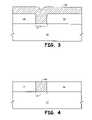
- FIGS. 1–4are cross sections depicting the formation of a cobalt contact plug using an embodiment of the invention
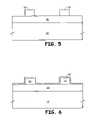
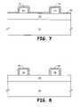
- FIGS. 5–8are cross sections depicting the formation of a self-aligned cobalt silicide structure
- FIG. 9is an isometric depiction of various components which may be manufactured using devices formed with an embodiment of the present invention.
- FIG. 10is a block diagram of an exemplary use of the invention to form part of a memory device having a storage transistor array.
- waferis to be understood as a semiconductor-based material including silicon, silicon-on-insulator (SOI) or silicon-on-sapphire (SOS) technology, doped and undoped semiconductors, epitaxial layers of silicon supported by a base semiconductor foundation, and other semiconductor structures.
- SOIsilicon-on-insulator
- SOSsilicon-on-sapphire
- doped and undoped semiconductorsepitaxial layers of silicon supported by a base semiconductor foundation, and other semiconductor structures.
- previous process stepsmay have been utilized to form regions or junctions in or over the base semiconductor structure or foundation.
- substrate assemblymay include a wafer with layers including dielectrics and conductors, and features such as transistors, formed thereover, depending on the particular stage of processing.
- the term “on” used with respect to two layers, one “on” the other,means at least some contact between the layers, while “over” means the layers are in close proximity, but possibly with one or more additional intervening layers such that contact is possible but not required. Neither “on” nor “over” implies any directionality as used herein.
- FIGS. 1–4A first exemplary embodiment of an inventive method to form a cobalt layer on a bare silicon surface using atomic layer deposition (ALD) is depicted in FIGS. 1–4 .
- FIG. 1depicts a semiconductor wafer substrate assembly comprising a monocrystalline silicon wafer 10 having a doped region therein 12 to which a cobalt metal contact will be formed.
- FIG. 1further depicts a dielectric layer 14 having an opening therein which exposes doped region 12 . The opening may be formed using a patterned photoresist layer to etch the dielectric. It is likely that the completed FIG. 1 structure will comprise other features necessary for device functionality which are not immediately germane to the present invention and which, for simplicity of explanation, are not depicted or described.
- the dielectric layermay include one or more layers of borophosphosilicate glass (BPSG), an oxide formed using tetraethyl orthosilicate (TEOS), a combination of both, or another oxide such as spun-on glass (SOG).
- BPSGborophosphosilicate glass
- TEOStetraethyl orthosilicate
- SOGspun-on glass
- the FIG. 1 structuremay be formed easily by one of ordinary skill in the art using standard processing techniques.
- the waferis exposed to a deoxidizer such as hydrofluoric acid (HF) diluted about 100:1 with water.
- HFhydrofluoric acid
- This etchant solutionwill remove any native oxide (not depicted) and other contaminants from the bare silicon which forms the surface of doped region 12 .
- Native oxideis known to form to about 12 angstroms ( ⁇ ) depth on bare silicon.
- the wet etchwill also remove about the same amount of material from oxide 14 , but negative effects are negligible.
- HFis an acid such as QEtch II (1% phosphoric acid, H 3 PO 4 , and 39% ammonium fluoride, NH 4 F) which will remove native oxide from bare silicon with minimal damage or contamination to the remainder of the semiconductor wafer substrate assembly. It is also contemplated that a dry etch may be used to remove any native oxide from the silicon surface.
- QEtch II1% phosphoric acid, H 3 PO 4 , and 39% ammonium fluoride, NH 4 F
- the waferAfter exposing the silicon to the etchant to remove native oxide, the wafer is placed into a deposition chamber, or remains in such a chamber from prior processing steps. To prevent furnace hydration or the reformation of native oxide on the bare silicon after exposing the wafer to HF, the wafer must be kept in an inert ambient such as N 2 or the next process act must be initiated within about 15 minutes after etching away native oxide from the bare silicon.
- Titanium nitride precursorsmay have the form Ti(NR 1 R 2 ) x (NR 3 R 4 ) 4-x and Ti(NR 1 R 2 ) 4 , where R 1 through R 4 are organic groups.
- Suitable titanium nitride precursorsinclude tetrakis(dimethylamino) titanium (chemical formula Ti(N(CH 3 ) 2 ) 4 , hereinafter “TDMAT”) and tetrakis(diethylamino) titanium (chemical formula Ti(N(C 2 H 5 ) 2 ) 4 , hereinafter “TDEAT”).
- Tantalum nitride precursorswill typically have the form Ta(NR 1 R 2 ) x (NR 3 R 4 ) 5-x where R 1 through R 4 are organic groups.
- Suitable tantalum nitride precursorsinclude (tert-Butylimino)tris (diethylamino)tantalum(V) (chemical formula C 16 H 39 N 4 Ta, hereinafter “TBDET”) and pentakis (dimethylamino) tantalum(V) (chemical formula Ta(NMe 2 ) 5 , hereinafter “PDMAT” where “Me” is a —CH 3 methyl group). These precursors are available from Sigma-Aldrich Corp. of St. Louis, Mo.
- the selected precursor usedis introduced into the deposition chamber at a flow rate of between about 0.05 sccm and about 500 sccm for a duration of between about 10 milliseconds and about 5 minutes.
- the chamberis maintained at a temperature of between about 200° C. and about 300° C. and a pressure of between about 1 millitorr and about 20 torr.
- Other precursors having the general forms listed abovemay require an expanded chamber temperature range of between about 150° C. and 450° C.
- Exposing the silicon to the tantalum nitride (or titanium nitride) precursoris believed to form a thin tantalum (titanium) layer on the surface of the silicon, terminated with dimethylamine groups.
- the chamberAfter exposure of the wafer to TBDET the chamber is purged, for example with N 2 , then ammonia (NH 3 ) is pumped into the chamber at a flow rate of between about 5 sccm and about 5,000 sccm for a duration of between about 1 second and about 30 seconds.
- the chamber temperatureis maintained to between about 200° C. and about 300° C. and a pressure of between about 0.1 millitorr and about 20 torr.
- the chamberAfter exposing the wafer to NH 3 , the chamber is again purged, for example with N 2 .
- Precursor/NH 3 cycleThe sequence of exposing the wafer to the tantalum or titanium nitride precursor, purging the chamber, exposing the wafer to NH 3 , and again purging the chamber is referred to herein as a Precursor/NH 3 cycle.
- a Precursor/NH 3 cycleTo maximize bonding of the cobalt layer to the bare silicon, more than one Precursor/NH 3 cycle may be performed, although one cycle is generally sufficient unless testing reveals enhanced benefits to the use of multiple cycles for a specific application.
- CpCo(CO) 2cyclopentadienylcobalt dicarbonyl
- CpCo(CO) 2chemical formula C 5 H 5 Co(CO) 2 , hereinafter “CpCo(CO) 2 ”.
- CpCo(CO) 2is introduced into the deposition chamber at a flow rate of between about 0.05 sccm and about 500 sccm for a duration of about 10 milliseconds and about 5 minutes.
- the CpCo(CO) 2may be introduced through an inert carrier gas at a flow rate of between about 0 sccm and about 5,000 sccm.
- a reducersuch as hydrogen (H 2 ) or NH 3 is introduced into the chamber at a flow rate of between about 5 sccm and 10,000 sccm for between about 0.01 seconds to about 50 minutes.
- H 2 or NH 3reduces the cobalt precursor layer formed on the silicon surface to pure cobalt metal. While the mechanism has not been studied, exposing the adsorbed cobalt precursor to NH 3 is believed to remove the organic ligand to yield metallic cobalt.
- the surface termination of the bare siliconis altered and so that it accepts bonding with the cobalt precursor.
- exposure of bare silicon to CpCo(CO) 2does not result the bonding between the silicon surface and the cobalt precursor.
- a layer of adsorbed cobalt precursorremains on the silicon surface.
- the structure of FIG. 2remains, including an ALD cobalt layer 20 on the bare silicon and the dielectric layer 14 . As this is an atomic layer, it forms a uniform conformal cobalt layer a single atom thick.
- the cobalt metalwill likely form as an incomplete layer covering about 1 ⁇ 3 of the exposed surface after the initial layer of cobalt metal is formed.
- ALD cobalt metal formationmay be continued by alternating exposure of the cobalt metal layer to CpCo(CO) 2 , then exposing the cobalt precursor which is adsorbed to the cobalt metal to H 2 or NH 3 to reduce the cobalt precursor to metal.
- the chamber temperature and pressureis maintained at the above-stated values during CpCo(CO) 2 exposure and during exposure to the H 2 or NH 3 reducer.
- This cycling of CpCo(CO) 2 /NH 3is performed until a cobalt layer of desired thickness is formed, for example as depicted in FIG. 3 which comprises a cobalt layer 30 which completely fills the opening in dielectric 14 .
- a planarizationsuch as chemical mechanical planarization (CMP) or other abrasive planarization may be performed to remove the cobalt from the horizontal surface of dielectric 14 to result in the cobalt plug 40 of FIG. 4 .
- Wafer processingmay then continue according to means known in the art to form a completed semiconductor device.
- CMPchemical mechanical planarization
- other abrasive planarizationmay be performed to remove the cobalt from the horizontal surface of dielectric 14 to result in the cobalt plug 40 of FIG. 4 .
- Wafer processingmay then continue according to means known in the art to form a completed semiconductor device.
- FIGS. 5–8A second exemplary embodiment of the invention is depicted in FIGS. 5–8 in formation of a self-aligned silicide (i.e. “salicide”) ALD conductive enhancement layer over a polysilicon feature.
- FIG. 5depicts a semiconductor wafer 10 having a dielectric layer 50 , such as a gate oxide or a thicker deposited oxide layer, formed over the semiconductor wafer 10 .
- a dielectric layer 50such as a gate oxide or a thicker deposited oxide layer, formed over the semiconductor wafer 10 .
- One or more silicon features, such as polysilicon interconnects, transistor gates, etc.may be formed on the dielectric layer 50 according to means known in the art. It is likely that the completed FIG. 5 structure will comprise other features necessary for device functionality which are not immediately germane to the present invention and which, for simplicity of explanation, are not depicted or described.
- any native oxideis removed from the polysilicon features 52 , for example by exposure to one of the previously mentioned HF or QEtch II etching solutions. Then, the polysilicon features are exposed to one or more Precursor/NH 3 cycles using the conditions described above for the first embodiment of FIGS. 1–4 . This sequence treats the polysilicon features 52 such that the features will accept bonding with a cobalt precursor.
- the wafer surfaceUpon completion of exposure of the wafer to one or more Precursor/NH 3 cycles, the wafer surface, specifically the polysilicon features 52 , is exposed to CpCo(CO) 2 using the conditions described above for the first embodiment, then the structure is exposed to a reducer (for example H 2 or NH 3 ).
- a reducerfor example H 2 or NH 3 .
- This process sequenceresults in the structure of FIG. 6 , having an ALD cobalt metal layer 60 formed over the wafer surface.
- several additional layers of ALD cobaltare formed on the initial layer by cycling CpCo(CO) 2 /NH 3 until the cobalt layer is between about 5 ⁇ and about 1,000 ⁇ thick.
- the CpCo(CO) 2 /NH 3 cyclesmay be completed between about 5 times and about 1,000 times.
- One exemplary annealmay include increasing the chamber temperature to between about 400° C. to about 600° C., for example about 500° C., for between about 2.5 minutes to 60 minutes, for example about 3 minutes.
- the chamber temperaturemay then be increased to between about 700° C. to about 900° C., for example about 800° C., for between about 20 seconds to about 5 minutes, for example about 30 seconds.
- Pressuremay be maintained to between about 1 torr and about 760 torr, for example 760 torr.
- the unreacted cobalt metal layer 60is etched selective to the cobalt silicide 70 using hydrochloric acid to result in the structure of FIG. 8 , which comprises cobalt salicide layer 80 formed over silicon features 52 . Wafer processing then continues according to techniques known in the art to form a completed semiconductor device.
- the cobalt layermay remain on the wafer as an unreacted cobalt layer.
- the unreacted cobalt metalis as a portion of a digit line contact.
- the inventive cobalt formation processmay be performed subsequent to a gas phase cleaning process of the silicon wafer surface.
- a semiconductor device 90 formed in accordance with the inventionmay be attached along with other devices such as a microprocessor 92 to a printed circuit board 94 , for example to a computer motherboard or as a part of a memory module used in a personal computer, a minicomputer, or a mainframe 96 .
- FIG. 9may also represent use of device 90 in other electronic devices comprising a housing 96 , for example devices comprising a microprocessor 92 , related to telecommunications, the automobile industry, semiconductor test and manufacturing equipment, consumer electronics, or virtually any piece of consumer or industrial electronic equipment.
- FIG. 10is a simplified block diagram of a memory device such as a dynamic random access memory having digit lines and other features which may be formed using an embodiment of the present invention.
- FIG. 10depicts a processor 92 coupled to a memory device 90 , and further depicts the following basic sections of a memory integrated circuit: control circuitry 104 ; row 106 and column 108 address buffers; row 110 and column 112 decoders; sense amplifiers 114 ; memory array 116 ; and data input/output 118 .
Landscapes
- Chemical & Material Sciences (AREA)
- Engineering & Computer Science (AREA)
- General Chemical & Material Sciences (AREA)
- Chemical Kinetics & Catalysis (AREA)
- Materials Engineering (AREA)
- Mechanical Engineering (AREA)
- Metallurgy (AREA)
- Organic Chemistry (AREA)
- Physics & Mathematics (AREA)
- Condensed Matter Physics & Semiconductors (AREA)
- General Physics & Mathematics (AREA)
- Manufacturing & Machinery (AREA)
- Computer Hardware Design (AREA)
- Microelectronics & Electronic Packaging (AREA)
- Power Engineering (AREA)
- Electrodes Of Semiconductors (AREA)
Abstract
Description
Claims (22)
Priority Applications (2)
| Application Number | Priority Date | Filing Date | Title |
|---|---|---|---|
| US11/039,564US7078326B1 (en) | 2005-01-19 | 2005-01-19 | Nucleation method for atomic layer deposition of cobalt on bare silicon during the formation of a semiconductor device |
| US11/488,934US7696624B2 (en) | 2005-01-19 | 2006-07-17 | Nucleation method for atomic layer deposition of cobalt on bare silicon during the formation of a semiconductor device |
Applications Claiming Priority (1)
| Application Number | Priority Date | Filing Date | Title |
|---|---|---|---|
| US11/039,564US7078326B1 (en) | 2005-01-19 | 2005-01-19 | Nucleation method for atomic layer deposition of cobalt on bare silicon during the formation of a semiconductor device |
Related Child Applications (1)
| Application Number | Title | Priority Date | Filing Date |
|---|---|---|---|
| US11/488,934ContinuationUS7696624B2 (en) | 2005-01-19 | 2006-07-17 | Nucleation method for atomic layer deposition of cobalt on bare silicon during the formation of a semiconductor device |
Publications (2)
| Publication Number | Publication Date |
|---|---|
| US7078326B1true US7078326B1 (en) | 2006-07-18 |
| US20060157863A1 US20060157863A1 (en) | 2006-07-20 |
Family
ID=36659073
Family Applications (2)
| Application Number | Title | Priority Date | Filing Date |
|---|---|---|---|
| US11/039,564Expired - LifetimeUS7078326B1 (en) | 2005-01-19 | 2005-01-19 | Nucleation method for atomic layer deposition of cobalt on bare silicon during the formation of a semiconductor device |
| US11/488,934Active2027-04-09US7696624B2 (en) | 2005-01-19 | 2006-07-17 | Nucleation method for atomic layer deposition of cobalt on bare silicon during the formation of a semiconductor device |
Family Applications After (1)
| Application Number | Title | Priority Date | Filing Date |
|---|---|---|---|
| US11/488,934Active2027-04-09US7696624B2 (en) | 2005-01-19 | 2006-07-17 | Nucleation method for atomic layer deposition of cobalt on bare silicon during the formation of a semiconductor device |
Country Status (1)
| Country | Link |
|---|---|
| US (2) | US7078326B1 (en) |
Cited By (3)
| Publication number | Priority date | Publication date | Assignee | Title |
|---|---|---|---|---|
| US20060261479A1 (en)* | 2005-01-19 | 2006-11-23 | Marsh Eugene P | Nucleation method for atomic layer deposition of cobalt on bare silicon during the formation of a semiconductor device |
| CN103081064A (en)* | 2010-09-06 | 2013-05-01 | 株式会社Eugene科技 | Production method for a semiconductor element |
| US10043880B2 (en)* | 2011-04-22 | 2018-08-07 | Asm International N.V. | Metal silicide, metal germanide, methods for making the same |
Families Citing this family (17)
| Publication number | Priority date | Publication date | Assignee | Title |
|---|---|---|---|---|
| KR100852234B1 (en)* | 2006-11-17 | 2008-08-13 | 삼성전자주식회사 | Method of forming a metal oxide layer, method of manufacturing a gate structure, and method of manufacturing a capacitor using the same |
| US7700480B2 (en)* | 2007-04-27 | 2010-04-20 | Micron Technology, Inc. | Methods of titanium deposition |
| US7888248B2 (en)* | 2007-07-13 | 2011-02-15 | Northrop Grumman Systems Corporation | Method of producing large area SiC substrates |
| US8003521B2 (en) | 2009-04-07 | 2011-08-23 | Micron Technology, Inc. | Semiconductor processing |
| US8962876B2 (en) | 2009-05-15 | 2015-02-24 | Wayne State University | Thermally stable volatile film precursors |
| WO2012027357A2 (en) | 2010-08-24 | 2012-03-01 | Wayne State University | Thermally stable volatile precursors |
| US9822446B2 (en) | 2010-08-24 | 2017-11-21 | Wayne State University | Thermally stable volatile precursors |
| TWI550119B (en) | 2010-11-02 | 2016-09-21 | 宇部興產股份有限公司 | (amidoaminoalkane) metal compound and method for producing thin film containing metal using the metal compound |
| DE112012002871T5 (en)* | 2011-07-06 | 2014-03-20 | Wayne State University | Atomic layer deposition of thin films on transition metal |
| US20140073106A1 (en) | 2012-09-12 | 2014-03-13 | International Business Machines Corporation | Lateral bipolar transistor and cmos hybrid technology |
| US8907115B2 (en) | 2012-12-10 | 2014-12-09 | Wayne State University | Synthesis and characterization of first row transition metal complexes containing α-keto hydrazonate ligands as potential precursors for use in metal film deposition |
| US9758866B2 (en) | 2013-02-13 | 2017-09-12 | Wayne State University | Synthesis and characterization of first row transition metal complexes containing α-imino alkoxides as precursors for deposition of metal films |
| US9005704B2 (en)* | 2013-03-06 | 2015-04-14 | Applied Materials, Inc. | Methods for depositing films comprising cobalt and cobalt nitrides |
| US9157149B2 (en) | 2013-06-28 | 2015-10-13 | Wayne State University | Bis(trimethylsilyl) six-membered ring systems and related compounds as reducing agents for forming layers on a substrate |
| US9249505B2 (en) | 2013-06-28 | 2016-02-02 | Wayne State University | Bis(trimethylsilyl) six-membered ring systems and related compounds as reducing agents for forming layers on a substrate |
| US9218980B2 (en)* | 2013-09-13 | 2015-12-22 | Applied Materials, Inc. | Surface treatment to improve CCTBA based CVD co nucleation on dielectric substrate |
| JP2019500495A (en)* | 2015-12-02 | 2019-01-10 | ビーエーエスエフ ソシエタス・ヨーロピアBasf Se | Method for producing thin inorganic film |
Citations (2)
| Publication number | Priority date | Publication date | Assignee | Title |
|---|---|---|---|---|
| US6346477B1 (en)* | 2001-01-09 | 2002-02-12 | Research Foundation Of Suny - New York | Method of interlayer mediated epitaxy of cobalt silicide from low temperature chemical vapor deposition of cobalt |
| US6527855B2 (en)* | 2000-10-10 | 2003-03-04 | Rensselaer Polytechnic Institute | Atomic layer deposition of cobalt from cobalt metallorganic compounds |
Family Cites Families (5)
| Publication number | Priority date | Publication date | Assignee | Title |
|---|---|---|---|---|
| US5047367A (en)* | 1990-06-08 | 1991-09-10 | Intel Corporation | Process for formation of a self aligned titanium nitride/cobalt silicide bilayer |
| EP1292970B1 (en)* | 2000-06-08 | 2011-09-28 | Genitech Inc. | Thin film forming method |
| US6972267B2 (en)* | 2002-03-04 | 2005-12-06 | Applied Materials, Inc. | Sequential deposition of tantalum nitride using a tantalum-containing precursor and a nitrogen-containing precursor |
| US7091131B2 (en)* | 2002-03-21 | 2006-08-15 | Micron Technology, Inc. | Method of forming integrated circuit structures in silicone ladder polymer |
| US7078326B1 (en) | 2005-01-19 | 2006-07-18 | Marsh Eugene P | Nucleation method for atomic layer deposition of cobalt on bare silicon during the formation of a semiconductor device |
- 2005
- 2005-01-19USUS11/039,564patent/US7078326B1/ennot_activeExpired - Lifetime
- 2006
- 2006-07-17USUS11/488,934patent/US7696624B2/enactiveActive
Patent Citations (2)
| Publication number | Priority date | Publication date | Assignee | Title |
|---|---|---|---|---|
| US6527855B2 (en)* | 2000-10-10 | 2003-03-04 | Rensselaer Polytechnic Institute | Atomic layer deposition of cobalt from cobalt metallorganic compounds |
| US6346477B1 (en)* | 2001-01-09 | 2002-02-12 | Research Foundation Of Suny - New York | Method of interlayer mediated epitaxy of cobalt silicide from low temperature chemical vapor deposition of cobalt |
Non-Patent Citations (3)
| Title |
|---|
| "Atomic Layer Deposition of Transition Metals", Lim, et al., Nature Materials, vol. 2, Nov. 2003, pp. 749-754. |
| "Gas Phase Cleaning of Silicon Wafer Surfaces", Anthony J. Muscat, Engineering Research Center for Environmentally Benign Semiconductor Manufacturing. |
| Park et al., "A New ALD-TiN/CoSi2 Contact Plug Process for reliable and Low Defect Density Bit-Line Integration in Sub-Quarter Micron Giga-bit DRAM", Jun. 2002, IEEE 2002 Interconnect technology Conference, pp. 282-284.* |
Cited By (4)
| Publication number | Priority date | Publication date | Assignee | Title |
|---|---|---|---|---|
| US20060261479A1 (en)* | 2005-01-19 | 2006-11-23 | Marsh Eugene P | Nucleation method for atomic layer deposition of cobalt on bare silicon during the formation of a semiconductor device |
| US7696624B2 (en) | 2005-01-19 | 2010-04-13 | Micron Technology, Inc. | Nucleation method for atomic layer deposition of cobalt on bare silicon during the formation of a semiconductor device |
| CN103081064A (en)* | 2010-09-06 | 2013-05-01 | 株式会社Eugene科技 | Production method for a semiconductor element |
| US10043880B2 (en)* | 2011-04-22 | 2018-08-07 | Asm International N.V. | Metal silicide, metal germanide, methods for making the same |
Also Published As
| Publication number | Publication date |
|---|---|
| US20060261479A1 (en) | 2006-11-23 |
| US7696624B2 (en) | 2010-04-13 |
| US20060157863A1 (en) | 2006-07-20 |
Similar Documents
| Publication | Publication Date | Title |
|---|---|---|
| US7696624B2 (en) | Nucleation method for atomic layer deposition of cobalt on bare silicon during the formation of a semiconductor device | |
| TWI781229B (en) | Method for selectively depositing a metallic film on a substrate | |
| US8747960B2 (en) | Processes and systems for engineering a silicon-type surface for selective metal deposition to form a metal silicide | |
| US8241701B2 (en) | Processes and systems for engineering a barrier surface for copper deposition | |
| US8771804B2 (en) | Processes and systems for engineering a copper surface for selective metal deposition | |
| US8053365B2 (en) | Methods for forming all tungsten contacts and lines | |
| US8288275B2 (en) | Method forming contact plug for semiconductor device using H2 remote plasma treatment | |
| US7338908B1 (en) | Method for fabrication of semiconductor interconnect structure with reduced capacitance, leakage current, and improved breakdown voltage | |
| US20030129847A1 (en) | FeRAM sidewall diffusion barrier etch | |
| US20090004848A1 (en) | Method for fabricating interconnection in semiconductor device | |
| JP7343619B2 (en) | Process integrated approach for selective metals by filling | |
| US20040224475A1 (en) | Methods of manufacturing semiconductor devices having a ruthenium layer via atomic layer deposition and associated apparatus and devices | |
| JP2003517716A (en) | Method of forming silicon bonding interface | |
| KR20050116433A (en) | Method of manufacturing semiconductor device | |
| US6815225B2 (en) | Method for forming capacitor of nonvolatile semiconductor memory device | |
| US6514841B2 (en) | Method for manufacturing gate structure for use in semiconductor device | |
| KR20230004821A (en) | Method for Tuning Film Properties of Metal Nitride Using Plasma | |
| US6235632B1 (en) | Tungsten plug formation | |
| US8202810B2 (en) | Low-H plasma treatment with N2 anneal for electronic memory devices | |
| US20050032365A1 (en) | Atomic layer deposition of metal during the formation of a semiconductor device | |
| TW202449902A (en) | Protection layer formation during plasma etching conductive materials | |
| US6020259A (en) | Method of forming a tungsten-plug contact for a semiconductor device | |
| US20040213895A1 (en) | Method of manufacturing multilevel interconnection | |
| US7041597B2 (en) | Semiconductor device having void free contact and method for fabricating the contact | |
| US6319806B1 (en) | Integrated circuit wiring and fabricating method thereof |
Legal Events
| Date | Code | Title | Description |
|---|---|---|---|
| AS | Assignment | Owner name:MICRON TECHNOLOGY, INC., IDAHO Free format text:ASSIGNMENT OF ASSIGNORS INTEREST;ASSIGNOR:MARSH, EUGENE P.;REEL/FRAME:016208/0417 Effective date:20050112 | |
| STCF | Information on status: patent grant | Free format text:PATENTED CASE | |
| FPAY | Fee payment | Year of fee payment:4 | |
| FPAY | Fee payment | Year of fee payment:8 | |
| AS | Assignment | Owner name:U.S. BANK NATIONAL ASSOCIATION, AS COLLATERAL AGENT, CALIFORNIA Free format text:SECURITY INTEREST;ASSIGNOR:MICRON TECHNOLOGY, INC.;REEL/FRAME:038669/0001 Effective date:20160426 Owner name:U.S. BANK NATIONAL ASSOCIATION, AS COLLATERAL AGEN Free format text:SECURITY INTEREST;ASSIGNOR:MICRON TECHNOLOGY, INC.;REEL/FRAME:038669/0001 Effective date:20160426 | |
| AS | Assignment | Owner name:MORGAN STANLEY SENIOR FUNDING, INC., AS COLLATERAL AGENT, MARYLAND Free format text:PATENT SECURITY AGREEMENT;ASSIGNOR:MICRON TECHNOLOGY, INC.;REEL/FRAME:038954/0001 Effective date:20160426 Owner name:MORGAN STANLEY SENIOR FUNDING, INC., AS COLLATERAL Free format text:PATENT SECURITY AGREEMENT;ASSIGNOR:MICRON TECHNOLOGY, INC.;REEL/FRAME:038954/0001 Effective date:20160426 | |
| AS | Assignment | Owner name:U.S. BANK NATIONAL ASSOCIATION, AS COLLATERAL AGENT, CALIFORNIA Free format text:CORRECTIVE ASSIGNMENT TO CORRECT THE REPLACE ERRONEOUSLY FILED PATENT #7358718 WITH THE CORRECT PATENT #7358178 PREVIOUSLY RECORDED ON REEL 038669 FRAME 0001. ASSIGNOR(S) HEREBY CONFIRMS THE SECURITY INTEREST;ASSIGNOR:MICRON TECHNOLOGY, INC.;REEL/FRAME:043079/0001 Effective date:20160426 Owner name:U.S. BANK NATIONAL ASSOCIATION, AS COLLATERAL AGEN Free format text:CORRECTIVE ASSIGNMENT TO CORRECT THE REPLACE ERRONEOUSLY FILED PATENT #7358718 WITH THE CORRECT PATENT #7358178 PREVIOUSLY RECORDED ON REEL 038669 FRAME 0001. ASSIGNOR(S) HEREBY CONFIRMS THE SECURITY INTEREST;ASSIGNOR:MICRON TECHNOLOGY, INC.;REEL/FRAME:043079/0001 Effective date:20160426 | |
| MAFP | Maintenance fee payment | Free format text:PAYMENT OF MAINTENANCE FEE, 12TH YEAR, LARGE ENTITY (ORIGINAL EVENT CODE: M1553) Year of fee payment:12 | |
| AS | Assignment | Owner name:JPMORGAN CHASE BANK, N.A., AS COLLATERAL AGENT, ILLINOIS Free format text:SECURITY INTEREST;ASSIGNORS:MICRON TECHNOLOGY, INC.;MICRON SEMICONDUCTOR PRODUCTS, INC.;REEL/FRAME:047540/0001 Effective date:20180703 Owner name:JPMORGAN CHASE BANK, N.A., AS COLLATERAL AGENT, IL Free format text:SECURITY INTEREST;ASSIGNORS:MICRON TECHNOLOGY, INC.;MICRON SEMICONDUCTOR PRODUCTS, INC.;REEL/FRAME:047540/0001 Effective date:20180703 | |
| AS | Assignment | Owner name:MICRON TECHNOLOGY, INC., IDAHO Free format text:RELEASE BY SECURED PARTY;ASSIGNOR:U.S. BANK NATIONAL ASSOCIATION, AS COLLATERAL AGENT;REEL/FRAME:047243/0001 Effective date:20180629 | |
| AS | Assignment | Owner name:MICRON TECHNOLOGY, INC., IDAHO Free format text:RELEASE BY SECURED PARTY;ASSIGNOR:MORGAN STANLEY SENIOR FUNDING, INC., AS COLLATERAL AGENT;REEL/FRAME:050937/0001 Effective date:20190731 | |
| AS | Assignment | Owner name:MICRON SEMICONDUCTOR PRODUCTS, INC., IDAHO Free format text:RELEASE BY SECURED PARTY;ASSIGNOR:JPMORGAN CHASE BANK, N.A., AS COLLATERAL AGENT;REEL/FRAME:051028/0001 Effective date:20190731 Owner name:MICRON TECHNOLOGY, INC., IDAHO Free format text:RELEASE BY SECURED PARTY;ASSIGNOR:JPMORGAN CHASE BANK, N.A., AS COLLATERAL AGENT;REEL/FRAME:051028/0001 Effective date:20190731 |