US7078308B2 - Method and apparatus for removing adjacent conductive and nonconductive materials of a microelectronic substrate - Google Patents
Method and apparatus for removing adjacent conductive and nonconductive materials of a microelectronic substrateDownload PDFInfo
- Publication number
- US7078308B2 US7078308B2US10/230,628US23062802AUS7078308B2US 7078308 B2US7078308 B2US 7078308B2US 23062802 AUS23062802 AUS 23062802AUS 7078308 B2US7078308 B2US 7078308B2
- Authority
- US
- United States
- Prior art keywords
- substrate
- aperture
- external portion
- fill material
- microelectronic substrate
- Prior art date
- Legal status (The legal status is an assumption and is not a legal conclusion. Google has not performed a legal analysis and makes no representation as to the accuracy of the status listed.)
- Expired - Lifetime, expires
Links
Images


Classifications
- H—ELECTRICITY
- H01—ELECTRIC ELEMENTS
- H01L—SEMICONDUCTOR DEVICES NOT COVERED BY CLASS H10
- H01L21/00—Processes or apparatus adapted for the manufacture or treatment of semiconductor or solid state devices or of parts thereof
- H01L21/02—Manufacture or treatment of semiconductor devices or of parts thereof
- H01L21/04—Manufacture or treatment of semiconductor devices or of parts thereof the devices having potential barriers, e.g. a PN junction, depletion layer or carrier concentration layer
- H01L21/18—Manufacture or treatment of semiconductor devices or of parts thereof the devices having potential barriers, e.g. a PN junction, depletion layer or carrier concentration layer the devices having semiconductor bodies comprising elements of Group IV of the Periodic Table or AIIIBV compounds with or without impurities, e.g. doping materials
- H01L21/30—Treatment of semiconductor bodies using processes or apparatus not provided for in groups H01L21/20 - H01L21/26
- H01L21/31—Treatment of semiconductor bodies using processes or apparatus not provided for in groups H01L21/20 - H01L21/26 to form insulating layers thereon, e.g. for masking or by using photolithographic techniques; After treatment of these layers; Selection of materials for these layers
- H01L21/3105—After-treatment
- H01L21/31051—Planarisation of the insulating layers
- H01L21/31053—Planarisation of the insulating layers involving a dielectric removal step
- H—ELECTRICITY
- H01—ELECTRIC ELEMENTS
- H01L—SEMICONDUCTOR DEVICES NOT COVERED BY CLASS H10
- H01L21/00—Processes or apparatus adapted for the manufacture or treatment of semiconductor or solid state devices or of parts thereof
- H01L21/02—Manufacture or treatment of semiconductor devices or of parts thereof
- H01L21/04—Manufacture or treatment of semiconductor devices or of parts thereof the devices having potential barriers, e.g. a PN junction, depletion layer or carrier concentration layer
- H01L21/18—Manufacture or treatment of semiconductor devices or of parts thereof the devices having potential barriers, e.g. a PN junction, depletion layer or carrier concentration layer the devices having semiconductor bodies comprising elements of Group IV of the Periodic Table or AIIIBV compounds with or without impurities, e.g. doping materials
- H01L21/30—Treatment of semiconductor bodies using processes or apparatus not provided for in groups H01L21/20 - H01L21/26
- H01L21/31—Treatment of semiconductor bodies using processes or apparatus not provided for in groups H01L21/20 - H01L21/26 to form insulating layers thereon, e.g. for masking or by using photolithographic techniques; After treatment of these layers; Selection of materials for these layers
- H01L21/3205—Deposition of non-insulating-, e.g. conductive- or resistive-, layers on insulating layers; After-treatment of these layers
- H01L21/321—After treatment
- H01L21/32115—Planarisation
- H01L21/3212—Planarisation by chemical mechanical polishing [CMP]
- H01L21/32125—Planarisation by chemical mechanical polishing [CMP] by simultaneously passing an electrical current, i.e. electrochemical mechanical polishing, e.g. ECMP
- H—ELECTRICITY
- H10—SEMICONDUCTOR DEVICES; ELECTRIC SOLID-STATE DEVICES NOT OTHERWISE PROVIDED FOR
- H10D—INORGANIC ELECTRIC SEMICONDUCTOR DEVICES
- H10D1/00—Resistors, capacitors or inductors
- H10D1/01—Manufacture or treatment
- H10D1/041—Manufacture or treatment of capacitors having no potential barriers
- H10D1/042—Manufacture or treatment of capacitors having no potential barriers using deposition processes to form electrode extensions
- H—ELECTRICITY
- H10—SEMICONDUCTOR DEVICES; ELECTRIC SOLID-STATE DEVICES NOT OTHERWISE PROVIDED FOR
- H10D—INORGANIC ELECTRIC SEMICONDUCTOR DEVICES
- H10D1/00—Resistors, capacitors or inductors
- H10D1/60—Capacitors
- H10D1/68—Capacitors having no potential barriers
- H10D1/692—Electrodes
- H10D1/694—Electrodes comprising noble metals or noble metal oxides
- H—ELECTRICITY
- H10—SEMICONDUCTOR DEVICES; ELECTRIC SOLID-STATE DEVICES NOT OTHERWISE PROVIDED FOR
- H10D—INORGANIC ELECTRIC SEMICONDUCTOR DEVICES
- H10D1/00—Resistors, capacitors or inductors
- H10D1/60—Capacitors
- H10D1/68—Capacitors having no potential barriers
- H10D1/692—Electrodes
- H10D1/711—Electrodes having non-planar surfaces, e.g. formed by texturisation
- H10D1/716—Electrodes having non-planar surfaces, e.g. formed by texturisation having vertical extensions
Definitions
- the present inventionrelates generally to methods and apparatuses for removing adjacent conductive and nonconductive materials of a microelectronic substrate.
- Microelectronic substrates and substrate assembliestypically include a semiconductor material having features, such as memory cells, that are linked with conductive lines.
- the conductive linescan be formed by first forming trenches or other recesses in the semiconductor material and then overlaying a conductive material (such as a metal) in the trenches. The conductive material is then selectively removed to leave conductive lines extending from one feature in the semiconductor material to another.
- One technique for forming microelectronic featuresis to dispose the features in isolated containers within the microelectronic substrate.
- One typical processincludes forming an aperture in a substrate material (such as borophosphosilicate glass or BPSG), coating the microelectronic substrate (including the walls of the aperture) first with a barrier layer and then with a conductive layer, and then overfilling the aperture with a generally nonconductive material, such as a photoresist material.
- the excess photoresist material, conductive layer material, and barrier layer material located external to the apertureare then removed using chemical-mechanical planarization or polishing (CMP).
- CMPchemical-mechanical planarization or polishing
- the capacitoris then disposed within the photoresist material in the aperture and coupled to other features of the microelectronic substrate with an overlying network of vias and lines.
- One drawback with the foregoing container technique for forming capacitorsis that during the CMP process, small particles of the conductive material removed from the conductive layer can become embedded in the photoresist material within the aperture. The embedded conductive material can cause short circuits and/or other defects in the capacitor that is subsequently formed in the aperture, causing the capacitor to fail.
- a method in accordance with one aspect of the inventionincludes forming an aperture in a microelectronic substrate material, disposing a conductive material in the aperture proximate to a wall of the aperture, and disposing a fill material in the aperture proximate to the conductive material.
- the fill materialhas a hardness of about 0.04 GPa or higher, and in another aspect of the invention, the fill material has a hardness of about 6.5 GPa or higher.
- the fill materialcan include a phosphosilicate glass or a spin-on glass.
- a microelectronic feature, such as an electrode,can then be disposed in the aperture.
- a method in accordance with another aspect of the inventionincludes providing a microelectronic substrate having a substrate material defining a substrate material plane, a conductive material proximate to the substrate material, and a generally nonconductive material proximate to the conductive material.
- the conductive materialis accordingly positioned between the substrate material and the generally nonconductive material.
- a portion of the generally nonconductive materialincludes a first external portion projecting beyond the substrate material plane, and a portion of the conductive material includes a second external portion projecting beyond the substrate material plane. At least part of the first external portion extending beyond the second external portion is removed, and the fill material is recessed inwardly toward the substrate material plane. At least part of the second external portion is also removed.
- the first external portioncan be removed via chemical-mechanical polishing, and the second external portion can be removed via electrochemical-mechanical polishing.
- the first external portioncan be recessed until it extends outwardly from the substrate material plane by distance from about 200 ⁇ to about 500 ⁇ .
- FIGS. 1A–1Fschematically illustrate a process for forming features in a microelectronic substrate in accordance with an embodiment of the invention.
- FIG. 2is a partially schematic illustration of an apparatus for carrying out processes in accordance with embodiments of the invention.
- FIG. 3is a partially schematic, isometric view of a portion of the apparatus shown in FIG. 2 in accordance with an embodiment of the invention.
- FIG. 4is a partially schematic, side elevation view of an apparatus for processing a microelectronic substrate in accordance with another embodiment of the invention.
- FIG. 5schematically illustrates a waveform for electrolytically processing a microelectronic substrate in accordance with another embodiment of the invention.
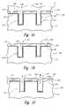
- FIG. 1Ais a partially schematic illustration of a microelectronic substrate 110 positioned for processing in accordance with an embodiment of the invention.
- the microelectronic substrate 110includes a substrate material 111 , such as borophosphosilicate glass (BPSG), and in other embodiments, the microelectronic substrate 110 can include other substrate materials 111 , such as undoped silicon dioxide.
- BPSGborophosphosilicate glass
- one or more apertures 112can be formed in a substrate material plane 113 of the substrate material 111 , using conventional techniques such as patterned etching.
- the apertures 112have a relatively high aspect ratio (i.e., depth-to-width ratio).
- the apertures 112can have an aspect ratio of about 4:1 or more, and in other embodiments, the apertures 112 can have other aspect ratios.
- an underlayer 114(such as tantalum or tantalum oxide) can be disposed on the substrate material plane 113 and adjacent to the walls of the apertures 112 .
- the underlayer 114can be disposed on the microelectronic substrate 110 using conventional techniques, such as physical vapor deposition (PVD) or chemical vapor deposition (CVD).
- PVDphysical vapor deposition
- CVDchemical vapor deposition
- the underlayer 114can form a barrier layer and in other embodiments, the underlayer 114 can perform other functions, such as promoting adhesion of subsequently deposited materials onto the walls of the apertures 112 .
- a layer of conductive material 115is then disposed on the underlayer 114 .
- the conductive material 115can include platinum or platinum alloys, and in other embodiments, the conductive material 115 can include other electrically conductive constituents, such as rhodium, ruthenium, copper or alloys of these materials. Platinum may be particularly suitable for apertures 112 having high aspect ratios, such as aspect ratios of approximately 4:1 or more.
- a fill material 117is then disposed on the conductive material 115 .
- the fill material 117includes subplane portions 118 (positioned beneath the substrate material plane 113 in the apertures 112 ) and a first external portion 119 that extends outwardly away from the substrate material plane 113 , external to the apertures 112 .
- the first external portion 119is disposed on a second external portion 120 defined by the part of the conductive material 115 located external to the apertures 112 and beyond the substrate material plane 113 .
- the fill material 117can include a relatively hard, generally nonconductive substance, such as phosphosilicate glass (PSG).
- the fill material 117can include PSG having 6% phosphorous.
- the fill material 117can include other relatively hard PSG or non-PSG materials, such as spin-on glass (SOG).
- the fill material 117has a hardness greater than that of a typical photoresist material. Accordingly, in one particular embodiment, the fill material 117 can have a hardness of about 0.04 GPa or higher. In one aspect of this embodiment, the hardness is calculated by driving an indenter with a known geometry into the material and measuring the normal applied force as a function of displacement.
- the hardnessis calculated in accordance with other methods.
- the fill material 117includes 6% phosphorous PSG
- the fill material 117can have a hardness of about 6.5 GPa or higher.
- the relatively hard composition of the fill material 117can resist penetration from particles of the conductive material 115 , as described in greater detail below.
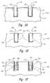
- the first external portion 119 of the fill material 117can be removed (as shown in FIG. 1B ) so that the remaining fill material 117 is flush with the conductive material 115 .
- conventional CMP techniques and slurriesare used to remove the first projection 119 . Apparatuses for removing the first projection 119 are described in greater detail below with reference to FIGS. 2–5 .
- a portion of the remaining fill material 117can be recessed relative to the adjacent conductive material 115 prior to removing the adjacent conductive material 115 .
- the remaining fill material 117can project by distance D 2 (less than D 1 ) from the substrate material plane 113 .
- D 1is approximately 1,000 ⁇
- D 2can be from about 200 ⁇ to about 500 ⁇ .
- the relative values of D 1 and D 2can be different, so long as D 2 is less than D 1 .
- the recess distance(e.g., D 1 minus D 2 ) can be from about 50% to about 80% of D 1 .
- selective etch techniquescan be used to selectively recess the fill material 117 relative to the adjacent second external portion 120 of the conductive material 115 . The second external portion 120 is then removed, as described below.
- FIG. 1Dis a schematic illustration of the microelectronic substrate 110 after the second external portion 120 ( FIG. 1C ) of the conductive material 115 has been removed.
- the second external portion 120can be removed using electrochemical-mechanical polishing (ECMP) techniques and an apparatus generally similar to that described in greater detail below with reference to FIGS. 2–5 .
- ECMPelectrochemical-mechanical polishing
- the removal of the conductive material 115is halted upon exposing the underlayer 114 .
- the conductive material 115is removed more rapidly than is the fill material 117 , so that projections 122 of the fill material 117 extend outwardly from the substrate material plane 113 at the end of this phase of processing.
- the conductive material 115is removed electrolytically, as well as by chemical and/or mechanical action, whereas the generally nonconductive fill material 117 is removed without electrolytic action.
- the projections 122 of the fill material 117are removed in a subsequent step.
- One aspect of an embodiment of the process described above with reference to FIGS. 1C and 1Dis that the fill material 117 is recessed relative to the adjacent conductive material 115 by a selected distance prior to removing the adjacent conductive material 115 .
- One advantage of this processis that recessing the fill material 117 can reduce the likelihood for forming residual deposits of conductive material 115 around the apertures 112 . For example, if the fill material 117 is flush with the second projection 120 (as indicated by distance D 0 in FIG.
- the resulting large mass of fill material 117 extending away from the substrate material plane 113can “shield” the adjacent conductive material 115 and reduce the effectiveness of the ECMP process for removing the conductive material 115 . Accordingly, the process can leave residual deposits 115 a of the conductive material 115 around the apertures 112 , as shown in dashed lines in FIG. 1D . These deposits, if not removed, can cause short-circuits with adjacent structures, and/or can adversely affect subsequent processing steps.
- the fill material 117may not adequately support the conducive material 115 within the apertures 112 during the ECMP and CMP processes, causing the conductive material 115 to shear out of the apertures 112 during processing.
- each container 130includes a volume of fill material 117 surrounded by a layer of conductive material 115 , which is in turn surrounded by the underlayer 114 . At this point, each container 130 is electrically isolated and shielded from the surrounding structures in the microelectronic substrate 110 .
- further featurescan next be disposed in the containers 130 to form structures 121 such as capacitors.
- the featurescan be disposed in the containers 130 using conventional techniques (such as selective etching and deposition) and are electrically coupled to each other and/or to external contacts with a network of vias and/or lines, also formed with conventional techniques, such as damascene techniques.
- the remaining fill material 117 within the apertures 112is removed.
- a film 118formed from a material such as tantalum pentoxide, is then disposed in the apertures 112 , and a conductive electrode 119 is disposed adjacent to the film 118 to form the capacitor.
- the foregoing techniquescan be used to form other features in the microelectronic substrate 110 , such as trenches and/or conductive lines.
- portions of the microelectronic substrate 110can then be diced from the larger wafer of which they are a part for encapsulation and incorporation in electronic devices.
- FIGS. 2–5schematically illustrate apparatuses for processing the microelectronic substrate 110 in a manner generally similar to that described above with reference to FIGS. 1A–1F .
- FIG. 2schematically illustrates an apparatus 260 chemically-mechanically and/or electrochemically-mechanically polishing the microelectronic substrate 110 in accordance with an embodiment of the invention.
- the apparatus 260has a support table 280 with a top-panel 281 at a workstation where an operative portion “W” of a polishing pad 283 is positioned.
- the top-panel 281is generally a rigid plate to provide a flat, solid surface to which a particular section of the polishing pad 283 may be secured during polishing.
- the apparatus 260can also have a plurality of rollers to guide, position and hold the polishing pad 283 over the top-panel 281 .
- the rollerscan include a supply roller 287 , first and second idler rollers 284 a and 284 b , first and second guide rollers 285 a and 285 b , and a take-up roller 286 .
- the supply roller 287carries an unused or preoperative portion of the polishing pad 283
- the take-up roller 286carries a used or postoperative portion of the polishing pad 283 .
- the first idler roller 284 a and the first guide roller 285 acan stretch the polishing pad 283 over the top-panel 281 to hold the polishing pad 283 stationary during operation.
- a motor(not shown) drives at least one of the supply roller 287 and the take-up roller 286 to sequentially advance the polishing pad 283 across the top-panel 281 . Accordingly, clean preoperative sections of the polishing pad 283 may be quickly substituted for used sections to provide a consistent surface for polishing and/or cleaning the microelectronic substrate 110 .
- the apparatus 260can also have a carrier assembly 290 that controls and protects the microelectronic substrate 110 during polishing.
- the carrier assembly 290can include a substrate holder 292 to pick up, hold and release the substrate 110 at appropriate stages of the polishing process.
- the carrier assembly 290can also have a support gantry 294 carrying a drive assembly 295 that can translate along the gantry 294 .
- the drive assembly 295can have an actuator 296 , a drive shaft 297 coupled to the actuator 296 , and an arm 298 projecting from the drive shaft 297 .
- the arm 298carries the substrate holder 292 via a terminal shaft 299 such that the drive assembly 295 orbits the substrate holder 292 about an axis E—E (as indicated by arrow “R 1 ”).
- the terminal shaft 299may also rotate the substrate holder 292 about its central axis F—F (as indicated by arrow “R 2 ”).
- the polishing pad 283 and a polishing liquid 289define a polishing medium 282 that mechanically and/or chemically-mechanically removes material from the surface of the microelectronic substrate 110 .
- the polishing pad 283 used in the apparatus 260can be a fixed-abrasive polishing pad in which abrasive particles are fixedly bonded to a suspension medium. Accordingly, the polishing solution 289 can be a “clean solution” without abrasive particles because the abrasive particles are fixedly distributed across a polishing surface 288 of the polishing pad 283 .
- the polishing pad 283may be a nonabrasive pad without abrasive particles
- the polishing solution 289can be a slurry with abrasive particles and chemicals to remove material from the microelectronic substrate 110 .
- the carrier assembly 290presses the microelectronic substrate 110 against the polishing surface 288 of the polishing pad 283 in the presence of the polishing solution 289 .
- the drive assembly 295then orbits the substrate holder 292 about the axis E—E and optionally rotates the substrate holder 292 about the axis F—F to translate the substrate 110 across the polishing surface 288 .
- the abrasive particles and/or the chemicals in the polishing medium 282remove material from the surface of the microelectronic substrate 110 in a chemical and/or chemical-mechanical polishing process.
- the polishing solution 289can include an electrolyte for ECMP processing.
- the apparatus 260can include an electrolyte supply vessel 230 that delivers an electrolyte separately to the polishing surface 288 of the polishing pad 283 with a conduit 237 , as described in greater detail below with reference to FIG. 3 .
- the apparatus 260can further include a current supply 221 coupled to electrodes positioned proximate to the polishing pad 283 . Accordingly, the apparatus 260 can electrolytically remove material from the microelectronic substrate 110 .
- FIG. 3is a partially exploded, partially schematic isometric view of a portion of the apparatus 260 described above with reference to FIG. 2 .
- the top-panel 281houses a plurality of electrode pairs 370 , each of which includes a first electrode 340 a and a second electrode 340 b .
- the first electrodes 340 aare coupled to a first lead 348 a and the second electrodes 340 b are coupled to a second lead 348 b .
- the first and second leads 348 a and 348 bare coupled to the current supply 241 ( FIG. 2 ).
- the first electrodes 340 acan be separated from the second electrodes 340 b by an electrode dielectric layer 349 a that includes TeflonTM or another suitable dielectric material.
- the electrode dielectric layer 349 acan accordingly control the volume and dielectric constant of the region between the first and second electrodes 340 a and 340 b to control the electrical coupling between the electrodes.
- the electrodes 340 a and 340 bcan be electrically coupled to the microelectronic substrate 110 ( FIG. 2 ) by the polishing pad 283 .
- the polishing pad 283is saturated with an electrolyte 331 supplied by the supply conduits 337 through apertures 338 in the top-panel 281 just beneath the polishing pad 283 .
- the electrodes 320 a and 320 bare selected to be compatible with the electrolyte 331 .
- the electrolyte 331can be supplied to the polishing pad 283 from above (for example, by disposing the electrolyte 331 in the polishing liquid 289 , rather than by directing the electrolyte upwardly through the polishing pad 283 ).
- the apparatus 260can include a pad dielectric layer 349 b ( FIG. 2 ) positioned between the polishing pad 283 and the electrodes 340 a and 340 b .
- the electrodes 340 a and 340 bare isolated from physical contact with the electrolyte 331 and can accordingly be selected from materials that are not necessarily compatible with the electrolyte 331 .
- FIG. 4is an isometric view of a portion of an apparatus 460 having electrodes 440 (shown as a first electrode 440 a and a second electrode 440 b ), and a polishing medium 482 arranged in accordance with another embodiment of the invention.
- the polishing medium 482includes polishing pad portions 483 that project beyond the electrodes 440 a and 440 b .
- Each polishing pad portion 483can include a polishing surface 488 and a plurality of flow passages 484 coupled to a fluid source (not shown in FIG. 4 ) with a conduit 437 .
- Each flow passage 484can have an aperture 485 proximate to the polishing surface 488 to provide an electrolyte 431 proximate to an interface between the microelectronic substrate 110 and the polishing surface 488 .
- the pad portions 483can include recesses 487 surrounding each aperture 485 . Accordingly, the electrolyte 431 can proceed outwardly from the flow passages 484 while the microelectronic substrate 110 is positioned directly overhead and remains spaced apart from the electrodes 420 .
- any of the foregoing apparatuses described above with reference to FIGS. 2–4can be used to chemically-mechanically process the microelectronic substrate 110 , and/or electrochemically-mechanically process the microelectronic substrate 110 .
- the apparatusescan provide a varying electrical current that passes from the electrodes, through the conductive material of the microelectronic substrate 110 , via the electrolytic fluid without contacting the electrodes with the microelectronic substrate 110 .
- the apparatuscan generate a high-frequency wave 504 and can superimpose a low-frequency wave 502 on the high-frequency wave 504 .
- the high-frequency wave 504can include a series of positive or negative voltage spikes contained within a square wave envelope defined by the low-frequency wave 502 .
- Each spike of the high-frequency wave 504can have a relatively steep rise-time slope to transfer charge through the dielectric material to the electrolyte and a more gradual fall-time slope.
- the fall-time slopecan define a straight line, as indicated by high-frequency wave 504 , or a curved line, as indicated by high-frequency wave 504 a .
- the high-frequency wave 504 and the low-frequency wave 502can have other shapes depending, for example, on the particular characteristics of the dielectric material and the electrolyte, the characteristics of the microelectronic substrate 110 , and/or the target rate at which conductive material is to be removed from the microelectronic substrate 110 .
Landscapes
- Engineering & Computer Science (AREA)
- Microelectronics & Electronic Packaging (AREA)
- Condensed Matter Physics & Semiconductors (AREA)
- General Physics & Mathematics (AREA)
- Manufacturing & Machinery (AREA)
- Computer Hardware Design (AREA)
- Physics & Mathematics (AREA)
- Power Engineering (AREA)
- Chemical & Material Sciences (AREA)
- Chemical Kinetics & Catalysis (AREA)
- Electrochemistry (AREA)
- Internal Circuitry In Semiconductor Integrated Circuit Devices (AREA)
- Mechanical Treatment Of Semiconductor (AREA)
- Weting (AREA)
Abstract
Description
Claims (28)
Priority Applications (5)
| Application Number | Priority Date | Filing Date | Title |
|---|---|---|---|
| US10/230,628US7078308B2 (en) | 2002-08-29 | 2002-08-29 | Method and apparatus for removing adjacent conductive and nonconductive materials of a microelectronic substrate |
| US11/413,256US7700436B2 (en) | 2002-08-29 | 2006-04-28 | Method for forming a microelectronic structure having a conductive material and a fill material with a hardness of 0.04 GPA or higher within an aperture |
| US11/413,286US20060208322A1 (en) | 2002-08-29 | 2006-04-28 | Method and apparatus for removing adjacent conductive and non-conductive materials of a microelectronic substrate |
| US12/731,049US8048756B2 (en) | 2002-08-29 | 2010-03-24 | Method for removing metal layers formed outside an aperture of a BPSG layer utilizing multiple etching processes including electrochemical-mechanical polishing |
| US14/281,606US9214359B2 (en) | 2000-08-30 | 2014-05-19 | Method and apparatus for simultaneously removing multiple conductive materials from microelectronic substrates |
Applications Claiming Priority (1)
| Application Number | Priority Date | Filing Date | Title |
|---|---|---|---|
| US10/230,628US7078308B2 (en) | 2002-08-29 | 2002-08-29 | Method and apparatus for removing adjacent conductive and nonconductive materials of a microelectronic substrate |
Related Child Applications (2)
| Application Number | Title | Priority Date | Filing Date |
|---|---|---|---|
| US11/413,256DivisionUS7700436B2 (en) | 2002-08-29 | 2006-04-28 | Method for forming a microelectronic structure having a conductive material and a fill material with a hardness of 0.04 GPA or higher within an aperture |
| US11/413,286DivisionUS20060208322A1 (en) | 2002-08-29 | 2006-04-28 | Method and apparatus for removing adjacent conductive and non-conductive materials of a microelectronic substrate |
Publications (2)
| Publication Number | Publication Date |
|---|---|
| US20040043629A1 US20040043629A1 (en) | 2004-03-04 |
| US7078308B2true US7078308B2 (en) | 2006-07-18 |
Family
ID=31976535
Family Applications (4)
| Application Number | Title | Priority Date | Filing Date |
|---|---|---|---|
| US10/230,628Expired - LifetimeUS7078308B2 (en) | 2000-08-30 | 2002-08-29 | Method and apparatus for removing adjacent conductive and nonconductive materials of a microelectronic substrate |
| US11/413,286AbandonedUS20060208322A1 (en) | 2002-08-29 | 2006-04-28 | Method and apparatus for removing adjacent conductive and non-conductive materials of a microelectronic substrate |
| US11/413,256Expired - LifetimeUS7700436B2 (en) | 2002-08-29 | 2006-04-28 | Method for forming a microelectronic structure having a conductive material and a fill material with a hardness of 0.04 GPA or higher within an aperture |
| US12/731,049Expired - Fee RelatedUS8048756B2 (en) | 2002-08-29 | 2010-03-24 | Method for removing metal layers formed outside an aperture of a BPSG layer utilizing multiple etching processes including electrochemical-mechanical polishing |
Family Applications After (3)
| Application Number | Title | Priority Date | Filing Date |
|---|---|---|---|
| US11/413,286AbandonedUS20060208322A1 (en) | 2002-08-29 | 2006-04-28 | Method and apparatus for removing adjacent conductive and non-conductive materials of a microelectronic substrate |
| US11/413,256Expired - LifetimeUS7700436B2 (en) | 2002-08-29 | 2006-04-28 | Method for forming a microelectronic structure having a conductive material and a fill material with a hardness of 0.04 GPA or higher within an aperture |
| US12/731,049Expired - Fee RelatedUS8048756B2 (en) | 2002-08-29 | 2010-03-24 | Method for removing metal layers formed outside an aperture of a BPSG layer utilizing multiple etching processes including electrochemical-mechanical polishing |
Country Status (1)
| Country | Link |
|---|---|
| US (4) | US7078308B2 (en) |
Cited By (9)
| Publication number | Priority date | Publication date | Assignee | Title |
|---|---|---|---|---|
| US20060199351A1 (en)* | 2002-08-29 | 2006-09-07 | Micron Technology, Inc. | Method and apparatus for removing adjacent conductive and non-conductive materials of a microelectronic substrate |
| US20060234604A1 (en)* | 2000-08-30 | 2006-10-19 | Micron Technology, Inc. | Methods and apparatus for electrical, mechanical and/or chemical removal of conductive material from a microelectronic substrate |
| US20060249397A1 (en)* | 2000-08-30 | 2006-11-09 | Micron Technology, Inc. | Methods and apparatus for electrically detecting characteristics of a microelectronic substrate and/or polishing medium |
| US20070037490A1 (en)* | 2000-08-30 | 2007-02-15 | Micron Technology, Inc. | Methods and apparatus for selectively removing conductive material from a microelectronic substrate |
| US20070066054A1 (en)* | 2005-09-21 | 2007-03-22 | Uzoh Cyprian E | Method of forming contact layers on substrates |
| US20070111641A1 (en)* | 2000-08-30 | 2007-05-17 | Micron Technology, Inc. | Methods and apparatus for electromechanically and/or electrochemically-mechanically removing conductive material from a microelectronic substrate |
| US20080045009A1 (en)* | 2002-08-29 | 2008-02-21 | Micron Technology, Inc. | Method and apparatus for simultaneously removing multiple conductive materials from microelectronic substrates |
| US20090255806A1 (en)* | 2004-09-01 | 2009-10-15 | Micron Technology, Inc. | Methods and systems for removing materials from microfeature workpieces with organic and/or non-aqueous electrolytic media |
| US20100116685A1 (en)* | 2004-02-20 | 2010-05-13 | Micron Technology, Inc. | Methods and apparatuses for electrochemical-mechanical polishing |
Families Citing this family (13)
| Publication number | Priority date | Publication date | Assignee | Title |
|---|---|---|---|---|
| US7074113B1 (en)* | 2000-08-30 | 2006-07-11 | Micron Technology, Inc. | Methods and apparatus for removing conductive material from a microelectronic substrate |
| US7160176B2 (en)* | 2000-08-30 | 2007-01-09 | Micron Technology, Inc. | Methods and apparatus for electrically and/or chemically-mechanically removing conductive material from a microelectronic substrate |
| US7112122B2 (en)* | 2003-09-17 | 2006-09-26 | Micron Technology, Inc. | Methods and apparatus for removing conductive material from a microelectronic substrate |
| WO2005069372A1 (en)* | 2003-12-18 | 2005-07-28 | International Business Machines Corporation | Carbon nanotube conductor for trench capacitors |
| US20060043534A1 (en)* | 2004-08-26 | 2006-03-02 | Kirby Kyle K | Microfeature dies with porous regions, and associated methods and systems |
| US7619310B2 (en)* | 2006-11-03 | 2009-11-17 | Infineon Technologies Ag | Semiconductor interconnect and method of making same |
| US8772939B2 (en)* | 2008-08-04 | 2014-07-08 | Micron Technology, Inc. | Polishing systems and methods for removing conductive material from microelectronic substrates |
| US8594216B2 (en) | 2010-08-25 | 2013-11-26 | Qualcomm Incorporated | Beamforming feedback options for MU-MIMO |
| US20120255635A1 (en)* | 2011-04-11 | 2012-10-11 | Applied Materials, Inc. | Method and apparatus for refurbishing gas distribution plate surfaces |
| US8896521B2 (en) | 2012-04-24 | 2014-11-25 | Qualcomm Mems Technologies, Inc. | Metal-insulator-metal capacitors on glass substrates |
| US10115671B2 (en) | 2012-08-03 | 2018-10-30 | Snaptrack, Inc. | Incorporation of passives and fine pitch through via for package on package |
| WO2017091482A1 (en)* | 2015-11-23 | 2017-06-01 | Corning Incorporated | Removal of inorganic coatings from glass substrates |
| US9741817B2 (en)* | 2016-01-21 | 2017-08-22 | Tower Semiconductor Ltd. | Method for manufacturing a trench metal insulator metal capacitor |
Citations (118)
| Publication number | Priority date | Publication date | Assignee | Title |
|---|---|---|---|---|
| US2315695A (en) | 1938-11-23 | 1943-04-06 | Battelle Memorial Institute | Method of polishing metals |
| US2516105A (en) | 1945-06-20 | 1950-07-25 | Mateosian Edward Der | Electrolytic polishing of metals |
| US3239439A (en) | 1962-07-09 | 1966-03-08 | Bell Telephone Labor Inc | Electrodeposition of metals |
| US3334210A (en) | 1964-05-22 | 1967-08-01 | Cincinnati Milling Machine Co | Electro-discharge machining fluid and method |
| US4839005A (en) | 1987-05-22 | 1989-06-13 | Kabushiki Kaisha Kobe Seiko Sho | Electrolytic-abrasive polishing method of aluminum surface |
| JPH01241129A (en) | 1988-03-23 | 1989-09-26 | Toshiba Corp | Manufacture of semiconductor device |
| EP0459397A2 (en) | 1990-05-28 | 1991-12-04 | Kabushiki Kaisha Toshiba | Semiconductor device having a trench for device isolation and method of fabricating the same |
| US5098533A (en) | 1991-02-06 | 1992-03-24 | International Business Machines Corp. | Electrolytic method for the etch back of encapsulated copper-Invar-copper core structures |
| US5162248A (en)* | 1992-03-13 | 1992-11-10 | Micron Technology, Inc. | Optimized container stacked capacitor DRAM cell utilizing sacrificial oxide deposition and chemical mechanical polishing |
| US5244534A (en) | 1992-01-24 | 1993-09-14 | Micron Technology, Inc. | Two-step chemical mechanical polishing process for producing flush and protruding tungsten plugs |
| US5300155A (en) | 1992-12-23 | 1994-04-05 | Micron Semiconductor, Inc. | IC chemical mechanical planarization process incorporating slurry temperature control |
| US5344539A (en) | 1992-03-30 | 1994-09-06 | Seiko Instruments Inc. | Electrochemical fine processing apparatus |
| US5562529A (en) | 1992-10-08 | 1996-10-08 | Fujitsu Limited | Apparatus and method for uniformly polishing a wafer |
| US5567300A (en) | 1994-09-02 | 1996-10-22 | Ibm Corporation | Electrochemical metal removal technique for planarization of surfaces |
| US5575885A (en) | 1993-12-14 | 1996-11-19 | Kabushiki Kaisha Toshiba | Copper-based metal polishing solution and method for manufacturing semiconductor device |
| US5618381A (en) | 1992-01-24 | 1997-04-08 | Micron Technology, Inc. | Multiple step method of chemical-mechanical polishing which minimizes dishing |
| US5676587A (en) | 1995-12-06 | 1997-10-14 | International Business Machines Corporation | Selective polish process for titanium, titanium nitride, tantalum and tantalum nitride |
| US5681423A (en) | 1996-06-06 | 1997-10-28 | Micron Technology, Inc. | Semiconductor wafer for improved chemical-mechanical polishing over large area features |
| US5780358A (en) | 1996-04-08 | 1998-07-14 | Chartered Semiconductor Manufacturing Ltd. | Method for chemical-mechanical polish (CMP) planarizing of cooper containing conductor layers |
| US5807165A (en) | 1997-03-26 | 1998-09-15 | International Business Machines Corporation | Method of electrochemical mechanical planarization |
| US5840629A (en) | 1995-12-14 | 1998-11-24 | Sematech, Inc. | Copper chemical mechanical polishing slurry utilizing a chromate oxidant |
| US5843818A (en)* | 1995-12-05 | 1998-12-01 | Samsung Electronics Co., Ltd. | Methods of fabricating ferroelectric capacitors |
| US5846398A (en) | 1996-08-23 | 1998-12-08 | Sematech, Inc. | CMP slurry measurement and control technique |
| US5888866A (en)* | 1998-04-18 | 1999-03-30 | United Microelectronics Corp. | Method for fabricating capacitors of a dynamic random access memory |
| US5897375A (en) | 1997-10-20 | 1999-04-27 | Motorola, Inc. | Chemical mechanical polishing (CMP) slurry for copper and method of use in integrated circuit manufacture |
| US5911619A (en) | 1997-03-26 | 1999-06-15 | International Business Machines Corporation | Apparatus for electrochemical mechanical planarization |
| US5930699A (en) | 1996-11-12 | 1999-07-27 | Ericsson Inc. | Address retrieval system |
| US5934980A (en) | 1997-06-09 | 1999-08-10 | Micron Technology, Inc. | Method of chemical mechanical polishing |
| US5952687A (en) | 1994-09-17 | 1999-09-14 | Kabushiki Kaisha Toshiba | Semiconductor memory device having a trench capacitor with lower electrode inside the trench |
| US5954997A (en) | 1996-12-09 | 1999-09-21 | Cabot Corporation | Chemical mechanical polishing slurry useful for copper substrates |
| US5954975A (en) | 1993-11-03 | 1999-09-21 | Intel Corporation | Slurries for chemical mechanical polishing tungsten films |
| US5972792A (en) | 1996-10-18 | 1999-10-26 | Micron Technology, Inc. | Method for chemical-mechanical planarization of a substrate on a fixed-abrasive polishing pad |
| US5993637A (en) | 1996-12-06 | 1999-11-30 | Canon Kabushiki Kaisha | Electrode structure, electrolytic etching process and apparatus |
| US6001730A (en) | 1997-10-20 | 1999-12-14 | Motorola, Inc. | Chemical mechanical polishing (CMP) slurry for polishing copper interconnects which use tantalum-based barrier layers |
| US6007695A (en) | 1997-09-30 | 1999-12-28 | Candescent Technologies Corporation | Selective removal of material using self-initiated galvanic activity in electrolytic bath |
| US6010964A (en) | 1997-08-20 | 2000-01-04 | Micron Technology, Inc. | Wafer surface treatment methods and systems using electrocapillarity |
| US6024856A (en) | 1997-10-10 | 2000-02-15 | Enthone-Omi, Inc. | Copper metallization of silicon wafers using insoluble anodes |
| US6033953A (en) | 1996-12-27 | 2000-03-07 | Texas Instruments Incorporated | Method for manufacturing dielectric capacitor, dielectric memory device |
| US6039633A (en) | 1998-10-01 | 2000-03-21 | Micron Technology, Inc. | Method and apparatus for mechanical and chemical-mechanical planarization of microelectronic-device substrate assemblies |
| US6051496A (en) | 1998-09-17 | 2000-04-18 | Taiwan Semiconductor Manufacturing Company | Use of stop layer for chemical mechanical polishing of CU damascene |
| US6060386A (en) | 1997-08-21 | 2000-05-09 | Micron Technology, Inc. | Method and apparatus for forming features in holes, trenches and other voids in the manufacturing of microelectronic devices |
| US6060395A (en) | 1996-07-17 | 2000-05-09 | Micron Technology, Inc. | Planarization method using a slurry including a dispersant |
| WO2000026443A2 (en) | 1998-11-03 | 2000-05-11 | Nutool, Inc. | Method and apparatus for electrochemical mechanical deposition |
| US6063306A (en) | 1998-06-26 | 2000-05-16 | Cabot Corporation | Chemical mechanical polishing slurry useful for copper/tantalum substrate |
| WO2000028586A2 (en) | 1998-11-10 | 2000-05-18 | Micron Technology, Inc. | Copper chemical-mechanical polishing process using a fixed abrasive polishing pad and a copper layer chemical-mechanical polishing solution specifically adapted for chemical-mechanical polishing with a fixed abrasive pad |
| US6066559A (en) | 1996-02-02 | 2000-05-23 | Micron Technology, Inc. | Method for forming a semiconductor connection with a top surface having an enlarged recess |
| US6066030A (en) | 1999-03-04 | 2000-05-23 | International Business Machines Corporation | Electroetch and chemical mechanical polishing equipment |
| US6068787A (en) | 1996-11-26 | 2000-05-30 | Cabot Corporation | Composition and slurry useful for metal CMP |
| WO2000032356A1 (en) | 1998-12-01 | 2000-06-08 | Nutool, Inc. | Reverse linear polisher with loadable housing |
| US6083840A (en) | 1998-11-25 | 2000-07-04 | Arch Specialty Chemicals, Inc. | Slurry compositions and method for the chemical-mechanical polishing of copper and copper alloys |
| US6100197A (en) | 1998-10-13 | 2000-08-08 | Nec Corporation | Method of fabricating a semiconductor device |
| US6103096A (en) | 1997-11-12 | 2000-08-15 | International Business Machines Corporation | Apparatus and method for the electrochemical etching of a wafer |
| US6103636A (en) | 1997-08-20 | 2000-08-15 | Micron Technology, Inc. | Method and apparatus for selective removal of material from wafer alignment marks |
| US6115233A (en) | 1996-06-28 | 2000-09-05 | Lsi Logic Corporation | Integrated circuit device having a capacitor with the dielectric peripheral region being greater than the dielectric central region |
| US6117781A (en) | 1999-04-22 | 2000-09-12 | Advanced Micro Devices, Inc. | Optimized trench/via profile for damascene processing |
| US6121152A (en) | 1998-06-11 | 2000-09-19 | Integrated Process Equipment Corporation | Method and apparatus for planarization of metallized semiconductor wafers using a bipolar electrode assembly |
| WO2000059008A2 (en) | 1999-03-30 | 2000-10-05 | Nutool, Inc. | Method and apparatus for forming an electrical contact with a semiconductor substrate |
| WO2000059682A1 (en) | 1999-04-03 | 2000-10-12 | Nutool, Inc. | Method and apparatus for plating and polishing a semiconductor substrate |
| US6132586A (en) | 1998-06-11 | 2000-10-17 | Integrated Process Equipment Corporation | Method and apparatus for non-contact metal plating of semiconductor wafers using a bipolar electrode assembly |
| US6143155A (en) | 1998-06-11 | 2000-11-07 | Speedfam Ipec Corp. | Method for simultaneous non-contact electrochemical plating and planarizing of semiconductor wafers using a bipiolar electrode assembly |
| US6162681A (en)* | 1998-01-26 | 2000-12-19 | Texas Instruments - Acer Incorporated | DRAM cell with a fork-shaped capacitor |
| US6171467B1 (en) | 1997-11-25 | 2001-01-09 | The John Hopkins University | Electrochemical-control of abrasive polishing and machining rates |
| US6174425B1 (en) | 1997-05-14 | 2001-01-16 | Motorola, Inc. | Process for depositing a layer of material over a substrate |
| US6180947B1 (en) | 1998-08-07 | 2001-01-30 | Nikon Corporation | Multi-element deflection aberration correction for electron beam lithography |
| US6187651B1 (en) | 1998-05-07 | 2001-02-13 | Samsung Electronics Co., Ltd. | Methods of forming trench isolation regions using preferred stress relieving layers and techniques to inhibit the occurrence of voids |
| US6190494B1 (en) | 1998-07-29 | 2001-02-20 | Micron Technology, Inc. | Method and apparatus for electrically endpointing a chemical-mechanical planarization process |
| US6197182B1 (en) | 1999-07-07 | 2001-03-06 | Technic Inc. | Apparatus and method for plating wafers, substrates and other articles |
| US6196899B1 (en) | 1999-06-21 | 2001-03-06 | Micron Technology, Inc. | Polishing apparatus |
| US6206756B1 (en) | 1998-11-10 | 2001-03-27 | Micron Technology, Inc. | Tungsten chemical-mechanical polishing process using a fixed abrasive polishing pad and a tungsten layer chemical-mechanical polishing solution specifically adapted for chemical-mechanical polishing with a fixed abrasive pad |
| US6218309B1 (en) | 1999-06-30 | 2001-04-17 | Lam Research Corporation | Method of achieving top rounding and uniform etch depths while etching shallow trench isolation features |
| US6250994B1 (en) | 1998-10-01 | 2001-06-26 | Micron Technology, Inc. | Methods and apparatuses for mechanical and chemical-mechanical planarization of microelectronic-device substrate assemblies on planarizing pads |
| US6259128B1 (en) | 1999-04-23 | 2001-07-10 | International Business Machines Corporation | Metal-insulator-metal capacitor for copper damascene process and method of forming the same |
| EP1123956A1 (en) | 2000-02-09 | 2001-08-16 | JSR Corporation | Aqueous dispersion for chemical mechanical polishing |
| US6280581B1 (en) | 1998-12-29 | 2001-08-28 | David Cheng | Method and apparatus for electroplating films on semiconductor wafers |
| US6287974B1 (en) | 1999-06-30 | 2001-09-11 | Lam Research Corporation | Method of achieving top rounding and uniform etch depths while etching shallow trench isolation features |
| US20010025976A1 (en) | 1998-10-16 | 2001-10-04 | Lee Byoung-Taek | Method for manufacturing a capacitor of a semiconductor device |
| US6299741B1 (en) | 1999-11-29 | 2001-10-09 | Applied Materials, Inc. | Advanced electrolytic polish (AEP) assisted metal wafer planarization method and apparatus |
| US20010036746A1 (en) | 2000-03-09 | 2001-11-01 | Shuzo Sato | Methods of producing and polishing semiconductor device and polishing apparatus |
| US6313038B1 (en) | 2000-04-26 | 2001-11-06 | Micron Technology, Inc. | Method and apparatus for controlling chemical interactions during planarization of microelectronic substrates |
| US6322422B1 (en) | 1999-01-19 | 2001-11-27 | Nec Corporation | Apparatus for accurately measuring local thickness of insulating layer on semiconductor wafer during polishing and polishing system using the same |
| US6328632B1 (en) | 1999-08-31 | 2001-12-11 | Micron Technology, Inc. | Polishing pads and planarizing machines for mechanical and/or chemical-mechanical planarization of microelectronic substrate assemblies |
| US20020025763A1 (en) | 2000-08-30 | 2002-02-28 | Whonchee Lee | Methods and apparatus for electrical, mechanical and/or chemical removal of conductive material from a microelectronic substrate |
| US20020025760A1 (en) | 2000-08-30 | 2002-02-28 | Whonchee Lee | Methods and apparatus for electrically and/or chemically-mechanically removing conductive material from a microelectronic substrate |
| US20020025759A1 (en) | 2000-08-30 | 2002-02-28 | Whonchee Lee | Microelectronic substrate having conductive material with blunt cornered apertures, and associated methods for removing conductive material |
| US6368190B1 (en) | 2000-01-26 | 2002-04-09 | Agere Systems Guardian Corp. | Electrochemical mechanical planarization apparatus and method |
| US6368184B1 (en) | 2000-01-06 | 2002-04-09 | Advanced Micro Devices, Inc. | Apparatus for determining metal CMP endpoint using integrated polishing pad electrodes |
| US6379223B1 (en) | 1999-11-29 | 2002-04-30 | Applied Materials, Inc. | Method and apparatus for electrochemical-mechanical planarization |
| US20020052126A1 (en) | 2000-08-31 | 2002-05-02 | Whonchee Lee | Electro-mechanical polishing of platinum container structure |
| US6395607B1 (en) | 1999-06-09 | 2002-05-28 | Alliedsignal Inc. | Integrated circuit fabrication method for self-aligned copper diffusion barrier |
| US20020070126A1 (en) | 2000-09-19 | 2002-06-13 | Shuzo Sato | Polishing method, polishing apparatus, plating method, and plating apparatus |
| US6416647B1 (en) | 1998-04-21 | 2002-07-09 | Applied Materials, Inc. | Electro-chemical deposition cell for face-up processing of single semiconductor substrates |
| US20020104764A1 (en) | 2000-11-20 | 2002-08-08 | Gautam Banerjee | Electropolishing and chemical mechanical planarization |
| US20020108861A1 (en)* | 2001-02-12 | 2002-08-15 | Ismail Emesh | Method and apparatus for electrochemical planarization of a workpiece |
| US20020115283A1 (en) | 2001-02-20 | 2002-08-22 | Chartered Semiconductor Manufacturing Ltd. | Planarization by selective electro-dissolution |
| US6455370B1 (en)* | 2000-08-16 | 2002-09-24 | Micron Technology, Inc. | Method of patterning noble metals for semiconductor devices by electropolishing |
| US6461911B2 (en)* | 2000-05-26 | 2002-10-08 | Samsung Electronics Co., Ltd. | Semiconductor memory device and fabricating method thereof |
| US6464855B1 (en) | 2000-10-04 | 2002-10-15 | Speedfam-Ipec Corporation | Method and apparatus for electrochemical planarization of a workpiece |
| US20030064669A1 (en) | 2001-09-28 | 2003-04-03 | Basol Bulent M. | Low-force electrochemical mechanical processing method and apparatus |
| US20030109198A1 (en)* | 2000-08-30 | 2003-06-12 | Whonchee Lee | Methods and apparatus for electrically detecting characteristics of a microelectronic substrate and/or polishing medium |
| US6620037B2 (en) | 1998-03-18 | 2003-09-16 | Cabot Microelectronics Corporation | Chemical mechanical polishing slurry useful for copper substrates |
| US20030178320A1 (en) | 2001-03-14 | 2003-09-25 | Applied Materials, Inc. | Method and composition for polishing a substrate |
| US6689258B1 (en) | 2002-04-30 | 2004-02-10 | Advanced Micro Devices, Inc. | Electrochemically generated reactants for chemical mechanical planarization |
| US6693036B1 (en) | 1999-09-07 | 2004-02-17 | Sony Corporation | Method for producing semiconductor device polishing apparatus, and polishing method |
| US20040043705A1 (en)* | 2002-08-29 | 2004-03-04 | Whonchee Lee | Method and apparatus for chemically, mechanically, and/or electrolytically removing material from microelectronic substrates |
| US6722942B1 (en) | 2001-05-21 | 2004-04-20 | Advanced Micro Devices, Inc. | Chemical mechanical polishing with electrochemical control |
| US6753250B1 (en) | 2002-06-12 | 2004-06-22 | Novellus Systems, Inc. | Method of fabricating low dielectric constant dielectric films |
| US6776693B2 (en) | 2001-12-19 | 2004-08-17 | Applied Materials Inc. | Method and apparatus for face-up substrate polishing |
| US6780772B2 (en) | 2001-12-21 | 2004-08-24 | Nutool, Inc. | Method and system to provide electroplanarization of a workpiece with a conducting material layer |
| US20040192052A1 (en) | 2001-01-23 | 2004-09-30 | Shyama Mukherjee | Viscous protective overlayers for planarization of integrated circuits |
| US20040259479A1 (en) | 2003-06-23 | 2004-12-23 | Cabot Microelectronics Corporation | Polishing pad for electrochemical-mechanical polishing |
| US6848970B2 (en) | 2002-09-16 | 2005-02-01 | Applied Materials, Inc. | Process control in electrochemically assisted planarization |
| US6852630B2 (en) | 2001-04-23 | 2005-02-08 | Asm Nutool, Inc. | Electroetching process and system |
| US6867136B2 (en) | 2001-07-20 | 2005-03-15 | Nutool, Inc. | Method for electrochemically processing a workpiece |
| US20050059324A1 (en) | 2003-09-17 | 2005-03-17 | Whonchee Lee | Methods and apparatus for removing conductive material from a microelectronic substrate |
| US6881664B2 (en) | 2001-08-28 | 2005-04-19 | Lsi Logic Corporation | Process for planarizing upper surface of damascene wiring structure for integrated circuit structures |
| US6893328B2 (en) | 2003-04-23 | 2005-05-17 | Rohm And Haas Electronic Materials Cmp Holdings, Inc. | Conductive polishing pad with anode and cathode |
| US20050133379A1 (en) | 1998-12-01 | 2005-06-23 | Basol Bulent M. | System for electropolishing and electrochemical mechanical polishing |
| US20050173260A1 (en) | 2003-03-18 | 2005-08-11 | Basol Bulent M. | System for electrochemical mechanical polishing |
Family Cites Families (53)
| Publication number | Priority date | Publication date | Assignee | Title |
|---|---|---|---|---|
| US653411A (en)* | 1900-04-18 | 1900-07-10 | Frederick C Bostwick | Process of making tobacco-brown wrapping-paper. |
| US697182A (en)* | 1901-05-18 | 1902-04-08 | John F Steckenreiter | Window-chair. |
| US4613417A (en) | 1984-12-28 | 1986-09-23 | At&T Bell Laboratories | Semiconductor etching process |
| JP3153018B2 (en) | 1992-10-08 | 2001-04-03 | 富士通株式会社 | Polishing apparatus and polishing method |
| FR2738813B1 (en)* | 1995-09-15 | 1997-10-17 | Saint Gobain Vitrage | SUBSTRATE WITH PHOTO-CATALYTIC COATING |
| US5800248A (en)* | 1996-04-26 | 1998-09-01 | Ontrak Systems Inc. | Control of chemical-mechanical polishing rate across a substrate surface |
| JP4148547B2 (en) | 1996-09-02 | 2008-09-10 | 株式会社デンソー | Manufacturing method of semiconductor device |
| US6017437A (en)* | 1997-08-22 | 2000-01-25 | Cutek Research, Inc. | Process chamber and method for depositing and/or removing material on a substrate |
| JPH11145273A (en) | 1997-11-07 | 1999-05-28 | Fujitsu Ltd | Method for manufacturing semiconductor device |
| WO1999033612A1 (en)* | 1997-12-26 | 1999-07-08 | Ebara Corporation | Polishing device |
| US6010604A (en)* | 1998-02-04 | 2000-01-04 | Stauffer; John E. | Neural network packing |
| US6395152B1 (en) | 1998-07-09 | 2002-05-28 | Acm Research, Inc. | Methods and apparatus for electropolishing metal interconnections on semiconductor devices |
| US6726823B1 (en)* | 1998-11-28 | 2004-04-27 | Acm Research, Inc. | Methods and apparatus for holding and positioning semiconductor workpieces during electropolishing and/or electroplating of the workpieces |
| US6303956B1 (en)* | 1999-02-26 | 2001-10-16 | Micron Technology, Inc. | Conductive container structures having a dielectric cap |
| JP2000269318A (en) | 1999-03-12 | 2000-09-29 | Toshiba Corp | Semiconductor device and manufacturing method thereof |
| US6632335B2 (en)* | 1999-12-24 | 2003-10-14 | Ebara Corporation | Plating apparatus |
| JP3676958B2 (en)* | 1999-12-28 | 2005-07-27 | 株式会社日立製作所 | Manufacturing method of semiconductor integrated circuit device |
| US6537144B1 (en) | 2000-02-17 | 2003-03-25 | Applied Materials, Inc. | Method and apparatus for enhanced CMP using metals having reductive properties |
| US6482307B2 (en) | 2000-05-12 | 2002-11-19 | Nutool, Inc. | Method of and apparatus for making electrical contact to wafer surface for full-face electroplating or electropolishing |
| US6515493B1 (en)* | 2000-04-12 | 2003-02-04 | Speedfam-Ipec Corporation | Method and apparatus for in-situ endpoint detection using electrical sensors |
| US6433929B1 (en)* | 2000-06-12 | 2002-08-13 | Olympus Optical Co., Ltd. | Scanning optical microscope and method of acquiring image |
| US7153195B2 (en)* | 2000-08-30 | 2006-12-26 | Micron Technology, Inc. | Methods and apparatus for selectively removing conductive material from a microelectronic substrate |
| US7153410B2 (en) | 2000-08-30 | 2006-12-26 | Micron Technology, Inc. | Methods and apparatus for electrochemical-mechanical processing of microelectronic workpieces |
| US7074113B1 (en)* | 2000-08-30 | 2006-07-11 | Micron Technology, Inc. | Methods and apparatus for removing conductive material from a microelectronic substrate |
| US7129160B2 (en)* | 2002-08-29 | 2006-10-31 | Micron Technology, Inc. | Method for simultaneously removing multiple conductive materials from microelectronic substrates |
| US7220166B2 (en) | 2000-08-30 | 2007-05-22 | Micron Technology, Inc. | Methods and apparatus for electromechanically and/or electrochemically-mechanically removing conductive material from a microelectronic substrate |
| US6602117B1 (en) | 2000-08-30 | 2003-08-05 | Micron Technology, Inc. | Slurry for use with fixed-abrasive polishing pads in polishing semiconductor device conductive structures that include copper and tungsten and polishing methods |
| US6551935B1 (en)* | 2000-08-31 | 2003-04-22 | Micron Technology, Inc. | Slurry for use in polishing semiconductor device conductive structures that include copper and tungsten and polishing methods |
| US7078308B2 (en) | 2002-08-29 | 2006-07-18 | Micron Technology, Inc. | Method and apparatus for removing adjacent conductive and nonconductive materials of a microelectronic substrate |
| JP3453352B2 (en) | 2000-09-20 | 2003-10-06 | 株式会社半導体先端テクノロジーズ | Polishing apparatus and polishing method |
| TW516471U (en) | 2000-09-29 | 2003-01-01 | Shuo-Ren Li | Electro-chemistry mechanical polishing mechanism for exterior surface of workpiece |
| JP4644926B2 (en)* | 2000-10-13 | 2011-03-09 | ソニー株式会社 | Semiconductor manufacturing apparatus and semiconductor device manufacturing method |
| KR100368935B1 (en)* | 2000-10-27 | 2003-01-24 | 삼성전자 주식회사 | Method for forming cylinder type storage node in semiconductor device |
| US6722950B1 (en)* | 2000-11-07 | 2004-04-20 | Planar Labs Corporation | Method and apparatus for electrodialytic chemical mechanical polishing and deposition |
| US6977224B2 (en) | 2000-12-28 | 2005-12-20 | Intel Corporation | Method of electroless introduction of interconnect structures |
| JP2002254248A (en)* | 2001-02-28 | 2002-09-10 | Sony Corp | Electrochemical machining device |
| US6811680B2 (en)* | 2001-03-14 | 2004-11-02 | Applied Materials Inc. | Planarization of substrates using electrochemical mechanical polishing |
| US7232514B2 (en)* | 2001-03-14 | 2007-06-19 | Applied Materials, Inc. | Method and composition for polishing a substrate |
| US6899804B2 (en) | 2001-04-10 | 2005-05-31 | Applied Materials, Inc. | Electrolyte composition and treatment for electrolytic chemical mechanical polishing |
| US6572755B2 (en) | 2001-04-11 | 2003-06-03 | Speedfam-Ipec Corporation | Method and apparatus for electrochemically depositing a material onto a workpiece surface |
| CN100398261C (en) | 2001-04-24 | 2008-07-02 | 应用材料有限公司 | Conductive Polishing Parts for Electrochemical Mechanical Polishing |
| EP1407472A4 (en)* | 2001-06-28 | 2009-07-15 | Pollack Lab Inc | Self contained sensing apparatus and system |
| US6705926B2 (en)* | 2001-10-24 | 2004-03-16 | Cabot Microelectronics Corporation | Boron-containing polishing system and method |
| US6951599B2 (en) | 2002-01-22 | 2005-10-04 | Applied Materials, Inc. | Electropolishing of metallic interconnects |
| EP1478708A1 (en) | 2002-02-26 | 2004-11-24 | Applied Materials, Inc. | Method and composition for polishing a substrate |
| US6834378B2 (en)* | 2002-10-03 | 2004-12-21 | International Business Machines Corporation | System on a chip bus with automatic pipeline stage insertion for timing closure |
| US6858124B2 (en) | 2002-12-16 | 2005-02-22 | 3M Innovative Properties Company | Methods for polishing and/or cleaning copper interconnects and/or film and compositions therefor |
| US6884338B2 (en) | 2002-12-16 | 2005-04-26 | 3M Innovative Properties Company | Methods for polishing and/or cleaning copper interconnects and/or film and compositions therefor |
| WO2004072332A1 (en) | 2003-02-12 | 2004-08-26 | Ebara Corporation | Polishing fluid, method of polishing, and polishing apparatus |
| US20050016861A1 (en)* | 2003-07-24 | 2005-01-27 | Thomas Laursen | Method for planarizing a work piece |
| US7153777B2 (en) | 2004-02-20 | 2006-12-26 | Micron Technology, Inc. | Methods and apparatuses for electrochemical-mechanical polishing |
| US7566391B2 (en)* | 2004-09-01 | 2009-07-28 | Micron Technology, Inc. | Methods and systems for removing materials from microfeature workpieces with organic and/or non-aqueous electrolytic media |
| US20060163083A1 (en)* | 2005-01-21 | 2006-07-27 | International Business Machines Corporation | Method and composition for electro-chemical-mechanical polishing |
- 2002
- 2002-08-29USUS10/230,628patent/US7078308B2/ennot_activeExpired - Lifetime
- 2006
- 2006-04-28USUS11/413,286patent/US20060208322A1/ennot_activeAbandoned
- 2006-04-28USUS11/413,256patent/US7700436B2/ennot_activeExpired - Lifetime
- 2010
- 2010-03-24USUS12/731,049patent/US8048756B2/ennot_activeExpired - Fee Related
Patent Citations (132)
| Publication number | Priority date | Publication date | Assignee | Title |
|---|---|---|---|---|
| US2315695A (en) | 1938-11-23 | 1943-04-06 | Battelle Memorial Institute | Method of polishing metals |
| US2516105A (en) | 1945-06-20 | 1950-07-25 | Mateosian Edward Der | Electrolytic polishing of metals |
| US3239439A (en) | 1962-07-09 | 1966-03-08 | Bell Telephone Labor Inc | Electrodeposition of metals |
| US3334210A (en) | 1964-05-22 | 1967-08-01 | Cincinnati Milling Machine Co | Electro-discharge machining fluid and method |
| US4839005A (en) | 1987-05-22 | 1989-06-13 | Kabushiki Kaisha Kobe Seiko Sho | Electrolytic-abrasive polishing method of aluminum surface |
| JPH01241129A (en) | 1988-03-23 | 1989-09-26 | Toshiba Corp | Manufacture of semiconductor device |
| EP0459397A3 (en) | 1990-05-28 | 1994-11-02 | Kabushiki Kaisha Toshiba | Semiconductor device having a trench for device isolation and method of fabricating the same |
| EP0459397A2 (en) | 1990-05-28 | 1991-12-04 | Kabushiki Kaisha Toshiba | Semiconductor device having a trench for device isolation and method of fabricating the same |
| US5098533A (en) | 1991-02-06 | 1992-03-24 | International Business Machines Corp. | Electrolytic method for the etch back of encapsulated copper-Invar-copper core structures |
| US5244534A (en) | 1992-01-24 | 1993-09-14 | Micron Technology, Inc. | Two-step chemical mechanical polishing process for producing flush and protruding tungsten plugs |
| US5618381A (en) | 1992-01-24 | 1997-04-08 | Micron Technology, Inc. | Multiple step method of chemical-mechanical polishing which minimizes dishing |
| US5162248A (en)* | 1992-03-13 | 1992-11-10 | Micron Technology, Inc. | Optimized container stacked capacitor DRAM cell utilizing sacrificial oxide deposition and chemical mechanical polishing |
| US5344539A (en) | 1992-03-30 | 1994-09-06 | Seiko Instruments Inc. | Electrochemical fine processing apparatus |
| US5562529A (en) | 1992-10-08 | 1996-10-08 | Fujitsu Limited | Apparatus and method for uniformly polishing a wafer |
| US5624300A (en) | 1992-10-08 | 1997-04-29 | Fujitsu Limited | Apparatus and method for uniformly polishing a wafer |
| US5300155A (en) | 1992-12-23 | 1994-04-05 | Micron Semiconductor, Inc. | IC chemical mechanical planarization process incorporating slurry temperature control |
| US6046099A (en) | 1993-11-03 | 2000-04-04 | Intel Corporation | Plug or via formation using novel slurries for chemical mechanical polishing |
| US5954975A (en) | 1993-11-03 | 1999-09-21 | Intel Corporation | Slurries for chemical mechanical polishing tungsten films |
| US5575885A (en) | 1993-12-14 | 1996-11-19 | Kabushiki Kaisha Toshiba | Copper-based metal polishing solution and method for manufacturing semiconductor device |
| US5567300A (en) | 1994-09-02 | 1996-10-22 | Ibm Corporation | Electrochemical metal removal technique for planarization of surfaces |
| US5952687A (en) | 1994-09-17 | 1999-09-14 | Kabushiki Kaisha Toshiba | Semiconductor memory device having a trench capacitor with lower electrode inside the trench |
| US5843818A (en)* | 1995-12-05 | 1998-12-01 | Samsung Electronics Co., Ltd. | Methods of fabricating ferroelectric capacitors |
| US5676587A (en) | 1995-12-06 | 1997-10-14 | International Business Machines Corporation | Selective polish process for titanium, titanium nitride, tantalum and tantalum nitride |
| US5840629A (en) | 1995-12-14 | 1998-11-24 | Sematech, Inc. | Copper chemical mechanical polishing slurry utilizing a chromate oxidant |
| US6066559A (en) | 1996-02-02 | 2000-05-23 | Micron Technology, Inc. | Method for forming a semiconductor connection with a top surface having an enlarged recess |
| US5780358A (en) | 1996-04-08 | 1998-07-14 | Chartered Semiconductor Manufacturing Ltd. | Method for chemical-mechanical polish (CMP) planarizing of cooper containing conductor layers |
| US5863307A (en) | 1996-04-08 | 1999-01-26 | Chartered Semiconductor Manufacturing, Ltd. | Method and slurry composition for chemical-mechanical polish (CMP) planarizing of copper containing conductor layers |
| US5681423A (en) | 1996-06-06 | 1997-10-28 | Micron Technology, Inc. | Semiconductor wafer for improved chemical-mechanical polishing over large area features |
| US6115233A (en) | 1996-06-28 | 2000-09-05 | Lsi Logic Corporation | Integrated circuit device having a capacitor with the dielectric peripheral region being greater than the dielectric central region |
| US6060395A (en) | 1996-07-17 | 2000-05-09 | Micron Technology, Inc. | Planarization method using a slurry including a dispersant |
| US5846398A (en) | 1996-08-23 | 1998-12-08 | Sematech, Inc. | CMP slurry measurement and control technique |
| US5972792A (en) | 1996-10-18 | 1999-10-26 | Micron Technology, Inc. | Method for chemical-mechanical planarization of a substrate on a fixed-abrasive polishing pad |
| US5930699A (en) | 1996-11-12 | 1999-07-27 | Ericsson Inc. | Address retrieval system |
| US6068787A (en) | 1996-11-26 | 2000-05-30 | Cabot Corporation | Composition and slurry useful for metal CMP |
| US5993637A (en) | 1996-12-06 | 1999-11-30 | Canon Kabushiki Kaisha | Electrode structure, electrolytic etching process and apparatus |
| US5954997A (en) | 1996-12-09 | 1999-09-21 | Cabot Corporation | Chemical mechanical polishing slurry useful for copper substrates |
| US6033953A (en) | 1996-12-27 | 2000-03-07 | Texas Instruments Incorporated | Method for manufacturing dielectric capacitor, dielectric memory device |
| US5807165A (en) | 1997-03-26 | 1998-09-15 | International Business Machines Corporation | Method of electrochemical mechanical planarization |
| US5911619A (en) | 1997-03-26 | 1999-06-15 | International Business Machines Corporation | Apparatus for electrochemical mechanical planarization |
| US6174425B1 (en) | 1997-05-14 | 2001-01-16 | Motorola, Inc. | Process for depositing a layer of material over a substrate |
| US5934980A (en) | 1997-06-09 | 1999-08-10 | Micron Technology, Inc. | Method of chemical mechanical polishing |
| US6010964A (en) | 1997-08-20 | 2000-01-04 | Micron Technology, Inc. | Wafer surface treatment methods and systems using electrocapillarity |
| US6103636A (en) | 1997-08-20 | 2000-08-15 | Micron Technology, Inc. | Method and apparatus for selective removal of material from wafer alignment marks |
| US6060386A (en) | 1997-08-21 | 2000-05-09 | Micron Technology, Inc. | Method and apparatus for forming features in holes, trenches and other voids in the manufacturing of microelectronic devices |
| US6007695A (en) | 1997-09-30 | 1999-12-28 | Candescent Technologies Corporation | Selective removal of material using self-initiated galvanic activity in electrolytic bath |
| US6024856A (en) | 1997-10-10 | 2000-02-15 | Enthone-Omi, Inc. | Copper metallization of silicon wafers using insoluble anodes |
| US6001730A (en) | 1997-10-20 | 1999-12-14 | Motorola, Inc. | Chemical mechanical polishing (CMP) slurry for polishing copper interconnects which use tantalum-based barrier layers |
| US5897375A (en) | 1997-10-20 | 1999-04-27 | Motorola, Inc. | Chemical mechanical polishing (CMP) slurry for copper and method of use in integrated circuit manufacture |
| US6103096A (en) | 1997-11-12 | 2000-08-15 | International Business Machines Corporation | Apparatus and method for the electrochemical etching of a wafer |
| US6171467B1 (en) | 1997-11-25 | 2001-01-09 | The John Hopkins University | Electrochemical-control of abrasive polishing and machining rates |
| US6162681A (en)* | 1998-01-26 | 2000-12-19 | Texas Instruments - Acer Incorporated | DRAM cell with a fork-shaped capacitor |
| US6620037B2 (en) | 1998-03-18 | 2003-09-16 | Cabot Microelectronics Corporation | Chemical mechanical polishing slurry useful for copper substrates |
| US5888866A (en)* | 1998-04-18 | 1999-03-30 | United Microelectronics Corp. | Method for fabricating capacitors of a dynamic random access memory |
| US6416647B1 (en) | 1998-04-21 | 2002-07-09 | Applied Materials, Inc. | Electro-chemical deposition cell for face-up processing of single semiconductor substrates |
| US6187651B1 (en) | 1998-05-07 | 2001-02-13 | Samsung Electronics Co., Ltd. | Methods of forming trench isolation regions using preferred stress relieving layers and techniques to inhibit the occurrence of voids |
| US6132586A (en) | 1998-06-11 | 2000-10-17 | Integrated Process Equipment Corporation | Method and apparatus for non-contact metal plating of semiconductor wafers using a bipolar electrode assembly |
| US6143155A (en) | 1998-06-11 | 2000-11-07 | Speedfam Ipec Corp. | Method for simultaneous non-contact electrochemical plating and planarizing of semiconductor wafers using a bipiolar electrode assembly |
| US6121152A (en) | 1998-06-11 | 2000-09-19 | Integrated Process Equipment Corporation | Method and apparatus for planarization of metallized semiconductor wafers using a bipolar electrode assembly |
| US6063306A (en) | 1998-06-26 | 2000-05-16 | Cabot Corporation | Chemical mechanical polishing slurry useful for copper/tantalum substrate |
| US6190494B1 (en) | 1998-07-29 | 2001-02-20 | Micron Technology, Inc. | Method and apparatus for electrically endpointing a chemical-mechanical planarization process |
| US6180947B1 (en) | 1998-08-07 | 2001-01-30 | Nikon Corporation | Multi-element deflection aberration correction for electron beam lithography |
| US6051496A (en) | 1998-09-17 | 2000-04-18 | Taiwan Semiconductor Manufacturing Company | Use of stop layer for chemical mechanical polishing of CU damascene |
| US6039633A (en) | 1998-10-01 | 2000-03-21 | Micron Technology, Inc. | Method and apparatus for mechanical and chemical-mechanical planarization of microelectronic-device substrate assemblies |
| US6250994B1 (en) | 1998-10-01 | 2001-06-26 | Micron Technology, Inc. | Methods and apparatuses for mechanical and chemical-mechanical planarization of microelectronic-device substrate assemblies on planarizing pads |
| US6100197A (en) | 1998-10-13 | 2000-08-08 | Nec Corporation | Method of fabricating a semiconductor device |
| US20010025976A1 (en) | 1998-10-16 | 2001-10-04 | Lee Byoung-Taek | Method for manufacturing a capacitor of a semiconductor device |
| WO2000026443A2 (en) | 1998-11-03 | 2000-05-11 | Nutool, Inc. | Method and apparatus for electrochemical mechanical deposition |
| US6176992B1 (en) | 1998-11-03 | 2001-01-23 | Nutool, Inc. | Method and apparatus for electro-chemical mechanical deposition |
| WO2000026443A3 (en) | 1998-11-03 | 2000-10-12 | Nutool Inc | Method and apparatus for electrochemical mechanical deposition |
| US6273786B1 (en) | 1998-11-10 | 2001-08-14 | Micron Technology, Inc. | Tungsten chemical-mechanical polishing process using a fixed abrasive polishing pad and a tungsten layer chemical-mechanical polishing solution specifically adapted for chemical-mechanical polishing with a fixed abrasive pad |
| WO2000028586A2 (en) | 1998-11-10 | 2000-05-18 | Micron Technology, Inc. | Copper chemical-mechanical polishing process using a fixed abrasive polishing pad and a copper layer chemical-mechanical polishing solution specifically adapted for chemical-mechanical polishing with a fixed abrasive pad |
| WO2000028586A3 (en) | 1998-11-10 | 2000-10-12 | Micron Technology Inc | Copper chemical-mechanical polishing process using a fixed abrasive polishing pad and a copper layer chemical-mechanical polishing solution specifically adapted for chemical-mechanical polishing with a fixed abrasive pad |
| US6206756B1 (en) | 1998-11-10 | 2001-03-27 | Micron Technology, Inc. | Tungsten chemical-mechanical polishing process using a fixed abrasive polishing pad and a tungsten layer chemical-mechanical polishing solution specifically adapted for chemical-mechanical polishing with a fixed abrasive pad |
| US6276996B1 (en) | 1998-11-10 | 2001-08-21 | Micron Technology, Inc. | Copper chemical-mechanical polishing process using a fixed abrasive polishing pad and a copper layer chemical-mechanical polishing solution specifically adapted for chemical-mechanical polishing with a fixed abrasive pad |
| US6083840A (en) | 1998-11-25 | 2000-07-04 | Arch Specialty Chemicals, Inc. | Slurry compositions and method for the chemical-mechanical polishing of copper and copper alloys |
| WO2000032356A1 (en) | 1998-12-01 | 2000-06-08 | Nutool, Inc. | Reverse linear polisher with loadable housing |
| US20050133379A1 (en) | 1998-12-01 | 2005-06-23 | Basol Bulent M. | System for electropolishing and electrochemical mechanical polishing |
| US6103628A (en) | 1998-12-01 | 2000-08-15 | Nutool, Inc. | Reverse linear polisher with loadable housing |
| US6280581B1 (en) | 1998-12-29 | 2001-08-28 | David Cheng | Method and apparatus for electroplating films on semiconductor wafers |
| US6322422B1 (en) | 1999-01-19 | 2001-11-27 | Nec Corporation | Apparatus for accurately measuring local thickness of insulating layer on semiconductor wafer during polishing and polishing system using the same |
| US6066030A (en) | 1999-03-04 | 2000-05-23 | International Business Machines Corporation | Electroetch and chemical mechanical polishing equipment |
| WO2000059008A2 (en) | 1999-03-30 | 2000-10-05 | Nutool, Inc. | Method and apparatus for forming an electrical contact with a semiconductor substrate |
| WO2000059008A3 (en) | 1999-03-30 | 2001-02-15 | Nutool Inc | Method and apparatus for forming an electrical contact with a semiconductor substrate |
| WO2000059682A1 (en) | 1999-04-03 | 2000-10-12 | Nutool, Inc. | Method and apparatus for plating and polishing a semiconductor substrate |
| US6117781A (en) | 1999-04-22 | 2000-09-12 | Advanced Micro Devices, Inc. | Optimized trench/via profile for damascene processing |
| US6259128B1 (en) | 1999-04-23 | 2001-07-10 | International Business Machines Corporation | Metal-insulator-metal capacitor for copper damascene process and method of forming the same |
| US6395607B1 (en) | 1999-06-09 | 2002-05-28 | Alliedsignal Inc. | Integrated circuit fabrication method for self-aligned copper diffusion barrier |
| US6504247B2 (en) | 1999-06-09 | 2003-01-07 | Alliedsignal Inc. | Integrated having a self-aligned Cu diffusion barrier |
| US6196899B1 (en) | 1999-06-21 | 2001-03-06 | Micron Technology, Inc. | Polishing apparatus |
| US6218309B1 (en) | 1999-06-30 | 2001-04-17 | Lam Research Corporation | Method of achieving top rounding and uniform etch depths while etching shallow trench isolation features |
| US6287974B1 (en) | 1999-06-30 | 2001-09-11 | Lam Research Corporation | Method of achieving top rounding and uniform etch depths while etching shallow trench isolation features |
| US6197182B1 (en) | 1999-07-07 | 2001-03-06 | Technic Inc. | Apparatus and method for plating wafers, substrates and other articles |
| US6328632B1 (en) | 1999-08-31 | 2001-12-11 | Micron Technology, Inc. | Polishing pads and planarizing machines for mechanical and/or chemical-mechanical planarization of microelectronic substrate assemblies |
| US6693036B1 (en) | 1999-09-07 | 2004-02-17 | Sony Corporation | Method for producing semiconductor device polishing apparatus, and polishing method |
| US6379223B1 (en) | 1999-11-29 | 2002-04-30 | Applied Materials, Inc. | Method and apparatus for electrochemical-mechanical planarization |
| US6299741B1 (en) | 1999-11-29 | 2001-10-09 | Applied Materials, Inc. | Advanced electrolytic polish (AEP) assisted metal wafer planarization method and apparatus |
| US6368184B1 (en) | 2000-01-06 | 2002-04-09 | Advanced Micro Devices, Inc. | Apparatus for determining metal CMP endpoint using integrated polishing pad electrodes |
| US6368190B1 (en) | 2000-01-26 | 2002-04-09 | Agere Systems Guardian Corp. | Electrochemical mechanical planarization apparatus and method |
| EP1123956A1 (en) | 2000-02-09 | 2001-08-16 | JSR Corporation | Aqueous dispersion for chemical mechanical polishing |
| US20010036746A1 (en) | 2000-03-09 | 2001-11-01 | Shuzo Sato | Methods of producing and polishing semiconductor device and polishing apparatus |
| US6313038B1 (en) | 2000-04-26 | 2001-11-06 | Micron Technology, Inc. | Method and apparatus for controlling chemical interactions during planarization of microelectronic substrates |
| US6461911B2 (en)* | 2000-05-26 | 2002-10-08 | Samsung Electronics Co., Ltd. | Semiconductor memory device and fabricating method thereof |
| US6455370B1 (en)* | 2000-08-16 | 2002-09-24 | Micron Technology, Inc. | Method of patterning noble metals for semiconductor devices by electropolishing |
| US20020025760A1 (en) | 2000-08-30 | 2002-02-28 | Whonchee Lee | Methods and apparatus for electrically and/or chemically-mechanically removing conductive material from a microelectronic substrate |
| US20020025763A1 (en) | 2000-08-30 | 2002-02-28 | Whonchee Lee | Methods and apparatus for electrical, mechanical and/or chemical removal of conductive material from a microelectronic substrate |
| US20020025759A1 (en) | 2000-08-30 | 2002-02-28 | Whonchee Lee | Microelectronic substrate having conductive material with blunt cornered apertures, and associated methods for removing conductive material |
| US20030109198A1 (en)* | 2000-08-30 | 2003-06-12 | Whonchee Lee | Methods and apparatus for electrically detecting characteristics of a microelectronic substrate and/or polishing medium |
| US20020052126A1 (en) | 2000-08-31 | 2002-05-02 | Whonchee Lee | Electro-mechanical polishing of platinum container structure |
| US20020070126A1 (en) | 2000-09-19 | 2002-06-13 | Shuzo Sato | Polishing method, polishing apparatus, plating method, and plating apparatus |
| US6464855B1 (en) | 2000-10-04 | 2002-10-15 | Speedfam-Ipec Corporation | Method and apparatus for electrochemical planarization of a workpiece |
| US20020104764A1 (en) | 2000-11-20 | 2002-08-08 | Gautam Banerjee | Electropolishing and chemical mechanical planarization |
| US20040192052A1 (en) | 2001-01-23 | 2004-09-30 | Shyama Mukherjee | Viscous protective overlayers for planarization of integrated circuits |
| US20020108861A1 (en)* | 2001-02-12 | 2002-08-15 | Ismail Emesh | Method and apparatus for electrochemical planarization of a workpiece |
| WO2002064314A1 (en) | 2001-02-12 | 2002-08-22 | Speedfam-Ipec Corporation | Method and apparatus for electrochemical planarization of a workpiece |
| US20020115283A1 (en) | 2001-02-20 | 2002-08-22 | Chartered Semiconductor Manufacturing Ltd. | Planarization by selective electro-dissolution |
| US20030178320A1 (en) | 2001-03-14 | 2003-09-25 | Applied Materials, Inc. | Method and composition for polishing a substrate |
| US6852630B2 (en) | 2001-04-23 | 2005-02-08 | Asm Nutool, Inc. | Electroetching process and system |
| US6722942B1 (en) | 2001-05-21 | 2004-04-20 | Advanced Micro Devices, Inc. | Chemical mechanical polishing with electrochemical control |
| US6867136B2 (en) | 2001-07-20 | 2005-03-15 | Nutool, Inc. | Method for electrochemically processing a workpiece |
| US6881664B2 (en) | 2001-08-28 | 2005-04-19 | Lsi Logic Corporation | Process for planarizing upper surface of damascene wiring structure for integrated circuit structures |
| US20030064669A1 (en) | 2001-09-28 | 2003-04-03 | Basol Bulent M. | Low-force electrochemical mechanical processing method and apparatus |
| US6776693B2 (en) | 2001-12-19 | 2004-08-17 | Applied Materials Inc. | Method and apparatus for face-up substrate polishing |
| US6780772B2 (en) | 2001-12-21 | 2004-08-24 | Nutool, Inc. | Method and system to provide electroplanarization of a workpiece with a conducting material layer |
| US6689258B1 (en) | 2002-04-30 | 2004-02-10 | Advanced Micro Devices, Inc. | Electrochemically generated reactants for chemical mechanical planarization |
| US6753250B1 (en) | 2002-06-12 | 2004-06-22 | Novellus Systems, Inc. | Method of fabricating low dielectric constant dielectric films |
| US20040043705A1 (en)* | 2002-08-29 | 2004-03-04 | Whonchee Lee | Method and apparatus for chemically, mechanically, and/or electrolytically removing material from microelectronic substrates |
| US20050178743A1 (en) | 2002-09-16 | 2005-08-18 | Applied Materials, Inc. | Process control in electrochemically assisted planarization |
| US6848970B2 (en) | 2002-09-16 | 2005-02-01 | Applied Materials, Inc. | Process control in electrochemically assisted planarization |
| US20050173260A1 (en) | 2003-03-18 | 2005-08-11 | Basol Bulent M. | System for electrochemical mechanical polishing |
| US6893328B2 (en) | 2003-04-23 | 2005-05-17 | Rohm And Haas Electronic Materials Cmp Holdings, Inc. | Conductive polishing pad with anode and cathode |
| US20040259479A1 (en) | 2003-06-23 | 2004-12-23 | Cabot Microelectronics Corporation | Polishing pad for electrochemical-mechanical polishing |
| US20050059324A1 (en) | 2003-09-17 | 2005-03-17 | Whonchee Lee | Methods and apparatus for removing conductive material from a microelectronic substrate |
Non-Patent Citations (33)
| Title |
|---|
| Aboaf, J.A. and R. W. Broadie, IBM Technical Disclosure Bulletin, Rounding of Square-Shape Holes in Silicon Wafers, vol. 19, No. 8, p. 3042, Jan. 1977, XP- 002235690, NN 77013042. |
| ATMI, Inc., Internal document, adapted from a presentation at the Semicon West '99 Low Dielectric Materials Technology Conference, San Francisco, California, Jul. 12, 1999, pp. 13-25. |
| Bassous, E., IBM Technical Disclosure Bulletin, Low Temperature Methods for Rounding Silicon Nozzles, Vol. 20, No. 2, Jul. 1977, pp. 810-811, XP-002235692, NN7707810. |
| BERNHARDT, A.F., R.J. CONTOLINI,and S.T. MAYER, "Electrochemical Planarization for Multi-level Metallization of Microcircuitry," CircuiTree, vol. 8, No. 10, pp. 38, 40, 42, 44, 46, and 48, Oct. 1995. |
| BERNHARDT, A.F., R.J. CONTOLINI,and S.T. MAYER, "Electrochemical Planarization for Multi-level Metallization of Microcircuitry," CircuiTree, vol. 8, No. 10, pp. 38, 40, 42, 44, 46, and 48, Oct. 1995. |
| D'Heurle, F. M. and K.C. Park, IBM Technical Disclosure Bulletin, Electrolytic Process for Metal Pattern Generation, vol. 17, No. 1, pp. 271-272, Jun. 1974, XP-002235692, NN 7406271. |
| Frankenthal, R.P. and Eaton, D. H., "Electroetching of Platinum in the Titanium-Platinum-Gold Metallization on Silicon Integrated Circuits," Journal of The Electrochemical Society, Vol. 123, No. 5, pp. 703-706, May 1976, Pennington, New Jersey. |
| HUANG, C.S. et al., "A Novel UV Baking Process to Improve DUV Photoresist Hardness," pp. 135-138, Proceedings of the 1999 International Symposium on VLSI Technology, Systems, and Applications: Proceedings of Technical Papers: Jun. 8-10, 1999, Taipei, Taiwan, Institute of Electrical and Electronics Engineers, Inc., Sep. 1999. |
| HUANG, C.S. et al., "A Novel UV Baking Process to Improve DUV Photoresist Hardness," pp. 135-138, Proceedings of the 1999 International Symposium on VLSI Technology, Systems, and Applications: Proceedings of Technical Papers: Jun. 8-10, 1999, Taipei, Taiwan, Institute of Electrical and Electronics Engineers, Inc., Sep. 1999. |
| JUCHNIEWICZ, R. et al." Influence of Pulsed Current on Platinised Titanium and Tantalum Anode Durability," International Congress on Metallic Corrosion, Proceedings - vol. 3, pp. 449-453, Toronto, Jun. 3-7, 1984. |
| JUCHNIEWICZ, R. et al." Influence of Pulsed Current on Platinised Titanium and Tantalum Anode Durability," International Congress on Metallic Corrosion, Proceedings — vol. 3, pp. 449-453, Toronto, Jun. 3-7, 1984. |
| KONDO, S. et al., "Abrasive-Free Polishing for Copper Damascene Interconnection," Journal of the Electrochemical Society, vol. 147, No. 10, pp. 3907-3913, The Electrochemical Society, Inc., Pennington, New Jersey, 2000. |
| McGRAW-HILL, "Chemical bonding," Concise Encyclopedia of Science & Technology, Fourth Edition, Sybil P. Parker, Editor in Chief, p. 367, McGraw-Hill, New York, New York, 1998. |
| Micro Photonics, Inc. CSM Application Bulletin. Low-load Micro Scratch Tester (MST) for Characterisation of thin polymer films [ online] 3 pages. Retrieved from the Internet on Jul. 25, 2002. <URL: http://www.microphotonics.com/mstABpoly.html>. |
| Micro Photonics, Inc. CSM Application Bulletin. Low-load Micro Scratch Tester (MST) for Characterisation of thin polymer films [ online] 3 pages. Retrieved from the Internet on Jul. 25, 2002. <URL: http://www.microphotonics.com/mstABpoly.html>. |
| Micro Photonics, Inc. CSM Nano Hardness Tester online. 6pages. Retrieved from the internet on Jul. 29, 2002. <URL: http://www.microphotonics.com/nht.html>. |
| PCT International Search Report dated Dec. 1, 2003 for PCT/US03/27181 filed Aug.27,2003 (7pages). |
| PCT International Search Report dated Jul. 10, 2003 for PCT/US03/06373 filed Feb. 28, 2003 (4 pages). |
| PCT International Search Report, International Application Number PCT/US02/19495, Mar. 31, 2003. |
| PCT International Search Report, International Application Number PCT/US02/19496, Apr. 4, 2003. |
| PCT Written opinion dated Jun. 10, 2003 for PCT/US02/19495 filed Jun. 20, 2002 (7 pages). |
| PCT Written opinion dated Jun. 10, 2003 for PCT/US02/19496 filed Jun. 20, 2002 (8 pages). |
| PhysicsWorld. Hard Materials (excerpt of Superhard Superlattices ) [online]. S. Barnett and A. Madan, Physics World, Jan. 1998, Institute of Physics Publishing Ltd., Bristol, United Kingdom. Retrieved from the Internet on Jul. 29, 2002. <URL: http://physicsweb.org/box/world/11/1/11/world-11-1-11-1>. |
| U.S. Appl. No. 09/651,779, filed Aug. 30, 2000, Moore. |
| U.S. Appl. No. 09/651,808, filed Aug. 30, 2000, Chopra et al. |
| U.S. Appl. No. 09/653,392, filed Aug. 31, 2000, Chopra et al. |
| U.S. Appl. No. 09/653,411, filed, Aug. 31, 2000, Lee et al. |
| U.S. Appl. No. 10/090,869, filed Mar. 4, 2002, Moore et al. |
| U.S. Appl. No. 10/230,463, filed Aug. 29, 2002, Lee et al. |
| U.S. Appl. No. 10/230,602, filed Aug. 29, 2002, Chopra. |
| U.S. Appl. No. 10/230,970, filed Aug. 29, 2002, Lee et al. |
| U.S. Appl. No. 10/230,972, filed Aug. 29, 2002, Lee et al. |
| U.S. Appl. No. 10/230,973, filed Aug. 29, 2002, Chopra. |
Cited By (21)
| Publication number | Priority date | Publication date | Assignee | Title |
|---|---|---|---|---|
| US7588677B2 (en) | 2000-08-30 | 2009-09-15 | Micron Technology, Inc. | Methods and apparatus for electrical, mechanical and/or chemical removal of conductive material from a microelectronic substrate |
| US7618528B2 (en) | 2000-08-30 | 2009-11-17 | Micron Technology, Inc. | Methods and apparatus for electromechanically and/or electrochemically-mechanically removing conductive material from a microelectronic substrate |
| US20060249397A1 (en)* | 2000-08-30 | 2006-11-09 | Micron Technology, Inc. | Methods and apparatus for electrically detecting characteristics of a microelectronic substrate and/or polishing medium |
| US20070037490A1 (en)* | 2000-08-30 | 2007-02-15 | Micron Technology, Inc. | Methods and apparatus for selectively removing conductive material from a microelectronic substrate |
| US9214359B2 (en) | 2000-08-30 | 2015-12-15 | Micron Technology, Inc. | Method and apparatus for simultaneously removing multiple conductive materials from microelectronic substrates |
| US20070111641A1 (en)* | 2000-08-30 | 2007-05-17 | Micron Technology, Inc. | Methods and apparatus for electromechanically and/or electrochemically-mechanically removing conductive material from a microelectronic substrate |
| US7560017B2 (en) | 2000-08-30 | 2009-07-14 | Micron Technology, Inc. | Methods and apparatus for electrically detecting characteristics of a microelectronic substrate and/or polishing medium |
| US7604729B2 (en) | 2000-08-30 | 2009-10-20 | Micron Technology, Inc. | Methods and apparatus for selectively removing conductive material from a microelectronic substrate |
| US20060234604A1 (en)* | 2000-08-30 | 2006-10-19 | Micron Technology, Inc. | Methods and apparatus for electrical, mechanical and/or chemical removal of conductive material from a microelectronic substrate |
| US7972485B2 (en) | 2000-08-30 | 2011-07-05 | Round Rock Research, Llc | Methods and apparatus for electromechanically and/or electrochemically-mechanically removing conductive material from a microelectronic substrate |
| US20060199351A1 (en)* | 2002-08-29 | 2006-09-07 | Micron Technology, Inc. | Method and apparatus for removing adjacent conductive and non-conductive materials of a microelectronic substrate |
| US20080045009A1 (en)* | 2002-08-29 | 2008-02-21 | Micron Technology, Inc. | Method and apparatus for simultaneously removing multiple conductive materials from microelectronic substrates |
| US8048756B2 (en) | 2002-08-29 | 2011-11-01 | Micron Technology, Inc. | Method for removing metal layers formed outside an aperture of a BPSG layer utilizing multiple etching processes including electrochemical-mechanical polishing |
| US7700436B2 (en) | 2002-08-29 | 2010-04-20 | Micron Technology, Inc. | Method for forming a microelectronic structure having a conductive material and a fill material with a hardness of 0.04 GPA or higher within an aperture |
| US20100116685A1 (en)* | 2004-02-20 | 2010-05-13 | Micron Technology, Inc. | Methods and apparatuses for electrochemical-mechanical polishing |
| US8101060B2 (en) | 2004-02-20 | 2012-01-24 | Round Rock Research, Llc | Methods and apparatuses for electrochemical-mechanical polishing |
| US20090255806A1 (en)* | 2004-09-01 | 2009-10-15 | Micron Technology, Inc. | Methods and systems for removing materials from microfeature workpieces with organic and/or non-aqueous electrolytic media |
| US8603319B2 (en) | 2004-09-01 | 2013-12-10 | Micron Technology, Inc. | Methods and systems for removing materials from microfeature workpieces with organic and/or non-aqueous electrolytic media |
| US7704880B1 (en) | 2005-09-21 | 2010-04-27 | Novellus Systems, Inc. | Method of forming contact layers on substrates |
| US7416975B2 (en)* | 2005-09-21 | 2008-08-26 | Novellus Systems, Inc. | Method of forming contact layers on substrates |
| US20070066054A1 (en)* | 2005-09-21 | 2007-03-22 | Uzoh Cyprian E | Method of forming contact layers on substrates |
Also Published As
| Publication number | Publication date |
|---|---|
| US20060199351A1 (en) | 2006-09-07 |
| US8048756B2 (en) | 2011-11-01 |
| US20040043629A1 (en) | 2004-03-04 |
| US7700436B2 (en) | 2010-04-20 |
| US20060208322A1 (en) | 2006-09-21 |
| US20100176083A1 (en) | 2010-07-15 |
Similar Documents
| Publication | Publication Date | Title |
|---|---|---|
| US8048756B2 (en) | Method for removing metal layers formed outside an aperture of a BPSG layer utilizing multiple etching processes including electrochemical-mechanical polishing | |
| US7192335B2 (en) | Method and apparatus for chemically, mechanically, and/or electrolytically removing material from microelectronic substrates | |
| US9214359B2 (en) | Method and apparatus for simultaneously removing multiple conductive materials from microelectronic substrates | |
| US8603319B2 (en) | Methods and systems for removing materials from microfeature workpieces with organic and/or non-aqueous electrolytic media | |
| US6306768B1 (en) | Method for planarizing microelectronic substrates having apertures | |
| US20020115283A1 (en) | Planarization by selective electro-dissolution | |
| US6739953B1 (en) | Mechanical stress free processing method | |
| JP2005500687A (en) | Formation of semiconductor structures using a combination of planarization and electropolishing. | |
| US7361582B2 (en) | Method of forming a damascene structure with integrated planar dielectric layers | |
| US20050016861A1 (en) | Method for planarizing a work piece | |
| US9099431B2 (en) | Polishing systems and methods for removing conductive material from microelectronic substrates | |
| US7101471B2 (en) | Method for planar material removal technique using multi-phase process environment | |
| US20030211744A1 (en) | Method for preventing or reducing anodic cu corrosion during cmp | |
| EP1579482A2 (en) | Method and apparatus for planarizing a semiconductor wafer |
Legal Events
| Date | Code | Title | Description |
|---|---|---|---|
| AS | Assignment | Owner name:MICRON TECHNOLOGY, INC., IDAHO Free format text:ASSIGNMENT OF ASSIGNORS INTEREST;ASSIGNORS:LEE, WHONCHEE;BLALOCK, GUY;REEL/FRAME:013244/0963 Effective date:20020829 | |
| AS | Assignment | Owner name:MICRON TECHNOLOGY, INC., IDAHO Free format text:ASSIGNMENT OF ASSIGNORS INTEREST;ASSIGNOR:MEIKLE, SCOTT G.;REEL/FRAME:013737/0528 Effective date:20030131 | |
| FEPP | Fee payment procedure | Free format text:PAYOR NUMBER ASSIGNED (ORIGINAL EVENT CODE: ASPN); ENTITY STATUS OF PATENT OWNER: LARGE ENTITY | |
| STCF | Information on status: patent grant | Free format text:PATENTED CASE | |
| FPAY | Fee payment | Year of fee payment:4 | |
| FPAY | Fee payment | Year of fee payment:8 | |
| AS | Assignment | Owner name:U.S. BANK NATIONAL ASSOCIATION, AS COLLATERAL AGENT, CALIFORNIA Free format text:SECURITY INTEREST;ASSIGNOR:MICRON TECHNOLOGY, INC.;REEL/FRAME:038669/0001 Effective date:20160426 Owner name:U.S. BANK NATIONAL ASSOCIATION, AS COLLATERAL AGEN Free format text:SECURITY INTEREST;ASSIGNOR:MICRON TECHNOLOGY, INC.;REEL/FRAME:038669/0001 Effective date:20160426 | |
| AS | Assignment | Owner name:MORGAN STANLEY SENIOR FUNDING, INC., AS COLLATERAL AGENT, MARYLAND Free format text:PATENT SECURITY AGREEMENT;ASSIGNOR:MICRON TECHNOLOGY, INC.;REEL/FRAME:038954/0001 Effective date:20160426 Owner name:MORGAN STANLEY SENIOR FUNDING, INC., AS COLLATERAL Free format text:PATENT SECURITY AGREEMENT;ASSIGNOR:MICRON TECHNOLOGY, INC.;REEL/FRAME:038954/0001 Effective date:20160426 | |
| AS | Assignment | Owner name:U.S. BANK NATIONAL ASSOCIATION, AS COLLATERAL AGENT, CALIFORNIA Free format text:CORRECTIVE ASSIGNMENT TO CORRECT THE REPLACE ERRONEOUSLY FILED PATENT #7358718 WITH THE CORRECT PATENT #7358178 PREVIOUSLY RECORDED ON REEL 038669 FRAME 0001. ASSIGNOR(S) HEREBY CONFIRMS THE SECURITY INTEREST;ASSIGNOR:MICRON TECHNOLOGY, INC.;REEL/FRAME:043079/0001 Effective date:20160426 Owner name:U.S. BANK NATIONAL ASSOCIATION, AS COLLATERAL AGEN Free format text:CORRECTIVE ASSIGNMENT TO CORRECT THE REPLACE ERRONEOUSLY FILED PATENT #7358718 WITH THE CORRECT PATENT #7358178 PREVIOUSLY RECORDED ON REEL 038669 FRAME 0001. ASSIGNOR(S) HEREBY CONFIRMS THE SECURITY INTEREST;ASSIGNOR:MICRON TECHNOLOGY, INC.;REEL/FRAME:043079/0001 Effective date:20160426 | |
| MAFP | Maintenance fee payment | Free format text:PAYMENT OF MAINTENANCE FEE, 12TH YEAR, LARGE ENTITY (ORIGINAL EVENT CODE: M1553) Year of fee payment:12 | |
| AS | Assignment | Owner name:JPMORGAN CHASE BANK, N.A., AS COLLATERAL AGENT, ILLINOIS Free format text:SECURITY INTEREST;ASSIGNORS:MICRON TECHNOLOGY, INC.;MICRON SEMICONDUCTOR PRODUCTS, INC.;REEL/FRAME:047540/0001 Effective date:20180703 Owner name:JPMORGAN CHASE BANK, N.A., AS COLLATERAL AGENT, IL Free format text:SECURITY INTEREST;ASSIGNORS:MICRON TECHNOLOGY, INC.;MICRON SEMICONDUCTOR PRODUCTS, INC.;REEL/FRAME:047540/0001 Effective date:20180703 | |
| AS | Assignment | Owner name:MICRON TECHNOLOGY, INC., IDAHO Free format text:RELEASE BY SECURED PARTY;ASSIGNOR:U.S. BANK NATIONAL ASSOCIATION, AS COLLATERAL AGENT;REEL/FRAME:047243/0001 Effective date:20180629 | |
| AS | Assignment | Owner name:MICRON TECHNOLOGY, INC., IDAHO Free format text:RELEASE BY SECURED PARTY;ASSIGNOR:MORGAN STANLEY SENIOR FUNDING, INC., AS COLLATERAL AGENT;REEL/FRAME:050937/0001 Effective date:20190731 | |
| AS | Assignment | Owner name:MICRON TECHNOLOGY, INC., IDAHO Free format text:RELEASE BY SECURED PARTY;ASSIGNOR:JPMORGAN CHASE BANK, N.A., AS COLLATERAL AGENT;REEL/FRAME:051028/0001 Effective date:20190731 Owner name:MICRON SEMICONDUCTOR PRODUCTS, INC., IDAHO Free format text:RELEASE BY SECURED PARTY;ASSIGNOR:JPMORGAN CHASE BANK, N.A., AS COLLATERAL AGENT;REEL/FRAME:051028/0001 Effective date:20190731 |