US7078296B2 - Self-aligned trench MOSFETs and methods for making the same - Google Patents
Self-aligned trench MOSFETs and methods for making the sameDownload PDFInfo
- Publication number
- US7078296B2 US7078296B2US10/052,234US5223402AUS7078296B2US 7078296 B2US7078296 B2US 7078296B2US 5223402 AUS5223402 AUS 5223402AUS 7078296 B2US7078296 B2US 7078296B2
- Authority
- US
- United States
- Prior art keywords
- providing
- substrate
- layer
- trench
- dielectric
- Prior art date
- Legal status (The legal status is an assumption and is not a legal conclusion. Google has not performed a legal analysis and makes no representation as to the accuracy of the status listed.)
- Expired - Lifetime
Links
Images


Classifications
- H—ELECTRICITY
- H10—SEMICONDUCTOR DEVICES; ELECTRIC SOLID-STATE DEVICES NOT OTHERWISE PROVIDED FOR
- H10D—INORGANIC ELECTRIC SEMICONDUCTOR DEVICES
- H10D84/00—Integrated devices formed in or on semiconductor substrates that comprise only semiconducting layers, e.g. on Si wafers or on GaAs-on-Si wafers
- H10D84/80—Integrated devices formed in or on semiconductor substrates that comprise only semiconducting layers, e.g. on Si wafers or on GaAs-on-Si wafers characterised by the integration of at least one component covered by groups H10D12/00 or H10D30/00, e.g. integration of IGFETs
- H10D84/82—Integrated devices formed in or on semiconductor substrates that comprise only semiconducting layers, e.g. on Si wafers or on GaAs-on-Si wafers characterised by the integration of at least one component covered by groups H10D12/00 or H10D30/00, e.g. integration of IGFETs of only field-effect components
- H10D84/83—Integrated devices formed in or on semiconductor substrates that comprise only semiconducting layers, e.g. on Si wafers or on GaAs-on-Si wafers characterised by the integration of at least one component covered by groups H10D12/00 or H10D30/00, e.g. integration of IGFETs of only field-effect components of only insulated-gate FETs [IGFET]
- H—ELECTRICITY
- H10—SEMICONDUCTOR DEVICES; ELECTRIC SOLID-STATE DEVICES NOT OTHERWISE PROVIDED FOR
- H10D—INORGANIC ELECTRIC SEMICONDUCTOR DEVICES
- H10D84/00—Integrated devices formed in or on semiconductor substrates that comprise only semiconducting layers, e.g. on Si wafers or on GaAs-on-Si wafers
- H10D84/01—Manufacture or treatment
- H10D84/0123—Integrating together multiple components covered by H10D12/00 or H10D30/00, e.g. integrating multiple IGBTs
- H10D84/0126—Integrating together multiple components covered by H10D12/00 or H10D30/00, e.g. integrating multiple IGBTs the components including insulated gates, e.g. IGFETs
- H10D84/016—Integrating together multiple components covered by H10D12/00 or H10D30/00, e.g. integrating multiple IGBTs the components including insulated gates, e.g. IGFETs the components including vertical IGFETs
- H—ELECTRICITY
- H10—SEMICONDUCTOR DEVICES; ELECTRIC SOLID-STATE DEVICES NOT OTHERWISE PROVIDED FOR
- H10D—INORGANIC ELECTRIC SEMICONDUCTOR DEVICES
- H10D84/00—Integrated devices formed in or on semiconductor substrates that comprise only semiconducting layers, e.g. on Si wafers or on GaAs-on-Si wafers
- H10D84/01—Manufacture or treatment
- H10D84/02—Manufacture or treatment characterised by using material-based technologies
- H10D84/03—Manufacture or treatment characterised by using material-based technologies using Group IV technology, e.g. silicon technology or silicon-carbide [SiC] technology
- H10D84/038—Manufacture or treatment characterised by using material-based technologies using Group IV technology, e.g. silicon technology or silicon-carbide [SiC] technology using silicon technology, e.g. SiGe
Definitions
- the inventiongenerally relates to methods for fabricating integrated circuits (ICs) and semiconductor devices and the resulting structures. More particularly, the invention relates to metal oxide semiconductor field effect transistor (MOSFET) devices and methods for making such devices. Even more particularly, the invention relates to self-aligned trench MOSFET devices and methods for making such devices.
- MOSFETmetal oxide semiconductor field effect transistor
- devicessuch as transistors may be formed on a semiconductor wafer or substrate, which is typically made of silicon.
- MOSFET devicesare widely used in numerous applications, including automotive electronics, disk drives and power supplies. Generally, these devices function as switches, and they are used to connect a power supply to a load. It is important that the resistance of the device be as low as possible when the switch is closed. Otherwise, power is wasted and excessive heat may be generated.
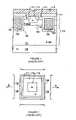
- FIGS. 1 and 2An example of such a device is illustrated in FIGS. 1 and 2 , with FIG. 1 depicting a cross-sectional view of a single cell of a MOSFET 100 , and FIG. 2 depicting a plan view of the cell.
- Gates 102 and 104are formed in trenches and surrounded by gate oxide layers 106 and 108 , respectively.
- the trench gateis often formed in a grid pattern including an array of polygonal shapes (one section of which is shown in FIG. 2 ), the grid representing a single interconnected gate (gates 102 and 104 being the same).
- the trench gatemay also be formed as a series of distinct parallel stripes.
- MOSFET 100is formed in an N-epitaxial layer 110 .
- a N+ source region 112is formed at the surface of epitaxial layer 110 .
- a P+ contact region 114is also formed at the surface of epitaxial layer 110 .
- a P-body region 116is located below N+ source region 112 and P+ contact region 114 .
- a metal source contact 118contacts the source region 112 and shorts the source region 112 to the P+ contact region 114 and P body region 116 .
- the N-epitaxial layer 110is formed on a substrate 120 , and a drain contact (not shown) is located at the bottom of the substrate 120 .
- the contact for the gates 102 and 104is likewise not shown, but it is generally made by extending the conductive gate material outside of the trench and forming a metal contact at a location remote from the individual cells.
- the gateis typically made of phosphorus or boron doped polysilicon.
- a region 111 of N-epitaxial layer 110 between the substrate 120 and the P body 116is generally more lightly doped with N-type impurities than substrate 120 . This increases the ability of MOSFET 100 to withstand high voltages. Region 111 is sometimes referred to as a “lightly doped” or “drift” region (“drift” referring to the movement of carriers in an electric field). Drift region 111 and substrate 120 constitute the drain of MOSFET 100 .
- One feature making the trench configuration attractiveis that the current flows vertically through the channel of the MOSFET. This permits a higher packing density than MOSFETs such as described in U.S. Pat. No. 6,084,268, where the current flows horizontally through the channel and then vertically through the drain. Greater cell density generally means more MOSFETs can be manufactured per unit area of the substrate and, therefore, a lower on-resistance (R DS(on) ) for the device. Increasing the cell density also allows the individual transistors to be closer together, requiring less area on a substrate or wafer and reducing the cost of manufacturing the device.
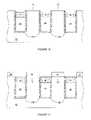
- the alignment toleranceis the amount of over-sizing needed to compensate for variations in the alignment. For example, as illustrated in FIG. 3 , after the gate conductor 10 is placed in the trench 11 , an isolation dielectric 4 is placed over the conductor 10 to electrically isolate the gate conductor from other conductive layers that will be placed on the substrate 12 during subsequent processing. Because the isolation dielectric 4 is only over the gate—and other selected—portions of the device, a masking and etching step using patterned photoresist mask 22 is employed to define the portions of the device where the isolation dielectric 4 need not be present, such as upper surface 13 of substrate 12 .
- the present inventionprovides self-aligned trench MOSFETs and methods for manufacturing the same.
- the self-aligned structure for the MOSFETis provided by making the sidewall of the overlying isolation dielectric layer substantially aligned with the sidewall of the gate conductor. Such an alignment can be made through any number of methods such as using a dual dielectric process, using a selective dielectric oxidation process, using a selective dielectric deposition process, or a spin-on-glass dielectric process.
- FIGS. 1–18are views of one aspect of the MOSFET and method of making the MOSFET according to the invention, in which:
- FIGS. 1 and 2illustrate a prior art MOSFET device
- FIGS. 3–4illustrate how an alignment tolerance occurs during conventional processing
- FIGS. 5–12illustrate the sequence of steps in one aspect of process of the invention
- FIGS. 13 and 14illustrate the cross-sections A and B (respectively) of FIG. 12 ;
- FIGS. 15–16illustrate one aspect of forming an isolation cap according to the invention
- FIG. 17illustrates another aspect of forming an isolation cap according to the invention.
- FIG. 18illustrates yet another aspect of forming an isolation cap according to the invention.
- FIGS. 1–18 presented in conjunction with this descriptionare views of only particular—rather than complete—portions of the MOSFET and method of making the MOSFET according to the invention.
- FIGS. 5–14illustrate one aspect of the process for fabricating a MOSFET in accordance with this invention.
- Other processes resulting in substantially similar structurescan, of course, be used in the invention.
- the processbegins with a substrate 12 .
- Any substrate known in the artcan be used in the invention. Suitable substrates include silicon wafers, epitaxial Si layers, polysilicon layers, bonded wafers such as used in silicon-on-insulator (SOI) technologies, and/or amorphous silicon layers, all of which may be doped or undoped.
- SOIsilicon-on-insulator
- the substrate 12 in the inventionis a single crystal silicon wafer 12 A having at least one epitaxial (“epi”) Si layer 15 located in an upper region thereof. If desired, more than one epitaxial layer can be provided on the upper surface.
- the epitaxial layer(s)can be provided using any known process in the art, including any known epitaxial deposition process.
- the epitaxial layer(s)can remained undoped or can be doped with a desired dopant to the desired concentration using any suitable process known in the art.
- a termination junction 20is formed in an upper region of the epitaxial layer 15 .
- a photoresist layeris deposited and then patterned as known in the art to form a patterned resist layer 23 .
- the patterned resist layer 23is then used as an implant mask during the implantation process used to create the termination junction.
- the implantation processforms a termination implant region 21 by implanting a suitable dopant to obtain the desired profile and concentration. Any dopant known in the art can be employed in the invention depending on the desired type of conductivity, e.g., P or N.
- Suitable dopantsinclude such as arsenic, boron, phosphorus, aluminum, antimony, beryllium, gallium, germanium, gold, magnesium, tellurium, tin, or a combination of these dopants.
- boronis implanted at an energy of about 30 to about 60 KeV with a dopant concentration of about 1 ⁇ 10 14 to about 5 ⁇ 10 15 .
- the resist layeris then stripped using conventional processing, like a wet etch process using hot sulfuric acid and hydrogen peroxide.
- an oxide layer 24is provided over the entire surface of the substrate 12 .
- the oxide layer 24is preferably deposited by heating the substrate 12 in an oxidizing ambient such as oxygen or steam at 900–1100° C.
- the dopant in the termination implant region 21is driven into the substrate to form termination junction 20 to the desired depth, e.g., a depth of about 2,000 to about 10,000 angstroms.
- the dopantis preferably driven by heat treatment in a furnace at a temperature of about 1000 to about 1100 degrees Celsius.
- a field oxide 25is provided from oxide layer 24 .
- the field oxide 25is patterned and etched from the active areas of the device using any known methods in the art.
- a photoresist layercan be deposited and patterned.
- the resulting resist mask 26is then used during an etching process to remove undesired portions of the oxide layer 24 .
- the resist layeris then stripped using conventional processing, like a wet etch process using hot sulfuric acid and hydrogen peroxide.
- Mask 24can comprise either a single layer or multiple layers as known in the art. See, for example, U.S. Pat. Nos. 6,103,635 and 6,121,154, the disclosures of which are incorporated herein by reference.
- mask 24can comprise, for example, any suitable photoresist material. The thickness and other characteristics of the photoresist are well known and can be optimized as known in the art.
- mask 24contains a pattern of openings 31 that expose the upper surface 13 of substrate 12 .
- the openings 31generally correspond to the locations where the trenches 11 will be formed.
- the mask 24is patterned during a photolithographic process as known in the art. The patterning process removes portions of the photoresist material in the location of openings 31 .
- trenches 11are then formed in substrate 12 using any suitable process known in the art.
- the trenchesare formed via a chlorine-based etching process.
- the etching processbegins by forming upper sidewall portions in the epitaxial silicon layer 15 .
- the processthen continues to produce lower sidewall portions and rounded bottom corners.
- the depth of the trenchescan range from about 0.5 to about 3 microns.
- the parameters of the etching processare controlled to preferably form round bottom corners, smooth surfaces, and flat and clean trench bottom surfaces, thereby maintaining the integrity of the MOSFET device characteristics using the trenches.
- the mask 24is removed by any suitable process known in the art, resulting in the structure illustrated in FIG. 9 .
- the photoresist materialcan be removed using a conventional stripping solution such as H 2 SO 4 /H 2 O 2 or an O 2 ash.
- the epitaxial silicon layer 15can be dipped in a diluted acidic solution to remove any polymer and/or passivation present in the trenches. Further cleaning can be performed as known in the art.
- oxide layer 27is then provided on the top surface of the structure, including the trench.
- This oxidewill be used as gate oxide 18 and therefore must be of a high quality.
- Any suitable method known in the art—including oxidation and deposition—yielding a high quality oxide layercan be used to provide oxide layer 27 .
- oxide layer 27is provided by oxidation or deposition.
- the thickness of oxide layer 27can range from about 30 to about 1000 angstroms.
- a conductive layer 28is deposited to fill and overflow the remaining portions of the trench 11 .
- This conductive layer 28can be suitable material that can be used as a gate conductor 10 , such as metal or polysilicon.
- the conductive layeris preferably polysilicon.
- the conductive layer 28can be deposited using any known deposition process, including chemical vapor deposition process.
- the conductive layer 28can be doped with any suitable dopant to the desired concentration.
- the conductor layeris doped with P or B to a concentration of about 5 ⁇ 10 19 by ion implantation or thermal processing.
- Excess (and unneeded) portions of the conductive layer 28are then removed using a photoresist mask 29 to form gate conductor 10 .
- enough of the conductive layer 28is removed so the upper surface 30 of the resulting gate conductor 10 is lower than the upper surface 13 of the substrate 12 .
- the distance between the upper surface 13 of the substrate 12 and the upper surface 30 of the gate conductor 10can range from about 0.25 to about 0.8 microns, and in one aspect of the invention, is preferably about 0.5 microns.
- the excess portions of the conductive layer 28can be removed through any process known in the art, such as a suitable etching process.
- the portions of the oxide layer 27 outside the trenches 11can then be removed through any process known in the art, such as a suitable etching process.
- the photoresist mask 29is stripped as known in the art.
- implant region 32 and channel regions 33are created in an upper region of substrate 12 .
- any suitable doping processthat will obtain the desired profile and concentration can be used to create the implant and channel regions.
- such regionscan be created by implanting P, As, or B at about 30 to about 80 KeV with a dose of about 3 ⁇ 10 13 .
- a maskcan be used to limit the doping process to specific areas of the substrate. Then, the dopant is driven into the substrate by heating for about 20 to about 120 minutes at a temperature of about 1100 degrees Celsius.
- source region 34is created in an upper region of substrate 12 near gates 16 and 17 .
- the source region 34can be created using any suitable doping process that will obtain the desired profile and concentration.
- the source regioncan be created by implanting As, P, or B at about 80 KeV with a dose of about 1 ⁇ 10 16 .
- a source mask 41 made of a suitable photoresist materialis used to limit the doping process to those areas of the substrate where the source region will be created.
- the source maskis removed using any suitable stripping process. Then, the dopant is driven into the substrate by heating for about 60 minutes at a temperature of about 800 to about 1000 degrees Celsius.
- body contact region 35is created in an upper region of substrate 12 and therefore in an upper region of implant region 32 .
- the body contact region 35can be created using any suitable doping process that will obtain the desired profile and concentration.
- the body contact regioncan be created by implanting B, P, or As at about 40–100 KeV with a dose of about 1 ⁇ 10 14 to about 8 ⁇ 10 15 .
- the dopantis driven into the substrate by a standard furnace anneal or a rapid thermal anneal.
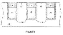
- a self-aligned dielectric layer(or isolation cap 38 ) is provided over gate conductor 10 .
- the isolation capis created in the following manner, the “dual dielectric process.”
- a first dielectric layer 36is provided over the surface of the substrate 12 .
- the first dielectric layercan be provided using any suitable process in the art, such as an oxidation or deposition process like PECVD.
- the first dielectric layer 36can comprise any dielectric material such as PSG, BPSG, or an undoped LTO (low temperature oxide) layer.
- the first dielectric layeris PSG.
- the first dielectric layer 36is doped so that it etches faster than the second dielectric layer 37 (described below).
- the first dielectric layer 36can be doped after it is deposited or while it is being deposited (in situ).
- first dielectric layer 36is made of PSG, it is doped with P to a concentration of about 1 to about 3%.
- a second dielectric layer 37is provided over the surface of the first dielectric layer 36 .
- the second dielectric layer 37can be provided using any suitable process in the art such as a deposition process like PECVD.
- the second dielectric layer 37can comprise any dielectric material such as PSG or BPSG.
- the second dielectric layeris BPSG.
- the second dielectric layer (and accompanying dopant as described below)is also selected so that it reflows more readily than the first dielectric layer 36 .
- the second dielectric layer 37is doped so that it etches shower than the first dielectric layer 36 .
- the second dielectric layercan be doped after it is deposited or while it is being deposited (in situ).
- second dielectric layer 37is made of BPSG, it is doped with B to a concentration of about 3–5% and P to a concentration of about 3–5%.
- both dielectric layersare flowed.
- the flow processwill create a planar upper surface for the dielectric layers, as depicted in FIG. 15 .
- the flow process selectedcan be any known in the art that will create the substantially planar upper surface, like heating for 100 minutes at a temperature of about 850 to about 900 degrees Celsius.
- the first and second dielectric layersare removed to leave an isolation cap 38 in the trench on the gate conductor 10 .
- the dielectric layerscan be removed using any suitable process, such as an isotropic etching process using BOE or anisotropic etching processes such as a dry plasma etch. The etching process removes the dielectric layers from the regions where they need not be present, as well as leaves a substantially planar upper surface of isolation cap 38 .
- a single dielectric layercan be used instead of two dielectric layers.
- the single dielectric layercan be doped or undoped.
- the single dielectric layeris then flowed and isotropically etched in vertical direction until the upper surface of the substrate is exposed.
- the process in this variationleaves an isolation cap in the trench over the gate conductor because the thickness of the reflowed single dielectric layer is greater in the trench than outside the trench and the isotropic etch will remove the same amount of dielectric layer regardless of location.
- the isolation cap 38is provided in an alternative manner, the “selective dielectric oxidation process.”
- the mask 24 used while etching the trenches in the substrate 12is made of nitride.
- a single dielectric layeris grown over the gate conductor 10 .
- the dielectric layer 39is grown by oxidation.
- this dielectric layercan be grown by oxidation in oxygen and hydrogen in a high-temperature oxidation furnace at a temperature of about 900 to about 1100 degrees Celsius for about 30 to about 90 minutes.
- the oxidation processdoes not oxidize portions of the substrate upper surface 13 other than in the trenches 11 .
- the mask 24 containing the nitridecan be removed by any suitable process, such as a wet etch using hot phosphoric acid. With mask 24 removed, isolation cap remains over gate conductor 10 .
- the isolation cap 38is provided in yet another manner, the “selective dielectric deposition process.”
- the mask 24 used while etching the trenches in the substrate 12is again made of nitride.
- a single dielectric layeris grown over the gate conductor 10 .
- the dielectric layeris selectively deposited by any suitable deposition process known in the art.
- the dielectric layercan be deposited by SACVD and then flowing TEOS and ozone in a temperature of about 400 to about 500 degrees Celsius and a pressure ranging from about 200 to about 600 torr, thereby depositing a non-organic silicon dioxide layer containing only residual amounts of carbon atoms.
- the depositionis a selective deposition process, the single dielectric layer is only deposited over gate conductor 10 .
- the mask 24 containing the nitridecan be removed by any suitable process, such as a wet etch using hot phosphoric acid. With mask 24 removed, isolation cap remains over gate conductor 10 .
- the isolation cap 38is provided in still yet another manner, the “SOG dielectric process.”
- an organic dielectric materialsuch as spin-on-glass (SOG) layer is applied to the substrate as known in the art. See, for example, U.S. Pat. No. 6,090,716,the disclosure of which is incorporated herein by reference.
- SOGspin-on-glass
- the SOG layeris applied in such a manner so that the SOG remains in the trenches 11 to form the isolation cap 38 .
- the SOGcan be applied so that it optionally remains on the portion of conductive layer 28 overlying the field oxide.
Landscapes
- Insulated Gate Type Field-Effect Transistor (AREA)
Abstract
Description
Claims (24)
Priority Applications (1)
| Application Number | Priority Date | Filing Date | Title |
|---|---|---|---|
| US10/052,234US7078296B2 (en) | 2002-01-16 | 2002-01-16 | Self-aligned trench MOSFETs and methods for making the same |
Applications Claiming Priority (1)
| Application Number | Priority Date | Filing Date | Title |
|---|---|---|---|
| US10/052,234US7078296B2 (en) | 2002-01-16 | 2002-01-16 | Self-aligned trench MOSFETs and methods for making the same |
Publications (2)
| Publication Number | Publication Date |
|---|---|
| US20030132480A1 US20030132480A1 (en) | 2003-07-17 |
| US7078296B2true US7078296B2 (en) | 2006-07-18 |
Family
ID=21976258
Family Applications (1)
| Application Number | Title | Priority Date | Filing Date |
|---|---|---|---|
| US10/052,234Expired - LifetimeUS7078296B2 (en) | 2002-01-16 | 2002-01-16 | Self-aligned trench MOSFETs and methods for making the same |
Country Status (1)
| Country | Link |
|---|---|
| US (1) | US7078296B2 (en) |
Cited By (32)
| Publication number | Priority date | Publication date | Assignee | Title |
|---|---|---|---|---|
| US20040018671A1 (en)* | 1997-04-25 | 2004-01-29 | Noble Wendell P. | Semiconductor processing methods of forming integrated circuitry, forming conductive lines, forming a conductive grid, forming a conductive network, forming an electrical interconnection to a node location, forming an electrical interconnection with a transistor source/drain region, and integrated circuitry |
| US20050139873A1 (en)* | 2003-12-26 | 2005-06-30 | Nec Electronics Corporation | Semiconductor device and method of manufacturing the same |
| US20070048930A1 (en)* | 2005-09-01 | 2007-03-01 | Figura Thomas A | Peripheral gate stacks and recessed array gates |
| US20070096204A1 (en)* | 2005-10-28 | 2007-05-03 | Elpida Memory, Inc. | Method for manufacturing semiconductor device |
| US20080230848A1 (en)* | 2007-03-22 | 2008-09-25 | Chih-Chao Yang | Structure having dual silicide region and related method |
| US20090179268A1 (en)* | 2008-01-11 | 2009-07-16 | International Business Machines Corporation | Design structures for high-voltage integrated circuits |
| US20090179251A1 (en)* | 2008-01-11 | 2009-07-16 | International Business Machines Corporation | Device and design structures for memory cells in a non-volatile random access memory and methods of fabricating such device structures |
| US20090179267A1 (en)* | 2008-01-11 | 2009-07-16 | International Business Machines Corporation | Semiconductor-on-insulator high-voltage device structures, methods of fabricating such device structures, and design structures for high-voltage circuits |
| US20090179266A1 (en)* | 2008-01-11 | 2009-07-16 | International Business Machines Corporation | Device structures for a metal-oxide-semiconductor field effect transistor and methods of fabricating such device structures |
| US7566620B2 (en) | 2005-07-25 | 2009-07-28 | Micron Technology, Inc. | DRAM including a vertical surround gate transistor |
| US7601595B2 (en) | 2005-07-06 | 2009-10-13 | Micron Technology, Inc. | Surround gate access transistors with grown ultra-thin bodies |
| US20090280607A1 (en)* | 2008-05-09 | 2009-11-12 | International Business Machines Corporation | Methods of fabricating a device structure for use as a memory cell in a non-volatile random access memory |
| US20090278185A1 (en)* | 2008-05-09 | 2009-11-12 | International Business Machines Corporation | Device structures for a memory cell of a non-volatile random access memory and design structures for a non-volatile random access memory |
| US20100197090A1 (en)* | 2009-02-03 | 2010-08-05 | Samsung Electronics Co., Ltd. | Method of fabricating semiconductor device having transistor |
| US20100207203A1 (en)* | 2009-02-19 | 2010-08-19 | Sang-Yup Han | Semiconductor device with buried gate and method for fabricating the same |
| US20100230674A1 (en)* | 2006-12-21 | 2010-09-16 | Commissariate A L'energie Atomique | Method for forming non-aligned microcavities of different depths |
| US7943453B2 (en) | 2007-12-20 | 2011-05-17 | International Business Machines Corporation | CMOS devices with different metals in gate electrodes using spin on low-k material as hard mask |
| US7977236B2 (en) | 2005-09-01 | 2011-07-12 | Micron Technology, Inc. | Method of forming a transistor gate of a recessed access device, method of forming a recessed transistor gate and a non-recessed transistor gate, and method of fabricating an integrated circuit |
| US8049276B2 (en) | 2009-06-12 | 2011-11-01 | Fairchild Semiconductor Corporation | Reduced process sensitivity of electrode-semiconductor rectifiers |
| US8101992B2 (en) | 2005-05-13 | 2012-01-24 | Micron Technology, Inc. | Memory array with surrounding gate access transistors and capacitors with global and staggered local bit lines |
| US8148749B2 (en) | 2009-02-19 | 2012-04-03 | Fairchild Semiconductor Corporation | Trench-shielded semiconductor device |
| US8174067B2 (en) | 2008-12-08 | 2012-05-08 | Fairchild Semiconductor Corporation | Trench-based power semiconductor devices with increased breakdown voltage characteristics |
| US8227855B2 (en) | 2009-02-09 | 2012-07-24 | Fairchild Semiconductor Corporation | Semiconductor devices with stable and controlled avalanche characteristics and methods of fabricating the same |
| US8227305B2 (en) | 2005-05-13 | 2012-07-24 | Micron Technology, Inc. | Memory array with ultra-thin etched pillar surround gate access transistors and buried data/bit lines |
| US8304829B2 (en) | 2008-12-08 | 2012-11-06 | Fairchild Semiconductor Corporation | Trench-based power semiconductor devices with increased breakdown voltage characteristics |
| US8592895B2 (en) | 2005-06-10 | 2013-11-26 | Fairchild Semiconductor Corporation | Field effect transistor with source, heavy body region and shielded gate |
| US8785262B2 (en) | 2012-09-11 | 2014-07-22 | International Business Machines Corporation | Self-aligned carbon nanostructure field effect transistors using selective dielectric deposition |
| US8872278B2 (en) | 2011-10-25 | 2014-10-28 | Fairchild Semiconductor Corporation | Integrated gate runner and field implant termination for trench devices |
| US9202758B1 (en)* | 2005-04-19 | 2015-12-01 | Globalfoundries Inc. | Method for manufacturing a contact for a semiconductor component and related structure |
| US9431413B2 (en)* | 2014-11-19 | 2016-08-30 | Taiwan Semiconductor Manufacturing Co., Ltd. | STI recess method to embed NVM memory in HKMG replacement gate technology |
| US9735245B2 (en) | 2014-08-25 | 2017-08-15 | Taiwan Semiconductor Manufacturing Co., Ltd. | Recessed salicide structure to integrate a flash memory device with a high κ, metal gate logic device |
| US10515801B2 (en) | 2007-06-04 | 2019-12-24 | Micron Technology, Inc. | Pitch multiplication using self-assembling materials |
Families Citing this family (32)
| Publication number | Priority date | Publication date | Assignee | Title |
|---|---|---|---|---|
| US6896821B2 (en)* | 2002-08-23 | 2005-05-24 | Dalsa Semiconductor Inc. | Fabrication of MEMS devices with spin-on glass |
| JP4162524B2 (en)* | 2003-03-27 | 2008-10-08 | 大日本スクリーン製造株式会社 | Substrate processing method and apparatus |
| JP2006196545A (en)* | 2005-01-11 | 2006-07-27 | Toshiba Corp | Manufacturing method of semiconductor device |
| US7696567B2 (en) | 2005-08-31 | 2010-04-13 | Micron Technology, Inc | Semiconductor memory device |
| US7687342B2 (en) | 2005-09-01 | 2010-03-30 | Micron Technology, Inc. | Method of manufacturing a memory device |
| US9515218B2 (en) | 2008-09-04 | 2016-12-06 | Zena Technologies, Inc. | Vertical pillar structured photovoltaic devices with mirrors and optical claddings |
| US8299472B2 (en)* | 2009-12-08 | 2012-10-30 | Young-June Yu | Active pixel sensor with nanowire structured photodetectors |
| US8748799B2 (en) | 2010-12-14 | 2014-06-10 | Zena Technologies, Inc. | Full color single pixel including doublet or quadruplet si nanowires for image sensors |
| US9299866B2 (en) | 2010-12-30 | 2016-03-29 | Zena Technologies, Inc. | Nanowire array based solar energy harvesting device |
| US8384007B2 (en) | 2009-10-07 | 2013-02-26 | Zena Technologies, Inc. | Nano wire based passive pixel image sensor |
| US8735797B2 (en) | 2009-12-08 | 2014-05-27 | Zena Technologies, Inc. | Nanowire photo-detector grown on a back-side illuminated image sensor |
| US8890271B2 (en) | 2010-06-30 | 2014-11-18 | Zena Technologies, Inc. | Silicon nitride light pipes for image sensors |
| US9478685B2 (en) | 2014-06-23 | 2016-10-25 | Zena Technologies, Inc. | Vertical pillar structured infrared detector and fabrication method for the same |
| US8835831B2 (en) | 2010-06-22 | 2014-09-16 | Zena Technologies, Inc. | Polarized light detecting device and fabrication methods of the same |
| US9406709B2 (en) | 2010-06-22 | 2016-08-02 | President And Fellows Of Harvard College | Methods for fabricating and using nanowires |
| US8791470B2 (en) | 2009-10-05 | 2014-07-29 | Zena Technologies, Inc. | Nano structured LEDs |
| US8519379B2 (en) | 2009-12-08 | 2013-08-27 | Zena Technologies, Inc. | Nanowire structured photodiode with a surrounding epitaxially grown P or N layer |
| US8269985B2 (en) | 2009-05-26 | 2012-09-18 | Zena Technologies, Inc. | Determination of optimal diameters for nanowires |
| US8546742B2 (en) | 2009-06-04 | 2013-10-01 | Zena Technologies, Inc. | Array of nanowires in a single cavity with anti-reflective coating on substrate |
| US9343490B2 (en) | 2013-08-09 | 2016-05-17 | Zena Technologies, Inc. | Nanowire structured color filter arrays and fabrication method of the same |
| US8229255B2 (en)* | 2008-09-04 | 2012-07-24 | Zena Technologies, Inc. | Optical waveguides in image sensors |
| US9082673B2 (en) | 2009-10-05 | 2015-07-14 | Zena Technologies, Inc. | Passivated upstanding nanostructures and methods of making the same |
| US8274039B2 (en) | 2008-11-13 | 2012-09-25 | Zena Technologies, Inc. | Vertical waveguides with various functionality on integrated circuits |
| US8866065B2 (en) | 2010-12-13 | 2014-10-21 | Zena Technologies, Inc. | Nanowire arrays comprising fluorescent nanowires |
| US8889455B2 (en) | 2009-12-08 | 2014-11-18 | Zena Technologies, Inc. | Manufacturing nanowire photo-detector grown on a back-side illuminated image sensor |
| US8507840B2 (en)* | 2010-12-21 | 2013-08-13 | Zena Technologies, Inc. | Vertically structured passive pixel arrays and methods for fabricating the same |
| US9000353B2 (en) | 2010-06-22 | 2015-04-07 | President And Fellows Of Harvard College | Light absorption and filtering properties of vertically oriented semiconductor nano wires |
| KR101529867B1 (en)* | 2008-10-27 | 2015-06-18 | 삼성전자주식회사 | Embedded type gate electrode using self-aligned dual patterning technology and semiconductor having device isolation film and method for manufacturing the same |
| US8574960B2 (en)* | 2010-02-03 | 2013-11-05 | Stats Chippac, Ltd. | Semiconductor device and method of forming cavity adjacent to sensitive region of semiconductor die using wafer-level underfill material |
| US8704292B2 (en)* | 2010-02-23 | 2014-04-22 | Donald R. Disney | Vertical capacitive depletion field effect transistor |
| CN107527802A (en)* | 2017-08-15 | 2017-12-29 | 上海华虹宏力半导体制造有限公司 | Groove type double-layer grid MOS film build methods |
| CN115692549B (en)* | 2022-11-25 | 2025-10-03 | 华虹半导体(无锡)有限公司 | Method for manufacturing photodiode |
Citations (310)
| Publication number | Priority date | Publication date | Assignee | Title |
|---|---|---|---|---|
| US4070690A (en) | 1976-08-17 | 1978-01-24 | Westinghouse Electric Corporation | VMOS transistor |
| US4084311A (en) | 1975-10-17 | 1978-04-18 | Mitsubishi Denki Kabushiki Kaisha | Process for preparing complementary MOS integrated circuit |
| US4132998A (en) | 1977-08-29 | 1979-01-02 | Rca Corp. | Insulated gate field effect transistor having a deep channel portion more highly doped than the substrate |
| US4138649A (en) | 1977-03-25 | 1979-02-06 | Emerson Electric Co. | Amplifier system |
| US4145703A (en) | 1977-04-15 | 1979-03-20 | Supertex, Inc. | High power MOS device and fabrication method therefor |
| US4221045A (en) | 1978-06-06 | 1980-09-09 | Rockwell International Corporation | Self-aligned contacts in an ion implanted VLSI circuit |
| US4221044A (en) | 1978-06-06 | 1980-09-09 | Rockwell International Corporation | Self-alignment of gate contacts at local or remote sites |
| US4264376A (en) | 1978-08-28 | 1981-04-28 | Hitachi, Ltd. | Method for producing a nonvolatile memory device |
| US4277881A (en) | 1978-05-26 | 1981-07-14 | Rockwell International Corporation | Process for fabrication of high density VLSI circuits, having self-aligned gates and contacts for FET devices and conducting lines |
| US4324038A (en) | 1980-11-24 | 1982-04-13 | Bell Telephone Laboratories, Incorporated | Method of fabricating MOS field effect transistors |
| US4326332A (en) | 1980-07-28 | 1982-04-27 | International Business Machines Corp. | Method of making a high density V-MOS memory array |
| US4329705A (en) | 1979-05-21 | 1982-05-11 | Exxon Research & Engineering Co. | VMOS/Bipolar power switching device |
| US4344081A (en) | 1980-04-14 | 1982-08-10 | Supertex, Inc. | Combined DMOS and a vertical bipolar transistor device and fabrication method therefor |
| US4345265A (en) | 1980-04-14 | 1982-08-17 | Supertex, Inc. | MOS Power transistor with improved high-voltage capability |
| US4382827A (en) | 1981-04-27 | 1983-05-10 | Ncr Corporation | Silicon nitride S/D ion implant mask in CMOS device fabrication |
| US4398339A (en) | 1977-04-15 | 1983-08-16 | Supertex, Inc. | Fabrication method for high power MOS device |
| US4419809A (en) | 1981-12-30 | 1983-12-13 | International Business Machines Corporation | Fabrication process of sub-micrometer channel length MOSFETs |
| US4424621A (en) | 1981-12-30 | 1984-01-10 | International Business Machines Corporation | Method to fabricate stud structure for self-aligned metallization |
| US4441247A (en) | 1981-06-29 | 1984-04-10 | Intel Corporation | Method of making MOS device by forming self-aligned polysilicon and tungsten composite gate |
| US4452354A (en) | 1983-01-13 | 1984-06-05 | Wayne Tabachnick | Eyeglass holder |
| US4455737A (en) | 1978-05-26 | 1984-06-26 | Rockwell International Corporation | Process for and structure of high density VLSI circuits, having self-aligned gates and contacts for FET devices and conducting lines |
| US4466172A (en) | 1979-01-08 | 1984-08-21 | American Microsystems, Inc. | Method for fabricating MOS device with self-aligned contacts |
| US4500898A (en) | 1982-07-06 | 1985-02-19 | General Electric Company | Semiconductor devices utilizing eutectic masks |
| US4503449A (en) | 1981-09-14 | 1985-03-05 | U.S. Philips Corporation | V-Mos field effect transistor |
| US4503601A (en) | 1983-04-18 | 1985-03-12 | Ncr Corporation | Oxide trench structure for polysilicon gates and interconnects |
| US4503598A (en) | 1982-05-20 | 1985-03-12 | Fairchild Camera & Instrument Corporation | Method of fabricating power MOSFET structure utilizing self-aligned diffusion and etching techniques |
| US4541001A (en) | 1982-09-23 | 1985-09-10 | Eaton Corporation | Bidirectional power FET with substrate-referenced shield |
| US4560975A (en) | 1982-03-22 | 1985-12-24 | Indata Corporation | Method of and apparatus for error compensation in electronic analog sensing systems and the like |
| US4568958A (en) | 1984-01-03 | 1986-02-04 | General Electric Company | Inversion-mode insulated-gate gallium arsenide field-effect transistors |
| US4577391A (en) | 1984-07-27 | 1986-03-25 | Monolithic Memories, Inc. | Method of manufacturing CMOS devices |
| US4579621A (en) | 1983-07-08 | 1986-04-01 | Mitsubishi Denki Kabushiki Kaisha | Selective epitaxial growth method |
| US4590458A (en) | 1985-03-04 | 1986-05-20 | Exxon Production Research Co. | Offset removal in an analog to digital conversion system |
| US4593453A (en) | 1982-06-01 | 1986-06-10 | Rockwell International Corporation | Two-level transistor structures and method utilizing minimal area therefor |
| US4599789A (en) | 1984-06-15 | 1986-07-15 | Harris Corporation | Process of making twin well VLSI CMOS |
| US4607270A (en) | 1983-06-16 | 1986-08-19 | Kabushiki Kaisha Toshiba | Schottky barrier diode with guard ring |
| US4638344A (en) | 1979-10-09 | 1987-01-20 | Cardwell Jr Walter T | Junction field-effect transistor controlled by merged depletion regions |
| US4639762A (en) | 1984-04-30 | 1987-01-27 | Rca Corporation | MOSFET with reduced bipolar effects |
| US4673962A (en) | 1985-03-21 | 1987-06-16 | Texas Instruments Incorporated | Vertical DRAM cell and method |
| US4682405A (en) | 1985-07-22 | 1987-07-28 | Siliconix Incorporated | Methods for forming lateral and vertical DMOS transistors |
| US4683643A (en) | 1984-07-16 | 1987-08-04 | Nippon Telegraph And Telephone Corporation | Method of manufacturing a vertical MOSFET with single surface electrodes |
| EP0238749A2 (en) | 1986-03-24 | 1987-09-30 | SILICONIX Incorporated | Groove gate unipolar and bipolar MOS devices and method of manufacturing the same |
| US4698653A (en) | 1979-10-09 | 1987-10-06 | Cardwell Jr Walter T | Semiconductor devices controlled by depletion regions |
| US4701423A (en) | 1985-12-20 | 1987-10-20 | Ncr Corporation | Totally self-aligned CMOS process |
| US4716126A (en) | 1986-06-05 | 1987-12-29 | Siliconix Incorporated | Fabrication of double diffused metal oxide semiconductor transistor |
| US4745079A (en) | 1987-03-30 | 1988-05-17 | Motorola, Inc. | Method for fabricating MOS transistors having gates with different work functions |
| US4746630A (en) | 1986-09-17 | 1988-05-24 | Hewlett-Packard Company | Method for producing recessed field oxide with improved sidewall characteristics |
| US4752813A (en) | 1986-08-08 | 1988-06-21 | International Business Machines Corporation | Schottky diode and ohmic contact metallurgy |
| US4754310A (en) | 1980-12-10 | 1988-06-28 | U.S. Philips Corp. | High voltage semiconductor device |
| US4760033A (en) | 1986-04-08 | 1988-07-26 | Siemens Aktiengesellschaft | Method for the manufacture of complementary MOS field effect transistors in VLSI technology |
| US4774556A (en) | 1985-07-25 | 1988-09-27 | Nippondenso Co., Ltd. | Non-volatile semiconductor memory device |
| US4808543A (en) | 1986-05-07 | 1989-02-28 | Motorola, Inc. | Well Extensions for trench devices |
| US4811065A (en) | 1987-06-11 | 1989-03-07 | Siliconix Incorporated | Power DMOS transistor with high speed body diode |
| US4824793A (en) | 1984-09-27 | 1989-04-25 | Texas Instruments Incorporated | Method of making DRAM cell with trench capacitor |
| US4845537A (en) | 1986-12-01 | 1989-07-04 | Mitsubishi Denki Kabushiki Kaisha | Vertical type MOS transistor and method of formation thereof |
| US4853345A (en) | 1988-08-22 | 1989-08-01 | Delco Electronics Corporation | Process for manufacture of a vertical DMOS transistor |
| US4860072A (en) | 1986-03-05 | 1989-08-22 | Ixys Corporation | Monolithic semiconductor device and method of manufacturing same |
| US4881105A (en) | 1988-06-13 | 1989-11-14 | International Business Machines Corporation | Integrated trench-transistor structure and fabrication process |
| US4893160A (en) | 1987-11-13 | 1990-01-09 | Siliconix Incorporated | Method for increasing the performance of trenched devices and the resulting structure |
| US4903189A (en) | 1988-04-27 | 1990-02-20 | General Electric Company | Low noise, high frequency synchronous rectifier |
| US4912061A (en) | 1988-04-04 | 1990-03-27 | Digital Equipment Corporation | Method of forming a salicided self-aligned metal oxide semiconductor device using a disposable silicon nitride spacer |
| US4914058A (en) | 1987-12-29 | 1990-04-03 | Siliconix Incorporated | Grooved DMOS process with varying gate dielectric thickness |
| US4941026A (en) | 1986-12-05 | 1990-07-10 | General Electric Company | Semiconductor devices exhibiting minimum on-resistance |
| US4946799A (en) | 1988-07-08 | 1990-08-07 | Texas Instruments, Incorporated | Process for making high performance silicon-on-insulator transistor with body node to source node connection |
| US4956308A (en) | 1987-01-20 | 1990-09-11 | Itt Corporation | Method of making self-aligned field-effect transistor |
| US4961100A (en) | 1988-06-20 | 1990-10-02 | General Electric Company | Bidirectional field effect semiconductor device and circuit |
| US4967245A (en) | 1988-03-14 | 1990-10-30 | Siliconix Incorporated | Trench power MOSFET device |
| US4983535A (en) | 1981-10-15 | 1991-01-08 | Siliconix Incorporated | Vertical DMOS transistor fabrication process |
| US4990463A (en) | 1988-07-05 | 1991-02-05 | Kabushiki Kaisha Toshiba | Method of manufacturing capacitor |
| US4992390A (en) | 1989-07-06 | 1991-02-12 | General Electric Company | Trench gate structure with thick bottom oxide |
| US5016068A (en) | 1988-04-15 | 1991-05-14 | Texas Instruments Incorporated | Vertical floating-gate transistor |
| US5017504A (en) | 1986-12-01 | 1991-05-21 | Mitsubishi Denki Kabushiki Kaisha | Vertical type MOS transistor and method of formation thereof |
| US5021846A (en) | 1989-02-06 | 1991-06-04 | Fuji Electric Co., Ltd. | MOS semiconductor device with an inverted U-shaped gate |
| US5034785A (en) | 1986-03-24 | 1991-07-23 | Siliconix Incorporated | Planar vertical channel DMOS structure |
| US5045900A (en) | 1987-10-27 | 1991-09-03 | Nec Corporation | Semiconductor device having a vertical power MOSFET fabricated in an isolated form on a semiconductor substrate |
| US5065273A (en) | 1990-12-04 | 1991-11-12 | International Business Machines Corporation | High capacity DRAM trench capacitor and methods of fabricating same |
| US5072266A (en) | 1988-12-27 | 1991-12-10 | Siliconix Incorporated | Trench DMOS power transistor with field-shaping body profile and three-dimensional geometry |
| US5071782A (en) | 1990-06-28 | 1991-12-10 | Texas Instruments Incorporated | Vertical memory cell array and method of fabrication |
| US5111253A (en) | 1989-05-09 | 1992-05-05 | General Electric Company | Multicellular FET having a Schottky diode merged therewith |
| US5124764A (en) | 1986-10-21 | 1992-06-23 | Texas Instruments Incorporated | Symmetric vertical MOS transistor with improved high voltage operation |
| US5134448A (en) | 1990-01-29 | 1992-07-28 | Motorola, Inc. | MOSFET with substrate source contact |
| US5156989A (en) | 1988-11-08 | 1992-10-20 | Siliconix, Incorporated | Complementary, isolated DMOS IC technology |
| US5160491A (en) | 1986-10-21 | 1992-11-03 | Texas Instruments Incorporated | Method of making a vertical MOS transistor |
| US5164327A (en) | 1990-10-16 | 1992-11-17 | Fuji Electric Co., Ltd. | Method of manufacturing a mis-type semiconductor |
| US5164325A (en) | 1987-10-08 | 1992-11-17 | Siliconix Incorporated | Method of making a vertical current flow field effect transistor |
| US5168331A (en) | 1991-01-31 | 1992-12-01 | Siliconix Incorporated | Power metal-oxide-semiconductor field effect transistor |
| US5169796A (en) | 1991-09-19 | 1992-12-08 | Teledyne Industries, Inc. | Process for fabricating self-aligned metal gate field effect transistors |
| US5177572A (en) | 1990-04-06 | 1993-01-05 | Nissan Motor Co., Ltd. | Mos device using accumulation layer as channel |
| WO1993003502A1 (en) | 1991-07-26 | 1993-02-18 | Nippondenso Co., Ltd. | Method of producing vertical mosfet |
| US5188973A (en) | 1991-05-09 | 1993-02-23 | Nippon Telegraph & Telephone Corporation | Method of manufacturing SOI semiconductor element |
| US5208657A (en) | 1984-08-31 | 1993-05-04 | Texas Instruments Incorporated | DRAM Cell with trench capacitor and vertical channel in substrate |
| US5216275A (en) | 1991-03-19 | 1993-06-01 | University Of Electronic Science And Technology Of China | Semiconductor power devices with alternating conductivity type high-voltage breakdown regions |
| US5219793A (en) | 1991-06-03 | 1993-06-15 | Motorola Inc. | Method for forming pitch independent contacts and a semiconductor device having the same |
| US5242845A (en) | 1990-06-13 | 1993-09-07 | Kabushiki Kaisha Toshiba | Method of production of vertical MOS transistor |
| US5250450A (en) | 1991-04-08 | 1993-10-05 | Micron Technology, Inc. | Insulated-gate vertical field-effect transistor with high current drive and minimum overlap capacitance |
| DE4300806C1 (en) | 1993-01-14 | 1993-12-23 | Siemens Ag | Vertical MOS transistor prodn. - with reduced trench spacing, without parasitic bipolar effects |
| US5273922A (en) | 1992-09-11 | 1993-12-28 | Motorola, Inc. | High speed, low gate/drain capacitance DMOS device |
| US5275965A (en) | 1992-11-25 | 1994-01-04 | Micron Semiconductor, Inc. | Trench isolation using gated sidewalls |
| US5275961A (en) | 1990-11-23 | 1994-01-04 | Texas Instruments Incorporated | Method of forming insulated gate field-effect transistors |
| US5281548A (en) | 1992-07-28 | 1994-01-25 | Micron Technology, Inc. | Plug-based floating gate memory |
| US5294824A (en) | 1992-07-31 | 1994-03-15 | Motorola, Inc. | High voltage transistor having reduced on-resistance |
| US5298780A (en) | 1992-02-17 | 1994-03-29 | Mitsubishi Denki Kabushiki Kaisha | Semiconductor device and method of fabricating same |
| US5300452A (en) | 1991-12-18 | 1994-04-05 | U.S. Philips Corporation | Method of manufacturing an optoelectronic semiconductor device |
| US5300447A (en) | 1992-09-29 | 1994-04-05 | Texas Instruments Incorporated | Method of manufacturing a minimum scaled transistor |
| US5304831A (en) | 1990-12-21 | 1994-04-19 | Siliconix Incorporated | Low on-resistance power MOS technology |
| US5316959A (en) | 1992-08-12 | 1994-05-31 | Siliconix, Incorporated | Trenched DMOS transistor fabrication using six masks |
| US5326711A (en) | 1993-01-04 | 1994-07-05 | Texas Instruments Incorporated | High performance high voltage vertical transistor and method of fabrication |
| US5341011A (en) | 1993-03-15 | 1994-08-23 | Siliconix Incorporated | Short channel trenched DMOS transistor |
| US5346834A (en) | 1988-11-21 | 1994-09-13 | Hitachi, Ltd. | Method for manufacturing a semiconductor device and a semiconductor memory device |
| US5350937A (en) | 1991-10-08 | 1994-09-27 | Semiconductor Energy Laboratory Co., Ltd. | Non-volatile memory device having a floating gate |
| US5365102A (en) | 1993-07-06 | 1994-11-15 | North Carolina State University | Schottky barrier rectifier with MOS trench |
| US5366914A (en) | 1992-01-29 | 1994-11-22 | Nec Corporation | Vertical power MOSFET structure having reduced cell area |
| US5389570A (en) | 1991-08-19 | 1995-02-14 | Kabushiki Kaisha Toshiba | Method of forming boron doped silicon layer and semiconductor |
| US5399513A (en) | 1989-06-27 | 1995-03-21 | National Semiconductor Corporation | Salicide compatible CMOS process with a differential oxide implant mask |
| US5405794A (en) | 1994-06-14 | 1995-04-11 | Philips Electronics North America Corporation | Method of producing VDMOS device of increased power density |
| US5410170A (en) | 1993-04-14 | 1995-04-25 | Siliconix Incorporated | DMOS power transistors with reduced number of contacts using integrated body-source connections |
| US5420452A (en) | 1990-02-09 | 1995-05-30 | Minnesota Mining And Manufacturing Company | Solid state radiation detector |
| US5424231A (en) | 1994-08-09 | 1995-06-13 | United Microelectronics Corp. | Method for manufacturing a VDMOS transistor |
| US5430324A (en) | 1992-07-23 | 1995-07-04 | Siliconix, Incorporated | High voltage transistor having edge termination utilizing trench technology |
| US5429977A (en) | 1994-03-11 | 1995-07-04 | Industrial Technology Research Institute | Method for forming a vertical transistor with a stacked capacitor DRAM cell |
| US5432105A (en) | 1994-09-19 | 1995-07-11 | United Microelectronics Corporation | Method for fabricating self-aligned polysilicon contacts on FET source/drain areas |
| US5438215A (en) | 1993-03-25 | 1995-08-01 | Siemens Aktiengesellschaft | Power MOSFET |
| US5438007A (en) | 1993-07-02 | 1995-08-01 | Thunderbird Technologies, Inc. | Method of fabricating field effect transistor having polycrystalline silicon gate junction |
| US5455190A (en) | 1994-12-07 | 1995-10-03 | United Microelectronics Corporation | Method of making a vertical channel device using buried source techniques |
| US5468982A (en) | 1994-06-03 | 1995-11-21 | Siliconix Incorporated | Trenched DMOS transistor with channel block at cell trench corners |
| US5473180A (en) | 1993-07-12 | 1995-12-05 | U.S. Philips Corporation | Semiconductor device with an MOST provided with an extended drain region for high voltages |
| US5473176A (en) | 1993-09-01 | 1995-12-05 | Kabushiki Kaisha Toshiba | Vertical insulated gate transistor and method of manufacture |
| US5472887A (en) | 1993-11-09 | 1995-12-05 | Texas Instruments Incorporated | Method of fabricating semiconductor device having high-and low-voltage MOS transistors |
| GB2269050B (en) | 1992-07-21 | 1996-01-10 | Mitsubishi Electric Corp | Semiconductor device and method of fabricating same |
| US5488010A (en) | 1991-02-08 | 1996-01-30 | International Business Machines Corporation | Method of fabricating sidewall charge-coupled device with trench isolation |
| US5508534A (en) | 1994-02-24 | 1996-04-16 | Mitsubishi Denki Kabushiki Kaisha | Trench gate type insulated gate bipolar transistor |
| US5514608A (en) | 1991-05-06 | 1996-05-07 | Siliconix Incorporated | Method of making lightly-doped drain DMOS with improved breakdown characteristics |
| US5532179A (en) | 1992-07-24 | 1996-07-02 | Siliconix Incorporated | Method of making a field effect trench transistor having lightly doped epitaxial region on the surface portion thereof |
| US5541425A (en) | 1994-01-20 | 1996-07-30 | Mitsubishi Denki Kabushiki Kaisha | Semiconductor device having trench structure |
| US5547895A (en) | 1994-08-31 | 1996-08-20 | United Microelectronics Corp. | Method of fabricating a metal gate MOS transistor with self-aligned first conductivity type source and drain regions and second conductivity type contact regions |
| US5554862A (en) | 1992-03-31 | 1996-09-10 | Kabushiki Kaisha Toshiba | Power semiconductor device |
| US5554552A (en) | 1995-04-03 | 1996-09-10 | Taiwan Semiconductor Manufacturing Company | PN junction floating gate EEPROM, flash EPROM device and method of manufacture thereof |
| US5558313A (en) | 1992-07-24 | 1996-09-24 | Siliconix Inorporated | Trench field effect transistor with reduced punch-through susceptibility and low RDSon |
| EP0583028B1 (en) | 1992-08-05 | 1996-10-09 | Philips Electronics Uk Limited | A semiconductor device comprising a vertical insulated gate field effect device and a method of manufacturing such a device |
| US5567634A (en) | 1995-05-01 | 1996-10-22 | National Semiconductor Corporation | Method of fabricating self-aligned contact trench DMOS transistors |
| US5578851A (en) | 1994-08-15 | 1996-11-26 | Siliconix Incorporated | Trenched DMOS transistor having thick field oxide in termination region |
| US5581100A (en) | 1994-08-30 | 1996-12-03 | International Rectifier Corporation | Trench depletion MOSFET |
| US5583065A (en) | 1994-11-23 | 1996-12-10 | Sony Corporation | Method of making a MOS semiconductor device |
| US5592005A (en) | 1995-03-31 | 1997-01-07 | Siliconix Incorporated | Punch-through field effect transistor |
| EP0720235A3 (en) | 1994-12-30 | 1997-01-08 | Siliconix Inc | MOSFET comprising a trench with a delta doped layer to obtain low resistance in the conductive state |
| EP0720236A3 (en) | 1994-12-30 | 1997-01-08 | Siliconix Inc | MOSFET comprising a trench with a multi-resistant chain to obtain low resistance in the conductive state |
| US5593909A (en) | 1993-06-25 | 1997-01-14 | Samsung Electronics Co., Ltd. | Method for fabricating a MOS transistor having an offset resistance |
| US5595927A (en) | 1995-03-17 | 1997-01-21 | Taiwan Semiconductor Manufacturing Company Ltd. | Method for making self-aligned source/drain mask ROM memory cell using trench etched channel |
| US5597765A (en) | 1995-01-10 | 1997-01-28 | Siliconix Incorporated | Method for making termination structure for power MOSFET |
| US5602046A (en) | 1996-04-12 | 1997-02-11 | National Semiconductor Corporation | Integrated zener diode protection structures and fabrication methods for DMOS power devices |
| WO1997007547A1 (en) | 1995-08-21 | 1997-02-27 | Siliconix Incorporated | High density trenched dmos transistor |
| US5623152A (en) | 1995-02-09 | 1997-04-22 | Mitsubishi Denki Kabushiki Kaisha | Insulated gate semiconductor device |
| WO1997016853A1 (en) | 1995-11-02 | 1997-05-09 | National Semiconductor Corporation | Insulated gate semiconductor devices with implants for improved ruggedness |
| US5629543A (en) | 1995-08-21 | 1997-05-13 | Siliconix Incorporated | Trenched DMOS transistor with buried layer for reduced on-resistance and ruggedness |
| US5648670A (en) | 1995-06-07 | 1997-07-15 | Sgs-Thomson Microelectronics, Inc. | Trench MOS-gated device with a minimum number of masks |
| US5661322A (en) | 1995-06-02 | 1997-08-26 | Siliconix Incorporated | Bidirectional blocking accumulation-mode trench power MOSFET |
| US5665996A (en) | 1994-12-30 | 1997-09-09 | Siliconix Incorporated | Vertical power mosfet having thick metal layer to reduce distributed resistance |
| US5684319A (en) | 1995-08-24 | 1997-11-04 | National Semiconductor Corporation | Self-aligned source and body contact structure for high performance DMOS transistors and method of fabricating same |
| US5684320A (en) | 1991-01-09 | 1997-11-04 | Fujitsu Limited | Semiconductor device having transistor pair |
| US5693569A (en) | 1995-01-26 | 1997-12-02 | Fuji Electric Co., Ltd. | Method of forming silicon carbide trench mosfet with a schottky electrode |
| CN1036666C (en) | 1987-01-09 | 1997-12-10 | 株式会社日立制作所 | heat-resistant steel |
| US5701026A (en) | 1994-10-25 | 1997-12-23 | Fuji Electric Co., Ltd. | Lateral trench MISFET |
| US5705409A (en) | 1995-09-28 | 1998-01-06 | Motorola Inc. | Method for forming trench transistor structure |
| US5710072A (en) | 1994-05-17 | 1998-01-20 | Siemens Aktiengesellschaft | Method of producing and arrangement containing self-amplifying dynamic MOS transistor memory cells |
| US5719409A (en) | 1996-06-06 | 1998-02-17 | Cree Research, Inc. | Silicon carbide metal-insulator semiconductor field effect transistor |
| US5719084A (en) | 1993-02-26 | 1998-02-17 | Lsi Logic Corporation | Method for the controlled formation of voids in doped glass dielectric films |
| US5721148A (en) | 1995-12-07 | 1998-02-24 | Fuji Electric Co. | Method for manufacturing MOS type semiconductor device |
| US5729037A (en) | 1996-04-26 | 1998-03-17 | Megamos Corporation | MOSFET structure and fabrication process for decreasing threshold voltage |
| US5733810A (en)* | 1996-03-22 | 1998-03-31 | Kabushiki Kaisha Toshiba | Method of manufacturing MOS type semiconductor device of vertical structure |
| US5741396A (en) | 1994-04-29 | 1998-04-21 | Texas Instruments Incorporated | Isotropic nitride stripping |
| US5767004A (en) | 1996-04-22 | 1998-06-16 | Chartered Semiconductor Manufacturing, Ltd. | Method for forming a low impurity diffusion polysilicon layer |
| US5770514A (en)* | 1994-05-30 | 1998-06-23 | Kabushiki Kaisha Toshiba | Method for manufacturing a vertical transistor having a trench gate |
| US5770878A (en) | 1996-04-10 | 1998-06-23 | Harris Corporation | Trench MOS gate device |
| US5780343A (en) | 1995-12-20 | 1998-07-14 | National Semiconductor Corporation | Method of producing high quality silicon surface for selective epitaxial growth of silicon |
| US5783491A (en) | 1994-02-04 | 1998-07-21 | Mitsubishi Denki Kabushiki Kaisha | Method of forming a truck MOS gate or a power semiconductor device |
| US5783493A (en) | 1997-01-27 | 1998-07-21 | Taiwan Semiconductor Manufacturing Company Ltd. | Method for reducing precipitate defects using a plasma treatment post BPSG etchback |
| US5801417A (en) | 1988-05-17 | 1998-09-01 | Advanced Power Technology, Inc. | Self-aligned power MOSFET device with recessed gate and source |
| US5801408A (en) | 1995-07-21 | 1998-09-01 | Mitsubishi Denki Kabushiki Kaisha | Insulated gate semiconductor device and method of manufacturing the same |
| US5808340A (en) | 1996-09-18 | 1998-09-15 | Advanced Micro Devices, Inc. | Short channel self aligned VMOS field effect transistor |
| US5814858A (en) | 1996-03-15 | 1998-09-29 | Siliconix Incorporated | Vertical power MOSFET having reduced sensitivity to variations in thickness of epitaxial layer |
| US5818084A (en) | 1996-05-15 | 1998-10-06 | Siliconix Incorporated | Pseudo-Schottky diode |
| US5869874A (en) | 1995-09-20 | 1999-02-09 | Micron Technology, Inc. | Field effect transistor with barrier layer |
| US5879971A (en) | 1995-09-28 | 1999-03-09 | Motorola Inc. | Trench random access memory cell and method of formation |
| US5879994A (en) | 1997-04-15 | 1999-03-09 | National Semiconductor Corporation | Self-aligned method of fabricating terrace gate DMOS transistor |
| US5895951A (en) | 1996-04-05 | 1999-04-20 | Megamos Corporation | MOSFET structure and fabrication process implemented by forming deep and narrow doping regions through doping trenches |
| US5897343A (en)* | 1998-03-30 | 1999-04-27 | Motorola, Inc. | Method of making a power switching trench MOSFET having aligned source regions |
| US5897374A (en) | 1995-05-22 | 1999-04-27 | Taiwan Semiconductor Manufacturing Company, Ltd. | Vertical via/contact with undercut dielectric |
| US5915180A (en) | 1994-04-06 | 1999-06-22 | Denso Corporation | Process for producing a semiconductor device having a single thermal oxidizing step |
| US5929690A (en) | 1996-05-15 | 1999-07-27 | Siliconix Incorporated | Three-terminal power MOSFET switch for use as synchronous rectifier or voltage clamp |
| US5943581A (en) | 1997-11-05 | 1999-08-24 | Vanguard International Semiconductor Corporation | Method of fabricating a buried reservoir capacitor structure for high-density dynamic random access memory (DRAM) circuits |
| US5945724A (en) | 1998-04-09 | 1999-08-31 | Micron Technology, Inc. | Trench isolation region for semiconductor device |
| US5959324A (en) | 1992-03-30 | 1999-09-28 | Kabushiki Kaisha Toshiba | Semiconductor device including an improved terminal structure |
| US5973360A (en) | 1996-03-20 | 1999-10-26 | Siemens Aktiengesellschaft | Field effect-controllable semiconductor component |
| US5972741A (en) | 1996-10-31 | 1999-10-26 | Sanyo Electric Co., Ltd. | Method of manufacturing semiconductor device |
| US5977591A (en) | 1996-03-29 | 1999-11-02 | Sgs-Thomson Microelectronics S.R.L. | High-voltage-resistant MOS transistor, and corresponding manufacturing process |
| US5981999A (en) | 1999-01-07 | 1999-11-09 | Industrial Technology Research Institute | Power trench DMOS with large active cell density |
| US5998837A (en) | 1995-06-02 | 1999-12-07 | Siliconix Incorporated | Trench-gated power MOSFET with protective diode having adjustable breakdown voltage |
| US5998833A (en) | 1998-10-26 | 1999-12-07 | North Carolina State University | Power semiconductor devices having improved high frequency switching and breakdown characteristics |
| US5998836A (en) | 1995-06-02 | 1999-12-07 | Siliconix Incorporated | Trench-gated power MOSFET with protective diode |
| US6001704A (en) | 1998-06-04 | 1999-12-14 | Vanguard International Semiconductor Corporation | Method of fabricating a shallow trench isolation by using oxide/oxynitride layers |
| US6005271A (en) | 1997-11-05 | 1999-12-21 | Magepower Semiconductor Corp. | Semiconductor cell array with high packing density |
| US6008097A (en) | 1996-12-14 | 1999-12-28 | Electronics And Telecommunications Research Institute | MOS transistor of semiconductor device and method of manufacturing the same |
| US6008520A (en) | 1994-12-30 | 1999-12-28 | Siliconix Incorporated | Trench MOSFET with heavily doped delta layer to provide low on- resistance |
| US6015727A (en) | 1998-06-08 | 2000-01-18 | Wanlass; Frank M. | Damascene formation of borderless contact MOS transistors |
| US6020250A (en) | 1994-08-11 | 2000-02-01 | International Business Machines Corporation | Stacked devices |
| JP2000040822A (en) | 1998-07-24 | 2000-02-08 | Fuji Electric Co Ltd | Super junction semiconductor device and method of manufacturing the same |
| JP2000040872A (en) | 1998-07-24 | 2000-02-08 | Senju Metal Ind Co Ltd | Method of soldering printed board, and jet solder vessel |
| US6037632A (en) | 1995-11-06 | 2000-03-14 | Kabushiki Kaisha Toshiba | Semiconductor device |
| US6037628A (en) | 1997-06-30 | 2000-03-14 | Intersil Corporation | Semiconductor structures with trench contacts |
| US6040600A (en) | 1997-02-10 | 2000-03-21 | Mitsubishi Denki Kabushiki Kaisha | Trenched high breakdown voltage semiconductor device |
| US6049108A (en) | 1995-06-02 | 2000-04-11 | Siliconix Incorporated | Trench-gated MOSFET with bidirectional voltage clamping |
| US6051468A (en) | 1997-09-15 | 2000-04-18 | Magepower Semiconductor Corp. | Method of forming a semiconductor structure with uniform threshold voltage and punch-through tolerance |
| US6051488A (en) | 1997-01-14 | 2000-04-18 | Fairchild Korea Semiconductor, Ltd. | Methods of forming semiconductor switching devices having trench-gate electrodes |
| US6057558A (en) | 1997-03-05 | 2000-05-02 | Denson Corporation | Silicon carbide semiconductor device and manufacturing method thereof |
| US6060745A (en) | 1997-08-25 | 2000-05-09 | Mitsubishi Denki Kabushiki Kaisha | Semiconductor device having a monotonically decreasing impurity concentration |
| US6066878A (en) | 1997-11-10 | 2000-05-23 | Intersil Corporation | High voltage semiconductor structure |
| JP2000156978A (en) | 1998-11-17 | 2000-06-06 | Fuji Electric Co Ltd | Soft switching circuit |
| US6074923A (en) | 1998-04-27 | 2000-06-13 | United Microelectronics Corp. | Method of fabricating metal-oxide-semiconductor transistor |
| US6084264A (en) | 1998-11-25 | 2000-07-04 | Siliconix Incorporated | Trench MOSFET having improved breakdown and on-resistance characteristics |
| US6084268A (en) | 1996-03-05 | 2000-07-04 | Semiconductor Components Industries, Llc | Power MOSFET device having low on-resistance and method |
| US6087232A (en) | 1997-10-28 | 2000-07-11 | Electronics And Telecommunications Research Institute | Fabrication method of lateral double diffused MOS transistors |
| US6091115A (en) | 1996-11-15 | 2000-07-18 | Semiconductor Energy Laboratory Co., Ltd. | Semiconductor device including a crystalline silicon film |
| US6090716A (en)* | 1996-12-17 | 2000-07-18 | Siliconix Incorporated | Method of fabricating a field effect transistor |
| US6097063A (en) | 1996-01-22 | 2000-08-01 | Fuji Electric Co., Ltd. | Semiconductor device having a plurality of parallel drift regions |
| US6096608A (en) | 1997-06-30 | 2000-08-01 | Siliconix Incorporated | Bidirectional trench gated power mosfet with submerged body bus extending underneath gate trench |
| US6097061A (en) | 1998-03-30 | 2000-08-01 | Advanced Micro Devices, Inc. | Trenched gate metal oxide semiconductor device and method |
| US6096629A (en) | 1998-11-05 | 2000-08-01 | Taiwan Semiconductor Manufacturing Company | Uniform sidewall profile etch method for forming low contact leakage schottky diode contact |
| US6100132A (en) | 1997-06-30 | 2000-08-08 | Kabushiki Kaisha Toshiba | Method of deforming a trench by a thermal treatment |
| US6107192A (en) | 1997-12-30 | 2000-08-22 | Applied Materials, Inc. | Reactive preclean prior to metallization for sub-quarter micron application |
| US6110799A (en) | 1997-06-30 | 2000-08-29 | Intersil Corporation | Trench contact process |
| US6121154A (en) | 1997-12-23 | 2000-09-19 | Lam Research Corporation | Techniques for etching with a photoresist mask |
| JP2000277728A (en) | 1999-03-25 | 2000-10-06 | Nec Kansai Ltd | Insulated gate semiconductor device and method of manufacturing the same |
| JP2000277726A (en) | 1999-03-23 | 2000-10-06 | Toshiba Corp | High voltage semiconductor device |
| US6133587A (en) | 1996-01-23 | 2000-10-17 | Denso Corporation | Silicon carbide semiconductor device and process for manufacturing same |
| WO2000068998A1 (en) | 1999-05-06 | 2000-11-16 | C.P. Clare Corporation | High voltage mosfet structures |
| WO2000033386A3 (en) | 1998-11-28 | 2000-11-16 | Koninkl Philips Electronics Nv | Trench-gate semiconductor devices and their manufacture |
| US6156606A (en) | 1998-11-17 | 2000-12-05 | Siemens Aktiengesellschaft | Method of forming a trench capacitor using a rutile dielectric material |
| US6156611A (en) | 1998-07-20 | 2000-12-05 | Motorola, Inc. | Method of fabricating vertical FET with sidewall gate electrode |
| US6159823A (en) | 1998-09-24 | 2000-12-12 | Samsung Electronics Co., Ltd. | Trench isolation method of semiconductor device |
| US6163052A (en) | 1997-04-04 | 2000-12-19 | Advanced Micro Devices, Inc. | Trench-gated vertical combination JFET and MOSFET devices |
| US6168983B1 (en) | 1996-11-05 | 2001-01-02 | Power Integrations, Inc. | Method of making a high-voltage transistor with multiple lateral conduction layers |
| US6171935B1 (en) | 1998-05-06 | 2001-01-09 | Siemens Aktiengesellschaft | Process for producing an epitaxial layer with laterally varying doping |
| JP2001015448A (en) | 1999-06-28 | 2001-01-19 | Toshiba Corp | Method for manufacturing semiconductor device |
| JP2001015752A (en) | 1998-11-11 | 2001-01-19 | Fuji Electric Co Ltd | Super junction semiconductor device and method of manufacturing the same |
| WO2001006550A1 (en) | 1999-07-15 | 2001-01-25 | Koninklijke Philips Electronics N.V. | Method of making a charge compensation semiconductor device using direct bonding and corresponding device |
| WO2001006557A1 (en) | 1999-07-14 | 2001-01-25 | Koninklijke Philips Electronics N.V. | Method of making a charge compensation semiconductor device using neutron transmutation |
| US6184555B1 (en) | 1996-02-05 | 2001-02-06 | Siemens Aktiengesellschaft | Field effect-controlled semiconductor component |
| US6184545B1 (en) | 1997-09-12 | 2001-02-06 | Infineon Technologies Ag | Semiconductor component with metal-semiconductor junction with low reverse current |
| US6188105B1 (en) | 1999-04-01 | 2001-02-13 | Intersil Corporation | High density MOS-gated power device and process for forming same |
| US6191447B1 (en) | 1999-05-28 | 2001-02-20 | Micro-Ohm Corporation | Power semiconductor devices that utilize tapered trench-based insulating regions to improve electric field profiles in highly doped drift region mesas and methods of forming same |
| US6198127B1 (en) | 1999-05-19 | 2001-03-06 | Intersil Corporation | MOS-gated power device having extended trench and doping zone and process for forming same |
| US6201279B1 (en) | 1998-10-22 | 2001-03-13 | Infineon Technologies Ag | Semiconductor component having a small forward voltage and high blocking ability |
| US6204533B1 (en) | 1995-06-02 | 2001-03-20 | Siliconix Incorporated | Vertical trench-gated power MOSFET having stripe geometry and high cell density |
| US6204097B1 (en) | 1999-03-01 | 2001-03-20 | Semiconductor Components Industries, Llc | Semiconductor device and method of manufacture |
| US6207994B1 (en) | 1996-11-05 | 2001-03-27 | Power Integrations, Inc. | High-voltage transistor with multi-layer conduction region |
| JP2001102577A (en) | 1999-09-30 | 2001-04-13 | Toshiba Corp | Semiconductor device |
| JP2001111041A (en) | 1998-11-12 | 2001-04-20 | Fuji Electric Co Ltd | Super junction semiconductor device and method of manufacturing the same |
| US6222229B1 (en) | 1999-02-18 | 2001-04-24 | Cree, Inc. | Self-aligned shield structure for realizing high frequency power MOSFET devices with improved reliability |
| US6225649B1 (en) | 1998-01-22 | 2001-05-01 | Mitsubishi Denki Kabushiki Kaisha | Insulated-gate bipolar semiconductor device |
| US6228727B1 (en) | 1999-09-27 | 2001-05-08 | Chartered Semiconductor Manufacturing, Ltd. | Method to form shallow trench isolations with rounded corners and reduced trench oxide recess |
| JP2001135819A (en) | 1999-08-23 | 2001-05-18 | Fuji Electric Co Ltd | Super junction semiconductor device |
| JP2001144292A (en) | 1999-11-17 | 2001-05-25 | Denso Corp | Silicon carbide semiconductor device |
| US6239464B1 (en) | 1998-01-08 | 2001-05-29 | Kabushiki Kaisha Toshiba | Semiconductor gate trench with covered open ends |
| WO2001045155A1 (en) | 1999-12-15 | 2001-06-21 | Koninklijke Philips Electronics N.V. | Manufacture of semiconductor material and devices using that material |
| US6265269B1 (en) | 1999-08-04 | 2001-07-24 | Mosel Vitelic Inc. | Method for fabricating a concave bottom oxide in a trench |
| US6271153B1 (en) | 1998-07-22 | 2001-08-07 | Micron Technology, Inc. | Semiconductor processing method and trench isolation method |
| US6271562B1 (en) | 1998-02-27 | 2001-08-07 | Infineon Technologies Ag | Semiconductor component which can be controlled by a field effect |
| US6271100B1 (en) | 2000-02-24 | 2001-08-07 | International Business Machines Corporation | Chemically enhanced anneal for removing trench stress resulting in improved bipolar yield |
| US6277706B1 (en) | 1997-06-13 | 2001-08-21 | Nec Corporation | Method of manufacturing isolation trenches using silicon nitride liner |
| JP2001244461A (en) | 2000-02-28 | 2001-09-07 | Toyota Central Res & Dev Lab Inc | Vertical semiconductor device |
| US6291298B1 (en) | 1999-05-25 | 2001-09-18 | Advanced Analogic Technologies, Inc. | Process of manufacturing Trench gate semiconductor device having gate oxide layer with multiple thicknesses |
| US6291856B1 (en) | 1998-11-12 | 2001-09-18 | Fuji Electric Co., Ltd. | Semiconductor device with alternating conductivity type layer and method of manufacturing the same |
| US6297534B1 (en) | 1998-10-07 | 2001-10-02 | Kabushiki Kaisha Toshiba | Power semiconductor device |
| US20010028083A1 (en) | 2000-02-09 | 2001-10-11 | Yasuhiko Onishi | Super-junction semiconductor device and method of manufacturing the same |
| US6307246B1 (en) | 1998-07-23 | 2001-10-23 | Mitsubishi Denki Kabushiki Kaisha | Semiconductor resurf devices formed by oblique trench implantation |
| US20010032998A1 (en) | 2000-03-17 | 2001-10-25 | Susumu Iwamoto | Super-junction semiconductor device and method of manufacturing the same |
| US6309920B1 (en) | 1997-07-22 | 2001-10-30 | Siemens Aktiengesellschaft | Bipolar transistor which can be controlled by field effect and method for producing the same |
| US6313482B1 (en) | 1999-05-17 | 2001-11-06 | North Carolina State University | Silicon carbide power devices having trench-based silicon carbide charge coupling regions therein |
| JP2001313391A (en) | 2000-05-01 | 2001-11-09 | Fuji Electric Co Ltd | Semiconductor device |
| US20010041400A1 (en) | 2000-05-15 | 2001-11-15 | International Rectifier Corp. | Angle implant process for cellular deep trench sidewall doping |
| US6326656B1 (en) | 1998-06-24 | 2001-12-04 | Siemens Aktiengesellschaft | Lateral high-voltage transistor |
| US20010050394A1 (en) | 2000-04-27 | 2001-12-13 | Yasuhiko Onishi | Lateral super-junction semiconductor device |
| WO2001095398A1 (en) | 2000-06-02 | 2001-12-13 | General Semiconductor, Inc. | Power mosfet and method of making the same |
| WO2001095385A1 (en) | 2000-06-02 | 2001-12-13 | General Semiconductor, Inc. | Method of making a power mosfet |
| US6337499B1 (en) | 1997-11-03 | 2002-01-08 | Infineon Technologies Ag | Semiconductor component |
| US20020013027A1 (en)* | 2000-06-30 | 2002-01-31 | Kwon Hong | Semiconductor memory device having a plug contacted to a capacitor electrode and method for fabricating the capacitor |
| US6346469B1 (en) | 2000-01-03 | 2002-02-12 | Motorola, Inc. | Semiconductor device and a process for forming the semiconductor device |
| US6351018B1 (en) | 1999-02-26 | 2002-02-26 | Fairchild Semiconductor Corporation | Monolithically integrated trench MOSFET and Schottky diode |
| US6353252B1 (en) | 1999-07-29 | 2002-03-05 | Kabushiki Kaisha Toshiba | High breakdown voltage semiconductor device having trenched film connected to electrodes |
| US6362112B1 (en) | 2000-11-08 | 2002-03-26 | Fabtech, Inc. | Single step etched moat |
| US6362505B1 (en) | 1998-11-27 | 2002-03-26 | Siemens Aktiengesellschaft | MOS field-effect transistor with auxiliary electrode |
| WO2001071815A3 (en) | 2000-03-23 | 2002-03-28 | Koninkl Philips Electronics Nv | High voltage semiconductor device having a field plate arrangement |
| WO2001059847A3 (en) | 2000-02-12 | 2002-03-28 | Koninkl Philips Electronics Nv | Insulated gate semiconductor device having field shaping regions |
| US6365930B1 (en) | 1999-06-03 | 2002-04-02 | Stmicroelectronics S.R.L. | Edge termination of semiconductor devices for high voltages with resistive voltage divider |
| US6368921B1 (en) | 1999-09-28 | 2002-04-09 | U.S. Philips Corporation | Manufacture of trench-gate semiconductor devices |
| US6376314B1 (en) | 1997-11-07 | 2002-04-23 | Zetex Plc. | Method of semiconductor device fabrication |
| US6384456B1 (en) | 1997-09-30 | 2002-05-07 | Infineon Technologies Ag | Field-effect transistor having a high packing density and method for fabricating it |
| US6387764B1 (en) | 1999-04-02 | 2002-05-14 | Silicon Valley Group, Thermal Systems Llc | Trench isolation process to deposit a trench fill oxide prior to sidewall liner oxidation growth |
| US6388287B2 (en) | 1998-09-11 | 2002-05-14 | Infineon Technologies Ag | Switch mode power supply with reduced switching losses |
| US6400003B1 (en) | 1998-02-12 | 2002-06-04 | Koninklijke Philips Electronics N.V. | High voltage MOSFET with geometrical depletion layer enhancement |
| US20020066924A1 (en) | 1999-06-03 | 2002-06-06 | Blanchard Richard A. | High voltage power MOSFET having low on-resistance |
| WO2000068997A9 (en) | 1999-05-06 | 2002-07-18 | C P Clare Corp | Mosfet with field reducing trenches in body region |
| US20020149047A1 (en)* | 2001-04-11 | 2002-10-17 | International Business Machines Coporation | TTO nitride liner for improved collar protection and TTO reliability |
| US6489204B1 (en)* | 2001-08-20 | 2002-12-03 | Episil Technologies, Inc. | Save MOS device |
| US6511886B2 (en)* | 2000-12-27 | 2003-01-28 | Electronics And Telecommunications Research Institute | Method for manufacturing trench-gate type power semiconductor device |
| US6515327B1 (en)* | 1999-10-19 | 2003-02-04 | Mosel Vitelic Inc. | Trench capacitor with expanded area and method of making the same |
| US20030040174A1 (en)* | 2001-08-24 | 2003-02-27 | Tan Cher Huan | Method for preventing photoresist poisoning in semiconductor fabrication |
| US6566224B1 (en) | 1997-07-31 | 2003-05-20 | Agere Systems, Inc. | Process for device fabrication |
| EP0801425B1 (en) | 1996-04-01 | 2003-06-11 | Mitsubishi Denki Kabushiki Kaisha | Insulated gate semiconductor device and method of manufacturing the same |
| US6770535B2 (en)* | 2000-01-25 | 2004-08-03 | Hitachi, Ltd. | Semiconductor integrated circuit device and process for manufacturing the same |
| EP0795911B1 (en) | 1996-03-12 | 2005-04-13 | Mitsubishi Denki Kabushiki Kaisha | Insulated gate semiconductor device and manufacturing method thereof |
- 2002
- 2002-01-16USUS10/052,234patent/US7078296B2/ennot_activeExpired - Lifetime
Patent Citations (345)
| Publication number | Priority date | Publication date | Assignee | Title |
|---|---|---|---|---|
| US4084311A (en) | 1975-10-17 | 1978-04-18 | Mitsubishi Denki Kabushiki Kaisha | Process for preparing complementary MOS integrated circuit |
| US4070690A (en) | 1976-08-17 | 1978-01-24 | Westinghouse Electric Corporation | VMOS transistor |
| US4138649A (en) | 1977-03-25 | 1979-02-06 | Emerson Electric Co. | Amplifier system |
| US4398339A (en) | 1977-04-15 | 1983-08-16 | Supertex, Inc. | Fabrication method for high power MOS device |
| US4145703A (en) | 1977-04-15 | 1979-03-20 | Supertex, Inc. | High power MOS device and fabrication method therefor |
| US4132998A (en) | 1977-08-29 | 1979-01-02 | Rca Corp. | Insulated gate field effect transistor having a deep channel portion more highly doped than the substrate |
| US4277881A (en) | 1978-05-26 | 1981-07-14 | Rockwell International Corporation | Process for fabrication of high density VLSI circuits, having self-aligned gates and contacts for FET devices and conducting lines |
| US4455737A (en) | 1978-05-26 | 1984-06-26 | Rockwell International Corporation | Process for and structure of high density VLSI circuits, having self-aligned gates and contacts for FET devices and conducting lines |
| US4221044A (en) | 1978-06-06 | 1980-09-09 | Rockwell International Corporation | Self-alignment of gate contacts at local or remote sites |
| US4221045A (en) | 1978-06-06 | 1980-09-09 | Rockwell International Corporation | Self-aligned contacts in an ion implanted VLSI circuit |
| US4264376A (en) | 1978-08-28 | 1981-04-28 | Hitachi, Ltd. | Method for producing a nonvolatile memory device |
| US4466172A (en) | 1979-01-08 | 1984-08-21 | American Microsystems, Inc. | Method for fabricating MOS device with self-aligned contacts |
| US4329705A (en) | 1979-05-21 | 1982-05-11 | Exxon Research & Engineering Co. | VMOS/Bipolar power switching device |
| US4638344A (en) | 1979-10-09 | 1987-01-20 | Cardwell Jr Walter T | Junction field-effect transistor controlled by merged depletion regions |
| US4698653A (en) | 1979-10-09 | 1987-10-06 | Cardwell Jr Walter T | Semiconductor devices controlled by depletion regions |
| US4344081A (en) | 1980-04-14 | 1982-08-10 | Supertex, Inc. | Combined DMOS and a vertical bipolar transistor device and fabrication method therefor |
| US4345265A (en) | 1980-04-14 | 1982-08-17 | Supertex, Inc. | MOS Power transistor with improved high-voltage capability |
| US4326332A (en) | 1980-07-28 | 1982-04-27 | International Business Machines Corp. | Method of making a high density V-MOS memory array |
| US4324038A (en) | 1980-11-24 | 1982-04-13 | Bell Telephone Laboratories, Incorporated | Method of fabricating MOS field effect transistors |
| US4754310A (en) | 1980-12-10 | 1988-06-28 | U.S. Philips Corp. | High voltage semiconductor device |
| US4382827A (en) | 1981-04-27 | 1983-05-10 | Ncr Corporation | Silicon nitride S/D ion implant mask in CMOS device fabrication |
| US4441247A (en) | 1981-06-29 | 1984-04-10 | Intel Corporation | Method of making MOS device by forming self-aligned polysilicon and tungsten composite gate |
| US4503449A (en) | 1981-09-14 | 1985-03-05 | U.S. Philips Corporation | V-Mos field effect transistor |
| US4983535A (en) | 1981-10-15 | 1991-01-08 | Siliconix Incorporated | Vertical DMOS transistor fabrication process |
| US4424621A (en) | 1981-12-30 | 1984-01-10 | International Business Machines Corporation | Method to fabricate stud structure for self-aligned metallization |
| US4419809A (en) | 1981-12-30 | 1983-12-13 | International Business Machines Corporation | Fabrication process of sub-micrometer channel length MOSFETs |
| US4560975A (en) | 1982-03-22 | 1985-12-24 | Indata Corporation | Method of and apparatus for error compensation in electronic analog sensing systems and the like |
| US4503598A (en) | 1982-05-20 | 1985-03-12 | Fairchild Camera & Instrument Corporation | Method of fabricating power MOSFET structure utilizing self-aligned diffusion and etching techniques |
| US4593453A (en) | 1982-06-01 | 1986-06-10 | Rockwell International Corporation | Two-level transistor structures and method utilizing minimal area therefor |
| US4500898A (en) | 1982-07-06 | 1985-02-19 | General Electric Company | Semiconductor devices utilizing eutectic masks |
| US4541001A (en) | 1982-09-23 | 1985-09-10 | Eaton Corporation | Bidirectional power FET with substrate-referenced shield |
| US4452354A (en) | 1983-01-13 | 1984-06-05 | Wayne Tabachnick | Eyeglass holder |
| US4503601A (en) | 1983-04-18 | 1985-03-12 | Ncr Corporation | Oxide trench structure for polysilicon gates and interconnects |
| US4607270A (en) | 1983-06-16 | 1986-08-19 | Kabushiki Kaisha Toshiba | Schottky barrier diode with guard ring |
| US4579621A (en) | 1983-07-08 | 1986-04-01 | Mitsubishi Denki Kabushiki Kaisha | Selective epitaxial growth method |
| US4568958A (en) | 1984-01-03 | 1986-02-04 | General Electric Company | Inversion-mode insulated-gate gallium arsenide field-effect transistors |
| US4639762A (en) | 1984-04-30 | 1987-01-27 | Rca Corporation | MOSFET with reduced bipolar effects |
| US4599789A (en) | 1984-06-15 | 1986-07-15 | Harris Corporation | Process of making twin well VLSI CMOS |
| US4683643A (en) | 1984-07-16 | 1987-08-04 | Nippon Telegraph And Telephone Corporation | Method of manufacturing a vertical MOSFET with single surface electrodes |
| US4577391A (en) | 1984-07-27 | 1986-03-25 | Monolithic Memories, Inc. | Method of manufacturing CMOS devices |
| US5208657A (en) | 1984-08-31 | 1993-05-04 | Texas Instruments Incorporated | DRAM Cell with trench capacitor and vertical channel in substrate |
| US4824793A (en) | 1984-09-27 | 1989-04-25 | Texas Instruments Incorporated | Method of making DRAM cell with trench capacitor |
| US4590458A (en) | 1985-03-04 | 1986-05-20 | Exxon Production Research Co. | Offset removal in an analog to digital conversion system |
| US4673962A (en) | 1985-03-21 | 1987-06-16 | Texas Instruments Incorporated | Vertical DRAM cell and method |
| US4682405A (en) | 1985-07-22 | 1987-07-28 | Siliconix Incorporated | Methods for forming lateral and vertical DMOS transistors |
| US4774556A (en) | 1985-07-25 | 1988-09-27 | Nippondenso Co., Ltd. | Non-volatile semiconductor memory device |
| US4701423A (en) | 1985-12-20 | 1987-10-20 | Ncr Corporation | Totally self-aligned CMOS process |
| US4860072A (en) | 1986-03-05 | 1989-08-22 | Ixys Corporation | Monolithic semiconductor device and method of manufacturing same |
| US4767722A (en) | 1986-03-24 | 1988-08-30 | Siliconix Incorporated | Method for making planar vertical channel DMOS structures |
| EP0238749A2 (en) | 1986-03-24 | 1987-09-30 | SILICONIX Incorporated | Groove gate unipolar and bipolar MOS devices and method of manufacturing the same |
| US5034785A (en) | 1986-03-24 | 1991-07-23 | Siliconix Incorporated | Planar vertical channel DMOS structure |
| US4760033A (en) | 1986-04-08 | 1988-07-26 | Siemens Aktiengesellschaft | Method for the manufacture of complementary MOS field effect transistors in VLSI technology |
| US4808543A (en) | 1986-05-07 | 1989-02-28 | Motorola, Inc. | Well Extensions for trench devices |
| US4716126A (en) | 1986-06-05 | 1987-12-29 | Siliconix Incorporated | Fabrication of double diffused metal oxide semiconductor transistor |
| US4752813A (en) | 1986-08-08 | 1988-06-21 | International Business Machines Corporation | Schottky diode and ohmic contact metallurgy |
| US4746630A (en) | 1986-09-17 | 1988-05-24 | Hewlett-Packard Company | Method for producing recessed field oxide with improved sidewall characteristics |
| US5160491A (en) | 1986-10-21 | 1992-11-03 | Texas Instruments Incorporated | Method of making a vertical MOS transistor |
| US5124764A (en) | 1986-10-21 | 1992-06-23 | Texas Instruments Incorporated | Symmetric vertical MOS transistor with improved high voltage operation |
| US5017504A (en) | 1986-12-01 | 1991-05-21 | Mitsubishi Denki Kabushiki Kaisha | Vertical type MOS transistor and method of formation thereof |
| US4845537A (en) | 1986-12-01 | 1989-07-04 | Mitsubishi Denki Kabushiki Kaisha | Vertical type MOS transistor and method of formation thereof |
| US4941026A (en) | 1986-12-05 | 1990-07-10 | General Electric Company | Semiconductor devices exhibiting minimum on-resistance |
| CN1036666C (en) | 1987-01-09 | 1997-12-10 | 株式会社日立制作所 | heat-resistant steel |
| US4956308A (en) | 1987-01-20 | 1990-09-11 | Itt Corporation | Method of making self-aligned field-effect transistor |
| US4745079A (en) | 1987-03-30 | 1988-05-17 | Motorola, Inc. | Method for fabricating MOS transistors having gates with different work functions |
| US4811065A (en) | 1987-06-11 | 1989-03-07 | Siliconix Incorporated | Power DMOS transistor with high speed body diode |
| US5164325A (en) | 1987-10-08 | 1992-11-17 | Siliconix Incorporated | Method of making a vertical current flow field effect transistor |
| US5576245A (en) | 1987-10-08 | 1996-11-19 | Siliconix Incorporated | Method of making vertical current flow field effect transistor |
| US5298781A (en) | 1987-10-08 | 1994-03-29 | Siliconix Incorporated | Vertical current flow field effect transistor with thick insulator over non-channel areas |
| US5045900A (en) | 1987-10-27 | 1991-09-03 | Nec Corporation | Semiconductor device having a vertical power MOSFET fabricated in an isolated form on a semiconductor substrate |
| US4893160A (en) | 1987-11-13 | 1990-01-09 | Siliconix Incorporated | Method for increasing the performance of trenched devices and the resulting structure |
| US4914058A (en) | 1987-12-29 | 1990-04-03 | Siliconix Incorporated | Grooved DMOS process with varying gate dielectric thickness |
| US4967245A (en) | 1988-03-14 | 1990-10-30 | Siliconix Incorporated | Trench power MOSFET device |
| US4912061A (en) | 1988-04-04 | 1990-03-27 | Digital Equipment Corporation | Method of forming a salicided self-aligned metal oxide semiconductor device using a disposable silicon nitride spacer |
| US5016068A (en) | 1988-04-15 | 1991-05-14 | Texas Instruments Incorporated | Vertical floating-gate transistor |
| US4903189A (en) | 1988-04-27 | 1990-02-20 | General Electric Company | Low noise, high frequency synchronous rectifier |
| US5801417A (en) | 1988-05-17 | 1998-09-01 | Advanced Power Technology, Inc. | Self-aligned power MOSFET device with recessed gate and source |
| US4881105A (en) | 1988-06-13 | 1989-11-14 | International Business Machines Corporation | Integrated trench-transistor structure and fabrication process |
| US4961100A (en) | 1988-06-20 | 1990-10-02 | General Electric Company | Bidirectional field effect semiconductor device and circuit |
| US4990463A (en) | 1988-07-05 | 1991-02-05 | Kabushiki Kaisha Toshiba | Method of manufacturing capacitor |
| US4946799A (en) | 1988-07-08 | 1990-08-07 | Texas Instruments, Incorporated | Process for making high performance silicon-on-insulator transistor with body node to source node connection |
| US4853345A (en) | 1988-08-22 | 1989-08-01 | Delco Electronics Corporation | Process for manufacture of a vertical DMOS transistor |
| US5156989A (en) | 1988-11-08 | 1992-10-20 | Siliconix, Incorporated | Complementary, isolated DMOS IC technology |
| US5346834A (en) | 1988-11-21 | 1994-09-13 | Hitachi, Ltd. | Method for manufacturing a semiconductor device and a semiconductor memory device |
| US5072266A (en) | 1988-12-27 | 1991-12-10 | Siliconix Incorporated | Trench DMOS power transistor with field-shaping body profile and three-dimensional geometry |
| US5298442A (en) | 1988-12-27 | 1994-03-29 | Siliconix Incorporated | Trench DMOS power transistor with field-shaping body profile and three-dimensional geometry |
| US5021846A (en) | 1989-02-06 | 1991-06-04 | Fuji Electric Co., Ltd. | MOS semiconductor device with an inverted U-shaped gate |
| US5111253A (en) | 1989-05-09 | 1992-05-05 | General Electric Company | Multicellular FET having a Schottky diode merged therewith |
| US5399513A (en) | 1989-06-27 | 1995-03-21 | National Semiconductor Corporation | Salicide compatible CMOS process with a differential oxide implant mask |
| US4992390A (en) | 1989-07-06 | 1991-02-12 | General Electric Company | Trench gate structure with thick bottom oxide |
| US5134448A (en) | 1990-01-29 | 1992-07-28 | Motorola, Inc. | MOSFET with substrate source contact |
| US5420452A (en) | 1990-02-09 | 1995-05-30 | Minnesota Mining And Manufacturing Company | Solid state radiation detector |
| US5177572A (en) | 1990-04-06 | 1993-01-05 | Nissan Motor Co., Ltd. | Mos device using accumulation layer as channel |
| US5242845A (en) | 1990-06-13 | 1993-09-07 | Kabushiki Kaisha Toshiba | Method of production of vertical MOS transistor |
| US5071782A (en) | 1990-06-28 | 1991-12-10 | Texas Instruments Incorporated | Vertical memory cell array and method of fabrication |
| US5164327A (en) | 1990-10-16 | 1992-11-17 | Fuji Electric Co., Ltd. | Method of manufacturing a mis-type semiconductor |
| US5275961A (en) | 1990-11-23 | 1994-01-04 | Texas Instruments Incorporated | Method of forming insulated gate field-effect transistors |
| US5065273A (en) | 1990-12-04 | 1991-11-12 | International Business Machines Corporation | High capacity DRAM trench capacitor and methods of fabricating same |
| US5304831A (en) | 1990-12-21 | 1994-04-19 | Siliconix Incorporated | Low on-resistance power MOS technology |
| US5684320A (en) | 1991-01-09 | 1997-11-04 | Fujitsu Limited | Semiconductor device having transistor pair |
| US5168331A (en) | 1991-01-31 | 1992-12-01 | Siliconix Incorporated | Power metal-oxide-semiconductor field effect transistor |
| US5488010A (en) | 1991-02-08 | 1996-01-30 | International Business Machines Corporation | Method of fabricating sidewall charge-coupled device with trench isolation |
| US5216275A (en) | 1991-03-19 | 1993-06-01 | University Of Electronic Science And Technology Of China | Semiconductor power devices with alternating conductivity type high-voltage breakdown regions |
| US5250450A (en) | 1991-04-08 | 1993-10-05 | Micron Technology, Inc. | Insulated-gate vertical field-effect transistor with high current drive and minimum overlap capacitance |
| US5514608A (en) | 1991-05-06 | 1996-05-07 | Siliconix Incorporated | Method of making lightly-doped drain DMOS with improved breakdown characteristics |
| US5188973A (en) | 1991-05-09 | 1993-02-23 | Nippon Telegraph & Telephone Corporation | Method of manufacturing SOI semiconductor element |
| US5219793A (en) | 1991-06-03 | 1993-06-15 | Motorola Inc. | Method for forming pitch independent contacts and a semiconductor device having the same |
| EP0550770B1 (en) | 1991-07-26 | 1997-11-12 | Denso Corporation | Method of producing vertical mosfets |
| WO1993003502A1 (en) | 1991-07-26 | 1993-02-18 | Nippondenso Co., Ltd. | Method of producing vertical mosfet |
| US5389570A (en) | 1991-08-19 | 1995-02-14 | Kabushiki Kaisha Toshiba | Method of forming boron doped silicon layer and semiconductor |
| US5169796A (en) | 1991-09-19 | 1992-12-08 | Teledyne Industries, Inc. | Process for fabricating self-aligned metal gate field effect transistors |
| US5350937A (en) | 1991-10-08 | 1994-09-27 | Semiconductor Energy Laboratory Co., Ltd. | Non-volatile memory device having a floating gate |
| US5300452A (en) | 1991-12-18 | 1994-04-05 | U.S. Philips Corporation | Method of manufacturing an optoelectronic semiconductor device |
| US5366914A (en) | 1992-01-29 | 1994-11-22 | Nec Corporation | Vertical power MOSFET structure having reduced cell area |
| US5298780A (en) | 1992-02-17 | 1994-03-29 | Mitsubishi Denki Kabushiki Kaisha | Semiconductor device and method of fabricating same |
| US5959324A (en) | 1992-03-30 | 1999-09-28 | Kabushiki Kaisha Toshiba | Semiconductor device including an improved terminal structure |
| US5554862A (en) | 1992-03-31 | 1996-09-10 | Kabushiki Kaisha Toshiba | Power semiconductor device |
| GB2269050B (en) | 1992-07-21 | 1996-01-10 | Mitsubishi Electric Corp | Semiconductor device and method of fabricating same |
| US5430324A (en) | 1992-07-23 | 1995-07-04 | Siliconix, Incorporated | High voltage transistor having edge termination utilizing trench technology |
| US5605852A (en) | 1992-07-23 | 1997-02-25 | Siliconix Incorporated | Method for fabricating high voltage transistor having trenched termination |
| US5558313A (en) | 1992-07-24 | 1996-09-24 | Siliconix Inorporated | Trench field effect transistor with reduced punch-through susceptibility and low RDSon |
| US5532179A (en) | 1992-07-24 | 1996-07-02 | Siliconix Incorporated | Method of making a field effect trench transistor having lightly doped epitaxial region on the surface portion thereof |
| US5281548A (en) | 1992-07-28 | 1994-01-25 | Micron Technology, Inc. | Plug-based floating gate memory |
| US5294824A (en) | 1992-07-31 | 1994-03-15 | Motorola, Inc. | High voltage transistor having reduced on-resistance |
| EP0583028B1 (en) | 1992-08-05 | 1996-10-09 | Philips Electronics Uk Limited | A semiconductor device comprising a vertical insulated gate field effect device and a method of manufacturing such a device |
| US5656843A (en) | 1992-08-05 | 1997-08-12 | U.S. Philips Corporation | Semiconductor device having a vertical insulated gate field effect device and a breakdown region remote from the gate |
| US5316959A (en) | 1992-08-12 | 1994-05-31 | Siliconix, Incorporated | Trenched DMOS transistor fabrication using six masks |
| US5273922A (en) | 1992-09-11 | 1993-12-28 | Motorola, Inc. | High speed, low gate/drain capacitance DMOS device |
| US5300447A (en) | 1992-09-29 | 1994-04-05 | Texas Instruments Incorporated | Method of manufacturing a minimum scaled transistor |
| US5275965A (en) | 1992-11-25 | 1994-01-04 | Micron Semiconductor, Inc. | Trench isolation using gated sidewalls |
| US5326711A (en) | 1993-01-04 | 1994-07-05 | Texas Instruments Incorporated | High performance high voltage vertical transistor and method of fabrication |
| DE4300806C1 (en) | 1993-01-14 | 1993-12-23 | Siemens Ag | Vertical MOS transistor prodn. - with reduced trench spacing, without parasitic bipolar effects |
| US5719084A (en) | 1993-02-26 | 1998-02-17 | Lsi Logic Corporation | Method for the controlled formation of voids in doped glass dielectric films |
| US5474943A (en) | 1993-03-15 | 1995-12-12 | Siliconix Incorporated | Method for fabricating a short channel trenched DMOS transistor |
| US5341011A (en) | 1993-03-15 | 1994-08-23 | Siliconix Incorporated | Short channel trenched DMOS transistor |
| US5438215A (en) | 1993-03-25 | 1995-08-01 | Siemens Aktiengesellschaft | Power MOSFET |
| US5410170A (en) | 1993-04-14 | 1995-04-25 | Siliconix Incorporated | DMOS power transistors with reduced number of contacts using integrated body-source connections |
| US5593909A (en) | 1993-06-25 | 1997-01-14 | Samsung Electronics Co., Ltd. | Method for fabricating a MOS transistor having an offset resistance |
| US5894157A (en) | 1993-06-25 | 1999-04-13 | Samsung Electronics Co., Ltd. | MOS transistor having an offset resistance derived from a multiple region gate electrode |
| US5438007A (en) | 1993-07-02 | 1995-08-01 | Thunderbird Technologies, Inc. | Method of fabricating field effect transistor having polycrystalline silicon gate junction |
| US5365102A (en) | 1993-07-06 | 1994-11-15 | North Carolina State University | Schottky barrier rectifier with MOS trench |
| US5473180A (en) | 1993-07-12 | 1995-12-05 | U.S. Philips Corporation | Semiconductor device with an MOST provided with an extended drain region for high voltages |
| US5473176A (en) | 1993-09-01 | 1995-12-05 | Kabushiki Kaisha Toshiba | Vertical insulated gate transistor and method of manufacture |
| US5472887A (en) | 1993-11-09 | 1995-12-05 | Texas Instruments Incorporated | Method of fabricating semiconductor device having high-and low-voltage MOS transistors |
| US5541425A (en) | 1994-01-20 | 1996-07-30 | Mitsubishi Denki Kabushiki Kaisha | Semiconductor device having trench structure |
| US5795792A (en) | 1994-01-20 | 1998-08-18 | Mitsubishi Denki Kabushiki Kaisha | Method of manufacturing a semiconductor device having a trench structure |
| US5783491A (en) | 1994-02-04 | 1998-07-21 | Mitsubishi Denki Kabushiki Kaisha | Method of forming a truck MOS gate or a power semiconductor device |
| US5508534A (en) | 1994-02-24 | 1996-04-16 | Mitsubishi Denki Kabushiki Kaisha | Trench gate type insulated gate bipolar transistor |
| US5429977A (en) | 1994-03-11 | 1995-07-04 | Industrial Technology Research Institute | Method for forming a vertical transistor with a stacked capacitor DRAM cell |
| US5915180A (en) | 1994-04-06 | 1999-06-22 | Denso Corporation | Process for producing a semiconductor device having a single thermal oxidizing step |
| US5741396A (en) | 1994-04-29 | 1998-04-21 | Texas Instruments Incorporated | Isotropic nitride stripping |
| US5710072A (en) | 1994-05-17 | 1998-01-20 | Siemens Aktiengesellschaft | Method of producing and arrangement containing self-amplifying dynamic MOS transistor memory cells |
| US5770514A (en)* | 1994-05-30 | 1998-06-23 | Kabushiki Kaisha Toshiba | Method for manufacturing a vertical transistor having a trench gate |
| US5468982A (en) | 1994-06-03 | 1995-11-21 | Siliconix Incorporated | Trenched DMOS transistor with channel block at cell trench corners |
| WO1995034094A1 (en) | 1994-06-03 | 1995-12-14 | Siliconix Incorporated | Trenched dmos transistor with channel block at cell trench corners |
| US5405794A (en) | 1994-06-14 | 1995-04-11 | Philips Electronics North America Corporation | Method of producing VDMOS device of increased power density |
| US5424231A (en) | 1994-08-09 | 1995-06-13 | United Microelectronics Corp. | Method for manufacturing a VDMOS transistor |
| US6020250A (en) | 1994-08-11 | 2000-02-01 | International Business Machines Corporation | Stacked devices |
| US5578851A (en) | 1994-08-15 | 1996-11-26 | Siliconix Incorporated | Trenched DMOS transistor having thick field oxide in termination region |
| US5639676A (en) | 1994-08-15 | 1997-06-17 | Siliconix Incorporated | Trenched DMOS transistor fabrication having thick termination region oxide |
| EP0698919B1 (en) | 1994-08-15 | 2002-01-16 | Siliconix Incorporated | Trenched DMOS transistor fabrication using seven masks |
| US5581100A (en) | 1994-08-30 | 1996-12-03 | International Rectifier Corporation | Trench depletion MOSFET |
| US5547895A (en) | 1994-08-31 | 1996-08-20 | United Microelectronics Corp. | Method of fabricating a metal gate MOS transistor with self-aligned first conductivity type source and drain regions and second conductivity type contact regions |
| US5432105A (en) | 1994-09-19 | 1995-07-11 | United Microelectronics Corporation | Method for fabricating self-aligned polysilicon contacts on FET source/drain areas |
| US5701026A (en) | 1994-10-25 | 1997-12-23 | Fuji Electric Co., Ltd. | Lateral trench MISFET |
| US5583065A (en) | 1994-11-23 | 1996-12-10 | Sony Corporation | Method of making a MOS semiconductor device |
| US5455190A (en) | 1994-12-07 | 1995-10-03 | United Microelectronics Corporation | Method of making a vertical channel device using buried source techniques |
| US5665996A (en) | 1994-12-30 | 1997-09-09 | Siliconix Incorporated | Vertical power mosfet having thick metal layer to reduce distributed resistance |
| US5674766A (en) | 1994-12-30 | 1997-10-07 | Siliconix Incorporated | Method of making a trench MOSFET with multi-resistivity drain to provide low on-resistance by varying dopant concentration in epitaxial layer |
| US6008520A (en) | 1994-12-30 | 1999-12-28 | Siliconix Incorporated | Trench MOSFET with heavily doped delta layer to provide low on- resistance |
| EP0720235A3 (en) | 1994-12-30 | 1997-01-08 | Siliconix Inc | MOSFET comprising a trench with a delta doped layer to obtain low resistance in the conductive state |
| EP0720236A3 (en) | 1994-12-30 | 1997-01-08 | Siliconix Inc | MOSFET comprising a trench with a multi-resistant chain to obtain low resistance in the conductive state |
| US5688725A (en) | 1994-12-30 | 1997-11-18 | Siliconix Incorporated | Method of making a trench mosfet with heavily doped delta layer to provide low on-resistance |
| US5895952A (en) | 1994-12-30 | 1999-04-20 | Siliconix Incorporated | Trench MOSFET with multi-resistivity drain to provide low on-resistance |
| US5614751A (en) | 1995-01-10 | 1997-03-25 | Siliconix Incorporated | Edge termination structure for power MOSFET |
| US5597765A (en) | 1995-01-10 | 1997-01-28 | Siliconix Incorporated | Method for making termination structure for power MOSFET |
| US5693569A (en) | 1995-01-26 | 1997-12-02 | Fuji Electric Co., Ltd. | Method of forming silicon carbide trench mosfet with a schottky electrode |
| US5623152A (en) | 1995-02-09 | 1997-04-22 | Mitsubishi Denki Kabushiki Kaisha | Insulated gate semiconductor device |
| US5595927A (en) | 1995-03-17 | 1997-01-21 | Taiwan Semiconductor Manufacturing Company Ltd. | Method for making self-aligned source/drain mask ROM memory cell using trench etched channel |
| US5592005A (en) | 1995-03-31 | 1997-01-07 | Siliconix Incorporated | Punch-through field effect transistor |
| US5554552A (en) | 1995-04-03 | 1996-09-10 | Taiwan Semiconductor Manufacturing Company | PN junction floating gate EEPROM, flash EPROM device and method of manufacture thereof |
| US5717237A (en) | 1995-04-03 | 1998-02-10 | Taiwan Semiconductor Manufacturing Company, Ltd. | PN junction floating gate EEPROM, flash EPROM device |
| US5567634A (en) | 1995-05-01 | 1996-10-22 | National Semiconductor Corporation | Method of fabricating self-aligned contact trench DMOS transistors |
| US5665619A (en) | 1995-05-01 | 1997-09-09 | National Semiconductor Corporation | Method of fabricating a self-aligned contact trench DMOS transistor structure |
| US5897374A (en) | 1995-05-22 | 1999-04-27 | Taiwan Semiconductor Manufacturing Company, Ltd. | Vertical via/contact with undercut dielectric |
| US5998837A (en) | 1995-06-02 | 1999-12-07 | Siliconix Incorporated | Trench-gated power MOSFET with protective diode having adjustable breakdown voltage |
| US6049108A (en) | 1995-06-02 | 2000-04-11 | Siliconix Incorporated | Trench-gated MOSFET with bidirectional voltage clamping |
| US6204533B1 (en) | 1995-06-02 | 2001-03-20 | Siliconix Incorporated | Vertical trench-gated power MOSFET having stripe geometry and high cell density |
| US5661322A (en) | 1995-06-02 | 1997-08-26 | Siliconix Incorporated | Bidirectional blocking accumulation-mode trench power MOSFET |
| EP0746030B1 (en) | 1995-06-02 | 2001-11-21 | SILICONIX Incorporated | Trench-gated power MOSFET with protective diodes in a periodically repeating pattern |
| US5998836A (en) | 1995-06-02 | 1999-12-07 | Siliconix Incorporated | Trench-gated power MOSFET with protective diode |
| US5648670A (en) | 1995-06-07 | 1997-07-15 | Sgs-Thomson Microelectronics, Inc. | Trench MOS-gated device with a minimum number of masks |
| EP0747967B1 (en) | 1995-06-07 | 2002-02-27 | STMicroelectronics, Inc. | Vertical trench gate MOS device and a method of fabricating the same |
| US5801408A (en) | 1995-07-21 | 1998-09-01 | Mitsubishi Denki Kabushiki Kaisha | Insulated gate semiconductor device and method of manufacturing the same |
| EP0755076B1 (en) | 1995-07-21 | 2003-07-30 | Mitsubishi Denki Kabushiki Kaisha | Vertical MOS semiconductor with recessed gate and method of manufacturing the same |
| US5689128A (en) | 1995-08-21 | 1997-11-18 | Siliconix Incorporated | High density trenched DMOS transistor |
| US5629543A (en) | 1995-08-21 | 1997-05-13 | Siliconix Incorporated | Trenched DMOS transistor with buried layer for reduced on-resistance and ruggedness |
| WO1997007547A1 (en) | 1995-08-21 | 1997-02-27 | Siliconix Incorporated | High density trenched dmos transistor |
| US5684319A (en) | 1995-08-24 | 1997-11-04 | National Semiconductor Corporation | Self-aligned source and body contact structure for high performance DMOS transistors and method of fabricating same |
| US5869874A (en) | 1995-09-20 | 1999-02-09 | Micron Technology, Inc. | Field effect transistor with barrier layer |
| US6037202A (en) | 1995-09-28 | 2000-03-14 | Motorola, Inc. | Method for growing an epitaxial layer of material using a high temperature initial growth phase and a low temperature bulk growth phase |
| US5879971A (en) | 1995-09-28 | 1999-03-09 | Motorola Inc. | Trench random access memory cell and method of formation |
| US5705409A (en) | 1995-09-28 | 1998-01-06 | Motorola Inc. | Method for forming trench transistor structure |
| WO1997016853A1 (en) | 1995-11-02 | 1997-05-09 | National Semiconductor Corporation | Insulated gate semiconductor devices with implants for improved ruggedness |
| US6037632A (en) | 1995-11-06 | 2000-03-14 | Kabushiki Kaisha Toshiba | Semiconductor device |
| US5721148A (en) | 1995-12-07 | 1998-02-24 | Fuji Electric Co. | Method for manufacturing MOS type semiconductor device |
| US5780343A (en) | 1995-12-20 | 1998-07-14 | National Semiconductor Corporation | Method of producing high quality silicon surface for selective epitaxial growth of silicon |
| US6294818B1 (en) | 1996-01-22 | 2001-09-25 | Fuji Electric Co., Ltd. | Parallel-stripe type semiconductor device |
| US6097063A (en) | 1996-01-22 | 2000-08-01 | Fuji Electric Co., Ltd. | Semiconductor device having a plurality of parallel drift regions |
| US6133587A (en) | 1996-01-23 | 2000-10-17 | Denso Corporation | Silicon carbide semiconductor device and process for manufacturing same |
| US6184555B1 (en) | 1996-02-05 | 2001-02-06 | Siemens Aktiengesellschaft | Field effect-controlled semiconductor component |
| US6084268A (en) | 1996-03-05 | 2000-07-04 | Semiconductor Components Industries, Llc | Power MOSFET device having low on-resistance and method |
| EP0795911B1 (en) | 1996-03-12 | 2005-04-13 | Mitsubishi Denki Kabushiki Kaisha | Insulated gate semiconductor device and manufacturing method thereof |
| US5814858A (en) | 1996-03-15 | 1998-09-29 | Siliconix Incorporated | Vertical power MOSFET having reduced sensitivity to variations in thickness of epitaxial layer |
| US5973360A (en) | 1996-03-20 | 1999-10-26 | Siemens Aktiengesellschaft | Field effect-controllable semiconductor component |
| US5733810A (en)* | 1996-03-22 | 1998-03-31 | Kabushiki Kaisha Toshiba | Method of manufacturing MOS type semiconductor device of vertical structure |
| US5977591A (en) | 1996-03-29 | 1999-11-02 | Sgs-Thomson Microelectronics S.R.L. | High-voltage-resistant MOS transistor, and corresponding manufacturing process |
| EP0801425B1 (en) | 1996-04-01 | 2003-06-11 | Mitsubishi Denki Kabushiki Kaisha | Insulated gate semiconductor device and method of manufacturing the same |
| US5895951A (en) | 1996-04-05 | 1999-04-20 | Megamos Corporation | MOSFET structure and fabrication process implemented by forming deep and narrow doping regions through doping trenches |
| US5770878A (en) | 1996-04-10 | 1998-06-23 | Harris Corporation | Trench MOS gate device |
| US5767550A (en) | 1996-04-12 | 1998-06-16 | National Semiconductor Corporation | Integrated zener diode overvoltage protection structures in power DMOS device applications |
| US5602046A (en) | 1996-04-12 | 1997-02-11 | National Semiconductor Corporation | Integrated zener diode protection structures and fabrication methods for DMOS power devices |
| US5767004A (en) | 1996-04-22 | 1998-06-16 | Chartered Semiconductor Manufacturing, Ltd. | Method for forming a low impurity diffusion polysilicon layer |
| US5729037A (en) | 1996-04-26 | 1998-03-17 | Megamos Corporation | MOSFET structure and fabrication process for decreasing threshold voltage |
| US5929690A (en) | 1996-05-15 | 1999-07-27 | Siliconix Incorporated | Three-terminal power MOSFET switch for use as synchronous rectifier or voltage clamp |
| US5818084A (en) | 1996-05-15 | 1998-10-06 | Siliconix Incorporated | Pseudo-Schottky diode |
| US5719409A (en) | 1996-06-06 | 1998-02-17 | Cree Research, Inc. | Silicon carbide metal-insulator semiconductor field effect transistor |
| US5808340A (en) | 1996-09-18 | 1998-09-15 | Advanced Micro Devices, Inc. | Short channel self aligned VMOS field effect transistor |
| US5972741A (en) | 1996-10-31 | 1999-10-26 | Sanyo Electric Co., Ltd. | Method of manufacturing semiconductor device |
| US6207994B1 (en) | 1996-11-05 | 2001-03-27 | Power Integrations, Inc. | High-voltage transistor with multi-layer conduction region |
| US6168983B1 (en) | 1996-11-05 | 2001-01-02 | Power Integrations, Inc. | Method of making a high-voltage transistor with multiple lateral conduction layers |
| US6091115A (en) | 1996-11-15 | 2000-07-18 | Semiconductor Energy Laboratory Co., Ltd. | Semiconductor device including a crystalline silicon film |
| US6008097A (en) | 1996-12-14 | 1999-12-28 | Electronics And Telecommunications Research Institute | MOS transistor of semiconductor device and method of manufacturing the same |
| US6090716A (en)* | 1996-12-17 | 2000-07-18 | Siliconix Incorporated | Method of fabricating a field effect transistor |
| US6051488A (en) | 1997-01-14 | 2000-04-18 | Fairchild Korea Semiconductor, Ltd. | Methods of forming semiconductor switching devices having trench-gate electrodes |
| US5783493A (en) | 1997-01-27 | 1998-07-21 | Taiwan Semiconductor Manufacturing Company Ltd. | Method for reducing precipitate defects using a plasma treatment post BPSG etchback |
| US6103578A (en) | 1997-02-10 | 2000-08-15 | Mitsubishi Denki Kabushiki Kaisha | Method for forming high breakdown semiconductor device |
| US6040600A (en) | 1997-02-10 | 2000-03-21 | Mitsubishi Denki Kabushiki Kaisha | Trenched high breakdown voltage semiconductor device |
| US6057558A (en) | 1997-03-05 | 2000-05-02 | Denson Corporation | Silicon carbide semiconductor device and manufacturing method thereof |
| US6163052A (en) | 1997-04-04 | 2000-12-19 | Advanced Micro Devices, Inc. | Trench-gated vertical combination JFET and MOSFET devices |
| US5879994A (en) | 1997-04-15 | 1999-03-09 | National Semiconductor Corporation | Self-aligned method of fabricating terrace gate DMOS transistor |
| US6277706B1 (en) | 1997-06-13 | 2001-08-21 | Nec Corporation | Method of manufacturing isolation trenches using silicon nitride liner |
| US6437399B1 (en) | 1997-06-30 | 2002-08-20 | Fairchild Semiconductor Corporation | Semiconductor structures with trench contacts |
| US6100132A (en) | 1997-06-30 | 2000-08-08 | Kabushiki Kaisha Toshiba | Method of deforming a trench by a thermal treatment |
| US6037628A (en) | 1997-06-30 | 2000-03-14 | Intersil Corporation | Semiconductor structures with trench contacts |
| US6110799A (en) | 1997-06-30 | 2000-08-29 | Intersil Corporation | Trench contact process |
| US6096608A (en) | 1997-06-30 | 2000-08-01 | Siliconix Incorporated | Bidirectional trench gated power mosfet with submerged body bus extending underneath gate trench |
| US6309920B1 (en) | 1997-07-22 | 2001-10-30 | Siemens Aktiengesellschaft | Bipolar transistor which can be controlled by field effect and method for producing the same |
| US6566224B1 (en) | 1997-07-31 | 2003-05-20 | Agere Systems, Inc. | Process for device fabrication |
| US6060745A (en) | 1997-08-25 | 2000-05-09 | Mitsubishi Denki Kabushiki Kaisha | Semiconductor device having a monotonically decreasing impurity concentration |
| US6184545B1 (en) | 1997-09-12 | 2001-02-06 | Infineon Technologies Ag | Semiconductor component with metal-semiconductor junction with low reverse current |
| US6051468A (en) | 1997-09-15 | 2000-04-18 | Magepower Semiconductor Corp. | Method of forming a semiconductor structure with uniform threshold voltage and punch-through tolerance |
| US6384456B1 (en) | 1997-09-30 | 2002-05-07 | Infineon Technologies Ag | Field-effect transistor having a high packing density and method for fabricating it |
| US6087232A (en) | 1997-10-28 | 2000-07-11 | Electronics And Telecommunications Research Institute | Fabrication method of lateral double diffused MOS transistors |
| US6337499B1 (en) | 1997-11-03 | 2002-01-08 | Infineon Technologies Ag | Semiconductor component |
| US6005271A (en) | 1997-11-05 | 1999-12-21 | Magepower Semiconductor Corp. | Semiconductor cell array with high packing density |
| US5943581A (en) | 1997-11-05 | 1999-08-24 | Vanguard International Semiconductor Corporation | Method of fabricating a buried reservoir capacitor structure for high-density dynamic random access memory (DRAM) circuits |
| US6376314B1 (en) | 1997-11-07 | 2002-04-23 | Zetex Plc. | Method of semiconductor device fabrication |
| US6081009A (en) | 1997-11-10 | 2000-06-27 | Intersil Corporation | High voltage mosfet structure |
| US6066878A (en) | 1997-11-10 | 2000-05-23 | Intersil Corporation | High voltage semiconductor structure |
| US6121154A (en) | 1997-12-23 | 2000-09-19 | Lam Research Corporation | Techniques for etching with a photoresist mask |
| US6107192A (en) | 1997-12-30 | 2000-08-22 | Applied Materials, Inc. | Reactive preclean prior to metallization for sub-quarter micron application |
| US6239464B1 (en) | 1998-01-08 | 2001-05-29 | Kabushiki Kaisha Toshiba | Semiconductor gate trench with covered open ends |
| US6225649B1 (en) | 1998-01-22 | 2001-05-01 | Mitsubishi Denki Kabushiki Kaisha | Insulated-gate bipolar semiconductor device |
| US6400003B1 (en) | 1998-02-12 | 2002-06-04 | Koninklijke Philips Electronics N.V. | High voltage MOSFET with geometrical depletion layer enhancement |
| US6271562B1 (en) | 1998-02-27 | 2001-08-07 | Infineon Technologies Ag | Semiconductor component which can be controlled by a field effect |
| US5897343A (en)* | 1998-03-30 | 1999-04-27 | Motorola, Inc. | Method of making a power switching trench MOSFET having aligned source regions |
| US6097061A (en) | 1998-03-30 | 2000-08-01 | Advanced Micro Devices, Inc. | Trenched gate metal oxide semiconductor device and method |
| US6174785B1 (en) | 1998-04-09 | 2001-01-16 | Micron Technology, Inc. | Method of forming trench isolation region for semiconductor device |
| US5945724A (en) | 1998-04-09 | 1999-08-31 | Micron Technology, Inc. | Trench isolation region for semiconductor device |
| US6074923A (en) | 1998-04-27 | 2000-06-13 | United Microelectronics Corp. | Method of fabricating metal-oxide-semiconductor transistor |
| US6171935B1 (en) | 1998-05-06 | 2001-01-09 | Siemens Aktiengesellschaft | Process for producing an epitaxial layer with laterally varying doping |
| US6001704A (en) | 1998-06-04 | 1999-12-14 | Vanguard International Semiconductor Corporation | Method of fabricating a shallow trench isolation by using oxide/oxynitride layers |
| US6015727A (en) | 1998-06-08 | 2000-01-18 | Wanlass; Frank M. | Damascene formation of borderless contact MOS transistors |
| US6326656B1 (en) | 1998-06-24 | 2001-12-04 | Siemens Aktiengesellschaft | Lateral high-voltage transistor |
| US6156611A (en) | 1998-07-20 | 2000-12-05 | Motorola, Inc. | Method of fabricating vertical FET with sidewall gate electrode |
| US6271153B1 (en) | 1998-07-22 | 2001-08-07 | Micron Technology, Inc. | Semiconductor processing method and trench isolation method |
| US6307246B1 (en) | 1998-07-23 | 2001-10-23 | Mitsubishi Denki Kabushiki Kaisha | Semiconductor resurf devices formed by oblique trench implantation |
| EP0975024A3 (en) | 1998-07-24 | 2000-12-13 | Fuji Electric Co. Ltd. | Semiconductor device with alternating conductivity type layer and method of manufacturing the same |
| JP2000040822A (en) | 1998-07-24 | 2000-02-08 | Fuji Electric Co Ltd | Super junction semiconductor device and method of manufacturing the same |
| JP2000040872A (en) | 1998-07-24 | 2000-02-08 | Senju Metal Ind Co Ltd | Method of soldering printed board, and jet solder vessel |
| US6388287B2 (en) | 1998-09-11 | 2002-05-14 | Infineon Technologies Ag | Switch mode power supply with reduced switching losses |
| US6159823A (en) | 1998-09-24 | 2000-12-12 | Samsung Electronics Co., Ltd. | Trench isolation method of semiconductor device |
| US6297534B1 (en) | 1998-10-07 | 2001-10-02 | Kabushiki Kaisha Toshiba | Power semiconductor device |
| US6201279B1 (en) | 1998-10-22 | 2001-03-13 | Infineon Technologies Ag | Semiconductor component having a small forward voltage and high blocking ability |
| US5998833A (en) | 1998-10-26 | 1999-12-07 | North Carolina State University | Power semiconductor devices having improved high frequency switching and breakdown characteristics |
| US6096629A (en) | 1998-11-05 | 2000-08-01 | Taiwan Semiconductor Manufacturing Company | Uniform sidewall profile etch method for forming low contact leakage schottky diode contact |
| JP2001015752A (en) | 1998-11-11 | 2001-01-19 | Fuji Electric Co Ltd | Super junction semiconductor device and method of manufacturing the same |
| US6291856B1 (en) | 1998-11-12 | 2001-09-18 | Fuji Electric Co., Ltd. | Semiconductor device with alternating conductivity type layer and method of manufacturing the same |
| JP2001111041A (en) | 1998-11-12 | 2001-04-20 | Fuji Electric Co Ltd | Super junction semiconductor device and method of manufacturing the same |
| US6156606A (en) | 1998-11-17 | 2000-12-05 | Siemens Aktiengesellschaft | Method of forming a trench capacitor using a rutile dielectric material |
| JP2000156978A (en) | 1998-11-17 | 2000-06-06 | Fuji Electric Co Ltd | Soft switching circuit |
| US6084264A (en) | 1998-11-25 | 2000-07-04 | Siliconix Incorporated | Trench MOSFET having improved breakdown and on-resistance characteristics |
| US6362505B1 (en) | 1998-11-27 | 2002-03-26 | Siemens Aktiengesellschaft | MOS field-effect transistor with auxiliary electrode |
| WO2000033386A3 (en) | 1998-11-28 | 2000-11-16 | Koninkl Philips Electronics Nv | Trench-gate semiconductor devices and their manufacture |
| US5981999A (en) | 1999-01-07 | 1999-11-09 | Industrial Technology Research Institute | Power trench DMOS with large active cell density |
| US6222229B1 (en) | 1999-02-18 | 2001-04-24 | Cree, Inc. | Self-aligned shield structure for realizing high frequency power MOSFET devices with improved reliability |
| US6351018B1 (en) | 1999-02-26 | 2002-02-26 | Fairchild Semiconductor Corporation | Monolithically integrated trench MOSFET and Schottky diode |
| US6204097B1 (en) | 1999-03-01 | 2001-03-20 | Semiconductor Components Industries, Llc | Semiconductor device and method of manufacture |
| JP2000277726A (en) | 1999-03-23 | 2000-10-06 | Toshiba Corp | High voltage semiconductor device |
| JP2000277728A (en) | 1999-03-25 | 2000-10-06 | Nec Kansai Ltd | Insulated gate semiconductor device and method of manufacturing the same |
| US6188105B1 (en) | 1999-04-01 | 2001-02-13 | Intersil Corporation | High density MOS-gated power device and process for forming same |
| US6387764B1 (en) | 1999-04-02 | 2002-05-14 | Silicon Valley Group, Thermal Systems Llc | Trench isolation process to deposit a trench fill oxide prior to sidewall liner oxidation growth |
| WO2000068997A9 (en) | 1999-05-06 | 2002-07-18 | C P Clare Corp | Mosfet with field reducing trenches in body region |
| WO2000068998A1 (en) | 1999-05-06 | 2000-11-16 | C.P. Clare Corporation | High voltage mosfet structures |
| US6313482B1 (en) | 1999-05-17 | 2001-11-06 | North Carolina State University | Silicon carbide power devices having trench-based silicon carbide charge coupling regions therein |
| US6198127B1 (en) | 1999-05-19 | 2001-03-06 | Intersil Corporation | MOS-gated power device having extended trench and doping zone and process for forming same |
| US6291298B1 (en) | 1999-05-25 | 2001-09-18 | Advanced Analogic Technologies, Inc. | Process of manufacturing Trench gate semiconductor device having gate oxide layer with multiple thicknesses |
| US6365462B2 (en) | 1999-05-28 | 2002-04-02 | Micro-Ohm Corporation | Methods of forming power semiconductor devices having tapered trench-based insulating regions therein |
| US6191447B1 (en) | 1999-05-28 | 2001-02-20 | Micro-Ohm Corporation | Power semiconductor devices that utilize tapered trench-based insulating regions to improve electric field profiles in highly doped drift region mesas and methods of forming same |
| US6365930B1 (en) | 1999-06-03 | 2002-04-02 | Stmicroelectronics S.R.L. | Edge termination of semiconductor devices for high voltages with resistive voltage divider |
| US20020066924A1 (en) | 1999-06-03 | 2002-06-06 | Blanchard Richard A. | High voltage power MOSFET having low on-resistance |
| US6346464B1 (en) | 1999-06-28 | 2002-02-12 | Kabushiki Kaisha Toshiba | Manufacturing method of semiconductor device |
| JP2001015448A (en) | 1999-06-28 | 2001-01-19 | Toshiba Corp | Method for manufacturing semiconductor device |
| WO2001006557A1 (en) | 1999-07-14 | 2001-01-25 | Koninklijke Philips Electronics N.V. | Method of making a charge compensation semiconductor device using neutron transmutation |
| WO2001006550A1 (en) | 1999-07-15 | 2001-01-25 | Koninklijke Philips Electronics N.V. | Method of making a charge compensation semiconductor device using direct bonding and corresponding device |
| US6353252B1 (en) | 1999-07-29 | 2002-03-05 | Kabushiki Kaisha Toshiba | High breakdown voltage semiconductor device having trenched film connected to electrodes |
| US6265269B1 (en) | 1999-08-04 | 2001-07-24 | Mosel Vitelic Inc. | Method for fabricating a concave bottom oxide in a trench |
| JP2001135819A (en) | 1999-08-23 | 2001-05-18 | Fuji Electric Co Ltd | Super junction semiconductor device |
| US6228727B1 (en) | 1999-09-27 | 2001-05-08 | Chartered Semiconductor Manufacturing, Ltd. | Method to form shallow trench isolations with rounded corners and reduced trench oxide recess |
| US6368921B1 (en) | 1999-09-28 | 2002-04-09 | U.S. Philips Corporation | Manufacture of trench-gate semiconductor devices |
| JP2001102577A (en) | 1999-09-30 | 2001-04-13 | Toshiba Corp | Semiconductor device |
| US6515327B1 (en)* | 1999-10-19 | 2003-02-04 | Mosel Vitelic Inc. | Trench capacitor with expanded area and method of making the same |
| JP2001144292A (en) | 1999-11-17 | 2001-05-25 | Denso Corp | Silicon carbide semiconductor device |
| WO2001045155A1 (en) | 1999-12-15 | 2001-06-21 | Koninklijke Philips Electronics N.V. | Manufacture of semiconductor material and devices using that material |
| US6346469B1 (en) | 2000-01-03 | 2002-02-12 | Motorola, Inc. | Semiconductor device and a process for forming the semiconductor device |
| US6770535B2 (en)* | 2000-01-25 | 2004-08-03 | Hitachi, Ltd. | Semiconductor integrated circuit device and process for manufacturing the same |
| US20010028083A1 (en) | 2000-02-09 | 2001-10-11 | Yasuhiko Onishi | Super-junction semiconductor device and method of manufacturing the same |
| WO2001059847A3 (en) | 2000-02-12 | 2002-03-28 | Koninkl Philips Electronics Nv | Insulated gate semiconductor device having field shaping regions |
| US6271100B1 (en) | 2000-02-24 | 2001-08-07 | International Business Machines Corporation | Chemically enhanced anneal for removing trench stress resulting in improved bipolar yield |
| JP2001244461A (en) | 2000-02-28 | 2001-09-07 | Toyota Central Res & Dev Lab Inc | Vertical semiconductor device |
| US20010032998A1 (en) | 2000-03-17 | 2001-10-25 | Susumu Iwamoto | Super-junction semiconductor device and method of manufacturing the same |
| WO2001071815A3 (en) | 2000-03-23 | 2002-03-28 | Koninkl Philips Electronics Nv | High voltage semiconductor device having a field plate arrangement |
| US20010050394A1 (en) | 2000-04-27 | 2001-12-13 | Yasuhiko Onishi | Lateral super-junction semiconductor device |
| JP2001313391A (en) | 2000-05-01 | 2001-11-09 | Fuji Electric Co Ltd | Semiconductor device |
| US20010041400A1 (en) | 2000-05-15 | 2001-11-15 | International Rectifier Corp. | Angle implant process for cellular deep trench sidewall doping |
| US20020014658A1 (en) | 2000-06-02 | 2002-02-07 | Blanchard Richard A. | High voltage power mosfet having low on-resistance |
| US20020009832A1 (en) | 2000-06-02 | 2002-01-24 | Blanchard Richard A. | Method of fabricating high voltage power mosfet having low on-resistance |
| WO2001095385A1 (en) | 2000-06-02 | 2001-12-13 | General Semiconductor, Inc. | Method of making a power mosfet |
| WO2001095398A1 (en) | 2000-06-02 | 2001-12-13 | General Semiconductor, Inc. | Power mosfet and method of making the same |
| US20020013027A1 (en)* | 2000-06-30 | 2002-01-31 | Kwon Hong | Semiconductor memory device having a plug contacted to a capacitor electrode and method for fabricating the capacitor |
| US6362112B1 (en) | 2000-11-08 | 2002-03-26 | Fabtech, Inc. | Single step etched moat |
| US6511886B2 (en)* | 2000-12-27 | 2003-01-28 | Electronics And Telecommunications Research Institute | Method for manufacturing trench-gate type power semiconductor device |
| US20020149047A1 (en)* | 2001-04-11 | 2002-10-17 | International Business Machines Coporation | TTO nitride liner for improved collar protection and TTO reliability |
| US6489204B1 (en)* | 2001-08-20 | 2002-12-03 | Episil Technologies, Inc. | Save MOS device |
| US20030040174A1 (en)* | 2001-08-24 | 2003-02-27 | Tan Cher Huan | Method for preventing photoresist poisoning in semiconductor fabrication |
Non-Patent Citations (58)
| Title |
|---|
| "CoolMOS.TM. C2 the second generation", Infineon. |
| "IR develops CoolMOS.TM.-equivalent technology, positions it at the top of a 3-tiered line of new products for SMPS", wysiwyg://79/http://www.irf.com/<SUB>-</SUB>FKK4aEd/whats-new/nr990403.ht, International Rectifier, Jul. 2000. |
| "IR develops CoolMOS.TM.-equivalent technology, positions it at the top of a 3-tiered line of new products for SMPS", wysiwyg://79/http://www.irf.com/—FKK4aEd/whats-new/nr990403.ht, International Rectifier, Jul. 2000. |
| Blanchard, "Optimization of Discrete High Power MOS Transistors," Stanford Electronics Laboratory, Integrated Circuits Laboratory, Technical Report No. IDEZ696-2 (Apr. 1982). |
| Chang et al., "A Highly Manufacturable Corner Rounding Solution for 0.18 mum Shallow Trench Isolation," IEDM Tech. Digest, pp. 661-664 (1997). |
| Chang et al., "A Highly Manufacturable Corner Rounding Solution for 0.18 μm Shallow Trench Isolation," IEDM Tech. Digest, pp. 661-664 (1997). |
| Chang, et al., "Numerical and Experimental Analysis of 500-V Power DMOSFET with an Atomic-Lattice Layout", 47th Annual Device Research Conference, Jun. 1989. |
| Chang, et al., "Self-Aligned UMOSFET's with a Specific On-Resistance of 1 m.OMEGA.cm.sup.2", IEEE Transactions on Electron Devices, Nov. 1987, pp. 2329-2334, vol. ED-34, No. 11. |
| Chang, T.S., et al, "Vertical FET Random-Access Memories with Deep Trench Isolation," IBM Technical Disclosure Bulletin, pp. 3683-3687 (Jan. 1980). |
| Geipel et al., "Composite Silicide Gate Electrodes-Interconnections for VLSI Device Technologies", Proceedings: IEEE Transactions on Electron Devices, vol. ED-27, No. 8, pp. 1417-1424, Aug. 1980. |
| Goodenough, "Dense MOSFET Enables Portable Power Control", Tech Insights, Electronic Design, Apr. 14, 1997. |
| Grant et al., "Power Mosfets: Theory and Applications," A. Wiley-Interscience Publication, COPYRGT. 1989, pp. 5-23. [ISBN 0-471-82867-X]. |
| Ha D. et al., "Cell Transistor Design Using Self-Aligned Local Channel Implant (SALCI) for 4GB DRAMS and Beyond," International Conference on Solid State Devices and Materials, JA, Japan Society of Applied Physics, Tokyo, Sep. 1, 1997, pp. 514-515, XP00028217, figure 1. |
| Joshi, et al., "Study of the Growth Temperature Dependence of Performance and Reliability of Thin MOS Gate Oxides", Proceedings: IEEE Transactions of Electron Devices, vol. 39, No. 9, pp. 2099-2107, Sep. 1992. |
| Kao et al., "Two Dimensional Thermal Oxidation of Silicon-I. Experiments," IEEE Transactions on Electron Devices, vol. ED-34, No. 5, May 1987. |
| Kao et al., "Two Dimensional Thermal Oxidation of Silicon-IL Modeling Stress Effects in Wet Oxides," IEEE Transactions on Electron Devices, vol. ED-35, No. 1, Jan. 1988. |
| Kasai, et al., "Hot-Carrier-Degradation Characteristics for Flourine-Incorporated nMOSFET's" Proceedings: IEEE Transactions on Electron Devices, vol. 37, No. 6, pp. 1426-1431, Jun. 1990. |
| Lidow et al., "Power Mosfet Technology," (International Electron Devices meeting, Dec. 3-5, 1979, IEAM Technical Digest, pp. 79-83. |
| Lisiak et al., "Optimization of Nonplanar Power MOS Transistors," IEEE Transactions on Electron Devices, vol. ED-25, No. 10, pp. 1229-1234 (Oct. 1978). |
| Mahalingam et al., "A Low Forward Drop High Voltage Trench MOS Barrier Schottky Rectifier with Linearly Graded Doping Profile," PRSC Document TR-97-030, Power Semiconductor Research Center, North Carolina State University, 1997. |
| Mahalingam et al., "The Graded Doped Power UMOSFET," Power Semiconductor Research Center Annual Report, pp. 68-71, North Carolina State University, 1968. |
| Matsuda et al., "Novel Corner Rounding Process for Shallow Trench Isolation utilizing MSTS (Micro-Structure Transformation of Silicon)," IEDM Tech. Digest, pp. 137-140 (Dec. 1998). |
| Mena J. et al., "High Frequency Performance of VDMOS Power Transistors," International Electron Devices Meeting. Technical Digest, Washington, D.C., USA, Dec. 8-10, 1980, pp. 91-94, XP002148592 1980, N.Y., N.Y., USA, IEEE, USA, fig. 1. |
| Morisette, "Schottky Barrier Diodes", http://www.ecn.purdue.edu/WBG/Device<SUB>-</SUB>Research/Schottky<SUB>-</SUB>Diodes/Index.html, SiC Schottky Barrier Diode Development at Purdue. |
| Morisette, "Schottky Barrier Diodes", http://www.ecn.purdue.edu/WBG/Device—Research/Schottky—Diodes/Index.html, SiC Schottky Barrier Diode Development at Purdue. |
| Nandakumar et al., "Shallow Trench Isolation for advanced ULSI CMOS Technologies," IEDM Tech. Digest, pp. 133-136 (Dec. 1998). |
| Nouri et al., "An Optimized Shallow Trench Isolation for sub-0.18 mum ASIC Technologies," SPIE vol. 3506, pp. 156-166 (Sep. 1998). |
| Nouri et al., "An Optimized Shallow Trench Isolation for sub-0.18 μm ASIC Technologies," SPIE vol. 3506, pp. 156-166 (Sep. 1998). |
| Ou-Yang, "Double Ion Implanted V-MOS Technolgy," IEEE Journal of Solid-State Circuits, vol. SC-12, No. 1, pp. 3-10 (Feb. 1977). |
| Plummer, et al., Silicon VLSI Technology, 2000, pp. 612-649. |
| Salama et al., "Nonplanar Power Field-Effect Transistor," IEEE Transactions on Electron Devices, vol. ED-25, No. 10, pp. 1222-1228 (Oct. 1978). |
| Salama et al., "V Groove M.O.S. Transistor Technology," Electronic letters vol. 9, No. 19 (Sep. 20, 1973). |
| Salama et al., "VMOS-A New MOS Integrated Circuit Technology," Solid-State Electronics, vol. 17, pp. 791-797 (1974). |
| Singer, "Empty Spaces in Silicon (SS): An Alternative to SOI," Semiconductor International, Dec. 1999, p. 42. |
| Singer, "Metal Gates Could Replace Poly Gates for 0.1 mum Generation", Semiconductor International, Wafer Processing, Oct. 1997. |
| Singer, "Metal Gates Could Replace Poly Gates for 0.1 μm Generation", Semiconductor International, Wafer Processing, Oct. 1997. |
| Sun, "Physics and Technology of Power MOSFETs," Stanford Electronics Laboratory, Integrated Circuits Laboratory, Technical Report No. IDEZ696-1 (Feb. 1982). |
| Sze, "P-N-Junction Diode" Physics of Semiconductor Devices Second Edition Bell Laboratories, pp. 63-108 (1981). |
| Technical Literature from Applied Materials, Farhad Moghadam, "Delivering Value Around New Industry Paradigms," pp. 1-11, vol. 2, Issue, Nov. 1999. |
| Technical Literature from Quester Technology, Model APT-4300 300mm Atmospheric TEOS/Ozone CVD System, no date. |
| Technical Literature from Quester Technology, Model APT-6000 Atmospheric TEOS-Ozone CVD Systems, no date. |
| Technical Literature from Semiconductor Fabtech, Curtis, et al., APCVD TEOS: 03 Advanced Trench Isolation Applications, 9th Edition, no date. |
| Technical Literature from Semiconductor International, John Baliga, Options for CVD of Dielectrics Include Low-k Materials, Jun. 1998. |
| Technical Literature from Silicon Valley Group Thermal Systems, APNext, High Throughout APCVD Cluster Tool for 200 mm/300 mm Wafer Processing, no date. |
| U.S. Appl. No. 08/970,221, filed Nov. 14, 1997. |
| U.S. Appl. No. 09/222,258, filed Dec. 28, 1998. |
| U.S. Appl. No. 09/267,921, filed Feb. 26, 1999. |
| U.S. Appl. No. 09/286,168, filed Apr. 5, 1999. |
| U.S. Appl. No. 09/343,330, filed Jun. 30, 1999. |
| U.S. Appl. No. 09/405,620, filed Sep. 24, 1999. |
| U.S. Appl. No. 09/448,884, filed Nov. 24, 1999. |
| U.S. Appl. No. 09/468,269, filed Dec. 20, 1999. |
| U.S. Appl. No. 09/640,496, filed Aug. 16, 2000. |
| U.S. Appl. No. 09/774,780, filed Jan. 30, 2001. |
| U.S. Appl. No. 09/782,343, filed Feb. 12, 2001. |
| Ueda et al., "An Ultra-Low On-Resistance Power MOSFET Fabricated by Using a Fully Self-Aligned Process", IEEE Transactions on Electron Devices, Apr. 1987, pp. 926-930, vol. ED-34, No. 4. |
| Wolf, S., Silicon Processing for the VLSI Era, vol. 2, Lattice Press, p. 558, 1990. |
| Yagishita A. et al., "High Performance Metal Gate MOSFETS Fabricated by CMP for 0.1MUM Regime," International Electron Devices Meeting, US, N.Y., N.Y., IEEE, Dec. 6, 1998, pp. 785-788, XP000859487 ISBN: 0-7803-4775-7. |
Cited By (69)
| Publication number | Priority date | Publication date | Assignee | Title |
|---|---|---|---|---|
| US20040018671A1 (en)* | 1997-04-25 | 2004-01-29 | Noble Wendell P. | Semiconductor processing methods of forming integrated circuitry, forming conductive lines, forming a conductive grid, forming a conductive network, forming an electrical interconnection to a node location, forming an electrical interconnection with a transistor source/drain region, and integrated circuitry |
| US7232713B2 (en)* | 1997-04-25 | 2007-06-19 | Micron Technology, Inc. | Methods of forming interconnect lines |
| US20050139873A1 (en)* | 2003-12-26 | 2005-06-30 | Nec Electronics Corporation | Semiconductor device and method of manufacturing the same |
| US7429768B2 (en)* | 2003-12-26 | 2008-09-30 | Nec Electronics Corporation | Semiconductor device having a trench surrounding each of plural unit cells |
| US20080274599A1 (en)* | 2003-12-26 | 2008-11-06 | Nec Electronics Corporation | Method of manufacturing a semiconductor device having a trench surrounding plural unit cells |
| US7666744B2 (en) | 2003-12-26 | 2010-02-23 | Nec Electronics Corporation | Method of manufacturing a semiconductor device having a trench surrounding plural unit cells |
| US9202758B1 (en)* | 2005-04-19 | 2015-12-01 | Globalfoundries Inc. | Method for manufacturing a contact for a semiconductor component and related structure |
| US8637362B2 (en) | 2005-05-13 | 2014-01-28 | Micron Technology, Inc. | Memory array with ultra-thin etched pillar surround gate access transistors and buried data/bit lines |
| US8101992B2 (en) | 2005-05-13 | 2012-01-24 | Micron Technology, Inc. | Memory array with surrounding gate access transistors and capacitors with global and staggered local bit lines |
| US8227305B2 (en) | 2005-05-13 | 2012-07-24 | Micron Technology, Inc. | Memory array with ultra-thin etched pillar surround gate access transistors and buried data/bit lines |
| US8350320B2 (en) | 2005-05-13 | 2013-01-08 | Micron Technology, Inc. | Memory array and memory device |
| US8609523B2 (en) | 2005-05-13 | 2013-12-17 | Micron Technology, Inc. | Method of making a memory array with surrounding gate access transistors and capacitors with global staggered local bit lines |
| US8592895B2 (en) | 2005-06-10 | 2013-11-26 | Fairchild Semiconductor Corporation | Field effect transistor with source, heavy body region and shielded gate |
| US7601595B2 (en) | 2005-07-06 | 2009-10-13 | Micron Technology, Inc. | Surround gate access transistors with grown ultra-thin bodies |
| US7888721B2 (en) | 2005-07-06 | 2011-02-15 | Micron Technology, Inc. | Surround gate access transistors with grown ultra-thin bodies |
| US8115243B2 (en) | 2005-07-06 | 2012-02-14 | Micron Technology, Inc. | Surround gate access transistors with grown ultra-thin bodies |
| US7626219B2 (en) | 2005-07-06 | 2009-12-01 | Micron Technology, Inc. | Surround gate access transistors with grown ultra-thin bodies |
| US7768051B2 (en) | 2005-07-25 | 2010-08-03 | Micron Technology, Inc. | DRAM including a vertical surround gate transistor |
| US7566620B2 (en) | 2005-07-25 | 2009-07-28 | Micron Technology, Inc. | DRAM including a vertical surround gate transistor |
| US8252646B2 (en) | 2005-09-01 | 2012-08-28 | Micron Technology, Inc. | Peripheral gate stacks and recessed array gates |
| US7416943B2 (en)* | 2005-09-01 | 2008-08-26 | Micron Technology, Inc. | Peripheral gate stacks and recessed array gates |
| US7939409B2 (en) | 2005-09-01 | 2011-05-10 | Micron Technology, Inc. | Peripheral gate stacks and recessed array gates |
| US7977236B2 (en) | 2005-09-01 | 2011-07-12 | Micron Technology, Inc. | Method of forming a transistor gate of a recessed access device, method of forming a recessed transistor gate and a non-recessed transistor gate, and method of fabricating an integrated circuit |
| US20070048930A1 (en)* | 2005-09-01 | 2007-03-01 | Figura Thomas A | Peripheral gate stacks and recessed array gates |
| US9076888B2 (en) | 2005-09-01 | 2015-07-07 | Micron Technology, Inc. | Silicided recessed silicon |
| US20070096204A1 (en)* | 2005-10-28 | 2007-05-03 | Elpida Memory, Inc. | Method for manufacturing semiconductor device |
| US20110034005A1 (en)* | 2005-10-28 | 2011-02-10 | Elpida Memory, Inc. | Method for manufacturing semiconductor device |
| US7935595B2 (en)* | 2005-10-28 | 2011-05-03 | Elpida Memory Inc. | Method for manufacturing semiconductor device |
| US8236698B2 (en)* | 2006-12-21 | 2012-08-07 | Commissariat A L'energie Atomique | Method for forming non-aligned microcavities of different depths |
| US20100230674A1 (en)* | 2006-12-21 | 2010-09-16 | Commissariate A L'energie Atomique | Method for forming non-aligned microcavities of different depths |
| US20080230848A1 (en)* | 2007-03-22 | 2008-09-25 | Chih-Chao Yang | Structure having dual silicide region and related method |
| US10515801B2 (en) | 2007-06-04 | 2019-12-24 | Micron Technology, Inc. | Pitch multiplication using self-assembling materials |
| US7943453B2 (en) | 2007-12-20 | 2011-05-17 | International Business Machines Corporation | CMOS devices with different metals in gate electrodes using spin on low-k material as hard mask |
| US7790543B2 (en) | 2008-01-11 | 2010-09-07 | International Business Machines Corporation | Device structures for a metal-oxide-semiconductor field effect transistor and methods of fabricating such device structures |
| US20090179267A1 (en)* | 2008-01-11 | 2009-07-16 | International Business Machines Corporation | Semiconductor-on-insulator high-voltage device structures, methods of fabricating such device structures, and design structures for high-voltage circuits |
| US7790524B2 (en) | 2008-01-11 | 2010-09-07 | International Business Machines Corporation | Device and design structures for memory cells in a non-volatile random access memory and methods of fabricating such device structures |
| US20090179251A1 (en)* | 2008-01-11 | 2009-07-16 | International Business Machines Corporation | Device and design structures for memory cells in a non-volatile random access memory and methods of fabricating such device structures |
| US7786535B2 (en) | 2008-01-11 | 2010-08-31 | International Business Machines Corporation | Design structures for high-voltage integrated circuits |
| US20090179268A1 (en)* | 2008-01-11 | 2009-07-16 | International Business Machines Corporation | Design structures for high-voltage integrated circuits |
| US20090179266A1 (en)* | 2008-01-11 | 2009-07-16 | International Business Machines Corporation | Device structures for a metal-oxide-semiconductor field effect transistor and methods of fabricating such device structures |
| US7772651B2 (en) | 2008-01-11 | 2010-08-10 | International Business Machines Corporation | Semiconductor-on-insulator high-voltage device structures, methods of fabricating such device structures, and design structures for high-voltage circuits |
| US7700428B2 (en) | 2008-05-09 | 2010-04-20 | International Business Machines Corporation | Methods of fabricating a device structure for use as a memory cell in a non-volatile random access memory |
| US20090280607A1 (en)* | 2008-05-09 | 2009-11-12 | International Business Machines Corporation | Methods of fabricating a device structure for use as a memory cell in a non-volatile random access memory |
| US7804124B2 (en) | 2008-05-09 | 2010-09-28 | International Business Machines Corporation | Device structures for a memory cell of a non-volatile random access memory and design structures for a non-volatile random access memory |
| US20090278185A1 (en)* | 2008-05-09 | 2009-11-12 | International Business Machines Corporation | Device structures for a memory cell of a non-volatile random access memory and design structures for a non-volatile random access memory |
| US9293526B2 (en) | 2008-12-08 | 2016-03-22 | Fairchild Semiconductor Corporation | Trench-based power semiconductor devices with increased breakdown voltage characteristics |
| US8304829B2 (en) | 2008-12-08 | 2012-11-06 | Fairchild Semiconductor Corporation | Trench-based power semiconductor devices with increased breakdown voltage characteristics |
| US9391193B2 (en) | 2008-12-08 | 2016-07-12 | Fairchild Semiconductor Corporation | Trench-based power semiconductor devices with increased breakdown voltage characteristics |
| US8563377B2 (en) | 2008-12-08 | 2013-10-22 | Fairchild Semiconductor Corporation | Trench-based power semiconductor devices with increased breakdown voltage characteristics |
| US8564024B2 (en) | 2008-12-08 | 2013-10-22 | Fairchild Semiconductor Corporation | Trench-based power semiconductor devices with increased breakdown voltage characteristics |
| US8932924B2 (en) | 2008-12-08 | 2015-01-13 | Fairchild Semiconductor Corporation | Trench-based power semiconductor devices with increased breakdown voltage characteristics |
| US9748329B2 (en) | 2008-12-08 | 2017-08-29 | Fairchild Semiconductor Corporation | Trench-based power semiconductor devices with increased breakdown voltage characteristics |
| US8193581B2 (en) | 2008-12-08 | 2012-06-05 | Fairchild Semiconductor Corporation | Trench-based power semiconductor devices with increased breakdown voltage characteristics |
| US8174067B2 (en) | 2008-12-08 | 2012-05-08 | Fairchild Semiconductor Corporation | Trench-based power semiconductor devices with increased breakdown voltage characteristics |
| US10868113B2 (en) | 2008-12-08 | 2020-12-15 | Fairchild Semiconductor Corporation | Trench-based power semiconductor devices with increased breakdown voltage characteristics |
| US8963212B2 (en) | 2008-12-08 | 2015-02-24 | Fairchild Semiconductor Corporation | Trench-based power semiconductor devices with increased breakdown voltage characteristics |
| US20100197090A1 (en)* | 2009-02-03 | 2010-08-05 | Samsung Electronics Co., Ltd. | Method of fabricating semiconductor device having transistor |
| US8101482B2 (en)* | 2009-02-03 | 2012-01-24 | Samsung Electronics Co., Ltd. | Method of fabricating semiconductor device having transistor |
| US8227855B2 (en) | 2009-02-09 | 2012-07-24 | Fairchild Semiconductor Corporation | Semiconductor devices with stable and controlled avalanche characteristics and methods of fabricating the same |
| US8563413B2 (en)* | 2009-02-19 | 2013-10-22 | Hynix Semiconductor Inc. | Semiconductor device with buried gate and method for fabricating the same |
| US20100207203A1 (en)* | 2009-02-19 | 2010-08-19 | Sang-Yup Han | Semiconductor device with buried gate and method for fabricating the same |
| US8148749B2 (en) | 2009-02-19 | 2012-04-03 | Fairchild Semiconductor Corporation | Trench-shielded semiconductor device |
| US8492837B2 (en) | 2009-06-12 | 2013-07-23 | Fairchild Semiconductor Corporation | Reduced process sensitivity of electrode-semiconductor rectifiers |
| US8049276B2 (en) | 2009-06-12 | 2011-11-01 | Fairchild Semiconductor Corporation | Reduced process sensitivity of electrode-semiconductor rectifiers |
| US8872278B2 (en) | 2011-10-25 | 2014-10-28 | Fairchild Semiconductor Corporation | Integrated gate runner and field implant termination for trench devices |
| US8786018B2 (en) | 2012-09-11 | 2014-07-22 | International Business Machines Corporation | Self-aligned carbon nanostructure field effect transistors using selective dielectric deposition |
| US8785262B2 (en) | 2012-09-11 | 2014-07-22 | International Business Machines Corporation | Self-aligned carbon nanostructure field effect transistors using selective dielectric deposition |
| US9735245B2 (en) | 2014-08-25 | 2017-08-15 | Taiwan Semiconductor Manufacturing Co., Ltd. | Recessed salicide structure to integrate a flash memory device with a high κ, metal gate logic device |
| US9431413B2 (en)* | 2014-11-19 | 2016-08-30 | Taiwan Semiconductor Manufacturing Co., Ltd. | STI recess method to embed NVM memory in HKMG replacement gate technology |
Also Published As
| Publication number | Publication date |
|---|---|
| US20030132480A1 (en) | 2003-07-17 |
Similar Documents
| Publication | Publication Date | Title |
|---|---|---|
| US7078296B2 (en) | Self-aligned trench MOSFETs and methods for making the same | |
| JP7279277B2 (en) | Multiple shield trench gate FET | |
| US11830764B2 (en) | Method for forming a semiconductor-on-insulator (SOI) substrate | |
| US6252277B1 (en) | Embedded polysilicon gate MOSFET | |
| US8642425B2 (en) | Method of making an insulated gate semiconductor device and structure | |
| US6653181B2 (en) | CMOS integrated circuit having vertical transistors and a process for fabricating same | |
| KR100401130B1 (en) | Ultra small size vertical MOSFET device and fabrication method of the MOSFET device | |
| US6043126A (en) | Process for manufacture of MOS gated device with self aligned cells | |
| JP4109565B2 (en) | Semiconductor device manufacturing method and semiconductor device | |
| US20090108343A1 (en) | Semiconductor component and method of manufacture | |
| TW201515070A (en) | Semiconductor component and method of manufacturing same | |
| KR20200019581A (en) | Method for forming thin semiconductor-on-insulator (soi) substrates | |
| JP2001345444A (en) | Semiconductor device and manufacturing method thereof | |
| US20050064640A1 (en) | Semiconductor device and method for manufacturing the same | |
| US20250266297A1 (en) | Self-aligned semiconductor device | |
| US20220037468A1 (en) | MOS Transistor with Folded Channel and Folded Drift Region | |
| KR100272051B1 (en) | P-channel MOS gate device fabrication process through base injection through contact window | |
| US9105495B2 (en) | Semiconductor device and related fabrication methods | |
| JP5743246B2 (en) | Semiconductor device and related manufacturing method | |
| KR101087139B1 (en) | Manufacturing method of TDMOS device having a super junction structure | |
| CN109119473B (en) | Transistor and manufacturing method thereof | |
| US12015079B2 (en) | Transistor with single termination trench having depth more than 10 microns | |
| US6110786A (en) | Semiconductor device having elevated gate electrode and elevated active regions and method of manufacture thereof | |
| JPH06177377A (en) | Insulated-gate field-effect transistor | |
| CN114156183A (en) | Split gate power MOS device and method of making the same |
Legal Events
| Date | Code | Title | Description |
|---|---|---|---|
| AS | Assignment | Owner name:FAIRCHILD SEMICONDUCTOR CORPORATION, MAINE Free format text:ASSIGNMENT OF ASSIGNORS INTEREST;ASSIGNORS:CHAU, DUC;LOSEE, BECKY;MARCHANT, BRUCE;AND OTHERS;REEL/FRAME:012742/0456 Effective date:20020221 | |
| STCF | Information on status: patent grant | Free format text:PATENTED CASE | |
| CC | Certificate of correction | ||
| FPAY | Fee payment | Year of fee payment:4 | |
| FPAY | Fee payment | Year of fee payment:8 | |
| AS | Assignment | Owner name:DEUTSCHE BANK AG NEW YORK BRANCH, AS COLLATERAL AGENT, NEW YORK Free format text:PATENT SECURITY AGREEMENT;ASSIGNOR:FAIRCHILD SEMICONDUCTOR CORPORATION;REEL/FRAME:040075/0644 Effective date:20160916 Owner name:DEUTSCHE BANK AG NEW YORK BRANCH, AS COLLATERAL AG Free format text:PATENT SECURITY AGREEMENT;ASSIGNOR:FAIRCHILD SEMICONDUCTOR CORPORATION;REEL/FRAME:040075/0644 Effective date:20160916 | |
| MAFP | Maintenance fee payment | Free format text:PAYMENT OF MAINTENANCE FEE, 12TH YEAR, LARGE ENTITY (ORIGINAL EVENT CODE: M1553) Year of fee payment:12 | |
| AS | Assignment | Owner name:SEMICONDUCTOR COMPONENTS INDUSTRIES, LLC, ARIZONA Free format text:ASSIGNMENT OF ASSIGNORS INTEREST;ASSIGNOR:FAIRCHILD SEMICONDUCTOR CORPORATION;REEL/FRAME:057694/0374 Effective date:20210722 | |
| AS | Assignment | Owner name:FAIRCHILD SEMICONDUCTOR CORPORATION, ARIZONA Free format text:RELEASE BY SECURED PARTY;ASSIGNOR:DEUTSCHE BANK AG NEW YORK BRANCH;REEL/FRAME:057969/0206 Effective date:20211027 | |
| AS | Assignment | Owner name:DEUTSCHE BANK AG NEW YORK BRANCH, AS COLLATERAL AGENT, NEW YORK Free format text:SECURITY INTEREST;ASSIGNOR:SEMICONDUCTOR COMPONENTS INDUSTRIES, LLC;REEL/FRAME:058871/0799 Effective date:20211028 | |
| AS | Assignment | Owner name:FAIRCHILD SEMICONDUCTOR CORPORATION, ARIZONA Free format text:RELEASE OF SECURITY INTEREST IN PATENTS RECORDED AT REEL 040075, FRAME 0644;ASSIGNOR:DEUTSCHE BANK AG NEW YORK BRANCH, AS COLLATERAL AGENT;REEL/FRAME:064070/0536 Effective date:20230622 Owner name:SEMICONDUCTOR COMPONENTS INDUSTRIES, LLC, ARIZONA Free format text:RELEASE OF SECURITY INTEREST IN PATENTS RECORDED AT REEL 040075, FRAME 0644;ASSIGNOR:DEUTSCHE BANK AG NEW YORK BRANCH, AS COLLATERAL AGENT;REEL/FRAME:064070/0536 Effective date:20230622 | |
| AS | Assignment | Owner name:FAIRCHILD SEMICONDUCTOR CORPORATION, ARIZONA Free format text:RELEASE OF SECURITY INTEREST IN PATENTS RECORDED AT REEL 058871, FRAME 0799;ASSIGNOR:DEUTSCHE BANK AG NEW YORK BRANCH, AS COLLATERAL AGENT;REEL/FRAME:065653/0001 Effective date:20230622 Owner name:SEMICONDUCTOR COMPONENTS INDUSTRIES, LLC, ARIZONA Free format text:RELEASE OF SECURITY INTEREST IN PATENTS RECORDED AT REEL 058871, FRAME 0799;ASSIGNOR:DEUTSCHE BANK AG NEW YORK BRANCH, AS COLLATERAL AGENT;REEL/FRAME:065653/0001 Effective date:20230622 |