US7077614B1 - Sorting/storage device for wafers and method for handling thereof - Google Patents
Sorting/storage device for wafers and method for handling thereofDownload PDFInfo
- Publication number
- US7077614B1 US7077614B1US09/807,580US80758001AUS7077614B1US 7077614 B1US7077614 B1US 7077614B1US 80758001 AUS80758001 AUS 80758001AUS 7077614 B1US7077614 B1US 7077614B1
- Authority
- US
- United States
- Prior art keywords
- cassette
- wafers
- cassettes
- closable
- opening
- Prior art date
- Legal status (The legal status is an assumption and is not a legal conclusion. Google has not performed a legal analysis and makes no representation as to the accuracy of the status listed.)
- Expired - Lifetime, expires
Links
- 235000012431wafersNutrition0.000titleclaimsabstractdescription80
- 238000000034methodMethods0.000titleclaimsdescription6
- 238000005259measurementMethods0.000claimsdescription9
- 238000012360testing methodMethods0.000claimsdescription9
- 238000005192partitionMethods0.000claimsdescription6
- 238000004891communicationMethods0.000claimsdescription2
- 238000012546transferMethods0.000claimsdescription2
- 239000002245particleSubstances0.000description5
- 230000007246mechanismEffects0.000description4
- 239000012298atmosphereSubstances0.000description3
- 238000003780insertionMethods0.000description3
- 230000037431insertionEffects0.000description3
- 239000000463materialSubstances0.000description3
- IJGRMHOSHXDMSA-UHFFFAOYSA-NAtomic nitrogenChemical compoundN#NIJGRMHOSHXDMSA-UHFFFAOYSA-N0.000description2
- 101000873785Homo sapiens mRNA-decapping enzyme 1AProteins0.000description2
- 239000000428dustSubstances0.000description2
- 102100035856mRNA-decapping enzyme 1AHuman genes0.000description2
- 238000000926separation methodMethods0.000description2
- 230000009471actionEffects0.000description1
- 230000007423decreaseEffects0.000description1
- 238000005137deposition processMethods0.000description1
- 238000013461designMethods0.000description1
- 239000007789gasSubstances0.000description1
- 239000011261inert gasSubstances0.000description1
- 229910052757nitrogenInorganic materials0.000description1
- 239000012299nitrogen atmosphereSubstances0.000description1
- 239000000126substanceSubstances0.000description1
Images


Classifications
- H—ELECTRICITY
- H01—ELECTRIC ELEMENTS
- H01L—SEMICONDUCTOR DEVICES NOT COVERED BY CLASS H10
- H01L21/00—Processes or apparatus adapted for the manufacture or treatment of semiconductor or solid state devices or of parts thereof
- H01L21/02—Manufacture or treatment of semiconductor devices or of parts thereof
- H—ELECTRICITY
- H01—ELECTRIC ELEMENTS
- H01L—SEMICONDUCTOR DEVICES NOT COVERED BY CLASS H10
- H01L21/00—Processes or apparatus adapted for the manufacture or treatment of semiconductor or solid state devices or of parts thereof
- H01L21/67—Apparatus specially adapted for handling semiconductor or electric solid state devices during manufacture or treatment thereof; Apparatus specially adapted for handling wafers during manufacture or treatment of semiconductor or electric solid state devices or components ; Apparatus not specifically provided for elsewhere
- H01L21/67005—Apparatus not specifically provided for elsewhere
- H01L21/67242—Apparatus for monitoring, sorting or marking
- H01L21/67271—Sorting devices
- H—ELECTRICITY
- H01—ELECTRIC ELEMENTS
- H01L—SEMICONDUCTOR DEVICES NOT COVERED BY CLASS H10
- H01L21/00—Processes or apparatus adapted for the manufacture or treatment of semiconductor or solid state devices or of parts thereof
- H01L21/67—Apparatus specially adapted for handling semiconductor or electric solid state devices during manufacture or treatment thereof; Apparatus specially adapted for handling wafers during manufacture or treatment of semiconductor or electric solid state devices or components ; Apparatus not specifically provided for elsewhere
- H01L21/677—Apparatus specially adapted for handling semiconductor or electric solid state devices during manufacture or treatment thereof; Apparatus specially adapted for handling wafers during manufacture or treatment of semiconductor or electric solid state devices or components ; Apparatus not specifically provided for elsewhere for conveying, e.g. between different workstations
- H01L21/67763—Apparatus specially adapted for handling semiconductor or electric solid state devices during manufacture or treatment thereof; Apparatus specially adapted for handling wafers during manufacture or treatment of semiconductor or electric solid state devices or components ; Apparatus not specifically provided for elsewhere for conveying, e.g. between different workstations the wafers being stored in a carrier, involving loading and unloading
- H01L21/67769—Storage means
Definitions
- the present inventionrelates to a device for sorting wafers.
- Such a sort deviceis generally known in the prior art. If wafers are being treated batchwise, it is customary to include test wafers in a batch as well as end wafers wherein because they are used as “fill” in the batch, the quality of treatment of these wafers is lower due to the position in the treatment device, and these wafers cannot be used further, or can only be used further after they have been treated. If a batch of wafers comprises, for example, 100 wafers, they are fed in a number of cassettes to the appropriate treatment device, such as a furnace. Normally, such cassettes contain approximately twenty-five wafers, so that in such a case approximately four wafer cassettes are fed to the furnace. A number of these cassettes are filled only with “product” wafers. Moreover, a number of cassettes contain test wafers and the end wafers described above.
- the wafersare handled in the sorting device and in the measuring stations in a particularly particle-free environment. Higher demands are placed on this environment than on a clean room in which wafers are transported in closed pods. From the moment at which the transport pod is opened and the cassette containing wafers is removed therefrom until the moment at which the cassette containing wafers is placed back in the transport pod and the transport pod is closed, this particularly particle-free environment has to be maintained.
- SMIF, FOUPstandardized door
- the demands which are imposed on the clean roomcan be of a low level, with a corresponding saving in the costs, while in the limited volume of the sorting device itself it is possible to maintain an environment which satisfies the most stringent of materials requirements. It is also possible to provide the environment of the sorting device with an inert gas, such as nitrogen. The same applies to the measuring station. There too, the wafers are handled in a particularly particle-free environment. Each sorting station and each measuring station must be provided with a lock mechanism. The storage of wafers in the closed cassettes can take place under less stringent clean-room conditions.
- U.S. Pat. No. 4,776,744discloses a device for sorting wafers.
- a turn-tableis present, having several blades on which an indexer is provided for holding and moving two cassettes. The blades can be moved below a wafer gripper for removal and introduction of wafers out and in the cassettes.
- the object of the present inventionis to provide a sorting/storage/measuring device which is easier and less expensive to produce and in which the surface area required for the device can be limited without, reducing the throughout capacity.
- the flexibilityis to be enhanced.
- the device for sorting wafers stored in cassettesincludes, among others, a housing, a wafer handling device arranged in a chamber to be sealed off with respect to the housing, a part for receiving cassettes arranged in the housing and separated from the chamber by a partition, a store for closable cassettes arranged in the housing, and a handling device for closable cassettes arranged in the housing.
- the sorting optionsare considerably increased, due to the fact that all the cassettes in the storage device are available to the sorting device.
- the necessary measurementscan also be carried out during sorting without the need for transportation to a separate measuring station. Consequently, the number of handling operations decreases and the capacity of the device can be increased while reducing the surface area required.
- SMIFstandard door
- FOUPa standard door
- fewer lock mechanismsare required than with the three or more separate housings according to the prior art.
- certain types of waferare always present in a specific cassette, it is possible, by changing cassettes of this nature into a different cassette which is present in the sorting device, to assemble a batch as desired. Naturally, it is also possible to arrange different types of wafers in a storage cassette, so that exchange in the sorting device is less frequent.
- the sorting deviceIt is possible for the sorting device to deal with more than two cassettes at a time.
- the chamber in which the sorting is carried outcomprises a measuring station or a measuring station is arranged in functional relationship with the wafer handling device.
- this measuring stationis provided in the space wherein sorting is realised or a measuring station is provided adjacent thereto.
- Such a measuring stationmay, for example, be designed to test layer thickness of the treated wafers, to measure amount of undesirable foreign particles which are present on/in the wafers and the like.
- the cassette-handling deviceis able to move the cassettes from the insertion position to the store or to a turntable.
- the turntablemoves the cassette into the correct position for the lock mechanism via which the cassette is placed in active connection with the wafer-handling robot.
- the store for cassettesmay comprise any structure which is known in the prior art, such as a rotatable magazine.
- the inventionalso relates to a method for assembling a (part of a) batch of wafers which is to be fed to a treatment device for wafers, comprising placing at least two cassettes containing wafers in active connection with a wafer-handling device and using the said wafer-handling device to carry out a sorting operation by moving wafers from one cassette to the other and vice versa.
- this methodis characterized in that at least one of the said cassettes is from a cassette store, the said cassettes being moved from the said store to the sorting station in a housing.
- the waferis subjected to a measurement during the sorting operation. “During” is also understood to encompass immediately before or immediately after the sorting operation.
- FIGS. 1 a–cvery diagrammatically show a number of devices according to the prior art
- FIG. 2shows a diagrammatic, perspective view of a sorting/storage device according to the invention.
- FIG. 3shows a plan view of the various parts of this device according to the invention.
- FIG. 1 a40 denotes a sorting device which comprises a part (depicted highly diagrammatically) in which the cassettes 12 and 13 are arranged and a device for handling wafers which is denoted by a circle 41 .
- a sorting devicewhich comprises a part (depicted highly diagrammatically) in which the cassettes 12 and 13 are arranged and a device for handling wafers which is denoted by a circle 41 .
- wafersfor example, are removed from cassette 12 and placed in cassette 13 in any desired order.
- FIG. 1 bshows a storage device 42 .
- a storeis denoted by 43 and a cassette-handling robot is denoted by 45 .
- cassette-handling robotUsing cassette-handling robot, cassettes 12 , 13 are moved from the insertion position into store 43 .
- FIG. 1 cshows a measuring station 44 with a diagrammatically depicted measuring cell 45 . Wafers from the cassette 12 are subjected to a specific measurement in measuring cell 16 .
- a treatmentin, for example, a furnace, such as a deposition process on a wafer, firstly, if required, measurements are carried out on test wafers in one or more measuring stations 44 , for example the number of dust particles present before the treatment is measured. Then, a batch is assembled in device 40 . Cassettes 12 containing different wafers which are required for his purpose come from store 42 . After the appropriate treatment has been carried out, the wafers are sorted again in station 40 and are stored in station 42 . The test wafers are measured in one or more measuring stations 44 .
- Transport between the various stationstakes place in the cassettes 12 , 13 and is taken care of by various operators or by a cassette-transporting system.
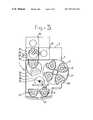
- FIGS. 2 and 3show the single device according to the present invention which combines the above devices and considerably simplifies the complicated operations while allowing more efficient handling of the wafers on a much smaller surface area.
- a sorting/storage deviceis denoted by 1 .
- This deviceis arranged in a housing 2 .
- This housing 2is preferably itself placed in a chamber which is not shown, such as a clean room.
- the housingis provided with a partition 4 .
- Partition 4provides a separation between chamber 23 and chamber 22 .
- a cassette-handling device 25such as a robot, and a magazine 8 for cassettes are situated in chamber 23 .
- Communication with chamber 22is realized via closable opening 37 which is designed in such a manner that, when cassette 18 is placed against it, both this cassette and the said opening 37 are opened. Consequently, it is possible for the wafer-handling device or wafer robot 24 arranged in chamber 22 to collect wafers from the cassette in question or to position them therein.
- This wafer-handling robot 24is able to move both in the horizontal plane and in the vertical plane and is controlled by control unit 20 .
- Any desired gas atmospherecan be maintained within a chamber 22 , for example a pure nitrogen atmosphere, in order to avoid any action on the wafers, and the number of particles can be reduced still further.
- measuring stationsare situated adjacent to chamber 22 .
- Each measuring stationis able to determine one or more different parameters, such as the layer thickness of material which has been deposited on the wafer, the chemical and/or physical state of this material, the number of dust particles on the wafer and the like.
- measuring stationsmay be placed in active connection with the wafer-handling robot at a number of positions.
- FIG. 2it can be seen from FIG. 2 that if the height of the measuring stations is limited, two or more measuring stations can be placed above one another within the reach of the wafer-handling robot.
- cassettes 18are arranged on a turntable 30 .
- cassette-handling device 25Using cassette-handling device 25 , cassettes can be moved from this turntable 30 to store 8 .
- This cassette-handling robot 25comprises a jointed arm 31 and a height-adjustment mechanism 35 .
- Store 8comprises a rotatable, cylindrical magazine provided with receptacles 26 , at different levels 27 , which receive cassettes 17 .
- Cassettes 12 , 13 , 17 and 18are, of course, identical.
- Store 8is of rotatable design. As a result, and because the cassette robot 25 is vertically adjustable, any cassette can be moved from the store onto the turntable 30 which is designed with two recesses. It will be understood that table 30 may have a greater number of levels.
- the cassettes 12 and 13are moved into the insertion/removal position 33 .
- the cassettes 12 and 13are moved into the insertion/removal position 33 .
- chamber 23When using so-called FOUPs, i.e. cassettes which normally close off their contents and are opened only on contact with partition 4 , chamber 23 may have the same atmosphere as the surroundings, for example clean-room conditions, and does not have to satisfy the higher demands imposed when sorting the wafers for particle concentration and the like.
- FOUPsi.e. cassettes which normally close off their contents and are opened only on contact with partition 4
- chamber 23may have the same atmosphere as the surroundings, for example clean-room conditions, and does not have to satisfy the higher demands imposed when sorting the wafers for particle concentration and the like.
- cassette 13which is empty is to be provided with a specific sequence of different types of wafers for treatment in, for example, a furnace, it is placed on turntable 30 using cassette-handling robot 25 . Following rotation of turntable 30 , cassette 13 is situated in the position of cassette 18 . It is then opened. Before this, after this or simultaneously, it is ensured that a cassette containing at least one desired wafer is situated at a different level of turntable 30 .
- the top part of turntable 30can move independently from bottom part of turntable 30 .
- Rotation of turntable 30like the movement of the sorting device 24 , store 8 and cassette-handling device 25 , is controlled by control unit 20 .
- cassette 18With the aid of wafer-handling device 24 . If other wafers are required and are not present in the stock cassette used, this stock cassette is exchanged for another which may come from store 8 . In this way, a desired batch is assembled in cassette 18 and is removed again using cassette-handling device 25 .
- the cassette in questioncan be placed back on turntable 30 via handling device 25 and a wafer can be fed to either the top or the bottom measuring station 16 with the aid of wafer-handling device 24 .
- a measuring stationthere may also be a station for reading the wafer identification code and one for the wafer orientation.
- Various types of measurements on various types of test wafers or various types of measurements on the same test waferare possible.
- the present inventionconsiderably limits the logistics of the test wafers, since they no longer have to move along the various measuring stations and the storage/sorting device is multifunctional.
Landscapes
- Engineering & Computer Science (AREA)
- Physics & Mathematics (AREA)
- Condensed Matter Physics & Semiconductors (AREA)
- General Physics & Mathematics (AREA)
- Manufacturing & Machinery (AREA)
- Computer Hardware Design (AREA)
- Microelectronics & Electronic Packaging (AREA)
- Power Engineering (AREA)
- Container, Conveyance, Adherence, Positioning, Of Wafer (AREA)
Abstract
Description
1. Field of the Invention
The present invention relates to a device for sorting wafers.
2. Description of the Related Art
Such a sort device is generally known in the prior art. If wafers are being treated batchwise, it is customary to include test wafers in a batch as well as end wafers wherein because they are used as “fill” in the batch, the quality of treatment of these wafers is lower due to the position in the treatment device, and these wafers cannot be used further, or can only be used further after they have been treated. If a batch of wafers comprises, for example, 100 wafers, they are fed in a number of cassettes to the appropriate treatment device, such as a furnace. Normally, such cassettes contain approximately twenty-five wafers, so that in such a case approximately four wafer cassettes are fed to the furnace. A number of these cassettes are filled only with “product” wafers. Moreover, a number of cassettes contain test wafers and the end wafers described above.
In addition to the sorting device, there are normally a separate storage device for cassettes and one or more separate measuring stations for carrying out measurements. This means that in the prior art three or more separate housings are present, each separately provided with a (wafer- or cassette-)handling device and a particle-free environment.
The wafers are handled in the sorting device and in the measuring stations in a particularly particle-free environment. Higher demands are placed on this environment than on a clean room in which wafers are transported in closed pods. From the moment at which the transport pod is opened and the cassette containing wafers is removed therefrom until the moment at which the cassette containing wafers is placed back in the transport pod and the transport pod is closed, this particularly particle-free environment has to be maintained. By providing the pod around the wafer cassette with a standardized door (SMIF, FOUP) and placing the cassette with this door against a wall of the sorting device with a closable opening and simultaneously opening cassette door and wall opening, it is possible to achieve a highly effective separation between clean room and wafer-sorting chamber. As a result, the demands which are imposed on the clean room can be of a low level, with a corresponding saving in the costs, while in the limited volume of the sorting device itself it is possible to maintain an environment which satisfies the most stringent of materials requirements. It is also possible to provide the environment of the sorting device with an inert gas, such as nitrogen. The same applies to the measuring station. There too, the wafers are handled in a particularly particle-free environment. Each sorting station and each measuring station must be provided with a lock mechanism. The storage of wafers in the closed cassettes can take place under less stringent clean-room conditions.
U.S. Pat. No. 4,776,744, from which the preamble ofclaim 1 is known, discloses a device for sorting wafers. A turn-table is present, having several blades on which an indexer is provided for holding and moving two cassettes. The blades can be moved below a wafer gripper for removal and introduction of wafers out and in the cassettes.
The object of the present invention is to provide a sorting/storage/measuring device which is easier and less expensive to produce and in which the surface area required for the device can be limited without, reducing the throughout capacity. In addition, the flexibility is to be enhanced. In one embodiment, the device for sorting wafers stored in cassettes includes, among others, a housing, a wafer handling device arranged in a chamber to be sealed off with respect to the housing, a part for receiving cassettes arranged in the housing and separated from the chamber by a partition, a store for closable cassettes arranged in the housing, and a handling device for closable cassettes arranged in the housing.
As a result, the sorting options are considerably increased, due to the fact that all the cassettes in the storage device are available to the sorting device. In addition, the necessary measurements can also be carried out during sorting without the need for transportation to a separate measuring station. Consequently, the number of handling operations decreases and the capacity of the device can be increased while reducing the surface area required. If the wafers are supplied and stored in cassettes in pods provided with a standard door (SMIF, FOUP), fewer lock mechanisms are required than with the three or more separate housings according to the prior art. If certain types of wafer are always present in a specific cassette, it is possible, by changing cassettes of this nature into a different cassette which is present in the sorting device, to assemble a batch as desired. Naturally, it is also possible to arrange different types of wafers in a storage cassette, so that exchange in the sorting device is less frequent.
It is possible for the sorting device to deal with more than two cassettes at a time.
According to an advantageous embodiment of the invention, the chamber in which the sorting is carried out comprises a measuring station or a measuring station is arranged in functional relationship with the wafer handling device. Preferably this measuring station is provided in the space wherein sorting is realised or a measuring station is provided adjacent thereto. Such a measuring station may, for example, be designed to test layer thickness of the treated wafers, to measure amount of undesirable foreign particles which are present on/in the wafers and the like.
The cassette-handling device is able to move the cassettes from the insertion position to the store or to a turntable. The turntable moves the cassette into the correct position for the lock mechanism via which the cassette is placed in active connection with the wafer-handling robot.
The store for cassettes may comprise any structure which is known in the prior art, such as a rotatable magazine.
The invention also relates to a method for assembling a (part of a) batch of wafers which is to be fed to a treatment device for wafers, comprising placing at least two cassettes containing wafers in active connection with a wafer-handling device and using the said wafer-handling device to carry out a sorting operation by moving wafers from one cassette to the other and vice versa. According to the invention, this method is characterized in that at least one of the said cassettes is from a cassette store, the said cassettes being moved from the said store to the sorting station in a housing.
According to an advantageous embodiment of this method, the wafer is subjected to a measurement during the sorting operation. “During” is also understood to encompass immediately before or immediately after the sorting operation.
The invention will be explained in more detail below with reference to a structure according to the prior art and an exemplary embodiment according to the invention. In the drawing:
InFIG. 1 a,40 denotes a sorting device which comprises a part (depicted highly diagrammatically) in which thecassettes circle 41. Using this device, wafers, for example, are removed fromcassette 12 and placed incassette 13 in any desired order.
To carry out a treatment in, for example, a furnace, such as a deposition process on a wafer, firstly, if required, measurements are carried out on test wafers in one ormore measuring stations 44, for example the number of dust particles present before the treatment is measured. Then, a batch is assembled indevice 40.Cassettes 12 containing different wafers which are required for his purpose come fromstore 42. After the appropriate treatment has been carried out, the wafers are sorted again instation 40 and are stored instation 42. The test wafers are measured in one or more measuringstations 44.
Transport between the various stations takes place in thecassettes
In theseFIGS. 2 ,3, a sorting/storage device according to the present invention is denoted by1. This device is arranged in ahousing 2. Thishousing 2 is preferably itself placed in a chamber which is not shown, such as a clean room.
As can be seen fromFIGS. 2 and 3 , the housing is provided with a partition4. Partition4 provides a separation betweenchamber 23 andchamber 22. A cassette-handlingdevice 25 such as a robot, and amagazine 8 for cassettes are situated inchamber 23. Communication withchamber 22 is realized via closable opening37 which is designed in such a manner that, whencassette 18 is placed against it, both this cassette and the said opening37 are opened. Consequently, it is possible for the wafer-handling device orwafer robot 24 arranged inchamber 22 to collect wafers from the cassette in question or to position them therein. This wafer-handlingrobot 24 is able to move both in the horizontal plane and in the vertical plane and is controlled by control unit20. Any desired gas atmosphere can be maintained within achamber 22, for example a pure nitrogen atmosphere, in order to avoid any action on the wafers, and the number of particles can be reduced still further.
Moreover, one or more measuring stations are situated adjacent tochamber 22. Each measuring station is able to determine one or more different parameters, such as the layer thickness of material which has been deposited on the wafer, the chemical and/or physical state of this material, the number of dust particles on the wafer and the like. As can be seen fromFIG. 3 , measuring stations may be placed in active connection with the wafer-handling robot at a number of positions. Moreover, it can be seen fromFIG. 2 that if the height of the measuring stations is limited, two or more measuring stations can be placed above one another within the reach of the wafer-handling robot.
Thesecassettes 18 are arranged on aturntable 30. Using cassette-handlingdevice 25, cassettes can be moved from thisturntable 30 tostore 8. This cassette-handlingrobot 25 comprises a jointedarm 31 and a height-adjustment mechanism 35.Store 8 comprises a rotatable, cylindrical magazine provided withreceptacles 26, atdifferent levels 27, which receivecassettes 17.Cassettes Store 8 is of rotatable design. As a result, and because thecassette robot 25 is vertically adjustable, any cassette can be moved from the store onto theturntable 30 which is designed with two recesses. It will be understood that table30 may have a greater number of levels.
On entry, thecassettes removal position 33. As diagrammatically indicated inFIG. 3 , it is possible, from this position, for example to placecassette 13 instore 8 or to transfer it directly toturntable 30.
When using so-called FOUPs, i.e. cassettes which normally close off their contents and are opened only on contact with partition4,chamber 23 may have the same atmosphere as the surroundings, for example clean-room conditions, and does not have to satisfy the higher demands imposed when sorting the wafers for particle concentration and the like.
The device described above functions as follows. If, for example,cassette 13 which is empty is to be provided with a specific sequence of different types of wafers for treatment in, for example, a furnace, it is placed onturntable 30 using cassette-handlingrobot 25. Following rotation ofturntable 30,cassette 13 is situated in the position ofcassette 18. It is then opened. Before this, after this or simultaneously, it is ensured that a cassette containing at least one desired wafer is situated at a different level ofturntable 30. For this purpose, the top part ofturntable 30 can move independently from bottom part ofturntable 30. Rotation ofturntable 30, like the movement of thesorting device 24,store 8 and cassette-handlingdevice 25, is controlled by control unit20. Then, the desired wafer is placed incassette 18 with the aid of wafer-handlingdevice 24. If other wafers are required and are not present in the stock cassette used, this stock cassette is exchanged for another which may come fromstore 8. In this way, a desired batch is assembled incassette 18 and is removed again using cassette-handlingdevice 25.
After the treatment has finished, the cassette in question can be placed back onturntable 30 via handlingdevice 25 and a wafer can be fed to either the top or thebottom measuring station 16 with the aid of wafer-handlingdevice 24. In addition to a measuring station, there may also be a station for reading the wafer identification code and one for the wafer orientation. Various types of measurements on various types of test wafers or various types of measurements on the same test wafer are possible.
The present invention considerably limits the logistics of the test wafers, since they no longer have to move along the various measuring stations and the storage/sorting device is multifunctional. In addition to advantages in the area of the housing and the atmosphere present therein, it is also possible to simplify automation, since the number of wafer-/cassette-handling robots can be limited, as can their expensive control unit20.
Although the invention is described above with reference to a preferred embodiment, it will be understood that numerous amendments can be made to this without departing from the scope of the present claims. For example, it is possible for the storage device to be designed in any other way which is known from the prior art. Moreover, there may be devices for determining the position of the wafer on the wafer-handling robot.
Claims (5)
1. A device for sorting wafers stored in cassettes comprising:
a housing;
a wafer handling device arranged in a chamber configured to be sealed off with respect to the housing, wherein the wafer-handling device accesses a measuring station configured to carry out measurements directly on said wafers;
a part for receiving at least two closable cassettes arranged in the housing and separated from said chamber by a partition, said part configured to independently position each received cassette against a related closable opening in said partition, wherein through opening of said closable opening said closable cassette is opened when placed against the opening and placed in communication with said chamber so that said wafer handling device can sort wafers by moving the wafers into and out from one cassette and into an other cassette after opening each of said at least two cassettes;
a store for closable cassettes arranged in the housing; and
a handling device for closable cassettes arranged in the housing, wherein the store for closable cassettes and the handling device for closable cassettes are separated from the part for receiving at least two cassettes, wherein the part for receiving at least two cassettes comprises a turntable, wherein said turntable comprises two or more levels which are independently rotatable, wherein the turntable is configured to receive one of the at least two cassettes on each of the two or more levels, wherein said turntable is configured to place each of the at least two cassettes in a position against a related closeable opening.
2. The device ofclaim 1 , wherein the device is configured for sorting wafers stored in FOUPs.
3. The device ofclaim 1 , wherein the store for cassettes comprises a rotatable magazine.
4. A method for assembling a batch of wafers in cassettes comprising the steps of:
placing at least a first and a second closed cassette in a store;
employing a cassette handling device to select and move a first cassette from the store to a first closable opening in a sealed chamber;
opening said first closable opening together with said first cassette;
employing a cassette handling device to select and move a second cassette from the store to a second closable opening in said sealed chamber;
opening said second closable opening together with said second cassette;
performing a direct measurement of said wafers in a measuring station; and
employing a wafer-handling device, provided in said sealed chamber, to transfer wafers to and from the measuring station communicating with said sealed chamber and to sort the wafers by transferring wafers directly between the first cassette and the second cassette,
wherein employing the cassette handling device to select and move the first cassette comprises:
moving the first cassette from the store to a recess on a first level of a turntable; and
rotating the first level of the turntable so as to move the first cassette to the first closable opening; and
wherein employing the cassette handling device to select and move the second cassette comprises:
moving the second cassette from the store to a recess on a second level of the turntable; and
rotating the second level of the turntable independently of the first level so as to move the second cassette to the second closable opening.
5. The method ofclaim 4 , further comprising the step of testing the wafers during sorting the wafers.
Applications Claiming Priority (2)
| Application Number | Priority Date | Filing Date | Title |
|---|---|---|---|
| NL1010317ANL1010317C2 (en) | 1998-10-14 | 1998-10-14 | Sorting / storage device for wafers and method for handling them. |
| PCT/NL1999/000583WO2000022653A1 (en) | 1998-10-14 | 1999-09-21 | Sorting/storage device for wafers and method for handling thereof |
Publications (1)
| Publication Number | Publication Date |
|---|---|
| US7077614B1true US7077614B1 (en) | 2006-07-18 |
Family
ID=19767964
Family Applications (1)
| Application Number | Title | Priority Date | Filing Date |
|---|---|---|---|
| US09/807,580Expired - LifetimeUS7077614B1 (en) | 1998-10-14 | 1999-09-21 | Sorting/storage device for wafers and method for handling thereof |
Country Status (8)
| Country | Link |
|---|---|
| US (1) | US7077614B1 (en) |
| EP (1) | EP1121712B1 (en) |
| JP (1) | JP2002527901A (en) |
| KR (1) | KR20010075625A (en) |
| DE (1) | DE69924131T2 (en) |
| NL (1) | NL1010317C2 (en) |
| TW (1) | TW424292B (en) |
| WO (1) | WO2000022653A1 (en) |
Cited By (315)
| Publication number | Priority date | Publication date | Assignee | Title |
|---|---|---|---|---|
| US20080069672A1 (en)* | 2006-09-13 | 2008-03-20 | Daifuku Co., Ltd. | Substrate storage facility and substrate processing facility, and method for operating substrate storage |
| US20080089765A1 (en)* | 2006-09-13 | 2008-04-17 | Daifuku Co., Ltd. | Method for processing substrates |
| US20080260502A1 (en)* | 2007-04-02 | 2008-10-23 | Hitachi Kokusai Electric Inc. | Substrate processing apparatus and semiconductor device manufacturing method |
| US20080286076A1 (en)* | 2004-07-14 | 2008-11-20 | Applied Materials, Inc. | Methods and apparatus for repositioning support for a substrate carrier |
| US20090087287A1 (en)* | 2007-09-28 | 2009-04-02 | Taiwan Semiconductor Manufacturing Co., Ltd. | Apparatus and method for semiconductor wafer transfer |
| US20090261047A1 (en)* | 2008-04-17 | 2009-10-22 | Teradyne, Inc. | Enclosed Operating Area For Disk Drive Testing Systems |
| US20090262455A1 (en)* | 2008-04-17 | 2009-10-22 | Teradyne, Inc. | Temperature Control Within Disk Drive Testing Systems |
| US7778031B1 (en) | 2009-07-15 | 2010-08-17 | Teradyne, Inc. | Test slot cooling system for a storage device testing system |
| US7848106B2 (en) | 2008-04-17 | 2010-12-07 | Teradyne, Inc. | Temperature control within disk drive testing systems |
| US7890207B2 (en) | 2008-04-17 | 2011-02-15 | Teradyne, Inc. | Transferring storage devices within storage device testing systems |
| US7904211B2 (en) | 2008-04-17 | 2011-03-08 | Teradyne, Inc. | Dependent temperature control within disk drive testing systems |
| US7908029B2 (en) | 2008-06-03 | 2011-03-15 | Teradyne, Inc. | Processing storage devices |
| US7911778B2 (en) | 2008-04-17 | 2011-03-22 | Teradyne, Inc. | Vibration isolation within disk drive testing systems |
| US7929303B1 (en) | 2010-02-02 | 2011-04-19 | Teradyne, Inc. | Storage device testing system cooling |
| US7932734B2 (en) | 2009-07-15 | 2011-04-26 | Teradyne, Inc. | Individually heating storage devices in a testing system |
| US7940529B2 (en) | 2009-07-15 | 2011-05-10 | Teradyne, Inc. | Storage device temperature sensing |
| US7945424B2 (en) | 2008-04-17 | 2011-05-17 | Teradyne, Inc. | Disk drive emulator and method of use thereof |
| US7987018B2 (en) | 2008-04-17 | 2011-07-26 | Teradyne, Inc. | Transferring disk drives within disk drive testing systems |
| US7996174B2 (en) | 2007-12-18 | 2011-08-09 | Teradyne, Inc. | Disk drive testing |
| US8041449B2 (en) | 2008-04-17 | 2011-10-18 | Teradyne, Inc. | Bulk feeding disk drives to disk drive testing systems |
| US8102173B2 (en) | 2008-04-17 | 2012-01-24 | Teradyne, Inc. | Thermal control system for test slot of test rack for disk drive testing system with thermoelectric device and a cooling conduit |
| US8116079B2 (en) | 2009-07-15 | 2012-02-14 | Teradyne, Inc. | Storage device testing system cooling |
| US8405971B2 (en) | 2007-12-18 | 2013-03-26 | Teradyne, Inc. | Disk drive transport, clamping and testing |
| US20130123966A1 (en)* | 2011-11-14 | 2013-05-16 | Shenzhen China Star Optoelectronics Technology Co., Ltd. | Spatial three-dimensional inline handling system |
| US8547123B2 (en) | 2009-07-15 | 2013-10-01 | Teradyne, Inc. | Storage device testing system with a conductive heating assembly |
| US8628239B2 (en) | 2009-07-15 | 2014-01-14 | Teradyne, Inc. | Storage device temperature sensing |
| US8687349B2 (en) | 2010-07-21 | 2014-04-01 | Teradyne, Inc. | Bulk transfer of storage devices using manual loading |
| US9001456B2 (en) | 2010-08-31 | 2015-04-07 | Teradyne, Inc. | Engaging test slots |
| US9459312B2 (en) | 2013-04-10 | 2016-10-04 | Teradyne, Inc. | Electronic assembly test system |
| US9779780B2 (en) | 2010-06-17 | 2017-10-03 | Teradyne, Inc. | Damping vibrations within storage device testing systems |
| US10725091B2 (en) | 2017-08-28 | 2020-07-28 | Teradyne, Inc. | Automated test system having multiple stages |
| US10775408B2 (en) | 2018-08-20 | 2020-09-15 | Teradyne, Inc. | System for testing devices inside of carriers |
| US10845410B2 (en) | 2017-08-28 | 2020-11-24 | Teradyne, Inc. | Automated test system having orthogonal robots |
| US10948534B2 (en) | 2017-08-28 | 2021-03-16 | Teradyne, Inc. | Automated test system employing robotics |
| US10983145B2 (en) | 2018-04-24 | 2021-04-20 | Teradyne, Inc. | System for testing devices inside of carriers |
| US11001925B2 (en) | 2016-12-19 | 2021-05-11 | Asm Ip Holding B.V. | Substrate processing apparatus |
| US11004977B2 (en) | 2017-07-19 | 2021-05-11 | Asm Ip Holding B.V. | Method for depositing a group IV semiconductor and related semiconductor device structures |
| US11015245B2 (en) | 2014-03-19 | 2021-05-25 | Asm Ip Holding B.V. | Gas-phase reactor and system having exhaust plenum and components thereof |
| US11018002B2 (en) | 2017-07-19 | 2021-05-25 | Asm Ip Holding B.V. | Method for selectively depositing a Group IV semiconductor and related semiconductor device structures |
| US11022879B2 (en) | 2017-11-24 | 2021-06-01 | Asm Ip Holding B.V. | Method of forming an enhanced unexposed photoresist layer |
| US11031242B2 (en) | 2018-11-07 | 2021-06-08 | Asm Ip Holding B.V. | Methods for depositing a boron doped silicon germanium film |
| USD922229S1 (en) | 2019-06-05 | 2021-06-15 | Asm Ip Holding B.V. | Device for controlling a temperature of a gas supply unit |
| US11049751B2 (en) | 2018-09-14 | 2021-06-29 | Asm Ip Holding B.V. | Cassette supply system to store and handle cassettes and processing apparatus equipped therewith |
| US11056344B2 (en) | 2017-08-30 | 2021-07-06 | Asm Ip Holding B.V. | Layer forming method |
| US11053591B2 (en) | 2018-08-06 | 2021-07-06 | Asm Ip Holding B.V. | Multi-port gas injection system and reactor system including same |
| US11069510B2 (en) | 2017-08-30 | 2021-07-20 | Asm Ip Holding B.V. | Substrate processing apparatus |
| US11081345B2 (en) | 2018-02-06 | 2021-08-03 | Asm Ip Holding B.V. | Method of post-deposition treatment for silicon oxide film |
| US11088002B2 (en) | 2018-03-29 | 2021-08-10 | Asm Ip Holding B.V. | Substrate rack and a substrate processing system and method |
| US11087997B2 (en) | 2018-10-31 | 2021-08-10 | Asm Ip Holding B.V. | Substrate processing apparatus for processing substrates |
| US11094582B2 (en) | 2016-07-08 | 2021-08-17 | Asm Ip Holding B.V. | Selective deposition method to form air gaps |
| US11094546B2 (en) | 2017-10-05 | 2021-08-17 | Asm Ip Holding B.V. | Method for selectively depositing a metallic film on a substrate |
| US11101370B2 (en) | 2016-05-02 | 2021-08-24 | Asm Ip Holding B.V. | Method of forming a germanium oxynitride film |
| US11107676B2 (en) | 2016-07-28 | 2021-08-31 | Asm Ip Holding B.V. | Method and apparatus for filling a gap |
| US11114283B2 (en) | 2018-03-16 | 2021-09-07 | Asm Ip Holding B.V. | Reactor, system including the reactor, and methods of manufacturing and using same |
| US11114294B2 (en) | 2019-03-08 | 2021-09-07 | Asm Ip Holding B.V. | Structure including SiOC layer and method of forming same |
| USD930782S1 (en) | 2019-08-22 | 2021-09-14 | Asm Ip Holding B.V. | Gas distributor |
| US11127617B2 (en) | 2017-11-27 | 2021-09-21 | Asm Ip Holding B.V. | Storage device for storing wafer cassettes for use with a batch furnace |
| US11127589B2 (en) | 2019-02-01 | 2021-09-21 | Asm Ip Holding B.V. | Method of topology-selective film formation of silicon oxide |
| USD931978S1 (en) | 2019-06-27 | 2021-09-28 | Asm Ip Holding B.V. | Showerhead vacuum transport |
| US11139191B2 (en) | 2017-08-09 | 2021-10-05 | Asm Ip Holding B.V. | Storage apparatus for storing cassettes for substrates and processing apparatus equipped therewith |
| US11139308B2 (en) | 2015-12-29 | 2021-10-05 | Asm Ip Holding B.V. | Atomic layer deposition of III-V compounds to form V-NAND devices |
| US11158513B2 (en) | 2018-12-13 | 2021-10-26 | Asm Ip Holding B.V. | Methods for forming a rhenium-containing film on a substrate by a cyclical deposition process and related semiconductor device structures |
| US11164955B2 (en) | 2017-07-18 | 2021-11-02 | Asm Ip Holding B.V. | Methods for forming a semiconductor device structure and related semiconductor device structures |
| US11168395B2 (en) | 2018-06-29 | 2021-11-09 | Asm Ip Holding B.V. | Temperature-controlled flange and reactor system including same |
| USD935572S1 (en) | 2019-05-24 | 2021-11-09 | Asm Ip Holding B.V. | Gas channel plate |
| US11171025B2 (en) | 2019-01-22 | 2021-11-09 | Asm Ip Holding B.V. | Substrate processing device |
| US11205585B2 (en) | 2016-07-28 | 2021-12-21 | Asm Ip Holding B.V. | Substrate processing apparatus and method of operating the same |
| US11217444B2 (en) | 2018-11-30 | 2022-01-04 | Asm Ip Holding B.V. | Method for forming an ultraviolet radiation responsive metal oxide-containing film |
| US11222772B2 (en) | 2016-12-14 | 2022-01-11 | Asm Ip Holding B.V. | Substrate processing apparatus |
| USD940837S1 (en) | 2019-08-22 | 2022-01-11 | Asm Ip Holding B.V. | Electrode |
| US11227789B2 (en) | 2019-02-20 | 2022-01-18 | Asm Ip Holding B.V. | Method and apparatus for filling a recess formed within a substrate surface |
| US11227782B2 (en) | 2019-07-31 | 2022-01-18 | Asm Ip Holding B.V. | Vertical batch furnace assembly |
| US11226390B2 (en) | 2017-08-28 | 2022-01-18 | Teradyne, Inc. | Calibration process for an automated test system |
| US11230766B2 (en) | 2018-03-29 | 2022-01-25 | Asm Ip Holding B.V. | Substrate processing apparatus and method |
| US11233133B2 (en) | 2015-10-21 | 2022-01-25 | Asm Ip Holding B.V. | NbMC layers |
| US11232963B2 (en) | 2018-10-03 | 2022-01-25 | Asm Ip Holding B.V. | Substrate processing apparatus and method |
| US11244825B2 (en) | 2018-11-16 | 2022-02-08 | Asm Ip Holding B.V. | Methods for depositing a transition metal chalcogenide film on a substrate by a cyclical deposition process |
| US11242598B2 (en) | 2015-06-26 | 2022-02-08 | Asm Ip Holding B.V. | Structures including metal carbide material, devices including the structures, and methods of forming same |
| US11251040B2 (en) | 2019-02-20 | 2022-02-15 | Asm Ip Holding B.V. | Cyclical deposition method including treatment step and apparatus for same |
| US11251068B2 (en) | 2018-10-19 | 2022-02-15 | Asm Ip Holding B.V. | Substrate processing apparatus and substrate processing method |
| US11251035B2 (en) | 2016-12-22 | 2022-02-15 | Asm Ip Holding B.V. | Method of forming a structure on a substrate |
| USD944946S1 (en) | 2019-06-14 | 2022-03-01 | Asm Ip Holding B.V. | Shower plate |
| US11270899B2 (en) | 2018-06-04 | 2022-03-08 | Asm Ip Holding B.V. | Wafer handling chamber with moisture reduction |
| US11274369B2 (en) | 2018-09-11 | 2022-03-15 | Asm Ip Holding B.V. | Thin film deposition method |
| US11282698B2 (en) | 2019-07-19 | 2022-03-22 | Asm Ip Holding B.V. | Method of forming topology-controlled amorphous carbon polymer film |
| US11289326B2 (en) | 2019-05-07 | 2022-03-29 | Asm Ip Holding B.V. | Method for reforming amorphous carbon polymer film |
| US11286562B2 (en) | 2018-06-08 | 2022-03-29 | Asm Ip Holding B.V. | Gas-phase chemical reactor and method of using same |
| US11286558B2 (en) | 2019-08-23 | 2022-03-29 | Asm Ip Holding B.V. | Methods for depositing a molybdenum nitride film on a surface of a substrate by a cyclical deposition process and related semiconductor device structures including a molybdenum nitride film |
| US11296189B2 (en) | 2018-06-21 | 2022-04-05 | Asm Ip Holding B.V. | Method for depositing a phosphorus doped silicon arsenide film and related semiconductor device structures |
| US11295980B2 (en) | 2017-08-30 | 2022-04-05 | Asm Ip Holding B.V. | Methods for depositing a molybdenum metal film over a dielectric surface of a substrate by a cyclical deposition process and related semiconductor device structures |
| USD947913S1 (en) | 2019-05-17 | 2022-04-05 | Asm Ip Holding B.V. | Susceptor shaft |
| USD948463S1 (en) | 2018-10-24 | 2022-04-12 | Asm Ip Holding B.V. | Susceptor for semiconductor substrate supporting apparatus |
| USD949319S1 (en) | 2019-08-22 | 2022-04-19 | Asm Ip Holding B.V. | Exhaust duct |
| US11306395B2 (en) | 2017-06-28 | 2022-04-19 | Asm Ip Holding B.V. | Methods for depositing a transition metal nitride film on a substrate by atomic layer deposition and related deposition apparatus |
| US11315794B2 (en) | 2019-10-21 | 2022-04-26 | Asm Ip Holding B.V. | Apparatus and methods for selectively etching films |
| US11342216B2 (en) | 2019-02-20 | 2022-05-24 | Asm Ip Holding B.V. | Cyclical deposition method and apparatus for filling a recess formed within a substrate surface |
| US11339476B2 (en) | 2019-10-08 | 2022-05-24 | Asm Ip Holding B.V. | Substrate processing device having connection plates, substrate processing method |
| US11345999B2 (en) | 2019-06-06 | 2022-05-31 | Asm Ip Holding B.V. | Method of using a gas-phase reactor system including analyzing exhausted gas |
| US11355338B2 (en) | 2019-05-10 | 2022-06-07 | Asm Ip Holding B.V. | Method of depositing material onto a surface and structure formed according to the method |
| US11361990B2 (en) | 2018-05-28 | 2022-06-14 | Asm Ip Holding B.V. | Substrate processing method and device manufactured by using the same |
| US11374112B2 (en) | 2017-07-19 | 2022-06-28 | Asm Ip Holding B.V. | Method for depositing a group IV semiconductor and related semiconductor device structures |
| US11378337B2 (en) | 2019-03-28 | 2022-07-05 | Asm Ip Holding B.V. | Door opener and substrate processing apparatus provided therewith |
| US11387120B2 (en) | 2017-09-28 | 2022-07-12 | Asm Ip Holding B.V. | Chemical dispensing apparatus and methods for dispensing a chemical to a reaction chamber |
| US11387106B2 (en) | 2018-02-14 | 2022-07-12 | Asm Ip Holding B.V. | Method for depositing a ruthenium-containing film on a substrate by a cyclical deposition process |
| US11390946B2 (en) | 2019-01-17 | 2022-07-19 | Asm Ip Holding B.V. | Methods of forming a transition metal containing film on a substrate by a cyclical deposition process |
| US11393690B2 (en) | 2018-01-19 | 2022-07-19 | Asm Ip Holding B.V. | Deposition method |
| US11390945B2 (en) | 2019-07-03 | 2022-07-19 | Asm Ip Holding B.V. | Temperature control assembly for substrate processing apparatus and method of using same |
| US11390950B2 (en) | 2017-01-10 | 2022-07-19 | Asm Ip Holding B.V. | Reactor system and method to reduce residue buildup during a film deposition process |
| US11398382B2 (en) | 2018-03-27 | 2022-07-26 | Asm Ip Holding B.V. | Method of forming an electrode on a substrate and a semiconductor device structure including an electrode |
| US11396702B2 (en) | 2016-11-15 | 2022-07-26 | Asm Ip Holding B.V. | Gas supply unit and substrate processing apparatus including the gas supply unit |
| US11401605B2 (en) | 2019-11-26 | 2022-08-02 | Asm Ip Holding B.V. | Substrate processing apparatus |
| US11411088B2 (en) | 2018-11-16 | 2022-08-09 | Asm Ip Holding B.V. | Methods for forming a metal silicate film on a substrate in a reaction chamber and related semiconductor device structures |
| US11410851B2 (en) | 2017-02-15 | 2022-08-09 | Asm Ip Holding B.V. | Methods for forming a metallic film on a substrate by cyclical deposition and related semiconductor device structures |
| US11414760B2 (en) | 2018-10-08 | 2022-08-16 | Asm Ip Holding B.V. | Substrate support unit, thin film deposition apparatus including the same, and substrate processing apparatus including the same |
| US11417545B2 (en) | 2017-08-08 | 2022-08-16 | Asm Ip Holding B.V. | Radiation shield |
| US11424119B2 (en) | 2019-03-08 | 2022-08-23 | Asm Ip Holding B.V. | Method for selective deposition of silicon nitride layer and structure including selectively-deposited silicon nitride layer |
| US11430674B2 (en) | 2018-08-22 | 2022-08-30 | Asm Ip Holding B.V. | Sensor array, apparatus for dispensing a vapor phase reactant to a reaction chamber and related methods |
| US11430640B2 (en) | 2019-07-30 | 2022-08-30 | Asm Ip Holding B.V. | Substrate processing apparatus |
| US11437241B2 (en) | 2020-04-08 | 2022-09-06 | Asm Ip Holding B.V. | Apparatus and methods for selectively etching silicon oxide films |
| US11443926B2 (en) | 2019-07-30 | 2022-09-13 | Asm Ip Holding B.V. | Substrate processing apparatus |
| US11447864B2 (en) | 2019-04-19 | 2022-09-20 | Asm Ip Holding B.V. | Layer forming method and apparatus |
| US11447861B2 (en) | 2016-12-15 | 2022-09-20 | Asm Ip Holding B.V. | Sequential infiltration synthesis apparatus and a method of forming a patterned structure |
| USD965044S1 (en) | 2019-08-19 | 2022-09-27 | Asm Ip Holding B.V. | Susceptor shaft |
| US11453943B2 (en) | 2016-05-25 | 2022-09-27 | Asm Ip Holding B.V. | Method for forming carbon-containing silicon/metal oxide or nitride film by ALD using silicon precursor and hydrocarbon precursor |
| USD965524S1 (en) | 2019-08-19 | 2022-10-04 | Asm Ip Holding B.V. | Susceptor support |
| US11469098B2 (en) | 2018-05-08 | 2022-10-11 | Asm Ip Holding B.V. | Methods for depositing an oxide film on a substrate by a cyclical deposition process and related device structures |
| US11476109B2 (en) | 2019-06-11 | 2022-10-18 | Asm Ip Holding B.V. | Method of forming an electronic structure using reforming gas, system for performing the method, and structure formed using the method |
| US11473195B2 (en) | 2018-03-01 | 2022-10-18 | Asm Ip Holding B.V. | Semiconductor processing apparatus and a method for processing a substrate |
| US11482533B2 (en) | 2019-02-20 | 2022-10-25 | Asm Ip Holding B.V. | Apparatus and methods for plug fill deposition in 3-D NAND applications |
| US11482418B2 (en) | 2018-02-20 | 2022-10-25 | Asm Ip Holding B.V. | Substrate processing method and apparatus |
| US11482412B2 (en) | 2018-01-19 | 2022-10-25 | Asm Ip Holding B.V. | Method for depositing a gap-fill layer by plasma-assisted deposition |
| US11488819B2 (en) | 2018-12-04 | 2022-11-01 | Asm Ip Holding B.V. | Method of cleaning substrate processing apparatus |
| US11488854B2 (en) | 2020-03-11 | 2022-11-01 | Asm Ip Holding B.V. | Substrate handling device with adjustable joints |
| US11495459B2 (en) | 2019-09-04 | 2022-11-08 | Asm Ip Holding B.V. | Methods for selective deposition using a sacrificial capping layer |
| US11492703B2 (en) | 2018-06-27 | 2022-11-08 | Asm Ip Holding B.V. | Cyclic deposition methods for forming metal-containing material and films and structures including the metal-containing material |
| US11499226B2 (en) | 2018-11-02 | 2022-11-15 | Asm Ip Holding B.V. | Substrate supporting unit and a substrate processing device including the same |
| US11501956B2 (en) | 2012-10-12 | 2022-11-15 | Asm Ip Holding B.V. | Semiconductor reaction chamber showerhead |
| US11501973B2 (en) | 2018-01-16 | 2022-11-15 | Asm Ip Holding B.V. | Method for depositing a material film on a substrate within a reaction chamber by a cyclical deposition process and related device structures |
| US11499222B2 (en) | 2018-06-27 | 2022-11-15 | Asm Ip Holding B.V. | Cyclic deposition methods for forming metal-containing material and films and structures including the metal-containing material |
| US11501968B2 (en) | 2019-11-15 | 2022-11-15 | Asm Ip Holding B.V. | Method for providing a semiconductor device with silicon filled gaps |
| US11515188B2 (en) | 2019-05-16 | 2022-11-29 | Asm Ip Holding B.V. | Wafer boat handling device, vertical batch furnace and method |
| US11515187B2 (en) | 2020-05-01 | 2022-11-29 | Asm Ip Holding B.V. | Fast FOUP swapping with a FOUP handler |
| US11521851B2 (en) | 2020-02-03 | 2022-12-06 | Asm Ip Holding B.V. | Method of forming structures including a vanadium or indium layer |
| US11527400B2 (en) | 2019-08-23 | 2022-12-13 | Asm Ip Holding B.V. | Method for depositing silicon oxide film having improved quality by peald using bis(diethylamino)silane |
| US11527403B2 (en) | 2019-12-19 | 2022-12-13 | Asm Ip Holding B.V. | Methods for filling a gap feature on a substrate surface and related semiconductor structures |
| US11532757B2 (en) | 2016-10-27 | 2022-12-20 | Asm Ip Holding B.V. | Deposition of charge trapping layers |
| US11530483B2 (en) | 2018-06-21 | 2022-12-20 | Asm Ip Holding B.V. | Substrate processing system |
| US11530876B2 (en) | 2020-04-24 | 2022-12-20 | Asm Ip Holding B.V. | Vertical batch furnace assembly comprising a cooling gas supply |
| US11551925B2 (en) | 2019-04-01 | 2023-01-10 | Asm Ip Holding B.V. | Method for manufacturing a semiconductor device |
| US11551912B2 (en) | 2020-01-20 | 2023-01-10 | Asm Ip Holding B.V. | Method of forming thin film and method of modifying surface of thin film |
| USD975665S1 (en) | 2019-05-17 | 2023-01-17 | Asm Ip Holding B.V. | Susceptor shaft |
| US11557474B2 (en) | 2019-07-29 | 2023-01-17 | Asm Ip Holding B.V. | Methods for selective deposition utilizing n-type dopants and/or alternative dopants to achieve high dopant incorporation |
| US11562901B2 (en) | 2019-09-25 | 2023-01-24 | Asm Ip Holding B.V. | Substrate processing method |
| US11572620B2 (en) | 2018-11-06 | 2023-02-07 | Asm Ip Holding B.V. | Methods for selectively depositing an amorphous silicon film on a substrate |
| US11581186B2 (en) | 2016-12-15 | 2023-02-14 | Asm Ip Holding B.V. | Sequential infiltration synthesis apparatus |
| US11587815B2 (en) | 2019-07-31 | 2023-02-21 | Asm Ip Holding B.V. | Vertical batch furnace assembly |
| US11587814B2 (en) | 2019-07-31 | 2023-02-21 | Asm Ip Holding B.V. | Vertical batch furnace assembly |
| US11587821B2 (en) | 2017-08-08 | 2023-02-21 | Asm Ip Holding B.V. | Substrate lift mechanism and reactor including same |
| US11594450B2 (en) | 2019-08-22 | 2023-02-28 | Asm Ip Holding B.V. | Method for forming a structure with a hole |
| USD979506S1 (en) | 2019-08-22 | 2023-02-28 | Asm Ip Holding B.V. | Insulator |
| US11594600B2 (en) | 2019-11-05 | 2023-02-28 | Asm Ip Holding B.V. | Structures with doped semiconductor layers and methods and systems for forming same |
| US11605528B2 (en) | 2019-07-09 | 2023-03-14 | Asm Ip Holding B.V. | Plasma device using coaxial waveguide, and substrate treatment method |
| USD980813S1 (en) | 2021-05-11 | 2023-03-14 | Asm Ip Holding B.V. | Gas flow control plate for substrate processing apparatus |
| USD980814S1 (en) | 2021-05-11 | 2023-03-14 | Asm Ip Holding B.V. | Gas distributor for substrate processing apparatus |
| US11610774B2 (en) | 2019-10-02 | 2023-03-21 | Asm Ip Holding B.V. | Methods for forming a topographically selective silicon oxide film by a cyclical plasma-enhanced deposition process |
| US11610775B2 (en) | 2016-07-28 | 2023-03-21 | Asm Ip Holding B.V. | Method and apparatus for filling a gap |
| US11615970B2 (en) | 2019-07-17 | 2023-03-28 | Asm Ip Holding B.V. | Radical assist ignition plasma system and method |
| USD981973S1 (en) | 2021-05-11 | 2023-03-28 | Asm Ip Holding B.V. | Reactor wall for substrate processing apparatus |
| US11626316B2 (en) | 2019-11-20 | 2023-04-11 | Asm Ip Holding B.V. | Method of depositing carbon-containing material on a surface of a substrate, structure formed using the method, and system for forming the structure |
| US11626308B2 (en) | 2020-05-13 | 2023-04-11 | Asm Ip Holding B.V. | Laser alignment fixture for a reactor system |
| US11629406B2 (en) | 2018-03-09 | 2023-04-18 | Asm Ip Holding B.V. | Semiconductor processing apparatus comprising one or more pyrometers for measuring a temperature of a substrate during transfer of the substrate |
| US11629407B2 (en) | 2019-02-22 | 2023-04-18 | Asm Ip Holding B.V. | Substrate processing apparatus and method for processing substrates |
| US11637014B2 (en) | 2019-10-17 | 2023-04-25 | Asm Ip Holding B.V. | Methods for selective deposition of doped semiconductor material |
| US11637011B2 (en) | 2019-10-16 | 2023-04-25 | Asm Ip Holding B.V. | Method of topology-selective film formation of silicon oxide |
| US11639811B2 (en) | 2017-11-27 | 2023-05-02 | Asm Ip Holding B.V. | Apparatus including a clean mini environment |
| US11639548B2 (en) | 2019-08-21 | 2023-05-02 | Asm Ip Holding B.V. | Film-forming material mixed-gas forming device and film forming device |
| US11646197B2 (en) | 2018-07-03 | 2023-05-09 | Asm Ip Holding B.V. | Method for depositing silicon-free carbon-containing film as gap-fill layer by pulse plasma-assisted deposition |
| US11643724B2 (en) | 2019-07-18 | 2023-05-09 | Asm Ip Holding B.V. | Method of forming structures using a neutral beam |
| US11646184B2 (en) | 2019-11-29 | 2023-05-09 | Asm Ip Holding B.V. | Substrate processing apparatus |
| US11646205B2 (en) | 2019-10-29 | 2023-05-09 | Asm Ip Holding B.V. | Methods of selectively forming n-type doped material on a surface, systems for selectively forming n-type doped material, and structures formed using same |
| US11644758B2 (en) | 2020-07-17 | 2023-05-09 | Asm Ip Holding B.V. | Structures and methods for use in photolithography |
| US11646204B2 (en) | 2020-06-24 | 2023-05-09 | Asm Ip Holding B.V. | Method for forming a layer provided with silicon |
| US11649546B2 (en) | 2016-07-08 | 2023-05-16 | Asm Ip Holding B.V. | Organic reactants for atomic layer deposition |
| US11658030B2 (en) | 2017-03-29 | 2023-05-23 | Asm Ip Holding B.V. | Method for forming doped metal oxide films on a substrate by cyclical deposition and related semiconductor device structures |
| US11658029B2 (en) | 2018-12-14 | 2023-05-23 | Asm Ip Holding B.V. | Method of forming a device structure using selective deposition of gallium nitride and system for same |
| US11658035B2 (en) | 2020-06-30 | 2023-05-23 | Asm Ip Holding B.V. | Substrate processing method |
| US11664245B2 (en) | 2019-07-16 | 2023-05-30 | Asm Ip Holding B.V. | Substrate processing device |
| US11664199B2 (en) | 2018-10-19 | 2023-05-30 | Asm Ip Holding B.V. | Substrate processing apparatus and substrate processing method |
| US11664267B2 (en) | 2019-07-10 | 2023-05-30 | Asm Ip Holding B.V. | Substrate support assembly and substrate processing device including the same |
| US11676812B2 (en) | 2016-02-19 | 2023-06-13 | Asm Ip Holding B.V. | Method for forming silicon nitride film selectively on top/bottom portions |
| US11674220B2 (en) | 2020-07-20 | 2023-06-13 | Asm Ip Holding B.V. | Method for depositing molybdenum layers using an underlayer |
| US11680839B2 (en) | 2019-08-05 | 2023-06-20 | Asm Ip Holding B.V. | Liquid level sensor for a chemical source vessel |
| US11685991B2 (en) | 2018-02-14 | 2023-06-27 | Asm Ip Holding B.V. | Method for depositing a ruthenium-containing film on a substrate by a cyclical deposition process |
| US11688603B2 (en) | 2019-07-17 | 2023-06-27 | Asm Ip Holding B.V. | Methods of forming silicon germanium structures |
| USD990441S1 (en) | 2021-09-07 | 2023-06-27 | Asm Ip Holding B.V. | Gas flow control plate |
| USD990534S1 (en) | 2020-09-11 | 2023-06-27 | Asm Ip Holding B.V. | Weighted lift pin |
| US11705333B2 (en) | 2020-05-21 | 2023-07-18 | Asm Ip Holding B.V. | Structures including multiple carbon layers and methods of forming and using same |
| US11718913B2 (en) | 2018-06-04 | 2023-08-08 | Asm Ip Holding B.V. | Gas distribution system and reactor system including same |
| US11725277B2 (en) | 2011-07-20 | 2023-08-15 | Asm Ip Holding B.V. | Pressure transmitter for a semiconductor processing environment |
| US11725280B2 (en) | 2020-08-26 | 2023-08-15 | Asm Ip Holding B.V. | Method for forming metal silicon oxide and metal silicon oxynitride layers |
| US11735422B2 (en) | 2019-10-10 | 2023-08-22 | Asm Ip Holding B.V. | Method of forming a photoresist underlayer and structure including same |
| US11742189B2 (en) | 2015-03-12 | 2023-08-29 | Asm Ip Holding B.V. | Multi-zone reactor, system including the reactor, and method of using the same |
| US11742198B2 (en) | 2019-03-08 | 2023-08-29 | Asm Ip Holding B.V. | Structure including SiOCN layer and method of forming same |
| US11754596B2 (en) | 2020-10-22 | 2023-09-12 | Teradyne, Inc. | Test site configuration in an automated test system |
| US11754622B2 (en) | 2020-10-22 | 2023-09-12 | Teradyne, Inc. | Thermal control system for an automated test system |
| US11769682B2 (en) | 2017-08-09 | 2023-09-26 | Asm Ip Holding B.V. | Storage apparatus for storing cassettes for substrates and processing apparatus equipped therewith |
| US11767589B2 (en) | 2020-05-29 | 2023-09-26 | Asm Ip Holding B.V. | Substrate processing device |
| US11776846B2 (en) | 2020-02-07 | 2023-10-03 | Asm Ip Holding B.V. | Methods for depositing gap filling fluids and related systems and devices |
| US11781243B2 (en) | 2020-02-17 | 2023-10-10 | Asm Ip Holding B.V. | Method for depositing low temperature phosphorous-doped silicon |
| US11781221B2 (en) | 2019-05-07 | 2023-10-10 | Asm Ip Holding B.V. | Chemical source vessel with dip tube |
| US11795545B2 (en) | 2014-10-07 | 2023-10-24 | Asm Ip Holding B.V. | Multiple temperature range susceptor, assembly, reactor and system including the susceptor, and methods of using the same |
| US11802338B2 (en) | 2017-07-26 | 2023-10-31 | Asm Ip Holding B.V. | Chemical treatment, deposition and/or infiltration apparatus and method for using the same |
| US11804388B2 (en) | 2018-09-11 | 2023-10-31 | Asm Ip Holding B.V. | Substrate processing apparatus and method |
| US11804364B2 (en) | 2020-05-19 | 2023-10-31 | Asm Ip Holding B.V. | Substrate processing apparatus |
| US11810788B2 (en) | 2016-11-01 | 2023-11-07 | Asm Ip Holding B.V. | Methods for forming a transition metal niobium nitride film on a substrate by atomic layer deposition and related semiconductor device structures |
| US11814747B2 (en) | 2019-04-24 | 2023-11-14 | Asm Ip Holding B.V. | Gas-phase reactor system-with a reaction chamber, a solid precursor source vessel, a gas distribution system, and a flange assembly |
| US11823866B2 (en) | 2020-04-02 | 2023-11-21 | Asm Ip Holding B.V. | Thin film forming method |
| US11821078B2 (en) | 2020-04-15 | 2023-11-21 | Asm Ip Holding B.V. | Method for forming precoat film and method for forming silicon-containing film |
| US11823876B2 (en) | 2019-09-05 | 2023-11-21 | Asm Ip Holding B.V. | Substrate processing apparatus |
| US11828707B2 (en) | 2020-02-04 | 2023-11-28 | Asm Ip Holding B.V. | Method and apparatus for transmittance measurements of large articles |
| US11827981B2 (en) | 2020-10-14 | 2023-11-28 | Asm Ip Holding B.V. | Method of depositing material on stepped structure |
| US11830738B2 (en) | 2020-04-03 | 2023-11-28 | Asm Ip Holding B.V. | Method for forming barrier layer and method for manufacturing semiconductor device |
| US11830730B2 (en) | 2017-08-29 | 2023-11-28 | Asm Ip Holding B.V. | Layer forming method and apparatus |
| US11840761B2 (en) | 2019-12-04 | 2023-12-12 | Asm Ip Holding B.V. | Substrate processing apparatus |
| US11848200B2 (en) | 2017-05-08 | 2023-12-19 | Asm Ip Holding B.V. | Methods for selectively forming a silicon nitride film on a substrate and related semiconductor device structures |
| US11867749B2 (en) | 2020-10-22 | 2024-01-09 | Teradyne, Inc. | Vision system for an automated test system |
| US11873557B2 (en) | 2020-10-22 | 2024-01-16 | Asm Ip Holding B.V. | Method of depositing vanadium metal |
| US11876356B2 (en) | 2020-03-11 | 2024-01-16 | Asm Ip Holding B.V. | Lockout tagout assembly and system and method of using same |
| US11885020B2 (en) | 2020-12-22 | 2024-01-30 | Asm Ip Holding B.V. | Transition metal deposition method |
| US11887857B2 (en) | 2020-04-24 | 2024-01-30 | Asm Ip Holding B.V. | Methods and systems for depositing a layer comprising vanadium, nitrogen, and a further element |
| USD1012873S1 (en) | 2020-09-24 | 2024-01-30 | Asm Ip Holding B.V. | Electrode for semiconductor processing apparatus |
| US11885013B2 (en) | 2019-12-17 | 2024-01-30 | Asm Ip Holding B.V. | Method of forming vanadium nitride layer and structure including the vanadium nitride layer |
| US11885023B2 (en) | 2018-10-01 | 2024-01-30 | Asm Ip Holding B.V. | Substrate retaining apparatus, system including the apparatus, and method of using same |
| US11891696B2 (en) | 2020-11-30 | 2024-02-06 | Asm Ip Holding B.V. | Injector configured for arrangement within a reaction chamber of a substrate processing apparatus |
| US11901179B2 (en) | 2020-10-28 | 2024-02-13 | Asm Ip Holding B.V. | Method and device for depositing silicon onto substrates |
| US11898243B2 (en) | 2020-04-24 | 2024-02-13 | Asm Ip Holding B.V. | Method of forming vanadium nitride-containing layer |
| US11899042B2 (en) | 2020-10-22 | 2024-02-13 | Teradyne, Inc. | Automated test system |
| US11915929B2 (en) | 2019-11-26 | 2024-02-27 | Asm Ip Holding B.V. | Methods for selectively forming a target film on a substrate comprising a first dielectric surface and a second metallic surface |
| US11923181B2 (en) | 2019-11-29 | 2024-03-05 | Asm Ip Holding B.V. | Substrate processing apparatus for minimizing the effect of a filling gas during substrate processing |
| US11923190B2 (en) | 2018-07-03 | 2024-03-05 | Asm Ip Holding B.V. | Method for depositing silicon-free carbon-containing film as gap-fill layer by pulse plasma-assisted deposition |
| US11929251B2 (en) | 2019-12-02 | 2024-03-12 | Asm Ip Holding B.V. | Substrate processing apparatus having electrostatic chuck and substrate processing method |
| US11939673B2 (en) | 2018-02-23 | 2024-03-26 | Asm Ip Holding B.V. | Apparatus for detecting or monitoring for a chemical precursor in a high temperature environment |
| US11946137B2 (en) | 2020-12-16 | 2024-04-02 | Asm Ip Holding B.V. | Runout and wobble measurement fixtures |
| US11953519B2 (en) | 2020-10-22 | 2024-04-09 | Teradyne, Inc. | Modular automated test system |
| US11961741B2 (en) | 2020-03-12 | 2024-04-16 | Asm Ip Holding B.V. | Method for fabricating layer structure having target topological profile |
| US11959168B2 (en) | 2020-04-29 | 2024-04-16 | Asm Ip Holding B.V. | Solid source precursor vessel |
| USD1023959S1 (en) | 2021-05-11 | 2024-04-23 | Asm Ip Holding B.V. | Electrode for substrate processing apparatus |
| US11967488B2 (en) | 2013-02-01 | 2024-04-23 | Asm Ip Holding B.V. | Method for treatment of deposition reactor |
| US11976359B2 (en) | 2020-01-06 | 2024-05-07 | Asm Ip Holding B.V. | Gas supply assembly, components thereof, and reactor system including same |
| US11986868B2 (en) | 2020-02-28 | 2024-05-21 | Asm Ip Holding B.V. | System dedicated for parts cleaning |
| US11987881B2 (en) | 2020-05-22 | 2024-05-21 | Asm Ip Holding B.V. | Apparatus for depositing thin films using hydrogen peroxide |
| US11996289B2 (en) | 2020-04-16 | 2024-05-28 | Asm Ip Holding B.V. | Methods of forming structures including silicon germanium and silicon layers, devices formed using the methods, and systems for performing the methods |
| US11996292B2 (en) | 2019-10-25 | 2024-05-28 | Asm Ip Holding B.V. | Methods for filling a gap feature on a substrate surface and related semiconductor structures |
| US11996309B2 (en) | 2019-05-16 | 2024-05-28 | Asm Ip Holding B.V. | Wafer boat handling device, vertical batch furnace and method |
| US11993847B2 (en) | 2020-01-08 | 2024-05-28 | Asm Ip Holding B.V. | Injector |
| US12007411B2 (en) | 2021-06-22 | 2024-06-11 | Teradyne, Inc. | Test socket having an automated lid |
| US12006572B2 (en) | 2019-10-08 | 2024-06-11 | Asm Ip Holding B.V. | Reactor system including a gas distribution assembly for use with activated species and method of using same |
| US12009241B2 (en) | 2019-10-14 | 2024-06-11 | Asm Ip Holding B.V. | Vertical batch furnace assembly with detector to detect cassette |
| US12009224B2 (en) | 2020-09-29 | 2024-06-11 | Asm Ip Holding B.V. | Apparatus and method for etching metal nitrides |
| US12020934B2 (en) | 2020-07-08 | 2024-06-25 | Asm Ip Holding B.V. | Substrate processing method |
| US12025484B2 (en) | 2018-05-08 | 2024-07-02 | Asm Ip Holding B.V. | Thin film forming method |
| US12027365B2 (en) | 2020-11-24 | 2024-07-02 | Asm Ip Holding B.V. | Methods for filling a gap and related systems and devices |
| US12033885B2 (en) | 2020-01-06 | 2024-07-09 | Asm Ip Holding B.V. | Channeled lift pin |
| US12040184B2 (en) | 2017-10-30 | 2024-07-16 | Asm Ip Holding B.V. | Methods for forming a semiconductor structure and related semiconductor structures |
| US12040177B2 (en) | 2020-08-18 | 2024-07-16 | Asm Ip Holding B.V. | Methods for forming a laminate film by cyclical plasma-enhanced deposition processes |
| US12040200B2 (en) | 2017-06-20 | 2024-07-16 | Asm Ip Holding B.V. | Semiconductor processing apparatus and methods for calibrating a semiconductor processing apparatus |
| US12040199B2 (en) | 2018-11-28 | 2024-07-16 | Asm Ip Holding B.V. | Substrate processing apparatus for processing substrates |
| US12051602B2 (en) | 2020-05-04 | 2024-07-30 | Asm Ip Holding B.V. | Substrate processing system for processing substrates with an electronics module located behind a door in a front wall of the substrate processing system |
| US12051567B2 (en) | 2020-10-07 | 2024-07-30 | Asm Ip Holding B.V. | Gas supply unit and substrate processing apparatus including gas supply unit |
| US12057314B2 (en) | 2020-05-15 | 2024-08-06 | Asm Ip Holding B.V. | Methods for silicon germanium uniformity control using multiple precursors |
| US12074022B2 (en) | 2020-08-27 | 2024-08-27 | Asm Ip Holding B.V. | Method and system for forming patterned structures using multiple patterning process |
| US12087586B2 (en) | 2020-04-15 | 2024-09-10 | Asm Ip Holding B.V. | Method of forming chromium nitride layer and structure including the chromium nitride layer |
| US12107005B2 (en) | 2020-10-06 | 2024-10-01 | Asm Ip Holding B.V. | Deposition method and an apparatus for depositing a silicon-containing material |
| US12106944B2 (en) | 2020-06-02 | 2024-10-01 | Asm Ip Holding B.V. | Rotating substrate support |
| US12112940B2 (en) | 2019-07-19 | 2024-10-08 | Asm Ip Holding B.V. | Method of forming topology-controlled amorphous carbon polymer film |
| US12125700B2 (en) | 2020-01-16 | 2024-10-22 | Asm Ip Holding B.V. | Method of forming high aspect ratio features |
| US12131885B2 (en) | 2020-12-22 | 2024-10-29 | Asm Ip Holding B.V. | Plasma treatment device having matching box |
| US12129545B2 (en) | 2020-12-22 | 2024-10-29 | Asm Ip Holding B.V. | Precursor capsule, a vessel and a method |
| US12148609B2 (en) | 2020-09-16 | 2024-11-19 | Asm Ip Holding B.V. | Silicon oxide deposition method |
| US12154824B2 (en) | 2020-08-14 | 2024-11-26 | Asm Ip Holding B.V. | Substrate processing method |
| US12159788B2 (en) | 2020-12-14 | 2024-12-03 | Asm Ip Holding B.V. | Method of forming structures for threshold voltage control |
| US12169361B2 (en) | 2019-07-30 | 2024-12-17 | Asm Ip Holding B.V. | Substrate processing apparatus and method |
| US12173402B2 (en) | 2018-02-15 | 2024-12-24 | Asm Ip Holding B.V. | Method of forming a transition metal containing film on a substrate by a cyclical deposition process, a method for supplying a transition metal halide compound to a reaction chamber, and related vapor deposition apparatus |
| US12173404B2 (en) | 2020-03-17 | 2024-12-24 | Asm Ip Holding B.V. | Method of depositing epitaxial material, structure formed using the method, and system for performing the method |
| US12195852B2 (en) | 2020-11-23 | 2025-01-14 | Asm Ip Holding B.V. | Substrate processing apparatus with an injector |
| US12211742B2 (en) | 2020-09-10 | 2025-01-28 | Asm Ip Holding B.V. | Methods for depositing gap filling fluid |
| US12209308B2 (en) | 2020-11-12 | 2025-01-28 | Asm Ip Holding B.V. | Reactor and related methods |
| USD1060598S1 (en) | 2021-12-03 | 2025-02-04 | Asm Ip Holding B.V. | Split showerhead cover |
| US12218000B2 (en) | 2020-09-25 | 2025-02-04 | Asm Ip Holding B.V. | Semiconductor processing method |
| US12218269B2 (en) | 2020-02-13 | 2025-02-04 | Asm Ip Holding B.V. | Substrate processing apparatus including light receiving device and calibration method of light receiving device |
| US12217946B2 (en) | 2020-10-15 | 2025-02-04 | Asm Ip Holding B.V. | Method of manufacturing semiconductor device, and substrate treatment apparatus using ether-CAT |
| US12217954B2 (en) | 2020-08-25 | 2025-02-04 | Asm Ip Holding B.V. | Method of cleaning a surface |
| US12221357B2 (en) | 2020-04-24 | 2025-02-11 | Asm Ip Holding B.V. | Methods and apparatus for stabilizing vanadium compounds |
| US12230531B2 (en) | 2018-04-09 | 2025-02-18 | Asm Ip Holding B.V. | Substrate supporting apparatus, substrate processing apparatus including the same, and substrate processing method |
| US12243742B2 (en) | 2020-04-21 | 2025-03-04 | Asm Ip Holding B.V. | Method for processing a substrate |
| US12243757B2 (en) | 2020-05-21 | 2025-03-04 | Asm Ip Holding B.V. | Flange and apparatus for processing substrates |
| US12240760B2 (en) | 2016-03-18 | 2025-03-04 | Asm Ip Holding B.V. | Aligned carbon nanotubes |
| US12243747B2 (en) | 2020-04-24 | 2025-03-04 | Asm Ip Holding B.V. | Methods of forming structures including vanadium boride and vanadium phosphide layers |
| US12241158B2 (en) | 2020-07-20 | 2025-03-04 | Asm Ip Holding B.V. | Method for forming structures including transition metal layers |
| US12247286B2 (en) | 2019-08-09 | 2025-03-11 | Asm Ip Holding B.V. | Heater assembly including cooling apparatus and method of using same |
| US12255053B2 (en) | 2020-12-10 | 2025-03-18 | Asm Ip Holding B.V. | Methods and systems for depositing a layer |
| US12252785B2 (en) | 2019-06-10 | 2025-03-18 | Asm Ip Holding B.V. | Method for cleaning quartz epitaxial chambers |
| US12266524B2 (en) | 2020-06-16 | 2025-04-01 | Asm Ip Holding B.V. | Method for depositing boron containing silicon germanium layers |
| US12272527B2 (en) | 2018-05-09 | 2025-04-08 | Asm Ip Holding B.V. | Apparatus for use with hydrogen radicals and method of using same |
| US12278129B2 (en) | 2020-03-04 | 2025-04-15 | Asm Ip Holding B.V. | Alignment fixture for a reactor system |
| US12276023B2 (en) | 2017-08-04 | 2025-04-15 | Asm Ip Holding B.V. | Showerhead assembly for distributing a gas within a reaction chamber |
| US12288710B2 (en) | 2020-12-18 | 2025-04-29 | Asm Ip Holding B.V. | Wafer processing apparatus with a rotatable table |
| US12322591B2 (en) | 2020-07-27 | 2025-06-03 | Asm Ip Holding B.V. | Thin film deposition process |
| US12378665B2 (en) | 2018-10-26 | 2025-08-05 | Asm Ip Holding B.V. | High temperature coatings for a preclean and etch apparatus and related methods |
| US12406846B2 (en) | 2020-05-26 | 2025-09-02 | Asm Ip Holding B.V. | Method for depositing boron and gallium containing silicon germanium layers |
| US12410515B2 (en) | 2020-01-29 | 2025-09-09 | Asm Ip Holding B.V. | Contaminant trap system for a reactor system |
| US12428726B2 (en) | 2019-10-08 | 2025-09-30 | Asm Ip Holding B.V. | Gas injection system and reactor system including same |
| US12431334B2 (en) | 2020-02-13 | 2025-09-30 | Asm Ip Holding B.V. | Gas distribution assembly |
| US12431354B2 (en) | 2020-07-01 | 2025-09-30 | Asm Ip Holding B.V. | Silicon nitride and silicon oxide deposition methods using fluorine inhibitor |
| US12442082B2 (en) | 2021-05-04 | 2025-10-14 | Asm Ip Holding B.V. | Reactor system comprising a tuning circuit |
Families Citing this family (7)
| Publication number | Priority date | Publication date | Assignee | Title |
|---|---|---|---|---|
| DE19921243C2 (en) | 1999-05-07 | 2002-12-05 | Infineon Technologies Ag | Plant for processing wafers |
| WO2001088963A1 (en)* | 2000-05-16 | 2001-11-22 | Infineon Technologies Sc300 Gmbh & Co.Kg | Device and method for treating, storing and loading supports for disk-shaped articles |
| EP1299899B1 (en)* | 2000-07-09 | 2009-11-04 | Brooks-PRI Automation (Switzerland) GmbH | Storage device, especially for the intermediate storage of test wafers |
| KR100740890B1 (en)* | 2005-10-11 | 2007-08-31 | 주식회사 블루코드 | Wafer collector |
| JP5025231B2 (en)* | 2006-11-17 | 2012-09-12 | 東京エレクトロン株式会社 | Substrate transfer processing equipment |
| KR102453632B1 (en)* | 2021-02-23 | 2022-10-12 | (주)퓨렉스 | Wafer ring packing apparatus |
| CN114582764B (en)* | 2022-05-06 | 2022-07-01 | 成都泰美克晶体技术有限公司 | Automatic thickness screening and classifying equipment and method for thin wafers |
Citations (31)
| Publication number | Priority date | Publication date | Assignee | Title |
|---|---|---|---|---|
| US4501527A (en) | 1982-05-25 | 1985-02-26 | Ernst Leitz Wetzlar Gmbh | Device for automatically transporting disk shaped objects |
| EP0238751A2 (en) | 1986-03-25 | 1987-09-30 | SHIMIZU CONSTRUCTION Co. LTD. | Semiconductor processing system |
| US4722298A (en) | 1986-05-19 | 1988-02-02 | Machine Technology, Inc. | Modular processing apparatus for processing semiconductor wafers |
| GB2199011A (en) | 1986-12-22 | 1988-06-29 | Wellmen Ind Co Ltd | Load support and handling means |
| US4770590A (en)* | 1986-05-16 | 1988-09-13 | Silicon Valley Group, Inc. | Method and apparatus for transferring wafers between cassettes and a boat |
| US4775281A (en)* | 1986-12-02 | 1988-10-04 | Teradyne, Inc. | Apparatus and method for loading and unloading wafers |
| US4776744A (en) | 1985-09-09 | 1988-10-11 | Applied Materials, Inc. | Systems and methods for wafer handling in semiconductor process equipment |
| US4867629A (en)* | 1986-11-20 | 1989-09-19 | Shimizu Construction Co., Ltd. | Dusttight storage cabinet apparatus for use in clean rooms |
| US4917556A (en)* | 1986-04-28 | 1990-04-17 | Varian Associates, Inc. | Modular wafer transport and processing system |
| EP0399616A1 (en) | 1989-05-22 | 1990-11-28 | Asm International N.V. | High throughput multi station processor for multiple single wafers |
| EP0506045A2 (en) | 1991-03-26 | 1992-09-30 | Tokyo Electron Limited | Load-lock unit and wafer transfer system |
| US5178639A (en) | 1990-06-28 | 1993-01-12 | Tokyo Electron Sagami Limited | Vertical heat-treating apparatus |
| US5193969A (en)* | 1991-05-20 | 1993-03-16 | Fortrend Engineering Corporation | Wafer transfer machine |
| US5310339A (en) | 1990-09-26 | 1994-05-10 | Tokyo Electron Limited | Heat treatment apparatus having a wafer boat |
| US5388945A (en)* | 1992-08-04 | 1995-02-14 | International Business Machines Corporation | Fully automated and computerized conveyor based manufacturing line architectures adapted to pressurized sealable transportable containers |
| US5407449A (en) | 1992-03-10 | 1995-04-18 | Asm International N.V. | Device for treating micro-circuit wafers |
| US5474410A (en)* | 1993-03-14 | 1995-12-12 | Tel-Varian Limited | Multi-chamber system provided with carrier units |
| US5562383A (en)* | 1993-04-13 | 1996-10-08 | Tokyo Electron Kabushiki Kaisha | Treatment apparatus |
| US5611448A (en) | 1995-09-25 | 1997-03-18 | United Microelectronics Corporation | Wafer container |
| US5788458A (en) | 1995-07-10 | 1998-08-04 | Asyst Technologies, Inc. | Method and apparatus for vertical transfer of a semiconductor wafer cassette |
| WO1998038672A1 (en) | 1997-02-28 | 1998-09-03 | Asm International N.V. | System for loading, processing and unloading substrates arranged on a carrier |
| WO1998043283A1 (en) | 1997-03-25 | 1998-10-01 | Asm International N.V. | System for transferring wafers from cassettes to furnaces and method |
| US5826129A (en)* | 1994-06-30 | 1998-10-20 | Tokyo Electron Limited | Substrate processing system |
| WO1999001894A1 (en) | 1997-07-03 | 1999-01-14 | Asm International N.V. | Storage assembly for wafers |
| US5863170A (en) | 1996-04-16 | 1999-01-26 | Gasonics International | Modular process system |
| WO1999018603A1 (en) | 1997-10-08 | 1999-04-15 | Applied Komatsu Technology, Inc. | Modular substrate processing system |
| US6079927A (en)* | 1998-04-22 | 2000-06-27 | Varian Semiconductor Equipment Associates, Inc. | Automated wafer buffer for use with wafer processing equipment |
| US6164894A (en)* | 1997-11-04 | 2000-12-26 | Cheng; David | Method and apparatus for integrated wafer handling and testing |
| US6213708B1 (en)* | 1997-03-12 | 2001-04-10 | Advanced Micro Devices, Inc. | System for sorting multiple semiconductor wafers |
| US6283692B1 (en)* | 1998-12-01 | 2001-09-04 | Applied Materials, Inc. | Apparatus for storing and moving a cassette |
| US6343239B1 (en)* | 1996-11-26 | 2002-01-29 | Nippon Sanso Corporation | Transportation method for substrate wafers and transportation apparatus |
- 1998
- 1998-10-14NLNL1010317Apatent/NL1010317C2/ennot_activeIP Right Cessation
- 1999
- 1999-09-21DEDE69924131Tpatent/DE69924131T2/ennot_activeExpired - Fee Related
- 1999-09-21JPJP2000576474Apatent/JP2002527901A/enactivePending
- 1999-09-21KRKR1020017004681Apatent/KR20010075625A/ennot_activeWithdrawn
- 1999-09-21EPEP99946447Apatent/EP1121712B1/ennot_activeExpired - Lifetime
- 1999-09-21USUS09/807,580patent/US7077614B1/ennot_activeExpired - Lifetime
- 1999-09-21WOPCT/NL1999/000583patent/WO2000022653A1/enactiveIP Right Grant
- 1999-09-28TWTW088116640Apatent/TW424292B/ennot_activeIP Right Cessation
Patent Citations (32)
| Publication number | Priority date | Publication date | Assignee | Title |
|---|---|---|---|---|
| US4501527A (en) | 1982-05-25 | 1985-02-26 | Ernst Leitz Wetzlar Gmbh | Device for automatically transporting disk shaped objects |
| US4776744A (en) | 1985-09-09 | 1988-10-11 | Applied Materials, Inc. | Systems and methods for wafer handling in semiconductor process equipment |
| EP0238751A2 (en) | 1986-03-25 | 1987-09-30 | SHIMIZU CONSTRUCTION Co. LTD. | Semiconductor processing system |
| US4917556A (en)* | 1986-04-28 | 1990-04-17 | Varian Associates, Inc. | Modular wafer transport and processing system |
| US4770590A (en)* | 1986-05-16 | 1988-09-13 | Silicon Valley Group, Inc. | Method and apparatus for transferring wafers between cassettes and a boat |
| US4722298A (en) | 1986-05-19 | 1988-02-02 | Machine Technology, Inc. | Modular processing apparatus for processing semiconductor wafers |
| US4867629A (en)* | 1986-11-20 | 1989-09-19 | Shimizu Construction Co., Ltd. | Dusttight storage cabinet apparatus for use in clean rooms |
| US4775281A (en)* | 1986-12-02 | 1988-10-04 | Teradyne, Inc. | Apparatus and method for loading and unloading wafers |
| GB2199011A (en) | 1986-12-22 | 1988-06-29 | Wellmen Ind Co Ltd | Load support and handling means |
| EP0399616A1 (en) | 1989-05-22 | 1990-11-28 | Asm International N.V. | High throughput multi station processor for multiple single wafers |
| US5178639A (en) | 1990-06-28 | 1993-01-12 | Tokyo Electron Sagami Limited | Vertical heat-treating apparatus |
| US5310339A (en) | 1990-09-26 | 1994-05-10 | Tokyo Electron Limited | Heat treatment apparatus having a wafer boat |
| EP0506045A2 (en) | 1991-03-26 | 1992-09-30 | Tokyo Electron Limited | Load-lock unit and wafer transfer system |
| US5193969A (en)* | 1991-05-20 | 1993-03-16 | Fortrend Engineering Corporation | Wafer transfer machine |
| US5407449A (en) | 1992-03-10 | 1995-04-18 | Asm International N.V. | Device for treating micro-circuit wafers |
| US5388945A (en)* | 1992-08-04 | 1995-02-14 | International Business Machines Corporation | Fully automated and computerized conveyor based manufacturing line architectures adapted to pressurized sealable transportable containers |
| US5474410A (en)* | 1993-03-14 | 1995-12-12 | Tel-Varian Limited | Multi-chamber system provided with carrier units |
| US5562383A (en)* | 1993-04-13 | 1996-10-08 | Tokyo Electron Kabushiki Kaisha | Treatment apparatus |
| US5826129A (en)* | 1994-06-30 | 1998-10-20 | Tokyo Electron Limited | Substrate processing system |
| US5788458A (en) | 1995-07-10 | 1998-08-04 | Asyst Technologies, Inc. | Method and apparatus for vertical transfer of a semiconductor wafer cassette |
| US5611448A (en) | 1995-09-25 | 1997-03-18 | United Microelectronics Corporation | Wafer container |
| US5863170A (en) | 1996-04-16 | 1999-01-26 | Gasonics International | Modular process system |
| US6343239B1 (en)* | 1996-11-26 | 2002-01-29 | Nippon Sanso Corporation | Transportation method for substrate wafers and transportation apparatus |
| WO1998038672A1 (en) | 1997-02-28 | 1998-09-03 | Asm International N.V. | System for loading, processing and unloading substrates arranged on a carrier |
| US6213708B1 (en)* | 1997-03-12 | 2001-04-10 | Advanced Micro Devices, Inc. | System for sorting multiple semiconductor wafers |
| US6139239A (en) | 1997-03-25 | 2000-10-31 | Asm International N.V. | System for transferring wafers from cassettes to furnaces and method |
| WO1998043283A1 (en) | 1997-03-25 | 1998-10-01 | Asm International N.V. | System for transferring wafers from cassettes to furnaces and method |
| WO1999001894A1 (en) | 1997-07-03 | 1999-01-14 | Asm International N.V. | Storage assembly for wafers |
| WO1999018603A1 (en) | 1997-10-08 | 1999-04-15 | Applied Komatsu Technology, Inc. | Modular substrate processing system |
| US6164894A (en)* | 1997-11-04 | 2000-12-26 | Cheng; David | Method and apparatus for integrated wafer handling and testing |
| US6079927A (en)* | 1998-04-22 | 2000-06-27 | Varian Semiconductor Equipment Associates, Inc. | Automated wafer buffer for use with wafer processing equipment |
| US6283692B1 (en)* | 1998-12-01 | 2001-09-04 | Applied Materials, Inc. | Apparatus for storing and moving a cassette |
Cited By (393)
| Publication number | Priority date | Publication date | Assignee | Title |
|---|---|---|---|---|
| KR101157673B1 (en) | 2004-07-14 | 2012-06-20 | 어플라이드 머티어리얼스, 인코포레이티드 | Methods and apparatus for repositioning support for a substrate carrier |
| US7914248B2 (en)* | 2004-07-14 | 2011-03-29 | Applied Materials, Inc. | Methods and apparatus for repositioning support for a substrate carrier |
| US20080286076A1 (en)* | 2004-07-14 | 2008-11-20 | Applied Materials, Inc. | Methods and apparatus for repositioning support for a substrate carrier |
| US20080089765A1 (en)* | 2006-09-13 | 2008-04-17 | Daifuku Co., Ltd. | Method for processing substrates |
| US8118530B2 (en)* | 2006-09-13 | 2012-02-21 | Daifuku Co., Ltd. | Substrate storage facility and substrate processing facility, and method for operating substrate storage |
| US20080069672A1 (en)* | 2006-09-13 | 2008-03-20 | Daifuku Co., Ltd. | Substrate storage facility and substrate processing facility, and method for operating substrate storage |
| US7955044B2 (en)* | 2006-09-13 | 2011-06-07 | Daifuku Co., Ltd. | Method for processing substrates |
| US8814488B2 (en)* | 2007-04-02 | 2014-08-26 | Hitachi Kokusai Electric Inc. | Substrate processing apparatus and semiconductor device manufacturing method |
| US20080260502A1 (en)* | 2007-04-02 | 2008-10-23 | Hitachi Kokusai Electric Inc. | Substrate processing apparatus and semiconductor device manufacturing method |
| US8303231B2 (en)* | 2007-09-28 | 2012-11-06 | Taiwan Semiconductor Manufacturing Company Ltd. | Apparatus and method for semiconductor wafer transfer |
| US20090087287A1 (en)* | 2007-09-28 | 2009-04-02 | Taiwan Semiconductor Manufacturing Co., Ltd. | Apparatus and method for semiconductor wafer transfer |
| US8467180B2 (en) | 2007-12-18 | 2013-06-18 | Teradyne, Inc. | Disk drive transport, clamping and testing |
| US8405971B2 (en) | 2007-12-18 | 2013-03-26 | Teradyne, Inc. | Disk drive transport, clamping and testing |
| US8549912B2 (en) | 2007-12-18 | 2013-10-08 | Teradyne, Inc. | Disk drive transport, clamping and testing |
| US7996174B2 (en) | 2007-12-18 | 2011-08-09 | Teradyne, Inc. | Disk drive testing |
| US8655482B2 (en) | 2008-04-17 | 2014-02-18 | Teradyne, Inc. | Enclosed operating area for storage device testing systems |
| US8482915B2 (en) | 2008-04-17 | 2013-07-09 | Teradyne, Inc. | Temperature control within disk drive testing systems |
| US20090262455A1 (en)* | 2008-04-17 | 2009-10-22 | Teradyne, Inc. | Temperature Control Within Disk Drive Testing Systems |
| US8712580B2 (en) | 2008-04-17 | 2014-04-29 | Teradyne, Inc. | Transferring storage devices within storage device testing systems |
| US7945424B2 (en) | 2008-04-17 | 2011-05-17 | Teradyne, Inc. | Disk drive emulator and method of use thereof |
| WO2009151785A3 (en)* | 2008-04-17 | 2010-04-01 | Teradyne, Inc. | Enclosed operating area for storage device testing systems |
| US7987018B2 (en) | 2008-04-17 | 2011-07-26 | Teradyne, Inc. | Transferring disk drives within disk drive testing systems |
| US7911778B2 (en) | 2008-04-17 | 2011-03-22 | Teradyne, Inc. | Vibration isolation within disk drive testing systems |
| US8451608B2 (en) | 2008-04-17 | 2013-05-28 | Teradyne, Inc. | Temperature control within storage device testing systems |
| US8041449B2 (en) | 2008-04-17 | 2011-10-18 | Teradyne, Inc. | Bulk feeding disk drives to disk drive testing systems |
| US20090261047A1 (en)* | 2008-04-17 | 2009-10-22 | Teradyne, Inc. | Enclosed Operating Area For Disk Drive Testing Systems |
| US8095234B2 (en) | 2008-04-17 | 2012-01-10 | Teradyne, Inc. | Transferring disk drives within disk drive testing systems |
| US8102173B2 (en) | 2008-04-17 | 2012-01-24 | Teradyne, Inc. | Thermal control system for test slot of test rack for disk drive testing system with thermoelectric device and a cooling conduit |
| US7848106B2 (en) | 2008-04-17 | 2010-12-07 | Teradyne, Inc. | Temperature control within disk drive testing systems |
| US8117480B2 (en) | 2008-04-17 | 2012-02-14 | Teradyne, Inc. | Dependent temperature control within disk drive testing systems |
| US8305751B2 (en) | 2008-04-17 | 2012-11-06 | Teradyne, Inc. | Vibration isolation within disk drive testing systems |
| US8140182B2 (en) | 2008-04-17 | 2012-03-20 | Teradyne, Inc. | Bulk feeding disk drives to disk drive testing systems |
| US8160739B2 (en) | 2008-04-17 | 2012-04-17 | Teradyne, Inc. | Transferring storage devices within storage device testing systems |
| US7904211B2 (en) | 2008-04-17 | 2011-03-08 | Teradyne, Inc. | Dependent temperature control within disk drive testing systems |
| US8238099B2 (en) | 2008-04-17 | 2012-08-07 | Teradyne, Inc. | Enclosed operating area for disk drive testing systems |
| US7890207B2 (en) | 2008-04-17 | 2011-02-15 | Teradyne, Inc. | Transferring storage devices within storage device testing systems |
| US8086343B2 (en) | 2008-06-03 | 2011-12-27 | Teradyne, Inc. | Processing storage devices |
| US7908029B2 (en) | 2008-06-03 | 2011-03-15 | Teradyne, Inc. | Processing storage devices |
| US8547123B2 (en) | 2009-07-15 | 2013-10-01 | Teradyne, Inc. | Storage device testing system with a conductive heating assembly |
| US7920380B2 (en) | 2009-07-15 | 2011-04-05 | Teradyne, Inc. | Test slot cooling system for a storage device testing system |
| US7995349B2 (en) | 2009-07-15 | 2011-08-09 | Teradyne, Inc. | Storage device temperature sensing |
| US8466699B2 (en) | 2009-07-15 | 2013-06-18 | Teradyne, Inc. | Heating storage devices in a testing system |
| US7778031B1 (en) | 2009-07-15 | 2010-08-17 | Teradyne, Inc. | Test slot cooling system for a storage device testing system |
| US7932734B2 (en) | 2009-07-15 | 2011-04-26 | Teradyne, Inc. | Individually heating storage devices in a testing system |
| US8279603B2 (en) | 2009-07-15 | 2012-10-02 | Teradyne, Inc. | Test slot cooling system for a storage device testing system |
| US8116079B2 (en) | 2009-07-15 | 2012-02-14 | Teradyne, Inc. | Storage device testing system cooling |
| US8628239B2 (en) | 2009-07-15 | 2014-01-14 | Teradyne, Inc. | Storage device temperature sensing |
| US7940529B2 (en) | 2009-07-15 | 2011-05-10 | Teradyne, Inc. | Storage device temperature sensing |
| US8687356B2 (en) | 2010-02-02 | 2014-04-01 | Teradyne, Inc. | Storage device testing system cooling |
| US7929303B1 (en) | 2010-02-02 | 2011-04-19 | Teradyne, Inc. | Storage device testing system cooling |
| US9779780B2 (en) | 2010-06-17 | 2017-10-03 | Teradyne, Inc. | Damping vibrations within storage device testing systems |
| US8687349B2 (en) | 2010-07-21 | 2014-04-01 | Teradyne, Inc. | Bulk transfer of storage devices using manual loading |
| US8964361B2 (en) | 2010-07-21 | 2015-02-24 | Teradyne, Inc. | Bulk transfer of storage devices using manual loading |
| US9001456B2 (en) | 2010-08-31 | 2015-04-07 | Teradyne, Inc. | Engaging test slots |
| US11725277B2 (en) | 2011-07-20 | 2023-08-15 | Asm Ip Holding B.V. | Pressure transmitter for a semiconductor processing environment |
| US20130123966A1 (en)* | 2011-11-14 | 2013-05-16 | Shenzhen China Star Optoelectronics Technology Co., Ltd. | Spatial three-dimensional inline handling system |
| US11501956B2 (en) | 2012-10-12 | 2022-11-15 | Asm Ip Holding B.V. | Semiconductor reaction chamber showerhead |
| US11967488B2 (en) | 2013-02-01 | 2024-04-23 | Asm Ip Holding B.V. | Method for treatment of deposition reactor |
| US9459312B2 (en) | 2013-04-10 | 2016-10-04 | Teradyne, Inc. | Electronic assembly test system |
| US11015245B2 (en) | 2014-03-19 | 2021-05-25 | Asm Ip Holding B.V. | Gas-phase reactor and system having exhaust plenum and components thereof |
| US11795545B2 (en) | 2014-10-07 | 2023-10-24 | Asm Ip Holding B.V. | Multiple temperature range susceptor, assembly, reactor and system including the susceptor, and methods of using the same |
| US11742189B2 (en) | 2015-03-12 | 2023-08-29 | Asm Ip Holding B.V. | Multi-zone reactor, system including the reactor, and method of using the same |
| US11242598B2 (en) | 2015-06-26 | 2022-02-08 | Asm Ip Holding B.V. | Structures including metal carbide material, devices including the structures, and methods of forming same |
| US11233133B2 (en) | 2015-10-21 | 2022-01-25 | Asm Ip Holding B.V. | NbMC layers |
| US11139308B2 (en) | 2015-12-29 | 2021-10-05 | Asm Ip Holding B.V. | Atomic layer deposition of III-V compounds to form V-NAND devices |
| US11956977B2 (en) | 2015-12-29 | 2024-04-09 | Asm Ip Holding B.V. | Atomic layer deposition of III-V compounds to form V-NAND devices |
| US11676812B2 (en) | 2016-02-19 | 2023-06-13 | Asm Ip Holding B.V. | Method for forming silicon nitride film selectively on top/bottom portions |
| US12240760B2 (en) | 2016-03-18 | 2025-03-04 | Asm Ip Holding B.V. | Aligned carbon nanotubes |
| US11101370B2 (en) | 2016-05-02 | 2021-08-24 | Asm Ip Holding B.V. | Method of forming a germanium oxynitride film |
| US11453943B2 (en) | 2016-05-25 | 2022-09-27 | Asm Ip Holding B.V. | Method for forming carbon-containing silicon/metal oxide or nitride film by ALD using silicon precursor and hydrocarbon precursor |
| US11749562B2 (en) | 2016-07-08 | 2023-09-05 | Asm Ip Holding B.V. | Selective deposition method to form air gaps |
| US11649546B2 (en) | 2016-07-08 | 2023-05-16 | Asm Ip Holding B.V. | Organic reactants for atomic layer deposition |
| US11094582B2 (en) | 2016-07-08 | 2021-08-17 | Asm Ip Holding B.V. | Selective deposition method to form air gaps |
| US11694892B2 (en) | 2016-07-28 | 2023-07-04 | Asm Ip Holding B.V. | Method and apparatus for filling a gap |
| US11205585B2 (en) | 2016-07-28 | 2021-12-21 | Asm Ip Holding B.V. | Substrate processing apparatus and method of operating the same |
| US11610775B2 (en) | 2016-07-28 | 2023-03-21 | Asm Ip Holding B.V. | Method and apparatus for filling a gap |
| US11107676B2 (en) | 2016-07-28 | 2021-08-31 | Asm Ip Holding B.V. | Method and apparatus for filling a gap |
| US11532757B2 (en) | 2016-10-27 | 2022-12-20 | Asm Ip Holding B.V. | Deposition of charge trapping layers |
| US11810788B2 (en) | 2016-11-01 | 2023-11-07 | Asm Ip Holding B.V. | Methods for forming a transition metal niobium nitride film on a substrate by atomic layer deposition and related semiconductor device structures |
| US11396702B2 (en) | 2016-11-15 | 2022-07-26 | Asm Ip Holding B.V. | Gas supply unit and substrate processing apparatus including the gas supply unit |
| US11222772B2 (en) | 2016-12-14 | 2022-01-11 | Asm Ip Holding B.V. | Substrate processing apparatus |
| US11447861B2 (en) | 2016-12-15 | 2022-09-20 | Asm Ip Holding B.V. | Sequential infiltration synthesis apparatus and a method of forming a patterned structure |
| US11581186B2 (en) | 2016-12-15 | 2023-02-14 | Asm Ip Holding B.V. | Sequential infiltration synthesis apparatus |
| US12000042B2 (en) | 2016-12-15 | 2024-06-04 | Asm Ip Holding B.V. | Sequential infiltration synthesis apparatus and a method of forming a patterned structure |
| US11970766B2 (en) | 2016-12-15 | 2024-04-30 | Asm Ip Holding B.V. | Sequential infiltration synthesis apparatus |
| US11851755B2 (en) | 2016-12-15 | 2023-12-26 | Asm Ip Holding B.V. | Sequential infiltration synthesis apparatus and a method of forming a patterned structure |
| US11001925B2 (en) | 2016-12-19 | 2021-05-11 | Asm Ip Holding B.V. | Substrate processing apparatus |
| US11251035B2 (en) | 2016-12-22 | 2022-02-15 | Asm Ip Holding B.V. | Method of forming a structure on a substrate |
| US12043899B2 (en) | 2017-01-10 | 2024-07-23 | Asm Ip Holding B.V. | Reactor system and method to reduce residue buildup during a film deposition process |
| US11390950B2 (en) | 2017-01-10 | 2022-07-19 | Asm Ip Holding B.V. | Reactor system and method to reduce residue buildup during a film deposition process |
| US12106965B2 (en) | 2017-02-15 | 2024-10-01 | Asm Ip Holding B.V. | Methods for forming a metallic film on a substrate by cyclical deposition and related semiconductor device structures |
| US11410851B2 (en) | 2017-02-15 | 2022-08-09 | Asm Ip Holding B.V. | Methods for forming a metallic film on a substrate by cyclical deposition and related semiconductor device structures |
| US11658030B2 (en) | 2017-03-29 | 2023-05-23 | Asm Ip Holding B.V. | Method for forming doped metal oxide films on a substrate by cyclical deposition and related semiconductor device structures |
| US11848200B2 (en) | 2017-05-08 | 2023-12-19 | Asm Ip Holding B.V. | Methods for selectively forming a silicon nitride film on a substrate and related semiconductor device structures |
| US12040200B2 (en) | 2017-06-20 | 2024-07-16 | Asm Ip Holding B.V. | Semiconductor processing apparatus and methods for calibrating a semiconductor processing apparatus |
| US11976361B2 (en) | 2017-06-28 | 2024-05-07 | Asm Ip Holding B.V. | Methods for depositing a transition metal nitride film on a substrate by atomic layer deposition and related deposition apparatus |
| US11306395B2 (en) | 2017-06-28 | 2022-04-19 | Asm Ip Holding B.V. | Methods for depositing a transition metal nitride film on a substrate by atomic layer deposition and related deposition apparatus |
| US11695054B2 (en) | 2017-07-18 | 2023-07-04 | Asm Ip Holding B.V. | Methods for forming a semiconductor device structure and related semiconductor device structures |
| US11164955B2 (en) | 2017-07-18 | 2021-11-02 | Asm Ip Holding B.V. | Methods for forming a semiconductor device structure and related semiconductor device structures |
| US12363960B2 (en) | 2017-07-19 | 2025-07-15 | Asm Ip Holding B.V. | Method for depositing a Group IV semiconductor and related semiconductor device structures |
| US11374112B2 (en) | 2017-07-19 | 2022-06-28 | Asm Ip Holding B.V. | Method for depositing a group IV semiconductor and related semiconductor device structures |
| US11004977B2 (en) | 2017-07-19 | 2021-05-11 | Asm Ip Holding B.V. | Method for depositing a group IV semiconductor and related semiconductor device structures |
| US11018002B2 (en) | 2017-07-19 | 2021-05-25 | Asm Ip Holding B.V. | Method for selectively depositing a Group IV semiconductor and related semiconductor device structures |
| US11802338B2 (en) | 2017-07-26 | 2023-10-31 | Asm Ip Holding B.V. | Chemical treatment, deposition and/or infiltration apparatus and method for using the same |
| US12276023B2 (en) | 2017-08-04 | 2025-04-15 | Asm Ip Holding B.V. | Showerhead assembly for distributing a gas within a reaction chamber |
| US11587821B2 (en) | 2017-08-08 | 2023-02-21 | Asm Ip Holding B.V. | Substrate lift mechanism and reactor including same |
| US11417545B2 (en) | 2017-08-08 | 2022-08-16 | Asm Ip Holding B.V. | Radiation shield |
| US11769682B2 (en) | 2017-08-09 | 2023-09-26 | Asm Ip Holding B.V. | Storage apparatus for storing cassettes for substrates and processing apparatus equipped therewith |
| US11139191B2 (en) | 2017-08-09 | 2021-10-05 | Asm Ip Holding B.V. | Storage apparatus for storing cassettes for substrates and processing apparatus equipped therewith |
| US10948534B2 (en) | 2017-08-28 | 2021-03-16 | Teradyne, Inc. | Automated test system employing robotics |
| US10725091B2 (en) | 2017-08-28 | 2020-07-28 | Teradyne, Inc. | Automated test system having multiple stages |
| US11226390B2 (en) | 2017-08-28 | 2022-01-18 | Teradyne, Inc. | Calibration process for an automated test system |
| US10845410B2 (en) | 2017-08-28 | 2020-11-24 | Teradyne, Inc. | Automated test system having orthogonal robots |
| US11830730B2 (en) | 2017-08-29 | 2023-11-28 | Asm Ip Holding B.V. | Layer forming method and apparatus |
| US11581220B2 (en) | 2017-08-30 | 2023-02-14 | Asm Ip Holding B.V. | Methods for depositing a molybdenum metal film over a dielectric surface of a substrate by a cyclical deposition process and related semiconductor device structures |
| US11295980B2 (en) | 2017-08-30 | 2022-04-05 | Asm Ip Holding B.V. | Methods for depositing a molybdenum metal film over a dielectric surface of a substrate by a cyclical deposition process and related semiconductor device structures |
| US11069510B2 (en) | 2017-08-30 | 2021-07-20 | Asm Ip Holding B.V. | Substrate processing apparatus |
| US11056344B2 (en) | 2017-08-30 | 2021-07-06 | Asm Ip Holding B.V. | Layer forming method |
| US11387120B2 (en) | 2017-09-28 | 2022-07-12 | Asm Ip Holding B.V. | Chemical dispensing apparatus and methods for dispensing a chemical to a reaction chamber |
| US11094546B2 (en) | 2017-10-05 | 2021-08-17 | Asm Ip Holding B.V. | Method for selectively depositing a metallic film on a substrate |
| US12033861B2 (en) | 2017-10-05 | 2024-07-09 | Asm Ip Holding B.V. | Method for selectively depositing a metallic film on a substrate |
| US12040184B2 (en) | 2017-10-30 | 2024-07-16 | Asm Ip Holding B.V. | Methods for forming a semiconductor structure and related semiconductor structures |
| US11022879B2 (en) | 2017-11-24 | 2021-06-01 | Asm Ip Holding B.V. | Method of forming an enhanced unexposed photoresist layer |
| US11127617B2 (en) | 2017-11-27 | 2021-09-21 | Asm Ip Holding B.V. | Storage device for storing wafer cassettes for use with a batch furnace |
| US11639811B2 (en) | 2017-11-27 | 2023-05-02 | Asm Ip Holding B.V. | Apparatus including a clean mini environment |
| US11682572B2 (en) | 2017-11-27 | 2023-06-20 | Asm Ip Holdings B.V. | Storage device for storing wafer cassettes for use with a batch furnace |
| US11501973B2 (en) | 2018-01-16 | 2022-11-15 | Asm Ip Holding B.V. | Method for depositing a material film on a substrate within a reaction chamber by a cyclical deposition process and related device structures |
| US12119228B2 (en) | 2018-01-19 | 2024-10-15 | Asm Ip Holding B.V. | Deposition method |
| US11482412B2 (en) | 2018-01-19 | 2022-10-25 | Asm Ip Holding B.V. | Method for depositing a gap-fill layer by plasma-assisted deposition |
| US11393690B2 (en) | 2018-01-19 | 2022-07-19 | Asm Ip Holding B.V. | Deposition method |
| US11972944B2 (en) | 2018-01-19 | 2024-04-30 | Asm Ip Holding B.V. | Method for depositing a gap-fill layer by plasma-assisted deposition |
| US11081345B2 (en) | 2018-02-06 | 2021-08-03 | Asm Ip Holding B.V. | Method of post-deposition treatment for silicon oxide film |
| US11735414B2 (en) | 2018-02-06 | 2023-08-22 | Asm Ip Holding B.V. | Method of post-deposition treatment for silicon oxide film |
| US11685991B2 (en) | 2018-02-14 | 2023-06-27 | Asm Ip Holding B.V. | Method for depositing a ruthenium-containing film on a substrate by a cyclical deposition process |
| US11387106B2 (en) | 2018-02-14 | 2022-07-12 | Asm Ip Holding B.V. | Method for depositing a ruthenium-containing film on a substrate by a cyclical deposition process |
| US12173402B2 (en) | 2018-02-15 | 2024-12-24 | Asm Ip Holding B.V. | Method of forming a transition metal containing film on a substrate by a cyclical deposition process, a method for supplying a transition metal halide compound to a reaction chamber, and related vapor deposition apparatus |
| US11482418B2 (en) | 2018-02-20 | 2022-10-25 | Asm Ip Holding B.V. | Substrate processing method and apparatus |
| US11939673B2 (en) | 2018-02-23 | 2024-03-26 | Asm Ip Holding B.V. | Apparatus for detecting or monitoring for a chemical precursor in a high temperature environment |
| US11473195B2 (en) | 2018-03-01 | 2022-10-18 | Asm Ip Holding B.V. | Semiconductor processing apparatus and a method for processing a substrate |
| US11629406B2 (en) | 2018-03-09 | 2023-04-18 | Asm Ip Holding B.V. | Semiconductor processing apparatus comprising one or more pyrometers for measuring a temperature of a substrate during transfer of the substrate |
| US11114283B2 (en) | 2018-03-16 | 2021-09-07 | Asm Ip Holding B.V. | Reactor, system including the reactor, and methods of manufacturing and using same |
| US11398382B2 (en) | 2018-03-27 | 2022-07-26 | Asm Ip Holding B.V. | Method of forming an electrode on a substrate and a semiconductor device structure including an electrode |
| US12020938B2 (en) | 2018-03-27 | 2024-06-25 | Asm Ip Holding B.V. | Method of forming an electrode on a substrate and a semiconductor device structure including an electrode |
| US11230766B2 (en) | 2018-03-29 | 2022-01-25 | Asm Ip Holding B.V. | Substrate processing apparatus and method |
| US11088002B2 (en) | 2018-03-29 | 2021-08-10 | Asm Ip Holding B.V. | Substrate rack and a substrate processing system and method |
| US12230531B2 (en) | 2018-04-09 | 2025-02-18 | Asm Ip Holding B.V. | Substrate supporting apparatus, substrate processing apparatus including the same, and substrate processing method |
| US10983145B2 (en) | 2018-04-24 | 2021-04-20 | Teradyne, Inc. | System for testing devices inside of carriers |
| US12025484B2 (en) | 2018-05-08 | 2024-07-02 | Asm Ip Holding B.V. | Thin film forming method |
| US11469098B2 (en) | 2018-05-08 | 2022-10-11 | Asm Ip Holding B.V. | Methods for depositing an oxide film on a substrate by a cyclical deposition process and related device structures |
| US12272527B2 (en) | 2018-05-09 | 2025-04-08 | Asm Ip Holding B.V. | Apparatus for use with hydrogen radicals and method of using same |
| US11908733B2 (en) | 2018-05-28 | 2024-02-20 | Asm Ip Holding B.V. | Substrate processing method and device manufactured by using the same |
| US11361990B2 (en) | 2018-05-28 | 2022-06-14 | Asm Ip Holding B.V. | Substrate processing method and device manufactured by using the same |
| US11270899B2 (en) | 2018-06-04 | 2022-03-08 | Asm Ip Holding B.V. | Wafer handling chamber with moisture reduction |
| US11718913B2 (en) | 2018-06-04 | 2023-08-08 | Asm Ip Holding B.V. | Gas distribution system and reactor system including same |
| US11837483B2 (en) | 2018-06-04 | 2023-12-05 | Asm Ip Holding B.V. | Wafer handling chamber with moisture reduction |
| US11286562B2 (en) | 2018-06-08 | 2022-03-29 | Asm Ip Holding B.V. | Gas-phase chemical reactor and method of using same |
| US11530483B2 (en) | 2018-06-21 | 2022-12-20 | Asm Ip Holding B.V. | Substrate processing system |
| US11296189B2 (en) | 2018-06-21 | 2022-04-05 | Asm Ip Holding B.V. | Method for depositing a phosphorus doped silicon arsenide film and related semiconductor device structures |
| US11499222B2 (en) | 2018-06-27 | 2022-11-15 | Asm Ip Holding B.V. | Cyclic deposition methods for forming metal-containing material and films and structures including the metal-containing material |
| US11814715B2 (en) | 2018-06-27 | 2023-11-14 | Asm Ip Holding B.V. | Cyclic deposition methods for forming metal-containing material and films and structures including the metal-containing material |
| US11952658B2 (en) | 2018-06-27 | 2024-04-09 | Asm Ip Holding B.V. | Cyclic deposition methods for forming metal-containing material and films and structures including the metal-containing material |
| US11492703B2 (en) | 2018-06-27 | 2022-11-08 | Asm Ip Holding B.V. | Cyclic deposition methods for forming metal-containing material and films and structures including the metal-containing material |
| US11168395B2 (en) | 2018-06-29 | 2021-11-09 | Asm Ip Holding B.V. | Temperature-controlled flange and reactor system including same |
| US11923190B2 (en) | 2018-07-03 | 2024-03-05 | Asm Ip Holding B.V. | Method for depositing silicon-free carbon-containing film as gap-fill layer by pulse plasma-assisted deposition |
| US11646197B2 (en) | 2018-07-03 | 2023-05-09 | Asm Ip Holding B.V. | Method for depositing silicon-free carbon-containing film as gap-fill layer by pulse plasma-assisted deposition |
| US11053591B2 (en) | 2018-08-06 | 2021-07-06 | Asm Ip Holding B.V. | Multi-port gas injection system and reactor system including same |
| US10775408B2 (en) | 2018-08-20 | 2020-09-15 | Teradyne, Inc. | System for testing devices inside of carriers |
| US11430674B2 (en) | 2018-08-22 | 2022-08-30 | Asm Ip Holding B.V. | Sensor array, apparatus for dispensing a vapor phase reactant to a reaction chamber and related methods |
| US11274369B2 (en) | 2018-09-11 | 2022-03-15 | Asm Ip Holding B.V. | Thin film deposition method |
| US11804388B2 (en) | 2018-09-11 | 2023-10-31 | Asm Ip Holding B.V. | Substrate processing apparatus and method |
| US11049751B2 (en) | 2018-09-14 | 2021-06-29 | Asm Ip Holding B.V. | Cassette supply system to store and handle cassettes and processing apparatus equipped therewith |
| US11885023B2 (en) | 2018-10-01 | 2024-01-30 | Asm Ip Holding B.V. | Substrate retaining apparatus, system including the apparatus, and method of using same |
| US11232963B2 (en) | 2018-10-03 | 2022-01-25 | Asm Ip Holding B.V. | Substrate processing apparatus and method |
| US11414760B2 (en) | 2018-10-08 | 2022-08-16 | Asm Ip Holding B.V. | Substrate support unit, thin film deposition apparatus including the same, and substrate processing apparatus including the same |
| US11251068B2 (en) | 2018-10-19 | 2022-02-15 | Asm Ip Holding B.V. | Substrate processing apparatus and substrate processing method |
| US11664199B2 (en) | 2018-10-19 | 2023-05-30 | Asm Ip Holding B.V. | Substrate processing apparatus and substrate processing method |
| USD948463S1 (en) | 2018-10-24 | 2022-04-12 | Asm Ip Holding B.V. | Susceptor for semiconductor substrate supporting apparatus |
| US12378665B2 (en) | 2018-10-26 | 2025-08-05 | Asm Ip Holding B.V. | High temperature coatings for a preclean and etch apparatus and related methods |
| US11735445B2 (en) | 2018-10-31 | 2023-08-22 | Asm Ip Holding B.V. | Substrate processing apparatus for processing substrates |
| US11087997B2 (en) | 2018-10-31 | 2021-08-10 | Asm Ip Holding B.V. | Substrate processing apparatus for processing substrates |
| US11499226B2 (en) | 2018-11-02 | 2022-11-15 | Asm Ip Holding B.V. | Substrate supporting unit and a substrate processing device including the same |
| US11866823B2 (en) | 2018-11-02 | 2024-01-09 | Asm Ip Holding B.V. | Substrate supporting unit and a substrate processing device including the same |
| US11572620B2 (en) | 2018-11-06 | 2023-02-07 | Asm Ip Holding B.V. | Methods for selectively depositing an amorphous silicon film on a substrate |
| US11031242B2 (en) | 2018-11-07 | 2021-06-08 | Asm Ip Holding B.V. | Methods for depositing a boron doped silicon germanium film |
| US11411088B2 (en) | 2018-11-16 | 2022-08-09 | Asm Ip Holding B.V. | Methods for forming a metal silicate film on a substrate in a reaction chamber and related semiconductor device structures |
| US11244825B2 (en) | 2018-11-16 | 2022-02-08 | Asm Ip Holding B.V. | Methods for depositing a transition metal chalcogenide film on a substrate by a cyclical deposition process |
| US11798999B2 (en) | 2018-11-16 | 2023-10-24 | Asm Ip Holding B.V. | Methods for forming a metal silicate film on a substrate in a reaction chamber and related semiconductor device structures |
| US12040199B2 (en) | 2018-11-28 | 2024-07-16 | Asm Ip Holding B.V. | Substrate processing apparatus for processing substrates |
| US11217444B2 (en) | 2018-11-30 | 2022-01-04 | Asm Ip Holding B.V. | Method for forming an ultraviolet radiation responsive metal oxide-containing film |
| US11488819B2 (en) | 2018-12-04 | 2022-11-01 | Asm Ip Holding B.V. | Method of cleaning substrate processing apparatus |
| US11769670B2 (en) | 2018-12-13 | 2023-09-26 | Asm Ip Holding B.V. | Methods for forming a rhenium-containing film on a substrate by a cyclical deposition process and related semiconductor device structures |
| US11158513B2 (en) | 2018-12-13 | 2021-10-26 | Asm Ip Holding B.V. | Methods for forming a rhenium-containing film on a substrate by a cyclical deposition process and related semiconductor device structures |
| US11658029B2 (en) | 2018-12-14 | 2023-05-23 | Asm Ip Holding B.V. | Method of forming a device structure using selective deposition of gallium nitride and system for same |
| US11959171B2 (en) | 2019-01-17 | 2024-04-16 | Asm Ip Holding B.V. | Methods of forming a transition metal containing film on a substrate by a cyclical deposition process |
| US11390946B2 (en) | 2019-01-17 | 2022-07-19 | Asm Ip Holding B.V. | Methods of forming a transition metal containing film on a substrate by a cyclical deposition process |
| US11171025B2 (en) | 2019-01-22 | 2021-11-09 | Asm Ip Holding B.V. | Substrate processing device |
| US11127589B2 (en) | 2019-02-01 | 2021-09-21 | Asm Ip Holding B.V. | Method of topology-selective film formation of silicon oxide |
| US11482533B2 (en) | 2019-02-20 | 2022-10-25 | Asm Ip Holding B.V. | Apparatus and methods for plug fill deposition in 3-D NAND applications |
| US11342216B2 (en) | 2019-02-20 | 2022-05-24 | Asm Ip Holding B.V. | Cyclical deposition method and apparatus for filling a recess formed within a substrate surface |
| US11615980B2 (en) | 2019-02-20 | 2023-03-28 | Asm Ip Holding B.V. | Method and apparatus for filling a recess formed within a substrate surface |
| US11798834B2 (en) | 2019-02-20 | 2023-10-24 | Asm Ip Holding B.V. | Cyclical deposition method and apparatus for filling a recess formed within a substrate surface |
| US11251040B2 (en) | 2019-02-20 | 2022-02-15 | Asm Ip Holding B.V. | Cyclical deposition method including treatment step and apparatus for same |
| US11227789B2 (en) | 2019-02-20 | 2022-01-18 | Asm Ip Holding B.V. | Method and apparatus for filling a recess formed within a substrate surface |
| US12176243B2 (en) | 2019-02-20 | 2024-12-24 | Asm Ip Holding B.V. | Method and apparatus for filling a recess formed within a substrate surface |
| US11629407B2 (en) | 2019-02-22 | 2023-04-18 | Asm Ip Holding B.V. | Substrate processing apparatus and method for processing substrates |
| US12410522B2 (en) | 2019-02-22 | 2025-09-09 | Asm Ip Holding B.V. | Substrate processing apparatus and method for processing substrates |
| US11742198B2 (en) | 2019-03-08 | 2023-08-29 | Asm Ip Holding B.V. | Structure including SiOCN layer and method of forming same |
| US11114294B2 (en) | 2019-03-08 | 2021-09-07 | Asm Ip Holding B.V. | Structure including SiOC layer and method of forming same |
| US11424119B2 (en) | 2019-03-08 | 2022-08-23 | Asm Ip Holding B.V. | Method for selective deposition of silicon nitride layer and structure including selectively-deposited silicon nitride layer |
| US11901175B2 (en) | 2019-03-08 | 2024-02-13 | Asm Ip Holding B.V. | Method for selective deposition of silicon nitride layer and structure including selectively-deposited silicon nitride layer |
| US11378337B2 (en) | 2019-03-28 | 2022-07-05 | Asm Ip Holding B.V. | Door opener and substrate processing apparatus provided therewith |
| US11551925B2 (en) | 2019-04-01 | 2023-01-10 | Asm Ip Holding B.V. | Method for manufacturing a semiconductor device |
| US11447864B2 (en) | 2019-04-19 | 2022-09-20 | Asm Ip Holding B.V. | Layer forming method and apparatus |
| US11814747B2 (en) | 2019-04-24 | 2023-11-14 | Asm Ip Holding B.V. | Gas-phase reactor system-with a reaction chamber, a solid precursor source vessel, a gas distribution system, and a flange assembly |
| US11289326B2 (en) | 2019-05-07 | 2022-03-29 | Asm Ip Holding B.V. | Method for reforming amorphous carbon polymer film |
| US11781221B2 (en) | 2019-05-07 | 2023-10-10 | Asm Ip Holding B.V. | Chemical source vessel with dip tube |
| US11355338B2 (en) | 2019-05-10 | 2022-06-07 | Asm Ip Holding B.V. | Method of depositing material onto a surface and structure formed according to the method |
| US11515188B2 (en) | 2019-05-16 | 2022-11-29 | Asm Ip Holding B.V. | Wafer boat handling device, vertical batch furnace and method |
| US11996309B2 (en) | 2019-05-16 | 2024-05-28 | Asm Ip Holding B.V. | Wafer boat handling device, vertical batch furnace and method |
| USD947913S1 (en) | 2019-05-17 | 2022-04-05 | Asm Ip Holding B.V. | Susceptor shaft |
| USD975665S1 (en) | 2019-05-17 | 2023-01-17 | Asm Ip Holding B.V. | Susceptor shaft |
| USD935572S1 (en) | 2019-05-24 | 2021-11-09 | Asm Ip Holding B.V. | Gas channel plate |
| USD922229S1 (en) | 2019-06-05 | 2021-06-15 | Asm Ip Holding B.V. | Device for controlling a temperature of a gas supply unit |
| US11345999B2 (en) | 2019-06-06 | 2022-05-31 | Asm Ip Holding B.V. | Method of using a gas-phase reactor system including analyzing exhausted gas |
| US12195855B2 (en) | 2019-06-06 | 2025-01-14 | Asm Ip Holding B.V. | Gas-phase reactor system including a gas detector |
| US11453946B2 (en) | 2019-06-06 | 2022-09-27 | Asm Ip Holding B.V. | Gas-phase reactor system including a gas detector |
| US12252785B2 (en) | 2019-06-10 | 2025-03-18 | Asm Ip Holding B.V. | Method for cleaning quartz epitaxial chambers |
| US11476109B2 (en) | 2019-06-11 | 2022-10-18 | Asm Ip Holding B.V. | Method of forming an electronic structure using reforming gas, system for performing the method, and structure formed using the method |
| US11908684B2 (en) | 2019-06-11 | 2024-02-20 | Asm Ip Holding B.V. | Method of forming an electronic structure using reforming gas, system for performing the method, and structure formed using the method |
| USD944946S1 (en) | 2019-06-14 | 2022-03-01 | Asm Ip Holding B.V. | Shower plate |
| USD931978S1 (en) | 2019-06-27 | 2021-09-28 | Asm Ip Holding B.V. | Showerhead vacuum transport |
| US11390945B2 (en) | 2019-07-03 | 2022-07-19 | Asm Ip Holding B.V. | Temperature control assembly for substrate processing apparatus and method of using same |
| US11746414B2 (en) | 2019-07-03 | 2023-09-05 | Asm Ip Holding B.V. | Temperature control assembly for substrate processing apparatus and method of using same |
| US11605528B2 (en) | 2019-07-09 | 2023-03-14 | Asm Ip Holding B.V. | Plasma device using coaxial waveguide, and substrate treatment method |
| US11664267B2 (en) | 2019-07-10 | 2023-05-30 | Asm Ip Holding B.V. | Substrate support assembly and substrate processing device including the same |
| US12107000B2 (en) | 2019-07-10 | 2024-10-01 | Asm Ip Holding B.V. | Substrate support assembly and substrate processing device including the same |
| US11664245B2 (en) | 2019-07-16 | 2023-05-30 | Asm Ip Holding B.V. | Substrate processing device |
| US11996304B2 (en) | 2019-07-16 | 2024-05-28 | Asm Ip Holding B.V. | Substrate processing device |
| US11688603B2 (en) | 2019-07-17 | 2023-06-27 | Asm Ip Holding B.V. | Methods of forming silicon germanium structures |
| US11615970B2 (en) | 2019-07-17 | 2023-03-28 | Asm Ip Holding B.V. | Radical assist ignition plasma system and method |
| US11643724B2 (en) | 2019-07-18 | 2023-05-09 | Asm Ip Holding B.V. | Method of forming structures using a neutral beam |
| US12129548B2 (en) | 2019-07-18 | 2024-10-29 | Asm Ip Holding B.V. | Method of forming structures using a neutral beam |
| US11282698B2 (en) | 2019-07-19 | 2022-03-22 | Asm Ip Holding B.V. | Method of forming topology-controlled amorphous carbon polymer film |
| US12112940B2 (en) | 2019-07-19 | 2024-10-08 | Asm Ip Holding B.V. | Method of forming topology-controlled amorphous carbon polymer film |
| US11557474B2 (en) | 2019-07-29 | 2023-01-17 | Asm Ip Holding B.V. | Methods for selective deposition utilizing n-type dopants and/or alternative dopants to achieve high dopant incorporation |
| US11443926B2 (en) | 2019-07-30 | 2022-09-13 | Asm Ip Holding B.V. | Substrate processing apparatus |
| US11430640B2 (en) | 2019-07-30 | 2022-08-30 | Asm Ip Holding B.V. | Substrate processing apparatus |
| US12169361B2 (en) | 2019-07-30 | 2024-12-17 | Asm Ip Holding B.V. | Substrate processing apparatus and method |
| US11876008B2 (en) | 2019-07-31 | 2024-01-16 | Asm Ip Holding B.V. | Vertical batch furnace assembly |
| US11587814B2 (en) | 2019-07-31 | 2023-02-21 | Asm Ip Holding B.V. | Vertical batch furnace assembly |
| US11227782B2 (en) | 2019-07-31 | 2022-01-18 | Asm Ip Holding B.V. | Vertical batch furnace assembly |
| US11587815B2 (en) | 2019-07-31 | 2023-02-21 | Asm Ip Holding B.V. | Vertical batch furnace assembly |
| US11680839B2 (en) | 2019-08-05 | 2023-06-20 | Asm Ip Holding B.V. | Liquid level sensor for a chemical source vessel |
| US12247286B2 (en) | 2019-08-09 | 2025-03-11 | Asm Ip Holding B.V. | Heater assembly including cooling apparatus and method of using same |
| USD965044S1 (en) | 2019-08-19 | 2022-09-27 | Asm Ip Holding B.V. | Susceptor shaft |
| USD965524S1 (en) | 2019-08-19 | 2022-10-04 | Asm Ip Holding B.V. | Susceptor support |
| US11639548B2 (en) | 2019-08-21 | 2023-05-02 | Asm Ip Holding B.V. | Film-forming material mixed-gas forming device and film forming device |
| US11594450B2 (en) | 2019-08-22 | 2023-02-28 | Asm Ip Holding B.V. | Method for forming a structure with a hole |
| USD930782S1 (en) | 2019-08-22 | 2021-09-14 | Asm Ip Holding B.V. | Gas distributor |
| USD940837S1 (en) | 2019-08-22 | 2022-01-11 | Asm Ip Holding B.V. | Electrode |
| USD949319S1 (en) | 2019-08-22 | 2022-04-19 | Asm Ip Holding B.V. | Exhaust duct |
| USD979506S1 (en) | 2019-08-22 | 2023-02-28 | Asm Ip Holding B.V. | Insulator |
| US12040229B2 (en) | 2019-08-22 | 2024-07-16 | Asm Ip Holding B.V. | Method for forming a structure with a hole |
| US11898242B2 (en) | 2019-08-23 | 2024-02-13 | Asm Ip Holding B.V. | Methods for forming a polycrystalline molybdenum film over a surface of a substrate and related structures including a polycrystalline molybdenum film |
| US11286558B2 (en) | 2019-08-23 | 2022-03-29 | Asm Ip Holding B.V. | Methods for depositing a molybdenum nitride film on a surface of a substrate by a cyclical deposition process and related semiconductor device structures including a molybdenum nitride film |
| US11827978B2 (en) | 2019-08-23 | 2023-11-28 | Asm Ip Holding B.V. | Methods for depositing a molybdenum nitride film on a surface of a substrate by a cyclical deposition process and related semiconductor device structures including a molybdenum nitride film |
| US11527400B2 (en) | 2019-08-23 | 2022-12-13 | Asm Ip Holding B.V. | Method for depositing silicon oxide film having improved quality by peald using bis(diethylamino)silane |
| US12033849B2 (en) | 2019-08-23 | 2024-07-09 | Asm Ip Holding B.V. | Method for depositing silicon oxide film having improved quality by PEALD using bis(diethylamino)silane |
| US11495459B2 (en) | 2019-09-04 | 2022-11-08 | Asm Ip Holding B.V. | Methods for selective deposition using a sacrificial capping layer |
| US11823876B2 (en) | 2019-09-05 | 2023-11-21 | Asm Ip Holding B.V. | Substrate processing apparatus |
| US11562901B2 (en) | 2019-09-25 | 2023-01-24 | Asm Ip Holding B.V. | Substrate processing method |
| US12230497B2 (en) | 2019-10-02 | 2025-02-18 | Asm Ip Holding B.V. | Methods for forming a topographically selective silicon oxide film by a cyclical plasma-enhanced deposition process |
| US11610774B2 (en) | 2019-10-02 | 2023-03-21 | Asm Ip Holding B.V. | Methods for forming a topographically selective silicon oxide film by a cyclical plasma-enhanced deposition process |
| US11339476B2 (en) | 2019-10-08 | 2022-05-24 | Asm Ip Holding B.V. | Substrate processing device having connection plates, substrate processing method |
| US12006572B2 (en) | 2019-10-08 | 2024-06-11 | Asm Ip Holding B.V. | Reactor system including a gas distribution assembly for use with activated species and method of using same |
| US12428726B2 (en) | 2019-10-08 | 2025-09-30 | Asm Ip Holding B.V. | Gas injection system and reactor system including same |
| US11735422B2 (en) | 2019-10-10 | 2023-08-22 | Asm Ip Holding B.V. | Method of forming a photoresist underlayer and structure including same |
| US12009241B2 (en) | 2019-10-14 | 2024-06-11 | Asm Ip Holding B.V. | Vertical batch furnace assembly with detector to detect cassette |
| US11637011B2 (en) | 2019-10-16 | 2023-04-25 | Asm Ip Holding B.V. | Method of topology-selective film formation of silicon oxide |
| US11637014B2 (en) | 2019-10-17 | 2023-04-25 | Asm Ip Holding B.V. | Methods for selective deposition of doped semiconductor material |
| US11315794B2 (en) | 2019-10-21 | 2022-04-26 | Asm Ip Holding B.V. | Apparatus and methods for selectively etching films |
| US11996292B2 (en) | 2019-10-25 | 2024-05-28 | Asm Ip Holding B.V. | Methods for filling a gap feature on a substrate surface and related semiconductor structures |
| US11646205B2 (en) | 2019-10-29 | 2023-05-09 | Asm Ip Holding B.V. | Methods of selectively forming n-type doped material on a surface, systems for selectively forming n-type doped material, and structures formed using same |
| US11594600B2 (en) | 2019-11-05 | 2023-02-28 | Asm Ip Holding B.V. | Structures with doped semiconductor layers and methods and systems for forming same |
| US12266695B2 (en) | 2019-11-05 | 2025-04-01 | Asm Ip Holding B.V. | Structures with doped semiconductor layers and methods and systems for forming same |
| US11501968B2 (en) | 2019-11-15 | 2022-11-15 | Asm Ip Holding B.V. | Method for providing a semiconductor device with silicon filled gaps |
| US11626316B2 (en) | 2019-11-20 | 2023-04-11 | Asm Ip Holding B.V. | Method of depositing carbon-containing material on a surface of a substrate, structure formed using the method, and system for forming the structure |
| US11915929B2 (en) | 2019-11-26 | 2024-02-27 | Asm Ip Holding B.V. | Methods for selectively forming a target film on a substrate comprising a first dielectric surface and a second metallic surface |
| US11401605B2 (en) | 2019-11-26 | 2022-08-02 | Asm Ip Holding B.V. | Substrate processing apparatus |
| US11923181B2 (en) | 2019-11-29 | 2024-03-05 | Asm Ip Holding B.V. | Substrate processing apparatus for minimizing the effect of a filling gas during substrate processing |
| US11646184B2 (en) | 2019-11-29 | 2023-05-09 | Asm Ip Holding B.V. | Substrate processing apparatus |
| US11929251B2 (en) | 2019-12-02 | 2024-03-12 | Asm Ip Holding B.V. | Substrate processing apparatus having electrostatic chuck and substrate processing method |
| US11840761B2 (en) | 2019-12-04 | 2023-12-12 | Asm Ip Holding B.V. | Substrate processing apparatus |
| US11885013B2 (en) | 2019-12-17 | 2024-01-30 | Asm Ip Holding B.V. | Method of forming vanadium nitride layer and structure including the vanadium nitride layer |
| US12119220B2 (en) | 2019-12-19 | 2024-10-15 | Asm Ip Holding B.V. | Methods for filling a gap feature on a substrate surface and related semiconductor structures |
| US11527403B2 (en) | 2019-12-19 | 2022-12-13 | Asm Ip Holding B.V. | Methods for filling a gap feature on a substrate surface and related semiconductor structures |
| US11976359B2 (en) | 2020-01-06 | 2024-05-07 | Asm Ip Holding B.V. | Gas supply assembly, components thereof, and reactor system including same |
| US12033885B2 (en) | 2020-01-06 | 2024-07-09 | Asm Ip Holding B.V. | Channeled lift pin |
| US11993847B2 (en) | 2020-01-08 | 2024-05-28 | Asm Ip Holding B.V. | Injector |
| US12125700B2 (en) | 2020-01-16 | 2024-10-22 | Asm Ip Holding B.V. | Method of forming high aspect ratio features |
| US11551912B2 (en) | 2020-01-20 | 2023-01-10 | Asm Ip Holding B.V. | Method of forming thin film and method of modifying surface of thin film |
| US12410515B2 (en) | 2020-01-29 | 2025-09-09 | Asm Ip Holding B.V. | Contaminant trap system for a reactor system |
| US11521851B2 (en) | 2020-02-03 | 2022-12-06 | Asm Ip Holding B.V. | Method of forming structures including a vanadium or indium layer |
| US11828707B2 (en) | 2020-02-04 | 2023-11-28 | Asm Ip Holding B.V. | Method and apparatus for transmittance measurements of large articles |
| US11776846B2 (en) | 2020-02-07 | 2023-10-03 | Asm Ip Holding B.V. | Methods for depositing gap filling fluids and related systems and devices |
| US12218269B2 (en) | 2020-02-13 | 2025-02-04 | Asm Ip Holding B.V. | Substrate processing apparatus including light receiving device and calibration method of light receiving device |
| US12431334B2 (en) | 2020-02-13 | 2025-09-30 | Asm Ip Holding B.V. | Gas distribution assembly |
| US11781243B2 (en) | 2020-02-17 | 2023-10-10 | Asm Ip Holding B.V. | Method for depositing low temperature phosphorous-doped silicon |
| US11986868B2 (en) | 2020-02-28 | 2024-05-21 | Asm Ip Holding B.V. | System dedicated for parts cleaning |
| US12278129B2 (en) | 2020-03-04 | 2025-04-15 | Asm Ip Holding B.V. | Alignment fixture for a reactor system |
| US11488854B2 (en) | 2020-03-11 | 2022-11-01 | Asm Ip Holding B.V. | Substrate handling device with adjustable joints |
| US11837494B2 (en) | 2020-03-11 | 2023-12-05 | Asm Ip Holding B.V. | Substrate handling device with adjustable joints |
| US11876356B2 (en) | 2020-03-11 | 2024-01-16 | Asm Ip Holding B.V. | Lockout tagout assembly and system and method of using same |
| US11961741B2 (en) | 2020-03-12 | 2024-04-16 | Asm Ip Holding B.V. | Method for fabricating layer structure having target topological profile |
| US12173404B2 (en) | 2020-03-17 | 2024-12-24 | Asm Ip Holding B.V. | Method of depositing epitaxial material, structure formed using the method, and system for performing the method |
| US11823866B2 (en) | 2020-04-02 | 2023-11-21 | Asm Ip Holding B.V. | Thin film forming method |
| US11830738B2 (en) | 2020-04-03 | 2023-11-28 | Asm Ip Holding B.V. | Method for forming barrier layer and method for manufacturing semiconductor device |
| US11437241B2 (en) | 2020-04-08 | 2022-09-06 | Asm Ip Holding B.V. | Apparatus and methods for selectively etching silicon oxide films |
| US12087586B2 (en) | 2020-04-15 | 2024-09-10 | Asm Ip Holding B.V. | Method of forming chromium nitride layer and structure including the chromium nitride layer |
| US11821078B2 (en) | 2020-04-15 | 2023-11-21 | Asm Ip Holding B.V. | Method for forming precoat film and method for forming silicon-containing film |
| US11996289B2 (en) | 2020-04-16 | 2024-05-28 | Asm Ip Holding B.V. | Methods of forming structures including silicon germanium and silicon layers, devices formed using the methods, and systems for performing the methods |
| US12243742B2 (en) | 2020-04-21 | 2025-03-04 | Asm Ip Holding B.V. | Method for processing a substrate |
| US12221357B2 (en) | 2020-04-24 | 2025-02-11 | Asm Ip Holding B.V. | Methods and apparatus for stabilizing vanadium compounds |
| US11530876B2 (en) | 2020-04-24 | 2022-12-20 | Asm Ip Holding B.V. | Vertical batch furnace assembly comprising a cooling gas supply |
| US12243747B2 (en) | 2020-04-24 | 2025-03-04 | Asm Ip Holding B.V. | Methods of forming structures including vanadium boride and vanadium phosphide layers |
| US11887857B2 (en) | 2020-04-24 | 2024-01-30 | Asm Ip Holding B.V. | Methods and systems for depositing a layer comprising vanadium, nitrogen, and a further element |
| US12130084B2 (en) | 2020-04-24 | 2024-10-29 | Asm Ip Holding B.V. | Vertical batch furnace assembly comprising a cooling gas supply |
| US11898243B2 (en) | 2020-04-24 | 2024-02-13 | Asm Ip Holding B.V. | Method of forming vanadium nitride-containing layer |
| US11959168B2 (en) | 2020-04-29 | 2024-04-16 | Asm Ip Holding B.V. | Solid source precursor vessel |
| US11798830B2 (en) | 2020-05-01 | 2023-10-24 | Asm Ip Holding B.V. | Fast FOUP swapping with a FOUP handler |
| US11515187B2 (en) | 2020-05-01 | 2022-11-29 | Asm Ip Holding B.V. | Fast FOUP swapping with a FOUP handler |
| US12051602B2 (en) | 2020-05-04 | 2024-07-30 | Asm Ip Holding B.V. | Substrate processing system for processing substrates with an electronics module located behind a door in a front wall of the substrate processing system |
| US11626308B2 (en) | 2020-05-13 | 2023-04-11 | Asm Ip Holding B.V. | Laser alignment fixture for a reactor system |
| US12057314B2 (en) | 2020-05-15 | 2024-08-06 | Asm Ip Holding B.V. | Methods for silicon germanium uniformity control using multiple precursors |
| US11804364B2 (en) | 2020-05-19 | 2023-10-31 | Asm Ip Holding B.V. | Substrate processing apparatus |
| US11705333B2 (en) | 2020-05-21 | 2023-07-18 | Asm Ip Holding B.V. | Structures including multiple carbon layers and methods of forming and using same |
| US12243757B2 (en) | 2020-05-21 | 2025-03-04 | Asm Ip Holding B.V. | Flange and apparatus for processing substrates |
| US11987881B2 (en) | 2020-05-22 | 2024-05-21 | Asm Ip Holding B.V. | Apparatus for depositing thin films using hydrogen peroxide |
| US12406846B2 (en) | 2020-05-26 | 2025-09-02 | Asm Ip Holding B.V. | Method for depositing boron and gallium containing silicon germanium layers |
| US11767589B2 (en) | 2020-05-29 | 2023-09-26 | Asm Ip Holding B.V. | Substrate processing device |
| US12106944B2 (en) | 2020-06-02 | 2024-10-01 | Asm Ip Holding B.V. | Rotating substrate support |
| US12266524B2 (en) | 2020-06-16 | 2025-04-01 | Asm Ip Holding B.V. | Method for depositing boron containing silicon germanium layers |
| US11646204B2 (en) | 2020-06-24 | 2023-05-09 | Asm Ip Holding B.V. | Method for forming a layer provided with silicon |
| US11658035B2 (en) | 2020-06-30 | 2023-05-23 | Asm Ip Holding B.V. | Substrate processing method |
| US12431354B2 (en) | 2020-07-01 | 2025-09-30 | Asm Ip Holding B.V. | Silicon nitride and silicon oxide deposition methods using fluorine inhibitor |
| US12020934B2 (en) | 2020-07-08 | 2024-06-25 | Asm Ip Holding B.V. | Substrate processing method |
| US12055863B2 (en) | 2020-07-17 | 2024-08-06 | Asm Ip Holding B.V. | Structures and methods for use in photolithography |
| US11644758B2 (en) | 2020-07-17 | 2023-05-09 | Asm Ip Holding B.V. | Structures and methods for use in photolithography |
| US11674220B2 (en) | 2020-07-20 | 2023-06-13 | Asm Ip Holding B.V. | Method for depositing molybdenum layers using an underlayer |
| US12241158B2 (en) | 2020-07-20 | 2025-03-04 | Asm Ip Holding B.V. | Method for forming structures including transition metal layers |
| US12322591B2 (en) | 2020-07-27 | 2025-06-03 | Asm Ip Holding B.V. | Thin film deposition process |
| US12154824B2 (en) | 2020-08-14 | 2024-11-26 | Asm Ip Holding B.V. | Substrate processing method |
| US12040177B2 (en) | 2020-08-18 | 2024-07-16 | Asm Ip Holding B.V. | Methods for forming a laminate film by cyclical plasma-enhanced deposition processes |
| US12217954B2 (en) | 2020-08-25 | 2025-02-04 | Asm Ip Holding B.V. | Method of cleaning a surface |
| US11725280B2 (en) | 2020-08-26 | 2023-08-15 | Asm Ip Holding B.V. | Method for forming metal silicon oxide and metal silicon oxynitride layers |
| US12074022B2 (en) | 2020-08-27 | 2024-08-27 | Asm Ip Holding B.V. | Method and system for forming patterned structures using multiple patterning process |
| US12211742B2 (en) | 2020-09-10 | 2025-01-28 | Asm Ip Holding B.V. | Methods for depositing gap filling fluid |
| USD990534S1 (en) | 2020-09-11 | 2023-06-27 | Asm Ip Holding B.V. | Weighted lift pin |
| US12148609B2 (en) | 2020-09-16 | 2024-11-19 | Asm Ip Holding B.V. | Silicon oxide deposition method |
| USD1012873S1 (en) | 2020-09-24 | 2024-01-30 | Asm Ip Holding B.V. | Electrode for semiconductor processing apparatus |
| US12218000B2 (en) | 2020-09-25 | 2025-02-04 | Asm Ip Holding B.V. | Semiconductor processing method |
| US12009224B2 (en) | 2020-09-29 | 2024-06-11 | Asm Ip Holding B.V. | Apparatus and method for etching metal nitrides |
| US12107005B2 (en) | 2020-10-06 | 2024-10-01 | Asm Ip Holding B.V. | Deposition method and an apparatus for depositing a silicon-containing material |
| US12051567B2 (en) | 2020-10-07 | 2024-07-30 | Asm Ip Holding B.V. | Gas supply unit and substrate processing apparatus including gas supply unit |
| US11827981B2 (en) | 2020-10-14 | 2023-11-28 | Asm Ip Holding B.V. | Method of depositing material on stepped structure |
| US12217946B2 (en) | 2020-10-15 | 2025-02-04 | Asm Ip Holding B.V. | Method of manufacturing semiconductor device, and substrate treatment apparatus using ether-CAT |
| US11867749B2 (en) | 2020-10-22 | 2024-01-09 | Teradyne, Inc. | Vision system for an automated test system |
| US11953519B2 (en) | 2020-10-22 | 2024-04-09 | Teradyne, Inc. | Modular automated test system |
| US11754596B2 (en) | 2020-10-22 | 2023-09-12 | Teradyne, Inc. | Test site configuration in an automated test system |
| US11754622B2 (en) | 2020-10-22 | 2023-09-12 | Teradyne, Inc. | Thermal control system for an automated test system |
| US11899042B2 (en) | 2020-10-22 | 2024-02-13 | Teradyne, Inc. | Automated test system |
| US11873557B2 (en) | 2020-10-22 | 2024-01-16 | Asm Ip Holding B.V. | Method of depositing vanadium metal |
| US11901179B2 (en) | 2020-10-28 | 2024-02-13 | Asm Ip Holding B.V. | Method and device for depositing silicon onto substrates |
| US12209308B2 (en) | 2020-11-12 | 2025-01-28 | Asm Ip Holding B.V. | Reactor and related methods |
| US12195852B2 (en) | 2020-11-23 | 2025-01-14 | Asm Ip Holding B.V. | Substrate processing apparatus with an injector |
| US12027365B2 (en) | 2020-11-24 | 2024-07-02 | Asm Ip Holding B.V. | Methods for filling a gap and related systems and devices |
| US11891696B2 (en) | 2020-11-30 | 2024-02-06 | Asm Ip Holding B.V. | Injector configured for arrangement within a reaction chamber of a substrate processing apparatus |
| US12255053B2 (en) | 2020-12-10 | 2025-03-18 | Asm Ip Holding B.V. | Methods and systems for depositing a layer |
| US12159788B2 (en) | 2020-12-14 | 2024-12-03 | Asm Ip Holding B.V. | Method of forming structures for threshold voltage control |
| US11946137B2 (en) | 2020-12-16 | 2024-04-02 | Asm Ip Holding B.V. | Runout and wobble measurement fixtures |
| US12288710B2 (en) | 2020-12-18 | 2025-04-29 | Asm Ip Holding B.V. | Wafer processing apparatus with a rotatable table |
| US12129545B2 (en) | 2020-12-22 | 2024-10-29 | Asm Ip Holding B.V. | Precursor capsule, a vessel and a method |
| US11885020B2 (en) | 2020-12-22 | 2024-01-30 | Asm Ip Holding B.V. | Transition metal deposition method |
| US12131885B2 (en) | 2020-12-22 | 2024-10-29 | Asm Ip Holding B.V. | Plasma treatment device having matching box |
| US12442082B2 (en) | 2021-05-04 | 2025-10-14 | Asm Ip Holding B.V. | Reactor system comprising a tuning circuit |
| USD980813S1 (en) | 2021-05-11 | 2023-03-14 | Asm Ip Holding B.V. | Gas flow control plate for substrate processing apparatus |
| USD980814S1 (en) | 2021-05-11 | 2023-03-14 | Asm Ip Holding B.V. | Gas distributor for substrate processing apparatus |
| USD1023959S1 (en) | 2021-05-11 | 2024-04-23 | Asm Ip Holding B.V. | Electrode for substrate processing apparatus |
| USD981973S1 (en) | 2021-05-11 | 2023-03-28 | Asm Ip Holding B.V. | Reactor wall for substrate processing apparatus |
| US12007411B2 (en) | 2021-06-22 | 2024-06-11 | Teradyne, Inc. | Test socket having an automated lid |
| USD990441S1 (en) | 2021-09-07 | 2023-06-27 | Asm Ip Holding B.V. | Gas flow control plate |
| USD1060598S1 (en) | 2021-12-03 | 2025-02-04 | Asm Ip Holding B.V. | Split showerhead cover |
| US12444599B2 (en) | 2021-12-08 | 2025-10-14 | Asm Ip Holding B.V. | Method for forming an ultraviolet radiation responsive metal oxide-containing film |
Also Published As
| Publication number | Publication date |
|---|---|
| NL1010317A1 (en) | 2000-04-17 |
| NL1010317C2 (en) | 2000-05-01 |
| DE69924131D1 (en) | 2005-04-14 |
| DE69924131T2 (en) | 2006-04-13 |
| EP1121712B1 (en) | 2005-03-09 |
| TW424292B (en) | 2001-03-01 |
| WO2000022653A1 (en) | 2000-04-20 |
| JP2002527901A (en) | 2002-08-27 |
| EP1121712A1 (en) | 2001-08-08 |
| KR20010075625A (en) | 2001-08-09 |
Similar Documents
| Publication | Publication Date | Title |
|---|---|---|
| US7077614B1 (en) | Sorting/storage device for wafers and method for handling thereof | |
| US10141212B2 (en) | Automated material handling system for semiconductor manufacturing based on a combination of vertical carousels and overhead hoists | |
| US6632068B2 (en) | Wafer handling system | |
| US7134827B2 (en) | Reduced footprint tool for automated processing of microelectronic substrates | |
| US6579052B1 (en) | SMIF pod storage, delivery and retrieval system | |
| JP4353450B2 (en) | Automated wafer buffer for use with a wafer processing apparatus | |
| US20040126208A1 (en) | Access to one or more levels of material storage shelves by an overhead hoist transport vehicle from a single track position | |
| US8292563B2 (en) | Nonproductive wafer buffer module for substrate processing apparatus | |
| US20070092359A1 (en) | Access to one or more levels of material storage shelves by an overhead hoist transport vehicle from a single track position | |
| US20020153578A1 (en) | Wafer buffering system | |
| US6881914B2 (en) | Apparatus and method for handling, storing and reloading carriers for disk-shaped items, such as semiconductor wafers or CDs | |
| EP1460676A2 (en) | Reduced footprint tool for automated processing of microelectronic substrates |
Legal Events
| Date | Code | Title | Description |
|---|---|---|---|
| AS | Assignment | Owner name:ASM INTERNATIONAL N.V., NETHERLANDS Free format text:ASSIGNMENT OF ASSIGNORS INTEREST;ASSIGNORS:HASPER, ALBERT;NOOTEN, SEBASTIAAN ELIZA;HENDRIKS, MENSO;REEL/FRAME:011816/0743 Effective date:20010404 | |
| STCF | Information on status: patent grant | Free format text:PATENTED CASE | |
| FEPP | Fee payment procedure | Free format text:PAYOR NUMBER ASSIGNED (ORIGINAL EVENT CODE: ASPN); ENTITY STATUS OF PATENT OWNER: LARGE ENTITY | |
| FPAY | Fee payment | Year of fee payment:4 | |
| FPAY | Fee payment | Year of fee payment:8 | |
| MAFP | Maintenance fee payment | Free format text:PAYMENT OF MAINTENANCE FEE, 12TH YEAR, LARGE ENTITY (ORIGINAL EVENT CODE: M1553) Year of fee payment:12 |