US7075829B2 - Programmable memory address and decode circuits with low tunnel barrier interpoly insulators - Google Patents
Programmable memory address and decode circuits with low tunnel barrier interpoly insulatorsDownload PDFInfo
- Publication number
- US7075829B2 US7075829B2US09/945,500US94550001AUS7075829B2US 7075829 B2US7075829 B2US 7075829B2US 94550001 AUS94550001 AUS 94550001AUS 7075829 B2US7075829 B2US 7075829B2
- Authority
- US
- United States
- Prior art keywords
- forming
- lines
- gates
- floating
- gate
- Prior art date
- Legal status (The legal status is an assumption and is not a legal conclusion. Google has not performed a legal analysis and makes no representation as to the accuracy of the status listed.)
- Expired - Fee Related, expires
Links
Images


Classifications
- G—PHYSICS
- G11—INFORMATION STORAGE
- G11C—STATIC STORES
- G11C16/00—Erasable programmable read-only memories
- G11C16/02—Erasable programmable read-only memories electrically programmable
- G11C16/06—Auxiliary circuits, e.g. for writing into memory
- G11C16/08—Address circuits; Decoders; Word-line control circuits
- G—PHYSICS
- G11—INFORMATION STORAGE
- G11C—STATIC STORES
- G11C8/00—Arrangements for selecting an address in a digital store
- G11C8/10—Decoders
Definitions
- the present inventionrelates generally to integrated circuits, and in particular to in-service programmable logic arrays with low tunnel barrier interpoly insulators.
- Logic circuitsare an integral part of digital systems, such as computers. Essentially, a logic circuit processes a number of inputs to produce a number of outputs for use by the digital system.
- the inputs and outputsare generally electronic signals that take on one of two “binary” values, a “high” logic value or a “low” logic value.
- the logic circuitmanipulates the inputs using binary logic which describes, in a mathematical way, a given or desired relationship between the inputs and the outputs of the logic circuit.
- VLSIvery large scale integration
- TTL integrated circuitsare versatile because they integrate only a relatively small number of commonly used logic functions.
- the drawbackis that large numbers of TTL integrated circuits are typically required for a specific application. This increases the consumption of power and board space, and drives up the overall cost of the digital system.
- Custom logic circuitsare precisely tailored to the needs of a specific application. This allows the implementation of specific circuit architectures that dramatically reduces the number of parts required for a system. However, custom logic devices require significantly greater engineering time and effort, which increases the cost to develop these circuits and may also delay the production of the end system.
- Programmable logic arraystake advantage of the fact that complex combinational logic functions can be reduced and simplified into various standard forms. For example, logical functions can be manipulated and reduced down to traditional Sum of Products (SOP) form.
- SOPSum of Products
- a logical functionuses just two types of logic functions that are implemented sequentially. This is referred to as two-level logic and can be implemented with various conventional logic functions, e.g., AND-OR, NAND-NAND, NOR-NOR.
- programmable logic arrayprovides a regular, systematic approach to the design of random, combinational logic circuits.
- a multitude of logical functionscan be created from a common building block, e.g., an array of transistors.
- the logic arrayis customized or “programmed” by creating a specific metallization pattern to interconnect the various transistors in the array to implement the desired function.
- Programmable logic arraysare fabricated using photolithographic techniques that allow semiconductor and other materials to be manipulated to form integrated circuits as is known in the art. These photolithographic techniques essentially use light that is focused through lenses and masks to define patterns in the materials with microscopic dimensions. The equipment and techniques that are used to implement this photolithography provide a limit for the size of the circuits that can be formed with the materials. Essentially, at some point, the lithography cannot create a fine enough image with sufficient clarity to decrease the size of the elements of the circuit. In other words, there is a minimum dimension that can be achieved through conventional photolithography. This minimum dimension is referred to as the “critical dimension” (CD) or minimum “feature size” (F) of the photolithographic process. The minimum feature size imposes one constraint on the size of the components of a programmable logic array. In order to keep up with the demands for larger programmable logic arrays, designers search for ways to reduce the size of the components of the array.
- critical dimensionCD
- feature sizeminimum feature size
- the programmable logic array (PLA) circuit in the NOR-NOR configurationis one example of an architecture for implementing logic circuits.
- Flash memory cellsare one possible solution for high density memory requirements. Flash memories include a single transistor, and with high densities would have the capability of replacing hard disk drive data storage in computer systems. This would result in delicate mechanical systems being replaced by rugged, small and durable solid-state memory packages, and constitute a significant advantage in computer systems. What is required then is a flash memory with the highest possible density or smallest possible cell area.
- Flash memorieshave become widely accepted in a variety of applications ranging from personal computers, to digital cameras and wireless phones. Both INTEL and AMD have separately each produced about one billion integrated circuit chips in this technology.
- the ETOX celluses channel hot electron injection
- the erase operationwhich can be slower is achieved by Fowler-Nordhiem tunneling from the floating gate to the source.
- the combination of very high electric fields and damage by hot electron collisions in the oxideresult in a number of operational problems like soft erase error, reliability problems of premature oxide breakdown and a limited number of cycles of write and erase.
- FIG. 1AOne example of the use of different floating gate ( FIG. 1A ) materials is provided in U.S. Pat. No. 5,801,401 by L. Forbes, entitled “FLASH MEMORY WITH MICROCRYSTALLINE SILICON CARBIDE AS THE FLOATING GATE STRUCTURE.” Another example is provided in U.S. Pat. No. 5,852,306 by L. Forbes, entitled “FLASH MEMORY WITH NANOCRYSTALLINE SILICON FILM AS THE FLOATING GATE.” Still further examples of this approach are provided in pending applications by L. Forbes and K.
- FIG. 1BAn example of the use of the structured surface approach ( FIG. 1B ) is provided in U.S. Pat. No. 5,981,350 by J. Geusic, L. Forbes, and K. Y. Ahn, entitled “DRAM CELLS WITH A STRUCTURE SURFACE USING A SELF STRUCTURED MASK.” Another example is provided in U.S. Pat. No. 6,025,627 by L. Forbes and J. Geusic, entitled “ATOMIC LAYER EXPITAXY GATE INSULATORS AND TEXTURED SURFACES FOR LOW VOLTAGE FLASH MEMORIES.”
- FIG. 1CAn example of the use of amorphous SiC gate insulators ( FIG. 1C ) is provided in U.S. patent application Ser. No. 08/903,453 by L. Forbes and K. Ahn, entitled “GATE INSULATOR FOR SILICON INTEGRATED CIRCUIT TECHNOLOGY BY THE CARBURIZATION OF SILICON.”
- graded composition insulatorsto increase the tunneling probability and reduce erase time have been described by the same inventors. (See, L. Forbes and J. M. Eldridge, “GRADED COMPOSITION GATE INSULATORS TO REDUCE TUNNELING BARRIERS IN FLASH MEMORY DEVICES,” application Ser. No. 09/945,514.
- the programmable memory address and decode circuitsshould provide improved flash memory densities while avoiding the large barriers to electron tunneling or hot electron injection presented by the silicon oxide-silicon interface, 3.2 eV, which result in slow write and erase speeds even at very high electric fields.
- programmable memory address and decode circuits with low tunnel barrier interpoly insulators having a tunnel barrier of approximately 2.0 eVare provided.
- the decoder for a memory deviceincludes a number of address lines and a number of output lines wherein the address lines and the output lines form an array.
- a number of logic cellsare formed at the intersections of output lines and address lines.
- Each of the logic cellsincludes a floating gate transistor which includes a first source/drain region and a second source/drain region separated by a channel region in a substrate.
- a floating gateopposes the channel region and is separated therefrom by a gate oxide.
- a control gateopposing the floating gate. The control gate is separated from the floating gate by the low tunnel barrier intergate insulator.
- the low tunnel barrier intergate insulatorincludes a metal oxide insulator selected from the group consisting of PbO, Al 2 O 3 , Ta 2 O 5 , TiO 2 , ZrO 2 , Nb 2 O 5 and/or a Perovskite oxide tunnel barrier.
- the floating gateincludes a polysilicon floating gate having a metal layer formed thereon in contact with the low tunnel barrier intergate insulator.
- the control gateincludes a polysilicon control gate having a metal layer formed thereon in contact with the low tunnel barrier intergate insulator.
- FIGS. 1A–1Cillustrate a number of previous methods for reducing tunneling barriers in Flash memory.
- FIG. 2illustrates one embodiment of a floating gate transistor, or nonvolatile memory cell, according to the teachings of the present invention.
- FIG. 3illustrates another embodiment of a floating gate transistor, or nonvolatile memory cell, according to the teachings of the present invention.
- FIG. 4is a perspective view illustrating an array of silicon pillars formed on a substrate as used in one embodiment according to the teachings of the present invention.
- FIGS. 5A–5Eare cross sectional views taken along cut line 5 — 5 from FIG. 4 illustrating a number of floating gate and control gate configurations which are included in the scope of the present invention.
- FIGS. 6A–6Dillustrate a number of address coincidence schemes that can be used together with the present invention.
- FIG. 7Ais an energy band diagram illustrating the band structure at vacuum level with the low tunnel barrier interpoly insulator according to the teachings of the present invention.
- FIG. 7Bis an energy band diagram illustrating the band structure during an erase operation of electrons from the floating gate to the control gate across the low tunnel barrier interpoly insulator according to the teachings of the present invention.
- FIG. 7Cis a graph plotting tunneling currents versus the applied electric fields (reciprocal applied electric field shown) for an number of barrier heights.
- FIG. 8shows a conventional NOR decode array for memory circuits according to the teachings of the prior art.
- FIG. 9is a schematic diagram illustrating an embodiment of a decode circuit, or memory address decoder, according to the teachings of the present invention.
- FIG. 10is a simplified block diagram of a high-level organization of an electronic system according to the teachings of the present invention.
- wafer and substrateare interchangeably used to refer generally to any structure on which integrated circuits are formed, and also to such structures during various stages of integrated circuit fabrication. Both terms include doped and undoped semiconductors, epitaxial layers of a semiconductor on a supporting semiconductor or insulating material, combinations of such layers, as well as other such structures that are known in the art.
- doped and undoped semiconductorsinclude doped and undoped semiconductors, epitaxial layers of a semiconductor on a supporting semiconductor or insulating material, combinations of such layers, as well as other such structures that are known in the art.
- horizontalas used in this application is defined as a plane parallel to the conventional plane or surface of a wafer or substrate, regardless of the orientation of the wafer or substrate.
- verticalrefers to a direction perpendicular to the horizonal as defined above.
- Prepositions, such as “on”, “side” (as in “sidewall”), “higher”, “lower”, “over” and “under”are defined with respect to the conventional plane or surface being on the top surface of the wafer or substrate, regardless of the orientation of the wafer or substrate.
- the present inventiondescribes the use of metal oxide inter-poly dielectric insulators between the control gate and the floating gate.
- An exampleis shown in FIG. 2 for a planar structure, or horizontal non-volatile memory cell.
- the use of metal oxide films for this purposeoffer a number of advantages including:
- FIG. 2illustrates one embodiment of a floating gate transistor, or nonvolatile memory cell 200 , according to the teachings of the present invention.
- the non-volatile memory cell 200includes a first source/drain region 201 and a second source/drain region 203 separated by a channel region 205 in a substrate 206 .
- a floating gate 209opposes the channel region 205 and is separated therefrom by a gate oxide 211 .
- a control gate 213opposes the floating gate 209 .
- the control gate 213is separated from the floating gate 209 by a low tunnel barrier intergate insulator 215 .
- low tunnel barrier intergate insulator 215includes a metal oxide insulator selected from the group consisting of lead oxide (PbO) and aluminum oxide (Al 2 O 3 ).
- the low tunnel barrier intergate insulator 215includes a transition metal oxide and the transition metal oxide is selected from the group consisting of Ta 2 O 5 , TiO 2 , ZrO 2 and Nb 2 O 5 .
- the low tunnel barrier intergate insulator 215includes a Perovskite oxide tunnel barrier.
- the floating gate 209includes a polysilicon floating gate 209 having a metal layer 216 formed thereon in contact with the low tunnel barrier intergate insulator 215 .
- the control gate 213includes a polysilicon control gate 213 having a metal layer 217 formed thereon in contact with the low tunnel barrier intergate insulator 215 .
- the metal layers, 216 and 217are formed of the same metal material used to form the metal oxide interpoly insulator 215 .
- FIG. 3illustrates another embodiment of a floating gate transistor, or nonvolatile memory cell 300 , according to the teachings of the present invention.
- the non-volatile memory cell 300includes a vertical non volatile memory cell 300 .
- the non-volatile memory cell 300has a first source/drain region 301 formed on a substrate 306 .
- a body region 307 including a channel region 305is formed on the first source/drain region 301 .
- a second source/drain region 303is formed on the body region 307 .
- a floating gate 309opposes the channel region 305 and is separated therefrom by a gate oxide 311 .
- a control gate 313opposes the floating gate 309 . According to the teachings of the present invention, the control gate 313 is separated from the floating gate 309 by a low tunnel barrier intergate insulator 315 .
- the low tunnel barrier intergate insulator 315includes a metal oxide insulator 315 selected from the group consisting of PbO, Al 2 O 3 , Ta 2 O 5 , TiO 2 , ZrO 2 , and Nb 2 O 5 .
- the low tunnel barrier intergate insulator 315includes a Perovskite oxide tunnel barrier.
- the floating gate 309includes a polysilicon floating gate 309 having a metal layer 316 formed thereon in contact with the low tunnel barrier intergate insulator 315 .
- the control gate 313includes a polysilicon control gate 313 having a metal layer 317 formed thereon in contact with the low tunnel barrier intergate insulator 315 .
- the floating gate 309includes a vertical floating gate 309 formed alongside of the body region 307 .
- the control gate 313includes a vertical control gate 313 formed alongside of the vertical floating gate 309 .
- the floating gate 309 and control gate 313 orientation shown in FIG. 3is just one embodiment for a vertical non volatile memory cell 300 , according to the teachings of the present invention.
- the floating gateincludes a horizontally oriented floating gate formed alongside of the body region.
- the control gateincludes a horizontally oriented control gate formed above the horizontally oriented floating gate.
- FIG. 4is a perspective view illustrating an array of silicon pillars 400 - 1 , 400 - 2 , 400 - 3 , . . . , 400 -N, formed on a substrate 406 as used in one embodiment according to the teachings of the present invention.
- the substratescan be (i) conventional p-type bulk silicon or p-type epitaxial layers on p+ wafers, (ii) silicon on insulator formed by conventional SIMOX, wafer bonding and etch back or silicon on sapphire, or (iii) small islands of silicon on insulator utilizing techniques such as described in more detail in U.S. Pat. No. 5,691,230, by Leonard Forbes, entitled “Technique for Producing Small Islands of Silicon on Insulator,” issued Nov. 25, 1997, which is incorporated herein by reference.
- each pillar in the array of silicon pillars 400 - 1 , 400 - 2 , 400 - 3 , . . . , 400 -Nincludes a first source/drain region 401 and a second source/drain region 403 .
- the first and the second source/drain regions, 401 and 403are separated by a body region 407 including channel regions 405 .
- a number of trenches 430separate adjacent pillars in the array of silicon pillars 400 - 1 , 400 - 2 , 400 - 3 , . . . , 400 -N.
- Trenches 430are referenced in connection with the discussion which follows in connection with FIGS. 5A–5E .
- FIGS. 5A–5Eare cross sectional views taken along cut line 5 — 5 from FIG. 4 .
- FIG. 5Aillustrates one such embodiment of the present invention.
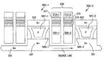
- FIG. 5Aillustrates a first source/drain region 501 and second source/drain region 503 for a non-volatile memory cell 500 formed according to the teachings of the present invention.
- the first and second source/drain regions, 501 and 503are contained in a pillar of semiconductor material, and separated by a body region 507 including channel regions 505 .
- FIGS. 5Aillustrates one such embodiment of the present invention.
- FIG. 5Aillustrates a first source/drain region 501 and second source/drain region 503 for a non-volatile memory cell 500 formed according to the teachings of the present invention.
- the first and second source/drain regions, 501 and 503are contained in a pillar of semiconductor material, and separated by a body region 507 including channel regions 505 .
- the first source/drain region 501is integrally connected to a buried sourceline 525 .
- the buried sourceline 525is be formed of semiconductor material which has the same doping type as the first source/drain region 501 .
- the sourceline 525is formed of semiconductor material of the same doping as the first source/drain region 501 , but is more heavily doped than the first source/drain region 501 .
- a pair of floating gates 509 - 1 and 509 - 2are formed in each trench 530 between adjacent pillars which form memory cells 500 - 1 and 500 - 2 .
- Each one of the pair of floating gates, 509 - 1 and 509 - 2respectively opposes the body regions 507 - 1 and 507 - 2 in adjacent pillars 500 - 1 and 500 - 2 on opposing sides of the trench 530 .
- a single control gate 513is shared by the pair of floating gates 509 - 1 and 509 - 2 on opposing sides of the trench 530 .
- the shared single control gate 513can include an integrally formed control gate line.
- an integrally formed control gate line 513can be one of a plurality of control gate lines which are each independently formed in the trench, such as trench 530 , below the top surface of the pillars 500 - 1 and 500 - 2 and between the pair of floating gates 509 - 1 and 509 - 2 .
- each floating gatee.g. 509 - 1 and 509 - 2 , includes a vertically oriented floating gate having a vertical length of less than 100 nanometers.
- a pair of floating gates 509 - 1 and 509 - 2are formed in each trench 530 between adjacent pillars which form memory cells 500 - 1 and 500 - 2 .
- Each one of the pair of floating gates, 509 - 1 and 509 - 2respectively opposes the body regions 507 - 1 and 507 - 2 in adjacent pillars 500 - 1 and 500 - 2 on opposing sides of the trench 530 .
- each trenche.g. 530
- each trenchhouses a pair of control gate lines, shown as 513 - 1 and 513 - 2 .
- Each one of the pair of control gate lines 513 - 1 and 513 - 2addresses the floating gates, 509 - 1 and 509 - 2 respectively, on opposing sides of the trench 530 .
- the pair of control gate lines, or control gates 513 - 1 and 513 - 2are separated by an insulator layer.
- a pair of floating gates 509 - 1 and 509 - 2are again formed in each trench 530 between adjacent pillars which form memory cells 500 - 1 and 500 - 2 .
- Each one of the pair of floating gates, 509 - 1 and 509 - 2respectively opposes the body regions 507 - 1 and 507 - 2 in adjacent pillars 500 - 1 and 500 - 2 on opposing sides of the trench 530 .
- the plurality of control gate linesare disposed vertically above the floating gates. That is, in one embodiment, the control gate lines are located above the pair of floating gates 509 - 1 and 509 - 2 and not fully beneath the top surface of the pillars 500 - 1 and 500 - 2 . In the embodiment of FIG. 5C , each pair of floating gates, e.g. 509 - 1 and 509 - 2 , in a given trench shares a single control gate line, or control gate 513 .
- a pair of floating gates 509 - 1 and 509 - 2are formed in each trench 530 between adjacent pillars which form memory cells 500 - 1 and 500 - 2 .
- Each one of the pair of floating gates, 509 - 1 and 509 - 2respectively opposes the body regions 507 - 1 and 507 - 2 in adjacent pillars 500 - 1 and 500 - 2 on opposing sides of the trench 530 .
- the plurality of control gate linesare disposed vertically above the floating gates. That is, in one embodiment, the control gate lines are located above the pair of floating gates 509 - 1 and 509 - 2 and not fully beneath the top surface of the pillars 500 - 1 and 500 - 2 . However, in the embodiment of FIG. 5D , each one of the pair of floating gates, e.g. 509 - 1 and 509 - 2 , is addressed by an independent one of the plurality of control lines or control gates, shown in FIG. 5D as 513 - 1 and 513 - 2 .
- a single floating gate 509is formed in each trench 530 between adjacent pillars which form memory cells 500 - 1 and 500 - 2 .
- the single floating gate 509can be either a vertically oriented floating gate 509 or a horizontally oriented floating gate 509 formed by conventional processing techniques, or can be a horizontally oriented floating gate 509 formed by a replacement gate technique such as described in a copending application, entitled “Flash Memory with Ultrathin Vertical Body Transistors,” by Leonard Forbes and Kie Y. Ahn, application Ser. No. 09/780,169.
- the floating gate 509has a vertical length facing the body region 505 of less than 100 nm.
- the floating gate 509has a vertical length facing the body region 505 of less than 50 nm.
- the floating gate 509is shared, respectively, with the body regions 507 - 1 and 507 - 2 , including channel regions 505 - 1 and 505 - 2 , in adjacent pillars 500 - 1 and 500 - 2 located on opposing sides of the trench 530 .
- the control gateincludes a single horizontally oriented control gate line, or control gate 513 formed above the horizontally oriented floating gate 509 .
- the floating gates 509are separated from the control gate lines, or control gates 513 with a low tunnel barrier intergate insulator in accordance with the descriptions given above in connection with FIG. 3 .
- the modifications hereare to use tunneling through the interpoly dielectric to realize flash memory devices.
- the vertical devicesinclude an extra flexibility in that the capacitors, e.g. gate oxide and intergate insulator, are easily fabricated with different areas. This readily allows the use of very high dielectric constant inter-poly dielectric insulators with lower tunneling barriers.
- FIGS. 6A–6Cillustrate that a number of address coincidence schemes can be used together with the present invention.
- FIG. 6Aillustrates a NOR flash memory array 610 having a number of non-volatile memory cells 600 - 1 , 600 - 2 , 6003 , using a coincidence address array scheme.
- FIG. 6Ashows a sourceline 625 coupled to a first source/drain region 601 in each of the number of non-volatile memory cells 600 - 1 , 600 - 2 , 600 - 3 .
- the sourcelineis shown oriented in a first selected direction in the flash memory array 610 .
- FIG. 6Aillustrates a NOR flash memory array 610 having a number of non-volatile memory cells 600 - 1 , 600 - 2 , 6003 , using a coincidence address array scheme.
- FIG. 6Ashows a sourceline 625 coupled to a first source/drain region 601 in each of the number of non-volatile memory cells 600 - 1
- FIG. 6Aa number of control gate lines 630 are shown oriented in a second selected direction in the flash memory array 610 .
- the number of control gate lines 630are coupled to, or integrally formed with the control gates 613 for the number of non-volatile memory cells 600 - 1 , 600 - 2 , 600 - 3 .
- the second selected directionis orthogonal to the first selected direction.
- FIG. 6Ashows a number of bitlines 635 oriented in a third selected direction in the flash memory array 610 . As shown in FIG.
- the number of bitlinesare coupled to the second source/drain regions 603 in the number of non-volatile memory cells 600 - 1 , 600 - 2 , 600 - 3 .
- the third selected directionis parallel to the second selected direction and the number of control gate lines 630 serve as address lines.
- the flash memory array 610includes a number of backgate or substrate/well bias address lines 640 coupled to the substrate.
- FIGS. 6B–6Cillustrate of top view for three different coincidence address scheme layouts suitable for use with the present invention.
- FIG. 6Bprovides the top view layout of the coincidence address scheme described in connection with FIG. 6A .
- FIG. 6Billustrates a number of sourcelines 625 oriented in a first selected direction, a number of control gate lines 630 oriented in a second selected direction, and a number of bitlines 635 oriented in a third selected direction for the flash memory array 600 .
- the first selected direction and the third selected directionare parallel to one another and orthogonal to the second selected direction.
- the number of control gate lines 630serve as address lines.
- the output lines, e.g. bitlines 635are perpendicular to the address lines, e.g. in this embodiment control gate lines 630 .
- FIG. 6Cprovides the top view layout of yet another coincidence address scheme according to the teachings of the present invention.
- FIG. 6Cillustrates a number of sourcelines 625 oriented in a first selected direction, a number of control gate lines 630 oriented in a second selected direction, and a number of bitlines 635 oriented in a third selected direction for the flash memory array 600 .
- the first selected direction and the second selected directionare parallel to one another and orthogonal to the third selected direction.
- the number of bitlines 635serve as output data lines.
- the sourcelines 625can include a uniform ground plane as the same will be known and understood by one of ordinary skill in the art.
- writecan still be achieved by hot electron injection and/or, according to the teachings of the present invention, tunneling from the control gate.
- block eraseis accomplished by driving the control gates with a relatively large positive voltage and tunneling from the metal on top of the floating gate to the metal on the bottom of the control gate.
- FIG. 7Ais an energy band diagram illustrating the band structure at vacuum level with the low tunnel barrier interpoly insulator according to the teachings of the present invention.
- FIG. 7Ais useful in illustrating the reduced tunnel barrier off of the floating gate to the control gate and for illustrating the respective capacitances of the structure according to the teachings of the present invention.
- FIG. 7Ashows the band structure of the silicon substrate, e.g. channel region 701 , silicon dioxide gate insulator, e.g. gate oxide 703 , polysilicon floating gate 705 , the low tunnel barrier interpoly dielectric 707 , between metal plates 709 and 711 , and then the polysilicon control gate 713 , according to the teachings of the present invention.
- the design considerations involvedare determined by the dielectric constant, thickness and tunneling barrier height of the interpoly dielectric insulator 707 relative to that of the silicon dioxide gate insulator, e.g. gate oxide 703 .
- the tunneling probability through the interpoly dielectric 707is an exponential function of both the barrier height and the electric field across this dielectric.
- FIG. 7Bis an energy band diagram illustrating the band structure during an erase operation of electrons from the floating gate 705 to the control gate 713 across the low tunnel barrier interpoly insulator 707 according to the teachings of the present invention.
- FIG. 7Bis similarly useful in illustrating the reduced tunnel barrier off of the floating gate to the control gate and for illustrating the respective capacitances of the structure according to the teachings of the present invention.
- the electric fieldis determined by the total voltage difference across the structure, the ratio of the capacitances (see FIG. 7A ), and the thickness of the interpoly dielectric 707 .
- the lower electric field in the aluminum oxide interpoly insulator 707 for the same current densityreflects the lower tunneling barrier of less than 2 eV, shown in FIG. 7B , as opposed to the 3.2 eV tunneling barrier of silicon oxide 703 , also illustrated in FIG. 7B .
- FIG. 7Cis a graph plotting tunneling currents versus the applied electric fields (reciprocal applied electric field shown) for an number of barrier heights.
- FIG. 7Cillustrates the dependence of the tunneling currents on electric field (reciprocal applied electric field) and barrier height.
- the fraction of voltage across the interpoly or intergate insulator, ⁇ V 2can be increased by making the area of the intergate capacitor, C 2 , (e.g. intergate insulator 707 ) smaller than the area of the transistor gate capacitor, C 1 (e.g. gate oxide 703 ). This would be required with high dielectric constant intergate dielectric insulators 707 and is easily realized with the vertical floating gate structures described above in connection with FIGS. 3 , and 5 A– 5 E.
- the poly-Si layeris to be formed with emphasis on obtaining a surface that is very smooth and morphologically stable at subsequent device processing temperatures which will exceed that used to grow Metal oxide.
- the native SiO x oxide on the poly-Si surfacemust be removed (e.g., by sputter cleaning in an inert gas plasma in situ) just prior to depositing the metal film.
- the electrical characteristics of the resultant Poly-Si/Metal/Metal oxide/Metal/Poly-Si structurewill be better defined and reproducible than that of a Poly-Si/Native SiO x /Metal/Metal oxide/Poly-Si structure.
- the oxide growth rate and limiting thicknesswill increase with oxidation temperature and oxygen pressure.
- the oxidation kinetics of a metalmay, in some cases, depend on the crystallographic orientations of the very small grains of metal which comprise the metal film (see generally, O, Kubaschewski and B. E. Hopkins, “Oxidation of Metals and Alloys”, Butterworth, London, pp. 53–64, 1962). If such effects are significant, the metal deposition process can be modified in order to increase its preferred orientation and subsequent oxide thickness and tunneling uniformity. To this end, use can be made of the fact that metal films strongly prefer to grow during their depositions having their lowest free energy planes parallel to the film surface. This preference varies with the crystal structure of the metal. For example, fcc metals prefer to form ⁇ 111 ⁇ surface plans. Metal orientation effects, if present, would be larger when only a limited fraction of the metal will be oxidized and unimportant when all or most of the metal is oxidized.
- Modifications in the structure shown in FIG. 2may be introduced in order to compensate for certain properties in some metal/oxide/metal layers. Such changes are reasonable since a wide range of metals, alloys and oxides with quite different physical and chemical properties can be used to form these tunnel junctions.
- This oxide barrierhas been studied in detail using Pb/PbO/Pb structures.
- the oxide itselfcan be grown very controllably on deposited lead films using either thermal oxidation (see generally, J. M. Eldridge and J. Matisoo, “Measurement of tunnel current density in a Meal-Oxide-Metal system as a function of oxide thickness,” Proc. 12 th Intern. Conf. on Low Temperature Physics, pp. 427–428, 1971; J. M. Eldridge and D. W. Dong, “Growth of thin PbO layers on lead films. I. Experiment,” Surface Science, Vol. 40, pp. 512–530, 1973) or rf sputter etching in an oxygen plasma (see generally, J.
- Lead and other metal filmscan be deposited by various means including physical sputtering and/or from a Knudsen evaporation cell.
- the sputtering processalso offers the ability to produce smoother films by increasing the re-sputtering-to-deposition ratio since re-sputtering preferentially reduces geometric high points of the film.
- the temperature used to subsequently deposit the Poly-Si control gatemust be held below the melting temperature (327 C) of lead.
- the PbOitself is stable (up to ⁇ 500 C or higher) and thus introduces no temperature constraint on subsequent processes.
- Yet another variation out of severalwould involve: oxidizing the lead film to completion; replacing the top lead electrode with a higher melting metal such as Al; and, then adding the poly-Si control layer. This junction would have asymmetrical tunneling behavior due to the difference in barrier heights between the Pb/PbO and PbO/Al electrodes.
- Tunnel currentsare asymmetrical in this system with somewhat larger currents flowing when electrons are injected from Al/Al 2 O 3 interface developed during oxide growth. This asymmetry is due to a minor change in composition of the growing oxide: there is a small concentration of excess metal in the Al 2 O 3 , the concentration of which diminishes as the oxide is grown thicker. The excess Al +3 ions produce a space charge that lowers the tunnel barrier at the inner interface. The oxide composition at the outer Al 2 O 3 /Al contact is much more stoichiometric and thus has a higher tunnel barrier. In situ ellipsometer measurements on the thermal oxidation of Al films deposited and oxidized in situ support this model (see generally, J. Grimblot and J. M.
- the oxidewill be amorphous and remain so until temperatures in excess of 400 C are reached.
- the initiation of recrystallization and grain growthcan be suppressed, if desired, via the addition of small amounts of glass forming elements (e.g., Si) without altering the growth kinetics or barrier heights significantly.
- Single layers of Ta 2 O 5 , TiO 2 , ZrO 2 , Nb 2 O 5 and similar transition metal oxidescan be formed by “low temperature oxidation” of numerous Transition Metal (e.g., TM oxides) films in molecular and plasma oxygen and also by rf sputtering in an oxygen plasma.
- TM oxidesTransition Metal
- the thermal oxidation kinetics of these metalshave been studied for decades with numerous descriptions and references to be found in the book by Kubaschewski and Hopkins (O. Kubaschewski and B. E. Hopkins, “Oxidation of Metals and Alloys”, Butterworth, London, pp. 53–64, 1962).
- Such metalsoxidize via logarithmic kinetics to reach thicknesses of a few to several tens of angstroms in the range of 100 to 300 C.
- Excellent oxide barriers for Josephson tunnel devicescan be formed by rf sputter etching these metals in an oxygen plasma (see generally, J. M. Greiner, “Josephson tunneling barriers by rf sputter etching in an oxygen plasma,” J. Appl. Phys., Vol. 42, No. 12, pp. 5151–5155, 1971; O. Michikami et al., “Method of fabrication of Josephson tunnel junctions,” U.S. Pat. No. 4,412,902, Nov. 1, 1983).
- Such “low temperature oxidation” approachesdiffer considerably from MOCVD processes used to produce these TM oxides.
- MOCVD filmsrequire high temperature oxidation treatments to remove carbon impurities, improve oxide stoichiometry and produce recrystallization. Such high temperature treatments also cause unwanted interactions between the oxide and the underlying silicon and thus have necessitated the introduction of interfacial barrier layers. See, for example, H. F. Luan et al., “High quality Ta 2 O 5 gate dielectrics with T ox,eq ⁇ 10 angstroms,” IEDM Tech. Digest, pp. 141–144, 1999.
- this treatmentcan be carried out in an inert gas atmosphere, thus lessening the possibility of inadvertently oxidizing the poly-Si floating gate.
- This earlier disclosurewas directed at developing methods and procedures for producing high dielectric constant films for storage cells for DRAMs, the same teachings can be applied to producing thinner metal oxide tunnel films for the flash memory devices described in this disclosure.
- the dielectric constants of these TM oxidesare substantially greater (>25 to 30 or more) than those of PbO and Al 2 O 3 .
- Duplex layers of these high dielectric constant oxide filmsare easily fabricated with simple tools and also provide improvement in device yields and reliability. Each oxide layer will contain some level of defects but the probability that such defects will overlap is exceedingly small.
- Thinner TM layerswill be used in this invention relative to those used to form DRAMs. Unlike DRAMs where leakage must be eliminated, the duplex oxides used here must be thin enough to carry very controlled levels of current flow when subjected to reasonable applied fields and times.
- TM and their oxidesare highly refractory and etchable (e.g., by RIE). Hence they are quite compatible with poly-Si control gate processes and other subsequent steps.
- a stack of oxide filmshaving quite different properties, for example, a stack comprised of a high dielectric constant (k) oxide/ a low k oxide/ a high k oxide.
- Low temperature oxidationcan be used to form numerous variations of such structures. While most of this disclosure deals with the formation and use of stacks of oxide dielectrics, it is also possible to use “low temperature oxidation” to form other thin film dielectrics such as nitrides, oxynitrides, etc. that could provide additional functions such as being altered by monochromatic light, etc. These will not be discussed further here.
- the dielectric constants of crystallized, perovskite oxidescan be very large, with values in the 100 to 1000 or more range.
- the basic processis more complicated than that needed to oxidize layered films of transition metals.
- the TM layerswould typically be pure metals although they could be alloyed.
- the TMsare similar metallurgically as are their oxides.
- the parent alloy films that can be converted to a perovskite oxideare typically comprised of metals having widely different chemical reactivities with oxygen and other common gasses.
- Y—Ba—Cu system referenced aboveY and Ba are among the most reactive of metals while the reactivity of Cu approaches (albeit distantly) those of other noble metals.
- the alloyis to be completely oxidized, then thin film barriers such as Pd, Pt, etc. or their conductive oxides must be added between the Si and the parent metal film to serve as: electrical contact layers; diffusion barriers; and, oxidation stops.
- the Schottky barrier heights of various TM oxides and perovskite oxides in contact with various metalswill help in the design of the tunnel device.
- the barrier heightswill represent that developed during oxide growth at the parent perovskite alloy/perovskite oxide interface. Obviously, such barrier heights cannot be predicted ab initio for such a wide class of materials but will have to be developed as the need arises. This information will have to be developed on a system-by-system basis.
- Writecan be achieved by the normal channel hot electron injection and gate current through the silicon oxide to the floating gate. This is done by selecting a particular column by applying a high control gate voltage and applying relatively large drain voltage as is done with conventional ETOX flash memory devices.
- writecan also be accomplished by applying a positive voltage to the substrate or well select line and a large negative voltage to the control gates, electrons will tunnel from the control gate to the floating gate.
- the low tunnel barrierwill provide an easy write operation and the selection of the substrate or well bias will provide selectivity and address only one device.
- eraseis achieved by providing a negative voltage to the substrate or well address line and a large positive voltage to the control gate. This causes electrons to tunnel off of the floating gate on to the control gate.
- a whole rowcan be erased by addressing all the column lines along that row and a block can be erased by addressing multiple row back gate or substrate/well address lines.
- Readis accomplished as in conventional ETOX flash memory devices.
- a column lineis addressed by applying a positive control gate voltage and sensing the current along the data bit or drain row address line.
- FIG. 8shows a conventional NOR decode array 800 for memory circuits.
- the address linesare A 1 through A 3 and inverse address lines, ⁇ overscore (A 1 ) ⁇ through ⁇ overscore (A 3 ) ⁇ .
- the conventional NOR decode arrayis programmable at the gate mask level by either fabricating a thin oxide gate transistor, e.g. transistors 801 - 1 , 801 - 2 , . . . , 801 -N, at the intersection of lines in the array or not fabricating a thin oxide gate transistor, e.g. missing thin oxide transistors, 802 - 1 , 802 - 2 , . . . , 802 -N, at such an intersection.
- a thin oxide gate transistore.g. transistors 801 - 1 , 801 - 2 , . . . , 802 -N, at such an intersection.
- NMOS transistors816 are used as load devices.
- each of the row lines 814acts as a NOR gate for the address lines A 1 through A 3 and inverse address lines, ⁇ overscore (A 1 ) ⁇ through ⁇ overscore (A 3 ) ⁇ that are connected to the row lines 814 through the thin oxide gate transistor, e.g. transistors 801 - 1 , 801 - 2 , . . . , 801 -N, of the array. That is, row line R 1 is maintained at a high potential, +VDD, in the positive logic NMOS decode array shown in FIG. 8A , unless one or more of the thin oxide gate transistor, e.g. transistors 801 - 1 , 801 - 2 , . . .
- each thin oxide gate transistore.g. transistors 801 - 1 , 801 - 2 , . . . , 801 -N, conducts, or is turned “on.” This conduction of the thin oxide gate transistor, e.g.
- transistors 801 - 1 , 801 - 2 , . . . , 801 -Nperforms the NOR positive logic circuit function
- an inversion of the OR circuit functionresults from inversion of data onto the row lines 814 through the thin oxide gate transistor, e.g. transistors 801 - 1 , 801 - 2 , . . . , 801 -N, of the array, in order to output a low logic level signal on the row lines 814 .
- a particular row line 814is addressed when none of the thin oxide gate transistor, e.g. transistors 801 - 1 , 801 - 2 , . . . , 801 -N, coupled to that row line 814 are turned “on.”
- the incoming address on each lineis inverted and the combination of the original address and inverted or complemented values used to drive the gates of transistors in the decode array 800 .
- the transistors 801 - 1 , 801 - 2 , . . . , 801 -N in the array 800are enhancement mode NMOS devices and depletion mode NMOS transistors are used as load devices 816 . All voltages are positive in a simple NMOS circuit. This is a positive logic NOR decode array, the logic one state, “1” is the most positive voltage, +VDD, and the logic level zero, “0” is the least positive voltage or ground.
- the transistors used in FIG. 8are NMOS driver transistors with a depletion mode NMOS load technology.
- the load device or NMOS load transistoris a depletion mode or normally “on” transistor which acts as a constant current source during the pull up switching transient thus providing high switching speed.
- the driver transistoris an enhancement mode NMOS transistor which is normally “off” with zero gate bias.
- FIG. 9is a schematic diagram illustrating one embodiment of a decode circuit, or memory address decoder, 900 according to the teachings of the present invention.
- the address linesare A 1 through A 3 and inverse address lines, ⁇ overscore (A 1 ) ⁇ through ⁇ overscore (A 3 ) ⁇ .
- the decode circuit 900is programmable at the gate mask level by either fabricating a driver transistor, or logic cell, e.g. transistors 901 - 1 , 901 - 2 , . . . , 901 -N, at the intersection of lines in the array or not fabricating a driver transistor, or logic cell, e.g.
- fabricating a driver transistore.g. transistors 901 - 1 , 901 - 2 , . . . , 901 -N, at the intersection of lines in the array includes fabricating the floating gate driver transistor according to the embodiments discussed and described in detail in connection with FIGS. 5 and 6 .
- a number of p-channel metal oxide semiconductor (PMOS) load transistors, 916are used as load devices and are coupled to the output lines, or row lines, 914 , of the decode circuit 900 .
- PMOSmetal oxide semiconductor
- the incoming address on each address line A 1 through A 3is inverted and the combination of the original address on each address line A 1 through A 3 and inverted or complemented values on inverse address lines, ⁇ overscore (A 1 ) ⁇ through ⁇ overscore (A 3 ) ⁇ , used to drive the control gates of transistors 901 - 1 , 901 - 2 , . . . , 901 -N in the decode array 900 .
- the floating gate driver transistors, or logic cells, e.g. transistors 901 - 1 , 901 - 2 , . . . , 901 -N in the decode array 900are n-channel floating gate driver transistors having a low tunnel barrier intergate insulator between the control gate and floating gate as described above in connection with FIGS. 5 and 6 .
- each of the row lines 914acts as a NOR gate for the address lines A 1 through A 3 and inverse address lines, ⁇ overscore (A 1 ) ⁇ through ⁇ overscore (A 3 ) ⁇ that are connected to the row lines 914 through the floating gate driver transistors, or logic cells, e.g. transistors 901 - 1 , 901 - 2 , . . . , 901 -N, of the array 900 . That is, row line R 1 is maintained at a high potential VDD, or logic “1” unless one or more of the floating gate driver transistors, or logic cells, e.g. transistors 901 - 1 , 901 - 2 , . . .
- a logic “1”, or VDD, on one of the address lines A 1 through A 3 or inverse address lines, ⁇ overscore (A 1 ) ⁇ through ⁇ overscore (A 3 ) ⁇is required in order to turn on one of the n-channel floating gate driver transistors, or logic cells, e.g. transistors 901 - 1 , 901 - 2 , . . .
- the floating gate driver transistors, or logic cellse.g. transistors 901 - 1 , 901 - 2 , . . . , 901 -N, can be programmed to have two different conductivity states depending upon whether electrons are stored on the floating gate.
- the floating gate transistoris effectively removed from the programmable memory address and decode circuit 900 .
- the driver transistorse.g. transistors 901 - 1 , 901 - 2 , . . . , 901 -N in the array are floating gate transistor devices.
- the floating gate driver transistors 9011 , 901 - 2 , . . . , 901 -Nare formed according to the embodiments of the present invention as disclosed and described in detail in connection with FIGS. 5 and 6 . In this manner, the floating gate driver transistors, 901 - 1 , 901 - 2 , . . .
- the load devices 916shown in the address decoder 900 of FIG. 9 , are p-channel metal oxide semiconductor (PMOS) transistors and not depletion mode n-channel transistors as is more usual.
- PMOSmetal oxide semiconductor
- the decode circuit 900 embodiment of the present invention shown in FIG. 9is formed according to a CMOS process and can be referred to as a CMOS decode array 900 .
- the decode circuit 900 of the present inventionincludes at least one redundant row line, RD.
- a number of additional floating gate driver transistorse.g. transistors T 1 –T 6 , are provided in the array coupled to address lines A 1 through A 3 or inverse address lines, ⁇ overscore (A 1 ) ⁇ through ⁇ overscore (A 3 ) ⁇ and the redundant row line, RD.
- these additional driver transistorse.g. transistors T 1 –T 6 , are formed according to the embodiments described and discussed in detail above in connection with FIGS. 5 and 6 .
- the additional floating gate driver transistors, T 1 –T 6will have a vertical control gate formed by the address lines A 1 through A 3 or inverse address lines, ⁇ overscore (A 1 ) ⁇ through ⁇ overscore (A 3 ) ⁇ .
- the additional floating gate driver transistors, T 1 –T 6will have a horizontal control gate formed by the address lines A 1 through A 3 or inverse address lines, ⁇ overscore (A 1 ) ⁇ through ⁇ overscore (A 3 ) ⁇ located above the floating gates of the floating gate driver transistors, T 1 –T 6 .
- the second source/drain region for the additional driver transistors, T 1 –T 6are coupled to the at least one redundant row line, or wordline, RD.
- a p-channel metal oxide semiconductor (PMOS) load transistor T 7similar to p-channel metal oxide semiconductor (PMOS) load transistors 916 is coupled to the at least one redundant row line, RD as well to complete the CMOS inverter configuration.
- these non volatile, floating gate driver transistorscan be programmed to have two different conductivity states depending upon whether electrons are stored on the vertical floating gate.
- the floating gate transistoris effectively removed from the programmable memory address and decode circuits 900 of the present invention.
- the implementation of these floating gate driver transistors, e.g. transistors T 1 –T 6 , in the decode circuit 900 of the present invention,enables error correction for replacing a row, or column in the array as one of ordinary skill in the art will understand upon reading this disclosure.
- redundant row linese.g. redundant row line RD
- redundant row line RDavailable to replace or error correct for row lines 914 , which are determined defective or which have failed in the field.
- the present inventionis usable to provide such error correction by replacing a row, or column, in a memory decode circuit 900 .
- the floating gate driver transistors, T 1 –T 6have no charge stored on the floating gate they will function as normal inverters for the decode circuit 900 . Conversely, if there is a charge stored charge on the floating gate, the conductivity of the floating gate driver transistors, T 1 –T 6 , will not become high enough and will not function as a driver transistor. In this latter case, the output for the redundant row line RD in the decode circuit 900 of the present invention will not change charge states. Hence, if there is a charge stored on the vertical floating gate of the floating gate driver transistors, T 1 –T 6 , the drivers are effectively removed from the decode circuits 900 .
- the decode circuit shown in FIG. 9can represent a column decode circuit 900 .
- the lines 914 or redundant line RDwhich are coupled to the address lines A 1 through A 3 or inverse address lines, ⁇ overscore (A 1 ) ⁇ through ⁇ overscore (A 3 ) ⁇ through the floating gate driver transistors, 901 - 1 , 901 - 2 , . . . , 901 -N and T 1 –T 6 , can be complementary bit lines for column decoding as the same will be know and understood by one of ordinary skill in the art.
- inverterscan be used as necessary to affect the transition from one logic system, e.g. positive logic system, to a negative logic system while still capitalizing on the utility of the novel floating gate driver transistors 901 - 1 , 901 - 2 , . . . , 901 -N and T 1 –T 6 , having a low tunnel barrier intergate insulator between the control gate and floating gate in decode circuit 900 . If the floating gate in a floating gate driver transistor is programmed with a negative charge on the floating gate it will not be active in the array and it is effectively removed from the array.
- the field programmable, in service or in circuit programmable, logic devices described herework with much lower voltages than the normal devices used in current in field, or in service, programmable decode circuit technology due to tunneling of charge between the floating gate and control gate through the low-tunnel barrier intergate insulator. They can be programmed with Voltages of 2.0 to 4.0 Volts and the normal operating voltages on the vertical control gates can be of the order 1.0 Volt or so.
- the absence of presence of stored charge on the floating gatesis read by addressing the x-address or control gate lines and y-column/sourcelines to form a coincidence in address at a particular floating gate.
- the control gate linewould for instance be driven positive at some voltage of 1.0 Volts and the y-column/sourceline grounded, if the floating gate is not charged with electrons then the floating transistor would turn on tending to hold the row or word address line on that particular row down indicating the presence of a stored “one” in the cell. If this particular floating gate is charged with stored electrons, the transistor will not turn on and the presence of a stored “zero” indicated in the cell. In this manner, data stored on a particular floating gate can be read.
- datais read out in “bit pairs” by addressing not only a single floating gate but rather both of the floating gates in row adjacent pillars on each side of a particular control gate address line.
- Datais stored into the cell by hot electron injection or alternatively, according to the teachings of the present invention, by tunneling charge from the control gate to the floating gate through the low-tunnel barrier intergate insulator. Erasure is accomplished by driving the control gate line with a positive voltage and the sourceline, or backgate/substrate well address line, of the transistor with a negative bias so the total voltage difference is in the order of 2 Volts causing electrons to tunnel off of the floating gates and to the control gates.
- datacan be erased in “bit pairs” since both floating gates on each side of a control gate can be erased at the same time.
- This architectureis amenable to block address schemes where sections of the array are erased and reset at the same time.
- FIG. 10is a simplified block diagram of a high-level organization of an electronic system 1001 according to the teachings of the present invention.
- the electronic system 1001is a system whose functional elements consist of an arithmetic/logic unit (ALU) 1020 or processor 1020 , a control unit 1030 , a memory device unit 1040 and an input/output (I/O) device 1050 .
- ALUarithmetic/logic unit
- processor 1020the electronic system 1001
- control unit 1030the control unit 1030
- memory device unit 1040an input/output
- I/Oinput/output
- Such an electronic system 1001will have a native set of instructions that specify operations to be performed on data by the ALU 1020 and other interactions between the ALU 1020 , the memory device unit 1040 and the I/O devices 1050 .
- the memory device units 1040contain the data plus a stored list of instructions.
- the control unit 1030coordinates all operations of the processor 1020 , the memory device 1040 and the I/O devices 1050 by continuously cycling through a set of operations that cause instructions to be fetched from the memory device 1040 and executed.
- Memory device 1040can be implemented with “in-service” programmable low voltage decode circuits, according to the teachings of the present invention, e.g., having a low-tunnel barrier intergate insulator between the control gate and floating gate.
- the decode circuits of the present inventioncan enable error correction by replacing a row, or column, in a memory array.
- the low tunnel barrier interpoly insulators of the present inventionavoid the large barriers to electron tunneling or hot electron injection presented by the silicon oxide-silicon interface, 3.2 eV, which result in slow write and erase speeds even at very high electric fields.
- the present inventionalso avoids the combination of very high electric fields and damage by hot electron collisions in the which oxide result in a number of operational problems like soft erase error, reliability problems of premature oxide breakdown and a limited number of cycles of write and erase.
- the low tunnel barrier interpoly dielectric insulator erase approach, of the present inventionremedies the above mentioned problems of having a rough top surface on the polysilicon floating gate which results in, poor quality interpoly oxides, sharp points, localized high electric fields, premature breakdown and reliability problems.
- any arbitrary combinational logic functioncan be realized in the so-called sum-of-products form.
- a sum of productsmay be implemented by using a two level logic configuration such as the NOR-NOR arrays shown in FIG. 10 , or by a combination of NOR gates and NAND gates.
- a NAND gatecan be realized by a NOR gate with the inputs inverted.
Landscapes
- Engineering & Computer Science (AREA)
- Microelectronics & Electronic Packaging (AREA)
- Non-Volatile Memory (AREA)
- Semiconductor Memories (AREA)
Abstract
Description
J=Bexp(−Eo/E)
where E is the electric field across the interpoly
- (i) Insert certain metals at the TM/poly-Si boundaries that will prevent inter-diffusion of the TM and the poly-Si.
- (ii) Completely oxide the TMs. The electrical characteristics of the resulting poly-Si/
TM oxide 1/TM oxide 2/poly-Si structure will be different in the absence of having TM at the oxide/metal interfaces.
Claims (31)
Priority Applications (2)
| Application Number | Priority Date | Filing Date | Title |
|---|---|---|---|
| US09/945,500US7075829B2 (en) | 2001-08-30 | 2001-08-30 | Programmable memory address and decode circuits with low tunnel barrier interpoly insulators |
| US10/931,711US7187587B2 (en) | 2001-08-30 | 2004-09-01 | Programmable memory address and decode circuits with low tunnel barrier interpoly insulators |
Applications Claiming Priority (1)
| Application Number | Priority Date | Filing Date | Title |
|---|---|---|---|
| US09/945,500US7075829B2 (en) | 2001-08-30 | 2001-08-30 | Programmable memory address and decode circuits with low tunnel barrier interpoly insulators |
Related Child Applications (1)
| Application Number | Title | Priority Date | Filing Date |
|---|---|---|---|
| US10/931,711DivisionUS7187587B2 (en) | 2001-08-30 | 2004-09-01 | Programmable memory address and decode circuits with low tunnel barrier interpoly insulators |
Publications (2)
| Publication Number | Publication Date |
|---|---|
| US20030043632A1 US20030043632A1 (en) | 2003-03-06 |
| US7075829B2true US7075829B2 (en) | 2006-07-11 |
Family
ID=25483184
Family Applications (2)
| Application Number | Title | Priority Date | Filing Date |
|---|---|---|---|
| US09/945,500Expired - Fee RelatedUS7075829B2 (en) | 2001-08-30 | 2001-08-30 | Programmable memory address and decode circuits with low tunnel barrier interpoly insulators |
| US10/931,711Expired - LifetimeUS7187587B2 (en) | 2001-08-30 | 2004-09-01 | Programmable memory address and decode circuits with low tunnel barrier interpoly insulators |
Family Applications After (1)
| Application Number | Title | Priority Date | Filing Date |
|---|---|---|---|
| US10/931,711Expired - LifetimeUS7187587B2 (en) | 2001-08-30 | 2004-09-01 | Programmable memory address and decode circuits with low tunnel barrier interpoly insulators |
Country Status (1)
| Country | Link |
|---|---|
| US (2) | US7075829B2 (en) |
Cited By (27)
| Publication number | Priority date | Publication date | Assignee | Title |
|---|---|---|---|---|
| US20030040157A1 (en)* | 2001-08-24 | 2003-02-27 | Leonard Forbes | Vertical transistor with horizontal gate layers |
| US20040160830A1 (en)* | 2001-08-30 | 2004-08-19 | Micron Technology, Inc. | DRAM cells with repressed floating gate memory, low tunnel barrier interpoly insulators |
| US20050024945A1 (en)* | 2001-08-30 | 2005-02-03 | Micron Technology, Inc. | Programmable memory address and decode circuits with low tunnel barrier interpoly insulators |
| US20050023603A1 (en)* | 2001-08-30 | 2005-02-03 | Micron Technology, Inc. | Atomic layer deposition of metal oxide and/or low asymmetrical tunnel barrier interpoly insulators |
| US20050169054A1 (en)* | 2001-08-30 | 2005-08-04 | Micron Technology, Inc. | SRAM cells with repressed floating gate memory, low tunnel barrier interpoly insulators |
| US20070105313A1 (en)* | 2001-08-30 | 2007-05-10 | Micron Technology, Inc. | In service programmable logic arrays with low tunnel barrier interpoly insulators |
| US20070170492A1 (en)* | 2005-02-23 | 2007-07-26 | Micron Technology, Inc. | Germanium-silicon-carbide floating gates in memories |
| US7410910B2 (en) | 2005-08-31 | 2008-08-12 | Micron Technology, Inc. | Lanthanum aluminum oxynitride dielectric films |
| US20080308857A1 (en)* | 2007-06-13 | 2008-12-18 | Macronix International Co., Ltd. | Systems and Methods for Self Convergence During Erase of a Non-Volatile Memory Device |
| US7545674B2 (en) | 2001-08-30 | 2009-06-09 | Micron Technology, Inc. | Flash memory with low tunnel barrier interpoly insulators |
| US7554161B2 (en) | 2002-06-05 | 2009-06-30 | Micron Technology, Inc. | HfAlO3 films for gate dielectrics |
| US20090174010A1 (en)* | 2008-01-03 | 2009-07-09 | International Business Machines Corporation | Sram device structure including same band gap transistors having gate stacks with high-k dielectrics and same work function |
| US7560395B2 (en) | 2005-01-05 | 2009-07-14 | Micron Technology, Inc. | Atomic layer deposited hafnium tantalum oxide dielectrics |
| US7572695B2 (en) | 2005-05-27 | 2009-08-11 | Micron Technology, Inc. | Hafnium titanium oxide films |
| US7575978B2 (en) | 2005-08-04 | 2009-08-18 | Micron Technology, Inc. | Method for making conductive nanoparticle charge storage element |
| US7588988B2 (en) | 2004-08-31 | 2009-09-15 | Micron Technology, Inc. | Method of forming apparatus having oxide films formed using atomic layer deposition |
| US7589029B2 (en) | 2002-05-02 | 2009-09-15 | Micron Technology, Inc. | Atomic layer deposition and conversion |
| US7625794B2 (en) | 2003-03-31 | 2009-12-01 | Micron Technology, Inc. | Methods of forming zirconium aluminum oxide |
| US7670646B2 (en) | 2002-05-02 | 2010-03-02 | Micron Technology, Inc. | Methods for atomic-layer deposition |
| US7687409B2 (en) | 2005-03-29 | 2010-03-30 | Micron Technology, Inc. | Atomic layer deposited titanium silicon oxide films |
| US7719065B2 (en) | 2004-08-26 | 2010-05-18 | Micron Technology, Inc. | Ruthenium layer for a dielectric layer containing a lanthanide oxide |
| US20110012629A1 (en)* | 2009-07-15 | 2011-01-20 | International Business Machines Corporation | Replacement-gate-compatible programmable electrical antifuse |
| US7927948B2 (en) | 2005-07-20 | 2011-04-19 | Micron Technology, Inc. | Devices with nanocrystals and methods of formation |
| US7989290B2 (en) | 2005-08-04 | 2011-08-02 | Micron Technology, Inc. | Methods for forming rhodium-based charge traps and apparatus including rhodium-based charge traps |
| US8110469B2 (en) | 2005-08-30 | 2012-02-07 | Micron Technology, Inc. | Graded dielectric layers |
| US9136457B2 (en) | 2006-09-20 | 2015-09-15 | Hypres, Inc. | Double-masking technique for increasing fabrication yield in superconducting electronics |
| US9741920B1 (en) | 2010-01-08 | 2017-08-22 | Hypres, Inc. | System and method for providing multi-conductive layer metallic interconnects for superconducting integrated circuits |
Families Citing this family (23)
| Publication number | Priority date | Publication date | Assignee | Title |
|---|---|---|---|---|
| US7012297B2 (en)* | 2001-08-30 | 2006-03-14 | Micron Technology, Inc. | Scalable flash/NV structures and devices with extended endurance |
| US7135734B2 (en)* | 2001-08-30 | 2006-11-14 | Micron Technology, Inc. | Graded composition metal oxide tunnel barrier interpoly insulators |
| US6784480B2 (en)* | 2002-02-12 | 2004-08-31 | Micron Technology, Inc. | Asymmetric band-gap engineered nonvolatile memory device |
| US7221586B2 (en) | 2002-07-08 | 2007-05-22 | Micron Technology, Inc. | Memory utilizing oxide nanolaminates |
| US7192892B2 (en)* | 2003-03-04 | 2007-03-20 | Micron Technology, Inc. | Atomic layer deposited dielectric layers |
| IL161869A (en) | 2004-05-06 | 2014-05-28 | Serconet Ltd | System and method for carrying a wireless based signal over wiring |
| US7279740B2 (en) | 2005-05-12 | 2007-10-09 | Micron Technology, Inc. | Band-engineered multi-gated non-volatile memory device with enhanced attributes |
| US7402850B2 (en)* | 2005-06-21 | 2008-07-22 | Micron Technology, Inc. | Back-side trapped non-volatile memory device |
| US7829938B2 (en)* | 2005-07-14 | 2010-11-09 | Micron Technology, Inc. | High density NAND non-volatile memory device |
| US7629641B2 (en)* | 2005-08-31 | 2009-12-08 | Micron Technology, Inc. | Band engineered nano-crystal non-volatile memory device utilizing enhanced gate injection |
| US7429767B2 (en)* | 2005-09-01 | 2008-09-30 | Micron Technology, Inc. | High performance multi-level non-volatile memory device |
| US7813451B2 (en)* | 2006-01-11 | 2010-10-12 | Mobileaccess Networks Ltd. | Apparatus and method for frequency shifting of a wireless signal and systems using frequency shifting |
| US7633801B2 (en)* | 2007-06-21 | 2009-12-15 | Micron Technology, Inc. | Memory in logic cell |
| US8594133B2 (en) | 2007-10-22 | 2013-11-26 | Corning Mobileaccess Ltd. | Communication system using low bandwidth wires |
| US8175649B2 (en) | 2008-06-20 | 2012-05-08 | Corning Mobileaccess Ltd | Method and system for real time control of an active antenna over a distributed antenna system |
| US7973357B2 (en)* | 2007-12-20 | 2011-07-05 | Samsung Electronics Co., Ltd. | Non-volatile memory devices |
| WO2010089719A1 (en) | 2009-02-08 | 2010-08-12 | Mobileaccess Networks Ltd. | Communication system using cables carrying ethernet signals |
| US8829592B2 (en)* | 2010-12-14 | 2014-09-09 | Intel Corporation | Non-volatile storage element having dual work-function electrodes |
| EP2829152A2 (en) | 2012-03-23 | 2015-01-28 | Corning Optical Communications Wireless Ltd. | Radio-frequency integrated circuit (rfic) chip(s) for providing distributed antenna system functionalities, and related components, systems, and methods |
| US9184960B1 (en) | 2014-09-25 | 2015-11-10 | Corning Optical Communications Wireless Ltd | Frequency shifting a communications signal(s) in a multi-frequency distributed antenna system (DAS) to avoid or reduce frequency interference |
| JP6753450B2 (en)* | 2018-11-12 | 2020-09-09 | セイコーエプソン株式会社 | Substrates for electro-optical devices, electro-optic devices, electronic devices |
| JP7525405B2 (en)* | 2019-01-25 | 2024-07-30 | 株式会社半導体エネルギー研究所 | Semiconductor Device |
| US11049807B2 (en) | 2019-09-25 | 2021-06-29 | Sandisk Technologies Llc | Three-dimensional memory device containing tubular blocking dielectric spacers |
Citations (110)
| Publication number | Priority date | Publication date | Assignee | Title |
|---|---|---|---|---|
| US3978577A (en) | 1975-06-30 | 1976-09-07 | International Business Machines Corporation | Fixed and variable threshold N-channel MNOSFET integration technique |
| US4295150A (en) | 1978-10-18 | 1981-10-13 | Itt Industries, Inc. | Storage transistor |
| US4412902A (en) | 1981-06-22 | 1983-11-01 | Nippon Telegraph & Telephone Public Corporation | Method of fabrication of Josephson tunnel junction |
| US4449205A (en) | 1982-02-19 | 1984-05-15 | International Business Machines Corp. | Dynamic RAM with non-volatile back-up storage and method of operation thereof |
| US4495219A (en) | 1981-10-09 | 1985-01-22 | Fujitsu Limited | Process for producing dielectric layers for semiconductor devices |
| US4556975A (en) | 1983-02-07 | 1985-12-03 | Westinghouse Electric Corp. | Programmable redundancy circuit |
| US4672240A (en) | 1983-02-07 | 1987-06-09 | Westinghouse Electric Corp. | Programmable redundancy circuit |
| US4688078A (en) | 1982-09-30 | 1987-08-18 | Ning Hseih | Partially relaxable composite dielectric structure |
| US4717943A (en) | 1984-06-25 | 1988-01-05 | International Business Machines | Charge storage structure for nonvolatile memories |
| US4757360A (en) | 1983-07-06 | 1988-07-12 | Rca Corporation | Floating gate memory device with facing asperities on floating and control gates |
| US4780424A (en) | 1987-09-28 | 1988-10-25 | Intel Corporation | Process for fabricating electrically alterable floating gate memory devices |
| US4794565A (en) | 1986-09-15 | 1988-12-27 | The Regents Of The University Of California | Electrically programmable memory device employing source side injection |
| US4870470A (en) | 1987-10-16 | 1989-09-26 | International Business Machines Corporation | Non-volatile memory cell having Si rich silicon nitride charge trapping layer |
| US4939559A (en) | 1981-12-14 | 1990-07-03 | International Business Machines Corporation | Dual electron injector structures using a conductive oxide between injectors |
| US5042011A (en) | 1989-05-22 | 1991-08-20 | Micron Technology, Inc. | Sense amplifier pulldown device with tailored edge input |
| US5071782A (en) | 1990-06-28 | 1991-12-10 | Texas Instruments Incorporated | Vertical memory cell array and method of fabrication |
| US5073519A (en) | 1990-10-31 | 1991-12-17 | Texas Instruments Incorporated | Method of fabricating a vertical FET device with low gate to drain overlap capacitance |
| US5153880A (en) | 1990-03-12 | 1992-10-06 | Xicor, Inc. | Field-programmable redundancy apparatus for memory arrays |
| US5280205A (en) | 1992-04-16 | 1994-01-18 | Micron Technology, Inc. | Fast sense amplifier |
| US5350738A (en) | 1991-03-27 | 1994-09-27 | International Superconductivity Technology Center | Method of manufacturing an oxide superconductor film |
| US5353431A (en) | 1991-04-29 | 1994-10-04 | Intel Corporation | Memory address decoder with storage for memory attribute information |
| US5399516A (en) | 1992-03-12 | 1995-03-21 | International Business Machines Corporation | Method of making shadow RAM cell having a shallow trench EEPROM |
| US5418389A (en) | 1992-11-09 | 1995-05-23 | Mitsubishi Chemical Corporation | Field-effect transistor with perovskite oxide channel |
| US5445984A (en) | 1994-11-28 | 1995-08-29 | United Microelectronics Corporation | Method of making a split gate flash memory cell |
| US5455792A (en) | 1994-09-09 | 1995-10-03 | Yi; Yong-Wan | Flash EEPROM devices employing mid channel injection |
| US5474947A (en) | 1993-12-27 | 1995-12-12 | Motorola Inc. | Nonvolatile memory process |
| US5488612A (en) | 1993-10-04 | 1996-01-30 | International Business Machines, Corporation | Method and apparatus for field testing field programmable logic arrays |
| US5497494A (en) | 1993-07-23 | 1996-03-05 | International Business Machines Corporation | Method for saving and restoring the state of a CPU executing code in protected mode |
| US5498558A (en) | 1994-05-06 | 1996-03-12 | Lsi Logic Corporation | Integrated circuit structure having floating electrode with discontinuous phase of metal silicide formed on a surface thereof and process for making same |
| US5508544A (en) | 1992-12-14 | 1996-04-16 | Texas Instruments Incorporated | Three dimensional FAMOS memory devices |
| US5510278A (en) | 1994-09-06 | 1996-04-23 | Motorola Inc. | Method for forming a thin film transistor |
| US5600592A (en) | 1993-05-28 | 1997-02-04 | Kabushiki Kaisha Toshiba | Nonvolatile semiconductor memory device having a word line to which a negative voltage is applied |
| US5617351A (en) | 1992-03-12 | 1997-04-01 | International Business Machines Corporation | Three-dimensional direct-write EEPROM arrays and fabrication methods |
| US5619642A (en) | 1994-12-23 | 1997-04-08 | Emc Corporation | Fault tolerant memory system which utilizes data from a shadow memory device upon the detection of erroneous data in a main memory device |
| US5618575A (en) | 1992-07-02 | 1997-04-08 | Balzers Aktiengesellschaft | Process and apparatus for the production of a metal oxide layer |
| US5627785A (en) | 1996-03-15 | 1997-05-06 | Micron Technology, Inc. | Memory device with a sense amplifier |
| US5646430A (en) | 1991-08-30 | 1997-07-08 | Texas Instruments Incorporated | Non-volatile memory cell having lightly-doped source region |
| US5677867A (en) | 1991-06-12 | 1997-10-14 | Hazani; Emanuel | Memory with isolatable expandable bit lines |
| US5691230A (en) | 1996-09-04 | 1997-11-25 | Micron Technology, Inc. | Technique for producing small islands of silicon on insulator |
| US5691209A (en)* | 1995-09-14 | 1997-11-25 | Liberkowski; Janusz B. | Lattice interconnect method and apparatus for manufacturing multi-chip modules |
| US5739544A (en)* | 1993-05-26 | 1998-04-14 | Matsushita Electric Industrial Co., Ltd. | Quantization functional device utilizing a resonance tunneling effect and method for producing the same |
| US5801401A (en) | 1997-01-29 | 1998-09-01 | Micron Technology, Inc. | Flash memory with microcrystalline silicon carbide film floating gate |
| US5852306A (en) | 1997-01-29 | 1998-12-22 | Micron Technology, Inc. | Flash memory with nanocrystalline silicon film floating gate |
| US5880991A (en) | 1997-04-14 | 1999-03-09 | International Business Machines Corporation | Structure for low cost mixed memory integration, new NVRAM structure, and process for forming the mixed memory and NVRAM structure |
| US5923056A (en) | 1996-10-10 | 1999-07-13 | Lucent Technologies Inc. | Electronic components with doped metal oxide dielectric materials and a process for making electronic components with doped metal oxide dielectric materials |
| US5936274A (en) | 1997-07-08 | 1999-08-10 | Micron Technology, Inc. | High density flash memory |
| US5952692A (en) | 1996-11-15 | 1999-09-14 | Hitachi, Ltd. | Memory device with improved charge storage barrier structure |
| US5959465A (en) | 1994-12-29 | 1999-09-28 | Stmicroelectronics Ltd. | Fast Nor-Nor PLA operating from a single-phase clock |
| US5981350A (en) | 1998-05-29 | 1999-11-09 | Micron Technology, Inc. | Method for forming high capacitance memory cells |
| US5986932A (en) | 1997-06-30 | 1999-11-16 | Cypress Semiconductor Corp. | Non-volatile static random access memory and methods for using same |
| US5991225A (en)* | 1998-02-27 | 1999-11-23 | Micron Technology, Inc. | Programmable memory address decode array with vertical transistors |
| US6009011A (en) | 1996-12-27 | 1999-12-28 | Sharp Kabushiki Kaisha | Non-volatile memory and method for operating the same |
| US6025627A (en) | 1998-05-29 | 2000-02-15 | Micron Technology, Inc. | Alternate method and structure for improved floating gate tunneling devices |
| US6025228A (en) | 1997-11-25 | 2000-02-15 | Advanced Micro Devices, Inc. | Method of fabricating an oxynitride-capped high dielectric constant interpolysilicon dielectric structure for a low voltage non-volatile memory |
| US6031263A (en) | 1997-07-29 | 2000-02-29 | Micron Technology, Inc. | DEAPROM and transistor with gallium nitride or gallium aluminum nitride gate |
| US6069380A (en) | 1997-07-25 | 2000-05-30 | Regents Of The University Of Minnesota | Single-electron floating-gate MOS memory |
| US6069816A (en) | 1997-11-27 | 2000-05-30 | Rohm Co., Ltd. | High-speed responding data storing device for maintaining stored data without power supply |
| US6077745A (en)* | 1997-01-22 | 2000-06-20 | International Business Machines Corporation | Self-aligned diffused source vertical transistors with stack capacitors in a 4F-square memory cell array |
| US6101131A (en) | 1998-04-15 | 2000-08-08 | Chang; Ming-Bing | Flash EEPROM device employing polysilicon sidewall spacer as an erase gate |
| US6124729A (en) | 1998-02-27 | 2000-09-26 | Micron Technology, Inc. | Field programmable logic arrays with vertical transistors |
| US6127227A (en) | 1999-01-25 | 2000-10-03 | Taiwan Semiconductor Manufacturing Company | Thin ONO thickness control and gradual gate oxidation suppression by b. N.su2 treatment in flash memory |
| US6134175A (en) | 1998-08-04 | 2000-10-17 | Micron Technology, Inc. | Memory address decode array with vertical transistors |
| US6135175A (en) | 1998-10-09 | 2000-10-24 | Denharco, Inc. | Tree harvester provided with a rotatable worktable |
| US6141248A (en) | 1999-07-29 | 2000-10-31 | Micron Technology, Inc. | DRAM and SRAM memory cells with repressed memory |
| US6141238A (en) | 1999-08-30 | 2000-10-31 | Micron Technology, Inc. | Dynamic random access memory (DRAM) cells with repressed ferroelectric memory methods of reading same, and apparatuses including same |
| US6163049A (en) | 1998-10-13 | 2000-12-19 | Advanced Micro Devices, Inc. | Method of forming a composite interpoly gate dielectric |
| US6169306B1 (en) | 1998-07-27 | 2001-01-02 | Advanced Micro Devices, Inc. | Semiconductor devices comprised of one or more epitaxial layers |
| US6208164B1 (en) | 1998-08-04 | 2001-03-27 | Micron Technology, Inc. | Programmable logic array with vertical transistors |
| US6210999B1 (en) | 1998-12-04 | 2001-04-03 | Advanced Micro Devices, Inc. | Method and test structure for low-temperature integration of high dielectric constant gate dielectrics into self-aligned semiconductor devices |
| US6229175B1 (en) | 1998-03-23 | 2001-05-08 | Oki Electric Industry Co., Ltd. | Nonvolatile memory |
| US6238976B1 (en) | 1997-07-08 | 2001-05-29 | Micron Technology, Inc. | Method for forming high density flash memory |
| US6246606B1 (en) | 1997-11-13 | 2001-06-12 | Micron Technology, Inc. | Memory using insulator traps |
| US6249460B1 (en) | 2000-02-28 | 2001-06-19 | Micron Technology, Inc. | Dynamic flash memory cells with ultrathin tunnel oxides |
| US20010013621A1 (en)* | 1999-12-09 | 2001-08-16 | Kazuo Nakazato | Memory Device |
| US6288419B1 (en) | 1999-07-09 | 2001-09-11 | Micron Technology, Inc. | Low resistance gate flash memory |
| US6306708B1 (en)* | 2000-02-02 | 2001-10-23 | United Microelectronics Corp. | Fabrication method for an electrically erasable programmable read only memory |
| US6317364B1 (en) | 1992-01-14 | 2001-11-13 | Sandisk Corporation | Multi-state memory |
| US6323844B1 (en) | 1997-08-11 | 2001-11-27 | Fu-Kuo Yeh | Cursor controlling device and the method of the same |
| US20010055838A1 (en)* | 2000-04-28 | 2001-12-27 | Matrix Semiconductor Inc. | Nonvolatile memory on SOI and compound semiconductor substrates and method of fabrication |
| US6341084B2 (en) | 2000-05-15 | 2002-01-22 | Nec Corporation | Magnetic random access memory circuit |
| US20020028541A1 (en)* | 2000-08-14 | 2002-03-07 | Lee Thomas H. | Dense arrays and charge storage devices, and methods for making same |
| US6377070B1 (en) | 2001-02-09 | 2002-04-23 | Micron Technology, Inc. | In-service programmable logic arrays with ultra thin vertical body transistors |
| US6424001B1 (en) | 2001-02-09 | 2002-07-23 | Micron Technology, Inc. | Flash memory with ultra thin vertical body transistors |
| US20020106536A1 (en) | 2001-02-02 | 2002-08-08 | Jongho Lee | Dielectric layer for semiconductor device and method of manufacturing the same |
| US6433382B1 (en)* | 1995-04-06 | 2002-08-13 | Motorola, Inc. | Split-gate vertically oriented EEPROM device and process |
| US6440801B1 (en)* | 1997-01-22 | 2002-08-27 | International Business Machines Corporation | Structure for folded architecture pillar memory cell |
| US20020137250A1 (en) | 2001-03-20 | 2002-09-26 | Bich-Yen Nguyen | High K dielectric film and method for making |
| US6461931B1 (en) | 2000-08-29 | 2002-10-08 | Micron Technology, Inc. | Thin dielectric films for DRAM storage capacitors |
| US6476434B1 (en)* | 1997-07-08 | 2002-11-05 | Micron Tecnology, Inc. | 4 F2 folded bit line dram cell structure having buried bit and word lines |
| US6475857B1 (en) | 2001-06-21 | 2002-11-05 | Samsung Electronics Co., Ltd. | Method of making a scalable two transistor memory device |
| US6504207B1 (en) | 2000-06-30 | 2003-01-07 | International Business Machines Corporation | Method to create EEPROM memory structures integrated with high performance logic and NVRAM, and operating conditions for the same |
| US20030043632A1 (en) | 2001-08-30 | 2003-03-06 | Micron Technology, Inc. | Programmable memory address and decode circuits with low tunnel barrier interpoly insulators |
| US20030042532A1 (en) | 2001-08-30 | 2003-03-06 | Micron Technology, Inc. | In service programmable logic arrays with low tunnel barrier interpoly insulators |
| US20030043633A1 (en) | 2001-08-30 | 2003-03-06 | Micron Technology, Inc. | Programmable array logic or memory with p-channel devices and asymmetrical tunnel barriers |
| US20030042527A1 (en) | 2001-08-30 | 2003-03-06 | Micron Technology, Inc. | Programmable array logic or memory devices with asymmetrical tunnel barriers |
| US20030043630A1 (en) | 2001-08-30 | 2003-03-06 | Micron Technology, Inc. | Deaprom with insulating metal oxide interpoly insulators |
| US20030045082A1 (en) | 2001-08-30 | 2003-03-06 | Micron Technology, Inc. | Atomic layer deposition of metal oxide and/or low asymmetrical tunnel barrier interploy insulators |
| US20030043622A1 (en) | 2001-08-30 | 2003-03-06 | Micron Technology, Inc. | DRAM Cells with repressed floating gate memory, low tunnel barrier interpoly insulators |
| US20030043637A1 (en) | 2001-08-30 | 2003-03-06 | Micron Technology, Inc | Flash memory with low tunnel barrier interpoly insulators |
| US20030048666A1 (en) | 2001-08-30 | 2003-03-13 | Micron Technology, Inc. | Graded composition metal oxide tunnel barrier interpoly insulators |
| US6541280B2 (en) | 2001-03-20 | 2003-04-01 | Motorola, Inc. | High K dielectric film |
| US6566682B2 (en)* | 2001-02-09 | 2003-05-20 | Micron Technology, Inc. | Programmable memory address and decode circuits with ultra thin vertical body transistors |
| US6586797B2 (en) | 2001-08-30 | 2003-07-01 | Micron Technology, Inc. | Graded composition gate insulators to reduce tunneling barriers in flash memory devices |
| US20040004859A1 (en) | 2002-07-08 | 2004-01-08 | Micron Technology, Inc. | Memory utilizing oxide nanolaminates |
| US20040004247A1 (en) | 2002-07-08 | 2004-01-08 | Micron Technology, Inc. | Memory utilizing oxide-nitride nanolaminates |
| US20040004245A1 (en) | 2002-07-08 | 2004-01-08 | Micron Technology, Inc. | Memory utilizing oxide-conductor nanolaminates |
| US6730575B2 (en) | 2001-08-30 | 2004-05-04 | Micron Technology, Inc. | Methods of forming perovskite-type material and capacitor dielectric having perovskite-type crystalline structure |
| US6740928B2 (en) | 1999-06-04 | 2004-05-25 | Matsushita Electric Industrial Co., Ltd. | Semiconductor device |
| US20050169054A1 (en) | 2001-08-30 | 2005-08-04 | Micron Technology, Inc. | SRAM cells with repressed floating gate memory, low tunnel barrier interpoly insulators |
| US6950340B2 (en) | 2002-02-12 | 2005-09-27 | Micron Technology, Inc. | Asymmetric band-gap engineered nonvolatile memory device |
Family Cites Families (21)
| Publication number | Priority date | Publication date | Assignee | Title |
|---|---|---|---|---|
| US3641084A (en)* | 1969-05-05 | 1972-02-08 | Ethyl Corp | Vinylic aluminacycloalkane compounds and their preparation |
| US4545035A (en) | 1982-07-20 | 1985-10-01 | Mostek Corporation | Dynamic RAM with nonvolatile shadow memory |
| US4510584A (en) | 1982-12-29 | 1985-04-09 | Mostek Corporation | MOS Random access memory cell with nonvolatile storage |
| US4665417A (en) | 1984-09-27 | 1987-05-12 | International Business Machines Corporation | Non-volatile dynamic random access memory cell |
| US5057448A (en) | 1988-02-26 | 1991-10-15 | Hitachi, Ltd. | Method of making a semiconductor device having DRAM cells and floating gate memory cells |
| US5331188A (en) | 1992-02-25 | 1994-07-19 | International Business Machines Corporation | Non-volatile DRAM cell |
| US6320200B1 (en)* | 1992-06-01 | 2001-11-20 | Yale University | Sub-nanoscale electronic devices and processes |
| US5808943A (en)* | 1993-12-28 | 1998-09-15 | Nippon Steel Corporation | Semiconductor memory and method of manufacturing the same |
| JP2901493B2 (en) | 1994-06-27 | 1999-06-07 | 日本電気株式会社 | Semiconductor memory device and method of manufacturing the same |
| JP3152859B2 (en) | 1994-09-16 | 2001-04-03 | 株式会社東芝 | Method for manufacturing semiconductor device |
| JP3123921B2 (en)* | 1995-05-18 | 2001-01-15 | 三洋電機株式会社 | Semiconductor device and nonvolatile semiconductor memory |
| US5828597A (en) | 1997-04-02 | 1998-10-27 | Texas Instruments Incorporated | Low voltage, low power static random access memory cell |
| US6380581B1 (en) | 1999-02-26 | 2002-04-30 | Micron Technology, Inc. | DRAM technology compatible non volatile memory cells with capacitors connected to the gates of the transistors |
| US6452856B1 (en)* | 1999-02-26 | 2002-09-17 | Micron Technology, Inc. | DRAM technology compatible processor/memory chips |
| JP4191355B2 (en)* | 2000-02-10 | 2008-12-03 | 株式会社ルネサステクノロジ | Semiconductor integrated circuit device |
| JP5016767B2 (en) | 2000-03-07 | 2012-09-05 | エーエスエム インターナショナル エヌ.ヴェー. | Method for forming gradient thin film |
| JP2002043544A (en) | 2000-07-21 | 2002-02-08 | Mitsubishi Electric Corp | Semiconductor device and method of manufacturing the same |
| US6519176B1 (en) | 2000-09-29 | 2003-02-11 | Intel Corporation | Dual threshold SRAM cell for single-ended sensing |
| US6461905B1 (en) | 2002-02-22 | 2002-10-08 | Advanced Micro Devices, Inc. | Dummy gate process to reduce the Vss resistance of flash products |
| US7045430B2 (en) | 2002-05-02 | 2006-05-16 | Micron Technology Inc. | Atomic layer-deposited LaAlO3 films for gate dielectrics |
| US7160577B2 (en) | 2002-05-02 | 2007-01-09 | Micron Technology, Inc. | Methods for atomic-layer deposition of aluminum oxides in integrated circuits |
- 2001
- 2001-08-30USUS09/945,500patent/US7075829B2/ennot_activeExpired - Fee Related
- 2004
- 2004-09-01USUS10/931,711patent/US7187587B2/ennot_activeExpired - Lifetime
Patent Citations (120)
| Publication number | Priority date | Publication date | Assignee | Title |
|---|---|---|---|---|
| US3978577A (en) | 1975-06-30 | 1976-09-07 | International Business Machines Corporation | Fixed and variable threshold N-channel MNOSFET integration technique |
| US4295150A (en) | 1978-10-18 | 1981-10-13 | Itt Industries, Inc. | Storage transistor |
| US4412902A (en) | 1981-06-22 | 1983-11-01 | Nippon Telegraph & Telephone Public Corporation | Method of fabrication of Josephson tunnel junction |
| US4495219A (en) | 1981-10-09 | 1985-01-22 | Fujitsu Limited | Process for producing dielectric layers for semiconductor devices |
| US4939559A (en) | 1981-12-14 | 1990-07-03 | International Business Machines Corporation | Dual electron injector structures using a conductive oxide between injectors |
| US4449205A (en) | 1982-02-19 | 1984-05-15 | International Business Machines Corp. | Dynamic RAM with non-volatile back-up storage and method of operation thereof |
| US4688078A (en) | 1982-09-30 | 1987-08-18 | Ning Hseih | Partially relaxable composite dielectric structure |
| US4672240A (en) | 1983-02-07 | 1987-06-09 | Westinghouse Electric Corp. | Programmable redundancy circuit |
| US4556975A (en) | 1983-02-07 | 1985-12-03 | Westinghouse Electric Corp. | Programmable redundancy circuit |
| US4757360A (en) | 1983-07-06 | 1988-07-12 | Rca Corporation | Floating gate memory device with facing asperities on floating and control gates |
| US4717943A (en) | 1984-06-25 | 1988-01-05 | International Business Machines | Charge storage structure for nonvolatile memories |
| US4794565A (en) | 1986-09-15 | 1988-12-27 | The Regents Of The University Of California | Electrically programmable memory device employing source side injection |
| US4780424A (en) | 1987-09-28 | 1988-10-25 | Intel Corporation | Process for fabricating electrically alterable floating gate memory devices |
| US4870470A (en) | 1987-10-16 | 1989-09-26 | International Business Machines Corporation | Non-volatile memory cell having Si rich silicon nitride charge trapping layer |
| US5042011A (en) | 1989-05-22 | 1991-08-20 | Micron Technology, Inc. | Sense amplifier pulldown device with tailored edge input |
| US5153880A (en) | 1990-03-12 | 1992-10-06 | Xicor, Inc. | Field-programmable redundancy apparatus for memory arrays |
| US5071782A (en) | 1990-06-28 | 1991-12-10 | Texas Instruments Incorporated | Vertical memory cell array and method of fabrication |
| US5073519A (en) | 1990-10-31 | 1991-12-17 | Texas Instruments Incorporated | Method of fabricating a vertical FET device with low gate to drain overlap capacitance |
| US5350738A (en) | 1991-03-27 | 1994-09-27 | International Superconductivity Technology Center | Method of manufacturing an oxide superconductor film |
| US5353431A (en) | 1991-04-29 | 1994-10-04 | Intel Corporation | Memory address decoder with storage for memory attribute information |
| US5677867A (en) | 1991-06-12 | 1997-10-14 | Hazani; Emanuel | Memory with isolatable expandable bit lines |
| US5646430A (en) | 1991-08-30 | 1997-07-08 | Texas Instruments Incorporated | Non-volatile memory cell having lightly-doped source region |
| US6317364B1 (en) | 1992-01-14 | 2001-11-13 | Sandisk Corporation | Multi-state memory |
| US5399516A (en) | 1992-03-12 | 1995-03-21 | International Business Machines Corporation | Method of making shadow RAM cell having a shallow trench EEPROM |
| US5617351A (en) | 1992-03-12 | 1997-04-01 | International Business Machines Corporation | Three-dimensional direct-write EEPROM arrays and fabrication methods |
| US5280205A (en) | 1992-04-16 | 1994-01-18 | Micron Technology, Inc. | Fast sense amplifier |
| US5618575A (en) | 1992-07-02 | 1997-04-08 | Balzers Aktiengesellschaft | Process and apparatus for the production of a metal oxide layer |
| US5418389A (en) | 1992-11-09 | 1995-05-23 | Mitsubishi Chemical Corporation | Field-effect transistor with perovskite oxide channel |
| US5508544A (en) | 1992-12-14 | 1996-04-16 | Texas Instruments Incorporated | Three dimensional FAMOS memory devices |
| US5739544A (en)* | 1993-05-26 | 1998-04-14 | Matsushita Electric Industrial Co., Ltd. | Quantization functional device utilizing a resonance tunneling effect and method for producing the same |
| US5600592A (en) | 1993-05-28 | 1997-02-04 | Kabushiki Kaisha Toshiba | Nonvolatile semiconductor memory device having a word line to which a negative voltage is applied |
| US5497494A (en) | 1993-07-23 | 1996-03-05 | International Business Machines Corporation | Method for saving and restoring the state of a CPU executing code in protected mode |
| US5488612A (en) | 1993-10-04 | 1996-01-30 | International Business Machines, Corporation | Method and apparatus for field testing field programmable logic arrays |
| US5474947A (en) | 1993-12-27 | 1995-12-12 | Motorola Inc. | Nonvolatile memory process |
| US5498558A (en) | 1994-05-06 | 1996-03-12 | Lsi Logic Corporation | Integrated circuit structure having floating electrode with discontinuous phase of metal silicide formed on a surface thereof and process for making same |
| US5510278A (en) | 1994-09-06 | 1996-04-23 | Motorola Inc. | Method for forming a thin film transistor |
| US5455792A (en) | 1994-09-09 | 1995-10-03 | Yi; Yong-Wan | Flash EEPROM devices employing mid channel injection |
| US5445984A (en) | 1994-11-28 | 1995-08-29 | United Microelectronics Corporation | Method of making a split gate flash memory cell |
| US5619642A (en) | 1994-12-23 | 1997-04-08 | Emc Corporation | Fault tolerant memory system which utilizes data from a shadow memory device upon the detection of erroneous data in a main memory device |
| US5959465A (en) | 1994-12-29 | 1999-09-28 | Stmicroelectronics Ltd. | Fast Nor-Nor PLA operating from a single-phase clock |
| US6433382B1 (en)* | 1995-04-06 | 2002-08-13 | Motorola, Inc. | Split-gate vertically oriented EEPROM device and process |
| US5691209A (en)* | 1995-09-14 | 1997-11-25 | Liberkowski; Janusz B. | Lattice interconnect method and apparatus for manufacturing multi-chip modules |
| US5627785A (en) | 1996-03-15 | 1997-05-06 | Micron Technology, Inc. | Memory device with a sense amplifier |
| US5691230A (en) | 1996-09-04 | 1997-11-25 | Micron Technology, Inc. | Technique for producing small islands of silicon on insulator |
| US5923056A (en) | 1996-10-10 | 1999-07-13 | Lucent Technologies Inc. | Electronic components with doped metal oxide dielectric materials and a process for making electronic components with doped metal oxide dielectric materials |
| US5952692A (en) | 1996-11-15 | 1999-09-14 | Hitachi, Ltd. | Memory device with improved charge storage barrier structure |
| US6009011A (en) | 1996-12-27 | 1999-12-28 | Sharp Kabushiki Kaisha | Non-volatile memory and method for operating the same |
| US6440801B1 (en)* | 1997-01-22 | 2002-08-27 | International Business Machines Corporation | Structure for folded architecture pillar memory cell |
| US6077745A (en)* | 1997-01-22 | 2000-06-20 | International Business Machines Corporation | Self-aligned diffused source vertical transistors with stack capacitors in a 4F-square memory cell array |
| US5852306A (en) | 1997-01-29 | 1998-12-22 | Micron Technology, Inc. | Flash memory with nanocrystalline silicon film floating gate |
| US5801401A (en) | 1997-01-29 | 1998-09-01 | Micron Technology, Inc. | Flash memory with microcrystalline silicon carbide film floating gate |
| US5880991A (en) | 1997-04-14 | 1999-03-09 | International Business Machines Corporation | Structure for low cost mixed memory integration, new NVRAM structure, and process for forming the mixed memory and NVRAM structure |
| US5986932A (en) | 1997-06-30 | 1999-11-16 | Cypress Semiconductor Corp. | Non-volatile static random access memory and methods for using same |
| US6238976B1 (en) | 1997-07-08 | 2001-05-29 | Micron Technology, Inc. | Method for forming high density flash memory |
| US6143636A (en) | 1997-07-08 | 2000-11-07 | Micron Technology, Inc. | High density flash memory |
| US5936274A (en) | 1997-07-08 | 1999-08-10 | Micron Technology, Inc. | High density flash memory |
| US6476434B1 (en)* | 1997-07-08 | 2002-11-05 | Micron Tecnology, Inc. | 4 F2 folded bit line dram cell structure having buried bit and word lines |
| US6069380A (en) | 1997-07-25 | 2000-05-30 | Regents Of The University Of Minnesota | Single-electron floating-gate MOS memory |
| US6307775B1 (en) | 1997-07-29 | 2001-10-23 | Micron Technology, Inc. | Deaprom and transistor with gallium nitride or gallium aluminum nitride gate |
| US6031263A (en) | 1997-07-29 | 2000-02-29 | Micron Technology, Inc. | DEAPROM and transistor with gallium nitride or gallium aluminum nitride gate |
| US6249020B1 (en) | 1997-07-29 | 2001-06-19 | Micron Technology, Inc. | DEAPROM and transistor with gallium nitride or gallium aluminum nitride gate |
| US6323844B1 (en) | 1997-08-11 | 2001-11-27 | Fu-Kuo Yeh | Cursor controlling device and the method of the same |
| US6351411B2 (en) | 1997-11-13 | 2002-02-26 | Micron Technology, Inc. | Memory using insulator traps |
| US6246606B1 (en) | 1997-11-13 | 2001-06-12 | Micron Technology, Inc. | Memory using insulator traps |
| US6025228A (en) | 1997-11-25 | 2000-02-15 | Advanced Micro Devices, Inc. | Method of fabricating an oxynitride-capped high dielectric constant interpolysilicon dielectric structure for a low voltage non-volatile memory |
| US6069816A (en) | 1997-11-27 | 2000-05-30 | Rohm Co., Ltd. | High-speed responding data storing device for maintaining stored data without power supply |
| US6124729A (en) | 1998-02-27 | 2000-09-26 | Micron Technology, Inc. | Field programmable logic arrays with vertical transistors |
| US5991225A (en)* | 1998-02-27 | 1999-11-23 | Micron Technology, Inc. | Programmable memory address decode array with vertical transistors |
| US6153468A (en) | 1998-02-27 | 2000-11-28 | Micron Technololgy, Inc. | Method of forming a logic array for a decoder |
| US6229175B1 (en) | 1998-03-23 | 2001-05-08 | Oki Electric Industry Co., Ltd. | Nonvolatile memory |
| US6101131A (en) | 1998-04-15 | 2000-08-08 | Chang; Ming-Bing | Flash EEPROM device employing polysilicon sidewall spacer as an erase gate |
| US6025627A (en) | 1998-05-29 | 2000-02-15 | Micron Technology, Inc. | Alternate method and structure for improved floating gate tunneling devices |
| US5981350A (en) | 1998-05-29 | 1999-11-09 | Micron Technology, Inc. | Method for forming high capacitance memory cells |
| US6169306B1 (en) | 1998-07-27 | 2001-01-02 | Advanced Micro Devices, Inc. | Semiconductor devices comprised of one or more epitaxial layers |
| US6208164B1 (en) | 1998-08-04 | 2001-03-27 | Micron Technology, Inc. | Programmable logic array with vertical transistors |
| US6134175A (en) | 1998-08-04 | 2000-10-17 | Micron Technology, Inc. | Memory address decode array with vertical transistors |
| US6135175A (en) | 1998-10-09 | 2000-10-24 | Denharco, Inc. | Tree harvester provided with a rotatable worktable |
| US6163049A (en) | 1998-10-13 | 2000-12-19 | Advanced Micro Devices, Inc. | Method of forming a composite interpoly gate dielectric |
| US6210999B1 (en) | 1998-12-04 | 2001-04-03 | Advanced Micro Devices, Inc. | Method and test structure for low-temperature integration of high dielectric constant gate dielectrics into self-aligned semiconductor devices |
| US6127227A (en) | 1999-01-25 | 2000-10-03 | Taiwan Semiconductor Manufacturing Company | Thin ONO thickness control and gradual gate oxidation suppression by b. N.su2 treatment in flash memory |
| US6740928B2 (en) | 1999-06-04 | 2004-05-25 | Matsushita Electric Industrial Co., Ltd. | Semiconductor device |
| US6288419B1 (en) | 1999-07-09 | 2001-09-11 | Micron Technology, Inc. | Low resistance gate flash memory |
| US6514842B1 (en) | 1999-07-09 | 2003-02-04 | Micron Technology, Inc. | Low resistance gate flash memory |
| US6141248A (en) | 1999-07-29 | 2000-10-31 | Micron Technology, Inc. | DRAM and SRAM memory cells with repressed memory |
| US6141238A (en) | 1999-08-30 | 2000-10-31 | Micron Technology, Inc. | Dynamic random access memory (DRAM) cells with repressed ferroelectric memory methods of reading same, and apparatuses including same |
| US20010013621A1 (en)* | 1999-12-09 | 2001-08-16 | Kazuo Nakazato | Memory Device |
| US6574143B2 (en) | 1999-12-09 | 2003-06-03 | Hitachi Europe, Ltd. | Memory device using hot charge carrier converters |
| US6306708B1 (en)* | 2000-02-02 | 2001-10-23 | United Microelectronics Corp. | Fabrication method for an electrically erasable programmable read only memory |
| US6249460B1 (en) | 2000-02-28 | 2001-06-19 | Micron Technology, Inc. | Dynamic flash memory cells with ultrathin tunnel oxides |
| US20010055838A1 (en)* | 2000-04-28 | 2001-12-27 | Matrix Semiconductor Inc. | Nonvolatile memory on SOI and compound semiconductor substrates and method of fabrication |
| US6341084B2 (en) | 2000-05-15 | 2002-01-22 | Nec Corporation | Magnetic random access memory circuit |
| US6504207B1 (en) | 2000-06-30 | 2003-01-07 | International Business Machines Corporation | Method to create EEPROM memory structures integrated with high performance logic and NVRAM, and operating conditions for the same |
| US20020028541A1 (en)* | 2000-08-14 | 2002-03-07 | Lee Thomas H. | Dense arrays and charge storage devices, and methods for making same |
| US6461931B1 (en) | 2000-08-29 | 2002-10-08 | Micron Technology, Inc. | Thin dielectric films for DRAM storage capacitors |
| US20020106536A1 (en) | 2001-02-02 | 2002-08-08 | Jongho Lee | Dielectric layer for semiconductor device and method of manufacturing the same |
| US6424001B1 (en) | 2001-02-09 | 2002-07-23 | Micron Technology, Inc. | Flash memory with ultra thin vertical body transistors |
| US6903367B2 (en)* | 2001-02-09 | 2005-06-07 | Micron Technology Inc. | Programmable memory address and decode circuits with vertical body transistors |
| US6377070B1 (en) | 2001-02-09 | 2002-04-23 | Micron Technology, Inc. | In-service programmable logic arrays with ultra thin vertical body transistors |
| US6566682B2 (en)* | 2001-02-09 | 2003-05-20 | Micron Technology, Inc. | Programmable memory address and decode circuits with ultra thin vertical body transistors |
| US20020137250A1 (en) | 2001-03-20 | 2002-09-26 | Bich-Yen Nguyen | High K dielectric film and method for making |
| US6541280B2 (en) | 2001-03-20 | 2003-04-01 | Motorola, Inc. | High K dielectric film |
| US6475857B1 (en) | 2001-06-21 | 2002-11-05 | Samsung Electronics Co., Ltd. | Method of making a scalable two transistor memory device |
| US20030048666A1 (en) | 2001-08-30 | 2003-03-13 | Micron Technology, Inc. | Graded composition metal oxide tunnel barrier interpoly insulators |
| US6754108B2 (en) | 2001-08-30 | 2004-06-22 | Micron Technology, Inc. | DRAM cells with repressed floating gate memory, low tunnel barrier interpoly insulators |
| US20030043637A1 (en) | 2001-08-30 | 2003-03-06 | Micron Technology, Inc | Flash memory with low tunnel barrier interpoly insulators |
| US20030045082A1 (en) | 2001-08-30 | 2003-03-06 | Micron Technology, Inc. | Atomic layer deposition of metal oxide and/or low asymmetrical tunnel barrier interploy insulators |
| US20030043630A1 (en) | 2001-08-30 | 2003-03-06 | Micron Technology, Inc. | Deaprom with insulating metal oxide interpoly insulators |
| US20030042527A1 (en) | 2001-08-30 | 2003-03-06 | Micron Technology, Inc. | Programmable array logic or memory devices with asymmetrical tunnel barriers |
| US20030043633A1 (en) | 2001-08-30 | 2003-03-06 | Micron Technology, Inc. | Programmable array logic or memory with p-channel devices and asymmetrical tunnel barriers |
| US6586797B2 (en) | 2001-08-30 | 2003-07-01 | Micron Technology, Inc. | Graded composition gate insulators to reduce tunneling barriers in flash memory devices |
| US6952032B2 (en) | 2001-08-30 | 2005-10-04 | Micron Technology, Inc. | Programmable array logic or memory devices with asymmetrical tunnel barriers |
| US20050169054A1 (en) | 2001-08-30 | 2005-08-04 | Micron Technology, Inc. | SRAM cells with repressed floating gate memory, low tunnel barrier interpoly insulators |
| US20030043632A1 (en) | 2001-08-30 | 2003-03-06 | Micron Technology, Inc. | Programmable memory address and decode circuits with low tunnel barrier interpoly insulators |
| US6730575B2 (en) | 2001-08-30 | 2004-05-04 | Micron Technology, Inc. | Methods of forming perovskite-type material and capacitor dielectric having perovskite-type crystalline structure |
| US20030042532A1 (en) | 2001-08-30 | 2003-03-06 | Micron Technology, Inc. | In service programmable logic arrays with low tunnel barrier interpoly insulators |
| US20030043622A1 (en) | 2001-08-30 | 2003-03-06 | Micron Technology, Inc. | DRAM Cells with repressed floating gate memory, low tunnel barrier interpoly insulators |
| US6950340B2 (en) | 2002-02-12 | 2005-09-27 | Micron Technology, Inc. | Asymmetric band-gap engineered nonvolatile memory device |
| US20040004245A1 (en) | 2002-07-08 | 2004-01-08 | Micron Technology, Inc. | Memory utilizing oxide-conductor nanolaminates |
| US20040004247A1 (en) | 2002-07-08 | 2004-01-08 | Micron Technology, Inc. | Memory utilizing oxide-nitride nanolaminates |
| US20040004859A1 (en) | 2002-07-08 | 2004-01-08 | Micron Technology, Inc. | Memory utilizing oxide nanolaminates |
Non-Patent Citations (58)
| Title |
|---|
| Aarik, Jaan , et al., "Texture developnment in nanocrystalline hafnium dioxide thin films grown by atomic layer deposition", Journal of Crystal Growth, (2000),pp. 105-113. |
| Aarik, Jaan, et al., "Anomalous effect of temperature on atomic layer deposition of titanium oxide", Journal of Crystal Growth, (2000),pp. 531-537. |
| Afanas'ev, V , et al., "Electron energy barries between (100)Si and ultrathin stacks of SiO2, Al2O3, and ZrO3 and ZrO2 insulators", Applied Physics Letters, 78(20), (2001), pp. 3073-3075. |
| Arya, S., "Conduction Properties of Thin Al2O3 Films", Thin Solid Films, 91, (1982),pp. 363-374. |
| Bhattacharyya, A. , "Physical & Electrical Characteristics of LPCVD Silicon Rich Nitride", ECS Technical Digest, J. Electrochem. Soc., 131(11), 691 RDP, New Orleans,(1984),469C. |
| Dipert, B., "Flash Memory Goes Mainstream", IEEE Spectrum, 30, (Oct. 1993),48-52. |
| Eierdal, L. , et al., "Interaction of oxygen with Ni(110) studied by scanning tunneling microscopy", Surface Science, 312, (1994),pp. 31-53. |
| Eldridge, J. , et al., "Analysis of Ultrathin Oxide Growth on Indium", Thin Solid Films, 12, (1972), pp. 447-451. |
| Eldridge, J.,"Measurement of Tunnel Current Density in a Metal-Oxide-Metal System as a Function of Oxide Thickness", Proc. 12th Intern. Conf. on Low Temperature Physics, (1971),pp. 427-428. |
| Eldridge, J.M. ,"Growth of Thin PbO Layers on Lead Films", Surgace Science, 40, (1973),pp. 512-530. |
| Ferguson, J D., et al., "Atomic layer deposition of Al2O3 and SiO2 on BN particles using sequential surface reaction", Applied Surface Science, (2000),pp. 280-292. |
| Greiner, J.,"Oxidation of lead films by rf sputter etching in an oxygen plasma", Journal of Applied Physics, 45(1), (1974),pp. 32-37. |
| Greiner, J.G. ,"Josephson Tunneling Barriers by rf Sputter Etching in an Oxygen Plasma", Journal of Applied Physics, vol. 42, No. 12, (Nov. 1971),5151-5155. |
| Grimbolt, J.,"I. Interaction of Al Films with O2 at Low Pressures", Journal of the Electrochemical Society, 129(10), (1982),pp. 2366-2368. |
| Grimbolt, J.,"II. Oxidation of Al Films", Journal of Electrochem Soc.: Solid-State Science and Technology, (1982),pp. 2369-2372. |
| Gundlach, K., "Logarithmic Conductivity of Al-Al2O3-Al Tunneling Junctions Produced by Plasma and by Thermal Oxidation", Surface Science, 27, (1971),pp. 125-141. |
| Guo, X. , "High Quality Ultra-thin (1.5 nm) TiO2/Si3N4 Gate Dielectric for Deep Sub-micron CMOS Technology", IEDM Technical Digest, (1999), pp. 137-140. |
| Han, Kwangseok, "Characteristics of P-Channel Si Nano-Crystal Memory", IEDM Technical Digest, International Electron Devices Meeting, (Dec. 10-13, 2000),309-312. |
| Hodges, D. A., et al., Analysis and Design of Digital Integrated Circuits, McGraw-Hill Book Company, 2nd Edition, (1988), pp. 394-396. |
| Hodges, D.A. , Analysis and Design of Digital Integrated Circuits, 2nd Edition, McGraw-Hill Publishing. New York, (1988),pp. 354-357. |
| Hurych, Z., "Influence of Non-Uniform Thickness of Dielectric Layers on Capacitance and Tunnel Currents", Solid-State Electronics, vol. 9, (1966),967-979. |
| Inumiya, S , et al., "Conformable formation of high quality ultra-thin amorphous Ta2 O5 gate dielectrics utilizing water assisted deposition (WAD) for sub 50nm damascene metal gate MOSFETs", IEDM Technical Digest. International Electron Devices Meeting, (Dec. 10-13, 2000),649-652. |
| Itokawa, H , "Determination of Bandgap and Energy Band Alignment for High-Dielectric-Constant Gate Insulators Using High-Resolution X-ray Photoelectron Spectroscopy", Extended Abstracts of the 1999 International Conference on Solid State Devices and MAterials, (1999), pp. 158-159. |
| Kim, H. , "Leakage current and electrical breakdown in metal-organic chemical vapor deposited TiO2 dielectrics on silicon substrates", Applied Phys. Lett., 69(25), (1996), pp. 3860-3862. |
| Kim, Yeong K., et al., "Novel capacitor technology for high density stand-alone and embedded DRAMs", IEEE, (2000),4 pages. |
| Kim, Young S., et al., "Effect of rapid thermal annealing on the structure and the electrical properties of atomic-layer-deposited Ta2O5 films", Journal of the Korean Physical Society, (Dec. 2000),pp. 975-979. |
| Kubaschewski, O. , et al., Oxidation of Metals and Alloys, Second Edition, Butterworths, London, (1962), pp. 1-3, 5,6, 8-12, 24, 36-39. |
| Kubaschewski, O., Oxidation of Metals and Alloys, Butterworths, London,(1962),pp. 53-63. |
| Kukli, K. , "Development of Dielectric Properties of Niobium Oxide, Tantalum Oxide, and Aluminum Oxide Based Nanolayered Materials", Journal of the Electrochemical Society, 148(2), (2001), pp. F35-F41. |
| Kukli, Kaupo , et al., "Atomic layer deposition of zirconium oxide from zirconium tetraiodide, water and hydrogen peroxide", Journal of Crystal Growth, (2001),pp. 262-272. |
| Kukli, Kaupo , et al., "Real-time monitoring in atomic layer deposition of TiO2 from TiI4and H2O-H2O2", American Chemical Society, (2000),pp. 8122-8128. |
| Kukli, Kaupo, "Atomic Layer Depositon of Titanium Oxide from Til4 and H2O2", Chemical Vapor Deposition, (2000),pp. 303-310. |
| Kwo, J. , "Properties of high k gate dielectrics Gd2O3 and Y2O3 for Si", Journal of Applied Physics, 89(7), (2001),pp. 3920-3927. |
| Lee, J. , "Effect of Polysilicon Gate on the Flatband Voltage Shift and Mobility Degradation for ALD-Al2O3 Gate Dielectric", IEDM, (2000),pp. 645-648. |
| Luan, H., "High Technology Ta2O5 Gate Dielectrics with Tox,eq<10A",IEDM, (1999),pp. 141-144. |
| Luan, H., "High Technology Ta2O5 Gate Dielectrics with Tox,eq<10A", IEDM, (1999),pp. 141-144. |
| Ma, Y. , "Zirconium Oxide Based Gate Dielectrics with equivalents Oxide Thickness of LEss Than 1.0 nm and Performance of Submicron MOSFET using a Nitride Gate Replacement Process", IEDM-Technical Digest, (1999), pp. 149-152. |
| Manchanda, L. , "Si-doped aluminates for high temperature metal-gate CMOS: Zr-Al-Si-O, a novel gate dielectric for low power applicatons", IEDM Technical Digest. International Electron Devices Meeting, (Dec. 10-13, 2000),23-26. |
| Marshalek, R. , et al., "Photoresponse Characteristics of Thin-Film Nickel-Nickel Oxide-Nickel Tunneling Junctions", IEEE Journal of Quantum Electronics, QE-19(4), pp. 749-754. |
| Masuoka, Fujio.,"A 256K flash EEPROM using Triple Polysilicon Technology", 1985 IEEE International Solid-State Circuits Conference. Digest of Technical Papers, (1985), 168-169. |
| Masuoka, Fujio.,"A new Flash E2PROM Cell using Triple Polysilicon Technology", International Electron Devices Meeting. Technical Digest, (1984),464-467. |
| Mori, S.,"Reliable CVD Inter-Poly Dieletrics for Advanced E&EEPROM", 1985 Synposium on VSLI Technology. Digest of Technical Papers, (1985),pp. 16-17. |
| Muller, H. , "Electrical and Optical Properties of Sputtered In2O3 Films", Physica Status Solidi, 27(2), (1968), pp. 723-731. |
| Paranjpe, Ajit , et al., "Atomic layer deposition of AlOx for thin film head gap application", Journal of the Electrochemical Society, (Sep. 2001),pp. 465-471. |
| Pashley, Richard.D. , "Flash Memories: the best of two worlds", IEEE Spectrum, (1989),30-33. |
| Pollack, S.,"Tunneling Through Gaseous Oxidized Films of Al2O3", Transactions of the Metallurgical Society of AIME, 233, (1965),pp. 497-501. |
| Qi, W , "MOSCAP and MOSFET characteristics using ZrO2 gate dielectric deposited directly on Si", IEDM-Technical Digest, (1999), pp. 145-148. |
| Robertson, J. , "Band offsets of wide-band-gap oxides and implications for future electronic devices", Journal Vac. Sci. Technol. B, 18(3), (2000), pp. 1785-1791. |
| Robertson, J. , et al., "Schottky Barrier height of Tantalum oxide, barium strontium titanate, lead titanate, and strontium bismuth tantalate", Applied Physics Letters, vol. 74, No. 8, (Feb. 22, 1999), pp. 1168-1170. |
| Shi, Y. , "Tunneling Leakage Current in Ultrathin (<4nm) Nitride/Oxide Stack Dielectrics", IEEE Electron Device Letters, 19(10), (1998),pp. 388-390. |
| Shi, Y.,"Tunneling Leakage Current in Ultrathin (<4 nm) Nitride/Oxide Stack Dielectrics", IEEE Electron Device Letters, 19(10), (1998),pp. 388-390. |
| Simmons, J.,"Generalized Formula for the Electric Tunnel Effect between Similiar Electrodes Separated by a Thin Insulating Film", Journal of Applied Physics, 34(6), (1963),pp. 1793-1803. |
| Smith, Ryan C., et al., "Chemical vapour deposition of the oxides of titanium, zirconium and hafnium for use as high-k materials in microelectronic devices. A carbon-free precursor for the synthesis if hafnium dioxide", Advanced Materials for Optics and Electronics, (2000),2 pages. |
| Swalin, R. , "Equilibrium between Phases of Variable Composition", Thermodynamics of Solids, 2nd Edition, (1972), pp. 165-180. |
| Sze, S., Physics of Semiconductor Devices, Second Edition, John Wiley & Sons, New York,(1981),pp. 553-556. |
| Yamaguchi, Takeshi, "Band Diagram and Carrier Conduction Mechanism in ZrO2/Zr-silicate/Si MIS Structure Fabricated by Pulsed-laser-ablation Deposition", Electron Devices Meeting, 2000, IEDM Technical Digest. International, (2000),19-22. |
| Yan, J. , et al., "Structural and electrical characterization of TiO2 grown from titanium tetrakis-isopropoxide (TTIP) and TTIP/H2O ambients", Journal Vac. Sci. Tachnol. B, 14(3), (1996), pp. 1706-1711. |
| Zhang, H. , et al., "Atomic Layer Deposition of High Dielectric Constant Nanolaminates", Journal of The Electrochemical Society, 148(4),(2001),F63-F66. |
Cited By (73)
| Publication number | Priority date | Publication date | Assignee | Title |
|---|---|---|---|---|
| US7491608B2 (en) | 2001-08-24 | 2009-02-17 | Micron Technology, Inc. | Vertical transistor with horizontal gate layers |
| US20060263983A1 (en)* | 2001-08-24 | 2006-11-23 | Leonard Forbes | Vertical transistor with horizontal gate layers |
| US20040245563A1 (en)* | 2001-08-24 | 2004-12-09 | Leonard Forbes | Floating gate transistor with horizontal gate layers stacked next to vertical body |
| US20030040157A1 (en)* | 2001-08-24 | 2003-02-27 | Leonard Forbes | Vertical transistor with horizontal gate layers |
| US7579240B2 (en) | 2001-08-24 | 2009-08-25 | Micron Technology, Inc. | Method of making vertical transistor with horizontal gate layers |
| US7410867B2 (en) | 2001-08-24 | 2008-08-12 | Micron Technology, Inc. | Vertical transistor with horizontal gate layers |
| US7115939B2 (en)* | 2001-08-24 | 2006-10-03 | Micron Technology Inc. | Floating gate transistor with horizontal gate layers stacked next to vertical body |
| US20060274580A1 (en)* | 2001-08-30 | 2006-12-07 | Micron Technology, Inc. | DRAM cells with repressed floating gate memory, low tunnel barrier interpoly insulators |
| US7508025B2 (en) | 2001-08-30 | 2009-03-24 | Micron Technology, Inc. | Atomic layer deposition of metal oxide and/or low asymmetrical tunnel barrier interpoly insulators |
| US7443715B2 (en) | 2001-08-30 | 2008-10-28 | Micron Technology, Inc. | SRAM cells with repressed floating gate memory, low tunnel barrier interpoly insulators |
| US7166886B2 (en) | 2001-08-30 | 2007-01-23 | Micron Technology, Inc. | DRAM cells with repressed floating gate memory, low tunnel barrier interpoly insulators |
| US7187587B2 (en) | 2001-08-30 | 2007-03-06 | Micron Technology, Inc. | Programmable memory address and decode circuits with low tunnel barrier interpoly insulators |
| US20070105313A1 (en)* | 2001-08-30 | 2007-05-10 | Micron Technology, Inc. | In service programmable logic arrays with low tunnel barrier interpoly insulators |
| US20050024945A1 (en)* | 2001-08-30 | 2005-02-03 | Micron Technology, Inc. | Programmable memory address and decode circuits with low tunnel barrier interpoly insulators |
| US7545674B2 (en) | 2001-08-30 | 2009-06-09 | Micron Technology, Inc. | Flash memory with low tunnel barrier interpoly insulators |
| US7274067B2 (en) | 2001-08-30 | 2007-09-25 | Micron Technology, Inc. | Service programmable logic arrays with low tunnel barrier interpoly insulators |
| US20040160830A1 (en)* | 2001-08-30 | 2004-08-19 | Micron Technology, Inc. | DRAM cells with repressed floating gate memory, low tunnel barrier interpoly insulators |
| US20050169054A1 (en)* | 2001-08-30 | 2005-08-04 | Micron Technology, Inc. | SRAM cells with repressed floating gate memory, low tunnel barrier interpoly insulators |
| US7759724B2 (en) | 2001-08-30 | 2010-07-20 | Micron Technology, Inc. | Memory cells having gate structure with multiple gates and multiple materials between the gates |
| US7446368B2 (en) | 2001-08-30 | 2008-11-04 | Micron Technology, Inc. | Deposition of metal oxide and/or low asymmetrical tunnel barrier interpoly insulators |
| US7465983B2 (en) | 2001-08-30 | 2008-12-16 | Micron Technology, Inc. | Low tunnel barrier insulators |
| US20060263981A1 (en)* | 2001-08-30 | 2006-11-23 | Micron Technology, Inc. | DRAM cells with repressed floating gate memory, low tunnel barrier interpoly insulators |
| US7473956B2 (en) | 2001-08-30 | 2009-01-06 | Micron Technology, Inc. | Atomic layer deposition of metal oxide and/or low assymmetrical tunnel barrier interpoly insulators |
| US7476925B2 (en) | 2001-08-30 | 2009-01-13 | Micron Technology, Inc. | Atomic layer deposition of metal oxide and/or low asymmetrical tunnel barrier interploy insulators |
| US20050023603A1 (en)* | 2001-08-30 | 2005-02-03 | Micron Technology, Inc. | Atomic layer deposition of metal oxide and/or low asymmetrical tunnel barrier interpoly insulators |
| US7504687B2 (en) | 2001-08-30 | 2009-03-17 | Micron Technology, Inc. | Atomic layer deposition of metal oxide and/or low asymmetrical tunnel barrier interpoly insulators |
| US7670646B2 (en) | 2002-05-02 | 2010-03-02 | Micron Technology, Inc. | Methods for atomic-layer deposition |
| US7589029B2 (en) | 2002-05-02 | 2009-09-15 | Micron Technology, Inc. | Atomic layer deposition and conversion |
| US7554161B2 (en) | 2002-06-05 | 2009-06-30 | Micron Technology, Inc. | HfAlO3 films for gate dielectrics |
| US7625794B2 (en) | 2003-03-31 | 2009-12-01 | Micron Technology, Inc. | Methods of forming zirconium aluminum oxide |
| US7719065B2 (en) | 2004-08-26 | 2010-05-18 | Micron Technology, Inc. | Ruthenium layer for a dielectric layer containing a lanthanide oxide |
| US8558325B2 (en) | 2004-08-26 | 2013-10-15 | Micron Technology, Inc. | Ruthenium for a dielectric containing a lanthanide |
| US8907486B2 (en) | 2004-08-26 | 2014-12-09 | Micron Technology, Inc. | Ruthenium for a dielectric containing a lanthanide |
| US7588988B2 (en) | 2004-08-31 | 2009-09-15 | Micron Technology, Inc. | Method of forming apparatus having oxide films formed using atomic layer deposition |
| US8154066B2 (en) | 2004-08-31 | 2012-04-10 | Micron Technology, Inc. | Titanium aluminum oxide films |
| US8541276B2 (en) | 2004-08-31 | 2013-09-24 | Micron Technology, Inc. | Methods of forming an insulating metal oxide |
| US7560395B2 (en) | 2005-01-05 | 2009-07-14 | Micron Technology, Inc. | Atomic layer deposited hafnium tantalum oxide dielectrics |
| US7602030B2 (en) | 2005-01-05 | 2009-10-13 | Micron Technology, Inc. | Hafnium tantalum oxide dielectrics |
| US8524618B2 (en) | 2005-01-05 | 2013-09-03 | Micron Technology, Inc. | Hafnium tantalum oxide dielectrics |
| US8278225B2 (en) | 2005-01-05 | 2012-10-02 | Micron Technology, Inc. | Hafnium tantalum oxide dielectrics |
| US20070195608A1 (en)* | 2005-02-23 | 2007-08-23 | Micron Technology, Inc. | Germanium-silicon-carbide floating gates in memories |
| US7879674B2 (en) | 2005-02-23 | 2011-02-01 | Micron Technology, Inc. | Germanium-silicon-carbide floating gates in memories |
| US20070170492A1 (en)* | 2005-02-23 | 2007-07-26 | Micron Technology, Inc. | Germanium-silicon-carbide floating gates in memories |
| US8399365B2 (en) | 2005-03-29 | 2013-03-19 | Micron Technology, Inc. | Methods of forming titanium silicon oxide |
| US8076249B2 (en) | 2005-03-29 | 2011-12-13 | Micron Technology, Inc. | Structures containing titanium silicon oxide |
| US7687409B2 (en) | 2005-03-29 | 2010-03-30 | Micron Technology, Inc. | Atomic layer deposited titanium silicon oxide films |
| US7700989B2 (en) | 2005-05-27 | 2010-04-20 | Micron Technology, Inc. | Hafnium titanium oxide films |
| US7572695B2 (en) | 2005-05-27 | 2009-08-11 | Micron Technology, Inc. | Hafnium titanium oxide films |
| US8501563B2 (en) | 2005-07-20 | 2013-08-06 | Micron Technology, Inc. | Devices with nanocrystals and methods of formation |
| US7927948B2 (en) | 2005-07-20 | 2011-04-19 | Micron Technology, Inc. | Devices with nanocrystals and methods of formation |
| US8921914B2 (en) | 2005-07-20 | 2014-12-30 | Micron Technology, Inc. | Devices with nanocrystals and methods of formation |
| US8288818B2 (en) | 2005-07-20 | 2012-10-16 | Micron Technology, Inc. | Devices with nanocrystals and methods of formation |
| US8314456B2 (en) | 2005-08-04 | 2012-11-20 | Micron Technology, Inc. | Apparatus including rhodium-based charge traps |
| US9496355B2 (en) | 2005-08-04 | 2016-11-15 | Micron Technology, Inc. | Conductive nanoparticles |
| US7989290B2 (en) | 2005-08-04 | 2011-08-02 | Micron Technology, Inc. | Methods for forming rhodium-based charge traps and apparatus including rhodium-based charge traps |
| US7575978B2 (en) | 2005-08-04 | 2009-08-18 | Micron Technology, Inc. | Method for making conductive nanoparticle charge storage element |
| US8110469B2 (en) | 2005-08-30 | 2012-02-07 | Micron Technology, Inc. | Graded dielectric layers |
| US8951903B2 (en) | 2005-08-30 | 2015-02-10 | Micron Technology, Inc. | Graded dielectric structures |
| US9627501B2 (en) | 2005-08-30 | 2017-04-18 | Micron Technology, Inc. | Graded dielectric structures |
| US7531869B2 (en) | 2005-08-31 | 2009-05-12 | Micron Technology, Inc. | Lanthanum aluminum oxynitride dielectric films |
| US7410910B2 (en) | 2005-08-31 | 2008-08-12 | Micron Technology, Inc. | Lanthanum aluminum oxynitride dielectric films |
| US10109673B2 (en) | 2006-09-20 | 2018-10-23 | Hypres, Inc. | Double-masking technique for increasing fabrication yield in superconducting electronics |
| US9595656B2 (en) | 2006-09-20 | 2017-03-14 | Hypres, Inc. | Double-masking technique for increasing fabrication yield in superconducting electronics |
| US9136457B2 (en) | 2006-09-20 | 2015-09-15 | Hypres, Inc. | Double-masking technique for increasing fabrication yield in superconducting electronics |
| US8097912B2 (en)* | 2007-06-13 | 2012-01-17 | Macronix International Co. Ltd. | Systems and methods for self convergence during erase of a non-volatile memory device |
| US20080308857A1 (en)* | 2007-06-13 | 2008-12-18 | Macronix International Co., Ltd. | Systems and Methods for Self Convergence During Erase of a Non-Volatile Memory Device |
| US20090174010A1 (en)* | 2008-01-03 | 2009-07-09 | International Business Machines Corporation | Sram device structure including same band gap transistors having gate stacks with high-k dielectrics and same work function |
| US7728392B2 (en) | 2008-01-03 | 2010-06-01 | International Business Machines Corporation | SRAM device structure including same band gap transistors having gate stacks with high-K dielectrics and same work function |
| US20110012629A1 (en)* | 2009-07-15 | 2011-01-20 | International Business Machines Corporation | Replacement-gate-compatible programmable electrical antifuse |
| US8237457B2 (en) | 2009-07-15 | 2012-08-07 | International Business Machines Corporation | Replacement-gate-compatible programmable electrical antifuse |
| US9059006B2 (en) | 2009-07-15 | 2015-06-16 | International Business Machines Corporation | Replacement-gate-compatible programmable electrical antifuse |
| US9741920B1 (en) | 2010-01-08 | 2017-08-22 | Hypres, Inc. | System and method for providing multi-conductive layer metallic interconnects for superconducting integrated circuits |
| US10833243B1 (en) | 2010-01-08 | 2020-11-10 | SeeQC Inc. | System and method for providing multi-conductive layer metallic interconnects for superconducting integrated circuits |
Also Published As
| Publication number | Publication date |
|---|---|
| US7187587B2 (en) | 2007-03-06 |
| US20030043632A1 (en) | 2003-03-06 |
| US20050024945A1 (en) | 2005-02-03 |
Similar Documents
| Publication | Publication Date | Title |
|---|---|---|
| US7075829B2 (en) | Programmable memory address and decode circuits with low tunnel barrier interpoly insulators | |
| US7087954B2 (en) | In service programmable logic arrays with low tunnel barrier interpoly insulators | |
| US7545674B2 (en) | Flash memory with low tunnel barrier interpoly insulators | |
| US7112841B2 (en) | Graded composition metal oxide tunnel barrier interpoly insulators | |
| US7166886B2 (en) | DRAM cells with repressed floating gate memory, low tunnel barrier interpoly insulators | |
| US7759724B2 (en) | Memory cells having gate structure with multiple gates and multiple materials between the gates | |
| US7136302B2 (en) | Integrated circuit memory device and method | |
| US6952032B2 (en) | Programmable array logic or memory devices with asymmetrical tunnel barriers | |
| US6005270A (en) | Semiconductor nonvolatile memory device and method of production of same | |
| US20030043633A1 (en) | Programmable array logic or memory with p-channel devices and asymmetrical tunnel barriers | |
| US20050023603A1 (en) | Atomic layer deposition of metal oxide and/or low asymmetrical tunnel barrier interpoly insulators | |
| US6219299B1 (en) | Programmable memory decode circuits with transistors with vertical gates |
Legal Events
| Date | Code | Title | Description |
|---|---|---|---|
| AS | Assignment | Owner name:MICRON TECHNOLOGY, INC., IDAHO Free format text:ASSIGNMENT OF ASSIGNORS INTEREST;ASSIGNOR:FORBES, LEONARD;REEL/FRAME:012155/0529 Effective date:20010818 | |
| FEPP | Fee payment procedure | Free format text:PAYOR NUMBER ASSIGNED (ORIGINAL EVENT CODE: ASPN); ENTITY STATUS OF PATENT OWNER: LARGE ENTITY | |
| CC | Certificate of correction | ||
| FPAY | Fee payment | Year of fee payment:4 | |
| FPAY | Fee payment | Year of fee payment:8 | |
| AS | Assignment | Owner name:U.S. BANK NATIONAL ASSOCIATION, AS COLLATERAL AGENT, CALIFORNIA Free format text:SECURITY INTEREST;ASSIGNOR:MICRON TECHNOLOGY, INC.;REEL/FRAME:038669/0001 Effective date:20160426 Owner name:U.S. BANK NATIONAL ASSOCIATION, AS COLLATERAL AGEN Free format text:SECURITY INTEREST;ASSIGNOR:MICRON TECHNOLOGY, INC.;REEL/FRAME:038669/0001 Effective date:20160426 | |
| AS | Assignment | Owner name:MORGAN STANLEY SENIOR FUNDING, INC., AS COLLATERAL AGENT, MARYLAND Free format text:PATENT SECURITY AGREEMENT;ASSIGNOR:MICRON TECHNOLOGY, INC.;REEL/FRAME:038954/0001 Effective date:20160426 Owner name:MORGAN STANLEY SENIOR FUNDING, INC., AS COLLATERAL Free format text:PATENT SECURITY AGREEMENT;ASSIGNOR:MICRON TECHNOLOGY, INC.;REEL/FRAME:038954/0001 Effective date:20160426 | |
| AS | Assignment | Owner name:U.S. BANK NATIONAL ASSOCIATION, AS COLLATERAL AGENT, CALIFORNIA Free format text:CORRECTIVE ASSIGNMENT TO CORRECT THE REPLACE ERRONEOUSLY FILED PATENT #7358718 WITH THE CORRECT PATENT #7358178 PREVIOUSLY RECORDED ON REEL 038669 FRAME 0001. ASSIGNOR(S) HEREBY CONFIRMS THE SECURITY INTEREST;ASSIGNOR:MICRON TECHNOLOGY, INC.;REEL/FRAME:043079/0001 Effective date:20160426 Owner name:U.S. BANK NATIONAL ASSOCIATION, AS COLLATERAL AGEN Free format text:CORRECTIVE ASSIGNMENT TO CORRECT THE REPLACE ERRONEOUSLY FILED PATENT #7358718 WITH THE CORRECT PATENT #7358178 PREVIOUSLY RECORDED ON REEL 038669 FRAME 0001. ASSIGNOR(S) HEREBY CONFIRMS THE SECURITY INTEREST;ASSIGNOR:MICRON TECHNOLOGY, INC.;REEL/FRAME:043079/0001 Effective date:20160426 | |
| FEPP | Fee payment procedure | Free format text:MAINTENANCE FEE REMINDER MAILED (ORIGINAL EVENT CODE: REM.) | |
| LAPS | Lapse for failure to pay maintenance fees | Free format text:PATENT EXPIRED FOR FAILURE TO PAY MAINTENANCE FEES (ORIGINAL EVENT CODE: EXP.) | |
| STCH | Information on status: patent discontinuation | Free format text:PATENT EXPIRED DUE TO NONPAYMENT OF MAINTENANCE FEES UNDER 37 CFR 1.362 | |
| AS | Assignment | Owner name:MICRON TECHNOLOGY, INC., IDAHO Free format text:RELEASE BY SECURED PARTY;ASSIGNOR:U.S. BANK NATIONAL ASSOCIATION, AS COLLATERAL AGENT;REEL/FRAME:047243/0001 Effective date:20180629 | |
| FP | Lapsed due to failure to pay maintenance fee | Effective date:20180711 | |
| AS | Assignment | Owner name:MICRON TECHNOLOGY, INC., IDAHO Free format text:RELEASE BY SECURED PARTY;ASSIGNOR:MORGAN STANLEY SENIOR FUNDING, INC., AS COLLATERAL AGENT;REEL/FRAME:050937/0001 Effective date:20190731 |