US7075141B2 - Four terminal non-volatile transistor device - Google Patents
Four terminal non-volatile transistor deviceDownload PDFInfo
- Publication number
- US7075141B2 US7075141B2US10/811,191US81119104AUS7075141B2US 7075141 B2US7075141 B2US 7075141B2US 81119104 AUS81119104 AUS 81119104AUS 7075141 B2US7075141 B2US 7075141B2
- Authority
- US
- United States
- Prior art keywords
- release
- gate
- control gate
- gate structure
- switching element
- Prior art date
- Legal status (The legal status is an assumption and is not a legal conclusion. Google has not performed a legal analysis and makes no representation as to the accuracy of the status listed.)
- Expired - Lifetime, expires
Links
- 239000002071nanotubeSubstances0.000claimsabstractdescription109
- 238000004891communicationMethods0.000claimsabstractdescription16
- 239000004744fabricSubstances0.000claimsabstractdescription13
- 239000004065semiconductorSubstances0.000claimsabstractdescription12
- 239000000463materialSubstances0.000claimsabstractdescription11
- 239000004020conductorSubstances0.000claimsabstractdescription8
- 239000002109single walled nanotubeSubstances0.000claimsabstractdescription8
- 239000000758substrateSubstances0.000claimsabstractdescription6
- 230000004044responseEffects0.000claimsabstractdescription5
- 239000002356single layerSubstances0.000claimsabstractdescription5
- 239000010410layerSubstances0.000claimsdescription22
- 239000011810insulating materialSubstances0.000claimsdescription5
- 239000012212insulatorSubstances0.000claimsdescription4
- 239000007769metal materialSubstances0.000claimsdescription4
- 238000007667floatingMethods0.000abstractdescription16
- 230000015654memoryEffects0.000description43
- 239000003990capacitorSubstances0.000description10
- 230000008878couplingEffects0.000description10
- 238000010168coupling processMethods0.000description10
- 238000005859coupling reactionMethods0.000description10
- 238000000034methodMethods0.000description7
- 230000007704transitionEffects0.000description7
- 238000005516engineering processMethods0.000description6
- 239000002059nanofabricSubstances0.000description6
- 238000009792diffusion processMethods0.000description5
- 230000008901benefitEffects0.000description4
- 230000000694effectsEffects0.000description4
- 238000004519manufacturing processMethods0.000description4
- 230000008859changeEffects0.000description3
- 230000006870functionEffects0.000description3
- 238000004364calculation methodMethods0.000description2
- 230000001419dependent effectEffects0.000description2
- 230000005294ferromagnetic effectEffects0.000description2
- 230000005291magnetic effectEffects0.000description2
- 239000002048multi walled nanotubeSubstances0.000description2
- 230000002093peripheral effectEffects0.000description2
- 239000000126substanceSubstances0.000description2
- OKTJSMMVPCPJKN-UHFFFAOYSA-NCarbonChemical compound[C]OKTJSMMVPCPJKN-UHFFFAOYSA-N0.000description1
- 229920000049Carbon (fiber)Polymers0.000description1
- BUGBHKTXTAQXES-UHFFFAOYSA-NSeleniumChemical compound[Se]BUGBHKTXTAQXES-UHFFFAOYSA-N0.000description1
- 238000005411Van der Waals forceMethods0.000description1
- 229910045601alloyInorganic materials0.000description1
- 239000000956alloySubstances0.000description1
- 238000003491arrayMethods0.000description1
- 230000015572biosynthetic processEffects0.000description1
- 229910052799carbonInorganic materials0.000description1
- 230000002860competitive effectEffects0.000description1
- 150000001875compoundsChemical class0.000description1
- 238000010276constructionMethods0.000description1
- 230000001808coupling effectEffects0.000description1
- 239000002079double walled nanotubeSubstances0.000description1
- 230000005684electric fieldEffects0.000description1
- 238000006056electrooxidation reactionMethods0.000description1
- 239000003302ferromagnetic materialSubstances0.000description1
- 239000010408filmSubstances0.000description1
- 230000007774longtermEffects0.000description1
- 230000005415magnetizationEffects0.000description1
- 230000007246mechanismEffects0.000description1
- 239000002184metalSubstances0.000description1
- VNWKTOKETHGBQD-UHFFFAOYSA-NmethaneChemical compoundCVNWKTOKETHGBQD-UHFFFAOYSA-N0.000description1
- 230000010287polarizationEffects0.000description1
- 229910021420polycrystalline siliconInorganic materials0.000description1
- 229920005591polysiliconPolymers0.000description1
- 230000008569processEffects0.000description1
- 230000005855radiationEffects0.000description1
- 230000009467reductionEffects0.000description1
- 230000026280response to electrical stimulusEffects0.000description1
- 229910052711seleniumInorganic materials0.000description1
- 239000011669seleniumSubstances0.000description1
- 238000001338self-assemblyMethods0.000description1
- 230000003068static effectEffects0.000description1
- 229910052714telluriumInorganic materials0.000description1
- PORWMNRCUJJQNO-UHFFFAOYSA-Ntellurium atomChemical compound[Te]PORWMNRCUJJQNO-UHFFFAOYSA-N0.000description1
- 239000010409thin filmSubstances0.000description1
- 229910002070thin film alloyInorganic materials0.000description1
Images


Classifications
- G—PHYSICS
- G11—INFORMATION STORAGE
- G11C—STATIC STORES
- G11C23/00—Digital stores characterised by movement of mechanical parts to effect storage, e.g. using balls; Storage elements therefor
- B—PERFORMING OPERATIONS; TRANSPORTING
- B82—NANOTECHNOLOGY
- B82Y—SPECIFIC USES OR APPLICATIONS OF NANOSTRUCTURES; MEASUREMENT OR ANALYSIS OF NANOSTRUCTURES; MANUFACTURE OR TREATMENT OF NANOSTRUCTURES
- B82Y10/00—Nanotechnology for information processing, storage or transmission, e.g. quantum computing or single electron logic
- G—PHYSICS
- G11—INFORMATION STORAGE
- G11C—STATIC STORES
- G11C13/00—Digital stores characterised by the use of storage elements not covered by groups G11C11/00, G11C23/00, or G11C25/00
- G11C13/02—Digital stores characterised by the use of storage elements not covered by groups G11C11/00, G11C23/00, or G11C25/00 using elements whose operation depends upon chemical change
- G11C13/025—Digital stores characterised by the use of storage elements not covered by groups G11C11/00, G11C23/00, or G11C25/00 using elements whose operation depends upon chemical change using fullerenes, e.g. C60, or nanotubes, e.g. carbon or silicon nanotubes
- G—PHYSICS
- G11—INFORMATION STORAGE
- G11C—STATIC STORES
- G11C16/00—Erasable programmable read-only memories
- G11C16/02—Erasable programmable read-only memories electrically programmable
- G11C16/04—Erasable programmable read-only memories electrically programmable using variable threshold transistors, e.g. FAMOS
- G11C16/0408—Erasable programmable read-only memories electrically programmable using variable threshold transistors, e.g. FAMOS comprising cells containing floating gate transistors
- G11C16/0416—Erasable programmable read-only memories electrically programmable using variable threshold transistors, e.g. FAMOS comprising cells containing floating gate transistors comprising cells containing a single floating gate transistor and no select transistor, e.g. UV EPROM
- H—ELECTRICITY
- H10—SEMICONDUCTOR DEVICES; ELECTRIC SOLID-STATE DEVICES NOT OTHERWISE PROVIDED FOR
- H10B—ELECTRONIC MEMORY DEVICES
- H10B69/00—Erasable-and-programmable ROM [EPROM] devices not provided for in groups H10B41/00 - H10B63/00, e.g. ultraviolet erasable-and-programmable ROM [UVEPROM] devices
- H—ELECTRICITY
- H10—SEMICONDUCTOR DEVICES; ELECTRIC SOLID-STATE DEVICES NOT OTHERWISE PROVIDED FOR
- H10D—INORGANIC ELECTRIC SEMICONDUCTOR DEVICES
- H10D30/00—Field-effect transistors [FET]
- H10D30/60—Insulated-gate field-effect transistors [IGFET]
- H10D30/68—Floating-gate IGFETs
- H10D30/681—Floating-gate IGFETs having only two programming levels
- G—PHYSICS
- G11—INFORMATION STORAGE
- G11C—STATIC STORES
- G11C2213/00—Indexing scheme relating to G11C13/00 for features not covered by this group
- G11C2213/10—Resistive cells; Technology aspects
- G11C2213/17—Memory cell being a nanowire transistor
- Y—GENERAL TAGGING OF NEW TECHNOLOGICAL DEVELOPMENTS; GENERAL TAGGING OF CROSS-SECTIONAL TECHNOLOGIES SPANNING OVER SEVERAL SECTIONS OF THE IPC; TECHNICAL SUBJECTS COVERED BY FORMER USPC CROSS-REFERENCE ART COLLECTIONS [XRACs] AND DIGESTS
- Y10—TECHNICAL SUBJECTS COVERED BY FORMER USPC
- Y10S—TECHNICAL SUBJECTS COVERED BY FORMER USPC CROSS-REFERENCE ART COLLECTIONS [XRACs] AND DIGESTS
- Y10S977/00—Nanotechnology
- Y10S977/70—Nanostructure
- Y10S977/701—Integrated with dissimilar structures on a common substrate
- Y10S977/708—Integrated with dissimilar structures on a common substrate with distinct switching device
- Y—GENERAL TAGGING OF NEW TECHNOLOGICAL DEVELOPMENTS; GENERAL TAGGING OF CROSS-SECTIONAL TECHNOLOGIES SPANNING OVER SEVERAL SECTIONS OF THE IPC; TECHNICAL SUBJECTS COVERED BY FORMER USPC CROSS-REFERENCE ART COLLECTIONS [XRACs] AND DIGESTS
- Y10—TECHNICAL SUBJECTS COVERED BY FORMER USPC
- Y10S—TECHNICAL SUBJECTS COVERED BY FORMER USPC CROSS-REFERENCE ART COLLECTIONS [XRACs] AND DIGESTS
- Y10S977/00—Nanotechnology
- Y10S977/902—Specified use of nanostructure
- Y10S977/932—Specified use of nanostructure for electronic or optoelectronic application
Definitions
- the inventionrelates to non-volatile transistors and particularly to non-volatile transistors using nanotube (NT) switching components.
- NTnanotube
- ROMRead Only Memory
- PROMProgrammable Read only Memory
- EPROMElectrically Programmable Memory
- EEPROMElectrically Erasable Programmable Read Only Memory
- DRAMDynamic Random Access Memory
- SRAMStatic Random Access Memory
- ROMis relatively low cost but cannot be rewritten.
- PROMcan be electrically programmed but with only a single write cycle.
- EPROMhas read cycles that are fast relative to ROM and PROM read cycles, but has relatively long erase times and reliability only over a few iterative read/write cycles.
- EEPROM(or “Flash”) is inexpensive, and has low power consumption but has long write cycles (ms) and low relative speed in comparison to DRAM or SRAM. Flash also has a finite number of read/write cycles leading to low long-term reliability.
- ROM, PROM, EPROM, and EEPROMare all non-volatile, meaning that if power to the memory is interrupted the memory will retain the information stored in the memory cells.
- DRAMstores charge on transistor gates that act as capacitors but must be electrically refreshed every few milliseconds complicating system design by requiring separate circuitry to “refresh” the memory contents before the capacitors discharge.
- SRAMdoes not need to be refreshed and is fast relative to DRAM, but has lower density and is more expensive relative to DRAM. Both SRAM and DRAM are volatile, meaning that if power to the memory is interrupted the memory will lose the information stored in the memory cells.
- MRAMmagnetic RAM
- FRAMferromagnetic RAM
- MRAMutilizes the orientation of magnetization or a ferromagnetic region to generate a nonvolatile memory cell.
- MRAMutilizes a magnetoresistive memory element involving the anisotropic magnetoresistance or giant magnetoresistance of ferromagnetic materials yielding nonvolatility. Both of these types of memory cells have relatively high resistance and low-density.
- a different memory cell based upon magnetic tunnel junctionshas also been examined but has not led to large-scale commercialized MRAM devices.
- FRAMuses a circuit architecture similar to DRAM but which uses a thin film ferroelectric capacitor. This capacitor is purported to retain its electrical polarization after an externally applied electric field is removed yielding a nonvolatile memory.
- FRAMsuffers from a large memory cell size, and it is difficult to manufacture as a large-scale integrated component. See U.S. Pat. Nos. 4,853,893, 4,888,630, and 5,198,994.
- phase change memoryAnother technology having non-volatile memory is phase change memory.
- This technologystores information via a structural phase change in thin-film alloys incorporating elements such as selenium or tellurium. These alloys are purported to remain stable in both crystalline and amorphous states allowing the formation of a bi-stable switch. While the nonvolatility condition is met, this technology appears to suffer from slow operations, difficulty of manufacture and reliability and has not reached a state of commercialization. See U.S. Pat. Nos. 3,448,302, 4,845,533, 4,876,667, and 6,044,008.
- Wire crossbar memoryhas also been proposed. See U.S. Pat. Nos. 6,128,214, 6,159,620, and 6,198,655. These memory proposals envision molecules as bi-stable switches. Two wires (either a metal or semiconducting type) have a layer of molecules or molecule compounds sandwiched in between. Chemical assembly and electrochemical oxidation or reduction are used to generate an “on” or “off” state. This form of memory requires highly specialized wire junctions and may not retain non-volatility owing to the inherent instability found in redox processes.
- nanoscopic wiressuch as single-walled carbon nanotubes
- nanoscopic wiressuch as single-walled carbon nanotubes
- WO 01/03208Nanoscopic Wire-Based Devices, Arrays, and Methods of Their Manufacture
- Thomas Rueckes et al.“Carbon Nanotube-Based Nonvolatile Random Access Memory for Molecular Computing,” Science, vol. 289, pp. 94–97, 7 Jul. 2000.
- these devicesare called nanotube wire crossbar memories (NTWCMs).
- NSWCMsnanotube wire crossbar memories
- individual single-walled nanotube wires suspended over other wiresdefine memory cells. Electrical signals are written to one or both wires to cause them to physically attract or repel relative to one another.
- Each physical statecorresponds to an electrical state.
- Repelled wiresare an open circuit junction. Attracted wires are a closed state forming a rectified junction. When electrical power is removed from the junction, the wires retain their physical (and thus electrical) state thereby forming a non-volatile memory cell.
- NTWCM proposals to daterely on directed growth or chemical self-assembly techniques to grow the individual nanotubes needed for the memory cells. These techniques are now believed to be difficult to employ at commercial scales using modem technology. Moreover, they may contain inherent limitations such as the length of the nanotubes that may be grown reliably using these techniques, and it may difficult to control the statistical variance of geometries of nanotube wires so grown.
- the ideal memory for at least some purposesis one which would offer low cost per bit, high density, fast random access, read/write cycle times of equal duration, low power consumption, operation over a wide temperature range, a single low-voltage power supply, with a high degree of radiation tolerance.
- the non-volatile described herein celloffers high speed read, but also high speed write (nanosecond) versus the slow (microsecond & millisecond) write time of EEPROM and FLASH EEPROM type of memories.
- the memoryis much denser than conventional SRAM because it has a two-device, NT and 3-array line structure, and offers competitive performance. The density is less than that of DRAM cells, however, the product offers NDRO operation and non-volatility.
- U.S. Patent Publication No. 2003-0021966discloses, among other things, electromechanical circuits, such as memory cells, in which circuits include a structure having electrically conductive traces and supports extending from a surface of a substrate. Nanotube ribbons that can electromechanically deform, or switch are suspended by the supports that cross the electrically conductive traces. Each ribbon comprises one or more nanotubes. The ribbons are typically formed from selectively removing material from a layer or matted fabric of nanotubes.
- a nanofabricmay be patterned into ribbons, and the ribbons can be used as a component to create non-volatile electromechanical memory cells.
- the ribbonis electromechanically-deflectable in response to electrical stimulus of control traces and/or the ribbon.
- the deflected, physical state of the ribbonmay be made to represent a corresponding information state.
- the deflected, physical statehas non-volatile properties, meaning the ribbon retains its physical (and therefore informational) state even if power to the memory cell is removed.
- three-trace architecturesmay be used for electromechanical memory cells, in which the two of the traces are electrodes to control the deflection of the ribbon.
- a non-volatile transistor deviceincludes a source region and a drain region of a first semiconductor type of material and each in electrical communication with a respective terminal.
- a channel region of a second semiconductor type of materialis disposed between the source and drain region.
- a gate structureis made of at least one of semiconductive or conductive material and disposed on an insulator over the channel region and is not in permanent contact with a corresponding terminal.
- a control gateis made of at least one of semiconductive or conductive material and in electrical communication with a respective terminal.
- An electromechanically-deflectable nanotube switching elementis in electrical communication with one of the gate structure and the control gate structure and is positioned to be electromechanically deflectable into contact with the other of the gate structure and the control gate structure.
- the control gatemay be used to modulate the conductivity of the channel region.
- the transistor gateis embedded in and surrounded by an insulator material.
- the channel region resistanceis modulated by the transistor gate voltage capacitively coupled to the channel region.
- the nanotube switching elementis an article formed from a porous fabric of nanotubes.
- the fabricis substantially a monolayer of nanotubes.
- the nanotubesare single-walled carbon nanotubes.
- the source and drain regionsare disposed on or in a horizontal substrate and wherein the nanotube article is suspended vertically in relation to the horizontal substrate.
- the nanotube articleis in physical and electrical contact with the gate structure.
- the devicefurther includes a release gate and release node positioned in spaced relation to the nanotube switching element, wherein, in response to a signal on the release node, the release gate electromechanically deflects the nanotube switching element out of contact with the one of the control gate and the gate structure.
- the release gate surfaceis coated with an insulating, semiconducting, or conducting layer.
- the contact between the nanotube switching element and the one of the control gate and gate structureis a non-volatile state.
- the contact between the nanotube switching element and the insulating, semiconducting, or conducting layer on the release gateis a non-volatile state.
- the deviceoccupies an area of 8F 2 .
- an array of such devicesin which a release node is shared among at least two adjacent devices.
- FIGS. 1 a and 1 bare circuit schematics, illustrating two states of a four terminal non-volatile transistor device of certain embodiments of the invention
- FIGS. 2 a and 2 bare circuit schematics, illustrating two physical arrangements of a four terminal non-volatile transistor device of certain embodiments of the invention
- FIGS. 3 a and 3 bare circuit schematics, illustrating one state of a four terminal non-volatile transistor device of certain embodiments of the invention and illustrating inherent capacitances of such a device in such a state;
- FIG. 4 adepicts the channel region below one terminal of the four terminal device, when modulated in a particular way
- FIG. 4 bdepicts the channel region below one terminal of the four terminal device when modulated in a different way than that of FIG. 4 a;
- FIG. 5 adepicts the switching or writing of the four terminal device and the corresponding conditions to effect such
- FIG. 5 bdepicts the switching or writing of the four terminal device and the corresponding conditions to effect such
- FIG. 6is a plan view of a physical layout of a four terminal device according to certain embodiments of the invention.
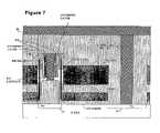
- FIG. 7is a cross sectional view along axis AA′ of FIG. 6 .
- the release plateincludes an insulating, semiconducting, or conducting layer;
- FIG. 8is a cross sectional view along axis BB′ of FIG. 6 ;
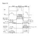
- FIG. 9is a schematic for an 8-bit array NRAM array based on the cell layout of FIG. 6 ;
- FIG. 10illustrates the operating voltages of the array of FIG. 9 in a block release mode
- FIG. 11illustrates voltages of the array of FIG. 9 in single bit or nibble release modes.
- Preferred embodiments of the inventionprovide a four terminal non-volatile transistor device. These embodiments, in essence, integrate a nanotube (NT) structure (such as a nanofabric article or ribbon) with a FET transistor. In preferred cases, the NT is integrated in such a way that external transistor connections are made only to the FET transistor terminals for deflecting the NT element into contact with the control gate, and the NT is switched internal to the device. The release gate is accessed directly. However, there is no direct contact to the NT element itself.
- NT-FETnanotube-FET
- the single transistor NT-FETcan be used in many applications, for example, an NRAM memory array of very small cell size. When used in such a non-volatile memory array, preferred layout designs occupy less than 8 F 2 cell area with bit selectivity for read, release, and write operations. There are many other applications because the NT-FET transistor is such a versatile active electrical element.
- NT-FET devices in product chipscan be used to repeatedly change on-chip generated timings and voltages after fabrication at the wafer level, or after chip assembly at the module, card, or system level. This can be done at the factory, or remotely in field locations. Such usage can enhance product yield, lower power, improve performance, and enhance reliability in a wide variety of products.
- a preferred NT-FET devicehas four terminals as shown in FIGS. 1 a–b : a control gate (CG), source (S), drain (D), and a reset gate (RG).
- CGcontrol gate
- Ssource
- Ddrain
- RGreset gate
- a floating gate (FG) and nanotube (NT) structureare combined to form a single floating gate nanotube (FGNT) element.
- the FGNTinteracts with control gate (CG), release gate (RG) and the FET channel as described below.
- FIG. 1 aillustrates the NT-FET in an OFF state in which the FGNT is electrically isolated from the terminals. This state is non-volatile.
- FIG. 1 billustrates the NT-FET in an ON state in which the FGNT is electrically connected to control gate CG. This state is also non-volatile.
- Preferred embodimentsinclude NFET and PFET CMOS devices, particularly NFET array devices in combination with nanotube electromechanical (NT) switch elements to provide unit cells that may be employed in integrated circuits.
- the nanotube electromechanical switch elementsare formed from matted, porous fabrics of nanotubes as described below.
- the NTis attached mechanically and electrically to a polysilicon floating gate to form the FGNT element that, in combination with CG, controls the channel of the NT-FET between the source (S) and drain (D) terminals.
- Switching the FGNT from the OFF state to the ON stateis controlled by applying appropriate voltages VNT SELECT between CG and FGNT.
- Switching from the ON state to the OFF stateis controlled by the difference in voltage VNT RELEASE between the release gate RG and floating gate nanotube element FGNT.
- Typical read and write operating voltages for the NT-FET deviceis in the range of 1 to 2.5 volts. Release operations require a higher voltage.
- the NT carbon fabricis suspended between control gate CG and release gate RG. As shown in FIGS. 2 a–b , the suspended NT fabric may be suspended horizontally or vertically. Typical suspended NT lengths are in the 90–180 nm range with gaps in the 5–30 nm range, for example.
- the NT-FET device operationrequires modulation of the channel region between the drain D and source S to make the channel conductive or not. This modulation is affected by a combination of voltages applied to control gate CG, drain D, and capacitive coupling effects.
- the capacitive couplingis between control gate CG, floating gate nanotube element FGNT, and the channel region (analogous to that in EPROM, EEPROM, and Flash EEPROM device structures).
- FIG. 3illustrates key capacitance coupling in the NT-FET device structure.
- the capacitance values C 12 , C 23 , C 27 and C 36are a function of material properties, film thicknesses, and the layout area (design) of the capacitor plates.
- Capacitance C 12is the capacitance between like numeral identified elements; e.g., control gate 1 and floating gate nanotube element 2 .
- capacitance C 36is a voltage-dependent capacitance modulated by drain voltage Vd.
- FIG. 3illustrates key capacitance coupling between elements of the NT-FET device structure.
- FIG. 3 aillustrates a device schematic with elements numbered to correspond to coupling capacitances.
- FIG. 3 billustrates a simplified cross section of the physical location of key coupling capacitors.
- Capacitance C 27is much smaller than capacitors C 12 and C 23 (by design), and its effect is ignored for these calculations.
- FIG. 4focuses on the channel region below gate FGNT.
- Sufficient voltage to the control gate V CGhas been applied such that the voltage on the floating gate nanotube element V FGNT exceeds the threshold voltage V TH to invert the channel region to make it conductive between drain and source.
- the source voltage Vsin this case floats (not forced). If the drain voltage Vd equals 0, then the inverted channel is at zero voltage, and voltage dependent capacitance C 36 is not part of the capacitance ratio controlling V FGNT as illustrated in FIG. 4 a .
- FGNTis relatively tightly coupled to the inverted channel. If, on the other hand, the drain voltage is positive, electrons flow from the channel region and the channel is depleted.
- FGNT to channel capacitance C 23is now in series with voltage modulated depletion capacitor C 36 as illustrated in FIG. 4 b . Since C 36 is typically 1 ⁇ 5 the value of C 23 for this type of structure, FGNT is decoupled from the FET channel region.
- FIG. 5illustrates the operations for switching of the NT-FET transistor to write a 0 or 1.
- the select voltageis applied between the control gate CG and floating gate nanotube element FGNT.
- the voltage levels internal to the NT-FET deviceare a function of the external applied voltages and the capacitor ratios internal to the NT-FET device.
- the representative voltageswere calculated using relative capacitance values. In this case, C 12 equals C 23 , and the value for C 36 is 1 ⁇ 5 of C 23 .
- FIG. 5 aillustrates the conditions for maximizing select voltage V NT SELECT for NT switching (ohmic-like contact with CG).
- FIG. 5 billustrates the conditions to minimize the V NT SELECT voltage so that NT is unchanged and remains in the OFF state.
- an NT structure with a select voltage threshold above 0.4 volts but less than 1.25 voltsmay be used for a switching (write) operation.
- Detecting or reading the ON or OFF state of the deviceis as follows. If the NT-FET device is in the ON state, CG is electrically connected to the floating gate nanotube element FGNT. For an FET device threshold of 0.7 volts, for example, V CG equals V FGNT which equals 1 volt. This forms a conductive channel between source and drain. If, however, the NT-FET device is in the OFF state, then for a control voltage V CG equals 1 volt and C 12 equals C 23 , the FET gate voltage V FGNT equals 0.5 volts and no channel is formed between source and drain.
- V CG ⁇ V FGNT0.5 volts
- the select threshold voltage rangeneeds to be above 0.5 volts but less than 1.25 volts to prevent an unwanted OFF to ON write transition during the read operation.
- Release operationsuse a voltage applied between release gate RG and floating gate nanotube element FGNT. Release voltages will range in the 2.1 to 6.5 volt range, depending on block versus bit level release considerations, as described below.
- FIG. 5illustrates the write mechanism based on applied voltages and relative capacitance values. The NT select voltage range shown was calculated for the write operation.
- FIG. 5 aillustrates conditions to switch the NT-FET device from the OFF to ON (write “1”) state.
- FIG. 5 billustrates conditions to maintain the NT-FET device in the OFF state.
- the NT-FET devicemay be used for very dense NRAM memory array as illustrated in top view in FIG. 6 .
- a cell boundaryis shown and labeled CELL.
- the word line WLforms the control gate CG.
- the release line RLcontacts RG.
- Array symmetryallows RG gate sharing between two adjacent cells.
- Array lines RL and RGare orthogonal to enable a single bit release option.
- the NTsare mounted in the vertical direction.
- the source diffusionis continuous between cells. Drain diffusions are shared between two adjacent cells and are contacted by a bit line BL.
- the BLs and WLsare ideally orthogonal.
- FIG. 7is a cross-sectional view of a cell taken along line AA′.
- the nanotube elements NTare suspended vertically, as suggested in FIG. 2 b , and illustrated in a vertical and un-deflected position.
- ON state(store a “1”)
- OFF state(store a “0”)
- nanotube element NTis in contact with RG the insulating, semiconducting, or metallic material covering layer.
- FIG. 8is a cross-sectional view of a cell taken along line BB′.
- FIG. 9is a schematic for an 8-bit array NRAM array based on the cell layout of FIG. 6 .
- the arrayis composed of eight non-volatile memory (storage) cells labeled 0 to 7 using the integrated NT-FET device.
- the memory arrayincludes word, bit, and release lines that are selected by decoders (not shown), and sense amplifiers (not shown) to detect the state (ON or OFF) of the array cells.
- the array of FIG. 9may be a sub-array of a much larger memory. Typical operating voltages are applied to the array using word lines, bit lines, and release lines. The resulting internal cell voltages are calculated as described in connection with the descriptions of FIGS. 3 , 4 , and 5 .
- the block moderesults in the simultaneous release of all NT-FETs in all eight array cells.
- the nibble release modefour of the eight NT-FETs in the eight array cells are simultaneously released.
- single bit releaseonly one NT-FET is released out of the eight cells in the array.
- the block release modeis the simplest and results in the broadest range of NT release voltages.
- the other release modesare more restrictive because some of the array cells of FIG. 9 are not released, and this requirement introduces additional electrical constraints.
- FIG. 10shows the operating voltages of the array of FIG. 9 applied to Cell 0 .
- Cell 0 operationis the same as that of all array cells (cells 0 – 7 ).
- a block release modeis employed such that cells 0 – 7 are all simultaneously released.
- individual cellsPrior to release, individual cells may be in the ON or OFF state. During the release time interval, if Cell 0 is in the ON state, then Cell 0 switches to the OFF state. If, however, Cell 0 is in the OFF state, then Cell 0 remains in the OFF state.
- the externally applied voltages to the terminals of device NT-FET 0 in array Cell 0are WL 0 driving CG 0 , RL 0 driving RG 0 , BL 0 driving drain diffusion D 0 , and the voltage applied to the shared source S 0 (not shown). These externally applied voltages couple to the internal nodes of device NT-FET 0 , as explained in connection with the description of FIGS. 3 , 4 , 5 , and result in the internal voltage applied to FGNT 0 .
- the combination of external and internal voltagesresults in the V NT RELEASE and V NT SELECT used to activate nanotube NT 0 during release and write operations.
- a release voltage of 6.5 voltswas chosen. However, 10 volts may be applied, for example, without affecting the array devices. The maximum voltage that can be applied is limited by the RL 0 peripheral driver considerations because RG 0 to FGNT 0 capacitance C 27 is small. If the array device prior to release is in the ON state, then word line WL 0 is electrically connected to FGNT 0 , and FGNT 0 is held at ground by WLO.
- the release voltagemay be sufficiently high to cause NT to deflect into contact with, or into close proximity to, the insulating layer on RG, with NT held in the “OFF” state by van der Waals forces.
- the release threshold of NT 0 for this exampleis V NT REL TH ⁇ 6.5 volts.
- V NT RELEASEcan reach ⁇ 2.1 volts.
- the release threshold voltage requirementis
- the write operationis preceded by a release operation so that device NT-FET 0 of Cell 0 is in the OFF state.
- the bit line BL 0 voltage Vdequals 0.
- the FGNT 0 voltage transitionis controlled by capacitance coupling and reaches 1.25 volts as WL 0 voltage transitions to 2.5 volts as illustrated in FIG. 5 . Therefore, the NT 0 select voltage V NT SELECT equals 1.25 volts as shown in FIG. 10 .
- device NT-FET 0switches to the ON state.
- Vdis held in the 1 to 2.5 volt range.
- FGNT 0transitions to 2.1 volts as illustrated in FIG. 5 . Therefore, the NT 0 select voltage is limited to V NT SELECT equals 0.4 volts.
- V NT SELECTselect threshold V NT SELECT
- device NT-FET 0remains in the OFF condition.
- the NT 0 structure threshold voltage requirement during write modeis V NT SEL TH greater than 0.4 volts and less than 1.25 volts.
- the source voltage Vs(not shown) is left in open (not used) during the write operation.
- BL 0is selected by the peripheral bit decoder/driver (not shown), set high and released at Vd equal to 1 volt.
- the common sourceis held at Vs equal to 0 volts.
- WL 0transitions to 1 volt. If NT-FET 0 is in the ON state, then FGNT 0 transitions to 1 volt since FGNT 0 is electrically connected. If the FET threshold voltage V TH of device NT-FET 0 is 0.7 volts, then the channel region is inverted and bit line BL 0 is discharged.
- word line WL 0 voltageis capacitively coupled to FGNT 0 , with FGNT 0 switching to 0.5 volts.
- V THan FET threshold voltage
- the FET channel of device NT-FET 0remains off, and the BL 0 is not discharged.
- the read and write waveforms of FIG. 10are unchanged. However, the release waveforms are changed as shown in FIG. 11 . If Cell 0 is to be released, then RL 0 is switched to 6.5 V with WL 0 at 0 volts as previously discussed. However, if another cell such as Cell 1 NT-FET 1 is to be released, without disturbing the state of NT-FET 0 in Cell 0 , then the WL 0 voltage must be increased to reduce the release voltage V NT RELEASE to a value below the release threshold voltage V NT REL TH . This in turn increases the voltage on gate FGNT 0 .
- the source and drain voltages of device NT-FET 0are held at the same voltage so no current flows in the FET channel during the release mode.
- the voltage applied to WL 0 (CG 0 )is limited by the voltage across the gate oxide of NT-FET 0 , especially in the ON state, when FGNT 0 and CG 0 are electrically connected. Assuming a gate oxide voltage limit of 3.5 volts, then the WL 0 voltage limit is 3.5 volts. To prevent the RL 0 voltage of 6.5 volts from releasing NT 0 of device NT-FET 0 , WL 0 is switched to 3.5 volts. The release voltage V NT RELEASE in Cell 0 is reduced to 3.0 volts.
- V NT REL TH voltage of NT 0is greater than 3.0 volts
- NT-FET 0remains unchanged.
- V NT REL THis greater than 3 volts and less than 6.5 volts becomes the release voltage range for the single bit release mode of operation.
- Nibble(4 bit, 1 ⁇ 2 byte release) allows half the array to be released simultaneously. Since not all bits are released simultaneously, the same release voltage range of V NT REL TH greater than 3.0 volts and less than 6.5 volts is used as in the single bit release mode.
- a NT element and an FET deviceare effectively integrated into a single non-volatile device referred to as a NT-FET device.
- the external read and write voltagesare low, in the 1 to 2.5 volt range, and the device operates at low voltage and current values.
- the release voltageis at least 6.5 volts, but has minimal effect on the internal NT-FET capacitance coupled voltages, because the release gate RG to FGNT capacitance C 27 is very small as a consequence of the array structure/layout.
- Layout of an NRAM cell based on the NT-FET devicecan produce a cell of less than 8 F 2 size. This cell can support single bit access for read, write, and release modes.
- Table 1provides a summary of the operating modes and voltage conditions for a preferred NT-FET device for assumed relative capacitance values. Changing assumed capacitance ratios and applied voltages changes the select and release conditions of the NT-FET device. These values are CG to FGNT capacitance C 12 equals C 23 , the FGNT to FET channel capacitance. Depletion layer capacitance C 36 equals 0.2 C 23 . The much smaller release gate RG to FGNT capacitance C 27 is less than 0.1 C 12 , and C 23 , and has minimal impact on the internal NT-FET voltage levels resulting from capacitance coupling. These capacitances are illustrated in FIG. 3 .
- the nanotube element of preferred devicesmay be constructed as explained in the following U.S. patents and/or applications, all of which are incorporated by reference in their entirety.
- Preferred nanotube elementsare made from a porous fabric of nanotubes.
- the fabricis highly porous and is substantially a monolayer of single-walled carbon nanotubes. See, e.g., U.S. Pat. Nos. 6,574,130, 6,643,165, and 6,706,402; See also U.S. Patent Publication Nos. 2003-0021966, 2003-0124325, 2003-0124837, and 2003-199172; and U.S. patent application Ser. Nos. 10/341,005, 10/341,054, 10/341,055, 10/341,130, 10/776,059, and 10/776,572.
- the technique chosenmust result in a sufficient quantity of nanotubes in contact with other nanotubes which thereby matte as a result of the nanotubes' adhesion characteristics.
- Certain embodimentse.g., memory cells
- the nanofabricis very thin (e.g., less than 2 nm); for example, when the nanofabric is primarily a monolayer of nanotubes with sporadic overlapping (sometimes fabric will have portions that are bilayers or trilayers), or a multilayer fabric with relatively small diameter nanotubes.
- SWNTssingle-walled nanotubes
- Other embodimentse.g., conductive traces
- MWNTsmulti-walled nanotubes
- the nanofabricis patterned using photolithographic techniques generating an electrically conductive trace of nanotubes, NT.
- inventionsmay employ double-walled nanotubes, including such nanotubes with metallic properties.
- the preferred embodimentuses electrostatic attractive forces to deflect the nanotube element, but other embodiments may use repulsive forces.
Landscapes
- Engineering & Computer Science (AREA)
- Microelectronics & Electronic Packaging (AREA)
- Chemical & Material Sciences (AREA)
- Nanotechnology (AREA)
- Physics & Mathematics (AREA)
- Mathematical Physics (AREA)
- Theoretical Computer Science (AREA)
- Crystallography & Structural Chemistry (AREA)
- Semiconductor Memories (AREA)
Abstract
Description
- U.S. Provisional Apl. Ser. No. 60/459,223 filed on Mar. 28, 2003, entitled NRAM Bit Selectable Two-Device Nanotube Array; and U.S. patent application Ser. No. (inserted upon USPTO designation), filed on the same day as the present application, entitled NRAM Bit Selectable Two-Device Nanotube Array.
- U.S. Provisional Apl. Ser. No. 60/459,222 filed on Mar. 28, 2003, entitled NRAM Byte/Block Released Bit Selectable One-Device Nanotube Array; and U.S. patent application Ser. No. (inserted upon USPTO designation), filed on the same day as the present application, entitled Non-Volatile Ram Cell and Array Using Nanotube Switch Position for Information State.
- U.S. Provisional Patent Application No. 60/459,224, filed on Mar. 28, 2003, entitled Nanotube-on-Gate FET Structures and Applications; and U.S. patent application Ser. No. (inserted upon USPTO designation), filed on the same day as the present application, entitled Nanotube-on-Gate FET Structures and Applications.
| MODE/ | |||||||
| CONDITION | VCG | Vd | Vs | VFGNT* | VNT SELECT+ | VRG | VNT RELEASE++ |
| READ | |||||||
| ON | 1.0 | 1.0 | 0 | 1.0 | 0 | 0 | −1.0 |
| OFF | 1.0 | 1.0 | 0 | 0.5 | 0.5 | 0 | −0.5 |
| WRITE “1” | 2.5 | 0 | float | 1.25 | 1.25 | 0 | −1.25 |
| OFF -> ON | |||||||
| WRITE “0” | 2.5 | 1–2.5 | float | 2.1 | 0.4 | 0 | −2.1 |
| OFF -> OFF | |||||||
| BLOCK REL | |||||||
| 0 | any | any | 0 | 0 | 6.5 | |2.1| < & < 6.5 | |
| ON/OFF | |||||||
| BIT/ | 0 | any | any | 0 | 0 | 6.5 | |2.1| < & < 6.5 |
| RELEASE | |||||||
| ON/OFF | |||||||
| NO RELEASE | |||||||
| ON | 3.5 | 1–2.5 | float | 3.5 | 0 | 6.5 | 3 < & < 6.5 |
| OFF | 3.5 | 1–2.5 | float | 3.0 | 0.5 | 6.5 | 3 < & < 6.5 |
| *FET VTH= 0.7 volts | Vd droops if NT-FET device is ON; |
| Vd unchanged if NT-FET device is OFF |
| +VNT SELECT= VCG− VFGNT | Requirement | 0.5 < VNT SEL TH< 1.25 volts |
| ++VNT RELEASE= VRG− VFGNT | Requirements | |
| Block Release: | |2.1| < VNT REL TH< 6.5** volts | |
| Bit/Nibble Release: | 3.5 < VNT REL TH< 6.5 volts |
| **Note: |
| limited by RL driver; can go to 10 volts |
Claims (19)
Priority Applications (1)
| Application Number | Priority Date | Filing Date | Title |
|---|---|---|---|
| US10/811,191US7075141B2 (en) | 2003-03-28 | 2004-03-26 | Four terminal non-volatile transistor device |
Applications Claiming Priority (2)
| Application Number | Priority Date | Filing Date | Title |
|---|---|---|---|
| US45925303P | 2003-03-28 | 2003-03-28 | |
| US10/811,191US7075141B2 (en) | 2003-03-28 | 2004-03-26 | Four terminal non-volatile transistor device |
Publications (2)
| Publication Number | Publication Date |
|---|---|
| US20050047244A1 US20050047244A1 (en) | 2005-03-03 |
| US7075141B2true US7075141B2 (en) | 2006-07-11 |
Family
ID=34221179
Family Applications (1)
| Application Number | Title | Priority Date | Filing Date |
|---|---|---|---|
| US10/811,191Expired - LifetimeUS7075141B2 (en) | 2003-03-28 | 2004-03-26 | Four terminal non-volatile transistor device |
Country Status (1)
| Country | Link |
|---|---|
| US (1) | US7075141B2 (en) |
Cited By (21)
| Publication number | Priority date | Publication date | Assignee | Title |
|---|---|---|---|---|
| WO2004088719A2 (en) | 2003-03-28 | 2004-10-14 | Nantero, Inc. | Nanotube-on-gate fet structures and applications |
| US20040238907A1 (en)* | 2003-06-02 | 2004-12-02 | Pinkerton Joseph F. | Nanoelectromechanical transistors and switch systems |
| US20060146594A1 (en)* | 2004-08-27 | 2006-07-06 | Micron Technology, Inc. | Integrated DRAM-NVRAM multi-level memory |
| US20060250856A1 (en)* | 2005-05-09 | 2006-11-09 | Nantero, Inc. | Memory arrays using nanotube articles with reprogrammable resistance |
| US20060250843A1 (en)* | 2005-05-09 | 2006-11-09 | Nantero, Inc. | Non-volatile-shadow latch using a nanotube switch |
| US20070018537A1 (en)* | 2003-06-02 | 2007-01-25 | Ambient Systems, Inc. | Energy conversion systems utilizing parallel array of automatic switches and generators |
| US20070048160A1 (en)* | 2005-07-19 | 2007-03-01 | Pinkerton Joseph F | Heat activated nanometer-scale pump |
| US20070133266A1 (en)* | 2005-12-01 | 2007-06-14 | Toshiharu Furukawa | Memory devices using carbon nanotube (cnt) technologies |
| US20070138888A1 (en)* | 2003-06-02 | 2007-06-21 | Pinkerton Joseph F | Electrical assemblies using molecular-scale electrically conductive and mechanically flexible beams and methods for application of same |
| US20070177418A1 (en)* | 2003-06-02 | 2007-08-02 | Ambient Systems, Inc. | Nanoelectromechanical memory cells and data storage devices |
| US20080079027A1 (en)* | 2004-06-09 | 2008-04-03 | Nantero, Inc. | Field effect devices having a gate controlled via a nanotube switching element |
| US20080099753A1 (en)* | 2006-10-31 | 2008-05-01 | Samsung Electronics Co., Ltd. | Phase change memory devices having dual lower electrodes and methods of fabricating the same |
| US20080233744A1 (en)* | 2005-09-19 | 2008-09-25 | California Institute Of Technology | Carbon nanotube switches for memory, rf communications and sensing applications, and methods of making the same |
| US20080251865A1 (en)* | 2007-04-03 | 2008-10-16 | Pinkerton Joseph F | Nanoelectromechanical systems and methods for making the same |
| US7518283B2 (en) | 2004-07-19 | 2009-04-14 | Cjp Ip Holdings Ltd. | Nanometer-scale electrostatic and electromagnetic motors and generators |
| US20090303337A1 (en)* | 2003-07-18 | 2009-12-10 | Katsumi Kaneko | Image pick-up device and synchronization-signal-generating device |
| US7781862B2 (en) | 2005-05-09 | 2010-08-24 | Nantero, Inc. | Two-terminal nanotube devices and systems and methods of making same |
| US20110056812A1 (en)* | 2009-09-08 | 2011-03-10 | Kaul Anupama B | Nano-electro-mechanical switches using three-dimensional sidewall-conductive carbon nanofibers and method for making the same |
| US7986546B2 (en) | 2005-05-09 | 2011-07-26 | Nantero, Inc. | Non-volatile shadow latch using a nanotube switch |
| US20110212535A1 (en)* | 2010-01-13 | 2011-09-01 | Kaul Anupama B | Applications and methods of operating a three-dimensional nano-electro-mechanical resonator and related devices |
| US8699268B2 (en) | 2003-06-09 | 2014-04-15 | Nantero Inc. | Field effect devices controlled via a nanotube switching element |
Families Citing this family (35)
| Publication number | Priority date | Publication date | Assignee | Title |
|---|---|---|---|---|
| US6835591B2 (en)* | 2001-07-25 | 2004-12-28 | Nantero, Inc. | Methods of nanotube films and articles |
| US6574130B2 (en) | 2001-07-25 | 2003-06-03 | Nantero, Inc. | Hybrid circuit having nanotube electromechanical memory |
| US7259410B2 (en)* | 2001-07-25 | 2007-08-21 | Nantero, Inc. | Devices having horizontally-disposed nanofabric articles and methods of making the same |
| US6924538B2 (en)* | 2001-07-25 | 2005-08-02 | Nantero, Inc. | Devices having vertically-disposed nanofabric articles and methods of making the same |
| US6706402B2 (en)* | 2001-07-25 | 2004-03-16 | Nantero, Inc. | Nanotube films and articles |
| US7335395B2 (en)* | 2002-04-23 | 2008-02-26 | Nantero, Inc. | Methods of using pre-formed nanotubes to make carbon nanotube films, layers, fabrics, ribbons, elements and articles |
| US7858185B2 (en)* | 2003-09-08 | 2010-12-28 | Nantero, Inc. | High purity nanotube fabrics and films |
| US7560136B2 (en)* | 2003-01-13 | 2009-07-14 | Nantero, Inc. | Methods of using thin metal layers to make carbon nanotube films, layers, fabrics, ribbons, elements and articles |
| US6944054B2 (en)* | 2003-03-28 | 2005-09-13 | Nantero, Inc. | NRAM bit selectable two-device nanotube array |
| US7294877B2 (en)* | 2003-03-28 | 2007-11-13 | Nantero, Inc. | Nanotube-on-gate FET structures and applications |
| US7113426B2 (en)* | 2003-03-28 | 2006-09-26 | Nantero, Inc. | Non-volatile RAM cell and array using nanotube switch position for information state |
| US7045421B2 (en)* | 2003-04-22 | 2006-05-16 | Nantero, Inc. | Process for making bit selectable devices having elements made with nanotubes |
| CA2526946A1 (en)* | 2003-05-14 | 2005-04-07 | Nantero, Inc. | Sensor platform using a non-horizontally oriented nanotube element |
| US7274064B2 (en)* | 2003-06-09 | 2007-09-25 | Nanatero, Inc. | Non-volatile electromechanical field effect devices and circuits using same and methods of forming same |
| EP1665278A4 (en)* | 2003-08-13 | 2007-11-07 | Nantero Inc | NANOTUBE SWITCHING ELEMENTS COMPRISING MULTIPLE CONTROLS AND CIRCUITS PRODUCED FROM THESE ELEMENTS |
| US7289357B2 (en) | 2003-08-13 | 2007-10-30 | Nantero, Inc. | Isolation structure for deflectable nanotube elements |
| US7375369B2 (en)* | 2003-09-08 | 2008-05-20 | Nantero, Inc. | Spin-coatable liquid for formation of high purity nanotube films |
| US7504051B2 (en)* | 2003-09-08 | 2009-03-17 | Nantero, Inc. | Applicator liquid for use in electronic manufacturing processes |
| US7528437B2 (en) | 2004-02-11 | 2009-05-05 | Nantero, Inc. | EEPROMS using carbon nanotubes for cell storage |
| US7658869B2 (en)* | 2004-06-03 | 2010-02-09 | Nantero, Inc. | Applicator liquid containing ethyl lactate for preparation of nanotube films |
| US7556746B2 (en)* | 2004-06-03 | 2009-07-07 | Nantero, Inc. | Method of making an applicator liquid for electronics fabrication process |
| US7167026B2 (en)* | 2004-06-18 | 2007-01-23 | Nantero, Inc. | Tri-state circuit using nanotube switching elements |
| US7652342B2 (en) | 2004-06-18 | 2010-01-26 | Nantero, Inc. | Nanotube-based transfer devices and related circuits |
| US7288970B2 (en)* | 2004-06-18 | 2007-10-30 | Nantero, Inc. | Integrated nanotube and field effect switching device |
| TWI399864B (en)* | 2004-09-16 | 2013-06-21 | Nantero Inc | Light emitters using nanotubes and methods of making same |
| EP1825038B1 (en) | 2004-12-16 | 2012-09-12 | Nantero, Inc. | Aqueous carbon nanotube applicator liquids and methods for producing applicator liquids thereof |
| US20060220094A1 (en)* | 2005-03-31 | 2006-10-05 | Bohumil Lojek | Non-volatile memory transistor with nanotube floating gate |
| US7598127B2 (en)* | 2005-05-12 | 2009-10-06 | Nantero, Inc. | Nanotube fuse structure |
| US7575693B2 (en)* | 2005-05-23 | 2009-08-18 | Nantero, Inc. | Method of aligning nanotubes and wires with an etched feature |
| US7541216B2 (en)* | 2005-06-09 | 2009-06-02 | Nantero, Inc. | Method of aligning deposited nanotubes onto an etched feature using a spacer |
| US7402770B2 (en)* | 2005-06-10 | 2008-07-22 | Lsi Logic Corporation | Nano structure electrode design |
| US7538040B2 (en) | 2005-06-30 | 2009-05-26 | Nantero, Inc. | Techniques for precision pattern transfer of carbon nanotubes from photo mask to wafers |
| US20070031318A1 (en)* | 2005-08-03 | 2007-02-08 | Jie Liu | Methods of chemically treating an electrically conductive layer having nanotubes therein with diazonium reagent |
| GB0611557D0 (en)* | 2006-06-12 | 2006-07-19 | Univ Belfast | Nanostructured systems and a method of manufacture of the same |
| US8698226B2 (en)* | 2008-07-31 | 2014-04-15 | University Of Connecticut | Semiconductor devices, methods of manufacture thereof and articles comprising the same |
Citations (44)
| Publication number | Priority date | Publication date | Assignee | Title |
|---|---|---|---|---|
| US3448302A (en) | 1966-06-16 | 1969-06-03 | Itt | Operating circuit for phase change memory devices |
| US4845533A (en) | 1986-08-22 | 1989-07-04 | Energy Conversion Devices, Inc. | Thin film electrical devices with amorphous carbon electrodes and method of making same |
| US4853893A (en) | 1987-07-02 | 1989-08-01 | Ramtron Corporation | Data storage device and method of using a ferroelectric capacitance divider |
| US4876667A (en) | 1987-06-22 | 1989-10-24 | Energy Conversion Devices, Inc. | Data storage device having a phase change memory medium reversible by direct overwrite |
| US4888630A (en) | 1988-03-21 | 1989-12-19 | Texas Instruments Incorporated | Floating-gate transistor with a non-linear intergate dielectric |
| US5198994A (en) | 1988-08-31 | 1993-03-30 | Kabushiki Kaisha Toshiba | Ferroelectric memory device |
| US6044008A (en) | 1997-06-20 | 2000-03-28 | Hyundai Electronics Industries Co., Ltd. | Ferroelectric RAM device |
| US6128214A (en) | 1999-03-29 | 2000-10-03 | Hewlett-Packard | Molecular wire crossbar memory |
| US6159620A (en) | 1997-03-31 | 2000-12-12 | The Regents Of The University Of California | Single-electron solid state electronic device |
| WO2001003208A1 (en) | 1999-07-02 | 2001-01-11 | President And Fellows Of Harvard College | Nanoscopic wire-based devices, arrays, and methods of their manufacture |
| US6183714B1 (en) | 1995-09-08 | 2001-02-06 | Rice University | Method of making ropes of single-wall carbon nanotubes |
| US6198655B1 (en) | 1999-12-10 | 2001-03-06 | The Regents Of The University Of California | Electrically addressable volatile non-volatile molecular-based switching devices |
| US6221330B1 (en) | 1997-08-04 | 2001-04-24 | Hyperion Catalysis International Inc. | Process for producing single wall nanotubes using unsupported metal catalysts |
| US6232706B1 (en) | 1998-11-12 | 2001-05-15 | The Board Of Trustees Of The Leland Stanford Junior University | Self-oriented bundles of carbon nanotubes and method of making same |
| WO2001044796A1 (en) | 1999-12-15 | 2001-06-21 | Board Of Trustees Of The Leland Stanford Junior University | Carbon nanotube devices |
| US6445006B1 (en) | 1995-12-20 | 2002-09-03 | Advanced Technology Materials, Inc. | Microelectronic and microelectromechanical devices comprising carbon nanotube components, and methods of making same |
| US20020130311A1 (en) | 2000-08-22 | 2002-09-19 | Lieber Charles M. | Doped elongated semiconductors, growing such semiconductors, devices including such semiconductors and fabricating such devices |
| US20020172963A1 (en) | 2001-01-10 | 2002-11-21 | Kelley Shana O. | DNA-bridged carbon nanotube arrays |
| US20020179434A1 (en) | 1998-08-14 | 2002-12-05 | The Board Of Trustees Of The Leland Stanford Junior University | Carbon nanotube devices |
| US20030021966A1 (en) | 2001-07-25 | 2003-01-30 | Segal Brent M. | Electromechanical memory array using nanotube ribbons and method for making same |
| US6518156B1 (en) | 1999-03-29 | 2003-02-11 | Hewlett-Packard Company | Configurable nanoscale crossbar electronic circuits made by electrochemical reaction |
| US6548841B2 (en) | 2000-11-09 | 2003-04-15 | Texas Instruments Incorporated | Nanomechanical switches and circuits |
| US6559468B1 (en) | 1999-03-29 | 2003-05-06 | Hewlett-Packard Development Company Lp | Molecular wire transistor (MWT) |
| US6574130B2 (en) | 2001-07-25 | 2003-06-03 | Nantero, Inc. | Hybrid circuit having nanotube electromechanical memory |
| US20030124325A1 (en) | 2001-12-28 | 2003-07-03 | Thomas Rueckes | Electromechanical three-trace junction devices |
| US20030124837A1 (en) | 2001-12-28 | 2003-07-03 | Thomas Rueckes | Methods of making electromechanical three-trace junction devices |
| US20030199172A1 (en) | 2001-07-25 | 2003-10-23 | Thomas Rueckes | Methods of nanotube films and articles |
| US6643165B2 (en) | 2001-07-25 | 2003-11-04 | Nantero, Inc. | Electromechanical memory having cell selection circuitry constructed with nanotube technology |
| WO2003091486A1 (en) | 2002-04-23 | 2003-11-06 | Nantero, Inc. | Methods of using pre-formed nanotubes to make carbon nanotube films, layers, fabrics, ribbons, elements and articles |
| US20030236000A1 (en) | 2002-06-19 | 2003-12-25 | Nantero, Inc. | Method of making nanotube permeable base transistor |
| US20030234407A1 (en) | 2002-06-19 | 2003-12-25 | Nantero, Inc. | Nanotube permeable base transistor |
| US6673424B1 (en) | 2001-06-19 | 2004-01-06 | Arizona Board Of Regents | Devices based on molecular electronics |
| US6750471B2 (en) | 1998-11-18 | 2004-06-15 | International Business Machines Corporation | Molecular memory & logic |
| WO2004065671A1 (en) | 2003-01-13 | 2004-08-05 | Nantero, Inc. | Carbon nanotube films, layers, fabrics, ribbons, elements and articles |
| WO2004065655A1 (en) | 2003-01-13 | 2004-08-05 | Nantero, Inc. | Methods of using thin metal layers to make carbon nanotube films, layers, fabrics, ribbons, elements and articles |
| WO2004065657A1 (en) | 2003-01-13 | 2004-08-05 | Nantero, Inc. | Methods of making carbon nanotube films, layers, fabrics, ribbons, elements and articles |
| US20040164289A1 (en) | 2001-12-28 | 2004-08-26 | Nantero, Inc. | Electromechanical three-trace junction devices |
| US20040175856A1 (en) | 2001-07-25 | 2004-09-09 | Nantero, Inc. | Devices having vertically-disposed nanofabric articles and methods of marking the same |
| US20040181630A1 (en) | 2001-07-25 | 2004-09-16 | Nantero, Inc. | Devices having horizontally-disposed nanofabric articles and methods of making the same |
| US6803840B2 (en) | 2001-03-30 | 2004-10-12 | California Institute Of Technology | Pattern-aligned carbon nanotube growth and tunable resonator apparatus |
| US6809465B2 (en) | 2002-08-23 | 2004-10-26 | Samsung Electronics Co., Ltd. | Article comprising MEMS-based two-dimensional e-beam sources and method for making the same |
| US20050041465A1 (en) | 2003-03-28 | 2005-02-24 | Nantero, Inc. | Nram bit selectable two-device nanotube array |
| US20050041466A1 (en) | 2003-03-28 | 2005-02-24 | Nantero, Inc. | Non-volatile RAM cell and array using nanotube switch position for information state |
| US20050056877A1 (en) | 2003-03-28 | 2005-03-17 | Nantero, Inc. | Nanotube-on-gate fet structures and applications |
Family Cites Families (1)
| Publication number | Priority date | Publication date | Assignee | Title |
|---|---|---|---|---|
| DE19935998B4 (en)* | 1999-07-30 | 2007-10-18 | Osram Opto Semiconductors Gmbh | Multiple semiconductor laser structure with narrow wavelength distribution |
- 2004
- 2004-03-26USUS10/811,191patent/US7075141B2/ennot_activeExpired - Lifetime
Patent Citations (57)
| Publication number | Priority date | Publication date | Assignee | Title |
|---|---|---|---|---|
| US3448302A (en) | 1966-06-16 | 1969-06-03 | Itt | Operating circuit for phase change memory devices |
| US4845533A (en) | 1986-08-22 | 1989-07-04 | Energy Conversion Devices, Inc. | Thin film electrical devices with amorphous carbon electrodes and method of making same |
| US4876667A (en) | 1987-06-22 | 1989-10-24 | Energy Conversion Devices, Inc. | Data storage device having a phase change memory medium reversible by direct overwrite |
| US4853893A (en) | 1987-07-02 | 1989-08-01 | Ramtron Corporation | Data storage device and method of using a ferroelectric capacitance divider |
| US4888630A (en) | 1988-03-21 | 1989-12-19 | Texas Instruments Incorporated | Floating-gate transistor with a non-linear intergate dielectric |
| US5198994A (en) | 1988-08-31 | 1993-03-30 | Kabushiki Kaisha Toshiba | Ferroelectric memory device |
| US6183714B1 (en) | 1995-09-08 | 2001-02-06 | Rice University | Method of making ropes of single-wall carbon nanotubes |
| US6445006B1 (en) | 1995-12-20 | 2002-09-03 | Advanced Technology Materials, Inc. | Microelectronic and microelectromechanical devices comprising carbon nanotube components, and methods of making same |
| US6159620A (en) | 1997-03-31 | 2000-12-12 | The Regents Of The University Of California | Single-electron solid state electronic device |
| US6044008A (en) | 1997-06-20 | 2000-03-28 | Hyundai Electronics Industries Co., Ltd. | Ferroelectric RAM device |
| US6221330B1 (en) | 1997-08-04 | 2001-04-24 | Hyperion Catalysis International Inc. | Process for producing single wall nanotubes using unsupported metal catalysts |
| US20020179434A1 (en) | 1998-08-14 | 2002-12-05 | The Board Of Trustees Of The Leland Stanford Junior University | Carbon nanotube devices |
| US6232706B1 (en) | 1998-11-12 | 2001-05-15 | The Board Of Trustees Of The Leland Stanford Junior University | Self-oriented bundles of carbon nanotubes and method of making same |
| US6750471B2 (en) | 1998-11-18 | 2004-06-15 | International Business Machines Corporation | Molecular memory & logic |
| US6128214A (en) | 1999-03-29 | 2000-10-03 | Hewlett-Packard | Molecular wire crossbar memory |
| US6518156B1 (en) | 1999-03-29 | 2003-02-11 | Hewlett-Packard Company | Configurable nanoscale crossbar electronic circuits made by electrochemical reaction |
| US6559468B1 (en) | 1999-03-29 | 2003-05-06 | Hewlett-Packard Development Company Lp | Molecular wire transistor (MWT) |
| US20020130353A1 (en) | 1999-07-02 | 2002-09-19 | Lieber Charles M. | Nanoscopic wire-based devices, arrays, and methods of their manufacture |
| US6781166B2 (en) | 1999-07-02 | 2004-08-24 | President & Fellows Of Harvard College | Nanoscopic wire-based devices and arrays |
| WO2001003208A1 (en) | 1999-07-02 | 2001-01-11 | President And Fellows Of Harvard College | Nanoscopic wire-based devices, arrays, and methods of their manufacture |
| US6198655B1 (en) | 1999-12-10 | 2001-03-06 | The Regents Of The University Of California | Electrically addressable volatile non-volatile molecular-based switching devices |
| WO2001044796A1 (en) | 1999-12-15 | 2001-06-21 | Board Of Trustees Of The Leland Stanford Junior University | Carbon nanotube devices |
| US20020130311A1 (en) | 2000-08-22 | 2002-09-19 | Lieber Charles M. | Doped elongated semiconductors, growing such semiconductors, devices including such semiconductors and fabricating such devices |
| US6548841B2 (en) | 2000-11-09 | 2003-04-15 | Texas Instruments Incorporated | Nanomechanical switches and circuits |
| US20020172963A1 (en) | 2001-01-10 | 2002-11-21 | Kelley Shana O. | DNA-bridged carbon nanotube arrays |
| US6803840B2 (en) | 2001-03-30 | 2004-10-12 | California Institute Of Technology | Pattern-aligned carbon nanotube growth and tunable resonator apparatus |
| US6673424B1 (en) | 2001-06-19 | 2004-01-06 | Arizona Board Of Regents | Devices based on molecular electronics |
| US20030199172A1 (en) | 2001-07-25 | 2003-10-23 | Thomas Rueckes | Methods of nanotube films and articles |
| US20040159833A1 (en) | 2001-07-25 | 2004-08-19 | Nantero, Inc. | Nanotube films and articles |
| US6643165B2 (en) | 2001-07-25 | 2003-11-04 | Nantero, Inc. | Electromechanical memory having cell selection circuitry constructed with nanotube technology |
| US6919592B2 (en)* | 2001-07-25 | 2005-07-19 | Nantero, Inc. | Electromechanical memory array using nanotube ribbons and method for making same |
| US20040214366A1 (en) | 2001-07-25 | 2004-10-28 | Nantero, Inc. | Electromechanical memory array using nanotube ribbons and method for making same |
| US20040214367A1 (en) | 2001-07-25 | 2004-10-28 | Nantero, Inc. | Electromechanical memory array using nanotube ribbons and method for making same |
| US20030021966A1 (en) | 2001-07-25 | 2003-01-30 | Segal Brent M. | Electromechanical memory array using nanotube ribbons and method for making same |
| US6706402B2 (en) | 2001-07-25 | 2004-03-16 | Nantero, Inc. | Nanotube films and articles |
| US20040085805A1 (en) | 2001-07-25 | 2004-05-06 | Nantero, Inc. | Device selection circuitry constructed with nanotube technology |
| US20040181630A1 (en) | 2001-07-25 | 2004-09-16 | Nantero, Inc. | Devices having horizontally-disposed nanofabric articles and methods of making the same |
| US20040175856A1 (en) | 2001-07-25 | 2004-09-09 | Nantero, Inc. | Devices having vertically-disposed nanofabric articles and methods of marking the same |
| US6574130B2 (en) | 2001-07-25 | 2003-06-03 | Nantero, Inc. | Hybrid circuit having nanotube electromechanical memory |
| US20030165074A1 (en) | 2001-07-25 | 2003-09-04 | Nantero, Inc. | Hybrid circuit having nanotube electromechanical memory |
| US20040191978A1 (en) | 2001-12-28 | 2004-09-30 | Nantero, Inc. | Methods of making electromechanical three-trace junction devices |
| US20030124837A1 (en) | 2001-12-28 | 2003-07-03 | Thomas Rueckes | Methods of making electromechanical three-trace junction devices |
| US20030124325A1 (en) | 2001-12-28 | 2003-07-03 | Thomas Rueckes | Electromechanical three-trace junction devices |
| US6784028B2 (en) | 2001-12-28 | 2004-08-31 | Nantero, Inc. | Methods of making electromechanical three-trace junction devices |
| US20040164289A1 (en) | 2001-12-28 | 2004-08-26 | Nantero, Inc. | Electromechanical three-trace junction devices |
| WO2003091486A1 (en) | 2002-04-23 | 2003-11-06 | Nantero, Inc. | Methods of using pre-formed nanotubes to make carbon nanotube films, layers, fabrics, ribbons, elements and articles |
| US6759693B2 (en) | 2002-06-19 | 2004-07-06 | Nantero, Inc. | Nanotube permeable base transistor |
| US6774052B2 (en) | 2002-06-19 | 2004-08-10 | Nantero, Inc. | Method of making nanotube permeable base transistor |
| US20030234407A1 (en) | 2002-06-19 | 2003-12-25 | Nantero, Inc. | Nanotube permeable base transistor |
| US20030236000A1 (en) | 2002-06-19 | 2003-12-25 | Nantero, Inc. | Method of making nanotube permeable base transistor |
| US6809465B2 (en) | 2002-08-23 | 2004-10-26 | Samsung Electronics Co., Ltd. | Article comprising MEMS-based two-dimensional e-beam sources and method for making the same |
| WO2004065671A1 (en) | 2003-01-13 | 2004-08-05 | Nantero, Inc. | Carbon nanotube films, layers, fabrics, ribbons, elements and articles |
| WO2004065655A1 (en) | 2003-01-13 | 2004-08-05 | Nantero, Inc. | Methods of using thin metal layers to make carbon nanotube films, layers, fabrics, ribbons, elements and articles |
| WO2004065657A1 (en) | 2003-01-13 | 2004-08-05 | Nantero, Inc. | Methods of making carbon nanotube films, layers, fabrics, ribbons, elements and articles |
| US20050041465A1 (en) | 2003-03-28 | 2005-02-24 | Nantero, Inc. | Nram bit selectable two-device nanotube array |
| US20050041466A1 (en) | 2003-03-28 | 2005-02-24 | Nantero, Inc. | Non-volatile RAM cell and array using nanotube switch position for information state |
| US20050056877A1 (en) | 2003-03-28 | 2005-03-17 | Nantero, Inc. | Nanotube-on-gate fet structures and applications |
Non-Patent Citations (29)
| Title |
|---|
| Ajayan, P.M., et al., "Nanometre-size tubes of carbon," Rep. Prog. Phys., 1997. vol. 60, pp. 1025-1062. |
| Ami, S. et al., "Logic gates and memory cells based on single C<SUB>60 </SUB>electromechanical transistors," Nanotechnology, 2001, vol. 12, pp. 44-52. |
| Avouris, Ph., "Carbon nanotube electronics," Chem. Physics, 2002, vol. 281, pp. 429-445. |
| Casavant, M.J. et al., "Neat macroscopic membranes of aligned carbon nanotubes," Journal of Appl. Phys., 2003, vol. 93(4), pp. 2153-2156. |
| Choi, W.B. et al., "Carbon-nanotube-based nonvolatile memory with oxide-nitride-film and nanoscale channel," Appl. Phys. Lett., 2003, vol. 82(2), pp. 275-277. |
| Cui, J.B. et al., "Carbon Nanotube Memory Devices of High Charge Storage Stability," Appl. Phys. Lett., 2002, vol. 81(17), pp. 3260-3262. |
| Dai, H. et al., "Controlled Chemical Routes to nanotube Architectures, Physics, and Devices," J. Phys. Chem. B, 1999. vol. 103, pp. 111246-11255. |
| Dehon, A., "Array-Based Architecture for FET-Based, Nanoscale Electronics," IEEE Transactions on Nanotechnology, 2003, vol. 2(1), pp. 23-32. |
| Dequesnes, M. et al., "Calculation of pull-in voltages for carbon-nanotube-based nanoelectromechanical switches," Nanotechnology, 2002, vol. 13, pp. 120-131. |
| Dequesnes, M. et al., "Simulation of carbon nanotube-based nanoelectromechanical switches," Computational Nanoscience and Nanotechnology, 2002, pp. 383-386. |
| Fan, S. et al., "Carbon nanotube arrays on silicon substrates and their possible application," Physica E, 2000, vol. 8, pp. 179-183. |
| Farajian, A. A. et al., "Electronic transport through bent carbon nanotubes: Nanoelectromechanical sensors and switches," Phys. Rev. B, 2003, vol. 67, pp. 205423-1-205423-6. |
| Fischer, J.E. et al., "Magnetically aligned single wall carbon nanotube films: Preferred orientation and anisotropic transport properties," Journal of Appl. Phys., 2003, vol. 93(4), pp. 2157-2163. |
| Franklin, N. R. et al., "Integration of suspended carbon nanotube arrays into electronic devices and electromechanical systems," Appl. Phys. Lett., 2002,vol. 81(5), pp. 913-915. |
| Fuhrer, M.S. et al., "High-Mobility Nanotube Transistor Memory," Nano Letters, 2002, vol. 2(7), pp. 755-759. |
| Homma, Y. et al., "Growth of Suspended Carbon Nanotubes Networks on 100-nm-scale Silicon Pillars," Appl. Phys. Lett., 2002, vol. 81(12), pp. 2261-2263. |
| Kinaret, J.M. et al., "A carbon-nanotube-based nanorelay", Appl. Phys. Lett., 2003, vol. 82(8), pp. 1287-1289. |
| Lee, K.H. et al., "Control of growth orientation for carbon nanotubes," Appl. Phys. Lett., 2003, vol. 82(3), pp. 448-450. |
| Radosavljevic, M. et al., "Nonvolatile molecular memory elements based on ambipolar nanotube field effect transistors," Nano Letters, 2002, vol. 2(7), pp. 761-764. |
| Robinson, L.A.W., "Self-Aligned Electrodes for Suspended Carbon Nanotube Structures," Microelectronic Engineering, 2003, vol. 67-68, pp. 615-622. |
| Rueckes, T., et al., "Carbon Nanotube-Based Nonvolatile Random Access Memory for Molecular Computing" Science, 2000, vol. 289, pp. 94-97. |
| Soh, H. T. et al., "Integrated nanotube circuits: Controlled growth and ohmic contacting of single-walled carbon nanotubes," Appl. Phys. Lett., 1999. vol. 75(5), pp. 627-629. |
| Sreekumar, T.V., et al., "Single-wall Carbon Nanotube Films", Chem. Mater. 2003, vol. 15, pp. 175-178. |
| Tans, S. et al., "Room-temperature based on a single carbon nanotube," Nature, 1998. vol. 393, pp. 49-52. |
| Tour, J. M. et al., "NanoCell Electronic Memories," J. Am. Chem. Soc., 2003, vol. 125, ppl 13279-13283. |
| Verissimo-Alves, M. et al., "Electomechanical effects in carbon nanotubes: Ab initio and analytical tight-binding calculations," Phys. Rev. B, 2003, vol. 67, pp. 161401-1-161401-4. |
| Wolf, S., Multilevel-Interconnect Technology for VLSI and ULSI, 1990, Lattice Press, Sunset Beach, pp. 189-191. |
| Wolf, S., Silicon Processing for the VLSI Era; vol. II-Manufacturing Yield and Reliability Issues of VLSI Interconnects, 1991, Lattice Press, Sunset Beach, pp. 260-273. |
| Zhan, W. et al., "Microelectrochemical Logic Circuits," J. Am. Chem. Soc., 2003, vol. 125, pp. 9934-9935. |
Cited By (40)
| Publication number | Priority date | Publication date | Assignee | Title |
|---|---|---|---|---|
| WO2004088719A2 (en) | 2003-03-28 | 2004-10-14 | Nantero, Inc. | Nanotube-on-gate fet structures and applications |
| US20070138888A1 (en)* | 2003-06-02 | 2007-06-21 | Pinkerton Joseph F | Electrical assemblies using molecular-scale electrically conductive and mechanically flexible beams and methods for application of same |
| US20040238907A1 (en)* | 2003-06-02 | 2004-12-02 | Pinkerton Joseph F. | Nanoelectromechanical transistors and switch systems |
| US7495350B2 (en)* | 2003-06-02 | 2009-02-24 | Cjp Ip Holdings, Ltd. | Energy conversion systems utilizing parallel array of automatic switches and generators |
| US7582992B2 (en) | 2003-06-02 | 2009-09-01 | Cjp Ip Holdings, Ltd. | Electrical assemblies using molecular-scale electrically conductive and mechanically flexible beams and methods for application of same |
| US20070018537A1 (en)* | 2003-06-02 | 2007-01-25 | Ambient Systems, Inc. | Energy conversion systems utilizing parallel array of automatic switches and generators |
| US7362605B2 (en) | 2003-06-02 | 2008-04-22 | Ambient Systems, Inc. | Nanoelectromechanical memory cells and data storage devices |
| US20070177418A1 (en)* | 2003-06-02 | 2007-08-02 | Ambient Systems, Inc. | Nanoelectromechanical memory cells and data storage devices |
| US8699268B2 (en) | 2003-06-09 | 2014-04-15 | Nantero Inc. | Field effect devices controlled via a nanotube switching element |
| US20090303337A1 (en)* | 2003-07-18 | 2009-12-10 | Katsumi Kaneko | Image pick-up device and synchronization-signal-generating device |
| US20080079027A1 (en)* | 2004-06-09 | 2008-04-03 | Nantero, Inc. | Field effect devices having a gate controlled via a nanotube switching element |
| US7709880B2 (en)* | 2004-06-09 | 2010-05-04 | Nantero, Inc. | Field effect devices having a gate controlled via a nanotube switching element |
| US7518283B2 (en) | 2004-07-19 | 2009-04-14 | Cjp Ip Holdings Ltd. | Nanometer-scale electrostatic and electromagnetic motors and generators |
| US7379336B2 (en)* | 2004-08-27 | 2008-05-27 | Micron Technology, Inc. | Integrated DRAM-NVRAM multi-level memory |
| US20060146594A1 (en)* | 2004-08-27 | 2006-07-06 | Micron Technology, Inc. | Integrated DRAM-NVRAM multi-level memory |
| US7781862B2 (en) | 2005-05-09 | 2010-08-24 | Nantero, Inc. | Two-terminal nanotube devices and systems and methods of making same |
| US7394687B2 (en) | 2005-05-09 | 2008-07-01 | Nantero, Inc. | Non-volatile-shadow latch using a nanotube switch |
| US20060250856A1 (en)* | 2005-05-09 | 2006-11-09 | Nantero, Inc. | Memory arrays using nanotube articles with reprogrammable resistance |
| US7479654B2 (en) | 2005-05-09 | 2009-01-20 | Nantero, Inc. | Memory arrays using nanotube articles with reprogrammable resistance |
| US8580586B2 (en) | 2005-05-09 | 2013-11-12 | Nantero Inc. | Memory arrays using nanotube articles with reprogrammable resistance |
| US7986546B2 (en) | 2005-05-09 | 2011-07-26 | Nantero, Inc. | Non-volatile shadow latch using a nanotube switch |
| US20060250843A1 (en)* | 2005-05-09 | 2006-11-09 | Nantero, Inc. | Non-volatile-shadow latch using a nanotube switch |
| US20070048160A1 (en)* | 2005-07-19 | 2007-03-01 | Pinkerton Joseph F | Heat activated nanometer-scale pump |
| US20080233744A1 (en)* | 2005-09-19 | 2008-09-25 | California Institute Of Technology | Carbon nanotube switches for memory, rf communications and sensing applications, and methods of making the same |
| US7446044B2 (en) | 2005-09-19 | 2008-11-04 | California Institute Of Technology | Carbon nanotube switches for memory, RF communications and sensing applications, and methods of making the same |
| US7483285B2 (en) | 2005-12-01 | 2009-01-27 | International Business Machines Corporation | Memory devices using carbon nanotube (CNT) technologies |
| US20080117671A1 (en)* | 2005-12-01 | 2008-05-22 | Toshiharu Furukawa | Memory devices using carbon nanotube (cnt) technologies |
| US7385839B2 (en)* | 2005-12-01 | 2008-06-10 | International Business Machines Corporation | Memory devices using carbon nanotube (CNT) technologies |
| US20070133266A1 (en)* | 2005-12-01 | 2007-06-14 | Toshiharu Furukawa | Memory devices using carbon nanotube (cnt) technologies |
| US8129214B2 (en) | 2006-10-31 | 2012-03-06 | Samsung Electronics Co., Ltd. | Phase change memory devices having dual lower electrodes and methods of fabricating the same |
| KR100827661B1 (en)* | 2006-10-31 | 2008-05-07 | 삼성전자주식회사 | Phase change memory device having a double bottom electrode and method of manufacturing the same |
| US20100144090A1 (en)* | 2006-10-31 | 2010-06-10 | Samsung Electronics Co., Ltd. | Phase change memory devices having dual lower electrodes and methods of fabricating the same |
| US20080099753A1 (en)* | 2006-10-31 | 2008-05-01 | Samsung Electronics Co., Ltd. | Phase change memory devices having dual lower electrodes and methods of fabricating the same |
| US7696508B2 (en) | 2006-10-31 | 2010-04-13 | Samsung Electronics Co., Ltd. | Phase change memory devices having dual lower electrodes |
| US7839028B2 (en) | 2007-04-03 | 2010-11-23 | CJP IP Holding, Ltd. | Nanoelectromechanical systems and methods for making the same |
| US8385113B2 (en) | 2007-04-03 | 2013-02-26 | Cjp Ip Holdings, Ltd. | Nanoelectromechanical systems and methods for making the same |
| US20080251865A1 (en)* | 2007-04-03 | 2008-10-16 | Pinkerton Joseph F | Nanoelectromechanical systems and methods for making the same |
| US20110056812A1 (en)* | 2009-09-08 | 2011-03-10 | Kaul Anupama B | Nano-electro-mechanical switches using three-dimensional sidewall-conductive carbon nanofibers and method for making the same |
| US20110212535A1 (en)* | 2010-01-13 | 2011-09-01 | Kaul Anupama B | Applications and methods of operating a three-dimensional nano-electro-mechanical resonator and related devices |
| US8435798B2 (en) | 2010-01-13 | 2013-05-07 | California Institute Of Technology | Applications and methods of operating a three-dimensional nano-electro-mechanical resonator and related devices |
Also Published As
| Publication number | Publication date |
|---|---|
| US20050047244A1 (en) | 2005-03-03 |
Similar Documents
| Publication | Publication Date | Title |
|---|---|---|
| US7075141B2 (en) | Four terminal non-volatile transistor device | |
| US7294877B2 (en) | Nanotube-on-gate FET structures and applications | |
| US7649769B2 (en) | Circuit arrays having cells with combinations of transistors and nanotube switching elements | |
| US7943464B2 (en) | Non-volatile electromechanical field effect devices and circuits using same and methods of forming same | |
| US7652342B2 (en) | Nanotube-based transfer devices and related circuits | |
| US7113426B2 (en) | Non-volatile RAM cell and array using nanotube switch position for information state | |
| US6944054B2 (en) | NRAM bit selectable two-device nanotube array | |
| US7911831B2 (en) | Nanotube-on-gate FET structures and applications | |
| US7709880B2 (en) | Field effect devices having a gate controlled via a nanotube switching element |
Legal Events
| Date | Code | Title | Description |
|---|---|---|---|
| AS | Assignment | Owner name:NANTERO, INC., MASSACHUSETTS Free format text:ASSIGNMENT OF ASSIGNORS INTEREST;ASSIGNORS:RUECKES, THOMAS;SEGAL, BRENT M.;VOGELI, BERNHARD;AND OTHERS;REEL/FRAME:015496/0141;SIGNING DATES FROM 20040914 TO 20041122 | |
| STCF | Information on status: patent grant | Free format text:PATENTED CASE | |
| AS | Assignment | Owner name:LOCKHEED MARTIN CORPORATION, MARYLAND Free format text:LICENSE;ASSIGNOR:NANTERO, INC.;REEL/FRAME:021411/0337 Effective date:20080813 Owner name:LOCKHEED MARTIN CORPORATION,MARYLAND Free format text:LICENSE;ASSIGNOR:NANTERO, INC.;REEL/FRAME:021411/0337 Effective date:20080813 | |
| FPAY | Fee payment | Year of fee payment:4 | |
| FEPP | Fee payment procedure | Free format text:PAT HOLDER NO LONGER CLAIMS SMALL ENTITY STATUS, ENTITY STATUS SET TO UNDISCOUNTED (ORIGINAL EVENT CODE: STOL); ENTITY STATUS OF PATENT OWNER: LARGE ENTITY | |
| FPAY | Fee payment | Year of fee payment:8 | |
| MAFP | Maintenance fee payment | Free format text:PAYMENT OF MAINTENANCE FEE, 12TH YEAR, LARGE ENTITY (ORIGINAL EVENT CODE: M1553) Year of fee payment:12 | |
| AS | Assignment | Owner name:SILICON VALLEY BANK, MASSACHUSETTS Free format text:INTELLECTUAL PROPERTY SECURITY AGREEMENT;ASSIGNOR:NANTERO, INC.;REEL/FRAME:054383/0632 Effective date:20201110 | |
| AS | Assignment | Owner name:NANTERO, INC., MASSACHUSETTS Free format text:RELEASE OF SECURITY INTEREST IN PATENTS;ASSIGNOR:SILICON VALLEY BANK;REEL/FRAME:056790/0001 Effective date:20210701 |