US7075049B2 - Dual conversion gain imagers - Google Patents
Dual conversion gain imagersDownload PDFInfo
- Publication number
- US7075049B2 US7075049B2US10/458,262US45826203AUS7075049B2US 7075049 B2US7075049 B2US 7075049B2US 45826203 AUS45826203 AUS 45826203AUS 7075049 B2US7075049 B2US 7075049B2
- Authority
- US
- United States
- Prior art keywords
- diffusion region
- conversion gain
- transistor
- capacitive element
- capacitor
- Prior art date
- Legal status (The legal status is an assumption and is not a legal conclusion. Google has not performed a legal analysis and makes no representation as to the accuracy of the status listed.)
- Expired - Lifetime, expires
Links
Images


Classifications
- H—ELECTRICITY
- H10—SEMICONDUCTOR DEVICES; ELECTRIC SOLID-STATE DEVICES NOT OTHERWISE PROVIDED FOR
- H10F—INORGANIC SEMICONDUCTOR DEVICES SENSITIVE TO INFRARED RADIATION, LIGHT, ELECTROMAGNETIC RADIATION OF SHORTER WAVELENGTH OR CORPUSCULAR RADIATION
- H10F39/00—Integrated devices, or assemblies of multiple devices, comprising at least one element covered by group H10F30/00, e.g. radiation detectors comprising photodiode arrays
- H10F39/80—Constructional details of image sensors
- H10F39/802—Geometry or disposition of elements in pixels, e.g. address-lines or gate electrodes
- H—ELECTRICITY
- H04—ELECTRIC COMMUNICATION TECHNIQUE
- H04N—PICTORIAL COMMUNICATION, e.g. TELEVISION
- H04N25/00—Circuitry of solid-state image sensors [SSIS]; Control thereof
- H04N25/50—Control of the SSIS exposure
- H04N25/57—Control of the dynamic range
- H04N25/58—Control of the dynamic range involving two or more exposures
- H04N25/587—Control of the dynamic range involving two or more exposures acquired sequentially, e.g. using the combination of odd and even image fields
- H—ELECTRICITY
- H04—ELECTRIC COMMUNICATION TECHNIQUE
- H04N—PICTORIAL COMMUNICATION, e.g. TELEVISION
- H04N25/00—Circuitry of solid-state image sensors [SSIS]; Control thereof
- H04N25/50—Control of the SSIS exposure
- H04N25/57—Control of the dynamic range
- H04N25/59—Control of the dynamic range by controlling the amount of charge storable in the pixel, e.g. modification of the charge conversion ratio of the floating node capacitance
- H—ELECTRICITY
- H04—ELECTRIC COMMUNICATION TECHNIQUE
- H04N—PICTORIAL COMMUNICATION, e.g. TELEVISION
- H04N25/00—Circuitry of solid-state image sensors [SSIS]; Control thereof
- H04N25/70—SSIS architectures; Circuits associated therewith
- H04N25/76—Addressed sensors, e.g. MOS or CMOS sensors
- H04N25/77—Pixel circuitry, e.g. memories, A/D converters, pixel amplifiers, shared circuits or shared components
- H04N25/771—Pixel circuitry, e.g. memories, A/D converters, pixel amplifiers, shared circuits or shared components comprising storage means other than floating diffusion
Definitions
- the inventionrelates generally to imaging devices, and more particularly to dual conversion gain imaging devices.
- Imaging devicesincluding charge coupled devices (CCD) and complementary metal oxide semiconductor (CMOS) imagers, are commonly used in photo-imaging applications.
- CCDcharge coupled devices
- CMOScomplementary metal oxide semiconductor
- a CMOS imager circuitincludes a focal plane array of pixel cells. Each one of the cells includes a photoconversion device or photosensor such as, for example, a photogate, photoconductor, or photodiode, for generating and accumulating photo-generated charge in a portion of the substrate of the array.
- a readout circuitis connected to each pixel cell and includes at least an output transistor, which receives photo-generated charges from a doped diffusion region and produces an output signal that is read-out through a pixel access transistor.
- One typical CMOS imager pixel circuitcontains a photosensor for supplying photo-generated charge to a diffusion region; a reset transistor for resetting the diffusion region; a source follower transistor having a gate connected to the diffusion region, for producing an output signal; and a row select transistor for selectively connecting the source follower transistor to a column line of a pixel array.
- Another typical CMOS imager pixelemploys a four-transistor (4T) configuration, which is similar to the 3T configuration, but utilizes a transfer transistor to gate charges from the photosensor to the diffusion region and the source follower transistor for output.
- CMOS imaging circuitsExemplary CMOS imaging circuits, processing steps thereof, and detailed descriptions of the functions of various CMOS elements of an imaging circuit are described, for example, in U.S. Pat. No. 6,140,630 to Rhodes, U.S. Pat. No. 6,376,868 to Rhodes, U.S. Pat. No. 6,310,366 to Rhodes et al., U.S. Pat. No. 6,326,652 to Rhodes, U.S. Pat. No. 6,204,524 to Rhodes, and U.S. Pat. No. 6,333,205 to Rhodes. The disclosures of each of the forgoing are hereby incorporated by reference herein in their entirety.
- imagersThere are two general types of imagers. The first type combines a low capacitance photosensor and a low capacitance floating diffusion region. This combination results in an imager with high conversion gain and excellent low light sensitivity, but poor dynamic range and low fill well capacity. A second type of imager combines a high charge capacity photosensor with a high charge capacity floating diffusion region to achieve high full well capacity and dynamic range. This imager, however, has a low conversion gain and poor low light sensitivity.
- the present inventionprovides an imager with improved low light performance and high dynamic range.
- the above and other features and advantagesare achieved in various embodiments of the invention by providing an imager with dual conversion gain floating diffusion regions.
- the dual conversion gain regionsyield (1) high conversion gain and sensitivity to achieve excellent low light performance and (2) high full well capacity and conversion gain to achieve high dynamic range.
- a dual conversion gain elementis coupled between each floating diffusion node and a respective capacitor. The dual conversion gain element switches in the capacitance of the capacitor to change the conversion gain of the FD node from a first conversion gain to a second conversion gain.
- the imagermay be a CMOS or CCD type imager.
- FIGS. 1 a – 1 dare CMOS imager pixels constructed in accordance with exemplary embodiments of the invention.
- FIGS. 2 a – 2 dare potential diagrams representing the transfer of charge during an operation of the pixel illustrated in FIG. 1 a under a first light condition
- FIG. 3is a timing diagram of an operation of the pixel illustrated in FIG. 1 a;
- FIGS. 4 a – 4 care potential diagrams representing the transfer of charge during an operation of the pixel illustrated in FIG. 1 a under a second light condition;
- FIG. 5 ais a graph illustrating pixel signals v. light exposure during an operation of the pixel illustrated in FIG. 1 a;
- FIG. 5 bis graph illustrating adjusted pixel signal v. light induced electrons during an operation of the pixel illustrated in FIG. 1 a;
- FIG. 6illustrates a top view of an exemplary layout of the pixel illustrated in FIG. 1 a;
- FIG. 7is a CMOS imager pixel constructed in accordance with another exemplary embodiment of the invention.
- FIG. 8illustrates an exemplary layout of the pixel illustrated in FIG. 7 ;
- FIGS. 9 a and 9 bare potential diagrams representing the transfer of charge during an operation of the pixel illustrated in FIG. 7 under a first light condition
- FIGS. 10 a and 10 bare potential diagrams representing the transfer of charge during an operation of the pixel illustrated in FIG. 7 under a second light condition
- FIG. 11is a portion of a CCD imager constructed in accordance with an exemplary embodiment of the invention.
- FIG. 12is an exemplary imager constructed in accordance with an embodiment of the invention.
- FIG. 13shows a processor system incorporating at least one imager device constructed in accordance with an embodiment of the invention.
- wafer and substrateare to be understood as interchangeable and as including silicon, silicon-on-insulator (SOI) or silicon-on-sapphire (SOS), doped and undoped semiconductors, epitaxial layers of silicon supported by a base semiconductor foundation, and other semiconductor structures.
- SOIsilicon-on-insulator
- SOSsilicon-on-sapphire
- doped and undoped semiconductorsepitaxial layers of silicon supported by a base semiconductor foundation, and other semiconductor structures.
- previous process stepsmay have been utilized to form regions, junctions or material layers in or on the base semiconductor structure or foundation.
- the semiconductorneed not be silicon-based, but could be based on silicon-germanium, germanium, gallium arsenide, or other known semiconductor materials.
- pixelrefers to a photo-element unit cell containing a photoconversion device or photosensor and transistors for processing an electrical signal from electromagnetic radiation sensed by the photoconversion device.
- the pixels discussed hereinare illustrated and described as inventive modifications to four transistor (4T) pixel circuits for the sake of example only. It should be understood that the invention is not limited to a four transistor (4T) pixel, but may be used with other pixel arrangements having fewer (e.g., 3T) or more (e.g., 5T) than four transistors.
- the inventionis described herein with reference to the architecture and fabrication of one pixel, it should be understood that this is representative of a plurality of pixels in an array of an imager device.
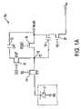
- FIG. 1 ashows an exemplary embodiment of a CMOS imager pixel 10 a of the invention. Similar to most 4T pixels, the pixel 10 a includes a photosensor 12 , floating diffusion node 22 (FD), transfer transistor 14 or transfer gate (TGT), reset transistor 16 , source follower transistor 18 and row select transistor 20 . In the illustrated embodiment, however, the pixel 10 a also includes a dual conversion gain element configured as a transistor 30 (DCGT) and an in-pixel capacitor 32 (CAP). Thus, the pixel 10 a is configured as a novel 5T pixel, the operation of which is described below in more detail. As will become apparent, the dual conversion gain transistor 30 and capacitor 32 form a conversion gain altering circuit for the floating diffusion node 22 .
- DCGTtransistor 30
- CAPin-pixel capacitor 32
- the photosensor 12is a high charge capacity photosensor.
- the high charge capacity photosensor 12may be a photodiode with a high pinning voltage Vpin, a photodiode connected to a capacitor, a photogate, or any similar photosensitive device with a high charge capacity.
- the high charge capacity photosensor 12is a photodiode (PD) with a high Vpin (e.g., 2.3 volts). It should be appreciated, however, that any of the aforementioned photosensors could be used to practice the invention.
- the photosensor 12is coupled to the floating diffusion node 22 via the transfer transistor 14 . It is desirable for the floating diffusion node 22 to have a low capacitance such that it has a high conversion gain of 20 ⁇ V/e to 150 ⁇ V/e or preferably 30 ⁇ V/e to 70 ⁇ V/e.
- the combination of the high charge capacity photosensor 12 and low capacitance floating diffusion node 22is a novel approach and provides a high dynamic range to the pixel 10 a as will become apparent below. In the past, this combination is avoided because the low capacitance floating diffusion node 22 does not have enough charge handling capacity to receive all the collected electrons from the high charge capacity photosensor 12 . In the past, this combination also creates charge sharing and lag issues if exposed to bright light, which are typically to be avoided when designing a pixel due to the image degradation caused by the charge sharing and lag issues. However, as will be discussed below, the use of the high charge capacity photosensor 12 and low capacitance floating diffusion node 22 provides necessary benefits when used in conjunction with the dual conversion gain transistor 30 and capacitor 32 .
- the dual conversion gain transistor 30has its source terminal connected to the floating diffusion node 22 and its drain connected to a first side of the in-pixel capacitor 32 .
- the gate of the dual conversion gain transistor 30is connected to a dual conversion gain control signal DCG.
- the second side of the capacitoris connected to the array pixel supply voltage Vaa-pix.
- the capacitance of the capacitor 32is set such that Q PD ⁇ Q CAP +Q FD , where Q PD is the charge handling capacitance of the photosensor 12 , Q CAP is the charge handling capacitance of the capacitor 32 and Q FD is the charge handling capacitance of the floating diffusion node 22 .
- the dual conversion gain signal (DCG)is generated by the image processor or other control circuit that is controlling the operation of the pixel. This processor or control circuit may utilize additional photosensors or non-imaging pixels to determine the amount of light being processed and to generate the signal accordingly (as discussed below).
- the capacitance of the capacitor 32is switched into the pixel 10 a and coupled to the floating diffusion node 22 when the image processor (or other control circuitry) applies the dual conversion gain control signal DCG to turn on the dual conversion gain transistor 30 .
- the DCG signalmay be generated at different times depending upon the application and/or user preferences.
- FIGS. 1 b – 1 dillustrate other exemplary embodiments of the invention.
- FIG. 1 billustrates a pixel 10 b in which the capacitor 32 is coupled between the dual conversion gain transistor 30 and ground (rather than the array pixel supply voltage Vaa-pix).
- FIG. 1 cillustrates a pixel 10 c in which the positioning of the capacitor 32 and the dual conversion gain transistor 30 are switched (relative to their positions in the FIGS. 1 a and 1 b pixels 10 a , 10 b ).
- FIG. 1 dillustrates another exemplary pixel 10 d in which the positioning of the capacitor 32 and the dual conversion gain transistor 30 are switched (relative to their positions in the FIGS. 1 a and 1 b pixels 10 a , 10 b ) with the modification that the dual conversion gain transistor 30 is coupled to ground (instead of the array pixel supply voltage Vaa-pix).
- the remaining circuitry of the pixels 10 a , 10 b , 10 c , 10 dis connected as follows.
- the reset transistor 16is connected between the floating diffusion node 22 and the array pixel supply voltage Vaa-pix (e.g., 3.3 volts).
- a reset control signal RESETis used to activate the reset transistor 16 , which resets the photosensor 12 and floating diffusion node 22 as is known in the art.
- Vt-resetis the transistor threshold voltage of the reset transistor 16 , typically 0.7 volts. This “overdriving” of the reset transistor 16 allows the floating diffusion node 22 to be reset to the array pixel supply voltage Vaa-pix.
- the source follower transistor 18has its gate connected to the floating diffusion node 22 and is connected between the array pixel supply voltage Vaa-pix and the row select transistor 20 .
- the source follower transistor 18converts the stored charge at the floating diffusion node 22 into an electrical output voltage signal Vout.
- the row select transistor 20is controllable by a row select signal RS for selectively collecting the source follower transistor 18 and the output voltage signal Vout to a column line of a pixel array.
- FIGS. 2 a – 2 dare potential diagrams representing the transfer of charge during an operation of the pixel 10 a under a first light condition.
- FIG. 3is a timing diagram of the operation of the pixel 10 a.
- the row in which the pixel 10 a residesis selected upon the activation of the appropriate row select signal RS.
- the floating diffusion node 22 (FD) and capacitor 32 (CAP) of the activated roware reset by the pulsing on both the reset and dual conversion gain transistors 16 , 30 .
- the reset and dual conversion gain transistors 16 , 30are then turned on to establish the potential diagram shown in FIG. 2 a .
- the illustrated floating diffusion node (FD)is reset to a voltage of Vaa-pix.
- a first sample and hold signal SHRis generated such that sample and hold circuitry connected to a column line of the imager would input, sample and hold any signal at the output of the source follower transistor 18 associated with the reset pixel 10 a.
- FIG. 2 billustrates stored charge in the PD region caused by low light exposure.
- the photodiode charge capacity wellis only slightly filled with the light-generated electrons.
- a transfer gate control signal TGturns on the transfer transistor 14 (TGT), which causes the charge stored in the PD to transfer into the FD node as shown in FIG. 2 c .
- TGTtransfer gate control signal
- the floating diffusion node 22 (FD)has a low capacitance and a high conversion gain because the dual conversion gain transistor 30 remains off. All the electrical charge is transferred from the PD to the FD and there is no charge sharing because the light exposure is low and because Vaa-pix>Vpin.
- Another sample and hold signal SHS 1is generated such that sample and hold circuitry to a column line of the imager would input, sample, and hold the signal associated with the transferred charge (via transistor 18 ). Correlated double sampling may then be used to subtract the sampled exposure signal (SHS 1 ) from the sampled reset signal (SHR) to determine the pixel signal output value change as a result of light exposure to the pixel 10 a.
- the dual conversion gain signal DCGis generated, which activates the dual conversion gain transistor 30 (DCGT) and switches in the capacitance of the capacitor 32 (CAP) as shown by the potential diagram of FIG. 2 d .
- An extremely low signal on the floating diffusion node 22 (FD)results from the added capacitance of the capacitor 32 (CAP).
- Another sample and hold signal SHS 2is generated such that sample and hold circuitry to a column line of the imager would input, sample, and hold the signal associated with this low light charge (via transistor 18 ) with the dual conversion gain transistor 30 now turned “on.” Correlated double sampling may then be used to subtract the sampled exposure signal (SHS 2 ) from the sampled reset signal (SHR) determine the pixel signal output value change as a result of light exposure to the pixel 10 a .
- the image processormay use this pixel output signal change, the previously computed output signal change, or a combination of the two signals depending upon the application. In this manner, a dual conversion gain image sensor is achieved.
- the light signalis first sensed as SHS 1 -SHR with a high conversion gain floating diffusion node (FD) and then sampled again as SHS 2 -SHR with a low conversion gain floating diffusion node (FD).
- FIGS. 1 a , 3 and 4 a – 4 cAn example of the operation of the pixel 10 a under bright or intense light exposure is now described with reference to FIGS. 1 a , 3 and 4 a – 4 c .
- pixel 10 ais reset and the signal associated with the reset condition are obtained as described above with reference to FIG. 2 a .
- the pixel 10 ais exposed to light coming from the image being processed.
- the potential diagram of FIG. 4 aillustrates a charge saturated PD caused by the bright light exposure.
- the PD charge capacity wellis completely filled by electrons generated by the light exposure.
- a transfer gate control signal TGturns on the transfer transistor 14 (TGT), which causes charge sharing between the PD and the floating diffusion node (FD) as shown in FIG. 4 b .
- TGTtransfer transistor 14
- a sample and hold signal SHS 1is generated such that sample and hold circuitry connected to a column line of the imager would input, sample, and hold the signal associated with the saturated shared charge (via transistor 18 ). Correlated double sampling may then be used to subtract the sampled exposure signal (SHS 1 ) from the sampled reset signal (SHR) to determine the pixel signal output value change as a result of the light exposure to the pixel 10 a.
- the dual conversion gain signal DCGis generated, which activates the dual conversion gain transistor 30 (DCGT) and switches in the charge handling capacitance of the capacitor 32 (CAP).
- the charge handling capacitance of the PDis less than the combined charge handling capacitance of the floating diffusion node 22 (FD) and capacitor 32 . This means that there can now be a fill charge transfer to the floating diffusion node 22 , which is now a low conversion gain node due to the additional capacitance as shown in FIG. 4 c . This allows the sampling of a high full well signal when the sample and hold signal SHS 2 is generated. Correlated double sampling may then be used to determine the pixel signal output value change.
- the capacitor 32(CAP) must be carefully chosen.
- the charge handling capacitance of the pinned photodiodeto be:
- the charge handling capacity of the floating diffusion node 22 (FD)is:
- Q FD⁇ Vpin Vaa - pix ⁇ C FD ⁇ d V .
- the capacitance C CAP of the capacitor 32is chosen such that Q PD ⁇ Q FD +Q CAP there will be no charge sharing under bright light exposures when SHS 2 is measured and no resulting image lag issues. While under certain timing applications it is advantageous to appropriately set the capacitance C CAP of the in-pixel capacitor 32 (CAP), this is not a requirement to practice the invention.
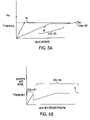
- FIG. 5 ais a graph illustrating pixel signals v. light exposure during the operation of the pixel 10 a illustrated in FIG. 1 a .
- the signal to noise ratio(S/N) is approximately 140 db, which is an acceptable ratio.
- Line 60shows the signal associated with the charge stored in the floating diffusion node 22 when the dual conversion gain transistor 30 is on. That is, when the floating diffusion node 22 has a high capacitance and low conversion gain, line 60 reflects that the output signal Vout does not become saturated at the 20 Ke threshold. If the low conversion gain is set to 5 ⁇ V/e then the output (SHS 2 -SHR) does not become saturated until 200 Ke are collected. At this point, the S/N will have increased to 447 . If the readout noise is e.g., 5 e , then the dynamic range achieved is 100 db.
- 5 bis graph illustrating an adjusted pixel signal 70 that results when the floating diffusion node 22 initially has a high conversion gain that is subsequently switched to a low conversion gain (as discussed above with reference to FIGS. 1–4 ).
- the light dynamic rangehas been improved by ten times. It now takes 10 times more light photons to achieve a saturated SHS 2 -SHR output signal. While FIG. 5 b shows a drop in output signal when the dual conversion gain transistor is turned on, the performance measured by the signal to noise ratio (S/N) is not degraded.
- S/Nsignal to noise ratio
- three sample and hold capacitorsare required to store the three signals SHR, SHS 1 and SHS 2 .
- FIG. 6illustrates a top view of an exemplary layout of the five transistor (5T) pixel 10 a illustrated in FIG. 1 a .
- the capacitor 32is preferably an in-pixel capacitor which may be constructed in accordance with U.S. Pat. No. 6,429,470. It should be appreciated that the pixel 10 a of the present invention does not require the transfer transistor 14 . That is, in another embodiment of the invention the photosensor 12 and the floating diffusion node 22 could be connected without an intervening transistor.
- the dual conversion gain transistor 30 and in-pixel capacitor 32would be controlled in the same manner, would perform the same functions and would change the conversion gain of the floating diffusion node 22 in the same manner as described above with respect to FIGS. 1–5 .
- the inventionis not limited to a pixel containing a transfer gate or transfer transistor.
- Another operating mode for the various embodiments of the inventionis to set a user adjustable gain at the pixel level. That is, the dual conversion gain transistor 30 could be turned on or off for picture taking (as warranted by the light conditions). If the dual conversion gain transistor 30 is off, the conversion gain of the FD node is approximately 50 ⁇ V/e. If the dual conversion gain transistor 30 is on, the conversion gain of the FD is approximately 5 ⁇ V/e. In this operating mode, only two voltage levels are stored in the sample and hold circuitry: (1) a voltage level associated with the reset operation; and (2) the voltage level associated with the charge sent from the photosensor to the floating diffusion node 22 .
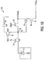
- FIGS. 7–8illustrate a CMOS imager pixel 110 constructed in accordance with another exemplary embodiment of the invention.
- the pixel 110is essentially the same as the pixel 10 a illustrated in FIG. 1 a .
- the pixel 110 of the illustrated embodimentuses a conventional polysilicon in-pixel capacitor 132 and any conventional photosensor 112 .
- FIGS. 7–8illustrate a five transistor (5T) pixel configuration, it should be appreciated that the transfer transistor 14 is not required to practice the invention.
- FIGS. 9 a and 9 bare potential diagrams representing the transfer of charge during an operation of the pixel 110 illustrated in FIG. 7 under a low light condition.
- the pixel 110has been previously reset and is receiving an image signal. Once the photosensor is exposed to the low light, charge accumulates in the PD as shown in FIG. 9 a .
- a transfer gate control signal TGturns on the transfer transistor 14 (TGT), which causes the charge stored in the PD to transfer into the floating diffusion node 22 (FD) as shown in FIG. 9 b .
- TGTtransfer transistor 14
- the floating diffusion node 22 (FD)has a low capacitance and a high conversion gain. There is no charge sharing because the light exposure is low.
- Sample and hold circuitry connected to a column line of the imagerwould input, sample and hold the signal (via transistor 18 ) associated with the charge stored in the floating diffusion node 22 . Correlated double sampling may then be used to determine the pixel signal output value.
- a high conversion gainis desirable. This is achieved by using only the low capacitance floating diffusion node 22 (i.e., the dual conversion gain transistor 30 is not turned on).
- FIGS. 10 a and 10 bare potential diagrams representing the transfer of charge during an operation of the pixel 110 illustrated in FIG. 7 under a bright light condition.
- the pixel 110has been previously reset and is receiving an image signal. Once the photosensor is exposed to the bright light, charge accumulates in the PD ( FIG. 10 a ).
- the potential diagram of FIG. 10 aillustrates a large amount of stored in the PD caused by the bright light exposure.
- a transfer gate control signal TGturns on the transfer transistor 14 and the dual conversion gain signal DCG activates the dual conversion gain transistor 30 (DCGT) to switch in the capacitance of the capacitor 132 (CAP).
- the dual conversion gain signal (DCG)is generated by the image processor or other control circuit that is controlling the operation of the pixel.
- the transfer gate control signal TG and the dual conversion gain signal DCGmay be generated simultaneously or substantially simultaneously.
- the charge handling capacitance of the PDis less than the combined charge handling capacitance of the floating diffusion node 22 and capacitor 132 . This means that there can now be a full charge transfer to the floating diffusion node 22 node, which is now a low conversion gain node due to the additional charge handling capacitance. This allows the sampling of the high full well signal.
- FIG. 11is a portion of a CCD imager 200 constructed in accordance with an exemplary embodiment of the invention.
- the CCD imager 200includes a shift register 202 for shifting charges input from a photosensitive device of the imager 200 .
- the register 202is often referred to as the charge coupled device of the CCD imager 200 .
- a final or output stage 204 of the register 202is coupled to the floating diffusion node 22 . Coupled between the floating diffusion node 22 and a supply voltage Vcc is a gate 206 of a reset transistor.
- a source follower transistor 208has its gate connected to the floating diffusion node 22 .
- the source follower transistor 208is coupled between the supply voltage Vcc and a load 214 and outputs a signal Vout corresponding to stored charge on the floating diffusion node 22 . All of the circuitry described so far is conventional and known in the CCD imager art.
- the illustrated imager 200also includes a dual conversion gain transistor 210 (DCGT) and a capacitor 212 (CAP).
- the dual conversion gain transistor 210is coupled between the floating diffusion node 22 and the capacitor 212 and is controlled by a dual conversion gain control signal DCG.
- the capacitor 212is connected between the dual conversion gain transistor 210 and the supply voltage Vcc.
- the dual conversion gain transistor 210 and capacitor 212are used to switch the conversion gain of the floating diffusion node 22 from a first or high conversion gain state (i.e., DCG is generated such that the dual conversion gain transistor 210 is off and capacitor 212 switched out of the imager 200 ) to a second or low conversion gain state (i.e., DCG is generated such that the dual conversion gain transistor 210 is on and capacitor 212 connected to the floating diffusion node 22 ).
- DCGhigh conversion gain state
- DCGlow conversion gain state
- the dual conversion gain transistor 210 and capacitor 212provide dual conversion gain capability to the CCD imager 200 , which yields high dynamic range and excellent low light performance.
- FIG. 12illustrates a block diagram for a CMOS imager device 308 having a pixel array 225 incorporating pixels 10 , 110 constructed in the manner discussed above in relation to FIGS. 1–10 .
- Pixel array 225comprises a plurality of pixels arranged in a predetermined number of columns and rows. The pixels of each row in array 225 can all be turned on at the same time by a row select line and the pixels of each column are selectively output by a column select line. A plurality of rows and column lines are provided for the entire array 225 .
- the row linesare selectively activated by the row driver 240 in response to row address decoder 230 and the column select lines are selectively activated by the column driver 260 in response to column address decoder 270 .
- a row and column addressis provided for each pixel in the array 225 .
- the CMOS imager device 308is operated by the control circuit 250 , which controls address decoders 230 , 270 for selecting the appropriate row and column lines for pixel readout, and row and column driver circuitry 240 , 260 , which apply driving voltages to the drive transistors of the selected row and column lines.
- the signal flow in the imager device 308would begin at the array 225 upon its receiving photo-input and generating a charge.
- the signalis output to a read-out circuit and then to an analog-to-digital conversion device. Then the signal is transferred to an image processor, a serializer and then the is output from the imager device.
- FIG. 13shows system 300 , a typical processor based system modified to include an imager device 308 as in FIG. 12 and an input device to the system 300 .
- the imager device 308may also receive control or other data from system 300 as well.
- Examples of processor based systems, which may employ the imager device 308include, without limitation, computer systems, camera systems, scanners, machine vision systems, vehicle navigation systems, video telephones, surveillance systems, auto focus systems, star tracker systems, motion detection systems, image stabilization systems, and others.
- System 300includes a central processing unit (CPU) 302 that communicates with various devices over a bus 304 .
- Some of the devices connected to the bus 304provide communication into and out of the system 300 , illustratively including an input/output (I/O) device 306 and imager device 308 .
- Other devices connected to the bus 304provide memory, illustratively including a random access memory (RAM) 310 , hard drive 312 , and one or more peripheral memory devices such as a floppy disk drive 314 and compact disk (CD) drive 316 .
- the imager device 308may be combined with a processor, such as a CPU, digital signal processor, or microprocessor, in a single integrated circuit.
- the imager device 308may be a CCD imager or CMOS imager constructed in accordance with any of the illustrated embodiments.
- the present inventionprovides imagers with (1) high conversion gain and sensitivity to achieve excellent low light performance and (2) high full well capacity and conversion gain to achieve high dynamic range—something that is not achievable with current image technology.
- the dual conversion gain principles of the inventioncould be incorporated into many different imager devices (CCD or CMOS) and imager configurations (e.g., two transistor (2T), 3T, 4T, etc.).
- the principles of the inventionmay be utilized with any capacitor-transistor series structure.
- the inventionis not limited solely to dual conversion gain principles. That is, a floating diffusion node could be connected to multiple dual conversion gain transistors and associated capacitors to provide the floating diffusion node with more than two conversion gains if desired.
- FIG. 3it is possible to use other timings. For example, there can be applications where one allows the capacitor 32 to be chosen so that there is charge sharing during SHS 2 sampling.
Landscapes
- Engineering & Computer Science (AREA)
- Multimedia (AREA)
- Signal Processing (AREA)
- Solid State Image Pick-Up Elements (AREA)
- Transforming Light Signals Into Electric Signals (AREA)
Abstract
Description
The charge handling capacity of the capacitor32 (CAP) is: QCAP=CCAP[Vaa-pix−Vpin]. As long as the capacitance CCAPof the
Claims (121)
Priority Applications (8)
| Application Number | Priority Date | Filing Date | Title |
|---|---|---|---|
| US10/458,262US7075049B2 (en) | 2003-06-11 | 2003-06-11 | Dual conversion gain imagers |
| JP2006533670AJP4372789B2 (en) | 2003-06-11 | 2004-06-10 | Two-stage conversion gain imager |
| EP04754892AEP1636983A1 (en) | 2003-06-11 | 2004-06-10 | Dual conversion gain imagers |
| PCT/US2004/018425WO2004112376A1 (en) | 2003-06-11 | 2004-06-10 | Dual conversion gain imagers |
| CN2004800225832ACN1833429B (en) | 2003-06-11 | 2004-06-10 | Dual conversion gain imagers |
| KR1020077008646AKR100871056B1 (en) | 2003-06-11 | 2004-06-10 | Dual conversion gain imagers |
| KR1020057023887AKR100763442B1 (en) | 2003-06-11 | 2004-06-10 | Dual conversion gain imagers |
| TW093116992ATWI259577B (en) | 2003-06-11 | 2004-06-11 | Dual conversion gain imagers |
Applications Claiming Priority (1)
| Application Number | Priority Date | Filing Date | Title |
|---|---|---|---|
| US10/458,262US7075049B2 (en) | 2003-06-11 | 2003-06-11 | Dual conversion gain imagers |
Publications (2)
| Publication Number | Publication Date |
|---|---|
| US20040251394A1 US20040251394A1 (en) | 2004-12-16 |
| US7075049B2true US7075049B2 (en) | 2006-07-11 |
Family
ID=33510548
Family Applications (1)
| Application Number | Title | Priority Date | Filing Date |
|---|---|---|---|
| US10/458,262Expired - LifetimeUS7075049B2 (en) | 2003-06-11 | 2003-06-11 | Dual conversion gain imagers |
Country Status (7)
| Country | Link |
|---|---|
| US (1) | US7075049B2 (en) |
| EP (1) | EP1636983A1 (en) |
| JP (1) | JP4372789B2 (en) |
| KR (2) | KR100763442B1 (en) |
| CN (1) | CN1833429B (en) |
| TW (1) | TWI259577B (en) |
| WO (1) | WO2004112376A1 (en) |
Cited By (71)
| Publication number | Priority date | Publication date | Assignee | Title |
|---|---|---|---|---|
| US20060181622A1 (en)* | 2003-07-15 | 2006-08-17 | Micron Technology, Inc. | 4T CMOS image sensor with floating diffusion gate capacitor |
| US20060243887A1 (en)* | 2004-04-07 | 2006-11-02 | Christian Boemler | High dynamic range pixel amplifier |
| US20070164332A1 (en)* | 2006-01-13 | 2007-07-19 | Kee-Hyun Paik | Shared-pixel-type image sensors for controlling capacitance of floating diffusion region |
| US20070285547A1 (en)* | 2006-05-30 | 2007-12-13 | Milligan Edward S | CMOS image sensor array optimization for both bright and low light conditions |
| US20080173909A1 (en)* | 2007-01-19 | 2008-07-24 | Christopher Parks | Image sensor with gain control |
| US20080273104A1 (en)* | 2007-05-01 | 2008-11-06 | Christopher Parks | Image sensor pixel with gain control |
| US20080303905A1 (en)* | 2007-06-08 | 2008-12-11 | Micron Technology, Inc. | Methods and apparatuses for non-optical pixel self test |
| US20090066782A1 (en)* | 2007-09-07 | 2009-03-12 | Regents Of The University Of Minnesota | Spatial-temporal multi-resolution image sensor with adaptive frame rates for tracking movement in a region of interest |
| US20090194672A1 (en)* | 2008-02-04 | 2009-08-06 | Tredwell Timothy J | Digital radiographic imaging apparatus |
| US20090272879A1 (en)* | 2008-04-30 | 2009-11-05 | Omnivision Technologies, Inc. | High conversion gain image sensor |
| US20090294632A1 (en)* | 2008-05-30 | 2009-12-03 | Omnivision Technologies, Inc. | Globally reset image sensor pixels |
| US20100277607A1 (en)* | 2007-09-28 | 2010-11-04 | Regents Of The University Of Minnesota | Image sensor with high dynamic range imaging and integrated motion detection |
| US20100276574A1 (en)* | 2009-04-30 | 2010-11-04 | Omnivision Technologies, Inc. | Image sensor with global shutter |
| US20110187906A1 (en)* | 2008-04-10 | 2011-08-04 | Chaji G Reza | Gain adjustable sensor pixels, arrays and array systems and methods therefor |
| WO2011091785A1 (en) | 2010-01-28 | 2011-08-04 | Conti Temic Microelectronic Gmbh | Highly dynamic image sensor for detecting modulated light |
| US8077237B2 (en) | 2007-10-16 | 2011-12-13 | Aptina Imaging Corporation | Method and apparatus for controlling dual conversion gain signal in imaging devices |
| US20120261549A1 (en)* | 2011-04-13 | 2012-10-18 | Lg Innotek Co., Ltd. | Pixel, pixel array, and image sensor including pixel array |
| US8294077B2 (en) | 2010-12-17 | 2012-10-23 | Omnivision Technologies, Inc. | Image sensor having supplemental capacitive coupling node |
| RU2467432C1 (en)* | 2010-06-24 | 2012-11-20 | Кэнон Кабусики Кайся | Solid-state imaging device and method for driving solid-state imaging device |
| US8575533B2 (en) | 2011-04-08 | 2013-11-05 | PixArt Imaging Incorporation, R.O.C. | High dynamic range imager circuit and method for reading high dynamic range image |
| US8729451B2 (en) | 2011-08-30 | 2014-05-20 | Omnivision Technologies, Inc. | Multilevel reset voltage for multi-conversion gain image sensor |
| US9106851B2 (en) | 2013-03-12 | 2015-08-11 | Tower Semiconductor Ltd. | Single-exposure high dynamic range CMOS image sensor pixel with internal charge amplifier |
| US20150319384A1 (en)* | 2014-05-01 | 2015-11-05 | Canon Kabushiki Kaisha | Solid-state imaging device and method of driving the same |
| US9287009B2 (en) | 2014-05-12 | 2016-03-15 | Samsung Electronics Co., Ltd. | Repair circuit and fuse circuit |
| US9337223B2 (en) | 2013-11-25 | 2016-05-10 | Semiconductor Components Industriess, Llc | Imaging systems with image pixels having adjustable responsivity |
| US9729808B2 (en) | 2013-03-12 | 2017-08-08 | Tower Semiconductor Ltd. | Single-exposure high dynamic range CMOS image sensor pixel with internal charge amplifier |
| US9741754B2 (en) | 2013-03-06 | 2017-08-22 | Apple Inc. | Charge transfer circuit with storage nodes in image sensors |
| US9743027B2 (en) | 2015-06-24 | 2017-08-22 | Semiconductor Components Industries, Llc | Image sensor with high dynamic range and method |
| US9843738B2 (en) | 2015-10-01 | 2017-12-12 | Semiconductor Components Industries, Llc | High dynamic range imaging pixels with improved readout |
| US20170359521A1 (en)* | 2016-06-09 | 2017-12-14 | SK Hynix Inc. | Pixel signal transfer device and method thereof and cmos image sensor including the same |
| US20170373107A1 (en)* | 2015-01-29 | 2017-12-28 | Sony Semiconductor Solutions Corporation | Solid-state image sensing device and electronic device |
| US9888191B2 (en) | 2015-04-21 | 2018-02-06 | Semiconductor Components Industries, Llc | Imaging systems and methods for performing unboosted image sensor pixel conversion gain adjustments |
| US9912883B1 (en) | 2016-05-10 | 2018-03-06 | Apple Inc. | Image sensor with calibrated column analog-to-digital converters |
| US9929204B2 (en)* | 2014-03-13 | 2018-03-27 | Samsung Electronics Co., Ltd. | Unit pixel of image sensor, image sensor including the same and method of manufacturing image sensor |
| US9948875B2 (en) | 2015-10-01 | 2018-04-17 | Semiconductor Components Industries, Llc | High dynamic range imaging pixels with improved readout |
| US10110839B2 (en) | 2016-05-03 | 2018-10-23 | Semiconductor Components Industries, Llc | Dual-photodiode image pixel |
| US10170514B2 (en) | 2013-10-17 | 2019-01-01 | Cmosis Bvba | Image sensor |
| US10250826B2 (en) | 2016-01-15 | 2019-04-02 | Invisage Technologies, Inc. | Image sensors having extended dynamic range |
| US10263032B2 (en) | 2013-03-04 | 2019-04-16 | Apple, Inc. | Photodiode with different electric potential regions for image sensors |
| US10285626B1 (en) | 2014-02-14 | 2019-05-14 | Apple Inc. | Activity identification using an optical heart rate monitor |
| US10438987B2 (en) | 2016-09-23 | 2019-10-08 | Apple Inc. | Stacked backside illuminated SPAD array |
| US10440301B2 (en) | 2017-09-08 | 2019-10-08 | Apple Inc. | Image capture device, pixel, and method providing improved phase detection auto-focus performance |
| US10609348B2 (en) | 2014-05-30 | 2020-03-31 | Apple Inc. | Pixel binning in an image sensor |
| US10622538B2 (en) | 2017-07-18 | 2020-04-14 | Apple Inc. | Techniques for providing a haptic output and sensing a haptic input using a piezoelectric body |
| US10656251B1 (en) | 2017-01-25 | 2020-05-19 | Apple Inc. | Signal acquisition in a SPAD detector |
| US10681291B2 (en) | 2015-06-08 | 2020-06-09 | Panasonic Intellectual Property Management Co., Ltd. | Imaging device including photoelectric converter |
| US10741592B2 (en) | 2018-06-07 | 2020-08-11 | Semiconductor Components Industries, Llc | Image sensors with multi-photodiode image pixels and vertical transfer gates |
| US10770491B2 (en) | 2014-12-26 | 2020-09-08 | Panasonic Intellectual Property Management Co., Ltd. | Imaging device including photoelectric converter and capacitor with a capacitor and a switching element connected in series between a first electrode of a photoelectric converter and a voltage source or a ground |
| US10801886B2 (en) | 2017-01-25 | 2020-10-13 | Apple Inc. | SPAD detector having modulated sensitivity |
| US10848693B2 (en) | 2018-07-18 | 2020-11-24 | Apple Inc. | Image flare detection using asymmetric pixels |
| US10962628B1 (en) | 2017-01-26 | 2021-03-30 | Apple Inc. | Spatial temporal weighting in a SPAD detector |
| US11019294B2 (en) | 2018-07-18 | 2021-05-25 | Apple Inc. | Seamless readout mode transitions in image sensors |
| US11114482B2 (en) | 2019-11-20 | 2021-09-07 | Gigajot Technology, Inc. | Scalable-pixel-size image sensor |
| US11233966B1 (en) | 2018-11-29 | 2022-01-25 | Apple Inc. | Breakdown voltage monitoring for avalanche diodes |
| US11336842B2 (en) | 2019-01-08 | 2022-05-17 | Panasonic Intellectual Property Management Co., Ltd. | Imaging device |
| US20220217291A1 (en)* | 2021-01-04 | 2022-07-07 | Samsung Electronics Co., Ltd. | Image sensor, pixel, and method of operating the pixel |
| US11528439B2 (en) | 2020-02-28 | 2022-12-13 | Samsung Electronics Co., Ltd. | Image sensor, image processing system including the same, and operating method of the same |
| US11546532B1 (en) | 2021-03-16 | 2023-01-03 | Apple Inc. | Dynamic correlated double sampling for noise rejection in image sensors |
| US11563910B2 (en) | 2020-08-04 | 2023-01-24 | Apple Inc. | Image capture devices having phase detection auto-focus pixels |
| US11658201B2 (en) | 2021-08-25 | 2023-05-23 | Silead Inc. | Dual conversion gain image sensor pixels |
| US11665451B2 (en) | 2019-11-27 | 2023-05-30 | Samsung Electronics Co., Ltd. | Image sensor, imaging device having the image sensor, and operating method thereof |
| US11722795B2 (en) | 2021-06-25 | 2023-08-08 | Samsung Electronics Co., Ltd. | Image processing device for noise reduction using dual conversion gain and operation method thereof |
| US11743610B2 (en) | 2021-06-21 | 2023-08-29 | Samsung Electronics Co., Ltd. | Pixel and image sensor including the same |
| US11950011B2 (en) | 2021-11-04 | 2024-04-02 | Samsung Electronics Co., Ltd. | Image sensor |
| US11956557B1 (en) | 2022-10-17 | 2024-04-09 | BAE Systems Imaging Solutions Inc. | Pixel architecture with high dynamic range |
| US12069384B2 (en) | 2021-09-23 | 2024-08-20 | Apple Inc. | Image capture devices having phase detection auto-focus pixels |
| US12192644B2 (en) | 2021-07-29 | 2025-01-07 | Apple Inc. | Pulse-width modulation pixel sensor |
| US12267605B2 (en) | 2022-10-17 | 2025-04-01 | Fairchild Imaging, Inc. | Pixel architecture with multiple pixel binning |
| US12294011B2 (en) | 2021-07-28 | 2025-05-06 | Magvision Semiconductor (Beijing) Inc. | Image sensor pixel with deep trench isolation structure |
| US12356740B2 (en) | 2020-09-25 | 2025-07-08 | Apple Inc. | Transistor integration with stacked single-photon avalanche diode (SPAD) pixel arrays |
| US12432473B2 (en) | 2023-02-01 | 2025-09-30 | Samsung Electronics Co., Ltd. | Image sensing device and electric apparatus including the same |
Families Citing this family (99)
| Publication number | Priority date | Publication date | Assignee | Title |
|---|---|---|---|---|
| US6780666B1 (en)* | 2003-08-07 | 2004-08-24 | Micron Technology, Inc. | Imager photo diode capacitor structure with reduced process variation sensitivity |
| US7196304B2 (en)* | 2004-01-29 | 2007-03-27 | Micron Technology, Inc. | Row driver for selectively supplying operating power to imager pixel |
| EP1732134B1 (en)* | 2004-02-27 | 2012-10-24 | National University Corporation Tohoku Unversity | Solid-state imagine device, line sensor, optical sensor, and method for operating solid-state imaging device |
| US20060103749A1 (en)* | 2004-11-12 | 2006-05-18 | Xinping He | Image sensor and pixel that has switchable capacitance at the floating node |
| US7518645B2 (en)* | 2005-01-06 | 2009-04-14 | Goodrich Corp. | CMOS active pixel sensor with improved dynamic range and method of operation |
| US7551059B2 (en)* | 2005-01-06 | 2009-06-23 | Goodrich Corporation | Hybrid infrared detector array and CMOS readout integrated circuit with improved dynamic range |
| US7616231B2 (en)* | 2005-01-06 | 2009-11-10 | Goodrich Corporation | CMOS active pixel sensor with improved dynamic range and method of operation for object motion detection |
| WO2006073875A2 (en)* | 2005-01-06 | 2006-07-13 | Recon/Optical, Inc. | Cmos active pixel sensor with improved dynamic range and method of operation, method for identifying moving objects and hybrid array with ir detector |
| JP4416668B2 (en)* | 2005-01-14 | 2010-02-17 | キヤノン株式会社 | Solid-state imaging device, control method thereof, and camera |
| US7568628B2 (en) | 2005-03-11 | 2009-08-04 | Hand Held Products, Inc. | Bar code reading device with global electronic shutter control |
| EP3300359B1 (en)* | 2005-03-11 | 2021-06-30 | Hand Held Products, Inc. | Bar code reading device with global electronic shutter control |
| US7780089B2 (en) | 2005-06-03 | 2010-08-24 | Hand Held Products, Inc. | Digital picture taking optical reader having hybrid monochrome and color image sensor array |
| US7611060B2 (en) | 2005-03-11 | 2009-11-03 | Hand Held Products, Inc. | System and method to automatically focus an image reader |
| US7718459B2 (en)* | 2005-04-15 | 2010-05-18 | Aptina Imaging Corporation | Dual conversion gain pixel using Schottky and ohmic contacts to the floating diffusion region and methods of fabrication and operation |
| JP4340640B2 (en)* | 2005-04-20 | 2009-10-07 | シャープ株式会社 | Amplification type solid-state imaging device |
| US7830437B2 (en)* | 2005-05-11 | 2010-11-09 | Aptina Imaging Corp. | High fill factor multi-way shared pixel |
| US7479995B2 (en)* | 2005-05-19 | 2009-01-20 | Digital Imaging Systems Gmbh | On chip real time FPN correction without imager size memory |
| US7770799B2 (en) | 2005-06-03 | 2010-08-10 | Hand Held Products, Inc. | Optical reader having reduced specular reflection read failures |
| US7468532B2 (en)* | 2005-07-12 | 2008-12-23 | Aptina Imaging Corporation | Method and apparatus providing capacitor on an electrode of an imager photosensor |
| US7728896B2 (en)* | 2005-07-12 | 2010-06-01 | Micron Technology, Inc. | Dual conversion gain gate and capacitor and HDR combination |
| US7432540B2 (en) | 2005-08-01 | 2008-10-07 | Micron Technology, Inc. | Dual conversion gain gate and capacitor combination |
| US20070035649A1 (en)* | 2005-08-10 | 2007-02-15 | Micron Technology, Inc. | Image pixel reset through dual conversion gain gate |
| JP4861015B2 (en)* | 2006-01-13 | 2012-01-25 | キヤノン株式会社 | Imaging device and imaging apparatus |
| JP3996618B1 (en)* | 2006-05-11 | 2007-10-24 | 総吉 廣津 | Semiconductor image sensor |
| ITMN20060040A1 (en)* | 2006-05-19 | 2007-11-20 | Pe Srl | CUTTING DEVICE FOR A TAPE IN PAPER, PLASTIC OR SIMILAR MATERIAL |
| US7969490B2 (en) | 2006-08-25 | 2011-06-28 | Micron Technology, Inc. | Method, apparatus, and system providing an imager with pixels having extended dynamic range |
| JP2008205638A (en)* | 2007-02-16 | 2008-09-04 | Texas Instr Japan Ltd | Solid-state imaging device and operation method thereof |
| JP2008205639A (en)* | 2007-02-16 | 2008-09-04 | Texas Instr Japan Ltd | Solid-state imaging device and operation method thereof |
| US7674648B2 (en)* | 2007-03-21 | 2010-03-09 | Eastman Kodak Company | Extended dynamic range using variable sensitivity pixels |
| JP4389959B2 (en)* | 2007-04-23 | 2009-12-24 | ソニー株式会社 | Solid-state imaging device, signal processing method for solid-state imaging device, and imaging device |
| JP4935486B2 (en)* | 2007-04-23 | 2012-05-23 | ソニー株式会社 | Solid-state imaging device, driving method for solid-state imaging device, signal processing method for solid-state imaging device, and imaging device |
| KR100847742B1 (en)* | 2007-08-20 | 2008-07-22 | 배정훈 | Common Column Active CMOS Image Sensor with Adjustable Conversion Gain |
| KR101437689B1 (en)* | 2007-12-28 | 2014-09-05 | 엘지디스플레이 주식회사 | Photoelectric sensor and its driving method |
| US20090237540A1 (en)* | 2008-03-20 | 2009-09-24 | Micron Technology, Inc. | Imager method and apparatus having combined gate signals |
| KR101465667B1 (en)* | 2008-03-25 | 2014-11-26 | 삼성전자주식회사 | CMOS image sensor and driving method therof |
| US8232771B2 (en) | 2008-12-08 | 2012-07-31 | Apple Inc. | Battery gas gauge reset mechanism |
| US8174602B2 (en)* | 2009-01-15 | 2012-05-08 | Raytheon Company | Image sensing system and method utilizing a MOSFET |
| US8233070B2 (en)* | 2009-03-27 | 2012-07-31 | International Business Machines Corporation | Variable dynamic range pixel sensor cell, design structure and method |
| US9131142B2 (en) | 2009-07-17 | 2015-09-08 | Nikon Corporation | Focusing device and camera |
| US20110074996A1 (en)* | 2009-09-29 | 2011-03-31 | Shen Wang | Ccd image sensors with variable output gains in an output circuit |
| JP5511541B2 (en) | 2010-06-24 | 2014-06-04 | キヤノン株式会社 | Solid-state imaging device and driving method of solid-state imaging device |
| KR101476610B1 (en)* | 2010-09-05 | 2014-12-24 | 뉴포트 코포레이션 | Multi-junction detector system |
| US8847136B2 (en) | 2011-01-02 | 2014-09-30 | Pixim, Inc. | Conversion gain modulation using charge sharing pixel |
| US8896733B2 (en) | 2011-01-21 | 2014-11-25 | Aptina Imaging Corporation | Imaging system with automatic conversion gain selection |
| CN102104744B (en)* | 2011-03-04 | 2013-01-16 | 北京思比科微电子技术股份有限公司 | CMOS image sensor pixel reading circuit structure and pixel structure |
| US8643132B2 (en)* | 2011-06-08 | 2014-02-04 | Omnivision Technologies, Inc. | In-pixel high dynamic range imaging |
| KR101838894B1 (en) | 2011-07-08 | 2018-03-16 | 삼성전자주식회사 | Image sensor, and image processing device including the same |
| JP2013034045A (en)* | 2011-08-01 | 2013-02-14 | Sony Corp | Solid-state imaging device and imaging device |
| JP5915031B2 (en)* | 2011-08-31 | 2016-05-11 | ソニー株式会社 | IMAGING DEVICE, IMAGING METHOD, AND ELECTRONIC DEVICE |
| CN102544050A (en)* | 2011-12-28 | 2012-07-04 | 上海中科高等研究院 | Charge storage unit and image sensor pixel circuit |
| KR20130085124A (en)* | 2012-01-19 | 2013-07-29 | 삼성전자주식회사 | Image sensor and portable device having the same |
| TWI533699B (en)* | 2012-01-27 | 2016-05-11 | Sony Corp | A solid-state imaging element and a driving method, and an electronic device |
| CN103297720A (en)* | 2012-02-23 | 2013-09-11 | 联咏科技股份有限公司 | Light sensing pixel circuit and image sensor |
| CN102593139A (en)* | 2012-02-28 | 2012-07-18 | 上海宏力半导体制造有限公司 | CMOS (Complementary Metal-Oxide-Semiconductor Transistor) image sensor |
| US9093351B2 (en)* | 2012-03-21 | 2015-07-28 | Canon Kabushiki Kaisha | Solid-state imaging apparatus |
| JP2014112580A (en) | 2012-12-05 | 2014-06-19 | Sony Corp | Solid-state image sensor and driving method |
| CN104144305B (en)* | 2013-05-10 | 2017-08-11 | 江苏思特威电子科技有限公司 | Dual conversion gain imaging device and its imaging method |
| FR3008826A1 (en)* | 2013-07-18 | 2015-01-23 | St Microelectronics Crolles 2 | IMAGE SENSOR CELL WITH DUAL CONVERSION GAIN |
| US9277147B2 (en) | 2013-08-23 | 2016-03-01 | Semiconductor Components Industries, Llc | Multimode pixel readout for enhanced dynamic range |
| US9363450B2 (en)* | 2013-08-27 | 2016-06-07 | Semiconductor Components Industries, Llc | Imaging systems and methods for image signal gain adjustment |
| FR3010229B1 (en)* | 2013-08-30 | 2016-12-23 | Pyxalis | IMAGE SENSOR WITH REDUCED KTC NOISE |
| US9147704B2 (en)* | 2013-11-11 | 2015-09-29 | Omnivision Technologies, Inc. | Dual pixel-sized color image sensors and methods for manufacturing the same |
| US9473706B2 (en)* | 2013-12-09 | 2016-10-18 | Apple Inc. | Image sensor flicker detection |
| US9402039B2 (en)* | 2014-01-10 | 2016-07-26 | Omnivision Technologies, Inc. | Dual conversion gain high dynamic range sensor |
| CN110233978B (en)* | 2014-02-07 | 2022-03-11 | 拉姆伯斯公司 | Feedthrough compensated image sensor |
| GB2525625B (en) | 2014-04-29 | 2017-05-31 | Isdi Ltd | Device and method |
| FR3022397B1 (en) | 2014-06-13 | 2018-03-23 | New Imaging Technologies | C-MOS PHOTOELECTRIC CELL WITH CHARGE TRANSFER, AND MATRIX SENSOR COMPRISING AN ENSEMBLE OF SUCH CELLS |
| JP6700656B2 (en)* | 2014-10-31 | 2020-05-27 | キヤノン株式会社 | Imaging device |
| JP6650668B2 (en)* | 2014-12-16 | 2020-02-19 | キヤノン株式会社 | Solid-state imaging device |
| JP2018513570A (en)* | 2015-03-31 | 2018-05-24 | ダートマス カレッジ | Image sensor having JFET source follower and image sensor pixel |
| TWI572023B (en) | 2015-04-15 | 2017-02-21 | 力晶科技股份有限公司 | CMOS image sensing unit and manufacturing method thereof |
| TWI701819B (en)* | 2015-06-09 | 2020-08-11 | 日商索尼半導體解決方案公司 | Imaging element, driving method and electronic equipment |
| US20240006430A1 (en)* | 2015-08-18 | 2024-01-04 | Sri International | Multiresolution imager for night vision |
| CN105163044B (en)* | 2015-09-09 | 2018-02-09 | 长春长光辰芯光电技术有限公司 | High dynamic range image sensor data output method and device |
| JP2017055248A (en) | 2015-09-09 | 2017-03-16 | ルネサスエレクトロニクス株式会社 | Imaging device |
| CN105208301B (en)* | 2015-09-16 | 2018-06-22 | 上海集成电路研发中心有限公司 | The pixel cell structure and its signal acquisition method of dual conversion gain |
| CN105208302B (en)* | 2015-09-16 | 2018-06-22 | 上海集成电路研发中心有限公司 | Pixel cell structure and its signal acquisition method |
| JP6663209B2 (en)* | 2015-11-30 | 2020-03-11 | キヤノン株式会社 | Imaging device, imaging system, and driving method of imaging device |
| DE112017001031T5 (en) | 2016-02-29 | 2019-01-03 | Sony Corporation | Solid-state imaging device |
| CN109155322B (en)* | 2016-06-08 | 2023-02-21 | 因维萨热技术公司 | Image sensor with electronic shutter |
| DE102016212784A1 (en) | 2016-07-13 | 2018-01-18 | Robert Bosch Gmbh | CMOS pixel, image sensor and camera and method for reading out a CMOS pixel |
| CN106162003B (en)* | 2016-08-24 | 2023-06-27 | 京东方科技集团股份有限公司 | A reading circuit and its driving method, X-ray pixel circuit |
| KR102678455B1 (en)* | 2016-12-30 | 2024-06-27 | 삼성전자주식회사 | Image sensor |
| US10582138B2 (en)* | 2017-09-22 | 2020-03-03 | Semiconductor Components Industries, Llc | Image sensors with dual conversion gain pixels and anti-eclipse circuitry |
| US10455162B2 (en)* | 2018-01-23 | 2019-10-22 | Semiconductor Components Industries, Llc | Imaging pixels with storage capacitors |
| US10560649B2 (en)* | 2018-02-20 | 2020-02-11 | Semiconductor Components Industries, Llc | Imaging systems having dual storage gate overflow capabilities |
| CN108470742B (en)* | 2018-03-22 | 2020-10-02 | 思特威(上海)电子科技有限公司 | HDR image sensor pixel structure and imaging system |
| US10923523B2 (en)* | 2018-04-16 | 2021-02-16 | Facebook Technologies, Llc | Multi-photodiode pixel cell |
| CN108495064B (en)* | 2018-06-20 | 2023-12-15 | 思特威(上海)电子科技股份有限公司 | Pixel circuit and image sensor device |
| JP7245016B2 (en) | 2018-09-21 | 2023-03-23 | キヤノン株式会社 | Photoelectric conversion device and imaging system |
| US11405568B2 (en) | 2018-11-07 | 2022-08-02 | Sony Semiconductor Solutions Corporation | Imaging apparatus and electronic device |
| US20220038648A1 (en)* | 2018-12-11 | 2022-02-03 | Sony Semiconductor Solutions Corporation | Solid-state imaging device and electronic device |
| JP7341659B2 (en)* | 2018-12-25 | 2023-09-11 | ブリルニクス シンガポール プライベート リミテッド | Solid-state imaging device, driving method for solid-state imaging device, and electronic equipment |
| CN114785964B (en)* | 2019-08-14 | 2024-03-01 | 原相科技股份有限公司 | Image pickup system having two exposure modes |
| KR102721299B1 (en) | 2019-11-12 | 2024-10-25 | 삼성전자주식회사 | Image senosor, image device having the same, and operating method therof |
| KR20210156458A (en) | 2020-06-18 | 2021-12-27 | 삼성전자주식회사 | Image sensing device and electronic device comprising the same |
| CN114765670B (en)* | 2021-01-13 | 2024-11-12 | 格科微电子(上海)有限公司 | Implementation method of multi-conversion gain image sensor and electronic information device |
| CN116055890B (en)* | 2022-08-29 | 2024-08-02 | 荣耀终端有限公司 | Method and electronic device for generating high dynamic range video |
| CN115988348B (en)* | 2023-03-22 | 2023-06-09 | 深圳锐视智芯科技有限公司 | Image sensor, image output method thereof and photoelectric equipment |
Citations (18)
| Publication number | Priority date | Publication date | Assignee | Title |
|---|---|---|---|---|
| US4734776A (en) | 1986-08-15 | 1988-03-29 | General Electric Company | Readout circuit for an optical sensing charge injection device facilitating an extended dynamic range |
| US5049752A (en) | 1990-10-31 | 1991-09-17 | Grumman Aerospace Corporation | Scanning circuit |
| EP0498664A1 (en) | 1991-02-08 | 1992-08-12 | Sharp Kabushiki Kaisha | Solid-state imaging device |
| US5355165A (en) | 1992-08-06 | 1994-10-11 | Princeton Scientific Instruments, Inc. | Very high frame rate CCD imager |
| US5396288A (en) | 1992-08-21 | 1995-03-07 | Fuji Photo Film Co., Ltd. | Image processing apparatus and method, and video camera |
| US5422669A (en) | 1991-12-13 | 1995-06-06 | Sony Corporation | Solid state imaging apparatus |
| US5841126A (en) | 1994-01-28 | 1998-11-24 | California Institute Of Technology | CMOS active pixel sensor type imaging system on a chip |
| US6069376A (en) | 1998-03-26 | 2000-05-30 | Foveonics, Inc. | Intra-pixel frame storage element, array, and electronic shutter method including speed switch suitable for electronic still camera applications |
| US6140630A (en) | 1998-10-14 | 2000-10-31 | Micron Technology, Inc. | Vcc pump for CMOS imagers |
| US6204524B1 (en) | 1999-07-14 | 2001-03-20 | Micron Technology, Inc. | CMOS imager with storage capacitor |
| US6246436B1 (en) | 1997-11-03 | 2001-06-12 | Agilent Technologies, Inc | Adjustable gain active pixel sensor |
| US6310366B1 (en) | 1999-06-16 | 2001-10-30 | Micron Technology, Inc. | Retrograde well structure for a CMOS imager |
| US6326652B1 (en) | 1999-06-18 | 2001-12-04 | Micron Technology, Inc., | CMOS imager with a self-aligned buried contact |
| US6333205B1 (en) | 1999-08-16 | 2001-12-25 | Micron Technology, Inc. | CMOS imager with selectively silicided gates |
| US6376868B1 (en) | 1999-06-15 | 2002-04-23 | Micron Technology, Inc. | Multi-layered gate for a CMOS imager |
| EP1231641A1 (en) | 2001-02-09 | 2002-08-14 | C.S.E.M. Centre Suisse D'electronique Et De Microtechnique Sa | Active pixel with analog storage for an opto-electronic image sensor |
| US6445022B1 (en) | 1999-04-23 | 2002-09-03 | Micron Technology, Inc. | Increasing pixel conversion gain in CMOS image sensors |
| US6512544B1 (en) | 1998-06-17 | 2003-01-28 | Foveon, Inc. | Storage pixel sensor and array with compression |
- 2003
- 2003-06-11USUS10/458,262patent/US7075049B2/ennot_activeExpired - Lifetime
- 2004
- 2004-06-10JPJP2006533670Apatent/JP4372789B2/ennot_activeExpired - Fee Related
- 2004-06-10EPEP04754892Apatent/EP1636983A1/ennot_activeWithdrawn
- 2004-06-10WOPCT/US2004/018425patent/WO2004112376A1/enactiveApplication Filing
- 2004-06-10KRKR1020057023887Apatent/KR100763442B1/ennot_activeExpired - Fee Related
- 2004-06-10KRKR1020077008646Apatent/KR100871056B1/ennot_activeExpired - Fee Related
- 2004-06-10CNCN2004800225832Apatent/CN1833429B/ennot_activeExpired - Lifetime
- 2004-06-11TWTW093116992Apatent/TWI259577B/ennot_activeIP Right Cessation
Patent Citations (19)
| Publication number | Priority date | Publication date | Assignee | Title |
|---|---|---|---|---|
| US4734776A (en) | 1986-08-15 | 1988-03-29 | General Electric Company | Readout circuit for an optical sensing charge injection device facilitating an extended dynamic range |
| US5049752A (en) | 1990-10-31 | 1991-09-17 | Grumman Aerospace Corporation | Scanning circuit |
| EP0498664A1 (en) | 1991-02-08 | 1992-08-12 | Sharp Kabushiki Kaisha | Solid-state imaging device |
| US5422669A (en) | 1991-12-13 | 1995-06-06 | Sony Corporation | Solid state imaging apparatus |
| US5355165A (en) | 1992-08-06 | 1994-10-11 | Princeton Scientific Instruments, Inc. | Very high frame rate CCD imager |
| US5396288A (en) | 1992-08-21 | 1995-03-07 | Fuji Photo Film Co., Ltd. | Image processing apparatus and method, and video camera |
| US5841126A (en) | 1994-01-28 | 1998-11-24 | California Institute Of Technology | CMOS active pixel sensor type imaging system on a chip |
| US6246436B1 (en) | 1997-11-03 | 2001-06-12 | Agilent Technologies, Inc | Adjustable gain active pixel sensor |
| US6069376A (en) | 1998-03-26 | 2000-05-30 | Foveonics, Inc. | Intra-pixel frame storage element, array, and electronic shutter method including speed switch suitable for electronic still camera applications |
| US6512544B1 (en) | 1998-06-17 | 2003-01-28 | Foveon, Inc. | Storage pixel sensor and array with compression |
| US6140630A (en) | 1998-10-14 | 2000-10-31 | Micron Technology, Inc. | Vcc pump for CMOS imagers |
| US6445022B1 (en) | 1999-04-23 | 2002-09-03 | Micron Technology, Inc. | Increasing pixel conversion gain in CMOS image sensors |
| US6376868B1 (en) | 1999-06-15 | 2002-04-23 | Micron Technology, Inc. | Multi-layered gate for a CMOS imager |
| US6310366B1 (en) | 1999-06-16 | 2001-10-30 | Micron Technology, Inc. | Retrograde well structure for a CMOS imager |
| US6326652B1 (en) | 1999-06-18 | 2001-12-04 | Micron Technology, Inc., | CMOS imager with a self-aligned buried contact |
| US6429470B1 (en) | 1999-07-14 | 2002-08-06 | Micron Technology, Inc. | CMOS imager with storage capacitor |
| US6204524B1 (en) | 1999-07-14 | 2001-03-20 | Micron Technology, Inc. | CMOS imager with storage capacitor |
| US6333205B1 (en) | 1999-08-16 | 2001-12-25 | Micron Technology, Inc. | CMOS imager with selectively silicided gates |
| EP1231641A1 (en) | 2001-02-09 | 2002-08-14 | C.S.E.M. Centre Suisse D'electronique Et De Microtechnique Sa | Active pixel with analog storage for an opto-electronic image sensor |
Cited By (111)
| Publication number | Priority date | Publication date | Assignee | Title |
|---|---|---|---|---|
| US7498623B2 (en)* | 2003-07-15 | 2009-03-03 | Aptina Imaging Corporation | Image sensor with floating diffusion gate capacitor |
| US20060181622A1 (en)* | 2003-07-15 | 2006-08-17 | Micron Technology, Inc. | 4T CMOS image sensor with floating diffusion gate capacitor |
| US7772627B2 (en) | 2003-07-15 | 2010-08-10 | Aptina Imaging Corporation | Image sensor with floating diffusion gate capacitor |
| US20090134313A1 (en)* | 2003-07-15 | 2009-05-28 | Aptina Imaging Corporation | 4t cmos image sensor with floating diffusion gate capacitor |
| US20060243887A1 (en)* | 2004-04-07 | 2006-11-02 | Christian Boemler | High dynamic range pixel amplifier |
| US7990446B2 (en)* | 2004-04-07 | 2011-08-02 | Aptina Imaging Corporation | High dynamic range pixel amplifier |
| US20070164332A1 (en)* | 2006-01-13 | 2007-07-19 | Kee-Hyun Paik | Shared-pixel-type image sensors for controlling capacitance of floating diffusion region |
| US8264579B2 (en) | 2006-01-13 | 2012-09-11 | Samsung Electronics Co., Ltd. | Shared-pixel-type image sensors for controlling capacitance of floating diffusion region |
| US20070285547A1 (en)* | 2006-05-30 | 2007-12-13 | Milligan Edward S | CMOS image sensor array optimization for both bright and low light conditions |
| US20080315272A1 (en)* | 2007-01-19 | 2008-12-25 | Christopher Parks | Image sensor with gain control |
| US7427790B2 (en) | 2007-01-19 | 2008-09-23 | Eastman Kodak Company | Image sensor with gain control |
| US20080173909A1 (en)* | 2007-01-19 | 2008-07-24 | Christopher Parks | Image sensor with gain control |
| US8717476B2 (en) | 2007-05-01 | 2014-05-06 | Omnivision Technologies, Inc. | Image sensor pixel with gain control |
| US8159585B2 (en) | 2007-05-01 | 2012-04-17 | Omnivision Technologies, Inc. | Image sensor pixel with gain control |
| EP2150038A2 (en) | 2007-05-01 | 2010-02-03 | Eastman Kodak Company | Image sensor pixel with gain control |
| WO2008133861A1 (en) | 2007-05-01 | 2008-11-06 | Eastman Kodak Company | Image sensor pixel with gain control |
| US20080273104A1 (en)* | 2007-05-01 | 2008-11-06 | Christopher Parks | Image sensor pixel with gain control |
| US20080303905A1 (en)* | 2007-06-08 | 2008-12-11 | Micron Technology, Inc. | Methods and apparatuses for non-optical pixel self test |
| US7804052B2 (en) | 2007-06-08 | 2010-09-28 | Aptina Imaging Corp. | Methods and apparatuses for pixel testing |
| US8089522B2 (en)* | 2007-09-07 | 2012-01-03 | Regents Of The University Of Minnesota | Spatial-temporal multi-resolution image sensor with adaptive frame rates for tracking movement in a region of interest |
| US20090066782A1 (en)* | 2007-09-07 | 2009-03-12 | Regents Of The University Of Minnesota | Spatial-temporal multi-resolution image sensor with adaptive frame rates for tracking movement in a region of interest |
| US8619168B2 (en) | 2007-09-28 | 2013-12-31 | Regents Of The University Of Minnesota | Image sensor with high dynamic range imaging and integrated motion detection |
| US20100277607A1 (en)* | 2007-09-28 | 2010-11-04 | Regents Of The University Of Minnesota | Image sensor with high dynamic range imaging and integrated motion detection |
| US8077237B2 (en) | 2007-10-16 | 2011-12-13 | Aptina Imaging Corporation | Method and apparatus for controlling dual conversion gain signal in imaging devices |
| US7619197B2 (en)* | 2008-02-04 | 2009-11-17 | Carestream Health, Inc. | Digital radiographic imaging apparatus |
| US20090194672A1 (en)* | 2008-02-04 | 2009-08-06 | Tredwell Timothy J | Digital radiographic imaging apparatus |
| US8947571B2 (en)* | 2008-04-10 | 2015-02-03 | G. Reza CHAJI | Gain adjustable sensor pixels, arrays and array systems and methods therefor |
| US20110187906A1 (en)* | 2008-04-10 | 2011-08-04 | Chaji G Reza | Gain adjustable sensor pixels, arrays and array systems and methods therefor |
| US8299513B2 (en) | 2008-04-30 | 2012-10-30 | Omnivision Technologies, Inc. | High conversion gain image sensor |
| US20090272879A1 (en)* | 2008-04-30 | 2009-11-05 | Omnivision Technologies, Inc. | High conversion gain image sensor |
| US20090294632A1 (en)* | 2008-05-30 | 2009-12-03 | Omnivision Technologies, Inc. | Globally reset image sensor pixels |
| US7781718B2 (en) | 2008-05-30 | 2010-08-24 | Omnivision Technologies, Inc. | Globally reset image sensor pixels |
| US8089036B2 (en) | 2009-04-30 | 2012-01-03 | Omnivision Technologies, Inc. | Image sensor with global shutter and in pixel storage transistor |
| US20100276574A1 (en)* | 2009-04-30 | 2010-11-04 | Omnivision Technologies, Inc. | Image sensor with global shutter |
| WO2011091785A1 (en) | 2010-01-28 | 2011-08-04 | Conti Temic Microelectronic Gmbh | Highly dynamic image sensor for detecting modulated light |
| RU2467432C1 (en)* | 2010-06-24 | 2012-11-20 | Кэнон Кабусики Кайся | Solid-state imaging device and method for driving solid-state imaging device |
| US8294077B2 (en) | 2010-12-17 | 2012-10-23 | Omnivision Technologies, Inc. | Image sensor having supplemental capacitive coupling node |
| US8426796B2 (en) | 2010-12-17 | 2013-04-23 | Omnivision Technologies, Inc. | Image sensor having supplemental capacitive coupling node |
| TWI456990B (en)* | 2011-04-08 | 2014-10-11 | Pixart Imaging Inc | High dynamic range image sensing circuit and high dynamic range image reading method |
| US8575533B2 (en) | 2011-04-08 | 2013-11-05 | PixArt Imaging Incorporation, R.O.C. | High dynamic range imager circuit and method for reading high dynamic range image |
| US9287304B2 (en)* | 2011-04-13 | 2016-03-15 | Lg Innotek Co., Ltd. | Image sensor including a pixel array each pixel comprising a variable capacitor and a capacitor |
| US20120261549A1 (en)* | 2011-04-13 | 2012-10-18 | Lg Innotek Co., Ltd. | Pixel, pixel array, and image sensor including pixel array |
| US8729451B2 (en) | 2011-08-30 | 2014-05-20 | Omnivision Technologies, Inc. | Multilevel reset voltage for multi-conversion gain image sensor |
| US10263032B2 (en) | 2013-03-04 | 2019-04-16 | Apple, Inc. | Photodiode with different electric potential regions for image sensors |
| US10943935B2 (en) | 2013-03-06 | 2021-03-09 | Apple Inc. | Methods for transferring charge in an image sensor |
| US9741754B2 (en) | 2013-03-06 | 2017-08-22 | Apple Inc. | Charge transfer circuit with storage nodes in image sensors |
| US9106851B2 (en) | 2013-03-12 | 2015-08-11 | Tower Semiconductor Ltd. | Single-exposure high dynamic range CMOS image sensor pixel with internal charge amplifier |
| US9729808B2 (en) | 2013-03-12 | 2017-08-08 | Tower Semiconductor Ltd. | Single-exposure high dynamic range CMOS image sensor pixel with internal charge amplifier |
| US10170514B2 (en) | 2013-10-17 | 2019-01-01 | Cmosis Bvba | Image sensor |
| US9337223B2 (en) | 2013-11-25 | 2016-05-10 | Semiconductor Components Industriess, Llc | Imaging systems with image pixels having adjustable responsivity |
| US10285626B1 (en) | 2014-02-14 | 2019-05-14 | Apple Inc. | Activity identification using an optical heart rate monitor |
| US9929204B2 (en)* | 2014-03-13 | 2018-03-27 | Samsung Electronics Co., Ltd. | Unit pixel of image sensor, image sensor including the same and method of manufacturing image sensor |
| US10396119B2 (en) | 2014-03-13 | 2019-08-27 | Samsung Electronics Co., Ltd. | Unit pixel of image sensor, image sensor including the same and method of manufacturing image sensor |
| US9924121B2 (en)* | 2014-05-01 | 2018-03-20 | Canon Kabushiki Kaisha | Solid-state imaging device and method of driving the same transferring other part of charges to a combined capacitor |
| US20150319384A1 (en)* | 2014-05-01 | 2015-11-05 | Canon Kabushiki Kaisha | Solid-state imaging device and method of driving the same |
| US9287009B2 (en) | 2014-05-12 | 2016-03-15 | Samsung Electronics Co., Ltd. | Repair circuit and fuse circuit |
| US10609348B2 (en) | 2014-05-30 | 2020-03-31 | Apple Inc. | Pixel binning in an image sensor |
| US11670652B2 (en) | 2014-12-26 | 2023-06-06 | Panasonic Intellectual Property Management Co., Ltd. | Imaging device including a photoelectric converter and a capacitive element having a dielectric film sandwiched between electrodes and a mode switching transistor |
| US10770491B2 (en) | 2014-12-26 | 2020-09-08 | Panasonic Intellectual Property Management Co., Ltd. | Imaging device including photoelectric converter and capacitor with a capacitor and a switching element connected in series between a first electrode of a photoelectric converter and a voltage source or a ground |
| US12080732B2 (en) | 2014-12-26 | 2024-09-03 | Panasonic Intellectual Property Management Co., Ltd. | Imaging device including a photoelectric converter and a capacitive element having a dielectric film sandwiched between electrodes and a mode switching transistor |
| US11329079B2 (en) | 2014-12-26 | 2022-05-10 | Panasonic Intellectual Property Management Co., Ltd. | Imaging device including photoelectric converter and circuitry including a first capacitance element, a second capacitance element and a transistor |
| US11742369B2 (en)* | 2015-01-29 | 2023-08-29 | Sony Semiconductor Solutions Corporation | Solid-state image sensing device with a capacitance switching transistor overlapping a photodiode and electronic device having the same |
| US11211411B2 (en)* | 2015-01-29 | 2021-12-28 | Sony Semiconductor Solutions Corporation | Solid-state image sensing device having a photoelectric conversion unit outside a semiconductor substrate and electronic device having the same |
| US20220093659A1 (en)* | 2015-01-29 | 2022-03-24 | Sony Semiconductor Solutions Corporation | Solid-state image sensing device and electronic device |
| US20170373107A1 (en)* | 2015-01-29 | 2017-12-28 | Sony Semiconductor Solutions Corporation | Solid-state image sensing device and electronic device |
| US20230352500A1 (en)* | 2015-01-29 | 2023-11-02 | Sony Semiconductor Solutions Corporation | Solid-State Image Sensing Device with a Capacitance Switching Transistor Overlapping a Photodiode and Electronic Device Having the Same |
| US9888191B2 (en) | 2015-04-21 | 2018-02-06 | Semiconductor Components Industries, Llc | Imaging systems and methods for performing unboosted image sensor pixel conversion gain adjustments |
| US10681291B2 (en) | 2015-06-08 | 2020-06-09 | Panasonic Intellectual Property Management Co., Ltd. | Imaging device including photoelectric converter |
| US9743027B2 (en) | 2015-06-24 | 2017-08-22 | Semiconductor Components Industries, Llc | Image sensor with high dynamic range and method |
| US9948875B2 (en) | 2015-10-01 | 2018-04-17 | Semiconductor Components Industries, Llc | High dynamic range imaging pixels with improved readout |
| US9843738B2 (en) | 2015-10-01 | 2017-12-12 | Semiconductor Components Industries, Llc | High dynamic range imaging pixels with improved readout |
| US10250826B2 (en) | 2016-01-15 | 2019-04-02 | Invisage Technologies, Inc. | Image sensors having extended dynamic range |
| US10110839B2 (en) | 2016-05-03 | 2018-10-23 | Semiconductor Components Industries, Llc | Dual-photodiode image pixel |
| US9912883B1 (en) | 2016-05-10 | 2018-03-06 | Apple Inc. | Image sensor with calibrated column analog-to-digital converters |
| US20170359521A1 (en)* | 2016-06-09 | 2017-12-14 | SK Hynix Inc. | Pixel signal transfer device and method thereof and cmos image sensor including the same |
| US10142559B2 (en)* | 2016-06-09 | 2018-11-27 | SK Hynix Inc. | Pixel signal transfer device and method thereof and CMOS image sensor including the same |
| US10438987B2 (en) | 2016-09-23 | 2019-10-08 | Apple Inc. | Stacked backside illuminated SPAD array |
| US11271031B2 (en) | 2016-09-23 | 2022-03-08 | Apple Inc. | Back-illuminated single-photon avalanche diode |
| US10658419B2 (en) | 2016-09-23 | 2020-05-19 | Apple Inc. | Stacked backside illuminated SPAD array |
| US10656251B1 (en) | 2017-01-25 | 2020-05-19 | Apple Inc. | Signal acquisition in a SPAD detector |
| US10801886B2 (en) | 2017-01-25 | 2020-10-13 | Apple Inc. | SPAD detector having modulated sensitivity |
| US10962628B1 (en) | 2017-01-26 | 2021-03-30 | Apple Inc. | Spatial temporal weighting in a SPAD detector |
| US10622538B2 (en) | 2017-07-18 | 2020-04-14 | Apple Inc. | Techniques for providing a haptic output and sensing a haptic input using a piezoelectric body |
| US10440301B2 (en) | 2017-09-08 | 2019-10-08 | Apple Inc. | Image capture device, pixel, and method providing improved phase detection auto-focus performance |
| US10741592B2 (en) | 2018-06-07 | 2020-08-11 | Semiconductor Components Industries, Llc | Image sensors with multi-photodiode image pixels and vertical transfer gates |
| US11019294B2 (en) | 2018-07-18 | 2021-05-25 | Apple Inc. | Seamless readout mode transitions in image sensors |
| US10848693B2 (en) | 2018-07-18 | 2020-11-24 | Apple Inc. | Image flare detection using asymmetric pixels |
| US11659298B2 (en) | 2018-07-18 | 2023-05-23 | Apple Inc. | Seamless readout mode transitions in image sensors |
| US11233966B1 (en) | 2018-11-29 | 2022-01-25 | Apple Inc. | Breakdown voltage monitoring for avalanche diodes |
| US11336842B2 (en) | 2019-01-08 | 2022-05-17 | Panasonic Intellectual Property Management Co., Ltd. | Imaging device |
| US11721708B2 (en) | 2019-11-20 | 2023-08-08 | Gigajot Technologies, Inc. | Scalable-pixel-size image sensor |
| US11721707B2 (en) | 2019-11-20 | 2023-08-08 | Gigajot Technologies, Inc. | Scalable-pixel-size image sensor |
| US11114482B2 (en) | 2019-11-20 | 2021-09-07 | Gigajot Technology, Inc. | Scalable-pixel-size image sensor |
| US11665451B2 (en) | 2019-11-27 | 2023-05-30 | Samsung Electronics Co., Ltd. | Image sensor, imaging device having the image sensor, and operating method thereof |
| US11528439B2 (en) | 2020-02-28 | 2022-12-13 | Samsung Electronics Co., Ltd. | Image sensor, image processing system including the same, and operating method of the same |
| US11563910B2 (en) | 2020-08-04 | 2023-01-24 | Apple Inc. | Image capture devices having phase detection auto-focus pixels |
| US12356740B2 (en) | 2020-09-25 | 2025-07-08 | Apple Inc. | Transistor integration with stacked single-photon avalanche diode (SPAD) pixel arrays |
| US11665444B2 (en)* | 2021-01-04 | 2023-05-30 | Samsung Electronics Co., Ltd. | Image sensor, pixel, and method of operating the pixel |
| US20220217291A1 (en)* | 2021-01-04 | 2022-07-07 | Samsung Electronics Co., Ltd. | Image sensor, pixel, and method of operating the pixel |
| US11546532B1 (en) | 2021-03-16 | 2023-01-03 | Apple Inc. | Dynamic correlated double sampling for noise rejection in image sensors |
| US11743610B2 (en) | 2021-06-21 | 2023-08-29 | Samsung Electronics Co., Ltd. | Pixel and image sensor including the same |
| US12047696B2 (en) | 2021-06-21 | 2024-07-23 | Samsung Electronics Co., Ltd. | Pixel and image sensor including the same |
| US11722795B2 (en) | 2021-06-25 | 2023-08-08 | Samsung Electronics Co., Ltd. | Image processing device for noise reduction using dual conversion gain and operation method thereof |
| US12294011B2 (en) | 2021-07-28 | 2025-05-06 | Magvision Semiconductor (Beijing) Inc. | Image sensor pixel with deep trench isolation structure |
| US12192644B2 (en) | 2021-07-29 | 2025-01-07 | Apple Inc. | Pulse-width modulation pixel sensor |
| US11658201B2 (en) | 2021-08-25 | 2023-05-23 | Silead Inc. | Dual conversion gain image sensor pixels |
| US12069384B2 (en) | 2021-09-23 | 2024-08-20 | Apple Inc. | Image capture devices having phase detection auto-focus pixels |
| US11950011B2 (en) | 2021-11-04 | 2024-04-02 | Samsung Electronics Co., Ltd. | Image sensor |
| US11956557B1 (en) | 2022-10-17 | 2024-04-09 | BAE Systems Imaging Solutions Inc. | Pixel architecture with high dynamic range |
| US12267605B2 (en) | 2022-10-17 | 2025-04-01 | Fairchild Imaging, Inc. | Pixel architecture with multiple pixel binning |
| US12432473B2 (en) | 2023-02-01 | 2025-09-30 | Samsung Electronics Co., Ltd. | Image sensing device and electric apparatus including the same |
Also Published As
| Publication number | Publication date |
|---|---|
| KR20070053809A (en) | 2007-05-25 |
| KR100763442B1 (en) | 2007-10-04 |
| EP1636983A1 (en) | 2006-03-22 |
| KR20060024796A (en) | 2006-03-17 |
| TW200503262A (en) | 2005-01-16 |
| JP4372789B2 (en) | 2009-11-25 |
| US20040251394A1 (en) | 2004-12-16 |
| WO2004112376A1 (en) | 2004-12-23 |
| CN1833429A (en) | 2006-09-13 |
| KR100871056B1 (en) | 2008-11-27 |
| JP2007516654A (en) | 2007-06-21 |
| CN1833429B (en) | 2010-12-22 |
| TWI259577B (en) | 2006-08-01 |
Similar Documents
| Publication | Publication Date | Title |
|---|---|---|
| US7075049B2 (en) | Dual conversion gain imagers | |
| US12143736B2 (en) | Method, apparatus and system providing a storage gate pixel with high dynamic range | |
| US10566379B2 (en) | Image sensor with a gated storage node linked to transfer gate | |
| US7728892B2 (en) | Image sensor with a capacitive storage node linked to transfer gate | |
| US7829969B2 (en) | Storage pixel | |
| US7427737B2 (en) | Pixel with differential readout | |
| US7538304B2 (en) | Reducing noise in an imager by sampling signals with a plurality of capacitances connected to an output line | |
| US7420154B2 (en) | Pixel circuit with non-destructive readout circuit and methods of operation thereof | |
| US7157683B2 (en) | Method, apparatus and system providing configurable current source device for image sensors | |
| US11282891B2 (en) | Image sensor with a gated storage node linked to transfer gate | |
| US20080018762A1 (en) | Method, apparatus and system for charge injection suppression in active pixel sensors |
Legal Events
| Date | Code | Title | Description |
|---|---|---|---|
| AS | Assignment | Owner name:MICRON TECHNOLOGY, INC., IDAHO Free format text:ASSIGNMENT OF ASSIGNORS INTEREST;ASSIGNORS:RHODES, HOWARD E.;HONG, SUNGKWON;REEL/FRAME:014175/0049 Effective date:20030605 | |
| FEPP | Fee payment procedure | Free format text:PAYOR NUMBER ASSIGNED (ORIGINAL EVENT CODE: ASPN); ENTITY STATUS OF PATENT OWNER: LARGE ENTITY | |
| STCF | Information on status: patent grant | Free format text:PATENTED CASE | |
| CC | Certificate of correction | ||
| FEPP | Fee payment procedure | Free format text:PAYER NUMBER DE-ASSIGNED (ORIGINAL EVENT CODE: RMPN); ENTITY STATUS OF PATENT OWNER: LARGE ENTITY Free format text:PAYOR NUMBER ASSIGNED (ORIGINAL EVENT CODE: ASPN); ENTITY STATUS OF PATENT OWNER: LARGE ENTITY | |
| AS | Assignment | Owner name:APTINA IMAGING CORPORATION, CAYMAN ISLANDS Free format text:ASSIGNMENT OF ASSIGNORS INTEREST;ASSIGNOR:MICRON TECHNOLOGY, INC.;REEL/FRAME:023245/0186 Effective date:20080926 Owner name:APTINA IMAGING CORPORATION,CAYMAN ISLANDS Free format text:ASSIGNMENT OF ASSIGNORS INTEREST;ASSIGNOR:MICRON TECHNOLOGY, INC.;REEL/FRAME:023245/0186 Effective date:20080926 | |
| FPAY | Fee payment | Year of fee payment:4 | |
| FPAY | Fee payment | Year of fee payment:8 | |
| MAFP | Maintenance fee payment | Free format text:PAYMENT OF MAINTENANCE FEE, 12TH YEAR, LARGE ENTITY (ORIGINAL EVENT CODE: M1553) Year of fee payment:12 |