US7074696B1 - Semiconductor circuit module and method for fabricating semiconductor circuit modules - Google Patents
Semiconductor circuit module and method for fabricating semiconductor circuit modulesDownload PDFInfo
- Publication number
- US7074696B1 US7074696B1US10/630,632US63063203AUS7074696B1US 7074696 B1US7074696 B1US 7074696B1US 63063203 AUS63063203 AUS 63063203AUS 7074696 B1US7074696 B1US 7074696B1
- Authority
- US
- United States
- Prior art keywords
- circuit devices
- module
- transfer substrate
- applying
- patterned
- Prior art date
- Legal status (The legal status is an assumption and is not a legal conclusion. Google has not performed a legal analysis and makes no representation as to the accuracy of the status listed.)
- Expired - Fee Related, expires
Links
- 238000000034methodMethods0.000titleclaimsabstractdescription46
- 239000004065semiconductorSubstances0.000titleclaimsabstractdescription36
- 239000000758substrateSubstances0.000claimsabstractdescription26
- 238000012546transferMethods0.000claimsabstractdescription21
- 239000000945fillerSubstances0.000claimsabstractdescription16
- 238000005538encapsulationMethods0.000claimsdescription13
- 238000007639printingMethods0.000claimsdescription8
- 238000005266castingMethods0.000claimsdescription4
- 238000011161developmentMethods0.000description17
- 235000012431wafersNutrition0.000description15
- 239000004020conductorSubstances0.000description9
- 239000000853adhesiveSubstances0.000description8
- 230000001070adhesive effectEffects0.000description8
- 238000004519manufacturing processMethods0.000description8
- 229920000642polymerPolymers0.000description7
- 229910000679solderInorganic materials0.000description5
- 238000005516engineering processMethods0.000description4
- 229920001296polysiloxanePolymers0.000description4
- 238000005476solderingMethods0.000description4
- 238000012360testing methodMethods0.000description4
- 239000004642PolyimideSubstances0.000description3
- 239000003990capacitorSubstances0.000description3
- 239000000463materialSubstances0.000description3
- 238000004806packaging method and processMethods0.000description3
- 238000002161passivationMethods0.000description3
- 229920001721polyimidePolymers0.000description3
- PXHVJJICTQNCMI-UHFFFAOYSA-NNickelChemical compound[Ni]PXHVJJICTQNCMI-UHFFFAOYSA-N0.000description2
- 230000002730additional effectEffects0.000description2
- 230000015572biosynthetic processEffects0.000description2
- 239000002131composite materialSubstances0.000description2
- 238000010276constructionMethods0.000description2
- 239000003822epoxy resinSubstances0.000description2
- PCHJSUWPFVWCPO-UHFFFAOYSA-NgoldChemical compound[Au]PCHJSUWPFVWCPO-UHFFFAOYSA-N0.000description2
- 229910052737goldInorganic materials0.000description2
- 239000010931goldSubstances0.000description2
- 229920000647polyepoxidePolymers0.000description2
- 239000010409thin filmSubstances0.000description2
- RYGMFSIKBFXOCR-UHFFFAOYSA-NCopperChemical compound[Cu]RYGMFSIKBFXOCR-UHFFFAOYSA-N0.000description1
- XUIMIQQOPSSXEZ-UHFFFAOYSA-NSiliconChemical compound[Si]XUIMIQQOPSSXEZ-UHFFFAOYSA-N0.000description1
- 239000000470constituentSubstances0.000description1
- 229910052802copperInorganic materials0.000description1
- 239000010949copperSubstances0.000description1
- 230000008878couplingEffects0.000description1
- 238000010168coupling processMethods0.000description1
- 238000005859coupling reactionMethods0.000description1
- 230000001419dependent effectEffects0.000description1
- 238000010586diagramMethods0.000description1
- 239000003989dielectric materialSubstances0.000description1
- 230000000694effectsEffects0.000description1
- 230000006870functionEffects0.000description1
- 239000011521glassSubstances0.000description1
- 238000001746injection mouldingMethods0.000description1
- 239000002184metalSubstances0.000description1
- 229910052751metalInorganic materials0.000description1
- 238000001465metallisationMethods0.000description1
- 238000000465mouldingMethods0.000description1
- 229910052759nickelInorganic materials0.000description1
- 239000012811non-conductive materialSubstances0.000description1
- 230000003071parasitic effectEffects0.000description1
- 238000000206photolithographyMethods0.000description1
- 239000004033plasticSubstances0.000description1
- 238000012545processingMethods0.000description1
- 230000005855radiationEffects0.000description1
- 229910052710siliconInorganic materials0.000description1
- 239000010703siliconSubstances0.000description1
- 230000000930thermomechanical effectEffects0.000description1
Images


Classifications
- H—ELECTRICITY
- H01—ELECTRIC ELEMENTS
- H01L—SEMICONDUCTOR DEVICES NOT COVERED BY CLASS H10
- H01L25/00—Assemblies consisting of a plurality of semiconductor or other solid state devices
- H01L25/50—Multistep manufacturing processes of assemblies consisting of devices, the devices being individual devices of subclass H10D or integrated devices of class H10
- H—ELECTRICITY
- H01—ELECTRIC ELEMENTS
- H01L—SEMICONDUCTOR DEVICES NOT COVERED BY CLASS H10
- H01L21/00—Processes or apparatus adapted for the manufacture or treatment of semiconductor or solid state devices or of parts thereof
- H01L21/02—Manufacture or treatment of semiconductor devices or of parts thereof
- H01L21/04—Manufacture or treatment of semiconductor devices or of parts thereof the devices having potential barriers, e.g. a PN junction, depletion layer or carrier concentration layer
- H01L21/50—Assembly of semiconductor devices using processes or apparatus not provided for in a single one of the groups H01L21/18 - H01L21/326 or H10D48/04 - H10D48/07 e.g. sealing of a cap to a base of a container
- H01L21/56—Encapsulations, e.g. encapsulation layers, coatings
- H01L21/568—Temporary substrate used as encapsulation process aid
- H—ELECTRICITY
- H01—ELECTRIC ELEMENTS
- H01L—SEMICONDUCTOR DEVICES NOT COVERED BY CLASS H10
- H01L21/00—Processes or apparatus adapted for the manufacture or treatment of semiconductor or solid state devices or of parts thereof
- H01L21/67—Apparatus specially adapted for handling semiconductor or electric solid state devices during manufacture or treatment thereof; Apparatus specially adapted for handling wafers during manufacture or treatment of semiconductor or electric solid state devices or components ; Apparatus not specifically provided for elsewhere
- H01L21/683—Apparatus specially adapted for handling semiconductor or electric solid state devices during manufacture or treatment thereof; Apparatus specially adapted for handling wafers during manufacture or treatment of semiconductor or electric solid state devices or components ; Apparatus not specifically provided for elsewhere for supporting or gripping
- H01L21/6835—Apparatus specially adapted for handling semiconductor or electric solid state devices during manufacture or treatment thereof; Apparatus specially adapted for handling wafers during manufacture or treatment of semiconductor or electric solid state devices or components ; Apparatus not specifically provided for elsewhere for supporting or gripping using temporarily an auxiliary support
- H—ELECTRICITY
- H01—ELECTRIC ELEMENTS
- H01L—SEMICONDUCTOR DEVICES NOT COVERED BY CLASS H10
- H01L23/00—Details of semiconductor or other solid state devices
- H01L23/52—Arrangements for conducting electric current within the device in operation from one component to another, i.e. interconnections, e.g. wires, lead frames
- H01L23/538—Arrangements for conducting electric current within the device in operation from one component to another, i.e. interconnections, e.g. wires, lead frames the interconnection structure between a plurality of semiconductor chips being formed on, or in, insulating substrates
- H01L23/5389—Arrangements for conducting electric current within the device in operation from one component to another, i.e. interconnections, e.g. wires, lead frames the interconnection structure between a plurality of semiconductor chips being formed on, or in, insulating substrates the chips being integrally enclosed by the interconnect and support structures
- H—ELECTRICITY
- H01—ELECTRIC ELEMENTS
- H01L—SEMICONDUCTOR DEVICES NOT COVERED BY CLASS H10
- H01L24/00—Arrangements for connecting or disconnecting semiconductor or solid-state bodies; Methods or apparatus related thereto
- H01L24/01—Means for bonding being attached to, or being formed on, the surface to be connected, e.g. chip-to-package, die-attach, "first-level" interconnects; Manufacturing methods related thereto
- H01L24/18—High density interconnect [HDI] connectors; Manufacturing methods related thereto
- H01L24/23—Structure, shape, material or disposition of the high density interconnect connectors after the connecting process
- H01L24/24—Structure, shape, material or disposition of the high density interconnect connectors after the connecting process of an individual high density interconnect connector
- H—ELECTRICITY
- H01—ELECTRIC ELEMENTS
- H01L—SEMICONDUCTOR DEVICES NOT COVERED BY CLASS H10
- H01L24/00—Arrangements for connecting or disconnecting semiconductor or solid-state bodies; Methods or apparatus related thereto
- H01L24/80—Methods for connecting semiconductor or other solid state bodies using means for bonding being attached to, or being formed on, the surface to be connected
- H01L24/82—Methods for connecting semiconductor or other solid state bodies using means for bonding being attached to, or being formed on, the surface to be connected by forming build-up interconnects at chip-level, e.g. for high density interconnects [HDI]
- H—ELECTRICITY
- H01—ELECTRIC ELEMENTS
- H01L—SEMICONDUCTOR DEVICES NOT COVERED BY CLASS H10
- H01L24/00—Arrangements for connecting or disconnecting semiconductor or solid-state bodies; Methods or apparatus related thereto
- H01L24/93—Batch processes
- H01L24/95—Batch processes at chip-level, i.e. with connecting carried out on a plurality of singulated devices, i.e. on diced chips
- H01L24/96—Batch processes at chip-level, i.e. with connecting carried out on a plurality of singulated devices, i.e. on diced chips the devices being encapsulated in a common layer, e.g. neo-wafer or pseudo-wafer, said common layer being separable into individual assemblies after connecting
- H—ELECTRICITY
- H01—ELECTRIC ELEMENTS
- H01L—SEMICONDUCTOR DEVICES NOT COVERED BY CLASS H10
- H01L2224/00—Indexing scheme for arrangements for connecting or disconnecting semiconductor or solid-state bodies and methods related thereto as covered by H01L24/00
- H01L2224/01—Means for bonding being attached to, or being formed on, the surface to be connected, e.g. chip-to-package, die-attach, "first-level" interconnects; Manufacturing methods related thereto
- H01L2224/02—Bonding areas; Manufacturing methods related thereto
- H01L2224/04—Structure, shape, material or disposition of the bonding areas prior to the connecting process
- H01L2224/05—Structure, shape, material or disposition of the bonding areas prior to the connecting process of an individual bonding area
- H01L2224/0554—External layer
- H01L2224/0556—Disposition
- H01L2224/05568—Disposition the whole external layer protruding from the surface
- H—ELECTRICITY
- H01—ELECTRIC ELEMENTS
- H01L—SEMICONDUCTOR DEVICES NOT COVERED BY CLASS H10
- H01L2224/00—Indexing scheme for arrangements for connecting or disconnecting semiconductor or solid-state bodies and methods related thereto as covered by H01L24/00
- H01L2224/01—Means for bonding being attached to, or being formed on, the surface to be connected, e.g. chip-to-package, die-attach, "first-level" interconnects; Manufacturing methods related thereto
- H01L2224/02—Bonding areas; Manufacturing methods related thereto
- H01L2224/04—Structure, shape, material or disposition of the bonding areas prior to the connecting process
- H01L2224/05—Structure, shape, material or disposition of the bonding areas prior to the connecting process of an individual bonding area
- H01L2224/0554—External layer
- H01L2224/05573—Single external layer
- H—ELECTRICITY
- H01—ELECTRIC ELEMENTS
- H01L—SEMICONDUCTOR DEVICES NOT COVERED BY CLASS H10
- H01L2224/00—Indexing scheme for arrangements for connecting or disconnecting semiconductor or solid-state bodies and methods related thereto as covered by H01L24/00
- H01L2224/01—Means for bonding being attached to, or being formed on, the surface to be connected, e.g. chip-to-package, die-attach, "first-level" interconnects; Manufacturing methods related thereto
- H01L2224/10—Bump connectors; Manufacturing methods related thereto
- H01L2224/15—Structure, shape, material or disposition of the bump connectors after the connecting process
- H01L2224/16—Structure, shape, material or disposition of the bump connectors after the connecting process of an individual bump connector
- H01L2224/161—Disposition
- H01L2224/16151—Disposition the bump connector connecting between a semiconductor or solid-state body and an item not being a semiconductor or solid-state body, e.g. chip-to-substrate, chip-to-passive
- H01L2224/16221—Disposition the bump connector connecting between a semiconductor or solid-state body and an item not being a semiconductor or solid-state body, e.g. chip-to-substrate, chip-to-passive the body and the item being stacked
- H01L2224/16225—Disposition the bump connector connecting between a semiconductor or solid-state body and an item not being a semiconductor or solid-state body, e.g. chip-to-substrate, chip-to-passive the body and the item being stacked the item being non-metallic, e.g. insulating substrate with or without metallisation
- H—ELECTRICITY
- H01—ELECTRIC ELEMENTS
- H01L—SEMICONDUCTOR DEVICES NOT COVERED BY CLASS H10
- H01L2224/00—Indexing scheme for arrangements for connecting or disconnecting semiconductor or solid-state bodies and methods related thereto as covered by H01L24/00
- H01L2224/01—Means for bonding being attached to, or being formed on, the surface to be connected, e.g. chip-to-package, die-attach, "first-level" interconnects; Manufacturing methods related thereto
- H01L2224/18—High density interconnect [HDI] connectors; Manufacturing methods related thereto
- H01L2224/23—Structure, shape, material or disposition of the high density interconnect connectors after the connecting process
- H01L2224/24—Structure, shape, material or disposition of the high density interconnect connectors after the connecting process of an individual high density interconnect connector
- H01L2224/241—Disposition
- H01L2224/24135—Connecting between different semiconductor or solid-state bodies, i.e. chip-to-chip
- H01L2224/24137—Connecting between different semiconductor or solid-state bodies, i.e. chip-to-chip the bodies being arranged next to each other, e.g. on a common substrate
- H—ELECTRICITY
- H01—ELECTRIC ELEMENTS
- H01L—SEMICONDUCTOR DEVICES NOT COVERED BY CLASS H10
- H01L2224/00—Indexing scheme for arrangements for connecting or disconnecting semiconductor or solid-state bodies and methods related thereto as covered by H01L24/00
- H01L2224/01—Means for bonding being attached to, or being formed on, the surface to be connected, e.g. chip-to-package, die-attach, "first-level" interconnects; Manufacturing methods related thereto
- H01L2224/18—High density interconnect [HDI] connectors; Manufacturing methods related thereto
- H01L2224/23—Structure, shape, material or disposition of the high density interconnect connectors after the connecting process
- H01L2224/24—Structure, shape, material or disposition of the high density interconnect connectors after the connecting process of an individual high density interconnect connector
- H01L2224/241—Disposition
- H01L2224/24151—Connecting between a semiconductor or solid-state body and an item not being a semiconductor or solid-state body, e.g. chip-to-substrate, chip-to-passive
- H01L2224/24153—Connecting between a semiconductor or solid-state body and an item not being a semiconductor or solid-state body, e.g. chip-to-substrate, chip-to-passive the body and the item being arranged next to each other, e.g. on a common substrate
- H01L2224/24195—Connecting between a semiconductor or solid-state body and an item not being a semiconductor or solid-state body, e.g. chip-to-substrate, chip-to-passive the body and the item being arranged next to each other, e.g. on a common substrate the item being a discrete passive component
- H—ELECTRICITY
- H01—ELECTRIC ELEMENTS
- H01L—SEMICONDUCTOR DEVICES NOT COVERED BY CLASS H10
- H01L2224/00—Indexing scheme for arrangements for connecting or disconnecting semiconductor or solid-state bodies and methods related thereto as covered by H01L24/00
- H01L2224/01—Means for bonding being attached to, or being formed on, the surface to be connected, e.g. chip-to-package, die-attach, "first-level" interconnects; Manufacturing methods related thereto
- H01L2224/26—Layer connectors, e.g. plate connectors, solder or adhesive layers; Manufacturing methods related thereto
- H01L2224/31—Structure, shape, material or disposition of the layer connectors after the connecting process
- H01L2224/32—Structure, shape, material or disposition of the layer connectors after the connecting process of an individual layer connector
- H01L2224/321—Disposition
- H01L2224/32151—Disposition the layer connector connecting between a semiconductor or solid-state body and an item not being a semiconductor or solid-state body, e.g. chip-to-substrate, chip-to-passive
- H01L2224/32221—Disposition the layer connector connecting between a semiconductor or solid-state body and an item not being a semiconductor or solid-state body, e.g. chip-to-substrate, chip-to-passive the body and the item being stacked
- H01L2224/32225—Disposition the layer connector connecting between a semiconductor or solid-state body and an item not being a semiconductor or solid-state body, e.g. chip-to-substrate, chip-to-passive the body and the item being stacked the item being non-metallic, e.g. insulating substrate with or without metallisation
- H—ELECTRICITY
- H01—ELECTRIC ELEMENTS
- H01L—SEMICONDUCTOR DEVICES NOT COVERED BY CLASS H10
- H01L2224/00—Indexing scheme for arrangements for connecting or disconnecting semiconductor or solid-state bodies and methods related thereto as covered by H01L24/00
- H01L2224/73—Means for bonding being of different types provided for in two or more of groups H01L2224/10, H01L2224/18, H01L2224/26, H01L2224/34, H01L2224/42, H01L2224/50, H01L2224/63, H01L2224/71
- H01L2224/732—Location after the connecting process
- H01L2224/73201—Location after the connecting process on the same surface
- H01L2224/73203—Bump and layer connectors
- H01L2224/73204—Bump and layer connectors the bump connector being embedded into the layer connector
- H—ELECTRICITY
- H01—ELECTRIC ELEMENTS
- H01L—SEMICONDUCTOR DEVICES NOT COVERED BY CLASS H10
- H01L2924/00—Indexing scheme for arrangements or methods for connecting or disconnecting semiconductor or solid-state bodies as covered by H01L24/00
- H01L2924/0001—Technical content checked by a classifier
- H01L2924/00014—Technical content checked by a classifier the subject-matter covered by the group, the symbol of which is combined with the symbol of this group, being disclosed without further technical details
- H—ELECTRICITY
- H01—ELECTRIC ELEMENTS
- H01L—SEMICONDUCTOR DEVICES NOT COVERED BY CLASS H10
- H01L2924/00—Indexing scheme for arrangements or methods for connecting or disconnecting semiconductor or solid-state bodies as covered by H01L24/00
- H01L2924/01—Chemical elements
- H01L2924/01005—Boron [B]
- H—ELECTRICITY
- H01—ELECTRIC ELEMENTS
- H01L—SEMICONDUCTOR DEVICES NOT COVERED BY CLASS H10
- H01L2924/00—Indexing scheme for arrangements or methods for connecting or disconnecting semiconductor or solid-state bodies as covered by H01L24/00
- H01L2924/01—Chemical elements
- H01L2924/01006—Carbon [C]
- H—ELECTRICITY
- H01—ELECTRIC ELEMENTS
- H01L—SEMICONDUCTOR DEVICES NOT COVERED BY CLASS H10
- H01L2924/00—Indexing scheme for arrangements or methods for connecting or disconnecting semiconductor or solid-state bodies as covered by H01L24/00
- H01L2924/01—Chemical elements
- H01L2924/01015—Phosphorus [P]
- H—ELECTRICITY
- H01—ELECTRIC ELEMENTS
- H01L—SEMICONDUCTOR DEVICES NOT COVERED BY CLASS H10
- H01L2924/00—Indexing scheme for arrangements or methods for connecting or disconnecting semiconductor or solid-state bodies as covered by H01L24/00
- H01L2924/01—Chemical elements
- H01L2924/01029—Copper [Cu]
- H—ELECTRICITY
- H01—ELECTRIC ELEMENTS
- H01L—SEMICONDUCTOR DEVICES NOT COVERED BY CLASS H10
- H01L2924/00—Indexing scheme for arrangements or methods for connecting or disconnecting semiconductor or solid-state bodies as covered by H01L24/00
- H01L2924/01—Chemical elements
- H01L2924/01033—Arsenic [As]
- H—ELECTRICITY
- H01—ELECTRIC ELEMENTS
- H01L—SEMICONDUCTOR DEVICES NOT COVERED BY CLASS H10
- H01L2924/00—Indexing scheme for arrangements or methods for connecting or disconnecting semiconductor or solid-state bodies as covered by H01L24/00
- H01L2924/01—Chemical elements
- H01L2924/01039—Yttrium [Y]
- H—ELECTRICITY
- H01—ELECTRIC ELEMENTS
- H01L—SEMICONDUCTOR DEVICES NOT COVERED BY CLASS H10
- H01L2924/00—Indexing scheme for arrangements or methods for connecting or disconnecting semiconductor or solid-state bodies as covered by H01L24/00
- H01L2924/01—Chemical elements
- H01L2924/01078—Platinum [Pt]
- H—ELECTRICITY
- H01—ELECTRIC ELEMENTS
- H01L—SEMICONDUCTOR DEVICES NOT COVERED BY CLASS H10
- H01L2924/00—Indexing scheme for arrangements or methods for connecting or disconnecting semiconductor or solid-state bodies as covered by H01L24/00
- H01L2924/01—Chemical elements
- H01L2924/01079—Gold [Au]
- H—ELECTRICITY
- H01—ELECTRIC ELEMENTS
- H01L—SEMICONDUCTOR DEVICES NOT COVERED BY CLASS H10
- H01L2924/00—Indexing scheme for arrangements or methods for connecting or disconnecting semiconductor or solid-state bodies as covered by H01L24/00
- H01L2924/01—Chemical elements
- H01L2924/01082—Lead [Pb]
- H—ELECTRICITY
- H01—ELECTRIC ELEMENTS
- H01L—SEMICONDUCTOR DEVICES NOT COVERED BY CLASS H10
- H01L2924/00—Indexing scheme for arrangements or methods for connecting or disconnecting semiconductor or solid-state bodies as covered by H01L24/00
- H01L2924/013—Alloys
- H01L2924/014—Solder alloys
- H—ELECTRICITY
- H01—ELECTRIC ELEMENTS
- H01L—SEMICONDUCTOR DEVICES NOT COVERED BY CLASS H10
- H01L2924/00—Indexing scheme for arrangements or methods for connecting or disconnecting semiconductor or solid-state bodies as covered by H01L24/00
- H01L2924/06—Polymers
- H01L2924/078—Adhesive characteristics other than chemical
- H01L2924/07802—Adhesive characteristics other than chemical not being an ohmic electrical conductor
- H—ELECTRICITY
- H01—ELECTRIC ELEMENTS
- H01L—SEMICONDUCTOR DEVICES NOT COVERED BY CLASS H10
- H01L2924/00—Indexing scheme for arrangements or methods for connecting or disconnecting semiconductor or solid-state bodies as covered by H01L24/00
- H01L2924/10—Details of semiconductor or other solid state devices to be connected
- H01L2924/11—Device type
- H01L2924/12—Passive devices, e.g. 2 terminal devices
- H01L2924/1204—Optical Diode
- H01L2924/12044—OLED
- H—ELECTRICITY
- H01—ELECTRIC ELEMENTS
- H01L—SEMICONDUCTOR DEVICES NOT COVERED BY CLASS H10
- H01L2924/00—Indexing scheme for arrangements or methods for connecting or disconnecting semiconductor or solid-state bodies as covered by H01L24/00
- H01L2924/15—Details of package parts other than the semiconductor or other solid state devices to be connected
- H01L2924/151—Die mounting substrate
- H01L2924/153—Connection portion
- H01L2924/1531—Connection portion the connection portion being formed only on the surface of the substrate opposite to the die mounting surface
- H01L2924/15311—Connection portion the connection portion being formed only on the surface of the substrate opposite to the die mounting surface being a ball array, e.g. BGA
- H—ELECTRICITY
- H01—ELECTRIC ELEMENTS
- H01L—SEMICONDUCTOR DEVICES NOT COVERED BY CLASS H10
- H01L2924/00—Indexing scheme for arrangements or methods for connecting or disconnecting semiconductor or solid-state bodies as covered by H01L24/00
- H01L2924/19—Details of hybrid assemblies other than the semiconductor or other solid state devices to be connected
- H01L2924/1901—Structure
- H01L2924/1904—Component type
- H01L2924/19041—Component type being a capacitor
- H—ELECTRICITY
- H01—ELECTRIC ELEMENTS
- H01L—SEMICONDUCTOR DEVICES NOT COVERED BY CLASS H10
- H01L2924/00—Indexing scheme for arrangements or methods for connecting or disconnecting semiconductor or solid-state bodies as covered by H01L24/00
- H01L2924/19—Details of hybrid assemblies other than the semiconductor or other solid state devices to be connected
- H01L2924/1901—Structure
- H01L2924/1904—Component type
- H01L2924/19043—Component type being a resistor
Definitions
- the present inventionrelates to a semiconductor circuit module and a method for fabricating semiconductor circuit modules.
- a conventional memory moduleessentially has two main groups of components. Firstly active and passive electrical circuit components and secondly a printed circuit board.
- the printed circuit boardserves as a carrier for the circuit devices, provides connection elements such as conductor tracks and brings about a connection toward the outside.
- Active electrical circuit devicessuch as e.g. memory chips, are individual, packaged chips.
- the following functionsare realized within the package: connection between contact pads of the chips to form a type of rewiring (leadframe, interposer board). This can be effected by means of bonding processes or by means of small solder balls as an interconnect element.
- This rewiringserves as a contact element for the next architectural level—connection to the application printed circuit board.
- Passive circuit componentssuch as e.g. resistors, capacitors, etc. essentially serve for the external connection of the active circuit devices.
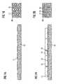
- FIG. 12diagrammatically illustrates the population of a printed circuit board 29 with active and passive circuit devices 12 , 13 .
- Active circuit components 12such as e.g. memory chips, are seated on an interposer substrate 30 provided with a connecting device 28 , e.g. solder balls on soldering pads, for the purpose of electrical contact-connection to the printed circuit board 29 .
- Passive circuit components 13such as e.g. resistors, capacitors, etc., are likewise provided on the printed circuit board 29 .
- FIG. 13shows a customary multichip module having active and passive circuit devices 12 , 13 on a printed circuit board 29 .
- the packages comprising chips 12 and interposer substrate 30are fixed e.g. by means of solder balls 28 on the module carrier 29 .
- Passive circuit devices 13are soldered onto the circuit board 29 , which have a large number of electrical connections such as conductor tracks between individual chips 12 or chips 12 and passive circuit elements 13 .
- Such a customary arrangementthus has a high total thickness of at least d1+d2+d3 in the case of only one-sided placement, which leads to a module thickness of more than 2 mm, and furthermore results in a low component density since primarily the interposer substrate and conductor tracks have a large area requirement.
- the idea on which the present invention is basedconsists essentially in all the module components, both active and passive circuit devices, being premounted on a particular mounting plane—called wafer hereinafter—, the packaging and the module assembly being combined in common process steps, and a module wafer being formed.
- this new mounting planein the form of a previous silicon wafer. This enables easier access to the required further process steps of thin-film technology (metallization, photolithography, . . . ), whose apparatuses already exist for the round wafers.
- the methodis not dependent on this form as a mounting plane. Larger rectangular areas are more effective and likewise conceivable.
- a patterned connection layeris applied to a transfer substrate, to which layer active and/or passive circuit devices with contact areas pointing toward the transfer substrate are applied to the patterned connection layer [sic] and the circuit devices are connected to one another by means of a filler at least between the circuit devices, whereupon the transfer substrate is removed and electrical connection devices for the selective contact-connection of the contact areas of the circuit devices are applied.
- ultrathin modulese.g. with 100 ⁇ m or less, on account of the use of unpackaged active circuit devices, which have a minimum of volume, weight and electrical connection planes.
- a protection deviceis applied at least over a part of the electrical connection device. As a result, the electrical connection device is mechanically protected from external influences.
- a connecting deviceis provided in regions not covered by the protection device.
- the patterned connection layeris applied in a printing process.
- the circuit devicesare arranged on the patterned connection layer in such a way that the electrical contact areas of the circuit devices are not located on the patterned connection layer.
- connection layeris not cured until after the circuit devices have been applied.
- an encapsulation of the circuit devicesis applied.
- the application of the filler and/or of the encapsulationis effected in a printing, molding (plastic injection-molding) or casting process.
- the filler and/or the encapsulationis cured in a curing process before the transfer substrate is removed.
- the electrical connection layeris provided in at least one conductive layer and has conductor tracks in the x direction and/or conductor tracks in the y direction with an interposed insulating layer given a multilayered nature, which are in each case connected to one another selectively by means of vias.
- a plurality of semiconductor circuit modulesare fabricated in a parallel process at wafer level, which modules are separated into semiconductor circuit module strips or individual semiconductor circuit modules in a subsequent process step.
- connection planecomprises a dielectric material such as a polymer, epoxy resin, adhesive, silicone or polyimide.
- the fillercomprises a non-conductive, curable material such as a polymer, adhesive or silicone.
- the encapsulationcomprises the same material as the filler or the filler has additional properties.
- the protection devicehas a passivation layer made of a non-conductive material such as a polymer.
- the semiconductor circuit modulehas at least one conductive passage from the front side to the encapsulated rear side, by means of which passage a further semiconductor circuit module can be connected, in particular by means of a conductive adhesive.
- the connecting devicehas an edge connector or soldering pads provided with solder balls.
- the semiconductor circuit modulehas a total thickness of less than 200 ⁇ m, in particular a total thickness of about 100 ⁇ m.
- FIGS. 1A , Bshow the diagrammatic illustration of a detail from an arrangement after a first method step in accordance with an embodiment of the present invention, FIG. 1A illustrating a cross section and FIG. 1B illustrating a plan view;
- FIGS. 2A , Bshow the diagrammatic illustration of a detail from an arrangement after a further method step in accordance with an embodiment of the present invention, FIG. 2A illustrating a cross section and FIG. 2B illustrating a plan view;
- FIGS. 3A , Bshow the diagrammatic illustration of a detail from an arrangement after a further method step in accordance with an embodiment of the present invention, FIG. 3B illustrating the arrangement in accordance with FIG. 3A after a directly succeeding method step;
- FIG. 4shows the diagrammatic illustration of a detail from an arrangement in the case of the method step of removal of the transfer substrate in accordance with an embodiment of the present invention
- FIG. 5shows a diagrammatic illustration of a detail from an arrangement after a further method step in accordance with an embodiment of the present invention
- FIGS. 6A , Bshow the diagrammatic illustration of a detail from an arrangement after a further method step in accordance with an embodiment of the present invention, FIG. 6A illustrating a cross section and FIG. 6B illustrating a longitudinal section (turned 90°);
- FIG. 7shows the diagrammatic illustration of a plan view for elucidating an embodiment of the present invention
- FIGS. 8A , B, Cshow the diagrammatic illustration of an arrangement for elucidating an embodiment of the present invention, FIG. 8A illustrating a plan view, FIG. 8B illustrating a cross section and FIG. 8C illustrating a longitudinal section of the arrangement;
- FIGS. 9A , Bshow the diagrammatic illustration of an arrangement in accordance with an embodiment of the present invention in longitudinal section, FIG. 9A illustrating an individual module and FIG. 9B illustrating two modules that are contact-connected to one another;
- FIGS. 10A , Bshow the diagrammatic illustration of an arrangement in accordance with an embodiment of the present invention, FIG. 10A illustrating a plan view and FIG. 10B illustrating a longitudinal section;
- FIGS. 11A , Bshow the diagrammatic illustration of an arrangement in accordance with a further embodiment of the present invention, FIG. 11A illustrating a plan view and FIG. 11B illustrating a longitudinal section;
- FIG. 12shows a diagrammatic illustration for elucidating a customary arrangement
- FIG. 13shows the diagrammatic illustration of a customary multichip arrangement
- FIGS. 14A , Bshow a flow diagram of the fabrication process for elucidating an embodiment of the present invention, FIG. 14A illustrating a conventional fabrication method and FIG. 14B illustrating a fabrication method in accordance with an embodiment of the present invention.
- FIG. 1Aillustrates a transfer substrate 10 e.g. made of glass, metal or a polymer, to which a patterned dielectric connection plane 11 is applied in a printing process.
- the dielectric connection plane 11which, at this point in time, has not yet been cured and is thus still tacky, comprises e.g. a polymer, an epoxy resin, an adhesive, silicone or a polyimide.
- FIG. 1Bshows the transfer substrate 10 with—applied thereto—individual connection areas 11 of the connection plane 11 in a plan view, the transfer substrate being embodied in rectangular fashion.
- both active and passive circuit devices 12 , 13are applied to the transfer substrate 10 and the patterned connection plane 11 .
- the circuit devices 12 , 13are applied to the connection plane in a predetermined position in such a way that the contact areas 12 ′, 13 ′ for the electrical contact-connection of the circuit devices 12 , 13 point in the direction of the transfer substrate and fall on gaps or cutouts in the patterned connection plane 11 .
- the active circuit devices 12comprise functionally checked semiconductor devices, such as e.g. memory modules, which are arranged exactly like the passive circuit devices 13 (resistors, capacitors, . . . ) e.g. in a die-bonding or pick and place process onto the uncured adhesive 11 on the transfer substrate 10 .
- the geometryi.e. the assignment of the individual circuit devices to one another, is defined in this method step.
- the components 12 , 13are arranged as near as possible to one another in order to take up a smallest possible area.
- the dielectric connection layer 11is then cured e.g. thermally or by means of UV radiation, thereby fixing the position of the circuit devices 12 , 13 with respect to one another.
- FIG. 2Bshows the plan view of a connection plane 11 provided with circuit devices 12 , 13 on the transfer substrate 10 .
- the gaps between the semiconductor devices 12 and the passive circuit devices 13are filled with a filler 14 .
- the filler 14e.g. made of a polymer, an adhesive, silicone or the like is preferably applied or introduced in a printing or casting process and then cured.
- FIG. 3Billustrates an arrangement in accordance with FIG. 3A in which an encapsulation 15 is provided over the circuit devices 12 , 13 and the gaps between the circuit devices 12 , 13 , said gaps being provided with filler 14 .
- This rear-side encapsulation 15may either be effected in the same step as the introduction of the filler 14 (in the same process device or chamber), but may also be effected afterward if the filler 14 is also intended to have additional properties which are not provided for the encapsulation 15 .
- FIG. 4illustrates the removal of the transfer substrate 10 from the cured composite comprising patterned connection plane 11 , active circuit devices 12 , passive circuit devices 13 , gaps between the circuit devices 12 , 13 , said gaps being provided with filler 14 , and the encapsulation 15 .
- the contact areas 12 ′, 13 ′ of the circuit devices 12 , 13become accessible again.
- the composite in accordance with FIG. 4is provided with an electrical connection device 16 in a process step.
- the electrical connection device 16comprises, for example, patterned, sputtered-on or electrochemically plated copper, nickel or gold conductor tracks which are applied between individual chips 12 , chips 12 and passive circuit devices 13 and/or in a manner connected to a connecting device 19 .
- the patterned conductor tracks 16run between the contact areas 12 ′, 13 ′ over the patterned dielectric connection layer 11 .
- the electrical connection device 16is preferably a double-layered line system with a dielectric layer between two patterned conductive layers, the conductive layers, one for connections or conductor tracks in the x direction, one for connections or conductor tracks in the y direction, being in electrical contact selectively by means of vias in the dielectric layer, e.g. made of polyimide.
- a dielectric layerbetween two patterned conductive layers, the conductive layers, one for connections or conductor tracks in the x direction, one for connections or conductor tracks in the y direction, being in electrical contact selectively by means of vias in the dielectric layer, e.g. made of polyimide.
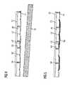
- FIG. 6Ashows the arrangement according to the invention in accordance with FIG. 5 , but with a passivation layer 17 over the electrical connection device 16 .
- the protection device 17 over the front side of the moduleswhich is applied such that it comprises a polymer e.g. in a printing process, covers the entire front side of the semiconductor circuit module 31 with the exception of a connecting device 19 or connecting contacts, illustrated in FIG. 6B .
- FIG. 6Bshows the arrangement in accordance with FIG. 6A , but not in cross section, rather in a longitudinal section (turned through 90°).
- FIG. 7illustrates a plurality of semiconductor circuit module strips 18 in a plan view which serves to illustrate rewiring devices 20 in the x direction and rewiring device 21 in the y direction as part of the electrical connection device 16 .
- FIG. 8Ashows a semiconductor circuit module strip 18 with three different sections 22 , 23 , 24 .
- the section 22represents a passivated, covered module with a passivation layer 17 , which has been omitted in the region 23 .
- the chip side walls of the embedded chipcan be seen in the section 24 , since here no electrical connection layer 16 or dielectric connection plane 11 is applied.
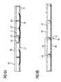
- FIG. 9Aillustrates the longitudinal section of a semiconductor memory module 31 provided with a conductive via 25 , i.e. a plated-through hole from the front side of the module to the rear side of the module.
- a conductive via 25i.e. a plated-through hole from the front side of the module to the rear side of the module.
- Such a plated-through hole 25enables, for example, the electrical linking to a second semiconductor circuit module 31 by means of an electrically conductive adhesive 26 .
- the mechanical connection between the two semiconductor circuit modules 31is preferably effected by means of an electrically non-conductive adhesive 27 in each case between the rear-side encapsulations 15 of the semiconductor circuit modules 31 .
- Such a doubly stacked module comprising two semiconductor circuit modules 31enables the component density to be increased further.
- FIGS. 10A and Bserve to illustrate a connecting device 19 in the form of a connecting strip or an edge connector.
- FIG. 11Ashows a semiconductor circuit module strip 18 with an alternative connecting device 28 with respect to FIG. 10 .
- the solder balls 28 applied to soldering padsrepresent an optimum of space saving in the x or y direction, but increase the module thickness. This results in a minimal area requirement essentially corresponding to the area of the active and passive circuit devices 12 , 13 .
- a connecting device 19 by means of connecting contacts in the form of an edge connectorcan be produced in a simple manner in the formation of the electrical connection device 16 or the rewiring device 20 , 21 if the layer applied last has a hard contact surface, for example made of gold. If such an edge connector is arranged outside the area taken up by the active and passive circuit devices 12 , 13 in an encapsulated section, then this increases the size of the module construction.
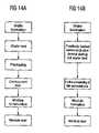
- FIG. 14Aillustrates a conventional process sequence in the fabrication of a semiconductor circuit module.
- the actual wafer fabricationis followed directly by the wafer test before chips separated individually from the wafer are housed (first level packaging).
- This packaged componenthas to be checked again in respect of its functioning before it can be used to effect a module construction with further active and passive circuit devices on a printed circuit board (second level packaging).
- a concluding module testprovides information about the functionality of the semiconductor circuit device.
- FIG. 14Billustrates a diagrammatic process sequence in accordance with an embodiment of the present invention.
- a semiconductor devicethat has been positively tested and is thus deemed to be functional
- this tested semiconductor wafer moduleis processed further [sic].
- module formationwhich has been described in detail with reference to FIGS. 1A to 6B , before such a module likewise passes through a module test.
- This process sequenceis based on knowledge of a good, i.e. tested semiconductor chip (known good die).
- module waferscan be fabricated at low cost. Vias can be integrated into the encapsulation and an electrical connection from the front side to the rear side of the substrate/module is possible. This allows these wafers to be stacked to form a three-dimensional module. If the semiconductor devices or chips and passive circuit devices are made very thin, it is possible to achieve flexible, pliant modules which can be adapted to a housing shape in a simple manner.
Landscapes
- Engineering & Computer Science (AREA)
- Microelectronics & Electronic Packaging (AREA)
- Computer Hardware Design (AREA)
- Power Engineering (AREA)
- Physics & Mathematics (AREA)
- Condensed Matter Physics & Semiconductors (AREA)
- General Physics & Mathematics (AREA)
- Manufacturing & Machinery (AREA)
- Wire Bonding (AREA)
- Encapsulation Of And Coatings For Semiconductor Or Solid State Devices (AREA)
Abstract
Description
Claims (9)
Applications Claiming Priority (1)
| Application Number | Priority Date | Filing Date | Title |
|---|---|---|---|
| DE10234951ADE10234951B4 (en) | 2002-07-31 | 2002-07-31 | Process for the production of semiconductor circuit modules |
Publications (1)
| Publication Number | Publication Date |
|---|---|
| US7074696B1true US7074696B1 (en) | 2006-07-11 |
Family
ID=30128558
Family Applications (1)
| Application Number | Title | Priority Date | Filing Date |
|---|---|---|---|
| US10/630,632Expired - Fee RelatedUS7074696B1 (en) | 2002-07-31 | 2003-07-29 | Semiconductor circuit module and method for fabricating semiconductor circuit modules |
Country Status (4)
| Country | Link |
|---|---|
| US (1) | US7074696B1 (en) |
| CN (1) | CN1235275C (en) |
| DE (1) | DE10234951B4 (en) |
| SG (1) | SG117453A1 (en) |
Cited By (22)
| Publication number | Priority date | Publication date | Assignee | Title |
|---|---|---|---|---|
| US20050067680A1 (en)* | 2003-09-30 | 2005-03-31 | Boon Suan Jeung | Castellated chip-scale packages and methods for fabricating the same |
| US20050121770A1 (en)* | 2003-12-05 | 2005-06-09 | Baek Seung D. | Wafer-level electronic modules with integral connector contacts and methods of fabricating the same |
| US20060208350A1 (en)* | 2002-06-18 | 2006-09-21 | Poo Chia Y | Support elements for semiconductor devices with peripherally located bond pads |
| US20070040259A1 (en)* | 2005-08-17 | 2007-02-22 | Chi-Hsing Hsu | Bumpless chip package |
| US7226809B2 (en) | 2002-06-18 | 2007-06-05 | Micron Technology, Inc. | Semiconductor devices and semiconductor device components with peripherally located, castellated contacts, assemblies and packages including such semiconductor devices or packages and associated methods |
| US20080273314A1 (en)* | 2007-05-04 | 2008-11-06 | Samsung Electronics Co., Ltd. | PCB having embedded IC and method for manufacturing the same |
| US20090047754A1 (en)* | 2007-08-17 | 2009-02-19 | Chipmos Technologies (Bermuda) Ltd. | Packaging method involving rearrangement of dice |
| US20100120204A1 (en)* | 2008-11-11 | 2010-05-13 | Shinko Electric Industries Co., Ltd. | Method of manufacturing semiconductor device |
| US7927922B2 (en) | 2007-12-20 | 2011-04-19 | Chipmos Technologies Inc | Dice rearrangement package structure using layout process to form a compliant configuration |
| US20120119390A1 (en)* | 2008-05-28 | 2012-05-17 | Navas Khan Oratti Kalandar | Semiconductor structure and a method of manufacturing a semiconductor structure |
| CN102915992A (en)* | 2011-08-02 | 2013-02-06 | 创意电子股份有限公司 | Semiconductor device and related method |
| US8958227B2 (en) | 2007-05-04 | 2015-02-17 | Crossfire Technologies, Inc. | Accessing or interconnecting integrated circuits |
| US9423824B2 (en) | 2011-10-03 | 2016-08-23 | Invensas Corporation | Stub minimization for multi-die wirebond assemblies with parallel windows |
| US9484080B1 (en) | 2015-11-09 | 2016-11-01 | Invensas Corporation | High-bandwidth memory application with controlled impedance loading |
| US9496243B2 (en) | 2011-10-03 | 2016-11-15 | Invensas Corporation | Microelectronic assembly with opposing microelectronic packages each having terminals with signal assignments that mirror each other with respect to a central axis |
| US9508629B2 (en) | 2011-07-12 | 2016-11-29 | Invensas Corporation | Memory module in a package |
| US9515053B2 (en) | 2011-10-03 | 2016-12-06 | Invensas Corporation | Microelectronic packaging without wirebonds to package substrate having terminals with signal assignments that mirror each other with respect to a central axis |
| US9530458B2 (en) | 2011-10-03 | 2016-12-27 | Invensas Corporation | Stub minimization using duplicate sets of signal terminals |
| US9679613B1 (en) | 2016-05-06 | 2017-06-13 | Invensas Corporation | TFD I/O partition for high-speed, high-density applications |
| US9679838B2 (en) | 2011-10-03 | 2017-06-13 | Invensas Corporation | Stub minimization for assemblies without wirebonds to package substrate |
| US9691437B2 (en) | 2014-09-25 | 2017-06-27 | Invensas Corporation | Compact microelectronic assembly having reduced spacing between controller and memory packages |
| US10090280B2 (en) | 2011-10-03 | 2018-10-02 | Invensas Corporation | Microelectronic package including microelectronic elements having stub minimization for wirebond assemblies without windows |
Families Citing this family (5)
| Publication number | Priority date | Publication date | Assignee | Title |
|---|---|---|---|---|
| US20050249945A1 (en)* | 2004-05-10 | 2005-11-10 | Wen Kun Yang | Manufacturing tool for wafer level package and method of placing dies |
| DE102004058413B4 (en)* | 2004-10-26 | 2006-10-19 | Advanced Chip Engineering Technology Inc. | Method for producing a chip-size packing structure |
| US7400037B2 (en)* | 2004-12-30 | 2008-07-15 | Advanced Chip Engineering Tachnology Inc. | Packaging structure with coplanar filling paste and dice and with patterned glue for WL-CSP |
| CN101567326B (en)* | 2008-04-24 | 2013-04-17 | 相互股份有限公司 | Printed circuit board and method of forming the same |
| US8502390B2 (en)* | 2011-07-12 | 2013-08-06 | Tessera, Inc. | De-skewed multi-die packages |
Citations (15)
| Publication number | Priority date | Publication date | Assignee | Title |
|---|---|---|---|---|
| EP0187195A2 (en) | 1984-12-28 | 1986-07-16 | Kabushiki Kaisha Toshiba | Method of manufacturing a circuit module |
| US5353195A (en)* | 1993-07-09 | 1994-10-04 | General Electric Company | Integral power and ground structure for multi-chip modules |
| US5497033A (en)* | 1993-02-08 | 1996-03-05 | Martin Marietta Corporation | Embedded substrate for integrated circuit modules |
| US5841193A (en)* | 1996-05-20 | 1998-11-24 | Epic Technologies, Inc. | Single chip modules, repairable multichip modules, and methods of fabrication thereof |
| US5937512A (en)* | 1996-01-11 | 1999-08-17 | Micron Communications, Inc. | Method of forming a circuit board |
| US6235552B1 (en)* | 1999-07-09 | 2001-05-22 | Samsung Electronics Co., Ltd. | Chip scale package and method for manufacturing the same using a redistribution substrate |
| US6239983B1 (en)* | 1995-10-13 | 2001-05-29 | Meiko Electronics Co., Ltd. | Circuit board, manufacturing method therefor, and bump-type contact head and semiconductor component packaging module using the circuit board |
| US20020036054A1 (en) | 1997-11-25 | 2002-03-28 | Seiichi Nakatani | Printed circuit board and method manufacturing the same |
| US6406942B2 (en)* | 2000-03-09 | 2002-06-18 | Nec Corporation | Flip chip type semiconductor device and method for manufacturing the same |
| US6489185B1 (en)* | 2000-09-13 | 2002-12-03 | Intel Corporation | Protective film for the fabrication of direct build-up layers on an encapsulated die package |
| US6589810B1 (en)* | 1999-04-08 | 2003-07-08 | Micron Technology, Inc. | BGA package and method of fabrication |
| US6607938B2 (en)* | 2001-07-19 | 2003-08-19 | Samsung Electronics Co., Ltd. | Wafer level stack chip package and method for manufacturing same |
| US6721469B2 (en)* | 2001-12-06 | 2004-04-13 | Chiral Photonics, Inc. | Chiral in-fiber adjustable polarizer apparatus and method |
| US6727576B2 (en)* | 2001-10-31 | 2004-04-27 | Infineon Technologies Ag | Transfer wafer level packaging |
| US6734534B1 (en)* | 2000-08-16 | 2004-05-11 | Intel Corporation | Microelectronic substrate with integrated devices |
- 2002
- 2002-07-31DEDE10234951Apatent/DE10234951B4/ennot_activeExpired - Fee Related
- 2003
- 2003-07-29USUS10/630,632patent/US7074696B1/ennot_activeExpired - Fee Related
- 2003-07-29SGSG200304194Apatent/SG117453A1/enunknown
- 2003-07-30CNCNB03152365XApatent/CN1235275C/ennot_activeExpired - Fee Related
Patent Citations (16)
| Publication number | Priority date | Publication date | Assignee | Title |
|---|---|---|---|---|
| US4635356A (en) | 1984-12-28 | 1987-01-13 | Kabushiki Kaisha Toshiba | Method of manufacturing a circuit module |
| EP0187195A2 (en) | 1984-12-28 | 1986-07-16 | Kabushiki Kaisha Toshiba | Method of manufacturing a circuit module |
| US5497033A (en)* | 1993-02-08 | 1996-03-05 | Martin Marietta Corporation | Embedded substrate for integrated circuit modules |
| US5353195A (en)* | 1993-07-09 | 1994-10-04 | General Electric Company | Integral power and ground structure for multi-chip modules |
| US6239983B1 (en)* | 1995-10-13 | 2001-05-29 | Meiko Electronics Co., Ltd. | Circuit board, manufacturing method therefor, and bump-type contact head and semiconductor component packaging module using the circuit board |
| US5937512A (en)* | 1996-01-11 | 1999-08-17 | Micron Communications, Inc. | Method of forming a circuit board |
| US5841193A (en)* | 1996-05-20 | 1998-11-24 | Epic Technologies, Inc. | Single chip modules, repairable multichip modules, and methods of fabrication thereof |
| US20020036054A1 (en) | 1997-11-25 | 2002-03-28 | Seiichi Nakatani | Printed circuit board and method manufacturing the same |
| US6589810B1 (en)* | 1999-04-08 | 2003-07-08 | Micron Technology, Inc. | BGA package and method of fabrication |
| US6235552B1 (en)* | 1999-07-09 | 2001-05-22 | Samsung Electronics Co., Ltd. | Chip scale package and method for manufacturing the same using a redistribution substrate |
| US6406942B2 (en)* | 2000-03-09 | 2002-06-18 | Nec Corporation | Flip chip type semiconductor device and method for manufacturing the same |
| US6734534B1 (en)* | 2000-08-16 | 2004-05-11 | Intel Corporation | Microelectronic substrate with integrated devices |
| US6489185B1 (en)* | 2000-09-13 | 2002-12-03 | Intel Corporation | Protective film for the fabrication of direct build-up layers on an encapsulated die package |
| US6607938B2 (en)* | 2001-07-19 | 2003-08-19 | Samsung Electronics Co., Ltd. | Wafer level stack chip package and method for manufacturing same |
| US6727576B2 (en)* | 2001-10-31 | 2004-04-27 | Infineon Technologies Ag | Transfer wafer level packaging |
| US6721469B2 (en)* | 2001-12-06 | 2004-04-13 | Chiral Photonics, Inc. | Chiral in-fiber adjustable polarizer apparatus and method |
Non-Patent Citations (1)
| Title |
|---|
| Austrian Patent Office Search Report dates Oct. 7, 2005, 6 pages. |
Cited By (43)
| Publication number | Priority date | Publication date | Assignee | Title |
|---|---|---|---|---|
| US7285850B2 (en) | 2002-06-18 | 2007-10-23 | Micron Technology, Inc. | Support elements for semiconductor devices with peripherally located bond pads |
| US20060208350A1 (en)* | 2002-06-18 | 2006-09-21 | Poo Chia Y | Support elements for semiconductor devices with peripherally located bond pads |
| US20060208351A1 (en)* | 2002-06-18 | 2006-09-21 | Poo Chia Y | Semiconductor devices including peripherally located bond pads, intermediates thereof, and assemblies and packages including the semiconductor devices |
| US7226809B2 (en) | 2002-06-18 | 2007-06-05 | Micron Technology, Inc. | Semiconductor devices and semiconductor device components with peripherally located, castellated contacts, assemblies and packages including such semiconductor devices or packages and associated methods |
| US7633159B2 (en) | 2003-09-30 | 2009-12-15 | Micron Technology, Inc. | Semiconductor device assemblies and packages with edge contacts and sacrificial substrates and other intermediate structures used or formed in fabricating the assemblies or packages |
| US20060006521A1 (en)* | 2003-09-30 | 2006-01-12 | Boon Suan J | Semiconductor device assemblies and packages with edge contacts and sacrificial substrates and other intermediate structures used or formed in fabricating the assemblies or packages |
| US8063493B2 (en) | 2003-09-30 | 2011-11-22 | Micron Technology, Inc. | Semiconductor device assemblies and packages |
| US7208335B2 (en)* | 2003-09-30 | 2007-04-24 | Micron Technology, Inc. | Castellated chip-scale packages and methods for fabricating the same |
| US20050067680A1 (en)* | 2003-09-30 | 2005-03-31 | Boon Suan Jeung | Castellated chip-scale packages and methods for fabricating the same |
| US20050121770A1 (en)* | 2003-12-05 | 2005-06-09 | Baek Seung D. | Wafer-level electronic modules with integral connector contacts and methods of fabricating the same |
| US7307340B2 (en)* | 2003-12-05 | 2007-12-11 | Samsung Electronics Co., Ltd. | Wafer-level electronic modules with integral connector contacts |
| US20070040259A1 (en)* | 2005-08-17 | 2007-02-22 | Chi-Hsing Hsu | Bumpless chip package |
| US7361982B2 (en)* | 2005-08-17 | 2008-04-22 | Via Technologies, Inc. | Bumpless chip package |
| US9449952B2 (en) | 2007-05-04 | 2016-09-20 | Crossfire Technologies, Inc. | Accessing or interconnecting integrated circuits |
| US20080273314A1 (en)* | 2007-05-04 | 2008-11-06 | Samsung Electronics Co., Ltd. | PCB having embedded IC and method for manufacturing the same |
| US8958227B2 (en) | 2007-05-04 | 2015-02-17 | Crossfire Technologies, Inc. | Accessing or interconnecting integrated circuits |
| US8629354B2 (en)* | 2007-05-04 | 2014-01-14 | Samsung Electronics Co., Ltd. | PCB having embedded IC and method for manufacturing the same |
| US9837129B2 (en) | 2007-05-04 | 2017-12-05 | Crossfire Technologies, Inc. | Accessing or interconnecting integrated circuits |
| US20090047754A1 (en)* | 2007-08-17 | 2009-02-19 | Chipmos Technologies (Bermuda) Ltd. | Packaging method involving rearrangement of dice |
| US20110163426A1 (en)* | 2007-12-20 | 2011-07-07 | Geng-Shin Shen | Dice Rearrangement Package Structure Using Layout Process to Form a Compliant Configuration |
| US7927922B2 (en) | 2007-12-20 | 2011-04-19 | Chipmos Technologies Inc | Dice rearrangement package structure using layout process to form a compliant configuration |
| US20120119390A1 (en)* | 2008-05-28 | 2012-05-17 | Navas Khan Oratti Kalandar | Semiconductor structure and a method of manufacturing a semiconductor structure |
| US8466550B2 (en)* | 2008-05-28 | 2013-06-18 | Agency For Science, Technology And Research | Semiconductor structure and a method of manufacturing a semiconductor structure |
| US8318543B2 (en)* | 2008-11-11 | 2012-11-27 | Shinko Electric Industries Co., Ltd. | Method of manufacturing semiconductor device |
| US20100120204A1 (en)* | 2008-11-11 | 2010-05-13 | Shinko Electric Industries Co., Ltd. | Method of manufacturing semiconductor device |
| US9508629B2 (en) | 2011-07-12 | 2016-11-29 | Invensas Corporation | Memory module in a package |
| US20130032937A1 (en)* | 2011-08-02 | 2013-02-07 | Taiwan Semiconductor Manufacturing Co., Ltd | Semiconductor device and associated method |
| US9053949B2 (en)* | 2011-08-02 | 2015-06-09 | Global Unichip Corporation | Semiconductor device and associated method with heat spreader having protrusion |
| CN102915992A (en)* | 2011-08-02 | 2013-02-06 | 创意电子股份有限公司 | Semiconductor device and related method |
| US9679838B2 (en) | 2011-10-03 | 2017-06-13 | Invensas Corporation | Stub minimization for assemblies without wirebonds to package substrate |
| US10032752B2 (en) | 2011-10-03 | 2018-07-24 | Invensas Corporation | Microelectronic package having stub minimization using symmetrically-positioned duplicate sets of terminals for wirebond assemblies without windows |
| US9515053B2 (en) | 2011-10-03 | 2016-12-06 | Invensas Corporation | Microelectronic packaging without wirebonds to package substrate having terminals with signal assignments that mirror each other with respect to a central axis |
| US9530458B2 (en) | 2011-10-03 | 2016-12-27 | Invensas Corporation | Stub minimization using duplicate sets of signal terminals |
| US10692842B2 (en) | 2011-10-03 | 2020-06-23 | Invensas Corporation | Microelectronic package including microelectronic elements having stub minimization for wirebond assemblies without windows |
| US9423824B2 (en) | 2011-10-03 | 2016-08-23 | Invensas Corporation | Stub minimization for multi-die wirebond assemblies with parallel windows |
| US9496243B2 (en) | 2011-10-03 | 2016-11-15 | Invensas Corporation | Microelectronic assembly with opposing microelectronic packages each having terminals with signal assignments that mirror each other with respect to a central axis |
| US10643977B2 (en) | 2011-10-03 | 2020-05-05 | Invensas Corporation | Microelectronic package having stub minimization using symmetrically-positioned duplicate sets of terminals for wirebond assemblies without windows |
| US10090280B2 (en) | 2011-10-03 | 2018-10-02 | Invensas Corporation | Microelectronic package including microelectronic elements having stub minimization for wirebond assemblies without windows |
| US9691437B2 (en) | 2014-09-25 | 2017-06-27 | Invensas Corporation | Compact microelectronic assembly having reduced spacing between controller and memory packages |
| US9484080B1 (en) | 2015-11-09 | 2016-11-01 | Invensas Corporation | High-bandwidth memory application with controlled impedance loading |
| US10026467B2 (en) | 2015-11-09 | 2018-07-17 | Invensas Corporation | High-bandwidth memory application with controlled impedance loading |
| US9928883B2 (en) | 2016-05-06 | 2018-03-27 | Invensas Corporation | TFD I/O partition for high-speed, high-density applications |
| US9679613B1 (en) | 2016-05-06 | 2017-06-13 | Invensas Corporation | TFD I/O partition for high-speed, high-density applications |
Also Published As
| Publication number | Publication date |
|---|---|
| SG117453A1 (en) | 2005-12-29 |
| CN1235275C (en) | 2006-01-04 |
| CN1477688A (en) | 2004-02-25 |
| DE10234951A1 (en) | 2004-02-12 |
| DE10234951B4 (en) | 2009-01-02 |
Similar Documents
| Publication | Publication Date | Title |
|---|---|---|
| US7074696B1 (en) | Semiconductor circuit module and method for fabricating semiconductor circuit modules | |
| US8729690B2 (en) | Assembly having stacked die mounted on substrate | |
| US7326592B2 (en) | Stacked die package | |
| US6765299B2 (en) | Semiconductor device and the method for manufacturing the same | |
| US7535109B2 (en) | Die assembly having electrical interconnect | |
| KR100692441B1 (en) | Semiconductor device and manufacturing method of semiconductor device | |
| US6815254B2 (en) | Semiconductor package with multiple sides having package contacts | |
| US9876002B2 (en) | Microelectronic package with stacked microelectronic units and method for manufacture thereof | |
| US20030230801A1 (en) | Semiconductor device assemblies and packages including multiple semiconductor devices and methods | |
| US6873040B2 (en) | Semiconductor packages for enhanced number of terminals, speed and power performance | |
| JP3999720B2 (en) | Semiconductor device and manufacturing method thereof | |
| US20070210422A1 (en) | Semiconductor package system with substrate having different bondable heights at lead finger tips | |
| KR100963471B1 (en) | Packaging Methods for Logic and Memory Integrated Circuits, Packaged Integrated Circuits and Systems | |
| US20070096249A1 (en) | Three-dimensionally integrated electronic assembly | |
| JP2002170918A (en) | Semiconductor device and its manufacturing method | |
| US6855573B2 (en) | Integrated circuit package and manufacturing method therefor with unique interconnector | |
| US6339253B1 (en) | Semiconductor package | |
| US20080029865A1 (en) | Electronic Device and Method For Producing the Same | |
| CN113725096B (en) | Semiconductor packaging method and semiconductor packaging structure | |
| JP4498336B2 (en) | Semiconductor device and manufacturing method of semiconductor device | |
| US20040089930A1 (en) | Simplified stacked chip assemblies | |
| JP3923944B2 (en) | Semiconductor device |
Legal Events
| Date | Code | Title | Description |
|---|---|---|---|
| AS | Assignment | Owner name:INFINEON TECHNOLOGIES AG, GERMANY Free format text:ASSIGNMENT OF ASSIGNORS INTEREST;ASSIGNORS:FRANKOWSKI, GERD;HEDLER, HARRY;VASQUEZ, BARBARA;REEL/FRAME:015012/0492;SIGNING DATES FROM 20031219 TO 20040204 | |
| FPAY | Fee payment | Year of fee payment:4 | |
| AS | Assignment | Owner name:QIMONDA AG, GERMANY Free format text:ASSIGNMENT OF ASSIGNORS INTEREST;ASSIGNOR:INFINEON TECHNOLOGIES AG;REEL/FRAME:023796/0001 Effective date:20060425 | |
| FPAY | Fee payment | Year of fee payment:8 | |
| AS | Assignment | Owner name:INFINEON TECHNOLOGIES AG, GERMANY Free format text:ASSIGNMENT OF ASSIGNORS INTEREST;ASSIGNOR:QIMONDA AG;REEL/FRAME:035623/0001 Effective date:20141009 | |
| AS | Assignment | Owner name:POLARIS INNOVATIONS LIMITED, IRELAND Free format text:ASSIGNMENT OF ASSIGNORS INTEREST;ASSIGNOR:INFINEON TECHNOLOGIES AG;REEL/FRAME:036818/0583 Effective date:20150708 | |
| FEPP | Fee payment procedure | Free format text:MAINTENANCE FEE REMINDER MAILED (ORIGINAL EVENT CODE: REM.) | |
| LAPS | Lapse for failure to pay maintenance fees | Free format text:PATENT EXPIRED FOR FAILURE TO PAY MAINTENANCE FEES (ORIGINAL EVENT CODE: EXP.) | |
| STCH | Information on status: patent discontinuation | Free format text:PATENT EXPIRED DUE TO NONPAYMENT OF MAINTENANCE FEES UNDER 37 CFR 1.362 | |
| FP | Lapsed due to failure to pay maintenance fee | Effective date:20180711 |