US7072996B2 - System and method of transferring data between a processing engine and a plurality of bus types using an arbiter - Google Patents
System and method of transferring data between a processing engine and a plurality of bus types using an arbiterDownload PDFInfo
- Publication number
- US7072996B2 US7072996B2US10/172,814US17281402AUS7072996B2US 7072996 B2US7072996 B2US 7072996B2US 17281402 AUS17281402 AUS 17281402AUS 7072996 B2US7072996 B2US 7072996B2
- Authority
- US
- United States
- Prior art keywords
- data
- interface
- dma
- core
- processing engine
- Prior art date
- Legal status (The legal status is an assumption and is not a legal conclusion. Google has not performed a legal analysis and makes no representation as to the accuracy of the status listed.)
- Expired - Lifetime, expires
Links
Images


Classifications
- G—PHYSICS
- G06—COMPUTING OR CALCULATING; COUNTING
- G06F—ELECTRIC DIGITAL DATA PROCESSING
- G06F13/00—Interconnection of, or transfer of information or other signals between, memories, input/output devices or central processing units
- G06F13/38—Information transfer, e.g. on bus
- G06F13/40—Bus structure
- G06F13/4004—Coupling between buses
- G06F13/4027—Coupling between buses using bus bridges
- G06F13/4031—Coupling between buses using bus bridges with arbitration
- G—PHYSICS
- G06—COMPUTING OR CALCULATING; COUNTING
- G06F—ELECTRIC DIGITAL DATA PROCESSING
- G06F13/00—Interconnection of, or transfer of information or other signals between, memories, input/output devices or central processing units
- G06F13/14—Handling requests for interconnection or transfer
- G06F13/20—Handling requests for interconnection or transfer for access to input/output bus
- G06F13/28—Handling requests for interconnection or transfer for access to input/output bus using burst mode transfer, e.g. direct memory access DMA, cycle steal
Definitions
- This inventionrelates in general to the field of electronic communications, and in particular to input/output (I/O) devices, and in one embodiment, to direct memory access (DMA) I/O devices and streaming interface I/O devices to interface with a processing core.
- I/Oinput/output
- DMAdirect memory access
- DMAdirect memory transfer access
- streaming modethe transfer of data between an I/O device and a memory unit is facilitated without the direct control of a central processing unit (CPU).
- Datacan either be transferred from memory to an I/O device (a memory source transfer) or from an I/O device to memory (a memory destination transfer).
- DMA transferstypically involve the transfer of one or more blocks of data, as data transfers of only a few bytes of data are often performed more efficiently under the direct control of the CPU.
- a streaming modeIn a streaming mode on the other hand, data is streamed directly to the device requesting the data without being stored first in a local or host memory.
- the addressing information required for a DMA interfaceis not required when operating in a streaming mode.
- DMA I/O interfacesmay include, for example, the PCI, PCI 2.0, PCI 2.1, PCI 2.2, PCIX, Infiniband by Intel, and HyperTransport.
- Streaming interfacesmay include, for example, the Packet-Over-SONET Physical-Layer Three (POS-PHY3) referred to as a PL3 interface, SPI 4, and GMII as well as other packet interfaces.
- POS-PHY3Packet-Over-SONET Physical-Layer Three
- SPI 4Packet-Over-SONET Physical-Layer Three
- GMIIPacket-Over-SONET Physical-Layer Three
- datais retrieved from DMA-type interfaces while data is pushed from streaming-type interfaces.
- processing cores and their associated support systemsare generally designed specifically for interfacing with one particular type of interface. This unfortunately requires a significant redesign of a processing core for each type of interface, which among other things, increases costs as well as increases time-to-market.
- the present inventionprovides, among other things, an input/output (I/O) system that transfers control and data between a core-processing engine and a plurality of bus types including a direct memory access (DMA) bus and a streaming data bus.
- the systemcomprises a streaming interface for transferring streamed data from the streaming data bus to the core-processing engine, a DMA interface for transferring DMA data from the DMA data bus to the core-processing engine, and an arbiter for coordinating data transfer with the core-processing engine between the streaming interface and DMA interface.
- I/Oinput/output
- DMAdirect memory access
- the systemcomprises a streaming interface for transferring streamed data from the streaming data bus to the core-processing engine, a DMA interface for transferring DMA data from the DMA data bus to the core-processing engine, and an arbiter for coordinating data transfer with the core-processing engine between the streaming interface and DMA interface.
- an arbiterreceives a request to process data from the core-processing engine indicating when the core-processing engine is ready to process data, selects either the streaming interface or the DMA interface, enters into an address phase with the core-processing engine, and enters into a data phase with the core-processing engine to transfer data from the selected interface to the core-processing engine.
- a dummy addressmay be used for a host source address for reading data.
- a dummy addressmay be used as a host destination address when writing data.
- the arbitermay operate in a split-bus-type mode performing the address phase for one or more channels of a plurality of channels prior to entering into a data phase for one of the channels. In one embodiment, several address phases are performed before the first data phase is performed.
- the present inventionprovides a method of transferring control and data between a core-processing engine and a plurality of bus types including a DMA bus and a streaming data bus.
- the methodmay comprise transferring streamed data from the streaming data bus to the core-processing engine using a streaming interface, transferring DMA data from the DMA data bus to the core-processing engine using a DMA interface, and coordinating data transfer with the core-processing engine between the streaming interface and DMA interface using an arbiter.
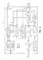
- FIG. 1is a simplified functional block diagram of a system architecture configuration in which an embodiment of the present invention may be practiced
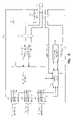
- FIG. 2is a simplified functional block diagram of flexible I/O system in accordance with an embodiment of the present invention
- FIG. 3is a simplified functional block diagram of DMA interface in accordance with an embodiment of the present invention.
- FIG. 4is a simplified functional block diagram of streaming interface in accordance with an embodiment of the present invention.
- FIG. 5is a simplified functional block diagram of an arbiter in accordance with an embodiment of the present invention.
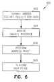
- FIG. 6is a simplified flow chart of a control and data transfer procedure in accordance with an embodiment of the present invention.
- the present inventionprovides, among other things a flexible input/output (I/O) interface that allows a processing core to communicate high-speed data with a several different types of interfaces including a Direct Memory Access (DMA) interface and a streaming interface.
- the flexible I/Omay also provide a common bus interface to the processing core and may allow the processing core to interface with any type of streaming and DMA type interfaces without redesign.
- FIG. 1is a simplified functional block diagram of a system architecture configuration in which an embodiment of the present invention may be practiced.
- System configuration 100may include processing core 102 to receive data for processing from a plurality of busses 108 , 110 , 112 through flexible I/O system 106 .
- processing core 102may receive data through flexible I/O system 106 in a streamed mode over bus 108
- processing core 102may receive data through flexible I/O system 106 in a DMA mode over bus 110 .
- processing core 102may also provide data to bus 108 through flexible I/O system 106 in a streamed mode, and may provide data to bus 110 through flexible I/O system 106 in a DMA mode.
- bus 110may be configured to communicate data in accordance with, for example, PCI, PCI 2.0, PCI 2.1, PCI 2.2, PCIX, Infiniband by Intel, and/or HyperTransport DMA interface standard. Other DMA configurations may also be suitable for bus 110 .
- bus 108may be configured to communicate data in accordance with, for example, the Packet-Over-SONIET Physical-Layer Three (POS-PHY3) referred to as a PL3 interface, SPI 4, and GMII as well as other packet interfaces.
- POS-PHY3Packet-Over-SONIET Physical-Layer Three
- Other streaming data configurationsmay also be suitable for bus 108 .
- Other data busses 112may be configured to communicate DMA and/or streaming data, and in one embodiment, may include up to ten or even a hundred or more of other busses 112 .
- Flexible I/O system 106may arbitrate between data transferred over the several busses, and may perform any protocols to interface with each of the busses and with processing core 102 .
- system 106may provide a common bus interface 104 for processing core 102 allowing processing core 102 to communicate differing types of data over a plurality of bus types that implement different bus protocols and/or standards.
- processing core 102may be a processing engine, such as a crypto processing core (e.g., crypto engine) that processes blocks of data of a predetermined size.
- processing core 102may process data in a pipelined manner.
- processor core 102may process data in accordance with a plurality of processing threads (i.e., channels).
- flexible I/O system 106 and processing core 102may be fabricated on a single semiconductor chip.
- FIG. 2is a simplified functional block diagram of flexible I/O system in accordance with an embodiment of the present invention.
- Flexible I/O system 200may suitable for use as flexible I/O system 106 ( FIG. 1 ) although I/O systems may also be suitable.
- Flexible I/O system 200may comprise streaming-type interface 207 for communicating streamed data through streaming I/O core 208 , for example, over a streaming data bus such as bus 108 ( FIG. 1 ).
- Flexible I/O system 200may also comprise DMA-type interface 209 for communicating DMA data through DMA I/O core 210 over a DMA data bus, such as bus 110 ( FIG. 1 ).
- flexible I/O system 200may also comprise other interfaces 211 for communicating other data through other I/O cores 212 over other data buses, such as other busses 112 ( FIG. 1 ).
- Other interfaces 211may include interfaces for communicating DMA and/or streamed data.
- Embodiments of the present inventionprovide for several other interfaces 212 and may provide for up to ten or even a hundred or more other interfaces 211 .
- I/O cores 208 , 210 and 212may be state machines that implement a bus protocol in accordance with their associated bus.
- interfaces 207 , 209 and 211may share a common address bus and common data bus 204 coupled to processing core 102 ( FIG. 1 ).
- Interfaces 207 , 209 and 211may also have separate control signal busses, respectively control signal buses 218 , 220 and 222 , which couple with I/O arbiter 202 .
- Arbiter 202may arbitrate between the interfaces and may provide a common interface 203 for processing core 102 ( FIG. 1 ).
- interfaces 207 , 209 and 211may not have to share a common address bus and common data bus, such as bus 204 .
- interfaces 207 , 209 and 211may each have their own address bus and may each have their own data bus coupled to processing core 102 ( FIG. 1 ) through, for example, a switching fabric.
- This configurationmay allow for parallel (rather than serial) communications of each channel of the processing core with any of the I/O interfaces.
- This embodimentmay include, for example, a set of source and destination address and data busses for each channel.
- FIG. 3is a simplified functional block diagram of DMA interface in accordance with an embodiment of the present invention.
- DMA interface 300is an example of a DMA interface that may be suitable for use as DMA interface 209 ( FIG. 2 ) although other interfaces may also be suitable.
- Address generator and interface logic element 302converts address requests and may include logic for interfacing with DMA I/O core 210 . Addresses for each of the channels for which processing core processes data may be coordinated by element 302 .
- Read and write request arbiter 308may operate during addressing phases of a DMA data transfer and may be responsive to read and write request signals provided by arbiter 202 ( FIG. 2 ). Read and write request arbiter 308 may generate read and write grant signals.
- FIFO's 310 and 312may buffer the addresses. Data may be transferred through the use of write unloading interface 304 , read loading interface 306 , write FIFO 314 , read FIFO 316 , write loading interface 320 and read unloading interface 318 .
- Interfaces 304 and 306maybe state machines implementing a particular DMA data transfer, such as required for PCI busses. Interfaces 318 and 320 may support both big and little Endian standards, as determined by configuration bits set by a host.
- bus 322may be a common address and data bus coupled with a processing core and may be shared with other interfaces. In another embodiment, bus 322 may be a non-common address bus and/or a non-common data bus coupled with a processing core through a switching fabric allowing interface 300 to access any channel of the processing core in parallel with other interfaces.
- a DMA transferis typically accomplished in the following manner.
- the processing unitinitializes both the DMA interface and the I/O device by indicating, for example, a source address, a destination address, and the amount of data to be transferred.
- the address and control signals to control the I/O busare generated to perform successive data transfers until all of the requested data have been transferred from the source to the destination.
- the sourceresponds to the address and control signals generated by the DMA interface to transmit the requested data
- the destinationresponds to the address and control signals generated by the DMA interface to receive the data.
- the DMA interfacemay notify the processing unit of this condition by activating an interrupt.
- the arbitermay operate in a split-bus-type mode performing the address phase for one or more channels of a plurality of channels prior to entering into a data phase for one of the channels.
- several address phasesare performed before the first data phase is performed.
- address phasesmay be performed independent of data phases allowing for improved throughput. This may allow for several channels to be queued up depending on the latency of the I/O device until, for example, data for a particular channel is ready.
- FIG. 4is a simplified functional block diagram of streaming interface in accordance with an embodiment of the present invention.
- Streaming interface 400is one example of a streaming interface suitable for use as streaming interface 207 ( FIG. 2 ) although other interfaces may also be suitable.
- Streaming interface 400includes transmit/receive request presenter element 402 to coordinate requests for streamed data.
- Element 403may include logic for interfacing with streaming interface core 208 ( FIG. 2 ).
- Read and write request arbiter 408may be responsive to read and write request signals provided by arbiter 202 ( FIG. 2 ) and may inform the arbiter when streaming data is ready. Read and write request arbiter 408 may generate read and write grant signals.
- FIFO's 410 and 412may buffer addresses, including dummy addresses, and are operable for performing an address phase with the processing core. Since streamed data does not require full addressing for the host like DMA data, dummy addresses may be used. In one embodiment when the streaming interface 400 is selected and during the addressing phase, a dummy address may be used for a host source address for reading data, and a dummy address may be used as a host destination address when writing data.
- Streamed datamay be transferred through the use of write unloading interface 404 , read loading interface 406 , write FIFO 414 , read FIFO 416 , write loading interface 420 and read unloading interface 418 .
- Interfaces 404 and 406may be state machines implementing the transfer of streamed data in accordance with any streamed data protocol, such as, for example, the PL3 standard protocol.
- interfaces 418 and 420may support both big and little Endian standards, determined by configuration bits set by the host.
- bus 422may be a common address and data bus coupled with a processing core and may be shared with other interfaces.
- bus 422may be a non-common address bus and/or a non-common data bus coupled with a processing core through a switching fabric allowing interface 400 to access any channel of the processing core in parallel with other interfaces.
- FIG. 5is a simplified functional block diagram of an arbiter in accordance with an embodiment of the present invention.
- Arbiter 500may be suitable for use as arbiter 202 ( FIG. 2 ) although other devices may also be suitable.
- Arbiter 500comprises multiplexing element 502 to multiplex signals between a processing core and a plurality of interfaces.
- Programmable register 506may be programmed by a host and may stores information for identifying which of channel of a plurality of channels may be associated with a particular type of interface.
- Control logic 504may coordinate the operation of multiplexing element 502 in response to information in register 506 , signals provided by the processing engine and signals provided by the interfaces.
- the hostmay dynamically reconfigure channels by updating the channel information bits contained in register 506 .
- processing core 102may include elements for processing up to eight channels (e.g., eight multiple parallel processing threads) to achieve a higher throughput.
- processing core 102may support signals lines 505 for each channel.
- processing core 102may include read and write request and grant signal lines for each supported channel. The operation of arbiter 500 within system 200 ( FIG. 2 ) is described in more detail below.
- FIG. 6is a simplified flow chart of a control and data transfer procedure in accordance with an embodiment of the present invention.
- Procedure 600may be performed by arbiter 500 ( FIG. 5 ) although other device may also be suitable.
- the processing coremay generate a request, which may be received by an arbiter.
- the requestmay indicate the processing core is ready to process data or that processed data is available.
- the requestmay also indicate a particular channel and may be received on a request signal line for that particular channel.
- the arbitermay select an interface for the data transfer by determining whether the available interface matches the channel type (e.g., DMA or streaming) and whether the interface has data available or is ready to accept data.
- the channel typee.g., DMA or streaming
- an address phase of the data transferis performed.
- the arbitermay coordinate the address phase between the selected interface and the processing core.
- a dummy addressmay be used for a host source address for reading data.
- a dummy addressmay also be used as a host destination address when writing data.
- a data phase of the data transferis performed wherein data is transferred between the processing core over a bus associated with the selected interface.
- the arbitermay operate in a split-bus-type mode performing the address phase for one or more channels of a plurality of channels prior to entering into a data phase for one of the channels.
- several address phasesare performed before the first data phase is performed.
- the system and methodmay reduce design costs and time-to-market.
- the system and methoduse a flexible interface for streamed and DMA data.
- a common bus interfaceis provided for a processing core allowing for the transfer of both streaming and DMA data. This allows the processing core to communicate high-speed data with a several different types of interfaces including DMA interfaces and streaming interfaces.
Landscapes
- Engineering & Computer Science (AREA)
- Theoretical Computer Science (AREA)
- General Engineering & Computer Science (AREA)
- Physics & Mathematics (AREA)
- General Physics & Mathematics (AREA)
- Computer Hardware Design (AREA)
- Bus Control (AREA)
- Information Transfer Systems (AREA)
Abstract
Description
Claims (25)
Priority Applications (3)
| Application Number | Priority Date | Filing Date | Title |
|---|---|---|---|
| US10/172,814US7072996B2 (en) | 2001-06-13 | 2002-06-12 | System and method of transferring data between a processing engine and a plurality of bus types using an arbiter |
| PCT/US2002/018681WO2002101566A2 (en) | 2001-06-13 | 2002-06-13 | Flexible i/o interface and method for providing a common interface to a processing core |
| AU2002345660AAU2002345660A1 (en) | 2001-06-13 | 2002-06-13 | Flexible i/o interface and method for providing a common interface to a processing core |
Applications Claiming Priority (2)
| Application Number | Priority Date | Filing Date | Title |
|---|---|---|---|
| US29797501P | 2001-06-13 | 2001-06-13 | |
| US10/172,814US7072996B2 (en) | 2001-06-13 | 2002-06-12 | System and method of transferring data between a processing engine and a plurality of bus types using an arbiter |
Publications (2)
| Publication Number | Publication Date |
|---|---|
| US20030126319A1 US20030126319A1 (en) | 2003-07-03 |
| US7072996B2true US7072996B2 (en) | 2006-07-04 |
Family
ID=26868485
Family Applications (1)
| Application Number | Title | Priority Date | Filing Date |
|---|---|---|---|
| US10/172,814Expired - LifetimeUS7072996B2 (en) | 2001-06-13 | 2002-06-12 | System and method of transferring data between a processing engine and a plurality of bus types using an arbiter |
Country Status (3)
| Country | Link |
|---|---|
| US (1) | US7072996B2 (en) |
| AU (1) | AU2002345660A1 (en) |
| WO (1) | WO2002101566A2 (en) |
Cited By (29)
| Publication number | Priority date | Publication date | Assignee | Title |
|---|---|---|---|---|
| US20040017813A1 (en)* | 2002-05-15 | 2004-01-29 | Manu Gulati | Transmitting data from a plurality of virtual channels via a multiple processor device |
| US20060184710A1 (en)* | 2005-02-17 | 2006-08-17 | Nokia Inc. | Bridge between a single channel high speed bus and a multiple channel low speed bus |
| US20070028152A1 (en)* | 2005-08-01 | 2007-02-01 | Mishra Kishore K | System and Method of Processing Received Line Traffic for PCI Express that Provides Line-Speed Processing, and Provides Substantial Gate-Count Savings |
| US20090109996A1 (en)* | 2007-10-29 | 2009-04-30 | Hoover Russell D | Network on Chip |
| US20090125706A1 (en)* | 2007-11-08 | 2009-05-14 | Hoover Russell D | Software Pipelining on a Network on Chip |
| US20090125574A1 (en)* | 2007-11-12 | 2009-05-14 | Mejdrich Eric O | Software Pipelining On a Network On Chip |
| US20090125703A1 (en)* | 2007-11-09 | 2009-05-14 | Mejdrich Eric O | Context Switching on a Network On Chip |
| US20090135739A1 (en)* | 2007-11-27 | 2009-05-28 | Hoover Russell D | Network On Chip With Partitions |
| US20090182954A1 (en)* | 2008-01-11 | 2009-07-16 | Mejdrich Eric O | Network on Chip That Maintains Cache Coherency with Invalidation Messages |
| US20090187716A1 (en)* | 2008-01-17 | 2009-07-23 | Miguel Comparan | Network On Chip that Maintains Cache Coherency with Invalidate Commands |
| US20090210883A1 (en)* | 2008-02-15 | 2009-08-20 | International Business Machines Corporation | Network On Chip Low Latency, High Bandwidth Application Messaging Interconnect |
| US20090245257A1 (en)* | 2008-04-01 | 2009-10-01 | International Business Machines Corporation | Network On Chip |
| US20090260013A1 (en)* | 2008-04-14 | 2009-10-15 | International Business Machines Corporation | Computer Processors With Plural, Pipelined Hardware Threads Of Execution |
| US20090259789A1 (en)* | 2005-08-22 | 2009-10-15 | Shuhei Kato | Multi-processor, direct memory access controller, and serial data transmitting/receiving apparatus |
| US20090271597A1 (en)* | 2008-04-24 | 2009-10-29 | International Business Machines Corporations | Branch Prediction In A Computer Processor |
| US20090282214A1 (en)* | 2008-05-09 | 2009-11-12 | International Business Machines Corporation | Network On Chip With Low Latency, High Bandwidth Application Messaging Interconnects That Abstract Hardware Inter-Thread Data Communications Into An Architected State of A Processor |
| US20090282227A1 (en)* | 2008-05-09 | 2009-11-12 | International Business Machines Corporation | Monitoring Software Pipeline Performance On A Network On Chip |
| US20090282139A1 (en)* | 2008-05-09 | 2009-11-12 | International Business Machines Corporation | Emulating A Computer Run Time Environment |
| US20090282197A1 (en)* | 2008-05-09 | 2009-11-12 | International Business Machines Corporation | Network On Chip |
| US20090282226A1 (en)* | 2008-05-09 | 2009-11-12 | International Business Machines Corporation | Context Switching On A Network On Chip |
| US20090282222A1 (en)* | 2008-05-09 | 2009-11-12 | International Business Machines Corporation | Dynamic Virtual Software Pipelining On A Network On Chip |
| US20090287885A1 (en)* | 2008-05-15 | 2009-11-19 | International Business Machines Corporation | Administering Non-Cacheable Memory Load Instructions |
| US20090307714A1 (en)* | 2008-06-09 | 2009-12-10 | International Business Machines Corporation | Network on chip with an i/o accelerator |
| US8018466B2 (en) | 2008-02-12 | 2011-09-13 | International Business Machines Corporation | Graphics rendering on a network on chip |
| US8040799B2 (en) | 2008-05-15 | 2011-10-18 | International Business Machines Corporation | Network on chip with minimum guaranteed bandwidth for virtual communications channels |
| US8195884B2 (en) | 2008-09-18 | 2012-06-05 | International Business Machines Corporation | Network on chip with caching restrictions for pages of computer memory |
| US8423715B2 (en) | 2008-05-01 | 2013-04-16 | International Business Machines Corporation | Memory management among levels of cache in a memory hierarchy |
| US8700873B2 (en) | 2010-10-14 | 2014-04-15 | International Business Machines Corporation | Direct memory access memory management |
| US20210389741A1 (en)* | 2018-11-19 | 2021-12-16 | Omron Corporation | Control system and control device |
Families Citing this family (12)
| Publication number | Priority date | Publication date | Assignee | Title |
|---|---|---|---|---|
| CN1296844C (en)* | 2003-06-20 | 2007-01-24 | 上海奇码数字信息有限公司 | Data transmission method and data transmission system |
| US20060010260A1 (en)* | 2004-07-07 | 2006-01-12 | Fung Hon C | Direct memory access (DMA) controller and bus structure in a master/slave system |
| US8054857B2 (en) | 2004-10-07 | 2011-11-08 | Lsi Corporation | Task queuing methods and systems for transmitting frame information over an I/O interface |
| JP2007052501A (en)* | 2005-08-15 | 2007-03-01 | Canon Inc | Communication control apparatus, communication control method, exposure apparatus, and device manufacturing method |
| US8495020B1 (en)* | 2007-06-27 | 2013-07-23 | ENORCOM Corporation | Mobile information system |
| US8700821B2 (en)* | 2008-08-22 | 2014-04-15 | Intel Corporation | Unified multi-transport medium connector architecture |
| US9697159B2 (en)* | 2011-12-27 | 2017-07-04 | Intel Corporation | Multi-protocol I/O interconnect time synchronization |
| US8953644B2 (en) | 2011-12-27 | 2015-02-10 | Intel Corporation | Multi-protocol I/O interconnect time synchronization |
| US8775713B2 (en) | 2011-12-27 | 2014-07-08 | Intel Corporation | Multi-protocol tunneling over an I/O interconnect |
| US8782321B2 (en)* | 2012-02-08 | 2014-07-15 | Intel Corporation | PCI express tunneling over a multi-protocol I/O interconnect |
| US8880923B2 (en) | 2012-03-29 | 2014-11-04 | Intel Corporation | Link power management in an I/O interconnect |
| US12430673B2 (en)* | 2022-05-23 | 2025-09-30 | Verizon Patent And Licensing Inc. | Systems and methods for request validation |
Citations (20)
| Publication number | Priority date | Publication date | Assignee | Title |
|---|---|---|---|---|
| US5546547A (en)* | 1994-01-28 | 1996-08-13 | Apple Computer, Inc. | Memory bus arbiter for a computer system having a dsp co-processor |
| US5566306A (en) | 1992-06-11 | 1996-10-15 | Seiko Epson Corporation | Transfer control apparatus for independent transfer of data from a storage device to an I/O device over a secondary bus |
| US5828856A (en)* | 1994-01-28 | 1998-10-27 | Apple Computer, Inc. | Dual bus concurrent multi-channel direct memory access controller and method |
| US5870570A (en) | 1996-10-29 | 1999-02-09 | Vlsi Technology, Inc. | Multiple bus agent integrated circuit device for connecting to an external bus |
| US5872936A (en)* | 1995-05-08 | 1999-02-16 | Apple Computer, Inc. | Apparatus for and method of arbitrating bus conflicts |
| US5878217A (en) | 1994-11-21 | 1999-03-02 | Cirrus Logic, Inc. | Network controller for switching into DMA mode based on anticipated memory overflow and out of DMA mode when the host processor is available |
| US6134625A (en) | 1998-02-18 | 2000-10-17 | Intel Corporation | Method and apparatus for providing arbitration between multiple data streams |
| US6195722B1 (en)* | 1998-01-26 | 2001-02-27 | Intel Corporation | Method and apparatus for deferring transactions on a host bus having a third party agent |
| US6205524B1 (en)* | 1998-09-16 | 2001-03-20 | Neomagic Corp. | Multimedia arbiter and method using fixed round-robin slots for real-time agents and a timed priority slot for non-real-time agents |
| US6272582B1 (en)* | 1998-02-20 | 2001-08-07 | Mitsubishi Denki Kabushiki Kaisha | PCI-PCI bridge allowing controlling of a plurality of PCI agents including a VGA device |
| US6275491B1 (en)* | 1997-06-03 | 2001-08-14 | Texas Instruments Incorporated | Programmable architecture fast packet switch |
| US6434645B1 (en)* | 1998-05-20 | 2002-08-13 | Creative Technology, Ltd | Methods and apparatuses for managing multiple direct memory access channels |
| US6487628B1 (en)* | 1999-03-31 | 2002-11-26 | Compaq Computer Corporation | Peripheral component interface with multiple data channels and reduced latency over a system area network |
| US6556580B1 (en)* | 1999-12-16 | 2003-04-29 | 3Com Corporation | Multi-function transmit packet buffer |
| US6608625B1 (en)* | 1998-10-14 | 2003-08-19 | Hitachi, Ltd. | Three dimensional graphic processor |
| US6636915B1 (en)* | 1999-05-19 | 2003-10-21 | Eci Telecom Ltd. | Cell bus distributed arbitration system and method |
| US6651122B2 (en)* | 2000-12-07 | 2003-11-18 | Micron Technology, Inc. | Method of detecting a source strobe event using change detection |
| US6684296B2 (en)* | 2001-05-18 | 2004-01-27 | Broadcom Corporation | Source controlled cache allocation |
| US6728808B1 (en)* | 2000-02-07 | 2004-04-27 | 3Com Corporation | Mechanism for optimizing transaction retries within a system utilizing a PCI bus architecture |
| US6785230B1 (en)* | 1999-05-25 | 2004-08-31 | Matsushita Electric Industrial Co., Ltd. | Audio transmission apparatus |
- 2002
- 2002-06-12USUS10/172,814patent/US7072996B2/ennot_activeExpired - Lifetime
- 2002-06-13WOPCT/US2002/018681patent/WO2002101566A2/ennot_activeApplication Discontinuation
- 2002-06-13AUAU2002345660Apatent/AU2002345660A1/ennot_activeAbandoned
Patent Citations (20)
| Publication number | Priority date | Publication date | Assignee | Title |
|---|---|---|---|---|
| US5566306A (en) | 1992-06-11 | 1996-10-15 | Seiko Epson Corporation | Transfer control apparatus for independent transfer of data from a storage device to an I/O device over a secondary bus |
| US5546547A (en)* | 1994-01-28 | 1996-08-13 | Apple Computer, Inc. | Memory bus arbiter for a computer system having a dsp co-processor |
| US5828856A (en)* | 1994-01-28 | 1998-10-27 | Apple Computer, Inc. | Dual bus concurrent multi-channel direct memory access controller and method |
| US5878217A (en) | 1994-11-21 | 1999-03-02 | Cirrus Logic, Inc. | Network controller for switching into DMA mode based on anticipated memory overflow and out of DMA mode when the host processor is available |
| US5872936A (en)* | 1995-05-08 | 1999-02-16 | Apple Computer, Inc. | Apparatus for and method of arbitrating bus conflicts |
| US5870570A (en) | 1996-10-29 | 1999-02-09 | Vlsi Technology, Inc. | Multiple bus agent integrated circuit device for connecting to an external bus |
| US6275491B1 (en)* | 1997-06-03 | 2001-08-14 | Texas Instruments Incorporated | Programmable architecture fast packet switch |
| US6195722B1 (en)* | 1998-01-26 | 2001-02-27 | Intel Corporation | Method and apparatus for deferring transactions on a host bus having a third party agent |
| US6134625A (en) | 1998-02-18 | 2000-10-17 | Intel Corporation | Method and apparatus for providing arbitration between multiple data streams |
| US6272582B1 (en)* | 1998-02-20 | 2001-08-07 | Mitsubishi Denki Kabushiki Kaisha | PCI-PCI bridge allowing controlling of a plurality of PCI agents including a VGA device |
| US6434645B1 (en)* | 1998-05-20 | 2002-08-13 | Creative Technology, Ltd | Methods and apparatuses for managing multiple direct memory access channels |
| US6205524B1 (en)* | 1998-09-16 | 2001-03-20 | Neomagic Corp. | Multimedia arbiter and method using fixed round-robin slots for real-time agents and a timed priority slot for non-real-time agents |
| US6608625B1 (en)* | 1998-10-14 | 2003-08-19 | Hitachi, Ltd. | Three dimensional graphic processor |
| US6487628B1 (en)* | 1999-03-31 | 2002-11-26 | Compaq Computer Corporation | Peripheral component interface with multiple data channels and reduced latency over a system area network |
| US6636915B1 (en)* | 1999-05-19 | 2003-10-21 | Eci Telecom Ltd. | Cell bus distributed arbitration system and method |
| US6785230B1 (en)* | 1999-05-25 | 2004-08-31 | Matsushita Electric Industrial Co., Ltd. | Audio transmission apparatus |
| US6556580B1 (en)* | 1999-12-16 | 2003-04-29 | 3Com Corporation | Multi-function transmit packet buffer |
| US6728808B1 (en)* | 2000-02-07 | 2004-04-27 | 3Com Corporation | Mechanism for optimizing transaction retries within a system utilizing a PCI bus architecture |
| US6651122B2 (en)* | 2000-12-07 | 2003-11-18 | Micron Technology, Inc. | Method of detecting a source strobe event using change detection |
| US6684296B2 (en)* | 2001-05-18 | 2004-01-27 | Broadcom Corporation | Source controlled cache allocation |
Non-Patent Citations (2)
| Title |
|---|
| IBM Technical Disclosure Bulletin, Apr. 1995, US, Title: "Micro Channel Architecutre for Real-Time Multimedia", TDB-ACC-NO: NN9504535.* |
| International Search Report for corresponding PCT application No. PCT/US02/18681. |
Cited By (46)
| Publication number | Priority date | Publication date | Assignee | Title |
|---|---|---|---|---|
| US20040017813A1 (en)* | 2002-05-15 | 2004-01-29 | Manu Gulati | Transmitting data from a plurality of virtual channels via a multiple processor device |
| US20060184710A1 (en)* | 2005-02-17 | 2006-08-17 | Nokia Inc. | Bridge between a single channel high speed bus and a multiple channel low speed bus |
| US20070028152A1 (en)* | 2005-08-01 | 2007-02-01 | Mishra Kishore K | System and Method of Processing Received Line Traffic for PCI Express that Provides Line-Speed Processing, and Provides Substantial Gate-Count Savings |
| US20090259789A1 (en)* | 2005-08-22 | 2009-10-15 | Shuhei Kato | Multi-processor, direct memory access controller, and serial data transmitting/receiving apparatus |
| US20090109996A1 (en)* | 2007-10-29 | 2009-04-30 | Hoover Russell D | Network on Chip |
| US20090125706A1 (en)* | 2007-11-08 | 2009-05-14 | Hoover Russell D | Software Pipelining on a Network on Chip |
| US20090125703A1 (en)* | 2007-11-09 | 2009-05-14 | Mejdrich Eric O | Context Switching on a Network On Chip |
| US8898396B2 (en) | 2007-11-12 | 2014-11-25 | International Business Machines Corporation | Software pipelining on a network on chip |
| US20090125574A1 (en)* | 2007-11-12 | 2009-05-14 | Mejdrich Eric O | Software Pipelining On a Network On Chip |
| US8261025B2 (en) | 2007-11-12 | 2012-09-04 | International Business Machines Corporation | Software pipelining on a network on chip |
| US20090135739A1 (en)* | 2007-11-27 | 2009-05-28 | Hoover Russell D | Network On Chip With Partitions |
| US8526422B2 (en) | 2007-11-27 | 2013-09-03 | International Business Machines Corporation | Network on chip with partitions |
| US20090182954A1 (en)* | 2008-01-11 | 2009-07-16 | Mejdrich Eric O | Network on Chip That Maintains Cache Coherency with Invalidation Messages |
| US8473667B2 (en) | 2008-01-11 | 2013-06-25 | International Business Machines Corporation | Network on chip that maintains cache coherency with invalidation messages |
| US20090187716A1 (en)* | 2008-01-17 | 2009-07-23 | Miguel Comparan | Network On Chip that Maintains Cache Coherency with Invalidate Commands |
| US8010750B2 (en) | 2008-01-17 | 2011-08-30 | International Business Machines Corporation | Network on chip that maintains cache coherency with invalidate commands |
| US8018466B2 (en) | 2008-02-12 | 2011-09-13 | International Business Machines Corporation | Graphics rendering on a network on chip |
| US20090210883A1 (en)* | 2008-02-15 | 2009-08-20 | International Business Machines Corporation | Network On Chip Low Latency, High Bandwidth Application Messaging Interconnect |
| US8490110B2 (en) | 2008-02-15 | 2013-07-16 | International Business Machines Corporation | Network on chip with a low latency, high bandwidth application messaging interconnect |
| US20090245257A1 (en)* | 2008-04-01 | 2009-10-01 | International Business Machines Corporation | Network On Chip |
| US20090260013A1 (en)* | 2008-04-14 | 2009-10-15 | International Business Machines Corporation | Computer Processors With Plural, Pipelined Hardware Threads Of Execution |
| US8078850B2 (en) | 2008-04-24 | 2011-12-13 | International Business Machines Corporation | Branch prediction technique using instruction for resetting result table pointer |
| US20090271597A1 (en)* | 2008-04-24 | 2009-10-29 | International Business Machines Corporations | Branch Prediction In A Computer Processor |
| US8843706B2 (en) | 2008-05-01 | 2014-09-23 | International Business Machines Corporation | Memory management among levels of cache in a memory hierarchy |
| US8423715B2 (en) | 2008-05-01 | 2013-04-16 | International Business Machines Corporation | Memory management among levels of cache in a memory hierarchy |
| US20090282214A1 (en)* | 2008-05-09 | 2009-11-12 | International Business Machines Corporation | Network On Chip With Low Latency, High Bandwidth Application Messaging Interconnects That Abstract Hardware Inter-Thread Data Communications Into An Architected State of A Processor |
| US7991978B2 (en) | 2008-05-09 | 2011-08-02 | International Business Machines Corporation | Network on chip with low latency, high bandwidth application messaging interconnects that abstract hardware inter-thread data communications into an architected state of a processor |
| US8020168B2 (en) | 2008-05-09 | 2011-09-13 | International Business Machines Corporation | Dynamic virtual software pipelining on a network on chip |
| US8494833B2 (en) | 2008-05-09 | 2013-07-23 | International Business Machines Corporation | Emulating a computer run time environment |
| US20090282226A1 (en)* | 2008-05-09 | 2009-11-12 | International Business Machines Corporation | Context Switching On A Network On Chip |
| US20090282222A1 (en)* | 2008-05-09 | 2009-11-12 | International Business Machines Corporation | Dynamic Virtual Software Pipelining On A Network On Chip |
| US8214845B2 (en) | 2008-05-09 | 2012-07-03 | International Business Machines Corporation | Context switching in a network on chip by thread saving and restoring pointers to memory arrays containing valid message data |
| US20090282227A1 (en)* | 2008-05-09 | 2009-11-12 | International Business Machines Corporation | Monitoring Software Pipeline Performance On A Network On Chip |
| US20090282139A1 (en)* | 2008-05-09 | 2009-11-12 | International Business Machines Corporation | Emulating A Computer Run Time Environment |
| US8392664B2 (en) | 2008-05-09 | 2013-03-05 | International Business Machines Corporation | Network on chip |
| US7958340B2 (en) | 2008-05-09 | 2011-06-07 | International Business Machines Corporation | Monitoring software pipeline performance on a network on chip |
| US20090282197A1 (en)* | 2008-05-09 | 2009-11-12 | International Business Machines Corporation | Network On Chip |
| US8230179B2 (en) | 2008-05-15 | 2012-07-24 | International Business Machines Corporation | Administering non-cacheable memory load instructions |
| US20090287885A1 (en)* | 2008-05-15 | 2009-11-19 | International Business Machines Corporation | Administering Non-Cacheable Memory Load Instructions |
| US8040799B2 (en) | 2008-05-15 | 2011-10-18 | International Business Machines Corporation | Network on chip with minimum guaranteed bandwidth for virtual communications channels |
| US8438578B2 (en) | 2008-06-09 | 2013-05-07 | International Business Machines Corporation | Network on chip with an I/O accelerator |
| US20090307714A1 (en)* | 2008-06-09 | 2009-12-10 | International Business Machines Corporation | Network on chip with an i/o accelerator |
| US8195884B2 (en) | 2008-09-18 | 2012-06-05 | International Business Machines Corporation | Network on chip with caching restrictions for pages of computer memory |
| US8700873B2 (en) | 2010-10-14 | 2014-04-15 | International Business Machines Corporation | Direct memory access memory management |
| US20210389741A1 (en)* | 2018-11-19 | 2021-12-16 | Omron Corporation | Control system and control device |
| US12032346B2 (en)* | 2018-11-19 | 2024-07-09 | Omron Corporation | Control system and control device |
Also Published As
| Publication number | Publication date |
|---|---|
| WO2002101566A2 (en) | 2002-12-19 |
| AU2002345660A1 (en) | 2002-12-23 |
| US20030126319A1 (en) | 2003-07-03 |
| WO2002101566A3 (en) | 2003-08-28 |
Similar Documents
| Publication | Publication Date | Title |
|---|---|---|
| US7072996B2 (en) | System and method of transferring data between a processing engine and a plurality of bus types using an arbiter | |
| EP0993680B1 (en) | Method and apparatus in a packet routing switch for controlling access at different data rates to a shared memory | |
| US6119196A (en) | System having multiple arbitrating levels for arbitrating access to a shared memory by network ports operating at different data rates | |
| KR100801763B1 (en) | Distributed Direct Memory Access Method and Device for System-on-Chip | |
| EP1131729B1 (en) | Communications system and method with multilevel connection identification | |
| US5752076A (en) | Dynamic programming of bus master channels by intelligent peripheral devices using communication packets | |
| US7099983B2 (en) | Multi-core communications module, data communications system incorporating a multi-core communications module, and data communications process | |
| EP2333671B1 (en) | Inter-die interconnection interface | |
| EP0752780A2 (en) | Method and apparatus for separating data packets into multiple busses | |
| US11409679B2 (en) | System component and use of a system component | |
| CN106021141B (en) | Semiconductor device with a plurality of semiconductor chips | |
| US7162564B2 (en) | Configurable multi-port multi-protocol network interface to support packet processing | |
| JP2008541276A (en) | Simultaneous read response confirmation extended direct memory access unit | |
| US8756356B2 (en) | Pipe arbitration using an arbitration circuit to select a control circuit among a plurality of control circuits and by updating state information with a data transfer of a predetermined size | |
| EP1267269A2 (en) | Apparatus and method for distribution of signals from a high level data link controller to multiple digital signal processor cores | |
| US7107381B2 (en) | Flexible data transfer to and from external device of system-on-chip | |
| US20030093594A1 (en) | Apparatus and method for controlling block signal flow in a multi digital signal processor configuration from a shared peripheral direct memory controller to high level data link controller | |
| JP2008502977A (en) | Interrupt method for bus controller | |
| US8347258B2 (en) | Method and apparatus for interfacing multiple dies with mapping for source identifier allocation | |
| TWI230863B (en) | Input/output system and method for transferring control and data, and arbiter for coordinating data communication | |
| US20050289280A1 (en) | Switching fabric bridge | |
| HK1099824B (en) | A two channel bus structure to support address information, data, and transfer qualifiers | |
| HK1099824A1 (en) | A two channel bus structure to support address information, data, and transfer qualifiers |
Legal Events
| Date | Code | Title | Description |
|---|---|---|---|
| AS | Assignment | Owner name:CORRENT CORPORATION, ARIZONA Free format text:ASSIGNMENT OF ASSIGNORS INTEREST;ASSIGNORS:ADUSUMILLI, SWAROOP;ANAND, SATISH;BHATNAGAR, HEMANSHU;REEL/FRAME:013223/0463 Effective date:20021016 | |
| STCF | Information on status: patent grant | Free format text:PATENTED CASE | |
| AS | Assignment | Owner name:ITT MANUFACTURING ENTERPRISES, INC., DELAWARE Free format text:ASSIGNMENT OF ASSIGNORS INTEREST;ASSIGNOR:CORRENT CORPORATION;REEL/FRAME:020056/0483 Effective date:20071031 Owner name:ITT MANUFACTURING ENTERPRISES, INC.,DELAWARE Free format text:ASSIGNMENT OF ASSIGNORS INTEREST;ASSIGNOR:CORRENT CORPORATION;REEL/FRAME:020056/0483 Effective date:20071031 | |
| FPAY | Fee payment | Year of fee payment:4 | |
| AS | Assignment | Owner name:EXELIS INC., VIRGINIA Free format text:ASSIGNMENT OF ASSIGNORS INTEREST;ASSIGNOR:ITT MANUFACTURING ENTERPRISES LLC (FORMERLY KNOWN AS ITT MANUFACTURING ENTERPRISES, INC.);REEL/FRAME:027574/0040 Effective date:20111221 | |
| FPAY | Fee payment | Year of fee payment:8 | |
| AS | Assignment | Owner name:HARRIS CORPORATION, FLORIDA Free format text:MERGER;ASSIGNOR:EXELIS INC.;REEL/FRAME:039362/0534 Effective date:20151223 | |
| FEPP | Fee payment procedure | Free format text:PAT HOLDER NO LONGER CLAIMS SMALL ENTITY STATUS, ENTITY STATUS SET TO UNDISCOUNTED (ORIGINAL EVENT CODE: STOL); ENTITY STATUS OF PATENT OWNER: LARGE ENTITY | |
| MAFP | Maintenance fee payment | Free format text:PAYMENT OF MAINTENANCE FEE, 12TH YEAR, LARGE ENTITY (ORIGINAL EVENT CODE: M1553) Year of fee payment:12 |