US7071889B2 - Low frequency enhanced frequency selective surface technology and applications - Google Patents
Low frequency enhanced frequency selective surface technology and applicationsDownload PDFInfo
- Publication number
- US7071889B2 US7071889B2US10/214,420US21442002AUS7071889B2US 7071889 B2US7071889 B2US 7071889B2US 21442002 AUS21442002 AUS 21442002AUS 7071889 B2US7071889 B2US 7071889B2
- Authority
- US
- United States
- Prior art keywords
- frequency selective
- selective surface
- capacitive patches
- conductive layer
- patches
- Prior art date
- Legal status (The legal status is an assumption and is not a legal conclusion. Google has not performed a legal analysis and makes no representation as to the accuracy of the status listed.)
- Expired - Lifetime, expires
Links
- 238000005516engineering processMethods0.000titleabstractdescription6
- 230000001939inductive effectEffects0.000claimsabstractdescription68
- 239000004020conductorSubstances0.000claimsabstractdescription33
- 239000000523sampleSubstances0.000claimsdescription25
- 230000000737periodic effectEffects0.000claimsdescription23
- 239000007787solidSubstances0.000claimsdescription19
- 239000003990capacitorSubstances0.000claimsdescription13
- 230000009227antibody-mediated cytotoxicityEffects0.000abstractdescription9
- 239000000463materialSubstances0.000abstractdescription9
- 230000005404monopoleEffects0.000abstractdescription9
- 230000009977dual effectEffects0.000abstractdescription5
- 239000010410layerSubstances0.000description206
- 238000000034methodMethods0.000description17
- 230000005540biological transmissionEffects0.000description15
- 238000013461designMethods0.000description15
- 239000002184metalSubstances0.000description15
- 229910052751metalInorganic materials0.000description15
- 230000001965increasing effectEffects0.000description13
- 230000006870functionEffects0.000description12
- 239000000758substrateSubstances0.000description11
- 238000010586diagramMethods0.000description6
- 230000001902propagating effectEffects0.000description6
- 239000002356single layerSubstances0.000description6
- 125000006850spacer groupChemical group0.000description6
- 230000008878couplingEffects0.000description5
- 238000010168coupling processMethods0.000description5
- 238000005859coupling reactionMethods0.000description5
- 230000003247decreasing effectEffects0.000description5
- 238000004519manufacturing processMethods0.000description4
- 230000005855radiationEffects0.000description4
- 239000004642PolyimideSubstances0.000description3
- 230000008901benefitEffects0.000description3
- 230000005684electric fieldEffects0.000description3
- 229920001721polyimidePolymers0.000description3
- 230000009467reductionEffects0.000description3
- 238000013459approachMethods0.000description2
- 230000001413cellular effectEffects0.000description2
- 230000007423decreaseEffects0.000description2
- 239000006185dispersionSubstances0.000description2
- 239000006260foamSubstances0.000description2
- 238000012986modificationMethods0.000description2
- 230000004048modificationEffects0.000description2
- RYGMFSIKBFXOCR-UHFFFAOYSA-NCopperChemical compound[Cu]RYGMFSIKBFXOCR-UHFFFAOYSA-N0.000description1
- 244000027321Lychnis chalcedonicaSpecies0.000description1
- 238000004458analytical methodMethods0.000description1
- 238000004364calculation methodMethods0.000description1
- 230000008859changeEffects0.000description1
- 239000011889copper foilSubstances0.000description1
- 230000002939deleterious effectEffects0.000description1
- 238000005553drillingMethods0.000description1
- 239000002355dual-layerSubstances0.000description1
- 230000002708enhancing effectEffects0.000description1
- 230000007613environmental effectEffects0.000description1
- 230000004907fluxEffects0.000description1
- 238000007689inspectionMethods0.000description1
- 230000010354integrationEffects0.000description1
- 238000005259measurementMethods0.000description1
- 230000008450motivationEffects0.000description1
- 230000003071parasitic effectEffects0.000description1
- 238000007639printingMethods0.000description1
- 230000008569processEffects0.000description1
- 230000000135prohibitive effectEffects0.000description1
- 238000011160researchMethods0.000description1
- 230000004044responseEffects0.000description1
- 238000000926separation methodMethods0.000description1
- 238000005476solderingMethods0.000description1
- 239000004834spray adhesiveSubstances0.000description1
- 238000012360testing methodMethods0.000description1
Images


Classifications
- H—ELECTRICITY
- H01—ELECTRIC ELEMENTS
- H01Q—ANTENNAS, i.e. RADIO AERIALS
- H01Q15/00—Devices for reflection, refraction, diffraction or polarisation of waves radiated from an antenna, e.g. quasi-optical devices
- H01Q15/0006—Devices acting selectively as reflecting surface, as diffracting or as refracting device, e.g. frequency filtering or angular spatial filtering devices
- H01Q15/0013—Devices acting selectively as reflecting surface, as diffracting or as refracting device, e.g. frequency filtering or angular spatial filtering devices said selective devices working as frequency-selective reflecting surfaces, e.g. FSS, dichroic plates, surfaces being partly transmissive and reflective
- H—ELECTRICITY
- H01—ELECTRIC ELEMENTS
- H01Q—ANTENNAS, i.e. RADIO AERIALS
- H01Q5/00—Arrangements for simultaneous operation of antennas on two or more different wavebands, e.g. dual-band or multi-band arrangements
- H01Q5/30—Arrangements for providing operation on different wavebands
- H01Q5/307—Individual or coupled radiating elements, each element being fed in an unspecified way
- H01Q5/342—Individual or coupled radiating elements, each element being fed in an unspecified way for different propagation modes
- H01Q5/357—Individual or coupled radiating elements, each element being fed in an unspecified way for different propagation modes using a single feed point
- H—ELECTRICITY
- H01—ELECTRIC ELEMENTS
- H01Q—ANTENNAS, i.e. RADIO AERIALS
- H01Q9/00—Electrically-short antennas having dimensions not more than twice the operating wavelength and consisting of conductive active radiating elements
- H01Q9/04—Resonant antennas
- H01Q9/0407—Substantially flat resonant element parallel to ground plane, e.g. patch antenna
- H01Q9/0421—Substantially flat resonant element parallel to ground plane, e.g. patch antenna with a shorting wall or a shorting pin at one end of the element
Definitions
- UC-PBGUniplanar compact photonic bandgap
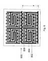
- FIG. 1One example of a UC-PBG structure 100 is shown in FIG. 1 .
- This UC-PBG structure 100contains a thin sheet of metal with a square lattice of Jerusalem crossed slots 112 .
- the UC-PBG structure 100may also be described as containing a unit cell 102 of a cloverleaf pattern with petals 104 , a center 106 , and a straight line segment 108 connecting adjacent centers 106 . Neighboring cloverleaf patterns 102 are separated by a gap 110 .
- Fries and Vahldieckdisclosed an example of a patch antenna employing the simple UC-PBG in place of a metal patch. They demonstrate a 50% area reduction (0.707 reduction in linear dimensions) with no added manufacturing complexity when both the patch and ground plane have the UC-PGB feature. However, leakage of RF power through the slotted ground plane is a potential EMI concern. In this case, the fundamental resonant frequency of the UC-PBG unit cell was much higher than the fundamental resonant frequency of the patch antenna.
- a DC inductive frequency selective surfacecan be used as a microstripline, resulting in a natural slow wave structure, which can be used to fabricate compact multi-band antennas.
- DCL FSSDC inductive frequency selective surface
- Some of these structureshave been investigated, for example the use of printed periodic transmission lines, or simply an array of circular holes, as the ground plane of a microstripline.
- a solid ground planemust be used to control leakage and radiation into the rear hemisphere and to define the printed trace of the microstripline to be periodic.
- An example of this caseis a one dimensional PBG cell proposed by Xue, Shum, and Chan. However, this is a 1-D patterned microstripline where only one layer of metal is used.
- DC FSS technologyis an economical way to create a printed slow wave structure usable for reduced size resonators in antenna and filter applications. Such resonators can be multi-band with engineered non-harmonic resonant frequencies.
- a number of factorsneed to be considered. First, slots in the ground planes of antennas are avoided as they tend to exacerbate the front-to-back ratio. Second, the simplest DCL FSS, the UC-PBG, reduces the physical size of a printed patch antenna where the patch is a UC-PBG structure.
- DCL FSSteaches derivatives and alternative designs to the published UC-PBG FSS pattern that resonate at much lower frequencies for a given period. This means that DCL FSS structures can have length scales much smaller than the free space wavelengths where they resonate.
- the application of DCL FSS technology to fabricate an extremely compact antennais shown, as is its theory of operation in simple to understand terms, which yields insight into the physics of the wave propagation. These antennas may yield multiband and non-harmonically related resonant frequencies.
- the DCL FSSis a dispersive surface defined in terms of its parallel LC equivalent circuit.
- Significant features of various printed circuit embodimentsinclude methods of enhancing the inductance and capacitance of the DCL FSS equivalent circuit to obtain a pole frequency as low as 300 MHz. Even designs without lumped surface mounted components resonate as low as L-band, which makes this material technology very attractive for wireless applications.
- One characteristic featureis that the effective sheet impedance model for the DCL FSS has a resonant pole whose free-space wavelength can be greater than 10 times the FSS period.
- a conductor-backed DCL FSScan be employed to create a form of high-impedance surface called a DC inductive artificial magnetic conductor (DCL AMC).
- DCL AMCDC inductive artificial magnetic conductor
- AMC resonant frequenciesare demonstrated as low as 2 GHz using simple, printed, low frequency enhanced DCL FSS structures.
- Lorentz polescan be introduced into the DCL FSS to create a multi-resonant DCL AMCs.
- One type of single-band elementis a bent-wire monopole on the DCL AMC.
- Another type of single-band elementis a multi-band shorted patch, similar to PIFA, except that the patch or PIFA lid is a DCL FSS. Multi-band designs, such as dual and triple band designs are possible.
- One of the antenna design factorsis the need to reduce the size of mobile terminal antennas.
- the antenna's largest dimensionis often restricted to be no more than ⁇ /10 at the low band, which is typically near 44 mm for 800 MHz in most mobile terminals.
- Another needis to provide usable radiation efficiency, typically greater than 25%.
- Additional design factors that must be considered in fabricating the DCL FSSinclude the need for multiple resonant frequencies that are almost always non-harmonically related, as well as the stability of the antenna resonant frequency in the presence of other objects. To restate the latter factor: the electrically small multi-band antenna should not be easily de-tuned by the presence of nearby objects. All of these factors must be addressed for internal antennas designed for modem mobile terminals.
- a first embodiment of an FSScomprises a first conductive layer having a periodic structure of individual first capacitive patches connected by an inductance greater than an inductance of a single straight line segment between the first capacitive patches.
- the inductancemay comprise a discrete inductor or may comprise a meanderline having a length substantially longer than the length of the single straight line segment between the first capacitive patches.
- the meanderlinemay have different characteristics: being at least twice as long as the length of the single straight line segment between the first capacitive patches, being coplanar with the first capacitive patches, being out of plane with the first capacitive patches, e.g. disposed on a secondary layer substantially parallel with and spaced from the conductive layer.
- the secondary layer and the conductive layermay be separated by a distance of about 5 mils to about 110 mils.
- the first capacitive patchesmay be rotationally symmetric and may comprise a spiral inductor and an interdigital capacitor.
- the first capacitive patchesmay be substantially spiral shaped.
- the FSSmay further comprise a second conductive layer having a second periodic structure of capacitive patches that are isolated from each other and have a series of fingers that overlap the spiral of a corresponding first capacitive patch.
- Each first capacitive patchmay have a substantially identical shape.
- the FSSmay further comprise a second conductive layer having a second periodic structure of capacitive patches, the capacitive patches isolated from each other and the first capacitive patches and overlapping a corresponding first capacitive patch of the first conductive layer.
- Each capacitive patchmay overlap each of a plurality of corresponding first capacitive patches of the first conductive layer.
- Each capacitive patchmay comprise a loop.
- a periodicity of each periodic structuremay be at most 250 mils.
- An LC circuit that models the FSSmay comprise a parallel combination of a first effective inductance and a second effective inductance, the second effective inductance in series with an effective capacitance, the first effective inductance being not less than about 5 times larger than the second effective inductance.
- the LC circuitmay comprise a parallel combination of an effective inductance and an effective capacitance.
- the inductancemay be at least 4 nH/square while the capacitance of the frequency selective surface may be at least 2 pF/square.
- DC inductive FSS structuresmay be employed as bandpass filters with center frequencies as low as 300 MHz.
- the effective LC circuitmay have a pass band with a center frequency of about 200 MHz to about 450 MHz and may have a pole at a frequency substantially lower than 10 GHz.
- the FSScomprises a first conductive layer having an inductive grid and a periodic structure of individual first capacitive patches coplanar with the inductive grid but isolated from both the inductive grid and each other.
- the inductive gridmay comprise a meanderline having a length substantially longer than a length of a single straight line segment between intersections of the inductive grid.
- the meanderlinemay be coplanar or out of plane.
- the FSSmay comprise a second conductive layer having a second periodic structure of second capacitive patches isolated from each other and the first capacitive patches and overlapping at least one section of each of a plurality of corresponding first capacitive patches of the first conductive layer.
- Each second capacitive patchmay also comprise a plurality of sections which overlaps a section of one of the corresponding first capacitive patches.
- Each first capacitive patchmay further comprise a loop and connections to connect neighboring sections of the first capacitive patch.
- Each first and second capacitive patchmay have a substantially identical shape.
- the FSSis modeled by an equivalent circuit having second Foster canonical form with a fundamental resonant frequency lower that of a second FSS consisting of a square lattice of Jerusalem crossed slots with a second period equal to the first period.
- the first periodmay be at most 1/10 of a free space wavelength at the resonance frequency of the FSS.
- the conductive layermay comprise a printed meanderline inductor.
- the meanderline inductormay comprise a printed spiral inductor and the conductive layer may further comprise a printed interdigital (comb-shaped) capacitor.
- the conductive layermay comprise a structure having a plurality of length scales within one unit cell.
- Such a conductive layermay comprise a fan blade structure with a grid that delineates sections of a first and second area.
- the sections of a first and second areamay each contain a plurality of smaller capacitive patches connected with the grid and having areas that depend on the area of the section.
- the adjacent capacitive patchesmay be connected by an inductor having an inductance greater than the inductance of the straight line segment connecting the adjacent capacitive patches.
- the inductormay comprise a discrete inductor or a meanderline having a length substantially longer than a length of the straight line segment connecting the adjacent capacitive patches.
- the meanderlinemay be coplanar with or out of plane with the first conductive layer of capacitive patches.
- the capacitive patchesmay comprise a single solid square, a cloverleaf, or a loop.
- the adjacent capacitive patchesmay be connected through the straight line segment.
- the first conductive layermay further comprise an inductive grid that surrounds the capacitive patches and the capacitive patches isolated from each other and the inductive grid.
- a second conductive layer of capacitive patchesmay be separated and isolated from the first conductive layer of capacitive patches and overlap a plurality of the capacitive patches of the first conductive layer.
- the FSScomprises a first conductive layer having a periodic structure of capacitive patches and a second layer separated from the first conductive layer.
- the second layeris coupled to the first conductive layer such that one of an effective inductance and capacitance of an effective LC circuit that models electromagnetic characteristics of the FSS is substantially affected by presence of the second layer.
- the period of the frequency selective surfacemay be at most 1/10 of a free space wavelength at the resonance frequency of the frequency selective surface.
- the first conductive layermay comprise a printed meanderline inductor.
- the meanderline inductormay comprise a printed spiral inductor and the first conductive layer may further comprise a printed interdigital (comb-shaped) capacitor.
- the second layermay comprise capacitive patches each of which overlaps a plurality of the spiral inductors.
- the capacitive patchesmay comprise a structure having a plurality of length scales. Such capacitive patches may comprise a fan blade structure with a grid that delineates sections of a first and second area. The sections of first and second area may each contain a plurality of smaller capacitive patches connected with the grid and having areas that depend on the area of the section. The second layer may comprise capacitive patches that overlap the smaller capacitive patches.
- Adjacent capacitive patchesmay be connected by an inductor having an inductance greater than the inductance of a straight line segment connecting the adjacent capacitive patches.
- the inductormay comprise a discrete inductor or a meanderline having a length substantially longer than a length of the straight line segment connecting the adjacent capacitive patches.
- the meanderlinemay be coplanar with the first conductive layer of capacitive patches, out of plane with the first conductive layer of capacitive patches and the second layer, or the second layer may comprise the meanderline.
- the capacitive patchesmay comprise a single solid square, a cloverleaf, or a loop.
- Adjacent capacitive patchesmay be connected through a straight line segment.
- the first conductive layermay further comprise an inductive grid that surrounds the capacitive patches and the capacitive patches isolated from each other and the inductive grid.
- the second layermay comprise capacitive patches isolated from each other and the capacitive patches of the first conductive layer, the capacitive patches of the second layer separated from and overlapping a plurality of capacitive patches of the first layer.
- the FSScomprises a single conducting layer having a periodic structure with a first characteristic length scale corresponding to an inductive grid and a second characteristic length scale corresponding to first capacitive patches, the first capacitive patches having at least two different sizes and each first capacitive patch being connected at a comer to a node of the inductive grid.
- the FSSmay comprise an additional layer of second capacitive patches overlying the first capacitive patches and providing a capacitance that reduces a resonant frequency of the FSS without increasing a period of the periodic structure.
- a method of reducing planar dimensions of a frequency selective surface having unit cells with an effective inductance-capacitance circuit of a first effective inductance in parallel with a series combination of an effective capacitance and a second effective parasitic inductance while retaining a frequency of electromagnetic waves propagating along the frequency selective surfacecomprises increasing the first effective inductance to substantially greater than an inductance of a straight line segment between the unit cells of the frequency selective surface and while not substantially increasing the second effective inductance.
- a method of reducing planar dimensions of a frequency selective surface having an effective inductance-capacitance circuit of a first effective inductance in parallel with an effective capacitance while retaining a frequency of electromagnetic waves propagating along the frequency selective surfacecomprises increasing the effective capacitance by overlapping capacitive patches of a periodic structure forming the frequency selective surface with capacitive patches offset from the frequency selective surface by a predetermined amount.
- a method of decreasing a lowest pole frequency of electromagnetic waves propagating along a frequency selective surface below 10 GHzcomprises connecting periodic first capacitive patches disposed on a conductive layer of the frequency selective surface through a meanderline disposed on a secondary layer.
- a method of decreasing a lowest pole frequency of electromagnetic waves propagating along a frequency selective surface below 10 GHzcomprises isolating periodic capacitive patches disposed on a first conductive layer of the frequency selective surface from other elements and periodic capacitive patches on a second conductive layer, isolating the patches on each layer from other patches on the same layer and from other patches on the other layer, and overlapping the patches on different layers.
- a method of decreasing a lowest pole frequency of electromagnetic waves propagating along a frequency selective surface below 10 GHzcomprises connecting periodic capacitive patches disposed on a first conductive layer of the frequency selective surface with each other, isolating periodic capacitive patches on a second conductive layer from other patches on the second conductive layer and the patches of the first conductive layer, and overlapping the patches on the first and second conductive layers.
- FIG. 1is a top view of a conventional UC-PBG FSS
- FIGS. 2 a-cillustrate equivalent circuits of a DCL FSS
- FIGS. 3 a and bare top views of different embodiments for DCL FSS
- FIGS. 4 a and bare a top view of another embodiment, used as a bandpass filter, and a plot of the transmission and return loss of this embodiment;
- FIG. 5illustrates a top view of another low frequency embodiment of a DCL FSS
- FIGS. 6 a and billustrates top and cross-sectional views of another embodiment of a DCL FSS
- FIGS. 7 a and billustrates top and bottom views of a multi-layer embodiment for a DCL FSS
- FIG. 8shows a top view of another embodiment of a DCL FSS employing a single conductive layer
- FIGS. 9 a and billustrate top views of upper and lower conductive layers of another embodiment of a DCL FSS
- FIGS. 10 a and billustrate top views of upper and lower conductive layers of another embodiment of a DCL FSS
- FIG. 11shows a top view of another embodiment of a DCL FSS
- FIG. 12shows a top view of another embodiment of a DCL FSS
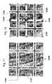
- FIGS. 13 a-cillustrate top views of upper and lower conductive layers of another embodiment of a DCL FSS as well as the combination of the upper and lower conductive layers of the embodiment;
- FIGS. 14 a-cillustrate top views of upper and lower conductive layers of another embodiment of a DCL FSS as well as the combination of the upper and lower conductive layers of the embodiment;
- FIG. 15illustrates a top view of another embodiment of a DCL FSS
- FIGS. 16 a-cillustrate top views of upper and lower layers of another embodiment of a DCL FSS as well as the combination of the upper and lower layers of the embodiment;
- FIG. 17illustrates a top view of another embodiment of a DCL FSS
- FIG. 18illustrates a top view of another embodiment of a DCL FSS
- FIG. 19illustrates a top view of another embodiment of a DCL FSS
- FIG. 20illustrates a top view of another embodiment of a DCL FSS
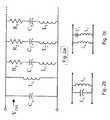
- FIGS. 21 a and billustrate a top view and equivalent circuit diagram of another embodiment of a DCL FSS
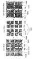
- FIGS. 22 a-eare perspective views of individual components of another embodiment of a DCL FSS, illustrated within a unit cell;
- FIGS. 23 a and billustrate an equivalent circuit diagram and dispersion diagram of phase constant vs. frequency of another embodiment
- FIGS. 24 a-dillustrate top view, cross-sectional, end, and perspective views of another embodiment
- FIGS. 25 a-care plots of characteristics of the embodiment of FIGS. 24 a-d;
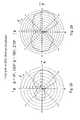
- FIGS. 26-29are gain plots of the embodiment of FIGS. 24 a-d.
- FIGS. 30 a-dillustrate top view, cross-sectional, end, and perspective views of another embodiment.
- the frequency selective surfaces (FSS) in the embodiments beloware electrically-thin, periodic, printed circuit boards.
- a FSSmay be formed from a multi-layer printed circuit board, not just a single thin layer of metal, or just a single layer of metal etched on a dielectric layer.
- the corresponding equivalent circuitis shown in FIG. 2 a.
- Each series RLC branchmanifests an intrinsic higher order resonance of the FSS.
- R nis expected to be very low, hence resonances are expected to be Lorentzian.
- a Lorentz resonanceis characterized by the effective sheet capacitance becoming infinite in magnitude, and changing it sign at the Lorentz resonant frequency. Every series RLC branch models a separate Lorentz pole for the admittance function.
- the circuit element C 0is the high frequency limit for shunt capacitance.
- L 0 and C 0are needed to accurately model the FSS, such as shown in the schematic of FIG. 2 b.
- there is a zero in the admittance function, or a pole in the impedance function, at ⁇1/ ⁇ square root over (L 0 C 0 ) ⁇ .
- the pole in the impedance functionis also called the fundamental resonance, or the fundamental pole frequency.
- FIG. 3 aA first embodiment of such a DCL FSS is shown in FIG. 3 a.
- the effective inductance L 0 of the conventional Jerusalem cross slotted FSS structureis increased with the addition of surface mounted chip inductors.
- the conductive layer 300thus contains unit cells 302 formed by a cloverleaf pattern with four petals (also called Cohn squares) 304 and a center 306 .
- the conductive layeralso contains straight line segments 308 forming an inductive grid by connecting adjacent centers 306 at substantially the middle of the edge of the center 306 .
- a gap 310separates adjacent capacitive patches 304 .
- Another way to describe thisis a simple square shape with notches cut into the center of the edges of the squares and straight line segments disposed in the notches.
- the effective sheet inductanceis formed by the grid of straight line segments 308 as well as the connections between the petals 304 and the center 306 of the cloverleaf 302 .
- Discrete inductors 312are placed in series with the straight line segments 308 to increase the inductance of these segments 308 .
- the DCL FSShas an equivalent circuit denoted by FIG. 2 c.
- a capacitive patchis shown in the FIG. 3 a, for example, as a simple square, other shapes are possible to achieve the desired capacitance. Shapes can include, but are not limited to, quadrilateral, rectangular, hexagonal, circular, ovate, or parallelepiped shapes, a loop, interdigital fingers, and inductive spirals, or any combination thereof.
- the addition of the discrete inductorsmay not be desirable to decrease the resonant frequency and establish the desired low frequency.
- the resonant frequencymay also be decreased by increasing the effective capacitance.
- the effective capacitanceis essentially formed by the edge-to-edge capacitive coupling between the adjacent petals 304 of the unit cell 302 .
- the length of the edges of the capacitive patches 302may be increased.
- the edges of the capacitive patches 302are increased, the area of the capacitive patch 302 is increased and overall the size of the layer increases.
- an out of plane conductive layerthat is, a second conductive layer of capacitive patches that overlaps the patches on the first conductive layer such that a significant parallel plate capacitance is achieved that links the adjacent capacitive patches 304 .
- the second layer of patchesincreases C 0 , but does not block the magnetic flux that passes through the slots next to the inductive grid.
- FIG. 3 bin which the second layer of patches 318 contains capacitive patches 320 that have substantially the same dimensions and period as the patches 302 of the first layer 300 .
- Each capacitive patch 320 in the second conductive layer 318overlaps four petals 304 , each petal 304 in an adjacent unit cell 302 on the first conductive layer 300 .
- the patches 320 of the second layer 318are not required to have any particular shape, the important feature being the overlap area of the underlying first layer of patches 302 by the overlying area of the second layer of patches 320 .
- the overlapping second layer of patchesmay be formed from the same printed circuit structure as the first layer of patches, for example a cloverleaf structure whose petals overlap petals of the underlying first layer of patches and whose center and straight line segments are disposed essentially in between the cloverleaf patches of the underlying first layer of patches.
- An FSS dielectric spacer layer(not shown) having a relatively low permittivity separates the underlying first layer of patches 302 and the overlying second layer of patches 320 such that a parallel plate capacitance is formed between the first and second sets of patches 302 and 320 . This capacitive coupling is enhanced by the dielectric constant of the printed circuit material.
- the chip inductorshould have a self-resonant frequency much higher than the intended resonant frequency of the DCL FSS to be an effective inductor.
- FIG. 4 aAn embodiment of such a DCL FSS is shown in FIG. 4 a.
- the FSS 400contains an upper layer of capacitive patches 402 that are simple solid squares of conductive material, such as metal. These capacitive patches 402 are connected to adjacent squares by surface mounted chip inductors 404 disposed substantially in the center of each edge. The capacitive patches 402 are separated by a gap 406 .
- An underlying second layer of square capacitive patches(not shown) are disposed below the overlying first layer of capacitive patches 402 in the same manner as the structure shown in FIG. 3 b.
- the first and second layers of capacitive patchesare likewise separated by a FSS dielectric 408 .
- the center frequency, or resonant frequencymay be selected to be about 300 MHz. Plots of normal incidence plane wave transmission and return loss of such a realized FSS are shown in FIG. 4 b.
- the FSShas a period that is substantially smaller than the free space wavelength at resonance (here ⁇ /145).
- the particular design from which the plots originateused 82 nH Coilcraft inductors of the 0805HT series.
- the FSSused 260 mil overlapping patches on a period of 270 mils, i.e.
- the gap between the squareswas 10 mils.
- Two dielectric layers of 8 mil Rogers R04003were used, one to separate layers of patches and the other disposed under the underlying layer of patches. Measurements were made using a plane wave transmission and reflection test over a frequency range sufficient to identify the fundamental resonant frequency.
- a meanderlinealso called meanderline inductor
- the meanderlineis essentially merely a non-straight line conductive path between adjacent patches.
- embodiments with a meanderline inductormay be a single, planar structure that rely on edge-to-edge capacitance, or it may rely on overlapping capacitive patches to lower the fundamental resonant frequency.
- An embodiment of the latter type of FSSis shown in FIG. 5 .
- solid conductive patches 520overlap the petals 504 of the underlying cloverleaf unit cell pattern 502 and adjacent centers 506 of the cloverleaf unit cell patterns 502 are connected by coplanar meanderlines 508 .
- the solid conductive patches 520 and cloverleaf patterns 502are separated by a FSS dielectric (not shown).
- DCL FSS structureBefore illustrating further examples of such a DCL FSS structure, one method of designing these structures will be discussed.
- the equivalent circuit of the conventional UC-PBGwas inadequate to model the FSS embodiments, including any derivatives with coplanar meanderline inductors.
- the prior artdoes not teach that an inductance is needed in series with the shunt capacitance C 0 to account for the presence of the notches in each patch, as shown in FIG. 2 c, which shows a more complete equivalent circuit topology including the notch inductance modeled as L 1 .
- the notch inductancein fact, can be 10% or more of the grid inductance L 0 .
- FIGS. 6 a and 6 bThe top and cross-sectional views of another embodiment of a DCL FSS are shown in FIGS. 6 a and 6 b.
- the upper layer of patches (solid squares) 620are shown as dashed lines and the dielectric layer 610 between the upper conductive layer of patches 620 and the lower conductive layer of patches 602 (cloverleaf with meanderline) are shown as a solid layer.
- the patches 602 of the lower conductive layerhave petals 604 and a center 606 .
- the centers 606 of adjacent patches 602are connected through the meanderline 608 .
- the upper and lower conductive layers of patches 602 and 620are separated by a FSS dielectric layer 610 and a dielectric spacer 612 is disposed beneath the lower conductive layer of patches 602 .
- each of the upper and lower array of patchesis 250 mils, gaps between these patches (without the meanderline between the patches) 614 as well as line widths of the meanderline are each 10 mils.
- FIG. 6 bshows a top layer of capacitive patches 620 printed on a thin (2 mil) layer of polyimide ( ⁇ r ⁇ 3.5) as the FSS dielectric 610 .
- a thicker (62 mil) lower dielectic spacer of FR 4 ( ⁇ r ⁇ 4.5)is disposed below the second layer of capacitive patches 602 .
- a ground planeis separated from the FSS.
- capacitive patches on at least one conductive layer of the FSSare connected to the ground plane through support posts (vias).
- the separation between the FSS and the ground planemay be realized by air or the lower dielectric spacer 612 .
- any DCL FSS design using a coplanar meanderlinecan offer at best only 50% of the ⁇ 90° reflection phase bandwidth achievable from a Sievenpiper type high-impedance surface.
- One way to avoid thisis to move the inductive grid that connects the capacitive patches of a particular conductive layer out of plane relative to that conductive layer as well as out of plane of any conductive layer within the DCL FSS that contains capacitive patches. This eliminates the notch inductance from the equivalent circuit model and increases the reflection phase bandwidth.
- FIGS. 7 a and 7 bOne embodiment for a low-frequency enhanced DCL FSS employing an out-of-plane inductive grid is shown in FIGS. 7 a and 7 b. Given a period of 250 mils, this embodiment can have a fundamental resonance at 600 MHz, for example.
- This FSS 700contains square capacitive patches 702 printed on one side of a 2 mil FSS dielectric (polyimide) 704 .
- a lower layer of capacitive patches (buried layer) 706is disposed on the opposing side of the FSS dielectric 704 .
- the buried layer of patches 706is attached to a 20 mil layer of FR 4 (dielectric spacer 712 ).
- the inductive grid 708 of 10 mil wide meanderlineis disposed on a surface opposing the buried layer of patches 706 .
- the meanderline 708has a period of 250 mil period, the same period as the layers of capacitive patches 702 and 706 .
- a plated through hole 710connects the inductive grid 708 to the center of one of the buried patches 706 .
- the equivalent circuit of such a structureis shown in FIG. 2 b.
- the LC valuesare 11 nH/square and 2.4 pF/square, yielding a fundamental resonance near 1 GHz.
- the period of the various conductive layersmay be as small as ⁇ /48 at resonance. No surface mounted components are needed in this embodiment, only a hybrid flex-rigid board with three metal layers and two dielectric layers.
- FIG. 8One embodiment of such an FSS 800 is shown in FIG. 8 .
- the unit cellincludes a meanderline inductor 804 as well as fingers 806 that form interdigitated capacitors.
- the embodiment shownis a single layer structure with no overlapping patches (although they may be added as above).
- the meandering patternincreases the inductance, while the fingers 806 , which extend from the meanderline, form interdigitated capacitors that increase the capacitance.
- FIGS. 9 a and 9 bshow the layers of another embodiment employing the above concept.
- the capacitive patches 902 , and the spiral inductor 904are printed on opposite sides of an FSS dielectric (not shown), such as a conventional printed circuit board.
- FSS dielectricsuch as a conventional printed circuit board.
- the upper layer square patches 902are separated from the lower layer spirals 904 by the FSS dielectric.
- the upper layer square patches 902overlap a section of adjacent spirals 904 such that the capacitance and inductance of the FSS 900 are modeled as in FIG. 2 b.
- the patches 1002 of the upper layerdo not have to be solid squares.
- the inductance of the patches 1002may be increased while the parallel plate capacitance formed with the spirals 1004 remains substantially the same.
- the parallel plate capacitancewill remain substantially the same so long as the overlap between the material that forms the different patterns remains the same.
- DCL FSS structuresare described as being disposed on a rigid or flex-rigid printed circuit structures, it is possible to fabricate DCL FSS structures from flexible substrates alone.
- FIGS. 11-14Some of the embodiments are shown in FIGS. 11-14 .
- the inductive grid of the DC inductive FSS structuresis not directly connected to any of the metal islands which constitute the capacitive patches of the FSS.
- the capacitive patchesare fully isolated, i.e. isolated from the inductive grid and from other capacitive patches on the same plane.
- a variety of LC patternscan be integrated on the first layer, or added as a second layer, to supply Lorentz poles for the transverse permittivity.
- the DC isolated gridallows a control voltage or a control current to support integrated electronics. Prime power can be supplied via this grid.
- the inductive grid 1104 , 1204may be a set of straight lines while the capacitive patches 1102 , 1202 disposed between intersections of the inductive grid 1104 , 1204 may be solid conductive squares 1102 or cloverleaf patterns 1202 (each cloverleaf 1202 having petals 1206 and a center 1208 unconnected with adjacent cloverleaf centers).
- the effective circuit diagramsare illustrated in FIG. 2 b.
- FIGS. 13 a-c and 14 a-cillustrate the individual lower conductive layer 1302 , 1402 and upper conductive layer 1304 , 1404 of an FSS 1300 , 1400 as well as the overall combination 1306 , 1406 of the lower conductive layer 1302 , 1402 and upper conductive layer 1304 , 1404 .
- the overlapping patches of the upper layer in these figuresoverlap a plurality of patches of the lower conductive layer with an FSS dielectric (not shown) disposed between the lower conductive layer 1302 , 1402 and upper conductive layer 1304 , 1404 .
- FIGS. 13 a-cillustrate an embodiment in which the petals 1308 of the cloverleaf of the upper layer 1304 overlap petals 1314 of the cloverleaves of the lower layer 1302 to form the parallel plate capacitance of FIG. 2 c. Only the center 1316 of the cloverleaf of the upper layer 1304 overlaps the inductive grid 1312 of the lower layer 1302 . The center 1310 of the cloverleaf of the lower layer 1302 is not overlapped.
- FIGS. 14 a-cillustrate an embodiment in which the capacitive patches 1414 of the lower layer 1402 and the capacitive patches 1416 of the upper layer 1404 are non-symmetric. Both the capacitive patches 1414 of the lower layer 1402 and the capacitive patches 1416 of the upper layer 1404 have sub-patches 1420 , 1410 of different sizes within a given unit cell. The sub-patches 1420 of the lower layer 1402 substantially match the sizes of the sub-patches 1410 of the upper layer 1404 .
- the sub-patches 1420 of the lower layer 1402are connected to each other through meanderlines 1418 of different lengths, while the sub-patches 1410 of the upper layer 1404 are connected to each other through straight lines segments 1412 of the same length.
- the loops formed by the capacitive patches 1414 of the lower layer 1402 and the capacitive patches 1416 of the upper layer 1404increase the self-inductance of the patches.
- FIGS. 15 and 16Examples of such structures are shown in FIGS. 15 and 16 . As can be seen in the simple fan blade structure of the FSS 1500 FIG. 15 , a unit cell contains patterns formed using essentially the same pattern with two different sizes.
- the unit cellis defined using coordinate axes, x-y or u-v, tilted at a particular angle from the x-y axis.
- the embodiment shown in FIG. 15features an inductive grid of fan blades that are connected, not a capacitive grid of isolated fan blades.
- the fan bladesare rotationally symmetric with four fold discrete symmetry, and the inductive grid 1502 that forms the fan blades delineate squares of a first area 1504 and squares of a second area 1506 .
- FIG. 16illustrates a DCL FSS 1600 with a fan blade inductive grid 1602 similar to that shown in FIG. 15 .
- the delineated squares of FIG. 15each contain a plurality of smaller solid capacitive patches 1608 , 1610 with areas that depend on the area of the delineated square.
- each of the four capacitive patches 1608 , 1610are connected to the conductor that forms the inductive grid 1616 via a straight line segment 1612 .
- the straight line segment 1612is connected at the corners of the capacitive patches 1608 , 1610 , runs diagonally to the grid 1616 , and is connected to the grid 1616 at T intersections 1614 of the grid 1616 (the corners of the delineated squares).
- an additional upper conductive layer 1604 as shown in FIG. 16 bmay be added to reduce the fundamental resonant frequency of the single layer structure.
- the upper conductive layer 1604contains solid patches 1618 , 1620 of different sizes. The different sizes and positions of these solid patches 1618 , 1620 are aligned with the delineated squares such that the capacitive patches 1608 , 1610 of the lower conductive layer 1602 are substantially overlapped without overlapping the grid 1616 .
- the solid patches 1618 , 1620are disposed such that they overlap both the areas of the capacitive patches 1608 , 1610 of the lower conductive layer 1602 and the gaps between the capacitive patches 1608 , 1610 of the lower conductive layer 1602 .
- the size and shape of either patchis not critical.
- the solid patches 1618 , 1620may be further increased in number, decreased in size and aligned such that they overlap the capacitive patches 1608 , 1610 of the lower conductive layer 1602 but do not overlap the gaps between the capacitive patches 1608 , 1610 of the fan blade 1602 .
- FIGS. 17-23illustrate yet another set of embodiments of DCL FSS structures that are multi-resonant.
- the embodiment shown in FIG. 17may be used whereby, two closely spaced conductive layers are separated by a dielectric layer.
- the simple square capacitive patches of FIG. 3 bmay be transformed into loops.
- the loop comersform parallel-plate capacitors with the patches on the inductive grid layer while the notches form an inductance between the patches of the upper conductive layer.
- one side of the FSSmay be an array of Cohn squares, while the other side of the FSS is a crossed dipole FSS in which the ends of the dipoles are connected by chip inductors or very thin lines.
- the resultis a capacitive FSS layer, C c , in parallel with an inductive FSS grid, L 1 , that has a capacitor, C t , in tank with part of its inductance L 2 .
- the relative sizes of the straight and looping sections of the inductive grid (and/or the value of the chip inductors)permit control of the relative sizes of the two inductors.
- the capacitorscan be given different relative sizes by controlling the edge-to-edge gap of the Cohn squares, the length of the inductive FSS grid's straight sections, or by adding a third capacitive FSS layer, staggered behind the Cohn squares layer to increase its capacitance without affecting the inductive grid.
- FIGS. 17 and 18show an FSS 1700 , 1800 in which one layer of the FSS 1700 , 1800 contains an array of the cloverleaf capacitive patches 1702 , 1802 while another layer contains a loop 1704 , 1804 .
- capacitive patches 1704 , 1804 of the upper layerhave been modified from a simple square to a square with an internal cutout that substantially matches the gaps between the cloverleaf capacitive patches in the underlying layer 1702 , 1802 .
- the only differences between the FSS in FIGS. 17 and 18is that in FIG.
- the Cohn squares 1706 that form the petals of the capacitive patches in the underlying layer 1702 , 1802 as well as the squares 1720 of the overlap layer 1720have the same area.
- the areas of three out of the four petals 1806 of the underlying cloverleaf patches 1802 , as well as the corresponding squares 1820 of the overlap loopare unequal (this alters the length and the width of the straight line segments 1708 , 1808 connecting the corners of the squares 1720 , 1820 ).
- the changes in the amount of overlap as well as the connections been the individual squaresalters both the capacitance and the inductance of the FSS.
- the sections of the patches on the overlying layer that form the parallel plate capacitance with the underlying layersubstantially match the size and position of the petals on the underlying cloverleaf.
- FIGS. 19-21illustrate other embodiments in which the inductance in series with the upper conductive layer of capacitive patches is increased.
- the main difference between the FSS 1800 of FIGS. 18 and the FSS 1900 , 2000 of FIGS. 19 and 20is that the squares 1904 , 2004 that form the loop 1902 , 2002 in the upper layer of capacitive patches are connected by a longer straight line segment 1906 ( FIG. 19 ) or a meanderline 2006 ( FIG. 20 ) that has a plurality of segments to increase the length of the connection between the squares 2004 .
- FIG. 21 aillustrates a multi-resonant DCL FSS 2100 whereby an upper conductive layer has a unit cell 2102 with a loop 2104 that has squares 2108 connected by a straight line segment 2106 .
- the straight line segments 2106connects the squares 2108 at the center of the sides of the squares 2108 , notches are formed in the squares 2108 , and the length, but not the width of the straight line segments 2106 of at least some of the straight line segments 2106 are different.
- FIG. 21 bshows the approximate equivalent circuit of the entire structure of FIG. 21 , including the upper and lower FSS layers as seen by a y-polarized normally-incident electric field.
- Z eq[ j ⁇ ⁇ ⁇ L 1 ⁇ ⁇ ⁇ ⁇ 1 j ⁇ ⁇ ( C g1 + C g2 ) ] ⁇ ⁇ ⁇ ⁇ [ Z 1 + Z 4 + ( j ⁇ ⁇ ⁇ L 2 + Z 2 + Z 5 ) ⁇ ⁇ ⁇ ⁇ ( j ⁇ ⁇ ⁇ L 3 + Z 3 + Z 6 ) ] ⁇ ⁇
- the effective sheet impedance, Z eqhas poles at four frequencies which may be user defined and non-harmonically related.
- lumped series inductors in the square grid and/or overlay capacitors of secondary layersmay be added to dramatically reduce the fundamental resonant frequency of the FSS.
- multi-resonant DCL FSS structurescan be employed in multi-band AMCs if conductor backed (i.e. a ground plane is separated from the DCL FSS), or used in multi-band patch antennas if they are employed as the patch or ground plane.
- a multi-band DCL AMCis a type of high impedance surface that can be fabricated by employing the above multi-resonant DCL FSS structures and placing these FSS structures parallel and electrically close to a simple metal ground plane (a continuous sheet of conductor). The high impedance surface is the FSS side. Unlike the conventional Sievenpiper AMC, the DCL AMC does not have vertical conductors connecting capacitive patches of the FSS to the ground plane.
- any of the low frequency enhanced DCL FSS structures described abovemay be conductor-backed, with a dielectric substrate or air spacer in between, to realize a low frequency enhanced DCL AMC.
- the more complex members of this DCL AMC familyhave multiple poles in the analytic function which defines the FSS transverse permittivity, ⁇ t .
- FIG. 22 a-eOne embodiment of a DCL AMC is shown in FIG. 22 a-e. It exhibits a TE mode cutoff for surface waves, but not a TM mode cutoff, in the frequency range near the high impedance band (the ⁇ 90° bandwidth).
- This embodimentis essentially the same as the FSS shown in FIGS. 7 a and 7 b with the addition of a ground plane.
- the ground plane 2202is separated from the lower layer of capacitive patches 2206 by an FR4 dielectric substrate 2212 .
- the inductive grid 2204is disposed within the dielectric substrate 2212 .
- the center of each unit cell of the inductive grid 2204is connected with the center of the capacitive patches on the lower layer of capacitive patches 2206 using a 0.25 mm via 2214 .
- the lower layer of capacitive patches 2206is separated from the upper layer of capacitive patches 2208 by an FSS dielectric 2210 comprised of 2 mils of polyimide.
- the period of the upper and lower layers of capacitive patches 2306 and 2308is the same, 6.25 mm.
- the capacitive patches 2306 and 2308are 5.25 mm on each edge of the square.
- the reflection phase bandwidth of this DCL AMC 2200is measured to be nominally from 1900 MHz to 2060 MHz with resonance near 1990 MHz, a TE mode cutoff near 2.0 GHz, and no TM mode cutoff near 2.0 GHz (i.e. no TM mode cutoff near its high impedance bandwidth).
- the valuesare merely exemplary and may be altered as desired, depending on many factors such as the shape and area of the patches and inductive grid or thicknesses of the FSS dielectric and dielectric substrate for example.
- PIFAplanar inverted F antenna
- PIFA structureshave been discussed at length, for example in provisional application No. 60/354,003 filed Jan. 23, 2002 and entitled, “DC INDUCTIVE SHORTED PATCH ANTENNA” herein incorporated by reference.
- a PIFAexhibits one resonant frequency when the lid of the PIFA is simple conductive layer (metal patch). However, if a DCL FSS is substituted for the lid, then a multi-band resonator may be realized.
- the PIFA cross-sectionmay be viewed as a transmission line supporting a fast wave and a slow wave.
- the open and short circuit boundary conditions on the ends of the PIFAforce both waves to be standing waves.
- the equivalent circuit diagram of the transmission line structureis shown in FIG. 23 a while a phase constant vs. frequency plot is shown in FIG. 23 b.
- the phase constant ⁇can be calculated from an equivalent circuit model which models the per unit length properties of the transmission line, as shown in FIG. 23 a.
- L 1 and C 1model the magnetic and electric field energy stored in the DCL FSS while L 2 and C 2 model the energy stored in the external magnetic and electric fields which surround the microstripline.
- a stopbandexists between the two frequencies, ⁇ p and ⁇ z .
- the PIFA resonant frequenciesare given by the intersection of the phase constant curves with the ⁇ 0 line.
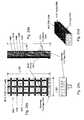
- FIGS. 24 a-dshow the top, cross-sectional, end, and perspective views, respectively of a PIFA 2400 .
- the capacitive patches 2402(here solid squares) are shown in the top view of the PIFA 2400 in FIG. 24 a.
- the capacitive patches 2402are fabricated on a thin FSS dielectric 2404 (printed circuit board) and an inductive grid 2406 is formed on the opposing surface of the printed circuit board 2404 .
- the combination of the capacitive patches 2402 , FSS dielectric 2404 , and an inductive grid 2406form the DCL FSS 2420 .
- a thick dielectric substrate 2408separates the inductive grid 2406 and the ground plane 2410 .
- the dielectric substrate 2408may be formed from a low permittivity material such as foam.
- the DCL FSS 2420may be attached to the foam substrate 2408 either permanently or temporarily, for instance by using repositionable spray adhesive.
- a conductive material 2416such as the copper foil used here, is used to ground the end of the array of capacitive patches 2402 to the ground plane 2410 .
- the metal 2416 placed on the end of the array 2402is called the PIFA short or shorting wall. It is not necessary that the ground plane 2410 be formed from the same material as the PIFA short 2416 as shown in the figures.
- the ground plane 2410is formed from a flexible material as shown, such flexibility may not be essential—the ground plane may be formed from a thicker, more rigid layer of conductive material or may be buttressed by a separate rigid layer. The detriment to this is that such a layer will add thickness and weight to the overall PIFA structure.
- the DCL FSS 2420is fabricated such that the capacitive patches 2402 terminate in a set of half patches 2418 , i.e. the end of the DCL FSS 2420 aligns with the center of one of the patches 2418 .
- the PIFA short 2416is attached to the end of the layer of capacitive patches 2402 such that it contacts the half patches 2418 and does not contact any vertical conductors (vias) 2412 . Altering the fabrication of the DCL FSS 2420 such that the edges of the capacitive patches 2402 does not align with the center of one of the patches will change the electrical characteristics of the PIFA 2400 .
- a feed probe 2412is a via that feeds signals to the DCL FSS 2420 through the dielectric substrate 2408 .
- the feed probe 2412is connected with one of a plurality of plated through holes 2422 disposed between the capacitive patches 2402 .
- a forest of viasmay exist depending on the fabrication method (only one of which is the feed probe).
- the feed probe 2412is feeding signals through a connector 2414 , here a SMA connector, disposed on the ground plane 2410 .
- the outer surface of the connector 2414may be connected to, and thus share a common ground with, the ground plane 2410 .
- the center conductor (not shown) of the SMA connector 2414is extended using 24 AWG wire to form the feed probe 2412 .
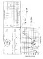
- FIGS. 25 a-care plots of experimental results for the PIFA of FIGS. 24 a-d.
- FIG. 25 ashows the return loss of the PIFA 2400 as a function of frequency.
- FIGS. 25 b and cshow the efficiency and gain of the PIFA 2400 as a function of frequency.
- DCL FSS structuresthat exhibit not one, but two frequencies where the effective sheet impedance becomes infinite, or exhibits a parallel resonance.
- Such embodimentscan be realized by cascading unit cells of two different simple DCL FSS designs, such as that shown in the fan blade structures of FIGS. 15 and 16 .
- a triple-band PIFAfor example, which resonates at three different frequencies, may be fabricated from these DCL FSS structures when the DCL FSS is used as the lid of the PIFA.
- PIFAsare not the only radiating structures that can use DCL FSS structures.
- DCL AMCs that use DCL FSS structurescan be used to make an electrically thin antenna.
- An example of such an antennais an antenna element, for example a bent-wire monopole, that is disposed electrically and physically close to the DCL AMC.
- FIGS. 30 a-dshow the top, cross-sectional, end, and perspective views, respectively of the antenna element 3000 .
- the capacitive patches 3002 of the antenna 3000are fabricated on a thin FSS dielectric 3004 and an inductive grid 3006 is formed on the opposing surface of the FSS dielectric 3004 .
- a thick FR4 dielectric substrate 3008separates the inductive grid 3006 and the ground plane 3010 .
- the combination of the capacitive patches 3002 , FSS dielectric 3004 , an inductive grid 3006 , and ground plane 3010forms a DCL AMC 3020 .
- the DCL AMC 3020is fabricated such that the capacitive patches 3002 terminate in a set of half patches 3018 , i.e. the end of the DCL AMC 3020 aligns with the center of one of the patches 3018 .
- the antenna 3000 of this embodimentdoes not require a short on the end of the capacitive patches. Rather, the antenna 3000 can use an RF short formed by a pair of grounded vias 3016 that connects the ground plane 3010 to the inductive grid 3006 . Such a connection is important to achieve a reasonable impedance match.
- the RF shortis fabricated by drilling two additional small holes through the DCL AMC 3020 for the grounded vias 3016 and soldering the grounded vias 3016 to plated through holes 3026 in the inductive grid, the ground plane 3010 and between the capacitive patches 3002 .
- the grounded vias 3016 that form the RF shortare disposed at comers of the capacitive patches 3002 , horizontally adjacent to the feed probe 3012 and one half of a period from the feed probe 3012 .
- the feed probe 3012is an additional hole drilled between the grounded vias 3016 .
- a bent-wire monopole 3022 or other suitable antenna structureis disposed on an antenna dielectric 3024 .
- the bent-wire monopole 3022 and antenna dielectric 3024are disposed close to the capacitive patches 3002 for efficient radiation of a signal fed to the bent-wire monopole 3022 .
- the bent-wire monopole 3022is 1.375′′ long and 0.050′′ wide and is disposed on a 0.031′′ FR4 dielectric.
- the bent-wire monopole 3022is excited through a feed probe 3012 that extends through the dielectric substrate 3008 and contacts only the center conductor of the coaxial feedline.
- the feed probe 3012excites the bent-wire monopole 3022 from a SMA connector 3014 disposed on the ground plane 3010 .
- the outer surface of the connector 3014may be connected to the ground plane 3010 .
- the center conductor (not shown) of the SMA connector 3014is extended using 24 AWG wire to form the feed probe 3012 .
- This antenna 3000is characterized by a relatively small size ( ⁇ 0.19 ⁇ 0.33 ⁇ 0.023 ⁇ ) with a very good front to back ratio of about 8 dB.
- the inputis extremely well matched to 50 ohms without any external matching circuit.
- the ⁇ 6 dB return loss bandwidthis about 9%.
- this antennauses a multi-layer low frequency enhanced DCL FSS and AMC, a simpler one-metal-layer FSS such as the UC-PBG may be used, with the caveat that the resonant frequency is expected to be higher than that of the multi-layer structure.
- any of the DCL FSS structures described hereincan be used, for example, embodiments containing the additional layer of capacitive patches.
- grounding viasmay be altered while maintaining acceptable response.
- four grounding viasmay be formed through the AMC. While the feed is again disposed between centers of the capacitive patches and the vias that form the shorting wall are again disposed at corners of the capacitive patches one half of a period from the feed in the horizontal direction, the vias are now offset by one period vertically towards the edge of the layer that contains the half capacitive patches.
- a PIFA similar to that shown in FIGS. 24 a-dis used.
- the vias that form the RF shortare replaced by the shorting wall of the PIFA, as in FIG. 24 c.
- Any plated through holes fabricated with the PCBmay remain uncontacted however.
- the above three configurations of the DCL AMC antennaswere fabricated and designed to resonated at about 2.0 GHz. Each configuration exhibited a return loss null at or slightly above the AMC resonant frequency.
- the antenna sizeswere all 1.0′′ ⁇ 1.75′′ ⁇ 0.125′′ ( ⁇ 0.191 ⁇ 0.331 ⁇ 0.0231 ⁇ ).
- the antenna patternhad a main beam at broadside, normal to the AMC surface.
- the best impedance matchwas given by the AMC antenna that used a conductive shorting wall at the end of the AMC structure. .
- the ⁇ 10 dB return loss bandwidthwas 115 MHz or 5.2%, the ⁇ 6 dB return loss bandwidth was about 200 MHz or 9.1%.
- the PIFA antennaalso had a front to back ratio of ⁇ 8 dB, peak and average gains of ⁇ 1.7 dBil and ⁇ 3 dBil, and a realized antenna efficiency peaks slightly above 50%.
- DCL FSS and related structures having a fundamental pole frequency f pin the analytic function modeling the equivalent sheet impedance, may be designed to be much less than one tenth of c/P where c is the speed of light and P is the FSS period. Equivalently, the period of the FSS is less than ⁇ /10 of the free space wavelength at the fundamental pole frequency.
- Some DCL FSS embodimentsmay exhibit multiple engineered pole frequencies in the equivalent sheet impedance of the FSS.
- the DCL FSSinclude an isolated grid DCL FSS, which contains an inductive grid that is coplanar with capacitive patches but DC isolated from the patches.
- the inductive gridmay be used to distribute prime power or to distribute control signals to integrated electronics.
- the DCL FSSalso includes a dual scale, multi-resonant UC-PBG FSS that contains a single metal layer having two characteristic length scales involving one inductive grid and two sizes of conductive patches. Each patch is connected at a one of its corners to a node of the conductive grid. Additional layers of conductive patches can be added as overlay capacitors to reduce the resonant frequencies without increasing the period.
- a low frequency DCL AMCwhich is a low frequency high-impedance surface, contains the above low frequency enhanced DCL FSS separated from a ground plane by a fixed distance.
- the DCL AMCmay have multiple bands.
- Such a multi-band DCL AMCincludes a DCL FSS that contains at least one Lorentz pole and is separated from a ground plane by a fixed distance.
- a DCL AMC antennacontains a DCL AMC and a printed strip or wire located parallel to and above the DCL AMC surface.
- the printed stripis fed via a vertical probe from a coaxial aperture in the ground plane.
- the ground planemay be extended up along one edge of the DCL AMC to make conductive contact with some or all of the metal patches or grid.
- Such a DCL AMC antennamay be useful in many mobile wireless applications, especially wherever it is desirable to have a relatively thin antenna, wherever it is desirable to have a front-to-back ratio of 8 dB or greater (especially important for body-worn applications), and wherever it is desirable to minimize the number of plated through holes in an AMC antenna design.
- the DCL FSS PIFAis a multi-band printed antenna comprised of a periodic transmission line shorted at one end.
- the DCL FSS PIFAhas a DCL FSS located above a ground plane with a short circuit at one end and essentially an open circuit at the other end.
- a feed probeis located between the two ends.
- the multi-band printed antennamay be modeled by a periodic transmission line in which the periodic unit cell of the transmission line has a particular equivalent circuit.
- the DCL FSS PIFAmay be useful in many mobile wireless applications, especially where it is desirable to resonate at two or more non-harmonically related frequencies, where it is desirable that the resonant frequencies are insensitive to changing environmental factors such as proximity to a human body and where the volume for antenna integration is extremely limited, approximately ⁇ /10 at most for the largest dimension, where ⁇ is the free-space wavelength at the lowest resonant frequency.
Landscapes
- Waveguide Connection Structure (AREA)
Abstract
Description
This application is a non-provisional application claiming priority to provisional application Ser. No. 60/310,655, filed Aug. 6, 2001.
The demand for reduced size consumer electronics has produced a corresponding demand for reduced size electronic components used in these electronics. In portable electronics such as cellular telephones, one of the necessary components is an antenna. The most common type of antenna in cellular telephones are whip antennas because they are relatively cheap and simple to fabricate. However, the gain-bandwidth product of a whip antenna is relatively poor and the size is large.
Uniplanar compact photonic bandgap (UC-PBG) structures have been demonstrated in an attempt to reduce the size of antenna. One example of a UC-PBG structure 100 is shown in FIG.1. This UC-PBG structure 100 contains a thin sheet of metal with a square lattice of Jerusalem crossedslots 112. The UC-PBG structure 100 may also be described as containing aunit cell 102 of a cloverleaf pattern withpetals 104, acenter 106, and astraight line segment 108 connectingadjacent centers 106.Neighboring cloverleaf patterns 102 are separated by agap 110.
In another example of a UC-PBG, K. P. Ma et al. showed that if one places a PEC surface parallel to and electrically close to the UC-PBG structure, then the UC-PBG surface exhibits properties of a high-impedance surface, where it has a zero degree reflection phase for plane waves at normal incidence. Later, Richard Remski at Ansoft Corp. predicted that a conductor-backed UC-PBG also exhibited a full electromagnetic bandgap for surface waves. This was done using finite element (FEM) software to perform an eigenmode analysis on the open structure. However, only one publication addresses the question of a surface wave bandgap for the conductor-backed UC-PBG. No experimental data has yet been published.
While the UC-PBGs above were a step in the right direction, ample motivation still exists to develop antenna technology and apply it to practical filter and antenna applications at UHF and L-band frequencies (300 MHz to 2 GHz) for commercial wireless bands. Previous work on UC-PBGs, for example, demonstrated a fundamental parallel LC resonance near 10 GHz using a period of 0.12 inches, or λ/10 where λ is a free space wavelength at the fundamental resonance. However, for most practical applications the period must be reduced to be much less than λ/10, typically between λ/50 and λ/25. Accordingly, reduction of the unit cell dimensions is necessary.
Fries and Vahldieck disclosed an example of a patch antenna employing the simple UC-PBG in place of a metal patch. They demonstrate a 50% area reduction (0.707 reduction in linear dimensions) with no added manufacturing complexity when both the patch and ground plane have the UC-PGB feature. However, leakage of RF power through the slotted ground plane is a potential EMI concern. In this case, the fundamental resonant frequency of the UC-PBG unit cell was much higher than the fundamental resonant frequency of the patch antenna.
A DC inductive frequency selective surface (DCL FSS) can be used as a microstripline, resulting in a natural slow wave structure, which can be used to fabricate compact multi-band antennas. Some of these structures have been investigated, for example the use of printed periodic transmission lines, or simply an array of circular holes, as the ground plane of a microstripline. However, for many applications a solid ground plane must be used to control leakage and radiation into the rear hemisphere and to define the printed trace of the microstripline to be periodic. An example of this case is a one dimensional PBG cell proposed by Xue, Shum, and Chan. However, this is a 1-D patterned microstripline where only one layer of metal is used. The authors suggest an equivalent circuit, which includes a parallel LC network in series with the microstripline, however, the capacitance is quite small since it is defined by only edge-to-edge coupling. Hence, the fundamental resonant frequency is quite high, on the order of 5 GHz. This frequency is much too high for many conventional wireless applications operating at L band and below.
DC FSS technology is an economical way to create a printed slow wave structure usable for reduced size resonators in antenna and filter applications. Such resonators can be multi-band with engineered non-harmonic resonant frequencies. In designing a DCL FSS, a number of factors need to be considered. First, slots in the ground planes of antennas are avoided as they tend to exacerbate the front-to-back ratio. Second, the simplest DCL FSS, the UC-PBG, reduces the physical size of a printed patch antenna where the patch is a UC-PBG structure. Third, it is possible to make high impedance surfaces from conductor-backed UC-PBGs, and at least some configurations of conductor-backed UC-PBGs may exhibit a surface wave bandgap. The prospect of achieving a surface wave bandgap with a DCL artificial magnetic conductor at low microwave frequencies, and doing so without the cost of vias, or plated through holes, is very appealing for numerous cost-sensitive commercial antenna applications.
The structures of the present DCL FSS teaches derivatives and alternative designs to the published UC-PBG FSS pattern that resonate at much lower frequencies for a given period. This means that DCL FSS structures can have length scales much smaller than the free space wavelengths where they resonate. The application of DCL FSS technology to fabricate an extremely compact antenna is shown, as is its theory of operation in simple to understand terms, which yields insight into the physics of the wave propagation. These antennas may yield multiband and non-harmonically related resonant frequencies.
The DCL FSS is a dispersive surface defined in terms of its parallel LC equivalent circuit. Significant features of various printed circuit embodiments include methods of enhancing the inductance and capacitance of the DCL FSS equivalent circuit to obtain a pole frequency as low as 300 MHz. Even designs without lumped surface mounted components resonate as low as L-band, which makes this material technology very attractive for wireless applications. One characteristic feature is that the effective sheet impedance model for the DCL FSS has a resonant pole whose free-space wavelength can be greater than 10 times the FSS period.
A conductor-backed DCL FSS can be employed to create a form of high-impedance surface called a DC inductive artificial magnetic conductor (DCL AMC). AMC resonant frequencies are demonstrated as low as 2 GHz using simple, printed, low frequency enhanced DCL FSS structures. Also, Lorentz poles can be introduced into the DCL FSS to create a multi-resonant DCL AMCs.
Several types of antennas can be fabricated from DCL FSS materials. One type of single-band element is a bent-wire monopole on the DCL AMC. Another type of single-band element is a multi-band shorted patch, similar to PIFA, except that the patch or PIFA lid is a DCL FSS. Multi-band designs, such as dual and triple band designs are possible.
One of the antenna design factors is the need to reduce the size of mobile terminal antennas. The antenna's largest dimension is often restricted to be no more than λ/10 at the low band, which is typically near 44 mm for 800 MHz in most mobile terminals. Another need is to provide usable radiation efficiency, typically greater than 25%. Additional design factors that must be considered in fabricating the DCL FSS include the need for multiple resonant frequencies that are almost always non-harmonically related, as well as the stability of the antenna resonant frequency in the presence of other objects. To restate the latter factor: the electrically small multi-band antenna should not be easily de-tuned by the presence of nearby objects. All of these factors must be addressed for internal antennas designed for modem mobile terminals.
A first embodiment of an FSS comprises a first conductive layer having a periodic structure of individual first capacitive patches connected by an inductance greater than an inductance of a single straight line segment between the first capacitive patches.
The inductance may comprise a discrete inductor or may comprise a meanderline having a length substantially longer than the length of the single straight line segment between the first capacitive patches. The meanderline may have different characteristics: being at least twice as long as the length of the single straight line segment between the first capacitive patches, being coplanar with the first capacitive patches, being out of plane with the first capacitive patches, e.g. disposed on a secondary layer substantially parallel with and spaced from the conductive layer. The secondary layer and the conductive layer may be separated by a distance of about 5 mils to about 110 mils.
The first capacitive patches may be rotationally symmetric and may comprise a spiral inductor and an interdigital capacitor. The first capacitive patches may be substantially spiral shaped. In this case, the FSS may further comprise a second conductive layer having a second periodic structure of capacitive patches that are isolated from each other and have a series of fingers that overlap the spiral of a corresponding first capacitive patch. Each first capacitive patch may have a substantially identical shape.
Alternatively, the FSS may further comprise a second conductive layer having a second periodic structure of capacitive patches, the capacitive patches isolated from each other and the first capacitive patches and overlapping a corresponding first capacitive patch of the first conductive layer. Each capacitive patch may overlap each of a plurality of corresponding first capacitive patches of the first conductive layer. Each capacitive patch may comprise a loop. A periodicity of each periodic structure may be at most 250 mils.
An LC circuit that models the FSS may comprise a parallel combination of a first effective inductance and a second effective inductance, the second effective inductance in series with an effective capacitance, the first effective inductance being not less than about 5 times larger than the second effective inductance. The LC circuit may comprise a parallel combination of an effective inductance and an effective capacitance. The inductance may be at least 4 nH/square while the capacitance of the frequency selective surface may be at least 2 pF/square.
DC inductive FSS structures may be employed as bandpass filters with center frequencies as low as 300 MHz. The effective LC circuit may have a pass band with a center frequency of about 200 MHz to about 450 MHz and may have a pole at a frequency substantially lower than 10 GHz.
In a second embodiment, the FSS comprises a first conductive layer having an inductive grid and a periodic structure of individual first capacitive patches coplanar with the inductive grid but isolated from both the inductive grid and each other.
As above, the inductive grid may comprise a meanderline having a length substantially longer than a length of a single straight line segment between intersections of the inductive grid. The meanderline may be coplanar or out of plane.
The FSS may comprise a second conductive layer having a second periodic structure of second capacitive patches isolated from each other and the first capacitive patches and overlapping at least one section of each of a plurality of corresponding first capacitive patches of the first conductive layer. Each second capacitive patch may also comprise a plurality of sections which overlaps a section of one of the corresponding first capacitive patches. Each first capacitive patch may further comprise a loop and connections to connect neighboring sections of the first capacitive patch. Each first and second capacitive patch may have a substantially identical shape.
In a third embodiment, the FSS is modeled by an equivalent circuit having second Foster canonical form with a fundamental resonant frequency lower that of a second FSS consisting of a square lattice of Jerusalem crossed slots with a second period equal to the first period.
The first period may be at most 1/10 of a free space wavelength at the resonance frequency of the FSS.
The conductive layer may comprise a printed meanderline inductor. The meanderline inductor may comprise a printed spiral inductor and the conductive layer may further comprise a printed interdigital (comb-shaped) capacitor.
The conductive layer may comprise a structure having a plurality of length scales within one unit cell. Such a conductive layer may comprise a fan blade structure with a grid that delineates sections of a first and second area. The sections of a first and second area may each contain a plurality of smaller capacitive patches connected with the grid and having areas that depend on the area of the section.
The adjacent capacitive patches may be connected by an inductor having an inductance greater than the inductance of the straight line segment connecting the adjacent capacitive patches. The inductor may comprise a discrete inductor or a meanderline having a length substantially longer than a length of the straight line segment connecting the adjacent capacitive patches. The meanderline may be coplanar with or out of plane with the first conductive layer of capacitive patches.
The capacitive patches may comprise a single solid square, a cloverleaf, or a loop.
The adjacent capacitive patches may be connected through the straight line segment.
The first conductive layer may further comprise an inductive grid that surrounds the capacitive patches and the capacitive patches isolated from each other and the inductive grid.
In any of the above embodiments of the third embodiment, a second conductive layer of capacitive patches may be separated and isolated from the first conductive layer of capacitive patches and overlap a plurality of the capacitive patches of the first conductive layer.
In a fourth embodiment, the FSS comprises a first conductive layer having a periodic structure of capacitive patches and a second layer separated from the first conductive layer. The second layer is coupled to the first conductive layer such that one of an effective inductance and capacitance of an effective LC circuit that models electromagnetic characteristics of the FSS is substantially affected by presence of the second layer.
The period of the frequency selective surface may be at most 1/10 of a free space wavelength at the resonance frequency of the frequency selective surface.
The first conductive layer may comprise a printed meanderline inductor. The meanderline inductor may comprise a printed spiral inductor and the first conductive layer may further comprise a printed interdigital (comb-shaped) capacitor. The second layer may comprise capacitive patches each of which overlaps a plurality of the spiral inductors.
The capacitive patches may comprise a structure having a plurality of length scales. Such capacitive patches may comprise a fan blade structure with a grid that delineates sections of a first and second area. The sections of first and second area may each contain a plurality of smaller capacitive patches connected with the grid and having areas that depend on the area of the section. The second layer may comprise capacitive patches that overlap the smaller capacitive patches.
Adjacent capacitive patches may be connected by an inductor having an inductance greater than the inductance of a straight line segment connecting the adjacent capacitive patches. The inductor may comprise a discrete inductor or a meanderline having a length substantially longer than a length of the straight line segment connecting the adjacent capacitive patches. The meanderline may be coplanar with the first conductive layer of capacitive patches, out of plane with the first conductive layer of capacitive patches and the second layer, or the second layer may comprise the meanderline.
The capacitive patches may comprise a single solid square, a cloverleaf, or a loop.
Adjacent capacitive patches may be connected through a straight line segment.
The first conductive layer may further comprise an inductive grid that surrounds the capacitive patches and the capacitive patches isolated from each other and the inductive grid.
In any of the embodiments of the fourth embodiment, the second layer may comprise capacitive patches isolated from each other and the capacitive patches of the first conductive layer, the capacitive patches of the second layer separated from and overlapping a plurality of capacitive patches of the first layer.
In a fifth embodiment, the FSS comprises a single conducting layer having a periodic structure with a first characteristic length scale corresponding to an inductive grid and a second characteristic length scale corresponding to first capacitive patches, the first capacitive patches having at least two different sizes and each first capacitive patch being connected at a comer to a node of the inductive grid. The FSS may comprise an additional layer of second capacitive patches overlying the first capacitive patches and providing a capacitance that reduces a resonant frequency of the FSS without increasing a period of the periodic structure.
In other embodiments, methods of achieving desired results are disclosed, for example:
A method of reducing planar dimensions of a frequency selective surface having unit cells with an effective inductance-capacitance circuit of a first effective inductance in parallel with a series combination of an effective capacitance and a second effective parasitic inductance while retaining a frequency of electromagnetic waves propagating along the frequency selective surface is disclosed. The method comprises increasing the first effective inductance to substantially greater than an inductance of a straight line segment between the unit cells of the frequency selective surface and while not substantially increasing the second effective inductance.
A method of reducing planar dimensions of a frequency selective surface having an effective inductance-capacitance circuit of a first effective inductance in parallel with an effective capacitance while retaining a frequency of electromagnetic waves propagating along the frequency selective surface is disclosed. The method comprises increasing the effective capacitance by overlapping capacitive patches of a periodic structure forming the frequency selective surface with capacitive patches offset from the frequency selective surface by a predetermined amount.
A method of decreasing a lowest pole frequency of electromagnetic waves propagating along a frequency selective surface below 10 GHz is disclosed in which the method comprises connecting periodic first capacitive patches disposed on a conductive layer of the frequency selective surface through a meanderline disposed on a secondary layer.
A method of decreasing a lowest pole frequency of electromagnetic waves propagating along a frequency selective surface below 10 GHz is disclosed in which the method comprises isolating periodic capacitive patches disposed on a first conductive layer of the frequency selective surface from other elements and periodic capacitive patches on a second conductive layer, isolating the patches on each layer from other patches on the same layer and from other patches on the other layer, and overlapping the patches on different layers.
A method of decreasing a lowest pole frequency of electromagnetic waves propagating along a frequency selective surface below 10 GHz is disclosed in which the method comprises connecting periodic capacitive patches disposed on a first conductive layer of the frequency selective surface with each other, isolating periodic capacitive patches on a second conductive layer from other patches on the second conductive layer and the patches of the first conductive layer, and overlapping the patches on the first and second conductive layers.
The frequency selective surfaces (FSS) in the embodiments below are electrically-thin, periodic, printed circuit boards. A FSS may be formed from a multi-layer printed circuit board, not just a single thin layer of metal, or just a single layer of metal etched on a dielectric layer. In currently pending patent application Ser. No. 09/678,128 filed Oct. 4, 2000 and entitled “Multi-resonant High-Impedance Electromagnetic Surfaces,” herein incorporated by reference, Diaz and McKinzie teach that electrically thin FSS structures can be accurately modeled, in general, with effective sheet admittance Y(ω) using the second Foster canonical form as an equivalent circuit:
This admittance function, Y(ω), is related to the FSS sheet capacitance (C=∈1t∈0t) by the relation Y=jωC. The corresponding equivalent circuit is shown inFIG. 2 a.Each series RLC branch manifests an intrinsic higher order resonance of the FSS. For an FSS made from low loss materials, Rnis expected to be very low, hence resonances are expected to be Lorentzian. A Lorentz resonance is characterized by the effective sheet capacitance becoming infinite in magnitude, and changing it sign at the Lorentz resonant frequency. Every series RLC branch models a separate Lorentz pole for the admittance function.
Not every FSS will require all the circuit elements of the second Foster canonical form to accurately describe its performance. However, by definition, all DCL FSS structures must include the inductor L0in their model. This is because, in the low frequency limit, the FSS equivalent circuit must be inductive. The Lorentz poles (series RLC branches) are not necessarily required in a DCL FSS.
The circuit element C0is the high frequency limit for shunt capacitance. In many DCL FSS embodiments only L0and C0are needed to accurately model the FSS, such as shown in the schematic ofFIG. 2 b.In this case, there is a zero in the admittance function, or a pole in the impedance function, at ω=1/√{square root over (L0C0)}. For another equivalent circuit, shown inFIG. 2 c,the pole in the impedance function resides at ω=1/√{square root over ((L0+L1)C0)}. The pole in the impedance function is also called the fundamental resonance, or the fundamental pole frequency.
The fundamental pole frequency for a DCL FSS can be determined by inspection of transmission plots were the lowest frequency transmission peak is observed for normal incidence. Assuming the equivalent circuit ofFIG. 2 b,the 3 dB transmission bandwidth, BW3 db, permits calculation of the capacitance C0using C0=1/(η0πBW3dB) where η0=377Ω is the impedance of free space. The inductance L0can then be readily calculated from ω=1/√{square root over (L0C0)}.
Physical embodiments of a low frequency enhanced DCL FSS and related applications are discussed below. One purpose of a low frequency enhanced DCL than at X band and above.
A first embodiment of such a DCL FSS is shown inFIG. 3 a.In thisFSS 300, the effective inductance L0of the conventional Jerusalem cross slotted FSS structure is increased with the addition of surface mounted chip inductors. Theconductive layer 300 thus containsunit cells 302 formed by a cloverleaf pattern with four petals (also called Cohn squares)304 and acenter 306. The conductive layer also containsstraight line segments 308 forming an inductive grid by connectingadjacent centers 306 at substantially the middle of the edge of thecenter 306. Agap 310 separates adjacentcapacitive patches 304. Another way to describe this is a simple square shape with notches cut into the center of the edges of the squares and straight line segments disposed in the notches. The effective sheet inductance is formed by the grid ofstraight line segments 308 as well as the connections between thepetals 304 and thecenter 306 of thecloverleaf 302.Discrete inductors 312 are placed in series with thestraight line segments 308 to increase the inductance of thesesegments 308. The DCL FSS has an equivalent circuit denoted byFIG. 2 c.
Note that although a capacitive patch is shown in theFIG. 3 a,for example, as a simple square, other shapes are possible to achieve the desired capacitance. Shapes can include, but are not limited to, quadrilateral, rectangular, hexagonal, circular, ovate, or parallelepiped shapes, a loop, interdigital fingers, and inductive spirals, or any combination thereof.
Alternatively, the addition of the discrete inductors may not be desirable to decrease the resonant frequency and establish the desired low frequency. Reviewing the effective circuit diagram ofFIGS. 2 band2c,the resonant frequency may also be decreased by increasing the effective capacitance. In the embodiment ofFIG. 3 a,the effective capacitance is essentially formed by the edge-to-edge capacitive coupling between theadjacent petals 304 of theunit cell 302. To increase the edge-to-edge capacitive coupling, the length of the edges of thecapacitive patches 302 may be increased. However, if the edges of thecapacitive patches 302 are increased, the area of thecapacitive patch 302 is increased and overall the size of the layer increases.
Thus, another technique to increase the capacitive coupling between capacitive patches is to employ an out of plane conductive layer; that is, a second conductive layer of capacitive patches that overlaps the patches on the first conductive layer such that a significant parallel plate capacitance is achieved that links the adjacentcapacitive patches 304. The second layer of patches increases C0, but does not block the magnetic flux that passes through the slots next to the inductive grid. This is illustrated inFIG. 3 b,in which the second layer ofpatches 318 containscapacitive patches 320 that have substantially the same dimensions and period as thepatches 302 of thefirst layer 300. Eachcapacitive patch 320 in the secondconductive layer 318 overlaps fourpetals 304, eachpetal 304 in anadjacent unit cell 302 on the firstconductive layer 300.
Thepatches 320 of thesecond layer 318 are not required to have any particular shape, the important feature being the overlap area of the underlying first layer ofpatches 302 by the overlying area of the second layer ofpatches 320. Thus, for example, in another embodiment the overlapping second layer of patches may be formed from the same printed circuit structure as the first layer of patches, for example a cloverleaf structure whose petals overlap petals of the underlying first layer of patches and whose center and straight line segments are disposed essentially in between the cloverleaf patches of the underlying first layer of patches. An FSS dielectric spacer layer (not shown) having a relatively low permittivity separates the underlying first layer ofpatches 302 and the overlying second layer ofpatches 320 such that a parallel plate capacitance is formed between the first and second sets ofpatches
Of course, both the addition of the surface mounted inductor and the second layer of overlapping patches can be used separately or in combination to reduce the fundamental resonant frequency. One caveat for such an embodiment, however, is that the chip inductor should have a self-resonant frequency much higher than the intended resonant frequency of the DCL FSS to be an effective inductor. An embodiment of such a DCL FSS is shown inFIG. 4 a.In this embodiment, theFSS 400 contains an upper layer ofcapacitive patches 402 that are simple solid squares of conductive material, such as metal. Thesecapacitive patches 402 are connected to adjacent squares by surface mountedchip inductors 404 disposed substantially in the center of each edge. Thecapacitive patches 402 are separated by agap 406. An underlying second layer of square capacitive patches (not shown) are disposed below the overlying first layer ofcapacitive patches 402 in the same manner as the structure shown inFIG. 3 b.The first and second layers of capacitive patches are likewise separated by aFSS dielectric 408.
In this embodiment, the notches that convert each solid patch into a cloverleaf have been eliminated since the inductance that the notches add is insignificant compared to the value of surface mounted inductor. In a realized FSS ofFIG. 4 a,the center frequency, or resonant frequency, may be selected to be about 300 MHz. Plots of normal incidence plane wave transmission and return loss of such a realized FSS are shown inFIG. 4 b.The FSS has a period that is substantially smaller than the free space wavelength at resonance (here λ/145). The particular design from which the plots originate used 82 nH Coilcraft inductors of the 0805HT series. The FSS used 260 mil overlapping patches on a period of 270 mils, i.e. the gap between the squares was 10 mils. Two dielectric layers of 8 mil Rogers R04003 were used, one to separate layers of patches and the other disposed under the underlying layer of patches. Measurements were made using a plane wave transmission and reflection test over a frequency range sufficient to identify the fundamental resonant frequency.
However, although chip inductors are very effective at lowering the resonant frequency, their cost may be prohibitive for commercial applications. It would be desirable to have a printed inductor that connects the patches. To this end, rather than connecting adjacent patches with merely a straight line segment, a meanderline (also called meanderline inductor) may be used as the inductance between the adjacent patches. Note that the meanderline inductance increases with physical length. The meanderline is essentially merely a non-straight line conductive path between adjacent patches. Like the above embodiments using a chip inductor, embodiments with a meanderline inductor may be a single, planar structure that rely on edge-to-edge capacitance, or it may rely on overlapping capacitive patches to lower the fundamental resonant frequency. An embodiment of the latter type of FSS is shown in FIG.5. In thisFSS 500, solidconductive patches 520 overlap thepetals 504 of the underlying cloverleafunit cell pattern 502 andadjacent centers 506 of the cloverleafunit cell patterns 502 are connected bycoplanar meanderlines 508. The solidconductive patches 520 andcloverleaf patterns 502 are separated by a FSS dielectric (not shown).
Before illustrating further examples of such a DCL FSS structure, one method of designing these structures will be discussed. In the process of designing DCL FSS structures to operate at low microwave frequencies of 2 GHz or less, the equivalent circuit of the conventional UC-PBG was inadequate to model the FSS embodiments, including any derivatives with coplanar meanderline inductors. For example, the prior art does not teach that an inductance is needed in series with the shunt capacitance C0to account for the presence of the notches in each patch, as shown inFIG. 2 c,which shows a more complete equivalent circuit topology including the notch inductance modeled as L1. The notch inductance, in fact, can be 10% or more of the grid inductance L0.
The top and cross-sectional views of another embodiment of a DCL FSS are shown inFIGS. 6 aand6b.InFIG. 6 a,the upper layer of patches (solid squares)620 are shown as dashed lines and thedielectric layer 610 between the upper conductive layer ofpatches 620 and the lower conductive layer of patches602 (cloverleaf with meanderline) are shown as a solid layer. Thepatches 602 of the lower conductive layer havepetals 604 and acenter 606. Thecenters 606 ofadjacent patches 602 are connected through themeanderline 608. The upper and lower conductive layers ofpatches FSS dielectric layer 610 and adielectric spacer 612 is disposed beneath the lower conductive layer ofpatches 602.
The period of each of the upper and lower array of patches is 250 mils, gaps between these patches (without the meanderline between the patches)614 as well as line widths of the meanderline are each 10 mils. The cross-sectional view of a unit cell of the embodiment is illustrated inFIG. 6 b,which shows a top layer ofcapacitive patches 620 printed on a thin (2 mil) layer of polyimide (∈r˜3.5) as theFSS dielectric 610. A thicker (62 mil) lower dielectic spacer of FR4 (∈r˜4.5) is disposed below the second layer ofcapacitive patches 602.
In an artificial magnetic conductor (AMC), a ground plane is separated from the FSS. Typically, capacitive patches on at least one conductive layer of the FSS are connected to the ground plane through support posts (vias). Thus, the separation between the FSS and the ground plane may be realized by air or the lowerdielectric spacer 612.
The presence of the notch inductance in the UC-PBG, and related DCL FSS designs, has a deleterious effect on reflection phase bandwidth when the DCL FSS is placed near the ground plane and used as a high-impedance surface. Our research indicates that any DCL FSS design using a coplanar meanderline can offer at best only 50% of the ±90° reflection phase bandwidth achievable from a Sievenpiper type high-impedance surface. One way to avoid this is to move the inductive grid that connects the capacitive patches of a particular conductive layer out of plane relative to that conductive layer as well as out of plane of any conductive layer within the DCL FSS that contains capacitive patches. This eliminates the notch inductance from the equivalent circuit model and increases the reflection phase bandwidth.
One embodiment for a low-frequency enhanced DCL FSS employing an out-of-plane inductive grid is shown inFIGS. 7 aand7b.Given a period of 250 mils, this embodiment can have a fundamental resonance at 600 MHz, for example. ThisFSS 700 contains squarecapacitive patches 702 printed on one side of a 2 mil FSS dielectric (polyimide)704. A lower layer of capacitive patches (buried layer)706 is disposed on the opposing side of theFSS dielectric 704. The buried layer ofpatches 706 is attached to a 20 mil layer of FR4 (dielectric spacer712). Theinductive grid 708 of 10 mil wide meanderline is disposed on a surface opposing the buried layer ofpatches 706. Themeanderline 708 has a period of 250 mil period, the same period as the layers ofcapacitive patches meanderline 708, a plated throughhole 710 connects theinductive grid 708 to the center of one of the buriedpatches 706.
The equivalent circuit of such a structure is shown inFIG. 2 b.In one example, the LC values are 11 nH/square and 2.4 pF/square, yielding a fundamental resonance near 1 GHz. As shown, the period of the various conductive layers may be as small as λ/48 at resonance. No surface mounted components are needed in this embodiment, only a hybrid flex-rigid board with three metal layers and two dielectric layers.
A similar technique may be employed to form various inductive grids as single or dual layer DCL FSSs without use of a buried inductive grid. In this case, spirals or spirals combined with interdigital capacitors may be used. One embodiment of such an FSS800 is shown in FIG.8. As can be seen, the unit cell includes ameanderline inductor 804 as well as fingers806 that form interdigitated capacitors. The embodiment shown is a single layer structure with no overlapping patches (although they may be added as above). The meandering pattern increases the inductance, while the fingers806, which extend from the meanderline, form interdigitated capacitors that increase the capacitance.
However, as shown in theFSS 1000 ofFIG. 10 , while thespirals 1004 of the lower layer remain substantially the same, thepatches 1002 of the upper layer do not have to be solid squares. By altering the upperlayer capacitive patches 1002 to emulate tree branches as shown, the inductance of thepatches 1002 may be increased while the parallel plate capacitance formed with thespirals 1004 remains substantially the same. The parallel plate capacitance will remain substantially the same so long as the overlap between the material that forms the different patterns remains the same.
In addition, while the above DCL FSS structures are described as being disposed on a rigid or flex-rigid printed circuit structures, it is possible to fabricate DCL FSS structures from flexible substrates alone.
Other embodiments include printing the structure on a single layer but isolating the inductive grid from the patches. Some of the embodiments are shown inFIGS. 11-14 . In these embodiments, the inductive grid of the DC inductive FSS structures is not directly connected to any of the metal islands which constitute the capacitive patches of the FSS. Thus, the capacitive patches are fully isolated, i.e. isolated from the inductive grid and from other capacitive patches on the same plane. A variety of LC patterns can be integrated on the first layer, or added as a second layer, to supply Lorentz poles for the transverse permittivity. The DC isolated grid allows a control voltage or a control current to support integrated electronics. Prime power can be supplied via this grid.
As shown in theFSS FIGS. 11 and 12 , theinductive grid capacitive patches inductive grid conductive squares 1102 or cloverleaf patterns1202 (eachcloverleaf 1202 havingpetals 1206 and acenter 1208 unconnected with adjacent cloverleaf centers). The effective circuit diagrams are illustrated inFIG. 2 b.
Similar to previous embodiments, a set of overlapping capacitive patches may be added to increase the capacitance. Examples of these embodiments are shown inFIGS. 13 a-cand14a-c.These figures illustrate the individual lowerconductive layer conductive layer FSS overall combination conductive layer conductive layer conductive layer conductive layer
In all of the previous embodiments, the capacitive patches and/or inductive grid have been fully symmetric around the center of the patch. This is not necessary however, as shown inFIGS. 14 a-c.FIGS. 14 a-cillustrate an embodiment in which the capacitive patches1414 of thelower layer 1402 and the capacitive patches1416 of theupper layer 1404 are non-symmetric. Both the capacitive patches1414 of thelower layer 1402 and the capacitive patches1416 of theupper layer 1404 have sub-patches1420,1410 of different sizes within a given unit cell. Thesub-patches 1420 of thelower layer 1402 substantially match the sizes of thesub-patches 1410 of theupper layer 1404. Thesub-patches 1420 of thelower layer 1402 are connected to each other throughmeanderlines 1418 of different lengths, while thesub-patches 1410 of theupper layer 1404 are connected to each other throughstraight lines segments 1412 of the same length. The loops formed by the capacitive patches1414 of thelower layer 1402 and the capacitive patches1416 of theupper layer 1404 increase the self-inductance of the patches.
Another set of embodiments incorporates dual scale UC-PBG designs. This is a class of DCL FSS in which the inductive grid has two length scales, whose ratio may be varied continuously in design. Like the UC-PBG, this structure is coplanar (one metal layer), thereby having cost advantages compared to multi-layered FSS approaches, while also being expected to offer the advantage of a multi-resonant behavior for transverse permittivity. At least one Lorentz pole is expected in the analytic function for transverse permittivity. The penalty is a larger period size. Examples of such structures are shown inFIGS. 15 and 16 . As can be seen in the simple fan blade structure of theFSS 1500FIG. 15 , a unit cell contains patterns formed using essentially the same pattern with two different sizes. As shown, the unit cell is defined using coordinate axes, x-y or u-v, tilted at a particular angle from the x-y axis. Unlike the conventional FSS layers using fan blades, the embodiment shown inFIG. 15 features an inductive grid of fan blades that are connected, not a capacitive grid of isolated fan blades. The fan blades are rotationally symmetric with four fold discrete symmetry, and theinductive grid 1502 that forms the fan blades delineate squares of afirst area 1504 and squares of a second area1506.
As shown, thesolid patches capacitive patches capacitive patches solid patches capacitive patches capacitive patches
Thus, for example one side of the FSS may be an array of Cohn squares, while the other side of the FSS is a crossed dipole FSS in which the ends of the dipoles are connected by chip inductors or very thin lines. The result is a capacitive FSS layer, Cc, in parallel with an inductive FSS grid, L1, that has a capacitor, Ct, in tank with part of its inductance L2. The relative sizes of the straight and looping sections of the inductive grid (and/or the value of the chip inductors) permit control of the relative sizes of the two inductors. Similarly, the capacitors can be given different relative sizes by controlling the edge-to-edge gap of the Cohn squares, the length of the inductive FSS grid's straight sections, or by adding a third capacitive FSS layer, staggered behind the Cohn squares layer to increase its capacitance without affecting the inductive grid.
Other relatively simple embodiments are shown inFIGS. 17 and 18 .FIGS. 17 and 18 show anFSS FSS cloverleaf capacitive patches loop capacitive patches underlying layer FIGS. 17 and 18 is that inFIG. 17 theCohn squares 1706 that form the petals of the capacitive patches in theunderlying layer squares 1720 of theoverlap layer 1720 have the same area. InFIG. 18 , however, the areas of three out of the fourpetals 1806 of theunderlying cloverleaf patches 1802, as well as the correspondingsquares 1820 of the overlap loop are unequal (this alters the length and the width of thestraight line segments squares 1720,1820). The changes in the amount of overlap as well as the connections been the individual squares alters both the capacitance and the inductance of the FSS. Like the previous embodiments, the sections of the patches on the overlying layer that form the parallel plate capacitance with the underlying layer substantially match the size and position of the petals on the underlying cloverleaf.
It may not be evident from the above formulas, but the effective sheet impedance, Zeq, has poles at four frequencies which may be user defined and non-harmonically related. An example of design parameters for these structures is C1=C2=C4=2 pF, Cg1=Cg2=1 pF, L1=5 nH, L2=0.5 nH, L3=5 nH, t=8 mils (t=the thickness of the FSS dielectric layer separating the upper and lower layers). As the above embodiments show, lumped series inductors in the square grid and/or overlay capacitors of secondary layers may be added to dramatically reduce the fundamental resonant frequency of the FSS.
One advantage of using multi-resonant DCL FSS structures is that they can be employed in multi-band AMCs if conductor backed (i.e. a ground plane is separated from the DCL FSS), or used in multi-band patch antennas if they are employed as the patch or ground plane. As noted above, a multi-band DCL AMC is a type of high impedance surface that can be fabricated by employing the above multi-resonant DCL FSS structures and placing these FSS structures parallel and electrically close to a simple metal ground plane (a continuous sheet of conductor). The high impedance surface is the FSS side. Unlike the conventional Sievenpiper AMC, the DCL AMC does not have vertical conductors connecting capacitive patches of the FSS to the ground plane. The absence of such vertical conductors decreases the manufacturing cost of the DCL AMC compared with that of the Sievenpiper AMC. Other conventional DCL AMCs, such as a simple conductor-backed UC PBG, have a period which is about λ/10 at the fundamental resonant frequency of the FSS, and the period is about λ/7 at the AMC resonant frequency. The present DCL AMCs have smaller with respect to the wavelength, as needed by many applications.
Any of the low frequency enhanced DCL FSS structures described above may be conductor-backed, with a dielectric substrate or air spacer in between, to realize a low frequency enhanced DCL AMC. The more complex members of this DCL AMC family have multiple poles in the analytic function which defines the FSS transverse permittivity, εt.
One embodiment of a DCL AMC is shown inFIG. 22 a-e.It exhibits a TE mode cutoff for surface waves, but not a TM mode cutoff, in the frequency range near the high impedance band (the ±90° bandwidth). This embodiment is essentially the same as the FSS shown inFIGS. 7 aand7bwith the addition of a ground plane. Thus, as shown in theAMC 2200 ofFIGS. 22 a-e,theground plane 2202 is separated from the lower layer ofcapacitive patches 2206 by anFR4 dielectric substrate 2212. Theinductive grid 2204 is disposed within thedielectric substrate 2212. The center of each unit cell of theinductive grid 2204 is connected with the center of the capacitive patches on the lower layer ofcapacitive patches 2206 using a 0.25 mm via2214. The lower layer ofcapacitive patches 2206 is separated from the upper layer ofcapacitive patches 2208 by an FSS dielectric2210 comprised of 2 mils of polyimide.
The period of the upper and lower layers of capacitive patches2306 and2308 is the same, 6.25 mm. The capacitive patches2306 and2308 are 5.25 mm on each edge of the square. The reflection phase bandwidth of thisDCL AMC 2200 is measured to be nominally from 1900 MHz to 2060 MHz with resonance near 1990 MHz, a TE mode cutoff near 2.0 GHz, and no TM mode cutoff near 2.0 GHz (i.e. no TM mode cutoff near its high impedance bandwidth). Of course, the values are merely exemplary and may be altered as desired, depending on many factors such as the shape and area of the patches and inductive grid or thicknesses of the FSS dielectric and dielectric substrate for example.
In addition to AMCs, however, a multi-band planar inverted F antenna (PIFA) may be demonstrated, such as a dual-band PIFA. PIFA structures have been discussed at length, for example in provisional application No. 60/354,003 filed Jan. 23, 2002 and entitled, “DC INDUCTIVE SHORTED PATCH ANTENNA” herein incorporated by reference. A PIFA exhibits one resonant frequency when the lid of the PIFA is simple conductive layer (metal patch). However, if a DCL FSS is substituted for the lid, then a multi-band resonator may be realized. The PIFA cross-section may be viewed as a transmission line supporting a fast wave and a slow wave. The open and short circuit boundary conditions on the ends of the PIFA force both waves to be standing waves. The PIFA is approximately one-quarter guide wavelength long at resonance, which occurs when the electrical length satisfies θ=β(L+ΔL)=90° where β is the phase constant and L the physical length of the transmission line and ΔL the additional length which accounts for the radiation susceptance Brad. The equivalent circuit diagram of the transmission line structure is shown inFIG. 23 awhile a phase constant vs. frequency plot is shown inFIG. 23 b.
The end result is that a low and high resonant frequency is observed due to the slow and fast wave nature of the modes propagating on the DCL FSS transmission line. Because the slow wave factor is significant, typically a factor of two, then the size of the PIFA can be reduced by a factor of two relative to the simple case of a metal lid. This means that a PIFA antenna can be made which is only λ/10 (where λ is again the free space wavelength) in its longest dimension. Furthermore, no bulk dielectric loading is needed, so this approach is also very lightweight.
The phase constant β can be calculated from an equivalent circuit model which models the per unit length properties of the transmission line, as shown inFIG. 23 a.In this figure, L1and C1model the magnetic and electric field energy stored in the DCL FSS while L2and C2model the energy stored in the external magnetic and electric fields which surround the microstripline. The solution of the phase constant is given
A plot of frequency as a function of phase constant for the equation above yields the dispersion curve shown inFIG. 23 bfor values (L=44 mm, W=18.75 mm, C1=4.5×10⁻¹⁴pF/m, L1=5.87×10⁻⁷H/m, C2=46 pF/m, L2=2.42×10⁻⁷H/m). The slow waves can propagate below ωp=1/√{square root over (L1C1)} while the fast waves can propagate above
As shown inFIG. 23 b,a stopband exists between the two frequencies, ωpand ωz. The PIFA resonant frequencies are given by the intersection of the phase constant curves with the β0line.
As shown in
A variety of DCL FSS PIFAs may be fabricated. Some of these PIFAs may use the design shown inFIGS. 7 aand7b.One such embodiment is illustrated inFIGS. 24 a-d,which show the top, cross-sectional, end, and perspective views, respectively of a PIFA2400. The capacitive patches2402 (here solid squares) are shown in the top view of the PIFA2400 inFIG. 24 a.Thecapacitive patches 2402 are fabricated on a thin FSS dielectric2404 (printed circuit board) and aninductive grid 2406 is formed on the opposing surface of the printedcircuit board 2404. The combination of thecapacitive patches 2402,FSS dielectric 2404, and aninductive grid 2406 form theDCL FSS 2420. Athick dielectric substrate 2408 separates theinductive grid 2406 and theground plane 2410. Thedielectric substrate 2408 may be formed from a low permittivity material such as foam. TheDCL FSS 2420 may be attached to thefoam substrate 2408 either permanently or temporarily, for instance by using repositionable spray adhesive.
Aconductive material 2416, such as the copper foil used here, is used to ground the end of the array ofcapacitive patches 2402 to theground plane 2410. Themetal 2416 placed on the end of thearray 2402 is called the PIFA short or shorting wall. It is not necessary that theground plane 2410 be formed from the same material as the PIFA short2416 as shown in the figures. Similarly, although theground plane 2410 is formed from a flexible material as shown, such flexibility may not be essential—the ground plane may be formed from a thicker, more rigid layer of conductive material or may be buttressed by a separate rigid layer. The detriment to this is that such a layer will add thickness and weight to the overall PIFA structure. TheDCL FSS 2420 is fabricated such that thecapacitive patches 2402 terminate in a set of half patches2418, i.e. the end of theDCL FSS 2420 aligns with the center of one of the patches2418. The PIFA short2416 is attached to the end of the layer ofcapacitive patches 2402 such that it contacts the half patches2418 and does not contact any vertical conductors (vias)2412. Altering the fabrication of theDCL FSS 2420 such that the edges of thecapacitive patches 2402 does not align with the center of one of the patches will change the electrical characteristics of the PIFA2400.
Afeed probe 2412 is a via that feeds signals to theDCL FSS 2420 through thedielectric substrate 2408. Thefeed probe 2412 is connected with one of a plurality of plated throughholes 2422 disposed between thecapacitive patches 2402. Although only one via is depicted and may be necessary, a forest of vias may exist depending on the fabrication method (only one of which is the feed probe). Thefeed probe 2412 is feeding signals through aconnector 2414, here a SMA connector, disposed on theground plane 2410. The outer surface of theconnector 2414 may be connected to, and thus share a common ground with, theground plane 2410. The center conductor (not shown) of theSMA connector 2414 is extended using 24 AWG wire to form thefeed probe 2412.
It is also possible to create embodiments of DCL FSS structures that exhibit not one, but two frequencies where the effective sheet impedance becomes infinite, or exhibits a parallel resonance. Such embodiments can be realized by cascading unit cells of two different simple DCL FSS designs, such as that shown in the fan blade structures ofFIGS. 15 and 16 . A triple-band PIFA, for example, which resonates at three different frequencies, may be fabricated from these DCL FSS structures when the DCL FSS is used as the lid of the PIFA.
PIFAs are not the only radiating structures that can use DCL FSS structures. In addition, DCL AMCs that use DCL FSS structures can be used to make an electrically thin antenna. An example of such an antenna is an antenna element, for example a bent-wire monopole, that is disposed electrically and physically close to the DCL AMC. One example of an electrically thin antenna is shown inFIGS. 30 a-dand is similar to the PIFA2400 ofFIGS. 24 a-d.FIGS. 30 a-dshow the top, cross-sectional, end, and perspective views, respectively of the antenna element3000.
Similar to the PIFA2400, thecapacitive patches 3002 of the antenna3000 are fabricated on athin FSS dielectric 3004 and aninductive grid 3006 is formed on the opposing surface of theFSS dielectric 3004. A thickFR4 dielectric substrate 3008 separates theinductive grid 3006 and theground plane 3010. The combination of thecapacitive patches 3002,FSS dielectric 3004, aninductive grid 3006, andground plane 3010 forms aDCL AMC 3020. TheDCL AMC 3020 is fabricated such that thecapacitive patches 3002 terminate in a set ofhalf patches 3018, i.e. the end of theDCL AMC 3020 aligns with the center of one of thepatches 3018.
Unlike the PIFA, the antenna3000 of this embodiment does not require a short on the end of the capacitive patches. Rather, the antenna3000 can use an RF short formed by a pair of groundedvias 3016 that connects theground plane 3010 to theinductive grid 3006. Such a connection is important to achieve a reasonable impedance match. The RF short is fabricated by drilling two additional small holes through theDCL AMC 3020 for the groundedvias 3016 and soldering the groundedvias 3016 to plated throughholes 3026 in the inductive grid, theground plane 3010 and between thecapacitive patches 3002. The groundedvias 3016 that form the RF short are disposed at comers of thecapacitive patches 3002, horizontally adjacent to thefeed probe 3012 and one half of a period from thefeed probe 3012. Thefeed probe 3012 is an additional hole drilled between the groundedvias 3016. A bent-wire monopole 3022 or other suitable antenna structure is disposed on anantenna dielectric 3024. The bent-wire monopole 3022 andantenna dielectric 3024 are disposed close to thecapacitive patches 3002 for efficient radiation of a signal fed to the bent-wire monopole 3022. In one example, the bent-wire monopole 3022 is 1.375″ long and 0.050″ wide and is disposed on a 0.031″ FR4 dielectric.
The bent-wire monopole 3022 is excited through afeed probe 3012 that extends through thedielectric substrate 3008 and contacts only the center conductor of the coaxial feedline. Thefeed probe 3012 excites the bent-wire monopole 3022 from aSMA connector 3014 disposed on theground plane 3010. The outer surface of theconnector 3014 may be connected to theground plane 3010. The center conductor (not shown) of theSMA connector 3014 is extended using 24 AWG wire to form thefeed probe 3012.
This antenna3000 is characterized by a relatively small size (˜0.19λ×0.33λ×0.023λ) with a very good front to back ratio of about 8 dB. The input is extremely well matched to 50 ohms without any external matching circuit. The −6 dB return loss bandwidth is about 9%. Although this antenna uses a multi-layer low frequency enhanced DCL FSS and AMC, a simpler one-metal-layer FSS such as the UC-PBG may be used, with the caveat that the resonant frequency is expected to be higher than that of the multi-layer structure. Similarly, like the PIFA above, any of the DCL FSS structures described herein can be used, for example, embodiments containing the additional layer of capacitive patches.
The number and placement of the grounding vias may be altered while maintaining acceptable response. For example, in another embodiment of an antenna which is not shown, rather than the grounding vias being adjacent to the feed to form the shorting wall, four grounding vias may be formed through the AMC. While the feed is again disposed between centers of the capacitive patches and the vias that form the shorting wall are again disposed at corners of the capacitive patches one half of a period from the feed in the horizontal direction, the vias are now offset by one period vertically towards the edge of the layer that contains the half capacitive patches.
In another unillustrated embodiment, a PIFA similar to that shown inFIGS. 24 a-dis used. Here the vias that form the RF short are replaced by the shorting wall of the PIFA, as inFIG. 24 c.Any plated through holes fabricated with the PCB may remain uncontacted however.
The above three configurations of the DCL AMC antennas were fabricated and designed to resonated at about 2.0 GHz. Each configuration exhibited a return loss null at or slightly above the AMC resonant frequency. The antenna sizes were all 1.0″×1.75″×0.125″ (˜0.191λ×0.331λ×0.0231λ). The antenna pattern had a main beam at broadside, normal to the AMC surface. Of the three configurations, the best impedance match was given by the AMC antenna that used a conductive shorting wall at the end of the AMC structure. . The −10 dB return loss bandwidth was 115 MHz or 5.2%, the −6 dB return loss bandwidth was about 200 MHz or 9.1%. The PIFA antenna also had a front to back ratio of ˜8 dB, peak and average gains of ±1.7 dBil and −3 dBil, and a realized antenna efficiency peaks slightly above 50%.
Disclosed herein are low frequency DCL FSS and related structures having a fundamental pole frequency fp, in the analytic function modeling the equivalent sheet impedance, may be designed to be much less than one tenth of c/P where c is the speed of light and P is the FSS period. Equivalently, the period of the FSS is less than λ/10 of the free space wavelength at the fundamental pole frequency. Some DCL FSS embodiments may exhibit multiple engineered pole frequencies in the equivalent sheet impedance of the FSS.
Different embodiments of the DCL FSS include an isolated grid DCL FSS, which contains an inductive grid that is coplanar with capacitive patches but DC isolated from the patches. The inductive grid may be used to distribute prime power or to distribute control signals to integrated electronics. The DCL FSS also includes a dual scale, multi-resonant UC-PBG FSS that contains a single metal layer having two characteristic length scales involving one inductive grid and two sizes of conductive patches. Each patch is connected at a one of its corners to a node of the conductive grid. Additional layers of conductive patches can be added as overlay capacitors to reduce the resonant frequencies without increasing the period.
A low frequency DCL AMC, which is a low frequency high-impedance surface, contains the above low frequency enhanced DCL FSS separated from a ground plane by a fixed distance. The DCL AMC may have multiple bands. Such a multi-band DCL AMC includes a DCL FSS that contains at least one Lorentz pole and is separated from a ground plane by a fixed distance.
One embodiment of a DCL AMC antenna contains a DCL AMC and a printed strip or wire located parallel to and above the DCL AMC surface. The printed strip is fed via a vertical probe from a coaxial aperture in the ground plane. The ground plane may be extended up along one edge of the DCL AMC to make conductive contact with some or all of the metal patches or grid. Such a DCL AMC antenna may be useful in many mobile wireless applications, especially wherever it is desirable to have a relatively thin antenna, wherever it is desirable to have a front-to-back ratio of 8 dB or greater (especially important for body-worn applications), and wherever it is desirable to minimize the number of plated through holes in an AMC antenna design.
The DCL FSS PIFA is a multi-band printed antenna comprised of a periodic transmission line shorted at one end. The DCL FSS PIFA has a DCL FSS located above a ground plane with a short circuit at one end and essentially an open circuit at the other end. A feed probe is located between the two ends. The multi-band printed antenna may be modeled by a periodic transmission line in which the periodic unit cell of the transmission line has a particular equivalent circuit.
The DCL FSS PIFA may be useful in many mobile wireless applications, especially where it is desirable to resonate at two or more non-harmonically related frequencies, where it is desirable that the resonant frequencies are insensitive to changing environmental factors such as proximity to a human body and where the volume for antenna integration is extremely limited, approximately λ/10 at most for the largest dimension, where λ is the free-space wavelength at the lowest resonant frequency.
While particular embodiments of the present invention have been shown and described, modifications may be made by one skilled in the art without altering the invention. It is therefore intended in the appended claims to cover such changes and modifications which follow in the true spirit and scope of the invention.
Claims (63)
1. A frequency selective surface comprising a first conductive layer having a periodic structure of capacitive patches with a first period, the frequency selective surface modeled by an equivalent circuit having second Foster canonical form with a fundamental resonant frequency lower that of a second frequency selective surface consisting of a square lattice of Jerusalem crossed slots with a second period equal to the first period.
2. The frequency selective surface ofclaim 1 , wherein the first period is at most 1/10 of a free space wavelength at the fundamental resonance frequency.
3. The frequency selective surface ofclaim 1 , wherein the conductive layer comprises a printed meanderline inductor.
4. The frequency selective surface ofclaim 3 , wherein the meanderline inductor comprises spiral inductors overlapped by a second conductive layer of capacitive patches separated from the spiral inductors.
5. The frequency selective surface ofclaim 3 , wherein the conductive layer further comprises a printed interdigital capacitor.
6. The frequency selective surface ofclaim 1 , wherein the conductive layer comprises a structure having a plurality of length scales within one unit cell.
7. The frequency selective surface ofclaim 6 , wherein the conductive layer comprises a fan blade structure with an inductive grid that delineates sections of a first and second area.
8. The frequency selective surface ofclaim 7 , wherein the sections of the first and second area each contain a plurality of smaller capacitive patches connected with the grid and having areas that depend on the area of the section.
9. The frequency selective surface ofclaim 8 , wherein the smaller capacitive patches are overlapped by a second conductive layer of capacitive patches separated from the first conductive layer of capacitive patches.
10. The frequency selective surface ofclaim 1 , wherein adjacent capacitive patches are connected by an inductor having an inductance greater than the inductance of a straight line segment connecting the adjacent capacitive patches.
11. The frequency selective surface ofclaim 10 , wherein the inductor comprises a discrete inductor.
12. The frequency selective surface ofclaim 10 , wherein the inductor comprises a meanderline having a length substantially longer than a length of the straight line segment connecting the adjacent capacitive patches.
13. The frequency selective surface ofclaim 12 , wherein the meanderline is coplanar with the first conductive layer of capacitive patches.
14. The frequency selective surface ofclaim 12 , wherein the meanderline is out of plane with the first conductive layer of capacitive patches.
15. The frequency selective surface ofclaim 10 , further comprising a second conductive layer of capacitive patches isolated from each other and the capacitive patches of the first conductive layer, the capacitive patches of the second conductive layer separated from and overlapping a plurality of capacitive patches of the first conductive layer.
16. The frequency selective surface ofclaim 1 , further comprising a second conductive layer of capacitive patches isolated from each other and the capacitive patches of the first conductive layer, the capacitive patches of the second conductive layer separated from and overlapping a plurality of capacitive patches of the first conductive layer.
17. The frequency selective surface ofclaim 1 , wherein the capacitive patches comprise one of a single solid rectangle, a cloverleaf, and a loop.
18. The frequency selective surface ofclaim 17 , further comprising a second conductive layer of capacitive patches isolated from each other and the capacitive patches of the first conductive layer, the capacitive patches of the second conductive layer separated from and overlapping a plurality of capacitive patches of the first conductive layer.
19. The frequency selective surface ofclaim 1 , wherein adjacent capacitive patches are connected through a straight line segment.
20. The frequency selective surface ofclaim 19 , further comprising a second conductive layer of capacitive patches isolated from each other and the capacitive patches of the first conductive layer, the capacitive patches of the second conductive layer separated from and overlapping a plurality of capacitive patches of the first conductive layer.
21. The frequency selective surface ofclaim 1 , the first conductive layer further comprising an inductive grid that surrounds the capacitive patches, wherein the capacitive patches are isolated from each other and the inductive grid.
22. The frequency selective surface ofclaim 21 , further comprising a second conductive layer of capacitive patches isolated from each other and the capacitive patches and inductive grid of the first conductive layer, the capacitive patches of the second conductive layer separated from and overlapping a plurality of capacitive patches of the first conductive layer.
23. A single band artificial magnetic conductor comprising the frequency selective surface ofclaim 1 and a ground plane separated from the frequency selective surface.
24. An antenna comprising an antenna element on the artificial magnetic conductor ofclaim 23 .
25. The antenna ofclaim 24 , further comprising a vertical probe from a coaxial aperture in the ground plane, the vertical probe feeding the antenna element, the ground plane extended up along one edge of the artificial magnetic conductor so as to make conductive contact with at least some of the capacitive patches of the first conductive layer.
26. A planar integrated F antenna (PIFA) comprising the artificial magnetic conductor ofclaim 23 , wherein the frequency selective surface is employed as a lid of the PIFA, the PIFA is connected to the ground plane at one end, has essentially an open circuit at an opposing end, and has a feed probe located between the one end and the opposing end.
27. A multi-resonant artificial magnetic conductor comprising the frequency selective surface ofclaim 1 and a ground plane separated from the frequency selective surface, the frequency selective surface containing at least one Lorentz pole.
28. An antenna comprising an antenna element on the artificial magnetic conductor ofclaim 27 .
29. The antenna ofclaim 28 , further comprising a vertical probe from a coaxial aperture in the ground plane, the vertical probe feeding the antenna element, the ground plane extended up along one edge of the artificial magnetic conductor so as to make conductive contact with at least some of the capacitive patches of the first conductive layer.
30. A planar integrated F antenna (PIFA) comprising the artificial magnetic conductor ofclaim 27 , wherein the frequency selective surface is employed as a lid of the PIFA, the PIFA is connected to the ground plane at one end, has essentially an open circuit at an opposing end, and has a feed probe located between the one end and the opposing end.
31. A planar integrated F antenna (PIFA) comprising the frequency selective surface ofclaim 1 employed as a lid of the PIFA and a ground plane separated from the frequency selective surface.
32. A frequency selective surface comprising a first conductive layer having a periodic structure of capacitive patches and a second layer separated from the first conductive layer, the second layer coupled to the first conductive layer such that one of an effective inductance and capacitance of an effective inductive-capacitive circuit that models electromagnetic characteristics of the frequency selective surface is substantially affected by presence of the second layer.
33. The frequency selective surface ofclaim 32 , wherein a period of the frequency selective surface is at most 1/10 of a free space wavelength at the resonance frequency of the frequency selective surface.
34. The frequency selective surface ofclaim 32 , wherein the first conductive layer comprises a printed meanderline inductor.
35. The frequency selective surface ofclaim 32 , wherein the meanderline inductor is a spiral inductor and the second layer comprises capacitive patches each of which overlaps a plurality of the spiral inductors.
36. The frequency selective surface ofclaim 32 , wherein the first conductive layer further comprises a printed indigital capacitor.
37. The frequency selective surface ofclaim 32 , wherein the first conductive layer comprises a structure having a plurality of length scales in one unit cell.
38. The frequency selective surface ofclaim 37 , wherein the first conductive layer comprises a fan blade structure with an inductive grid that delineates sections of a first and second area.
39. The frequency selective surface ofclaim 38 , wherein the sections of the first and second area each contain a plurality of smaller capacitive patches connected with the inductive grid and having areas that depend on the area of the section.
40. The frequency selective surface ofclaim 39 , wherein the second layer comprises capacitive patches that overlap the smaller capacitive patches of the first conductive layer.
41. The frequency selective surface ofclaim 32 , wherein adjacent capacitive patches are connected by an inductor having an inductance greater than the inductance of a straight line segment connecting the adjacent capacitive patches.
42. The frequency selective surface ofclaim 41 , wherein the inductor comprises a discrete inductor.
43. The frequency selective surface ofclaim 32 , wherein the inductor comprises a meanderline having a length substantially longer than a length of the straight line segment connecting the adjacent capacitive patches.
44. The frequency selective surface ofclaim 43 , wherein the meanderline is coplanar with the first conductive layer of capacitive patches.
45. The frequency selective surface ofclaim 43 , wherein the meanderline is out of plane with the first conductive layer of capacitive patches and the second layer.
46. The frequency selective surface ofclaim 43 , wherein the second layer comprises the meanderline.
47. The frequency selective surface ofclaim 45 , wherein the second layer comprises capacitive patches isolated from each other and the capacitive patches of the first conductive layer, the capacitive patches of the second layer separated from and overlapping a plurality of capacitive patches of the first layer.
48. The frequency selective surface ofclaim 32 , wherein the second layer comprises capacitive patches isolated from each other and the capacitive patches of the first conductive layer, the capacitive patches of the second layer separated from and overlapping a plurality of capacitive patches of the first layer.
49. The frequency selective surface ofclaim 32 , wherein the capacitive patches comprise one of a single solid rectangle, a cloverleaf, and a loop.
50. The frequency selective surface ofclaim 49 , wherein the second layer comprises capacitive patches isolated from each other and the capacitive patches of the first conductive layer, the capacitive patches of the second layer separated from and overlapping a plurality of capacitive patches of the first layer.
51. The frequency selective surface ofclaim 32 , wherein adjacent capacitive patches are connected through a straight line segment.
52. The frequency selective surface ofclaim 51 , wherein the second layer comprises capacitive patches isolated from each other and the capacitive patches of the first conductive layer, the capacitive patches of the second layer separated from and overlapping a plurality of capacitive patches of the first layer.
53. The frequency selective surface ofclaim 32 , the first conductive layer further comprising an inductive grid that surrounds the capacitive patches, wherein the capacitive patches are isolated from each other and the inductive grid.
54. The frequency selective surface ofclaim 53 , wherein the second layer comprises capacitive patches isolated from each other and the capacitive patches and inductive grid of the first conductive layer, the capacitive patches of the second layer separated from and overlapping a plurality of capacitive patches of the first layer.
55. A single band artificial magnetic conductor comprising the frequency selective surface ofclaim 32 and a ground plane separated from the frequency selective surface.
56. An antenna comprising an antenna element on the artificial magnetic conductor ofclaim 55 .
57. The antenna ofclaim 56 , further comprising a vertical probe from a coaxial aperture in the ground plane, the vertical probe feeding the antenna element, the ground plane extended up along one edge of the artificial magnetic conductor so as to make conductive contact with at least some of the capacitive patches of the first conductive layer.
58. A planar integrated F antenna (PIFA) comprising the artificial magnetic conductor ofclaim 55 , wherein the frequency selective surface is employed as a lid of the PIFA, the PIFA is connected to the ground plane at one end, has essentially an open circuit at an opposing end, and has a feed probe located between the one end and the opposing end.
59. A multi-resonant artificial magnetic conductor comprising the frequency selective surface ofclaim 32 and a ground plane separated from the frequency selective surface, the frequency selective surface containing at least one Lorentz pole.
60. An antenna comprising an antenna element on the artificial magnetic conductor ofclaim 59 .
61. The antenna ofclaim 60 , further comprising a vertical probe from a coaxial aperture in the ground plane, the vertical probe feeding the antenna element, the ground plane extended up along one edge of the artificial magnetic conductor so as to make conductive contact with at least some of the capacitive patches of the first conductive layer.
62. A planar integrated F antenna (PIFA) comprising the artificial magnetic conductor ofclaim 59 , wherein the frequency selective surface is employed as a lid of the PIFA, the PIFA is connected to the ground plane at one end, has essentially an open circuit at an opposing end, and has a feed probe located between the one end and the opposing end.
63. A planar integrated F antenna (PIFA) comprising the frequency selective surface ofclaim 32 employed as a lid of the PIFA and a ground plane separated from the frequency selective surface.
Priority Applications (1)
| Application Number | Priority Date | Filing Date | Title |
|---|---|---|---|
| US10/214,420US7071889B2 (en) | 2001-08-06 | 2002-08-06 | Low frequency enhanced frequency selective surface technology and applications |
Applications Claiming Priority (2)
| Application Number | Priority Date | Filing Date | Title |
|---|---|---|---|
| US31065501P | 2001-08-06 | 2001-08-06 | |
| US10/214,420US7071889B2 (en) | 2001-08-06 | 2002-08-06 | Low frequency enhanced frequency selective surface technology and applications |
Publications (2)
| Publication Number | Publication Date |
|---|---|
| US20030071763A1 US20030071763A1 (en) | 2003-04-17 |
| US7071889B2true US7071889B2 (en) | 2006-07-04 |
Family
ID=26908987
Family Applications (1)
| Application Number | Title | Priority Date | Filing Date |
|---|---|---|---|
| US10/214,420Expired - LifetimeUS7071889B2 (en) | 2001-08-06 | 2002-08-06 | Low frequency enhanced frequency selective surface technology and applications |
Country Status (1)
| Country | Link |
|---|---|
| US (1) | US7071889B2 (en) |
Cited By (47)
| Publication number | Priority date | Publication date | Assignee | Title |
|---|---|---|---|---|
| US7161540B1 (en)* | 2005-08-24 | 2007-01-09 | Accton Technology Corporation | Dual-band patch antenna |
| US20070090398A1 (en)* | 2005-10-21 | 2007-04-26 | Mckinzie William E Iii | Systems and methods for electromagnetic noise suppression using hybrid electromagnetic bandgap structures |
| US20070097005A1 (en)* | 2002-10-11 | 2007-05-03 | Nicolas Boisbouvier | Method of producing a photonic bandgap structure on a microwave device and slot-type antennas employing one such structure |
| US20070159396A1 (en)* | 2006-01-06 | 2007-07-12 | Sievenpiper Daniel F | Antenna structures having adjustable radiation characteristics |
| US20070159395A1 (en)* | 2006-01-06 | 2007-07-12 | Sievenpiper Daniel F | Method for fabricating antenna structures having adjustable radiation characteristics |
| US20070188398A1 (en)* | 2006-02-13 | 2007-08-16 | Itt Manufacturing Enterprises, Inc. | High power, polarization-diverse cloverleaf phased array |
| US20070248799A1 (en)* | 2006-02-10 | 2007-10-25 | Deangelis Alfred R | Flexible capacitive sensor |
| US20070285316A1 (en)* | 2006-06-13 | 2007-12-13 | Nokia Corporation | Antenna array and unit cell using an artificial magnetic layer |
| US20080139262A1 (en)* | 2006-12-08 | 2008-06-12 | Han-Ni Lin | Multiband frequency selective filter |
| US20080218420A1 (en)* | 2004-06-28 | 2008-09-11 | Ari Kalliokoski | Antenna arrangement and method for making the same |
| US20080243453A1 (en)* | 2004-05-07 | 2008-10-02 | International Business Machines Corporation | Capacitance modeling |
| US20080258981A1 (en)* | 2006-04-27 | 2008-10-23 | Rayspan Corporation | Antennas, Devices and Systems Based on Metamaterial Structures |
| US20080284673A1 (en)* | 2007-05-15 | 2008-11-20 | Harris Corporation | Hybrid antenna including spiral antenna and periodic array, and associated methods |
| US20090128446A1 (en)* | 2007-10-11 | 2009-05-21 | Rayspan Corporation | Single-Layer Metallization and Via-Less Metamaterial Structures |
| US20090251357A1 (en)* | 2008-04-04 | 2009-10-08 | Toyota Motor Engineering & Manufacturing North America, Inc. | Dual-band antenna array and rf front-end for mm-wave imager and radar |
| US20090251356A1 (en)* | 2008-04-04 | 2009-10-08 | Toyota Motor Engineering & Manufacturing North America, Inc. | Dual-band antenna array and rf front-end for automotive radars |
| US20090251362A1 (en)* | 2008-04-04 | 2009-10-08 | Alexandros Margomenos | Three dimensional integrated automotive radars and methods of manufacturing the same |
| US20100181106A1 (en)* | 2009-01-16 | 2010-07-22 | Thomas Peter Delfeld | Antireflective apparatus and method for making same |
| US20100182107A1 (en)* | 2009-01-16 | 2010-07-22 | Toyota Motor Engineering & Manufacturing North America,Inc. | System and method for improving performance of coplanar waveguide bends at mm-wave frequencies |
| US20100212951A1 (en)* | 2009-02-24 | 2010-08-26 | Samsung Electro-Mechanics Co., Ltd | Electromagnetic interference noise reduction board using electromagnetic bandgap structure |
| US7792644B2 (en) | 2007-11-13 | 2010-09-07 | Battelle Energy Alliance, Llc | Methods, computer readable media, and graphical user interfaces for analysis of frequency selective surfaces |
| US20100252320A1 (en)* | 2009-04-07 | 2010-10-07 | Won Woo Cho | Electromagnetic bandgap structure and printed circuit board having the same |
| US20100271285A1 (en)* | 2007-12-10 | 2010-10-28 | Electronics And Telecommunications Research Institute | Frequency selective surface structure for multi frequency bands |
| US20100284086A1 (en)* | 2007-11-13 | 2010-11-11 | Battelle Energy Alliance, Llc | Structures, systems and methods for harvesting energy from electromagnetic radiation |
| US20100328136A1 (en)* | 2008-02-14 | 2010-12-30 | Isis Innovation Limited | Resonant Reflector Assembly and Method |
| US20110026624A1 (en)* | 2007-03-16 | 2011-02-03 | Rayspan Corporation | Metamaterial antenna array with radiation pattern shaping and beam switching |
| US20110039501A1 (en)* | 2006-08-25 | 2011-02-17 | Rayspan Corporation | Antenna Structures |
| US20110080323A1 (en)* | 2009-10-02 | 2011-04-07 | Laird Technologies, Inc. | Low profile antenna assemblies |
| US20110189963A1 (en)* | 2010-02-04 | 2011-08-04 | Sony Corporation | Antenna element and communication apparatus |
| US20110210903A1 (en)* | 2010-02-26 | 2011-09-01 | The Regents Of The University Of Michigan | Frequency-selective surface (fss) structures |
| US20130108856A1 (en)* | 2011-03-15 | 2013-05-02 | Kuang-Chi Innovatiive Technology Ltd. | Artificial microstructure and artificial electromagnetic material using the same |
| US20130194161A1 (en)* | 2010-04-11 | 2013-08-01 | Broadcom Corporation | Artificial magnetic mirror cell and applications thereof |
| CN103296406A (en)* | 2012-02-29 | 2013-09-11 | 深圳光启创新技术有限公司 | Metamaterial antenna housing |
| US8786496B2 (en) | 2010-07-28 | 2014-07-22 | Toyota Motor Engineering & Manufacturing North America, Inc. | Three-dimensional array antenna on a substrate with enhanced backlobe suppression for mm-wave automotive applications |
| US8847824B2 (en) | 2012-03-21 | 2014-09-30 | Battelle Energy Alliance, Llc | Apparatuses and method for converting electromagnetic radiation to direct current |
| US20150009080A1 (en)* | 2013-07-08 | 2015-01-08 | Samsung Electronics Co., Ltd. | Lens with spatial mixed-order bandpass filter |
| US9472699B2 (en) | 2007-11-13 | 2016-10-18 | Battelle Energy Alliance, Llc | Energy harvesting devices, systems, and related methods |
| CN106785395A (en)* | 2016-12-20 | 2017-05-31 | 国网重庆市电力公司电力科学研究院 | A kind of high impedance surface structure and a kind of unilateral nmr sensor |
| CN108268696A (en)* | 2017-12-15 | 2018-07-10 | 西安电子科技大学 | A kind of FSS antenna house modeling methods suitable for high order MoM |
| CN109193167A (en)* | 2018-09-06 | 2019-01-11 | 西安电子科技大学 | The frequency-selective surfaces of low frequency ratio miniaturization |
| CN109687163A (en)* | 2018-12-12 | 2019-04-26 | 南京邮电大学 | Restructural phase-modulation screen based on three frequency Artificial magnetic conductor structures |
| CN110085954A (en)* | 2019-04-26 | 2019-08-02 | 中国计量大学上虞高等研究院有限公司 | A kind of Fibonacci fractal structure Terahertz double-passband filter |
| US20200295442A1 (en)* | 2019-03-11 | 2020-09-17 | Alstom Transport Technologies | Antenna for railway vehicles |
| US10980107B2 (en)* | 2016-06-30 | 2021-04-13 | Kyocera Corporation | Electromagnetic blocking structure, dielectric substrate, and unit cell |
| USD937777S1 (en) | 2020-06-01 | 2021-12-07 | Sergey Sheleg | Double-negative metamaterial unit cell |
| US11245195B2 (en)* | 2017-10-23 | 2022-02-08 | Nec Corporation | Phase control plate |
| US11545758B2 (en) | 2021-03-10 | 2023-01-03 | Synergy Microwave Corporation | Planar multiband frequency selective surfaces with stable filter response |
Families Citing this family (74)
| Publication number | Priority date | Publication date | Assignee | Title |
|---|---|---|---|---|
| US20030142036A1 (en)* | 2001-02-08 | 2003-07-31 | Wilhelm Michael John | Multiband or broadband frequency selective surface |
| US7215007B2 (en)* | 2003-06-09 | 2007-05-08 | Wemtec, Inc. | Circuit and method for suppression of electromagnetic coupling and switching noise in multilayer printed circuit boards |
| JP2005038882A (en)* | 2003-07-15 | 2005-02-10 | Sanyo Electric Co Ltd | Semiconductor device and voltage dividing circuit |
| US6911957B2 (en)* | 2003-07-16 | 2005-06-28 | Harris Corporation | Dynamically variable frequency selective surface |
| GB0317305D0 (en)* | 2003-07-24 | 2003-08-27 | Koninkl Philips Electronics Nv | Improvements in or relating to planar antennas |
| US7002518B2 (en) | 2003-09-15 | 2006-02-21 | Intel Corporation | Low profile sector antenna configuration |
| WO2005083833A1 (en)* | 2004-02-26 | 2005-09-09 | Fractus, S.A. | Handset with electromagnetic bra |
| US7157992B2 (en) | 2004-03-08 | 2007-01-02 | Wemtec, Inc. | Systems and methods for blocking microwave propagation in parallel plate structures |
| US7123118B2 (en)* | 2004-03-08 | 2006-10-17 | Wemtec, Inc. | Systems and methods for blocking microwave propagation in parallel plate structures utilizing cluster vias |
| WO2005096350A2 (en)* | 2004-03-11 | 2005-10-13 | Raytheon Company | Electromagnetic bandgap structure for suppressing electromagnetic coupling in microstrip and flip chip on board applications |
| US7932863B2 (en)* | 2004-12-30 | 2011-04-26 | Fractus, S.A. | Shaped ground plane for radio apparatus |
| WO2006097496A1 (en) | 2005-03-15 | 2006-09-21 | Fractus, S.A. | Slotted ground-plane used as a slot antenna or used for a pifa antenna |
| KR100753830B1 (en)* | 2006-04-04 | 2007-08-31 | 한국전자통신연구원 | High impedance surface structure using artificial magnetic conductor, antenna device and electromagnetic device using the structure |
| US20070273608A1 (en)* | 2006-05-25 | 2007-11-29 | Schaffner James H | Anisotropic frequency selective ground plane for orthogonal pattern control of windshield antenna |
| US7760140B2 (en)* | 2006-06-09 | 2010-07-20 | Intel Corporation | Multiband antenna array using electromagnetic bandgap structures |
| CN101090599B (en)* | 2006-06-16 | 2010-05-26 | 鸿富锦精密工业(深圳)有限公司 | Circuit board |
| US20080068818A1 (en)* | 2006-09-19 | 2008-03-20 | Jinwoo Choi | Method and apparatus for providing ultra-wide band noise isolation in printed circuit boards |
| US20090027279A1 (en)* | 2006-09-29 | 2009-01-29 | Hyung-Do Choi | Method for reducing electromagnetic field of terminal and terminal having structure for reducing electromagnetic field |
| TW200906289A (en)* | 2007-07-30 | 2009-02-01 | Wistron Corp | Printed circuit board and related method capable of suppressing electromagnetic interference |
| JP5104131B2 (en)* | 2007-08-31 | 2012-12-19 | 富士通セミコンダクター株式会社 | Radio apparatus and antenna provided in radio apparatus |
| US20110084782A1 (en)* | 2009-10-09 | 2011-04-14 | Hiroshi Kanno | Electromagnetic filter and electronic device having same |
| KR101278918B1 (en) | 2010-01-15 | 2013-06-26 | 연세대학교 산학협력단 | Artifical magnetic conductor with non-identical unit cell and antennas comprising it |
| KR101319611B1 (en) | 2010-01-22 | 2013-10-17 | 연세대학교 산학협력단 | Artificial magnetic conductor |
| US9093753B2 (en)* | 2010-01-22 | 2015-07-28 | Industry-Academic Cooperation Foundation, Yonsei University | Artificial magnetic conductor |
| KR20110121792A (en)* | 2010-05-03 | 2011-11-09 | 삼성전자주식회사 | Beauty antenna device |
| CN102904027B (en)* | 2011-06-01 | 2014-11-26 | 深圳光启高等理工研究院 | Metamaterial with high dielectric constant |
| CN102480009B (en)* | 2011-04-28 | 2013-03-13 | 深圳光启高等理工研究院 | Metamaterial with high dielectric constant |
| CN102891367B (en)* | 2011-05-10 | 2015-05-13 | 深圳光启高等理工研究院 | Artificial electromagnetic material with high refractive index |
| CN102694254A (en)* | 2012-04-27 | 2012-09-26 | 深圳光启创新技术有限公司 | Metamaterial base station antenna radome and antenna system |
| WO2013169606A1 (en)* | 2012-05-05 | 2013-11-14 | Board Of Regents, The University Of Texas System | Passive wireless self-resonant sensor |
| CN102646869B (en)* | 2012-05-18 | 2014-06-04 | 中国电子科技集团公司第三十六研究所 | Electronic control scanning antenna based on meta-material |
| US20140313090A1 (en)* | 2013-04-19 | 2014-10-23 | Samsung Electronics Co., Ltd. | Lens with mixed-order cauer/elliptic frequency selective surface |
| KR102002060B1 (en)* | 2013-04-22 | 2019-07-19 | 삼성전자주식회사 | Antenna and emission filter |
| CN103594766B (en)* | 2013-11-20 | 2016-03-09 | 集美大学 | Miniaturization coplanar compact type electromagnetic band gap structure |
| US9705201B2 (en)* | 2014-02-24 | 2017-07-11 | Hrl Laboratories, Llc | Cavity-backed artificial magnetic conductor |
| CN104112887B (en)* | 2014-07-09 | 2017-04-12 | 电子科技大学 | Uniplanar compact electromagnetic band gap structure |
| US9842685B2 (en) | 2014-07-21 | 2017-12-12 | Mitsubishi Electric Research Laboratories, Inc. | Artificial magnetic structures for wireless power transfer |
| CN104409861A (en)* | 2014-11-25 | 2015-03-11 | 张永超 | Negative magnetoconductivity metamaterial with rectangle-like microstructures |
| CN104466422A (en)* | 2014-11-25 | 2015-03-25 | 张永超 | Metamaterial with quasi-rectangular microstructures |
| GB2539279A (en)* | 2015-06-12 | 2016-12-14 | Secr Defence | Frequency selective surface for reducing antenna coupling |
| US10270423B2 (en) | 2015-10-02 | 2019-04-23 | Hrl Laboratories, Llc | Electromechanical frequency selective surface |
| CN106058486A (en)* | 2016-07-26 | 2016-10-26 | 南京航空航天大学 | Radar absorbing material with small wind surface and low insertion loss |
| CN106532203A (en)* | 2016-10-18 | 2017-03-22 | 河南师范大学 | Bent 1-D PBG (photonic band gap) microstrip-based broadband band-stop filter |
| CN107994337B (en)* | 2017-10-18 | 2023-08-25 | 西安天和防务技术股份有限公司 | Filtering antenna housing |
| CN107896420B (en)* | 2017-11-10 | 2020-02-28 | 英业达科技有限公司 | Circuit board and electromagnetic band gap structure thereof |
| CN109935964B (en)* | 2017-12-15 | 2021-04-09 | 华为技术有限公司 | An antenna unit and antenna array |
| CN108539433A (en)* | 2018-04-12 | 2018-09-14 | 北京理工大学 | A kind of super-thin small wave-absorber device based on frequency-selective surfaces |
| CA3106112A1 (en) | 2018-07-11 | 2020-01-16 | Cld Western Property Holdings Ltd. | Frequency-selective planar radio filter |
| US10938121B2 (en)* | 2018-09-04 | 2021-03-02 | Mediatek Inc. | Antenna module of improved performances |
| JP6974738B2 (en)* | 2018-10-10 | 2021-12-01 | 日本電信電話株式会社 | Frequency selection board |
| US10566938B1 (en)* | 2018-12-11 | 2020-02-18 | Nxp Usa, Inc. | System and method for providing isolation of bias signal from RF signal in integrated circuit |
| KR102511692B1 (en)* | 2018-12-24 | 2023-03-20 | 삼성전자 주식회사 | An antenna module including a filter |
| US11024952B1 (en) | 2019-01-25 | 2021-06-01 | Hrl Laboratories, Llc | Broadband dual polarization active artificial magnetic conductor |
| CN110011008A (en)* | 2019-03-31 | 2019-07-12 | 华南理工大学 | A metasurface-based terahertz broadband band-stop filter |
| WO2021009893A1 (en)* | 2019-07-18 | 2021-01-21 | 日本電信電話株式会社 | Frequency selective surface |
| US11399427B2 (en)* | 2019-10-03 | 2022-07-26 | Lockheed Martin Corporation | HMN unit cell class |
| DE112020006270B4 (en)* | 2020-02-27 | 2023-11-09 | Mitsubishi Electric Corporation | FREQUENCY SELECTIVE SURFACE AND ELECTROMAGNETIC WAVE ABSORBERS |
| CN111755828A (en)* | 2020-06-16 | 2020-10-09 | 电子科技大学 | A low frequency absorbing structure based on FSS |
| CN111969325B (en)* | 2020-06-23 | 2021-06-15 | 广州智讯通信系统有限公司 | Frequency selection surface unit based on filter antenna and frequency selection surface |
| CN111900547B (en)* | 2020-08-21 | 2021-04-27 | 西安电子科技大学 | Broadband Low Scattering Microstrip Array Antenna Based on Coding Metasurface |
| CN112072320A (en)* | 2020-09-04 | 2020-12-11 | 武汉灵动时代智能技术股份有限公司 | Quasi-lumped FSS structure based on geometric separable inductor and capacitor |
| CN112086754B (en)* | 2020-09-14 | 2021-09-07 | 电子科技大学 | A low-profile filter antenna based on metasurface structure |
| CN112186362B (en)* | 2020-09-15 | 2022-07-01 | 重庆邮电大学 | Dual-frequency miniaturized frequency selective surface with complementary structure |
| CN112216993B (en)* | 2020-09-23 | 2021-07-06 | 电子科技大学 | An ultra-thin and ultra-broadband checkerboard-structured RCS-reduced metasurface |
| CN112421239B (en)* | 2020-11-13 | 2022-02-01 | 中国人民解放军空军工程大学 | Radio frequency inductive coupling plasma superposition broadband band-pass frequency selection surface structure |
| CN113851801B (en)* | 2021-11-03 | 2022-11-04 | 武汉灵动时代智能技术股份有限公司 | Bandwidth-stable frequency selective surface structure based on pole coupling and splitting |
| CN114039212B (en)* | 2021-11-19 | 2025-01-21 | 北京环境特性研究所 | A wave-transmitting structure with low pass and wide resistance |
| GB2615582A (en)* | 2022-02-14 | 2023-08-16 | Alpha Wireless Ltd | Multiband antenna and antenna system |
| CN117673762A (en)* | 2022-08-24 | 2024-03-08 | 中兴通讯股份有限公司 | Frequency Selective Surfaces and Spatial Filtering Methods |
| CN116565567B (en)* | 2023-03-27 | 2024-07-12 | 中国舰船研究设计中心 | Ultra-wideband bandwidth-inhibiting frequency-selecting material structure |
| CN116683192B (en)* | 2023-07-04 | 2024-03-08 | 北京化工大学 | High-order broadband band-pass miniaturized frequency selective surface based on knitting structure |
| KR20250015459A (en)* | 2023-07-25 | 2025-02-03 | 한국전자통신연구원 | Frequency selection surface |
| CN118472632B (en)* | 2024-06-03 | 2025-03-18 | 南京航空航天大学 | An antistatic inductively loaded frequency selective surface for satellite antenna cover |
| CN119695509A (en)* | 2024-12-27 | 2025-03-25 | 山东大学 | A flexible frequency selective surface based on geometric kink and its application |
Citations (20)
| Publication number | Priority date | Publication date | Assignee | Title |
|---|---|---|---|---|
| US4074211A (en) | 1976-09-07 | 1978-02-14 | The United States Of America As Represented By The Secretary Of The Army | Dielectric substrate for slow-wave structure |
| US4151476A (en) | 1978-08-15 | 1979-04-24 | The United States Of America As Represented By The Secretary Of The Army | Magnetic bubble traveling wave amplifier |
| US5208603A (en) | 1990-06-15 | 1993-05-04 | The Boeing Company | Frequency selective surface (FSS) |
| US5483246A (en) | 1994-10-03 | 1996-01-09 | Motorola, Inc. | Omnidirectional edge fed transmission line antenna |
| US5936587A (en) | 1996-11-05 | 1999-08-10 | Samsung Electronics Co., Ltd. | Small antenna for portable radio equipment |
| US5959594A (en)* | 1997-03-04 | 1999-09-28 | Trw Inc. | Dual polarization frequency selective medium for diplexing two close bands at an incident angle |
| US6094170A (en) | 1999-06-03 | 2000-07-25 | Advanced Application Technology, Inc. | Meander line phased array antenna element |
| US6218978B1 (en) | 1994-06-22 | 2001-04-17 | British Aerospace Public Limited Co. | Frequency selective surface |
| US20020024473A1 (en) | 2000-08-22 | 2002-02-28 | Thursby Michael H. | Low profile, high gain frequency tunable variable impedance transmission line loaded antenna |
| US6373440B2 (en) | 2000-05-31 | 2002-04-16 | Bae Systems Information And Electronic Systems Integration, Inc. | Multi-layer, wideband meander line loaded antenna |
| US6380900B1 (en) | 2000-03-21 | 2002-04-30 | Sony Corporation | Antenna apparatus and wireless communication apparatus |
| US20020118142A1 (en) | 2001-02-15 | 2002-08-29 | Chien-Jen Wang | Dual-band meandering-line antenna |
| US6452548B2 (en) | 2000-02-04 | 2002-09-17 | Murata Manufacturing Co., Ltd. | Surface mount antenna and communication device including the same |
| US20020149521A1 (en) | 2001-04-16 | 2002-10-17 | Hendler Jason M. | Fabrication method and apparatus for antenna structures in wireless communications devices |
| US6476711B2 (en) | 1999-04-09 | 2002-11-05 | Star Micronics Co.,Ltd. | Sounding-body driving circuit and operating sound generating apparatus using the same |
| US20030011518A1 (en) | 2001-07-13 | 2003-01-16 | Sievenpiper Daniel F. | Low-cost HDMI-D packaging technique for integrating an efficient reconfigurable antenna array with RF MEMS switches and a high impedance surface |
| US20030137457A1 (en)* | 2002-01-23 | 2003-07-24 | E-Tenna Corporation | DC inductive shorted patch antenna |
| US20030142036A1 (en)* | 2001-02-08 | 2003-07-31 | Wilhelm Michael John | Multiband or broadband frequency selective surface |
| US6774866B2 (en)* | 2002-06-14 | 2004-08-10 | Etenna Corporation | Multiband artificial magnetic conductor |
| US6774867B2 (en)* | 2000-10-04 | 2004-08-10 | E-Tenna Corporation | Multi-resonant, high-impedance electromagnetic surfaces |
- 2002
- 2002-08-06USUS10/214,420patent/US7071889B2/ennot_activeExpired - Lifetime
Patent Citations (20)
| Publication number | Priority date | Publication date | Assignee | Title |
|---|---|---|---|---|
| US4074211A (en) | 1976-09-07 | 1978-02-14 | The United States Of America As Represented By The Secretary Of The Army | Dielectric substrate for slow-wave structure |
| US4151476A (en) | 1978-08-15 | 1979-04-24 | The United States Of America As Represented By The Secretary Of The Army | Magnetic bubble traveling wave amplifier |
| US5208603A (en) | 1990-06-15 | 1993-05-04 | The Boeing Company | Frequency selective surface (FSS) |
| US6218978B1 (en) | 1994-06-22 | 2001-04-17 | British Aerospace Public Limited Co. | Frequency selective surface |
| US5483246A (en) | 1994-10-03 | 1996-01-09 | Motorola, Inc. | Omnidirectional edge fed transmission line antenna |
| US5936587A (en) | 1996-11-05 | 1999-08-10 | Samsung Electronics Co., Ltd. | Small antenna for portable radio equipment |
| US5959594A (en)* | 1997-03-04 | 1999-09-28 | Trw Inc. | Dual polarization frequency selective medium for diplexing two close bands at an incident angle |
| US6476711B2 (en) | 1999-04-09 | 2002-11-05 | Star Micronics Co.,Ltd. | Sounding-body driving circuit and operating sound generating apparatus using the same |
| US6094170A (en) | 1999-06-03 | 2000-07-25 | Advanced Application Technology, Inc. | Meander line phased array antenna element |
| US6452548B2 (en) | 2000-02-04 | 2002-09-17 | Murata Manufacturing Co., Ltd. | Surface mount antenna and communication device including the same |
| US6380900B1 (en) | 2000-03-21 | 2002-04-30 | Sony Corporation | Antenna apparatus and wireless communication apparatus |
| US6373440B2 (en) | 2000-05-31 | 2002-04-16 | Bae Systems Information And Electronic Systems Integration, Inc. | Multi-layer, wideband meander line loaded antenna |
| US20020024473A1 (en) | 2000-08-22 | 2002-02-28 | Thursby Michael H. | Low profile, high gain frequency tunable variable impedance transmission line loaded antenna |
| US6774867B2 (en)* | 2000-10-04 | 2004-08-10 | E-Tenna Corporation | Multi-resonant, high-impedance electromagnetic surfaces |
| US20030142036A1 (en)* | 2001-02-08 | 2003-07-31 | Wilhelm Michael John | Multiband or broadband frequency selective surface |
| US20020118142A1 (en) | 2001-02-15 | 2002-08-29 | Chien-Jen Wang | Dual-band meandering-line antenna |
| US20020149521A1 (en) | 2001-04-16 | 2002-10-17 | Hendler Jason M. | Fabrication method and apparatus for antenna structures in wireless communications devices |
| US20030011518A1 (en) | 2001-07-13 | 2003-01-16 | Sievenpiper Daniel F. | Low-cost HDMI-D packaging technique for integrating an efficient reconfigurable antenna array with RF MEMS switches and a high impedance surface |
| US20030137457A1 (en)* | 2002-01-23 | 2003-07-24 | E-Tenna Corporation | DC inductive shorted patch antenna |
| US6774866B2 (en)* | 2002-06-14 | 2004-08-10 | Etenna Corporation | Multiband artificial magnetic conductor |
Cited By (94)
| Publication number | Priority date | Publication date | Assignee | Title |
|---|---|---|---|---|
| US20070097005A1 (en)* | 2002-10-11 | 2007-05-03 | Nicolas Boisbouvier | Method of producing a photonic bandgap structure on a microwave device and slot-type antennas employing one such structure |
| US7355554B2 (en)* | 2002-10-11 | 2008-04-08 | Thomson Licensing | Method of producing a photonic bandgap structure on a microwave device and slot type antennas employing such a structure |
| US8041546B2 (en) | 2004-05-07 | 2011-10-18 | International Business Machines Corporation | Capacitance modeling |
| US8056043B2 (en)* | 2004-05-07 | 2011-11-08 | International Business Machines Corporation | Capacitance modeling |
| US20080244485A1 (en)* | 2004-05-07 | 2008-10-02 | International Business Machines Corporation | Capacitance modeling |
| US20080243453A1 (en)* | 2004-05-07 | 2008-10-02 | International Business Machines Corporation | Capacitance modeling |
| US20080218420A1 (en)* | 2004-06-28 | 2008-09-11 | Ari Kalliokoski | Antenna arrangement and method for making the same |
| US7626555B2 (en) | 2004-06-28 | 2009-12-01 | Nokia Corporation | Antenna arrangement and method for making the same |
| US7161540B1 (en)* | 2005-08-24 | 2007-01-09 | Accton Technology Corporation | Dual-band patch antenna |
| US8595924B2 (en) | 2005-10-21 | 2013-12-03 | William E. McKinzie, III | Method of electromagnetic noise suppression devices using hybrid electromagnetic bandgap structures |
| US20070090398A1 (en)* | 2005-10-21 | 2007-04-26 | Mckinzie William E Iii | Systems and methods for electromagnetic noise suppression using hybrid electromagnetic bandgap structures |
| US7626216B2 (en)* | 2005-10-21 | 2009-12-01 | Mckinzie Iii William E | Systems and methods for electromagnetic noise suppression using hybrid electromagnetic bandgap structures |
| US20070159396A1 (en)* | 2006-01-06 | 2007-07-12 | Sievenpiper Daniel F | Antenna structures having adjustable radiation characteristics |
| US7429961B2 (en)* | 2006-01-06 | 2008-09-30 | Gm Global Technology Operations, Inc. | Method for fabricating antenna structures having adjustable radiation characteristics |
| US7639207B2 (en) | 2006-01-06 | 2009-12-29 | Gm Global Technology Operations, Inc. | Antenna structures having adjustable radiation characteristics |
| US20090002240A1 (en)* | 2006-01-06 | 2009-01-01 | Gm Global Technology Operations, Inc. | Antenna structures having adjustable radiation characteristics |
| US20070159395A1 (en)* | 2006-01-06 | 2007-07-12 | Sievenpiper Daniel F | Method for fabricating antenna structures having adjustable radiation characteristics |
| US7395717B2 (en)* | 2006-02-10 | 2008-07-08 | Milliken & Company | Flexible capacitive sensor |
| US20070248799A1 (en)* | 2006-02-10 | 2007-10-25 | Deangelis Alfred R | Flexible capacitive sensor |
| US7372424B2 (en)* | 2006-02-13 | 2008-05-13 | Itt Manufacturing Enterprises, Inc. | High power, polarization-diverse cloverleaf phased array |
| US20070188398A1 (en)* | 2006-02-13 | 2007-08-16 | Itt Manufacturing Enterprises, Inc. | High power, polarization-diverse cloverleaf phased array |
| US7764232B2 (en)* | 2006-04-27 | 2010-07-27 | Rayspan Corporation | Antennas, devices and systems based on metamaterial structures |
| US20100283705A1 (en)* | 2006-04-27 | 2010-11-11 | Rayspan Corporation | Antennas, devices and systems based on metamaterial structures |
| US20100283692A1 (en)* | 2006-04-27 | 2010-11-11 | Rayspan Corporation | Antennas, devices and systems based on metamaterial structures |
| JP2011234397A (en)* | 2006-04-27 | 2011-11-17 | Tyco Electronics Services Gmbh | Device based on metamaterial structures |
| US20080258981A1 (en)* | 2006-04-27 | 2008-10-23 | Rayspan Corporation | Antennas, Devices and Systems Based on Metamaterial Structures |
| US8810455B2 (en) | 2006-04-27 | 2014-08-19 | Tyco Electronics Services Gmbh | Antennas, devices and systems based on metamaterial structures |
| US7471247B2 (en)* | 2006-06-13 | 2008-12-30 | Nokia Siemens Networks, Oy | Antenna array and unit cell using an artificial magnetic layer |
| US20070285316A1 (en)* | 2006-06-13 | 2007-12-13 | Nokia Corporation | Antenna array and unit cell using an artificial magnetic layer |
| US8604982B2 (en) | 2006-08-25 | 2013-12-10 | Tyco Electronics Services Gmbh | Antenna structures |
| US20110039501A1 (en)* | 2006-08-25 | 2011-02-17 | Rayspan Corporation | Antenna Structures |
| US20080139262A1 (en)* | 2006-12-08 | 2008-06-12 | Han-Ni Lin | Multiband frequency selective filter |
| US20110026624A1 (en)* | 2007-03-16 | 2011-02-03 | Rayspan Corporation | Metamaterial antenna array with radiation pattern shaping and beam switching |
| US8462063B2 (en) | 2007-03-16 | 2013-06-11 | Tyco Electronics Services Gmbh | Metamaterial antenna arrays with radiation pattern shaping and beam switching |
| US7750861B2 (en)* | 2007-05-15 | 2010-07-06 | Harris Corporation | Hybrid antenna including spiral antenna and periodic array, and associated methods |
| US20080284673A1 (en)* | 2007-05-15 | 2008-11-20 | Harris Corporation | Hybrid antenna including spiral antenna and periodic array, and associated methods |
| US8514146B2 (en) | 2007-10-11 | 2013-08-20 | Tyco Electronics Services Gmbh | Single-layer metallization and via-less metamaterial structures |
| US9887465B2 (en) | 2007-10-11 | 2018-02-06 | Tyco Electronics Services Gmbh | Single-layer metalization and via-less metamaterial structures |
| US20090128446A1 (en)* | 2007-10-11 | 2009-05-21 | Rayspan Corporation | Single-Layer Metallization and Via-Less Metamaterial Structures |
| US8338772B2 (en) | 2007-11-13 | 2012-12-25 | Battelle Energy Alliance, Llc | Devices, systems, and methods for harvesting energy and methods for forming such devices |
| US20100284086A1 (en)* | 2007-11-13 | 2010-11-11 | Battelle Energy Alliance, Llc | Structures, systems and methods for harvesting energy from electromagnetic radiation |
| US8283619B2 (en) | 2007-11-13 | 2012-10-09 | Battelle Energy Alliance, Llc | Energy harvesting devices for harvesting energy from terahertz electromagnetic radiation |
| US8071931B2 (en) | 2007-11-13 | 2011-12-06 | Battelle Energy Alliance, Llc | Structures, systems and methods for harvesting energy from electromagnetic radiation |
| US9472699B2 (en) | 2007-11-13 | 2016-10-18 | Battelle Energy Alliance, Llc | Energy harvesting devices, systems, and related methods |
| US7792644B2 (en) | 2007-11-13 | 2010-09-07 | Battelle Energy Alliance, Llc | Methods, computer readable media, and graphical user interfaces for analysis of frequency selective surfaces |
| US8339330B2 (en)* | 2007-12-10 | 2012-12-25 | Electronics And Telecommunications Research Institute | Frequency selective surface structure for multi frequency bands |
| US20100271285A1 (en)* | 2007-12-10 | 2010-10-28 | Electronics And Telecommunications Research Institute | Frequency selective surface structure for multi frequency bands |
| US20100328136A1 (en)* | 2008-02-14 | 2010-12-30 | Isis Innovation Limited | Resonant Reflector Assembly and Method |
| US8482451B2 (en)* | 2008-02-14 | 2013-07-09 | Isis Innovation Limited | Resonant reflector assembly and method |
| US8022861B2 (en) | 2008-04-04 | 2011-09-20 | Toyota Motor Engineering & Manufacturing North America, Inc. | Dual-band antenna array and RF front-end for mm-wave imager and radar |
| US7830301B2 (en) | 2008-04-04 | 2010-11-09 | Toyota Motor Engineering & Manufacturing North America, Inc. | Dual-band antenna array and RF front-end for automotive radars |
| US7733265B2 (en) | 2008-04-04 | 2010-06-08 | Toyota Motor Engineering & Manufacturing North America, Inc. | Three dimensional integrated automotive radars and methods of manufacturing the same |
| US20110156946A1 (en)* | 2008-04-04 | 2011-06-30 | Toyota Motor Engineering & Manufacturing North America, Inc. | Dual-band antenna array and rf front-end for mm-wave imager and radar |
| US20090251357A1 (en)* | 2008-04-04 | 2009-10-08 | Toyota Motor Engineering & Manufacturing North America, Inc. | Dual-band antenna array and rf front-end for mm-wave imager and radar |
| US20090251362A1 (en)* | 2008-04-04 | 2009-10-08 | Alexandros Margomenos | Three dimensional integrated automotive radars and methods of manufacturing the same |
| US20090251356A1 (en)* | 2008-04-04 | 2009-10-08 | Toyota Motor Engineering & Manufacturing North America, Inc. | Dual-band antenna array and rf front-end for automotive radars |
| US8305255B2 (en)* | 2008-04-04 | 2012-11-06 | Toyota Motor Engineering & Manufacturing North America, Inc. | Dual-band antenna array and RF front-end for MM-wave imager and radar |
| US8305259B2 (en) | 2008-04-04 | 2012-11-06 | Toyota Motor Engineering & Manufacturing North America, Inc. | Dual-band antenna array and RF front-end for mm-wave imager and radar |
| US8273997B2 (en)* | 2009-01-16 | 2012-09-25 | The Boeing Company | Antireflective apparatus with anisotropic capacitive circuit analog sheets |
| US7990237B2 (en) | 2009-01-16 | 2011-08-02 | Toyota Motor Engineering & Manufacturing North America, Inc. | System and method for improving performance of coplanar waveguide bends at mm-wave frequencies |
| US20100182107A1 (en)* | 2009-01-16 | 2010-07-22 | Toyota Motor Engineering & Manufacturing North America,Inc. | System and method for improving performance of coplanar waveguide bends at mm-wave frequencies |
| US20100181106A1 (en)* | 2009-01-16 | 2010-07-22 | Thomas Peter Delfeld | Antireflective apparatus and method for making same |
| US8232478B2 (en)* | 2009-02-24 | 2012-07-31 | Samsung Electro-Mechanics Co., Ltd. | Electromagnetic interference noise reduction board using electromagnetic bandgap structure |
| US20100212951A1 (en)* | 2009-02-24 | 2010-08-26 | Samsung Electro-Mechanics Co., Ltd | Electromagnetic interference noise reduction board using electromagnetic bandgap structure |
| US8399777B2 (en)* | 2009-04-07 | 2013-03-19 | Samsung Electro-Mechanics Co., Ltd. | Electromagnetic bandgap structure and printed circuit board having the same |
| US20100252320A1 (en)* | 2009-04-07 | 2010-10-07 | Won Woo Cho | Electromagnetic bandgap structure and printed circuit board having the same |
| US20110080323A1 (en)* | 2009-10-02 | 2011-04-07 | Laird Technologies, Inc. | Low profile antenna assemblies |
| US8228238B2 (en)* | 2009-10-02 | 2012-07-24 | Laird Technologies, Inc. | Low profile antenna assemblies |
| US8482466B2 (en) | 2009-10-02 | 2013-07-09 | Laird Technologies, Inc. | Low profile antenna assemblies |
| US20110189963A1 (en)* | 2010-02-04 | 2011-08-04 | Sony Corporation | Antenna element and communication apparatus |
| US8548396B2 (en)* | 2010-02-04 | 2013-10-01 | Sony Corporation | Antenna element and communication apparatus |
| US20110210903A1 (en)* | 2010-02-26 | 2011-09-01 | The Regents Of The University Of Michigan | Frequency-selective surface (fss) structures |
| US8633866B2 (en)* | 2010-02-26 | 2014-01-21 | The Regents Of The University Of Michigan | Frequency-selective surface (FSS) structures |
| US20130194161A1 (en)* | 2010-04-11 | 2013-08-01 | Broadcom Corporation | Artificial magnetic mirror cell and applications thereof |
| US8786496B2 (en) | 2010-07-28 | 2014-07-22 | Toyota Motor Engineering & Manufacturing North America, Inc. | Three-dimensional array antenna on a substrate with enhanced backlobe suppression for mm-wave automotive applications |
| US20130108856A1 (en)* | 2011-03-15 | 2013-05-02 | Kuang-Chi Innovatiive Technology Ltd. | Artificial microstructure and artificial electromagnetic material using the same |
| US9041481B2 (en)* | 2011-03-15 | 2015-05-26 | Kuang-Chi Innovative Technology Ltd. | Artificial microstructure and artificial electromagnetic material using the same |
| CN103296406A (en)* | 2012-02-29 | 2013-09-11 | 深圳光启创新技术有限公司 | Metamaterial antenna housing |
| US8847824B2 (en) | 2012-03-21 | 2014-09-30 | Battelle Energy Alliance, Llc | Apparatuses and method for converting electromagnetic radiation to direct current |
| US20150009080A1 (en)* | 2013-07-08 | 2015-01-08 | Samsung Electronics Co., Ltd. | Lens with spatial mixed-order bandpass filter |
| US9425513B2 (en)* | 2013-07-08 | 2016-08-23 | Samsung Electronics Co., Ltd. | Lens with spatial mixed-order bandpass filter |
| US10980107B2 (en)* | 2016-06-30 | 2021-04-13 | Kyocera Corporation | Electromagnetic blocking structure, dielectric substrate, and unit cell |
| CN106785395B (en)* | 2016-12-20 | 2019-06-04 | 国网重庆市电力公司电力科学研究院 | A high-impedance surface structure and a single-sided nuclear magnetic resonance sensor |
| CN106785395A (en)* | 2016-12-20 | 2017-05-31 | 国网重庆市电力公司电力科学研究院 | A kind of high impedance surface structure and a kind of unilateral nmr sensor |
| US11245195B2 (en)* | 2017-10-23 | 2022-02-08 | Nec Corporation | Phase control plate |
| CN108268696A (en)* | 2017-12-15 | 2018-07-10 | 西安电子科技大学 | A kind of FSS antenna house modeling methods suitable for high order MoM |
| CN109193167A (en)* | 2018-09-06 | 2019-01-11 | 西安电子科技大学 | The frequency-selective surfaces of low frequency ratio miniaturization |
| CN109687163A (en)* | 2018-12-12 | 2019-04-26 | 南京邮电大学 | Restructural phase-modulation screen based on three frequency Artificial magnetic conductor structures |
| US20200295442A1 (en)* | 2019-03-11 | 2020-09-17 | Alstom Transport Technologies | Antenna for railway vehicles |
| US10840587B2 (en)* | 2019-03-11 | 2020-11-17 | Alstom Transport Technologies | Antenna for railway vehicles |
| CN110085954A (en)* | 2019-04-26 | 2019-08-02 | 中国计量大学上虞高等研究院有限公司 | A kind of Fibonacci fractal structure Terahertz double-passband filter |
| CN110085954B (en)* | 2019-04-26 | 2020-10-13 | 中国计量大学上虞高等研究院有限公司 | Fibonacci fractal structure terahertz dual-passband filter |
| USD937777S1 (en) | 2020-06-01 | 2021-12-07 | Sergey Sheleg | Double-negative metamaterial unit cell |
| US11545758B2 (en) | 2021-03-10 | 2023-01-03 | Synergy Microwave Corporation | Planar multiband frequency selective surfaces with stable filter response |
Also Published As
| Publication number | Publication date |
|---|---|
| US20030071763A1 (en) | 2003-04-17 |
Similar Documents
| Publication | Publication Date | Title |
|---|---|---|
| US7071889B2 (en) | Low frequency enhanced frequency selective surface technology and applications | |
| US6774866B2 (en) | Multiband artificial magnetic conductor | |
| US7446712B2 (en) | Composite right/left-handed transmission line based compact resonant antenna for RF module integration | |
| US9246228B2 (en) | Multiband composite right and left handed (CRLH) slot antenna | |
| US7911386B1 (en) | Multi-band radiating elements with composite right/left-handed meta-material transmission line | |
| US6768476B2 (en) | Capacitively-loaded bent-wire monopole on an artificial magnetic conductor | |
| US9887465B2 (en) | Single-layer metalization and via-less metamaterial structures | |
| US6917343B2 (en) | Broadband antennas over electronically reconfigurable artificial magnetic conductor surfaces | |
| US6476771B1 (en) | Electrically thin multi-layer bandpass radome | |
| US6882316B2 (en) | DC inductive shorted patch antenna | |
| Best et al. | Design of a broadband dipole in close proximity to an EBG ground plane | |
| US9190735B2 (en) | Single-feed multi-cell metamaterial antenna devices | |
| US8742993B2 (en) | Metamaterial loaded antenna structures | |
| US6774867B2 (en) | Multi-resonant, high-impedance electromagnetic surfaces | |
| US20140097995A1 (en) | Artificial magnetic conductor antennas with shielded feedlines | |
| US20100109971A2 (en) | Metamaterial structures with multilayer metallization and via | |
| US20050168314A1 (en) | Methods of generating a magnetic interface | |
| WO2004013933A1 (en) | Low frequency enhanced frequency selective surface technology and applications | |
| KR20020027225A (en) | Multi-resonant, high-impedance surfaces containing loaded-loop frequency selective surfaces | |
| CN113285226A (en) | Low-frequency radiation unit and antenna | |
| CN215497086U (en) | A kind of low frequency radiation unit and antenna | |
| Li et al. | Miniaturised slit-patch EBG structures for decoupling PIFAs on handheld devices | |
| Chinnayya et al. | Implementation of a plus shaped fractal antennas for multi-band applications | |
| WO2003063292A1 (en) | Dc inductive shorted patch antenna | |
| Lee et al. | Low frequency tunable metamaterial small antenna structure |
Legal Events
| Date | Code | Title | Description |
|---|---|---|---|
| AS | Assignment | Owner name:E-TENNA CORPORATION, MARYLAND Free format text:ASSIGNMENT OF ASSIGNORS INTEREST;ASSIGNORS:MCKINZIE, III, WILLIAM E.;MENDOLIA, GREGORY S.;DIAZ, RODOLFO E.;REEL/FRAME:013606/0422;SIGNING DATES FROM 20021001 TO 20021108 | |
| AS | Assignment | Owner name:ACTIONTEC ELECTRONICS. INC., CALIFORNIA Free format text:ASSIGNMENT OF ASSIGNORS INTEREST;ASSIGNOR:ETENNA CORPORATION;REEL/FRAME:015937/0938 Effective date:20041027 | |
| STCF | Information on status: patent grant | Free format text:PATENTED CASE | |
| FPAY | Fee payment | Year of fee payment:4 | |
| FPAY | Fee payment | Year of fee payment:8 | |
| MAFP | Maintenance fee payment | Free format text:PAYMENT OF MAINTENANCE FEE, 12TH YR, SMALL ENTITY (ORIGINAL EVENT CODE: M2553) Year of fee payment:12 | |
| AS | Assignment | Owner name:OAE TECHNOLOGY INC., CALIFORNIA Free format text:CHANGE OF NAME;ASSIGNOR:ACTIONTEC ELECTRONICS, INC.;REEL/FRAME:054837/0282 Effective date:20201022 |