US7071716B2 - Apparatus for scan testing printed circuit boards - Google Patents
Apparatus for scan testing printed circuit boardsDownload PDFInfo
- Publication number
- US7071716B2 US7071716B2US10/897,182US89718204AUS7071716B2US 7071716 B2US7071716 B2US 7071716B2US 89718204 AUS89718204 AUS 89718204AUS 7071716 B2US7071716 B2US 7071716B2
- Authority
- US
- United States
- Prior art keywords
- test
- printed circuit
- circuit board
- shorting
- scan
- Prior art date
- Legal status (The legal status is an assumption and is not a legal conclusion. Google has not performed a legal analysis and makes no representation as to the accuracy of the status listed.)
- Expired - Fee Related
Links
Images


Classifications
- H—ELECTRICITY
- H05—ELECTRIC TECHNIQUES NOT OTHERWISE PROVIDED FOR
- H05K—PRINTED CIRCUITS; CASINGS OR CONSTRUCTIONAL DETAILS OF ELECTRIC APPARATUS; MANUFACTURE OF ASSEMBLAGES OF ELECTRICAL COMPONENTS
- H05K3/00—Apparatus or processes for manufacturing printed circuits
- G—PHYSICS
- G01—MEASURING; TESTING
- G01R—MEASURING ELECTRIC VARIABLES; MEASURING MAGNETIC VARIABLES
- G01R31/00—Arrangements for testing electric properties; Arrangements for locating electric faults; Arrangements for electrical testing characterised by what is being tested not provided for elsewhere
- G01R31/28—Testing of electronic circuits, e.g. by signal tracer
- G01R31/2801—Testing of printed circuits, backplanes, motherboards, hybrid circuits or carriers for multichip packages [MCP]
- G01R31/2805—Bare printed circuit boards
- G—PHYSICS
- G01—MEASURING; TESTING
- G01R—MEASURING ELECTRIC VARIABLES; MEASURING MAGNETIC VARIABLES
- G01R31/00—Arrangements for testing electric properties; Arrangements for locating electric faults; Arrangements for electrical testing characterised by what is being tested not provided for elsewhere
- G01R31/28—Testing of electronic circuits, e.g. by signal tracer
- G01R31/2801—Testing of printed circuits, backplanes, motherboards, hybrid circuits or carriers for multichip packages [MCP]
- G01R31/2806—Apparatus therefor, e.g. test stations, drivers, analysers, conveyors
- G01R31/2808—Holding, conveying or contacting devices, e.g. test adapters, edge connectors, extender boards
Definitions
- This inventionrelates to the automatic testing of printed circuit boards, and more particularly, to a scan test apparatus which scans test sites on a printed circuit board to discern continuities, isolations and eliminates test sites from complete test program when confirmed correct.
- the circuit boardis then mounted in the fixture superimposed on the array of test probes.
- the spring-loaded probesare brought into spring-pressure contact with the test points on the circuit board under test.
- Electrical test signalsare then transferred from the board to the test probes and then to the exterior of the fixture for communication with a high-speed electronic test analyzer which detects continuity or lack of continuity between various test points in the circuits on the board.
- test fixturein which the test probes are individually wired to separate interface contacts for use in transmitting test signals from the probes to the external electronically controlled test analyzer.
- These wired test fixturesare often referred to as “vacuum test fixtures” since a vacuum is applied to the interior of the test fixture housing during testing to compress the circuit board into contact with the test probes.
- Customized wire test fixtures of similar constructionalso can be made by using mechanical means other than vacuum to apply the spring force necessary for compressing the board into contact with the probes during testing.
- wire-wrapping or other connection of test probes, interface pins and transfer pins for use in a wired test fixturecan be time intensive.
- customized wired test fixturesare particularly useful in testing circuit boards with complex arrangements of test points and low-volume production boards where larger and more complex and expensive electronic test analyzers are not practical.
- the customized wired test fixturesare one class of fixtures for transmitting signals from the fixture to the external circuit tester.
- a further class of test fixturesis the so-called “dedicated” test fixtures, also known as a “grid-type fixture,” in which the random pattern of test points on the board are contacted by translator pins which transfer test signals to interface pins arranged in a grid pattern in a receiver.
- fixturingis generally less complex and simpler than in the customized wired test fixtures.
- a typical dedicated or grid fixturecontains test electronics with a huge number of switches connecting test probes in a grid base to corresponding test circuits in the electronic test analyzer. In one embodiment of a grid tester as many as 40,000 switches are used.
- a translator fixtureWhen testing a bare board on such a tester, a translator fixture supports translator pins that communicate between a grid pattern of test probes in a grid base and an off-grid pattern of test points on the board under test.
- so-called “tilt pins”are used as the translator pins.
- the tilt pinsare straight solid pins mounted in corresponding pre-drilled holes in translator plates which are part of the translator fixture.
- the tilt pinscan tilt in various orientations to translate separate test signals from the off-grid random pattern of test points on the board to the grid pattern of test probes in the grid base.
- Translator fixturescan be constructed and assembled with a plurality of translator plates made from a plastic material such as Lexan.
- the translator platesare stacked in the fixture between corresponding sets of spacers aligned with one another vertically to form “stand-offs” spaced apart around the periphery of the fixture.
- the spacershold the translator plates in a fixed position spaced apart vertically from one another and reasonably parallel to each other.
- the translator plates at each level of the fixturehave pre-drilled patterns of alignment holes that control the position of each tilt pin in the translator fixture.
- test padsare commonly referred to as test pads, and a group of test pads are commonly known as a test pack.
- test padsWhen the tilt pins contact very thin test pads, the pads can be crushed or bent by the tilt pins. Depending upon the degree of damage to the test pads, and how closely they are positioned, individual pads can be permanently shorted together during testing.
- test fixturesA second problem occurring with these types of test fixtures is the difficulty in achieving accurate test results for a test pack when the pads are very closely spaced. It becomes very difficult to direct a tilt pin to each pad within the pack when the pads are so closely spaced. Slight misalignments of test pins can affect the test results, reducing test accuracy.
- a third problemis encountered for packs having a grid density of pads which is greater than the grid density of the test probes, such as when the test pack is formed as a ball grid array (BGA) or a quad flat pack (QFP). In such instances there are not enough translation pins available for testing each test pad and thorough testing of the pack is not possible.
- BGAball grid array
- QFPquad flat pack
- a printed circuit board test fixturecapable of accurately and safely testing circuit boards having small scale test packs was developed which included a pneumatically actuated shorting plate positioned in the fixture corresponding to the location on the printed circuit board where a group of very closely spaced test points were to be tested.
- a holewas cut through the upper translator plates corresponding to the dimension of the shorting plate to allow the shorting plate to engage the unit under test.
- a layer of compliant conductive mediawas positioned over the upper surface of the shorting plate for electrical connection to the test points.
- the shorting plateincluded a snap fitting for attachment to an air cylinder extending downwardly through the layers of translator plates.
- the air cylinderwas attached at the bottom of the fixture by a base plug which snaps into a base receptacle rigidly secured to a lower translator plate of the fixture.
- the air cylinderwas energized, raising the shorting plate into contact with the test pack, effectively shorting them together for testing without bending or damaging the test points.
- a problem with this methodis that since all the test sites are shorted together during testing it can not be determined whether one or more individual test sites within the pack are incorrectly shorted together.
- An alternative method for testing densely spaced test packsis with a flying prober to touch each individual pad within the pack.
- a probertypically performs two types of tests which are isolation testing and continuities testing. In isolation testing the prober will contact one point within two networks. In continuity testing each test pad must be contacted. This method of continuity testing is undesirable due to the extremely time consuming process of contacting each test pad.
- the present inventioncomprises a scan test machine for continuity testing of bare printed circuit boards. Previously in continuity testing of printed circuit boards, the tester physically contacted 100% of the test sites on the circuit board checking for potential problems with the circuit board.
- the scan test machine of the present inventiondoes not test the board to determine problems but rather quickly scans the board to find proper connections and then eliminates those test sites from the test routine.
- One scan test machineis shown in U.S. Pat. No. 6,191,600 B1 owned by applicant and the disclosure of which is incorporated herein by reference.
- the scan test machine of the present inventioncomprises a shorting matrix which can be an upper layer of conductive and compliant material and may include a lower layer of conductive and compliant material sized to cover the upper and lower surfaces of the printed circuit board to be tested. Electrical current is introduced into the conductive layers which shorts out the circuits on the printed circuit board. An electrical contactor is positioned on either side of the conductive layers on both sides of the printed circuit board.
- the unit under testis passed through the upper and lower conductive layers and the contactors by rollers positioned on each end of the scan tester.
- the contactorssend a test signal from the circuit board to the measurement electronics.
- the measurement electronicsincludes software having stored test data for the particular unit under test. The stored test data is compared to the test data and, if they match, those test locations are eliminated from further testing.
- Other embodimentsinclude the shorting matrix to be moveable and the printed circuit board being fixed and non-contact sensors or arrays of electrical contactors.
- FIG. 1is a side schematic view of a scan test apparatus of U.S. Pat. No. 6,191,600 B1;
- FIGS. 2 a – 2 dare schematic detail views of the wiper brush and test signals generated by the scan test apparatus of FIG. 1 ;
- FIG. 3is a side schematic view of an alternative embodiment scan test apparatus of U.S. Pat. No. 6,191,600 B1;
- FIG. 4is a side schematic view of a first embodiment scan test apparatus of the present invention.
- FIG. 5is a side schematic view of a second embodiment scan test apparatus
- FIG. 6is a side schematic view of a third alternative embodiment scan test apparatus
- FIG. 7is a side schematic view of a fourth alternative embodiment scan test apparatus
- FIG. 8is a side schematic view of a fifth alternative embodiment scan test apparatus
- FIG. 9is a side schematic view of a sixth alternative embodiment scan test apparatus.
- FIG. 10is a side schematic view of a seventh alternative embodiment scan test apparatus
- FIG. 11is a side schematic view of an eighth alternative embodiment scan test apparatus
- FIG. 12is a side schematic view of a ninth alternative embodiment scan test apparatus
- FIG. 13is a side schematic view of a tenth alternative embodiment scan test apparatus
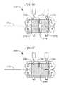
- FIG. 14is a side schematic view of an eleventh alternative embodiment scan test apparatus
- FIG. 15is a side schematic view of a twelfth alternative embodiment scan test apparatus
- FIG. 16is a side schematic view of a thirteenth alternative embodiment scan test apparatus.
- FIG. 17is a side schematic view of a fourteenth alternative embodiment scan test apparatus.
- FIGS. 18–20are schematic software flow diagrams illustrating continuity, isolation and proper test modules.
- FIG. 1One embodiment of a scan test apparatus 10 of U.S. Pat. No. 6,191,600 B1 is shown in FIG. 1 .
- This scan test apparatusincludes an upper shorting layer 12 and a lower shorting layer 14 which during testing sandwiches the printed circuit board to be tested or unit under test 16 .
- the upper shorting layercomprises an inner conductive layer 18 such as conductive cloth or metal and an outer compliant layer 20 such as foam.
- the lower shorting layerhas an inner conductive layer 22 and an outer compliant layer 24 made of the same materials as the upper shorting layer.
- the upper shorting layer 12 and the lower shorting layer 14can consist of a single material which is both conductive and compliant such as conductive rubber.
- each wiper brushis wired to discrete switches 27 in a printed circuit board 28 .
- the printed circuit board 28is connected to measurement electronics 30 by a cable 32 .
- the upper and lower shorting layersmust contact the entire unit under test except for the row of wiper brushes which is wider than the width of the unit under test. If a row of wiper brushes is located in both the upper and lower shorting layers, they must be offset from one another so as not to contact the unit under test at the same location along the length of the board.
- the unit under test 16is sandwiched between the upper and lower shorting layers which shorts out both sides of the unit under test by an electrical current introduced into the conductive layers of the shorting layers. With a shorting current introduced into the unit under test, it is pushed underneath the wiper brushes 26 by a push rod 34 .
- Push rod 34is actuated by a pneumatic cylinder, a hydraulic cylinder or a linear motor 36 .
- the unit under test 16includes numerous test pads connected by traces, such as for example test pads 38 and 40 connected by trace 39 , as shown in FIG. 2 a. As shown in FIGS. 2 a through 2 d, as the unit under test 16 passes beneath the wiper brushes 26 individual test pads 38 and 40 , if properly connected and carrying a current, will turn on the individual wiper brushes contacting the test pads. The turned on wiper brushes will send a signal to the measurement electronics which will generate a first test image 42 and 44 for test pads 38 and 40 by software programmed into the measurement electronics. Individual test pads on the unit under test will vary in size and may not coincide with the exact width of adjacent wiper brushes.
- first test images 42 and 44 generatedwill coincide with the width of the wiper brushes turned on by the test pads which may not be the exact physical dimension of the test pad itself.
- First test images 42 and 44are generated when the unit under test is passed beneath the wiper brushes in direction 46 . Since the first test image may be larger than the actual test pads, the unit under test is rotated 90° and passed beneath the wiper brushes a second time in direction 48 . As the wiper brushes contact the test pads 38 and 40 for the second time, they will generate a second test image 50 and 52 corresponding to a second dimension of the test pads.
- the software for the measurement electronicsthen superimposes the second test image upon the first test image as shown in FIG.
- a final test image 54 and 56which is the area of overlap between the first and second test images corresponding to test pads 38 and 40 .
- the final test imageis then compared to net list data or test pad data contained within the software.
- the softwarecompares the stored data with the scanned data and if they match, the software eliminates those test pads from subsequent continuity testing to be done by conventional means such as by a prober.
- test pads 38 and 40If, for example, trace 39 was broken and did not properly electrically connect test pads 38 and 40 , the wiper brushes would not have been able to generate the necessary final test image and the software would identify test pads 38 and 40 as potential problem areas needing further continuity testing by a prober.
- the scan test apparatuseliminates test points from further continuity testing by electrically scanning the circuit board and looking for what is properly electrically connected in the circuit. By eliminating what is properly electrically connected, 80 to 90% of all test pads can be eliminated from testing by conventional methods.
- the scan test apparatussignificantly reduces the time necessary to perform continuity testing on bare printed circuit boards.
- FIG. 3illustrates an alternative embodiment scan testing apparatus 60 of U.S. Pat. No. 6,191,600 B1.
- the upper and lower shorting layers 12 and 14are formed in a continuous loop around rollers 62 which are driven by a motor 64 .
- the unit under test 16is driven past the wiper brushes by the upper and lower shorting layers to generate the test images.
- FIG. 4illustrates a scan test apparatus 100 for double-sided scanning of a printed circuit board 102 .
- Apparatus 100includes upper housing 104 and lower housing 106 between which the printed circuit board is passed.
- Upper housing 104includes a forward electrical contactor 108 and a rear electrical contactor 110 positioned on either side of a shorting matrix 112 .
- lower housing 106includes forward electrical contactor 114 and rear electrical contactor 116 positioned on either side of a shorting matrix 118 .
- Upper housing 104includes forward and rear drive rollers 120 and 122 , which cooperate with forward and rear drive rollers 124 , 126 attached to lower housing 106 .
- lower housingwould be rigidly connected to a base and upper housing would be biased toward the lower housing by actuators 128 .
- the actuatorscould be a linear motor, a pneumatic or hydraulic cylinder, or a spring.
- the printed circuit boardis scanned by the drive rollers, which are geared and driven by a motor, drawing the printed circuit board through the forward electrical actuators, the shorting matrix and the rear electrical contactors and ultimately out of the scan test apparatus through the rear drive rollers.
- the electrical contactorscan be wiper brushes or test probes, such as accordion probes, beam probes, or flex circuit fingers.
- the shorting matrixcan be a conductive and compliant layer as shown in FIG. 1 or can be a metal plate.
- FIG. 5shows another alternative embodiment scan test apparatus 130 for single-sided scanning. This embodiment is similar to FIG. 4 , except the forward and rear electrical contactors 114 , 116 and shorting matrix 118 in the lower housing 106 has been replaced with additional drive rollers 132 and 134 . This embodiment would be used when only one side of the printed circuit board requires testing.
- FIG. 6illustrates another embodiment scan test apparatus 140 where the printed circuit board 102 would be held stationary by mounting chucks 142 and 144 positioned on either side of the printed circuit board.
- the drive rollers 120 and 122 of upper housing 104traverse a fixed rail 146 .
- drive rollers 124 and 126 of lower housing 106ride on a lower rail 148 .
- Scan test apparatus 140includes electrical contactors and shorting matrix positioned on the upper and lower housings similar to scan test apparatus 100 of FIG. 4 for double-sided scanning of the printed circuit board 102 .
- FIG. 7illustrates yet another embodiment scan test apparatus 150 wherein the printed circuit board 102 is held stationary for single-sided scanning.
- the printed circuit boardis held stationary by a vacuum or mounting plate 152 .
- the scan test apparatus 150includes a lower housing 106 having drive rollers 124 and 126 which ride on rail 148 .
- electrical contactors 114 and 116are positioned on either side of the shorting matrix 118 .
- FIG. 7illustrates single-sided scanning for the lower surface of the printed circuit board 102 , it is to be understood that the top surface of the printed circuit board similarly could be scanned in one-sided scanning utilizing only the upper portion of scan test apparatus 140 .
- FIG. 8shows yet another embodiment scan test apparatus 160 wherein the electrical contactors 162 and 164 positioned in upper housing 104 and lower housing 106 , respectively, perform a double-sided charge rise time (CRT) measurement.
- CRT measurementmeasures the capacitance build-up in nets on the printed circuit board.
- This scan test apparatus 160includes non-contact measurements of capacitance, forced modulation microscopy, phase detection microscopy, electrostatic force microscopy, scanning capacitance microscopy, scanning thermal microscopy, near-field scanning optical microscopy, nanolithography, pulsed force mode, micro-thermal analysis, conductive AFM, E-beam technology, plasma charge and laser beam.
- FIG. 9illustrates another scan test apparatus 170 similar to scan test apparatus 160 , which provides single-sided CRT measurement.
- a single electrical contactor 172is positioned on either the upper housing 104 or lower housing 106 , depending upon the side of the printed circuit board requiring testing.
- FIG. 10illustrates another scan test apparatus 180 which performs single-sided scanning on the printed circuit board 102 .
- the scan test apparatus 180includes an upper housing 104 with drive rollers, 120 and 122 .
- An electrical contactor 182is positioned between the drive rollers.
- Located below the printed circuit boardare three drive rollers 184 , 186 and 188 having a conductive belt or cloth 190 which serves as a shorting matrix for the printed circuit board.
- FIG. 11illustrates an alternative embodiment scan test apparatus 192 similar to FIG. 6 , with the exception that the housing and drive roller assemblies have been replaced with motion units 194 and 196 .
- These motions unitscan be a linear motor, pneumatic or hydraulic cylinders which move together for double-sided scanning of the printed circuit board.
- FIG. 12illustrates a scan test apparatus 200 similar to FIG. 7 wherein the housing and drive roller assembly is replaced with a motion unit 202 as shown in FIG. 11 .
- the scan test apparatus 200is used for single-sided scanning of the printed circuit board. Again, this embodiment can be used for scanning either side of the printed circuit board as required.
- FIG. 13illustrates a scan test apparatus 210 , including a motion unit 212 and an electrical contactor 214 for single-sided scanning of the printed circuit board 102 .
- the printed circuit board 102is held stationary by the shorting vacuum plate or mounting plate 216 .
- FIG. 14illustrates a scan test apparatus 220 , including an upper housing 222 and a lower housing 224 .
- Upper housing 222includes drive rollers 226 and 228
- lower housing 224includes drive rollers 230 and 232 .
- Each of upper housing 222 and lower housing 224includes an array of electrical contactors 234 and 236 , respectively.
- Scan test apparatus 220performs double-sided scanning wherein the electrical contactor array is used for selective shorting and measurement.
- the solid array of contactors 234 and 236selectively measure and short combinations of areas of the printed circuit board 102 in order to achieve the desired measurements.
- Scan test apparatus 220also includes actuators 238 to bias the upper and lower housings towards one another.
- FIG. 15illustrates another alternative embodiment scan test apparatus 250 for double-sided scan testing having non-contact sensors.
- Apparatus 250includes upper housing 252 and lower housing 254 . Each of the upper and lower housing has a forward drive roller 256 and a rear drive roller 258 .
- Upper and lower shorting matrixes 260 and 262are connected to the upper and lower housings, respectively.
- Leading non-contact sensors 264 and rear non-contact sensors 266are positioned adjacent the shorting matrixes 260 and 262 .
- Upper and lower housingsare biased by actuators 268 .
- FIG. 16illustrates another alternative embodiment scan test apparatus 270 having one non-contact sensor 272 positioned above and below the printed circuit board 102 for double-sided non-contact scanning.
- Shorting matrix 276is positioned on either side of the upper and lower non-contact sensors 272 and 274 .
- FIG. 17illustrates another embodiment scan test apparatus 280 for single-sided non-contact scanning having one non-contact sensor 282 positioned on one side of the printed circuit board and having shorting matrix 284 positioned on either side of the sensor.
- Shorting matrix 286is positioned on the opposite side of the printed circuit board 102 .
- Scan test apparatus 280could incorporate only shorting matrix 286 or only shorting matrixes 284 with additional drive rollers on the lower housing.
- the electrical contactorseach may be connected to the test electronics through separate switches or can be connected directly to measurement circuits.
- a decoder cardcould be used to filter out measurement noise before evaluating the signals using a measurement board for the scan test apparatus.
- the embodiments of the present inventiondo not require that the entire board be shorted simultaneously and can be programmed depending upon the requirements of the printed circuit board under test.
- the scan test apparatusalso can be programmed to be self-learning without the use of control data. Any embodiments utilizing CRT can perform a 100% test without the need for the use of an additional prober.
- the scan test apparatus of the present inventionperforms a continuity test wherein the board data is first accessed and aligned to match the board positions within a reasonable tolerance. Based on user settings for desirable test thresholds, ADAC is programmed with a comparison voltage for pass/fail results. Next, the board is moved under two sets of electrical contactors (leading and trailing sets, each set consisting of a row of contacts on a top and bottom of the unit under test) and a grounding plate in such a manner as to synchronize the position of the board with the measurement system. The measurement system stimulates each contact or group of contacts with a known voltage through a load resistor, the pads and networks on the unit under test and eventually the ground plate.
- the voltage and the contactis compared via hardware to the comparison voltage and the result is stored for analysis. This is repeated multiple times for each pad to allow contact redundancy and positionable tolerance.
- the data from the contactsis combined with a second sweep at 90° rotation to maximum coverage on complex networks.
- the resultsare compared to the expected values and used to eliminate nets from the final prober test section.
- the isolation test module shown in FIG. 19the board data is first accessed and aligned to match the board position within a reasonable tolerance. All possible test locations are analyzed and a limited number of optimal locations are selected to tested the maximum number of networks and the fewest number of movements. The board is moved under a single set of context (upper and lower) to pre-calculated test positions.
- the scan test apparatusthen conducts a proper test module wherein the board data is first accessed and aligned to match the board position within a reasonable tolerance.
- the unverified and failed pads from the continuity test module and the unverified and failed networks from the isolation test modulesare then tested on the prober module and the final test results (pass or fail) is applied to the finished board.
Landscapes
- Engineering & Computer Science (AREA)
- Microelectronics & Electronic Packaging (AREA)
- Computer Hardware Design (AREA)
- General Engineering & Computer Science (AREA)
- Physics & Mathematics (AREA)
- General Physics & Mathematics (AREA)
- Manufacturing & Machinery (AREA)
- Tests Of Electronic Circuits (AREA)
- Testing Of Short-Circuits, Discontinuities, Leakage, Or Incorrect Line Connections (AREA)
- Measuring Leads Or Probes (AREA)
- Investigating Or Analyzing Materials By The Use Of Electric Means (AREA)
Abstract
Description
Claims (2)
Priority Applications (1)
| Application Number | Priority Date | Filing Date | Title |
|---|---|---|---|
| US10/897,182US7071716B2 (en) | 2001-11-16 | 2004-07-22 | Apparatus for scan testing printed circuit boards |
Applications Claiming Priority (2)
| Application Number | Priority Date | Filing Date | Title |
|---|---|---|---|
| US09/991,199US6788078B2 (en) | 2001-11-16 | 2001-11-16 | Apparatus for scan testing printed circuit boards |
| US10/897,182US7071716B2 (en) | 2001-11-16 | 2004-07-22 | Apparatus for scan testing printed circuit boards |
Related Parent Applications (1)
| Application Number | Title | Priority Date | Filing Date |
|---|---|---|---|
| US09/991,199DivisionUS6788078B2 (en) | 2001-11-16 | 2001-11-16 | Apparatus for scan testing printed circuit boards |
Publications (2)
| Publication Number | Publication Date |
|---|---|
| US20050001640A1 US20050001640A1 (en) | 2005-01-06 |
| US7071716B2true US7071716B2 (en) | 2006-07-04 |
Family
ID=25536973
Family Applications (2)
| Application Number | Title | Priority Date | Filing Date |
|---|---|---|---|
| US09/991,199Expired - Fee RelatedUS6788078B2 (en) | 2001-11-16 | 2001-11-16 | Apparatus for scan testing printed circuit boards |
| US10/897,182Expired - Fee RelatedUS7071716B2 (en) | 2001-11-16 | 2004-07-22 | Apparatus for scan testing printed circuit boards |
Family Applications Before (1)
| Application Number | Title | Priority Date | Filing Date |
|---|---|---|---|
| US09/991,199Expired - Fee RelatedUS6788078B2 (en) | 2001-11-16 | 2001-11-16 | Apparatus for scan testing printed circuit boards |
Country Status (9)
| Country | Link |
|---|---|
| US (2) | US6788078B2 (en) |
| EP (1) | EP1312930B1 (en) |
| JP (2) | JP2003227860A (en) |
| KR (1) | KR100560089B1 (en) |
| CN (1) | CN1220067C (en) |
| AT (1) | ATE352043T1 (en) |
| DE (1) | DE60217619T2 (en) |
| SG (1) | SG114583A1 (en) |
| TW (1) | TWI252926B (en) |
Cited By (3)
| Publication number | Priority date | Publication date | Assignee | Title |
|---|---|---|---|---|
| US20100117671A1 (en)* | 2008-11-12 | 2010-05-13 | Optisolar, Inc. | Simulated mounting structure for testing electrical devices |
| US20110095766A1 (en)* | 2009-10-28 | 2011-04-28 | Infinitum Solutions, Inc. | Testing flex and apfa assemblies for hard disk drives |
| US20150077151A1 (en)* | 2013-09-13 | 2015-03-19 | Infineon Technologies Ag | Apparatus and Method for Testing Electric Conductors |
Families Citing this family (8)
| Publication number | Priority date | Publication date | Assignee | Title |
|---|---|---|---|---|
| US6788078B2 (en)* | 2001-11-16 | 2004-09-07 | Delaware Capital Formation, Inc. | Apparatus for scan testing printed circuit boards |
| US7519496B2 (en)* | 2003-09-19 | 2009-04-14 | Nxp B.V. | Electronic circuit comprising a secret sub-module |
| US7364475B2 (en)* | 2004-12-22 | 2008-04-29 | Spectra Logic Corporation | Spring based continuity alignment apparatus and method |
| US7353479B2 (en)* | 2005-01-31 | 2008-04-01 | Faraday Technology Corp. | Method for placing probing pad and computer readable recording medium for storing program thereof |
| DE102009004555A1 (en) | 2009-01-14 | 2010-09-30 | Atg Luther & Maelzer Gmbh | Method for testing printed circuit boards |
| US8742777B2 (en) | 2010-12-29 | 2014-06-03 | The Board Of Trustees Of The University Of Alabama For And On Behalf Of The University Of Alabama | Method and system for testing an electric circuit |
| CN107526027B (en)* | 2017-09-04 | 2019-08-20 | 中国航空工业集团公司洛阳电光设备研究所 | A kind of PCBA board bga chip solder joint problem fast diagnosis method |
| CN114665984B (en)* | 2022-02-28 | 2024-07-30 | 歌尔股份有限公司 | Test device |
Citations (56)
| Publication number | Priority date | Publication date | Assignee | Title |
|---|---|---|---|---|
| US3629702A (en) | 1970-03-09 | 1971-12-21 | Hazeltine Corp | Automatic tester for a plurality of discrete electrical components supplied in a repetitive predetermined sequence |
| JPS5827784U (en) | 1981-08-18 | 1983-02-22 | 富士通株式会社 | Probe fixing jig |
| EP0128107A1 (en) | 1983-05-04 | 1984-12-12 | Optrotech Ltd. | Apparatus and method for automatic inspection of printed circuit boards |
| GB2149130A (en) | 1983-10-28 | 1985-06-05 | Int Computers Ltd | Testing electronic circuits |
| JPS61274278A (en) | 1985-05-30 | 1986-12-04 | Nec Corp | Continuity measuring jig for substrate |
| JPS62285072A (en) | 1986-06-04 | 1987-12-10 | Hitachi Ltd | Wire pattern inspecting device for printed circuit board |
| JPS6390173U (en) | 1986-12-02 | 1988-06-11 | ||
| JPS63157675U (en) | 1987-04-03 | 1988-10-17 | ||
| US4818933A (en) | 1986-10-08 | 1989-04-04 | Hewlett-Packard Company | Board fixturing system |
| US4836797A (en) | 1986-12-16 | 1989-06-06 | Sym-Tek Systems, Inc. | Electrical device contactor |
| JPH022946A (en) | 1988-06-17 | 1990-01-08 | Kyoei Seigyo Kiki Kk | Conduction detecting method for electronic circuit wire |
| JPH0213862A (en) | 1988-06-30 | 1990-01-18 | Fujitsu Ltd | Printed circuit board inspection equipment |
| JPH02130483A (en) | 1988-11-11 | 1990-05-18 | Teru Tohoku Kk | Inspecting method of printed circuit board |
| US4970461A (en) | 1989-06-26 | 1990-11-13 | Lepage Andrew J | Method and apparatus for non-contact opens/shorts testing of electrical circuits |
| EP0424270A2 (en) | 1989-10-20 | 1991-04-24 | Digital Equipment Corporation | Electro-emissive laser stimulated test |
| JPH03152481A (en) | 1989-11-09 | 1991-06-28 | Nec Corp | Flying probe head |
| US5094584A (en) | 1989-04-06 | 1992-03-10 | Hewlett-Packard Company | Method and apparatus for automatically changing printed circuit board test fixtures |
| US5113133A (en) | 1990-12-20 | 1992-05-12 | Integri-Test Corporation | Circuit board test probe |
| US5124660A (en) | 1990-12-20 | 1992-06-23 | Hewlett-Packard Company | Identification of pin-open faults by capacitive coupling through the integrated circuit package |
| US5138266A (en) | 1989-10-20 | 1992-08-11 | Digital Equipment Corporation | Single-probe charge measurement testing method |
| JPH04259862A (en) | 1991-02-15 | 1992-09-16 | Fujitsu Ltd | Printed circuit board testing equipment |
| JPH0446217Y2 (en) | 1987-11-30 | 1992-10-29 | ||
| JPH04127576U (en) | 1991-05-10 | 1992-11-20 | 大西電子株式会社 | Conductive head for circuit inspection of printed wiring boards |
| US5202623A (en) | 1992-02-26 | 1993-04-13 | Digital Equipment Corporation | Laser-activated plasma chamber for non-contact testing |
| GB2265224A (en) | 1992-03-20 | 1993-09-22 | Centalic Tech Dev Ltd | Testing printed circuit boards |
| JPH05273305A (en) | 1992-03-24 | 1993-10-22 | Tescon:Kk | Inspecting device for printed-circuit board |
| US5268645A (en) | 1991-04-10 | 1993-12-07 | Atg Electronic Gmbh | Method of and apparatus for testing circuit boards and the like with an inhomogeneous electric field |
| US5270643A (en) | 1990-11-28 | 1993-12-14 | Schlumberger Technologies | Pulsed laser photoemission electron-beam probe |
| GB2267970A (en) | 1992-06-11 | 1993-12-22 | Northern Telecom Ltd | Testing unpopulated printed circuit boards |
| JPH0611498Y2 (en) | 1988-02-26 | 1994-03-23 | 日本電気株式会社 | Address translator |
| US5369431A (en) | 1992-02-25 | 1994-11-29 | Orbotech | Verification and repair station of PCBS |
| JPH0783954A (en) | 1993-09-13 | 1995-03-31 | Toshiba Corp | Wiring board inspection machine |
| JPH0792227A (en) | 1993-09-24 | 1995-04-07 | Toyota Motor Corp | Circuit board inspection apparatus and inspection method |
| JPH07151834A (en) | 1993-09-15 | 1995-06-16 | Hewlett Packard Co <Hp> | Inspection system for electronic assembly using robot-type positioning of probe |
| JPH0815361A (en) | 1994-06-30 | 1996-01-19 | Matsushita Electric Works Ltd | Inspection method for printed wiring board |
| US5493236A (en) | 1993-06-23 | 1996-02-20 | Mitsubishi Denki Kabushiki Kaisha | Test analysis apparatus and analysis method for semiconductor wafer using OBIC analysis |
| US5506510A (en) | 1994-05-18 | 1996-04-09 | Genrad, Inc. | Adaptive alignment probe fixture for circuit board tester |
| US5508627A (en) | 1994-05-11 | 1996-04-16 | Patterson; Joseph M. | Photon assisted sub-tunneling electrical probe, probe tip, and probing method |
| US5517110A (en) | 1995-04-06 | 1996-05-14 | Yentec Inc. | Contactless test method and system for testing printed circuit boards |
| JPH08189939A (en) | 1995-01-10 | 1996-07-23 | Iwaki Electron Corp Ltd | Probing characteristic testing device |
| WO1996026446A1 (en) | 1995-02-23 | 1996-08-29 | Aesop, Inc. | Manipulator for automatic test equipment test head |
| US5553700A (en) | 1995-04-10 | 1996-09-10 | Atotech Usa, Inc. | Treatment method and apparatus for printed circuit boards and the like |
| EP0731360A2 (en) | 1995-02-28 | 1996-09-11 | Plessey Semiconductors Limited | Structure for testing bare integrated circuit devices |
| US5587664A (en) | 1995-07-12 | 1996-12-24 | Exsight Ltd. | Laser-induced metallic plasma for non-contact inspection |
| EP0773445A2 (en) | 1995-11-10 | 1997-05-14 | OHT Inc. | Inspection apparatus of conductive patterns |
| US5729146A (en) | 1995-09-21 | 1998-03-17 | Everett Charles Technologies, Inc. | Quick stacking translator fixture |
| US5771144A (en) | 1995-03-31 | 1998-06-23 | Daewoo Electronics Co., Ltd. | Cleaning device for a contact surface of a printed circuit board |
| US5773988A (en) | 1996-10-29 | 1998-06-30 | Hewlett-Packard Company | Standard- and limited-access hybrid test fixture |
| EP0884596A2 (en) | 1997-05-13 | 1998-12-16 | Nidec-Read Corporation | Circuit board misalignment detection apparatus and method |
| DE19730516A1 (en) | 1997-07-03 | 1999-01-07 | Luther & Maelzer Gmbh | PCB tester |
| US6145648A (en) | 1997-01-24 | 2000-11-14 | Orbotech Ltd. | Method and system for continuously processing successive workpieces along a production line |
| EP1059538A2 (en) | 1999-05-31 | 2000-12-13 | Nihon Densan Read Kabushiki Kaisha, (Nidec-Read Corporation) | Printed circuit board testing apparatus |
| US6191600B1 (en) | 1999-01-22 | 2001-02-20 | Delaware Capital Formation, Inc. | Scan test apparatus for continuity testing of bare printed circuit boards |
| US6268719B1 (en) | 1998-09-23 | 2001-07-31 | Delaware Capital Formation, Inc. | Printed circuit board test apparatus |
| US6572396B1 (en) | 1999-02-02 | 2003-06-03 | Gryphics, Inc. | Low or zero insertion force connector for printed circuit boards and electrical devices |
| US6788078B2 (en)* | 2001-11-16 | 2004-09-07 | Delaware Capital Formation, Inc. | Apparatus for scan testing printed circuit boards |
Family Cites Families (1)
| Publication number | Priority date | Publication date | Assignee | Title |
|---|---|---|---|---|
| JP2878033B2 (en) | 1992-07-24 | 1999-04-05 | 日本電気株式会社 | Switching system of subscriber transmission line |
- 2001
- 2001-11-16USUS09/991,199patent/US6788078B2/ennot_activeExpired - Fee Related
- 2002
- 2002-11-12ATAT02025085Tpatent/ATE352043T1/enactive
- 2002-11-12DEDE60217619Tpatent/DE60217619T2/ennot_activeExpired - Lifetime
- 2002-11-12EPEP02025085Apatent/EP1312930B1/ennot_activeExpired - Lifetime
- 2002-11-15KRKR1020020071079Apatent/KR100560089B1/ennot_activeExpired - Fee Related
- 2002-11-15SGSG200206891Apatent/SG114583A1/enunknown
- 2002-11-15CNCNB021602344Apatent/CN1220067C/ennot_activeExpired - Fee Related
- 2002-11-15TWTW091133527Apatent/TWI252926B/ennot_activeIP Right Cessation
- 2002-11-15JPJP2002332366Apatent/JP2003227860A/ennot_activeWithdrawn
- 2004
- 2004-07-22USUS10/897,182patent/US7071716B2/ennot_activeExpired - Fee Related
- 2007
- 2007-02-28JPJP2007050715Apatent/JP2007256277A/enactivePending
Patent Citations (62)
| Publication number | Priority date | Publication date | Assignee | Title |
|---|---|---|---|---|
| US3629702A (en) | 1970-03-09 | 1971-12-21 | Hazeltine Corp | Automatic tester for a plurality of discrete electrical components supplied in a repetitive predetermined sequence |
| JPS5827784U (en) | 1981-08-18 | 1983-02-22 | 富士通株式会社 | Probe fixing jig |
| EP0128107A1 (en) | 1983-05-04 | 1984-12-12 | Optrotech Ltd. | Apparatus and method for automatic inspection of printed circuit boards |
| JPS6046470A (en) | 1983-05-04 | 1985-03-13 | オプトロテツク リミテツド | Inspection device for printed circuit substrate |
| GB2149130A (en) | 1983-10-28 | 1985-06-05 | Int Computers Ltd | Testing electronic circuits |
| JPS61274278A (en) | 1985-05-30 | 1986-12-04 | Nec Corp | Continuity measuring jig for substrate |
| JPS62285072A (en) | 1986-06-04 | 1987-12-10 | Hitachi Ltd | Wire pattern inspecting device for printed circuit board |
| US4818933A (en) | 1986-10-08 | 1989-04-04 | Hewlett-Packard Company | Board fixturing system |
| JPS6390173U (en) | 1986-12-02 | 1988-06-11 | ||
| US4836797A (en) | 1986-12-16 | 1989-06-06 | Sym-Tek Systems, Inc. | Electrical device contactor |
| JPS63157675U (en) | 1987-04-03 | 1988-10-17 | ||
| JPH0446217Y2 (en) | 1987-11-30 | 1992-10-29 | ||
| JPH0611498Y2 (en) | 1988-02-26 | 1994-03-23 | 日本電気株式会社 | Address translator |
| JPH022946A (en) | 1988-06-17 | 1990-01-08 | Kyoei Seigyo Kiki Kk | Conduction detecting method for electronic circuit wire |
| JPH0213862A (en) | 1988-06-30 | 1990-01-18 | Fujitsu Ltd | Printed circuit board inspection equipment |
| JPH02130483A (en) | 1988-11-11 | 1990-05-18 | Teru Tohoku Kk | Inspecting method of printed circuit board |
| US5094584A (en) | 1989-04-06 | 1992-03-10 | Hewlett-Packard Company | Method and apparatus for automatically changing printed circuit board test fixtures |
| US4970461A (en) | 1989-06-26 | 1990-11-13 | Lepage Andrew J | Method and apparatus for non-contact opens/shorts testing of electrical circuits |
| JPH03206983A (en) | 1989-10-20 | 1991-09-10 | Digital Equip Corp <Dec> | Test for stimulating electron emission laser |
| EP0424270A3 (en) | 1989-10-20 | 1991-09-11 | Digital Equipment Corporation | Electro-emissive laser stimulated test |
| US5138266A (en) | 1989-10-20 | 1992-08-11 | Digital Equipment Corporation | Single-probe charge measurement testing method |
| US5017863A (en) | 1989-10-20 | 1991-05-21 | Digital Equipment Corporation | Electro-emissive laser stimulated test |
| EP0424270A2 (en) | 1989-10-20 | 1991-04-24 | Digital Equipment Corporation | Electro-emissive laser stimulated test |
| JPH03152481A (en) | 1989-11-09 | 1991-06-28 | Nec Corp | Flying probe head |
| US5270643A (en) | 1990-11-28 | 1993-12-14 | Schlumberger Technologies | Pulsed laser photoemission electron-beam probe |
| US5113133A (en) | 1990-12-20 | 1992-05-12 | Integri-Test Corporation | Circuit board test probe |
| US5124660A (en) | 1990-12-20 | 1992-06-23 | Hewlett-Packard Company | Identification of pin-open faults by capacitive coupling through the integrated circuit package |
| JPH04259862A (en) | 1991-02-15 | 1992-09-16 | Fujitsu Ltd | Printed circuit board testing equipment |
| US5268645A (en) | 1991-04-10 | 1993-12-07 | Atg Electronic Gmbh | Method of and apparatus for testing circuit boards and the like with an inhomogeneous electric field |
| JPH04127576U (en) | 1991-05-10 | 1992-11-20 | 大西電子株式会社 | Conductive head for circuit inspection of printed wiring boards |
| US5469064A (en) | 1992-01-14 | 1995-11-21 | Hewlett-Packard Company | Electrical assembly testing using robotic positioning of probes |
| US5369431A (en) | 1992-02-25 | 1994-11-29 | Orbotech | Verification and repair station of PCBS |
| US5202623A (en) | 1992-02-26 | 1993-04-13 | Digital Equipment Corporation | Laser-activated plasma chamber for non-contact testing |
| GB2265224A (en) | 1992-03-20 | 1993-09-22 | Centalic Tech Dev Ltd | Testing printed circuit boards |
| JPH05273305A (en) | 1992-03-24 | 1993-10-22 | Tescon:Kk | Inspecting device for printed-circuit board |
| GB2267970A (en) | 1992-06-11 | 1993-12-22 | Northern Telecom Ltd | Testing unpopulated printed circuit boards |
| US5493236A (en) | 1993-06-23 | 1996-02-20 | Mitsubishi Denki Kabushiki Kaisha | Test analysis apparatus and analysis method for semiconductor wafer using OBIC analysis |
| JPH0783954A (en) | 1993-09-13 | 1995-03-31 | Toshiba Corp | Wiring board inspection machine |
| JPH07151834A (en) | 1993-09-15 | 1995-06-16 | Hewlett Packard Co <Hp> | Inspection system for electronic assembly using robot-type positioning of probe |
| JPH0792227A (en) | 1993-09-24 | 1995-04-07 | Toyota Motor Corp | Circuit board inspection apparatus and inspection method |
| US5508627A (en) | 1994-05-11 | 1996-04-16 | Patterson; Joseph M. | Photon assisted sub-tunneling electrical probe, probe tip, and probing method |
| US5506510A (en) | 1994-05-18 | 1996-04-09 | Genrad, Inc. | Adaptive alignment probe fixture for circuit board tester |
| JPH0815361A (en) | 1994-06-30 | 1996-01-19 | Matsushita Electric Works Ltd | Inspection method for printed wiring board |
| JPH08189939A (en) | 1995-01-10 | 1996-07-23 | Iwaki Electron Corp Ltd | Probing characteristic testing device |
| WO1996026446A1 (en) | 1995-02-23 | 1996-08-29 | Aesop, Inc. | Manipulator for automatic test equipment test head |
| EP0731360A2 (en) | 1995-02-28 | 1996-09-11 | Plessey Semiconductors Limited | Structure for testing bare integrated circuit devices |
| EP0731360A3 (en) | 1995-02-28 | 1997-07-16 | Plessey Semiconductors Ltd | Construction to test bare integrated circuits |
| US5771144A (en) | 1995-03-31 | 1998-06-23 | Daewoo Electronics Co., Ltd. | Cleaning device for a contact surface of a printed circuit board |
| US5517110A (en) | 1995-04-06 | 1996-05-14 | Yentec Inc. | Contactless test method and system for testing printed circuit boards |
| US5553700A (en) | 1995-04-10 | 1996-09-10 | Atotech Usa, Inc. | Treatment method and apparatus for printed circuit boards and the like |
| US5587664A (en) | 1995-07-12 | 1996-12-24 | Exsight Ltd. | Laser-induced metallic plasma for non-contact inspection |
| US5729146A (en) | 1995-09-21 | 1998-03-17 | Everett Charles Technologies, Inc. | Quick stacking translator fixture |
| EP0773445A2 (en) | 1995-11-10 | 1997-05-14 | OHT Inc. | Inspection apparatus of conductive patterns |
| US5773988A (en) | 1996-10-29 | 1998-06-30 | Hewlett-Packard Company | Standard- and limited-access hybrid test fixture |
| US6145648A (en) | 1997-01-24 | 2000-11-14 | Orbotech Ltd. | Method and system for continuously processing successive workpieces along a production line |
| EP0884596A2 (en) | 1997-05-13 | 1998-12-16 | Nidec-Read Corporation | Circuit board misalignment detection apparatus and method |
| DE19730516A1 (en) | 1997-07-03 | 1999-01-07 | Luther & Maelzer Gmbh | PCB tester |
| US6268719B1 (en) | 1998-09-23 | 2001-07-31 | Delaware Capital Formation, Inc. | Printed circuit board test apparatus |
| US6191600B1 (en) | 1999-01-22 | 2001-02-20 | Delaware Capital Formation, Inc. | Scan test apparatus for continuity testing of bare printed circuit boards |
| US6572396B1 (en) | 1999-02-02 | 2003-06-03 | Gryphics, Inc. | Low or zero insertion force connector for printed circuit boards and electrical devices |
| EP1059538A2 (en) | 1999-05-31 | 2000-12-13 | Nihon Densan Read Kabushiki Kaisha, (Nidec-Read Corporation) | Printed circuit board testing apparatus |
| US6788078B2 (en)* | 2001-11-16 | 2004-09-07 | Delaware Capital Formation, Inc. | Apparatus for scan testing printed circuit boards |
Non-Patent Citations (2)
| Title |
|---|
| Degroat, P.M. et al., "Finding Shorts in Printed Circuit Boards," IBM Technical Disclosure Bulletin, vol. 12, No. 5, Oct. 1969, pp. 655-656. |
| Japanese Patent Abstract: Publication No. 02-259478, Publication Date Oct. 22, 1990; 2 pages. |
Cited By (6)
| Publication number | Priority date | Publication date | Assignee | Title |
|---|---|---|---|---|
| US20100117671A1 (en)* | 2008-11-12 | 2010-05-13 | Optisolar, Inc. | Simulated mounting structure for testing electrical devices |
| US8305105B2 (en)* | 2008-11-12 | 2012-11-06 | Novasolar Holdings Limited | Simulated mounting structure for testing electrical devices |
| US20110095766A1 (en)* | 2009-10-28 | 2011-04-28 | Infinitum Solutions, Inc. | Testing flex and apfa assemblies for hard disk drives |
| US8536875B2 (en)* | 2009-10-28 | 2013-09-17 | Infinitum Solutions, Inc. | Testing flex and APFA assemblies for hard disk drives |
| US20150077151A1 (en)* | 2013-09-13 | 2015-03-19 | Infineon Technologies Ag | Apparatus and Method for Testing Electric Conductors |
| US9523729B2 (en)* | 2013-09-13 | 2016-12-20 | Infineon Technologies Ag | Apparatus and method for testing electric conductors |
Also Published As
| Publication number | Publication date |
|---|---|
| JP2003227860A (en) | 2003-08-15 |
| JP2007256277A (en) | 2007-10-04 |
| TWI252926B (en) | 2006-04-11 |
| CN1438491A (en) | 2003-08-27 |
| US20050001640A1 (en) | 2005-01-06 |
| DE60217619T2 (en) | 2007-10-11 |
| KR20030041094A (en) | 2003-05-23 |
| US20030094961A1 (en) | 2003-05-22 |
| US6788078B2 (en) | 2004-09-07 |
| TW200300846A (en) | 2003-06-16 |
| HK1056218A1 (en) | 2004-02-06 |
| SG114583A1 (en) | 2005-09-28 |
| ATE352043T1 (en) | 2007-02-15 |
| DE60217619D1 (en) | 2007-03-08 |
| EP1312930A3 (en) | 2004-03-17 |
| KR100560089B1 (en) | 2006-03-10 |
| EP1312930A2 (en) | 2003-05-21 |
| CN1220067C (en) | 2005-09-21 |
| EP1312930B1 (en) | 2007-01-17 |
Similar Documents
| Publication | Publication Date | Title |
|---|---|---|
| US5469064A (en) | Electrical assembly testing using robotic positioning of probes | |
| JP2007256277A (en) | Apparatus for scan testing printed circuit board | |
| US6727712B2 (en) | Apparatus and methods for testing circuit boards | |
| US6268719B1 (en) | Printed circuit board test apparatus | |
| KR100526744B1 (en) | Machine for the electric test of printed circuits | |
| US20010015641A1 (en) | Circuit board testing apparatus | |
| US6191600B1 (en) | Scan test apparatus for continuity testing of bare printed circuit boards | |
| EP0989409A1 (en) | Scan test machine for densely spaced test sites | |
| EP1415166B1 (en) | Apparatus and method for testing bare circuit boards | |
| HK1056218B (en) | Apparatus for scan testing printed circuit boards | |
| HK1028915B (en) | Scan test apparatus for continuity testing of bare printed circuit boards | |
| HK1028643A (en) | Scan test machine for densely spaced test sites | |
| HK1038795B (en) | Scan test machine for densely spaced test sites |
Legal Events
| Date | Code | Title | Description |
|---|---|---|---|
| FPAY | Fee payment | Year of fee payment:4 | |
| AS | Assignment | Owner name:SILICON VALLEY BANK, AS ADMINISTRATIVE AGENT, CALI Free format text:SECURITY AGREEMENT;ASSIGNORS:LTX-CREDENCE CORPORATION;EVERETT CHARLES TECHNOLOGIES LLC;REEL/FRAME:032086/0476 Effective date:20131127 | |
| REMI | Maintenance fee reminder mailed | ||
| AS | Assignment | Owner name:XCERRA CORPORATION, MASSACHUSETTS Free format text:CHANGE OF NAME;ASSIGNOR:LTX-CREDENCE CORPORATION;REEL/FRAME:033032/0768 Effective date:20140520 | |
| LAPS | Lapse for failure to pay maintenance fees | ||
| STCH | Information on status: patent discontinuation | Free format text:PATENT EXPIRED DUE TO NONPAYMENT OF MAINTENANCE FEES UNDER 37 CFR 1.362 | |
| FP | Lapsed due to failure to pay maintenance fee | Effective date:20140704 | |
| AS | Assignment | Owner name:XCERRA CORPORATION, MASSACHUSETTS Free format text:RELEASE OF SECURITY INTEREST IN UNITED STATES PATENTS;ASSIGNOR:SILICON VALLEY BANK, AS ADMINISTRATIVE AGENT;REEL/FRAME:034660/0394 Effective date:20141215 Owner name:EVERETT CHARLES TECHNOLOGIES LLC, MASSACHUSETTS Free format text:RELEASE OF SECURITY INTEREST IN UNITED STATES PATENTS;ASSIGNOR:SILICON VALLEY BANK, AS ADMINISTRATIVE AGENT;REEL/FRAME:034660/0394 Effective date:20141215 Owner name:SILICON VALLEY BANK, AS ADMINISTRATIVE AGENT, CALI Free format text:SECURITY AGREEMENT;ASSIGNORS:XCERRA CORPORATION;EVERETT CHARLES TECHNOLOGIES LLC;REEL/FRAME:034660/0188 Effective date:20141215 | |
| AS | Assignment | Owner name:SILICON VALLEY BANK, AS ADMINISTRATIVE AGENT, CALI Free format text:CORRECTIVE ASSIGNMENT TO CORRECT THE INCORRECT PATENT NUMBER 7261561 AND REPLACE WITH PATENT NUMBER 7231561 PREVIOUSLY RECORDED ON REEL 034660 FRAME 0188. ASSIGNOR(S) HEREBY CONFIRMS THE SECURITY AGREEMENT;ASSIGNORS:XCERRA CORPORATION;EVERETT CHARLES TECHNOLOGIES LLC;REEL/FRAME:037824/0372 Effective date:20141215 |