US7071532B2 - Adjustable self-aligned air gap dielectric for low capacitance wiring - Google Patents
Adjustable self-aligned air gap dielectric for low capacitance wiringDownload PDFInfo
- Publication number
- US7071532B2 US7071532B2US10/605,440US60544003AUS7071532B2US 7071532 B2US7071532 B2US 7071532B2US 60544003 AUS60544003 AUS 60544003AUS 7071532 B2US7071532 B2US 7071532B2
- Authority
- US
- United States
- Prior art keywords
- air gap
- layer
- interconnects
- semiconductor device
- spacers
- Prior art date
- Legal status (The legal status is an assumption and is not a legal conclusion. Google has not performed a legal analysis and makes no representation as to the accuracy of the status listed.)
- Expired - Lifetime, expires
Links
- 125000006850spacer groupChemical group0.000claimsabstractdescription37
- 239000004065semiconductorSubstances0.000claimsdescription32
- VYPSYNLAJGMNEJ-UHFFFAOYSA-NSilicium dioxideChemical compoundO=[Si]=OVYPSYNLAJGMNEJ-UHFFFAOYSA-N0.000claimsdescription29
- 239000010949copperSubstances0.000claimsdescription17
- RYGMFSIKBFXOCR-UHFFFAOYSA-NCopperChemical compound[Cu]RYGMFSIKBFXOCR-UHFFFAOYSA-N0.000claimsdescription15
- 229910052802copperInorganic materials0.000claimsdescription15
- 239000012212insulatorSubstances0.000claimsdescription15
- 229910052581Si3N4Inorganic materials0.000claimsdescription13
- 239000000377silicon dioxideSubstances0.000claimsdescription12
- 238000000034methodMethods0.000claimsdescription10
- 235000012239silicon dioxideNutrition0.000claimsdescription10
- HQVNEWCFYHHQES-UHFFFAOYSA-Nsilicon nitrideChemical compoundN12[Si]34N5[Si]62N3[Si]51N64HQVNEWCFYHHQES-UHFFFAOYSA-N0.000claimsdescription9
- WFKWXMTUELFFGS-UHFFFAOYSA-NtungstenChemical compound[W]WFKWXMTUELFFGS-UHFFFAOYSA-N0.000claimsdescription9
- 229910052721tungstenInorganic materials0.000claimsdescription9
- 239000010937tungstenSubstances0.000claimsdescription9
- HBMJWWWQQXIZIP-UHFFFAOYSA-Nsilicon carbideChemical compound[Si+]#[C-]HBMJWWWQQXIZIP-UHFFFAOYSA-N0.000claimsdescription7
- 229910010271silicon carbideInorganic materials0.000claimsdescription7
- 238000001465metallisationMethods0.000claimsdescription6
- JPNWDVUTVSTKMV-UHFFFAOYSA-Ncobalt tungstenChemical compound[Co].[W]JPNWDVUTVSTKMV-UHFFFAOYSA-N0.000claimsdescription5
- 230000009977dual effectEffects0.000claimsdescription4
- 230000008569processEffects0.000claimsdescription4
- HMDDXIMCDZRSNE-UHFFFAOYSA-N[C].[Si]Chemical compound[C].[Si]HMDDXIMCDZRSNE-UHFFFAOYSA-N0.000claimsdescription3
- 229910052782aluminiumInorganic materials0.000claimsdescription3
- XAGFODPZIPBFFR-UHFFFAOYSA-NaluminiumChemical compound[Al]XAGFODPZIPBFFR-UHFFFAOYSA-N0.000claimsdescription3
- PCHJSUWPFVWCPO-UHFFFAOYSA-NgoldChemical compound[Au]PCHJSUWPFVWCPO-UHFFFAOYSA-N0.000claimsdescription3
- 239000010931goldSubstances0.000claimsdescription3
- 229910052737goldInorganic materials0.000claimsdescription3
- 238000000151depositionMethods0.000description13
- 230000004888barrier functionEffects0.000description7
- 239000003989dielectric materialSubstances0.000description5
- 239000000463materialSubstances0.000description5
- QVGXLLKOCUKJST-UHFFFAOYSA-Natomic oxygenChemical compound[O]QVGXLLKOCUKJST-UHFFFAOYSA-N0.000description4
- 229910052751metalInorganic materials0.000description4
- 239000002184metalSubstances0.000description4
- 229910052760oxygenInorganic materials0.000description4
- 239000001301oxygenSubstances0.000description4
- 239000006117anti-reflective coatingSubstances0.000description3
- 238000000231atomic layer depositionMethods0.000description3
- 238000005229chemical vapour depositionMethods0.000description3
- 230000007423decreaseEffects0.000description3
- 238000005516engineering processMethods0.000description3
- 239000011521glassSubstances0.000description3
- 239000011148porous materialSubstances0.000description3
- XUIMIQQOPSSXEZ-UHFFFAOYSA-NSiliconChemical compound[Si]XUIMIQQOPSSXEZ-UHFFFAOYSA-N0.000description2
- 229910052681coesiteInorganic materials0.000description2
- 239000004020conductorSubstances0.000description2
- 229910052906cristobaliteInorganic materials0.000description2
- 230000008021depositionEffects0.000description2
- 238000005137deposition processMethods0.000description2
- -1metholated SiOxChemical compound0.000description2
- 238000012986modificationMethods0.000description2
- 230000004048modificationEffects0.000description2
- 239000005360phosphosilicate glassSubstances0.000description2
- 238000005240physical vapour depositionMethods0.000description2
- 239000002243precursorSubstances0.000description2
- 229910052710siliconInorganic materials0.000description2
- 239000010703siliconSubstances0.000description2
- 229910052682stishoviteInorganic materials0.000description2
- 229910052905tridymiteInorganic materials0.000description2
- OKTJSMMVPCPJKN-UHFFFAOYSA-NCarbonChemical compound[C]OKTJSMMVPCPJKN-UHFFFAOYSA-N0.000description1
- UFHFLCQGNIYNRP-UHFFFAOYSA-NHydrogenChemical compound[H][H]UFHFLCQGNIYNRP-UHFFFAOYSA-N0.000description1
- 229910052799carbonInorganic materials0.000description1
- 238000011109contaminationMethods0.000description1
- RYGMFSIKBFXOCR-IGMARMGPSA-Ncopper-64Chemical compound[64Cu]RYGMFSIKBFXOCR-IGMARMGPSA-N0.000description1
- 230000007812deficiencyEffects0.000description1
- 238000009792diffusion processMethods0.000description1
- 238000005530etchingMethods0.000description1
- 229910052739hydrogenInorganic materials0.000description1
- 239000001257hydrogenSubstances0.000description1
- 238000002513implantationMethods0.000description1
- 150000002500ionsChemical class0.000description1
- 239000000203mixtureSubstances0.000description1
- 150000004767nitridesChemical class0.000description1
- 230000008520organizationEffects0.000description1
- 238000005498polishingMethods0.000description1
- 230000009467reductionEffects0.000description1
- 150000003376siliconChemical class0.000description1
- 229910052814silicon oxideInorganic materials0.000description1
- 239000000126substanceSubstances0.000description1
- 239000000758substrateSubstances0.000description1
Images


Classifications
- H—ELECTRICITY
- H01—ELECTRIC ELEMENTS
- H01L—SEMICONDUCTOR DEVICES NOT COVERED BY CLASS H10
- H01L21/00—Processes or apparatus adapted for the manufacture or treatment of semiconductor or solid state devices or of parts thereof
- H01L21/02—Manufacture or treatment of semiconductor devices or of parts thereof
- H01L21/04—Manufacture or treatment of semiconductor devices or of parts thereof the devices having potential barriers, e.g. a PN junction, depletion layer or carrier concentration layer
- H01L21/18—Manufacture or treatment of semiconductor devices or of parts thereof the devices having potential barriers, e.g. a PN junction, depletion layer or carrier concentration layer the devices having semiconductor bodies comprising elements of Group IV of the Periodic Table or AIIIBV compounds with or without impurities, e.g. doping materials
- H01L21/28—Manufacture of electrodes on semiconductor bodies using processes or apparatus not provided for in groups H01L21/20 - H01L21/268
- H01L21/283—Deposition of conductive or insulating materials for electrodes conducting electric current
- H—ELECTRICITY
- H01—ELECTRIC ELEMENTS
- H01L—SEMICONDUCTOR DEVICES NOT COVERED BY CLASS H10
- H01L21/00—Processes or apparatus adapted for the manufacture or treatment of semiconductor or solid state devices or of parts thereof
- H01L21/70—Manufacture or treatment of devices consisting of a plurality of solid state components formed in or on a common substrate or of parts thereof; Manufacture of integrated circuit devices or of parts thereof
- H01L21/71—Manufacture of specific parts of devices defined in group H01L21/70
- H01L21/768—Applying interconnections to be used for carrying current between separate components within a device comprising conductors and dielectrics
- H01L21/76801—Applying interconnections to be used for carrying current between separate components within a device comprising conductors and dielectrics characterised by the formation and the after-treatment of the dielectrics, e.g. smoothing
- H01L21/76829—Applying interconnections to be used for carrying current between separate components within a device comprising conductors and dielectrics characterised by the formation and the after-treatment of the dielectrics, e.g. smoothing characterised by the formation of thin functional dielectric layers, e.g. dielectric etch-stop, barrier, capping or liner layers
- H01L21/76831—Applying interconnections to be used for carrying current between separate components within a device comprising conductors and dielectrics characterised by the formation and the after-treatment of the dielectrics, e.g. smoothing characterised by the formation of thin functional dielectric layers, e.g. dielectric etch-stop, barrier, capping or liner layers in via holes or trenches, e.g. non-conductive sidewall liners
- H—ELECTRICITY
- H01—ELECTRIC ELEMENTS
- H01L—SEMICONDUCTOR DEVICES NOT COVERED BY CLASS H10
- H01L21/00—Processes or apparatus adapted for the manufacture or treatment of semiconductor or solid state devices or of parts thereof
- H01L21/02—Manufacture or treatment of semiconductor devices or of parts thereof
- H01L21/04—Manufacture or treatment of semiconductor devices or of parts thereof the devices having potential barriers, e.g. a PN junction, depletion layer or carrier concentration layer
- H01L21/34—Manufacture or treatment of semiconductor devices or of parts thereof the devices having potential barriers, e.g. a PN junction, depletion layer or carrier concentration layer the devices having semiconductor bodies not provided for in groups H01L21/18, H10D48/04 and H10D48/07, with or without impurities, e.g. doping materials
- H—ELECTRICITY
- H01—ELECTRIC ELEMENTS
- H01L—SEMICONDUCTOR DEVICES NOT COVERED BY CLASS H10
- H01L21/00—Processes or apparatus adapted for the manufacture or treatment of semiconductor or solid state devices or of parts thereof
- H01L21/70—Manufacture or treatment of devices consisting of a plurality of solid state components formed in or on a common substrate or of parts thereof; Manufacture of integrated circuit devices or of parts thereof
- H01L21/71—Manufacture of specific parts of devices defined in group H01L21/70
- H01L21/76—Making of isolation regions between components
- H01L21/764—Air gaps
- H—ELECTRICITY
- H01—ELECTRIC ELEMENTS
- H01L—SEMICONDUCTOR DEVICES NOT COVERED BY CLASS H10
- H01L21/00—Processes or apparatus adapted for the manufacture or treatment of semiconductor or solid state devices or of parts thereof
- H01L21/70—Manufacture or treatment of devices consisting of a plurality of solid state components formed in or on a common substrate or of parts thereof; Manufacture of integrated circuit devices or of parts thereof
- H01L21/71—Manufacture of specific parts of devices defined in group H01L21/70
- H01L21/768—Applying interconnections to be used for carrying current between separate components within a device comprising conductors and dielectrics
- H01L21/76801—Applying interconnections to be used for carrying current between separate components within a device comprising conductors and dielectrics characterised by the formation and the after-treatment of the dielectrics, e.g. smoothing
- H01L21/76802—Applying interconnections to be used for carrying current between separate components within a device comprising conductors and dielectrics characterised by the formation and the after-treatment of the dielectrics, e.g. smoothing by forming openings in dielectrics
- H01L21/76807—Applying interconnections to be used for carrying current between separate components within a device comprising conductors and dielectrics characterised by the formation and the after-treatment of the dielectrics, e.g. smoothing by forming openings in dielectrics for dual damascene structures
- H01L21/76811—Applying interconnections to be used for carrying current between separate components within a device comprising conductors and dielectrics characterised by the formation and the after-treatment of the dielectrics, e.g. smoothing by forming openings in dielectrics for dual damascene structures involving multiple stacked pre-patterned masks
- H—ELECTRICITY
- H01—ELECTRIC ELEMENTS
- H01L—SEMICONDUCTOR DEVICES NOT COVERED BY CLASS H10
- H01L21/00—Processes or apparatus adapted for the manufacture or treatment of semiconductor or solid state devices or of parts thereof
- H01L21/70—Manufacture or treatment of devices consisting of a plurality of solid state components formed in or on a common substrate or of parts thereof; Manufacture of integrated circuit devices or of parts thereof
- H01L21/71—Manufacture of specific parts of devices defined in group H01L21/70
- H01L21/768—Applying interconnections to be used for carrying current between separate components within a device comprising conductors and dielectrics
- H01L21/76801—Applying interconnections to be used for carrying current between separate components within a device comprising conductors and dielectrics characterised by the formation and the after-treatment of the dielectrics, e.g. smoothing
- H01L21/7682—Applying interconnections to be used for carrying current between separate components within a device comprising conductors and dielectrics characterised by the formation and the after-treatment of the dielectrics, e.g. smoothing the dielectric comprising air gaps
- H—ELECTRICITY
- H01—ELECTRIC ELEMENTS
- H01L—SEMICONDUCTOR DEVICES NOT COVERED BY CLASS H10
- H01L23/00—Details of semiconductor or other solid state devices
- H01L23/52—Arrangements for conducting electric current within the device in operation from one component to another, i.e. interconnections, e.g. wires, lead frames
- H01L23/522—Arrangements for conducting electric current within the device in operation from one component to another, i.e. interconnections, e.g. wires, lead frames including external interconnections consisting of a multilayer structure of conductive and insulating layers inseparably formed on the semiconductor body
- H01L23/5222—Capacitive arrangements or effects of, or between wiring layers
- H—ELECTRICITY
- H01—ELECTRIC ELEMENTS
- H01L—SEMICONDUCTOR DEVICES NOT COVERED BY CLASS H10
- H01L23/00—Details of semiconductor or other solid state devices
- H01L23/52—Arrangements for conducting electric current within the device in operation from one component to another, i.e. interconnections, e.g. wires, lead frames
- H01L23/522—Arrangements for conducting electric current within the device in operation from one component to another, i.e. interconnections, e.g. wires, lead frames including external interconnections consisting of a multilayer structure of conductive and insulating layers inseparably formed on the semiconductor body
- H01L23/532—Arrangements for conducting electric current within the device in operation from one component to another, i.e. interconnections, e.g. wires, lead frames including external interconnections consisting of a multilayer structure of conductive and insulating layers inseparably formed on the semiconductor body characterised by the materials
- H01L23/5329—Insulating materials
- H01L23/53295—Stacked insulating layers
- H—ELECTRICITY
- H01—ELECTRIC ELEMENTS
- H01L—SEMICONDUCTOR DEVICES NOT COVERED BY CLASS H10
- H01L2924/00—Indexing scheme for arrangements or methods for connecting or disconnecting semiconductor or solid-state bodies as covered by H01L24/00
- H01L2924/0001—Technical content checked by a classifier
- H01L2924/0002—Not covered by any one of groups H01L24/00, H01L24/00 and H01L2224/00
Definitions
- the present inventionrelates to semiconductor devices and, in particular, to an adjustable, self-aligned air gap dielectric for low capacitance wiring in semiconductor devices.
- PVDphysical vapor deposition
- CVDchemical vapor deposition
- ALDatomic layer deposition
- a further object of the inventionis to provide a low capacitance dielectric that does not contribute to rise of copper resistivity as copper line widths decrease in semiconductor circuits.
- the present inventionprovides a semiconductor device comprising a first interconnect adjacent a second interconnect on an interconnect level, spacers formed along adjacent sides of the first and second interconnects, and an air gap formed between the first and second interconnects.
- the air gapextends above an upper surface of at least one of the first and second interconnects and below a lower surface of at least one of the first and second interconnects, and the distance between the spacers defines the width of the air gap.
- the air gapmay be self-aligned to the adjacent sides of the first and second interconnects.
- the semiconductor devicepreferably further includes, beneath the at least one of the first and second interconnects, an etch stop layer positioned over an underlying via insulator level, such that the air gap extends below the lower surface of the at least one of the first and second interconnects by a distance corresponding to a thickness of the etch stop layer.
- the spacers adjacent the sides of the first and second interconnectscomprise silicon dioxide or silicon nitride
- the etch stop layercomprises silicon carbide
- the underlying via insulator levelcomprises silicon dioxide or fluorinated silicon dioxide.
- the semiconductor devicepreferably includes at least one insulative layer above the interconnect level and the air gap, such that the air gap extends into the insulative layer.
- the at least one insulative layer above the interconnect level and the air gapmay comprise silicon nitride or silicon carbon nitride as a capping layer for the interconnect and silicon dioxide or fluorinated silicon dioxide as an insulative layer above the capping layer.
- the semiconductor devicemay further include silicon dioxide or silicon nitride hardmask spacers self-aligned to either side of an upper portion of the air gap, as well as an insulative layer above the interconnect level, the air gap and the hardmask spacers.
- the air gapextends between the hardmask spacers and upward into the insulative layer.
- the first and second interconnectsmay be formed by a damascene or dual damascene process, and may comprise copper, aluminum, tungsten or gold. Over each of the first and second interconnects there may be a selective metal deposition layer comprising a selective tungsten layer or a selective cobalt tungsten phosphide layer.
- the semiconductor devicemay further include, beneath one of the first and second interconnects, an etch stop layer positioned over at least one underlying via insulator level, and below the underlying via insulator, a second interconnect level. Between the at least one underlying via insulator level and the second interconnect level, there may be disposed a selective metal deposition layer comprising a selective tungsten layer or a selective cobalt tungsten phosphide layer.
- the present inventionprovides a method for forming an air gap between a pair of interconnects on an interconnect level of a semiconductor device comprising depositing a plurality of insulative layers of a semiconductor device, depositing a first hardmask insulative layer over the plurality of insulative layers, and removing portions of the first hardmask insulative layer to expose regions of the uppermost of the plurality of insulative layers over which interconnects are to be formed, wherein the regions of over which interconnects are to be formed are spaced apart.
- the methodthen includes depositing a second hardmask insulator layer over the first hardmask layer and exposed regions of the uppermost of the plurality of insulative layers, and removing portions of the second hardmask insulative layer over the first hardmask insulative layer to expose regions of the uppermost of the plurality of insulative layers over which interconnects are to be formed. This leaves second hardmask spacers adjacent to the regions of the uppermost of the plurality of insulative layers over which interconnects are to be formed.
- the methodfurther includes using the first hardmask insulative layer and second hardmask spacers to etch the at least one of the underlying plurality of insulative layers to form interconnect openings, depositing a conformal insulative layer to form spacers on sidewalls of the interconnect openings, and depositing conductive metal adjacent the conformal insulative layer spacers to form interconnects in the interconnect openings.
- the methodthen continues by etching portions of the first hardmask insulative layer and underlying plurality of insulative layers between the interconnects and conformal insulative layer spacers, and leaving second hardmask spacers adjacent to the interconnects and conformal insulative layer spacers, to form an air gap extending below at least one of the interconnects, and subsequently depositing at least one insulative layer over the air gap and over the interconnects and conformal insulative layer spacers to seal the air gap.
- the air gapextends above the interconnects, into the at least one insulative layer.
- the step of depositing plurality of insulative layers of a semiconductor devicemay comprise depositing a first insulative capping layer of a semiconductor device, depositing a second insulative layer over the first insulative capping layer, depositing a third insulative layer etch stop layer over the second insulative layer, and depositing a fourth insulative layer over the third insulative etch stop layer.
- the removing of portions of the first hardmask insulative layerexposes regions of the fourth insulative layer over which the interconnects are to be formed.
- the at least one insulative layer over the interconnectsmay comprise a fifth insulative capping layer for the interconnect and a sixth insulative layer above the capping layer, such that the air gap extends completely through the fifth capping layer and into a portion of the sixth insulative layer.
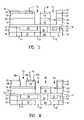
- FIGS. 1–11are cross-sectional, elevational views of the process steps employed to construct one embodiment of the air gap dielectric of the present invention in a semiconductor device.
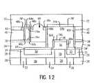
- FIG. 12is a cross-sectional, elevational view of an alternate embodiment of the final structure of the air gap dielectric of the present invention, wherein the lower cap layer is replaced by a self-aligned, selective metal deposition capping layer.
- FIG. 1depicts a dielectric stack deposited over a previously existing copper interconnect wiring level.
- the existing wiring levelhas a substrate dielectric layer 20 containing tungsten studs 22 , 24 , 26 , over which is deposited dielectric layer 28 containing copper wires 30 , 32 within TaN/Ta barrier layer 31 .
- dielectric layer 20may be phosphosilicate glass (PSG) while dielectric layer 28 may be undoped silicon glass (USG) or a glass containing silicon, carbon, oxygen and hydrogen (e.g., metholated SiO x , SiCOH).
- the dielectric stackconsists of, in order from the bottom, a cap layer 34 , e.g., silicon nitride Si 3 N 4 , an insulator layer with good mechanical properties and thermal conductivity 36 , e.g., USG or fluorinated silicon glass (FSG), an etch stop layer 38 , e.g.
- SiCSiC
- a layer of a dielectric (low k) material with good mechanical properties and thermal conductivity 40e.g., SiCOH
- a first hardmask layer 42e.g., silicon carbide SiC.
- Etch stop layer 38has a high etch rate ratio compared to underlying insulative layer 36
- insulative layer 40has a high etch rate ratio compared to etch stop layer 38 .
- An antireflective coating (ARC) layer 44 and resist layer 46are then applied and, as shown in FIG. 2 , are imaged for the trench pattern openings, and hardmask layer 42 is subsequently etched through the ARC and resist openings.
- ARCantireflective coating
- a second hardmask layer 48e.g., silicon dioxide SiO 2 or Si 3 N 4 , is deposited.
- a via resist layer 50is thereafter applied and imaged to create via resist pattern openings, as shown in FIG. 4 .
- the second hardmask layer 48 and the via openings 52 , 54are then etched through the pattern openings down to cap layer 34 , and via resist 50 is then stripped, as shown in FIG. 5 .
- FIG. 6depicts the blanket directional removal etch of second hardmask layer 48 , only above the upper surface of first hardmask layer 42 , which leaves second hardmask layer spacers 48 a, 48 b, 48 c adjacent to all areas of first hardmask layer 42 edges except areas exposed by via photo, i.e., no spacer is formed on the sidewalls of via 52 .
- spacers 48 a and 48 bare self-aligned and disposed adjacent trench/wire/via opening 56
- spacer 48 cis adjacent via opening 54 .
- the size of the spacersis determined by the thickness of each of the first and second hardmask layers.
- Trench 58joining via openings 52 and 54 , is then etched down to etch stop layer 38 .
- a conformal deposition of a second insulator layer 60e.g., SiO 2 or Si 3 N 4 , is applied over the exposed layers and into via openings 52 , 54 , and trenches 56 , 58 of the existing structure, as shown in FIG. 7 .
- Another etchis then performed for the blanket directional removal of portions of insulator layer 60 above hardmask layers 42 , 48 and etch stop layer 38 , and for the removal of the portions of insulator 60 at the bottom of via openings 52 , 54 , trench 56 , as well as the portions of cap layer 34 below via openings 52 and 54 .
- barrier-seed layer and copper deposition processesare used to fill the dual damascene structure, so that the trench and vias are first completely lined with a barrier (such as TaN/Ta) and seed layer 62 , and then filled with copper 64 , and then the excess material is removed by chemical mechanical polishing (CMP), as depicted in FIG. 9 .
- CMPchemical mechanical polishing
- other conductive materialssuch as aluminum, tungsten or gold may be employed.
- FIG. 10shows resist block mask 66 used to expose only those areas that will receive the air gap dielectric.
- the SiC, SiCOH, SiC exposed portions of layers 42 , 40 and 38are degraded by exposure to oxygen plasma, oxygen reactive ion etch (RIE) or oxygen implantation followed by a dilute HF etch which, as shown, creates a space 68 with an overhang 48 b, 48 c between unmasked minimum space lines 64 a, 64 b.
- RIEoxygen reactive ion etch
- supercritical CO 2provides the carrier medium for dilute HF to remove the oxygen-degraded films.
- insulative nitride cap layer 70e.g., silicon nitride or silicon carbon nitride
- silicon dioxide or FSG insulative layer 72are then applied, which close the air gap layer 68 , without completely filling it, as shown in FIG. 11 .
- air gap 68extends completely through cap layer 70 , and partially through insulative layer 72 , above the interconnect level. Extraneous fill of air gap 68 can be reduced by minimizing the opening between overhang 48 b and 48 c.
- a spin-on dielectric layerchosen because of its surface tension properties, may also be applied to leave air gap 68 unfilled.
- interconnect wire 64 afilling former trench opening 56
- interconnect wire 64 bfilling former trench 58 and via openings 52 , 54
- Spacers 60 b and 60 care formed along adjacent sides between wires 64 a, 64 b, and reduce the width of air gap 68 , so that the actual air gap dielectric width is less than the printed distance spacing wires 64 a, 64 b.
- the air gap dielectric 68 formed between interconnects 64 a, 64 balso extends above upper surfaces 74 a, 74 b of the wires and below lower surfaces 76 a, 76 b of the wires.
- Air gap 68 as formedis self-aligned to the adjacent sides of the interconnect wires 64 a, 64 b.
- FIG. 12Another embodiment, shown in completion in FIG. 12 , uses a similar process sequence as that described above, except that the silicon nitride Si 3 N 4 cap layers 34 and 70 are replaced by self-aligned metal capping layers 34 ′ and 70 ′ over copper wires 30 , 32 , 64 a, 64 b.
- Thismay be applied by a selective metal deposition process, and the metal capping layer may comprise either selective tungsten or a selective cobalt tungsten phosphide layer.
- insulative layer 72alone closes off the top of air gap 68 .
- the present inventionprovides a self aligned and adjustable air gap dielectric to reduce capacitance between adjacent, closely spaced conductive wires or vias.
- the height of the air gap above and below the adjacent copper linecan be selected to cut off fringing capacitance and increase the effective electrical resistance (k) of the structure.
- the preferred via dielectric employedis an oxide such as USG or FSG with relatively good mechanical properties and thermal conductivity.
- a sacrificial trench dielectric and etch stop layermay be used to create the air gap, and these may be made of higher thermal conductivity and mechanical strength materials.
- a block maskmay be used so that only areas on the chip with minimum spaces and a need for low capacitance receives the air gap. This maximizes the thermal conductance and mechanical stability of the chip.
- the trench and viaare defined by an oxide or nitride spacer, problems associated with liner/barrier precursors entering a porous, low-k dielectric are eliminated, as are issues of barrier integrity causing Cu contamination of the dielectric and issues of sidewall roughness causing Cu resistivity increase.
Landscapes
- Engineering & Computer Science (AREA)
- Physics & Mathematics (AREA)
- Condensed Matter Physics & Semiconductors (AREA)
- General Physics & Mathematics (AREA)
- Computer Hardware Design (AREA)
- Microelectronics & Electronic Packaging (AREA)
- Power Engineering (AREA)
- Manufacturing & Machinery (AREA)
- Internal Circuitry In Semiconductor Integrated Circuit Devices (AREA)
Abstract
Description
Claims (15)
Priority Applications (9)
| Application Number | Priority Date | Filing Date | Title |
|---|---|---|---|
| US10/605,440US7071532B2 (en) | 2003-09-30 | 2003-09-30 | Adjustable self-aligned air gap dielectric for low capacitance wiring |
| TW093128432ATWI319903B (en) | 2003-09-30 | 2004-09-20 | Adjustable self-aligned air gap dielectric for low capacitance wiring |
| KR1020067004177AKR100800360B1 (en) | 2003-09-30 | 2004-09-30 | Adjustable Self Aligning Air Gap Dielectric for Low Capacitance Wiring |
| EP04809842AEP1668692B1 (en) | 2003-09-30 | 2004-09-30 | Adjustable self-aligned air gap dielectric for low capacitance wiring |
| JP2006534155AJP5004585B2 (en) | 2003-09-30 | 2004-09-30 | Method for forming an air gap between a pair of interconnects on an interconnect layer in a semiconductor device |
| AT04809842TATE547809T1 (en) | 2003-09-30 | 2004-09-30 | DIELECTRIC WITH ADJUSTABLE SELF ALIGNED AIR GAP FOR LOW CAPACITY WIRING |
| PCT/US2004/032404WO2005034200A2 (en) | 2003-09-30 | 2004-09-30 | Adjustable self-aligned air gap dielectric for low capacitance wiring |
| CNB2004800274275ACN100466219C (en) | 2003-09-30 | 2004-09-30 | Adjustable Self-Aligning Air Gap Dielectric for Low Capacitance Routing |
| US11/418,921US7358148B2 (en) | 2003-09-30 | 2006-05-05 | Adjustable self-aligned air gap dielectric for low capacitance wiring |
Applications Claiming Priority (1)
| Application Number | Priority Date | Filing Date | Title |
|---|---|---|---|
| US10/605,440US7071532B2 (en) | 2003-09-30 | 2003-09-30 | Adjustable self-aligned air gap dielectric for low capacitance wiring |
Related Child Applications (1)
| Application Number | Title | Priority Date | Filing Date |
|---|---|---|---|
| US11/418,921DivisionUS7358148B2 (en) | 2003-09-30 | 2006-05-05 | Adjustable self-aligned air gap dielectric for low capacitance wiring |
Publications (2)
| Publication Number | Publication Date |
|---|---|
| US20050067673A1 US20050067673A1 (en) | 2005-03-31 |
| US7071532B2true US7071532B2 (en) | 2006-07-04 |
Family
ID=34375676
Family Applications (2)
| Application Number | Title | Priority Date | Filing Date |
|---|---|---|---|
| US10/605,440Expired - LifetimeUS7071532B2 (en) | 2003-09-30 | 2003-09-30 | Adjustable self-aligned air gap dielectric for low capacitance wiring |
| US11/418,921Expired - Fee RelatedUS7358148B2 (en) | 2003-09-30 | 2006-05-05 | Adjustable self-aligned air gap dielectric for low capacitance wiring |
Family Applications After (1)
| Application Number | Title | Priority Date | Filing Date |
|---|---|---|---|
| US11/418,921Expired - Fee RelatedUS7358148B2 (en) | 2003-09-30 | 2006-05-05 | Adjustable self-aligned air gap dielectric for low capacitance wiring |
Country Status (8)
| Country | Link |
|---|---|
| US (2) | US7071532B2 (en) |
| EP (1) | EP1668692B1 (en) |
| JP (1) | JP5004585B2 (en) |
| KR (1) | KR100800360B1 (en) |
| CN (1) | CN100466219C (en) |
| AT (1) | ATE547809T1 (en) |
| TW (1) | TWI319903B (en) |
| WO (1) | WO2005034200A2 (en) |
Cited By (161)
| Publication number | Priority date | Publication date | Assignee | Title |
|---|---|---|---|---|
| US20070075429A1 (en)* | 2003-12-11 | 2007-04-05 | Jae-Suk Lee | Metal interconnection lines of semiconductor devices and methods of forming the same |
| US20070182013A1 (en)* | 2005-12-31 | 2007-08-09 | Shanghai Ic R&D Center | Damascene structure having a reduced permittivity and manufacturing method thereof |
| US20090181537A1 (en)* | 2007-04-30 | 2009-07-16 | Advanced Micro Devices, Inc. | Semiconductor structure comprising an electrical connection and method of forming the same |
| US20100314767A1 (en)* | 2009-06-16 | 2010-12-16 | International Business Machines Corporation | Self-aligned dual damascene beol structures with patternable low- k material and methods of forming same |
| US20100319971A1 (en)* | 2009-06-17 | 2010-12-23 | International Business Machines Corporation | Airgap-containing interconnect structure with improved patternable low-k material and method of fabricating |
| US20110042790A1 (en)* | 2009-08-24 | 2011-02-24 | International Business Machines Corporation | MULTIPLE PATTERNING USING IMPROVED PATTERNABLE LOW-k DIELECTRIC MATERIALS |
| US20110049724A1 (en)* | 2009-08-26 | 2011-03-03 | International Business Machines Corporation | Beol interconnect structures and related fabrication methods |
| US20110074044A1 (en)* | 2009-09-29 | 2011-03-31 | International Business Machines Corporation | Patternable low-k dielectric interconnect structure with a graded cap layer and method of fabrication |
| US20110115090A1 (en)* | 2009-11-19 | 2011-05-19 | International Business Machines Corporation | Interconnect structure including a modified photoresist as a permanent interconnect dielectric and method of fabricating same |
| US20110115094A1 (en)* | 2009-11-16 | 2011-05-19 | International Business Machines Corporation | STRUCTURES AND METHODS FOR PHOTO-PATTERNABLE LOW-k (PPLK) INTEGRATION |
| US8241992B2 (en) | 2010-05-10 | 2012-08-14 | International Business Machines Corporation | Method for air gap interconnect integration using photo-patternable low k material |
| US8373271B2 (en) | 2010-05-27 | 2013-02-12 | International Business Machines Corporation | Interconnect structure with an oxygen-doped SiC antireflective coating and method of fabrication |
| US8497203B2 (en) | 2010-08-13 | 2013-07-30 | International Business Machines Corporation | Semiconductor structures and methods of manufacture |
| US20130221529A1 (en)* | 2007-01-22 | 2013-08-29 | International Business Machines Corporation | Hybrid interconnect structure for performance improvement and reliability enhancement |
| US8642252B2 (en) | 2010-03-10 | 2014-02-04 | International Business Machines Corporation | Methods for fabrication of an air gap-containing interconnect structure |
| US8822137B2 (en) | 2011-08-03 | 2014-09-02 | International Business Machines Corporation | Self-aligned fine pitch permanent on-chip interconnect structures and method of fabrication |
| US8890318B2 (en) | 2011-04-15 | 2014-11-18 | International Business Machines Corporation | Middle of line structures |
| US8896120B2 (en) | 2010-04-27 | 2014-11-25 | International Business Machines Corporation | Structures and methods for air gap integration |
| US8900988B2 (en) | 2011-04-15 | 2014-12-02 | International Business Machines Corporation | Method for forming self-aligned airgap interconnect structures |
| US8916936B2 (en) | 2012-08-22 | 2014-12-23 | Samsung Electronics Co., Ltd. | Transistor structure of a semiconductor device |
| US9054160B2 (en) | 2011-04-15 | 2015-06-09 | International Business Machines Corporation | Interconnect structure and method for fabricating on-chip interconnect structures by image reversal |
| US9159671B2 (en) | 2013-11-19 | 2015-10-13 | International Business Machines Corporation | Copper wire and dielectric with air gaps |
| US9159606B1 (en)* | 2014-07-31 | 2015-10-13 | Applied Materials, Inc. | Metal air gap |
| US9236298B2 (en) | 2011-09-08 | 2016-01-12 | Globalfoundries Inc. | Methods for fabrication interconnect structures with functional components and electrical conductive contact structures on a same level |
| US9269590B2 (en) | 2014-04-07 | 2016-02-23 | Applied Materials, Inc. | Spacer formation |
| US9287095B2 (en) | 2013-12-17 | 2016-03-15 | Applied Materials, Inc. | Semiconductor system assemblies and methods of operation |
| US9287134B2 (en) | 2014-01-17 | 2016-03-15 | Applied Materials, Inc. | Titanium oxide etch |
| US9293568B2 (en) | 2014-01-27 | 2016-03-22 | Applied Materials, Inc. | Method of fin patterning |
| US9299538B2 (en) | 2014-03-20 | 2016-03-29 | Applied Materials, Inc. | Radial waveguide systems and methods for post-match control of microwaves |
| US9299537B2 (en) | 2014-03-20 | 2016-03-29 | Applied Materials, Inc. | Radial waveguide systems and methods for post-match control of microwaves |
| US9299575B2 (en) | 2014-03-17 | 2016-03-29 | Applied Materials, Inc. | Gas-phase tungsten etch |
| US9299847B2 (en) | 2012-05-10 | 2016-03-29 | Globalfoundries Inc. | Printed transistor and fabrication method |
| US9299583B1 (en) | 2014-12-05 | 2016-03-29 | Applied Materials, Inc. | Aluminum oxide selective etch |
| US9309598B2 (en) | 2014-05-28 | 2016-04-12 | Applied Materials, Inc. | Oxide and metal removal |
| US9324576B2 (en) | 2010-05-27 | 2016-04-26 | Applied Materials, Inc. | Selective etch for silicon films |
| US9343272B1 (en) | 2015-01-08 | 2016-05-17 | Applied Materials, Inc. | Self-aligned process |
| US9349605B1 (en) | 2015-08-07 | 2016-05-24 | Applied Materials, Inc. | Oxide etch selectivity systems and methods |
| US9355856B2 (en) | 2014-09-12 | 2016-05-31 | Applied Materials, Inc. | V trench dry etch |
| US9355863B2 (en) | 2012-12-18 | 2016-05-31 | Applied Materials, Inc. | Non-local plasma oxide etch |
| US9355862B2 (en) | 2014-09-24 | 2016-05-31 | Applied Materials, Inc. | Fluorine-based hardmask removal |
| US9368364B2 (en) | 2014-09-24 | 2016-06-14 | Applied Materials, Inc. | Silicon etch process with tunable selectivity to SiO2 and other materials |
| US9373522B1 (en) | 2015-01-22 | 2016-06-21 | Applied Mateials, Inc. | Titanium nitride removal |
| US9373517B2 (en) | 2012-08-02 | 2016-06-21 | Applied Materials, Inc. | Semiconductor processing with DC assisted RF power for improved control |
| US9378969B2 (en) | 2014-06-19 | 2016-06-28 | Applied Materials, Inc. | Low temperature gas-phase carbon removal |
| US9378978B2 (en) | 2014-07-31 | 2016-06-28 | Applied Materials, Inc. | Integrated oxide recess and floating gate fin trimming |
| US9384997B2 (en) | 2012-11-20 | 2016-07-05 | Applied Materials, Inc. | Dry-etch selectivity |
| US9385028B2 (en) | 2014-02-03 | 2016-07-05 | Applied Materials, Inc. | Air gap process |
| US9390937B2 (en) | 2012-09-20 | 2016-07-12 | Applied Materials, Inc. | Silicon-carbon-nitride selective etch |
| US9396989B2 (en) | 2014-01-27 | 2016-07-19 | Applied Materials, Inc. | Air gaps between copper lines |
| US9406523B2 (en) | 2014-06-19 | 2016-08-02 | Applied Materials, Inc. | Highly selective doped oxide removal method |
| US9412608B2 (en) | 2012-11-30 | 2016-08-09 | Applied Materials, Inc. | Dry-etch for selective tungsten removal |
| US9418858B2 (en) | 2011-10-07 | 2016-08-16 | Applied Materials, Inc. | Selective etch of silicon by way of metastable hydrogen termination |
| US9425058B2 (en) | 2014-07-24 | 2016-08-23 | Applied Materials, Inc. | Simplified litho-etch-litho-etch process |
| US9425096B2 (en) | 2014-07-14 | 2016-08-23 | Qualcomm Incorporated | Air gap between tungsten metal lines for interconnects with reduced RC delay |
| US9431294B2 (en)* | 2014-10-28 | 2016-08-30 | GlobalFoundries, Inc. | Methods of producing integrated circuits with an air gap |
| US9437451B2 (en) | 2012-09-18 | 2016-09-06 | Applied Materials, Inc. | Radical-component oxide etch |
| US9449845B2 (en) | 2012-12-21 | 2016-09-20 | Applied Materials, Inc. | Selective titanium nitride etching |
| US9449850B2 (en) | 2013-03-15 | 2016-09-20 | Applied Materials, Inc. | Processing systems and methods for halide scavenging |
| US9449846B2 (en) | 2015-01-28 | 2016-09-20 | Applied Materials, Inc. | Vertical gate separation |
| US9472412B2 (en) | 2013-12-02 | 2016-10-18 | Applied Materials, Inc. | Procedure for etch rate consistency |
| US9472417B2 (en) | 2013-11-12 | 2016-10-18 | Applied Materials, Inc. | Plasma-free metal etch |
| US9478432B2 (en) | 2014-09-25 | 2016-10-25 | Applied Materials, Inc. | Silicon oxide selective removal |
| US9496167B2 (en) | 2014-07-31 | 2016-11-15 | Applied Materials, Inc. | Integrated bit-line airgap formation and gate stack post clean |
| US9493879B2 (en) | 2013-07-12 | 2016-11-15 | Applied Materials, Inc. | Selective sputtering for pattern transfer |
| US9499898B2 (en) | 2014-03-03 | 2016-11-22 | Applied Materials, Inc. | Layered thin film heater and method of fabrication |
| US9502258B2 (en) | 2014-12-23 | 2016-11-22 | Applied Materials, Inc. | Anisotropic gap etch |
| US9553102B2 (en) | 2014-08-19 | 2017-01-24 | Applied Materials, Inc. | Tungsten separation |
| US9576809B2 (en) | 2013-11-04 | 2017-02-21 | Applied Materials, Inc. | Etch suppression with germanium |
| US9607856B2 (en) | 2013-03-05 | 2017-03-28 | Applied Materials, Inc. | Selective titanium nitride removal |
| US9659753B2 (en) | 2014-08-07 | 2017-05-23 | Applied Materials, Inc. | Grooved insulator to reduce leakage current |
| US20170178949A1 (en)* | 2015-12-16 | 2017-06-22 | Samsung Electronics Co., Ltd. | Semiconductor devices |
| US9691645B2 (en) | 2015-08-06 | 2017-06-27 | Applied Materials, Inc. | Bolted wafer chuck thermal management systems and methods for wafer processing systems |
| US9721789B1 (en) | 2016-10-04 | 2017-08-01 | Applied Materials, Inc. | Saving ion-damaged spacers |
| US9728437B2 (en) | 2015-02-03 | 2017-08-08 | Applied Materials, Inc. | High temperature chuck for plasma processing systems |
| US9741593B2 (en) | 2015-08-06 | 2017-08-22 | Applied Materials, Inc. | Thermal management systems and methods for wafer processing systems |
| US9768034B1 (en) | 2016-11-11 | 2017-09-19 | Applied Materials, Inc. | Removal methods for high aspect ratio structures |
| US9773648B2 (en) | 2013-08-30 | 2017-09-26 | Applied Materials, Inc. | Dual discharge modes operation for remote plasma |
| US9786553B1 (en) | 2016-09-16 | 2017-10-10 | International Business Machines Corporation | Advanced BEOL interconnect structure containing uniform air gaps |
| US9842744B2 (en) | 2011-03-14 | 2017-12-12 | Applied Materials, Inc. | Methods for etch of SiN films |
| US9865484B1 (en) | 2016-06-29 | 2018-01-09 | Applied Materials, Inc. | Selective etch using material modification and RF pulsing |
| US9881805B2 (en) | 2015-03-02 | 2018-01-30 | Applied Materials, Inc. | Silicon selective removal |
| US9887096B2 (en) | 2012-09-17 | 2018-02-06 | Applied Materials, Inc. | Differential silicon oxide etch |
| US9885117B2 (en) | 2014-03-31 | 2018-02-06 | Applied Materials, Inc. | Conditioned semiconductor system parts |
| US9911652B1 (en) | 2017-03-29 | 2018-03-06 | International Business Machines Corporation | Forming self-aligned vias and air-gaps in semiconductor fabrication |
| US9934942B1 (en) | 2016-10-04 | 2018-04-03 | Applied Materials, Inc. | Chamber with flow-through source |
| US9947549B1 (en) | 2016-10-10 | 2018-04-17 | Applied Materials, Inc. | Cobalt-containing material removal |
| US9978564B2 (en) | 2012-09-21 | 2018-05-22 | Applied Materials, Inc. | Chemical control features in wafer process equipment |
| US10026621B2 (en) | 2016-11-14 | 2018-07-17 | Applied Materials, Inc. | SiN spacer profile patterning |
| US20180204760A1 (en)* | 2015-09-23 | 2018-07-19 | Intel Corporation | Maskless air gap to prevent via punch through |
| US10032711B2 (en) | 2016-07-25 | 2018-07-24 | International Business Machines Corporation | Integrating metal-insulator-metal capacitors with air gap process flow |
| US10043684B1 (en) | 2017-02-06 | 2018-08-07 | Applied Materials, Inc. | Self-limiting atomic thermal etching systems and methods |
| US10043674B1 (en) | 2017-08-04 | 2018-08-07 | Applied Materials, Inc. | Germanium etching systems and methods |
| US10049891B1 (en) | 2017-05-31 | 2018-08-14 | Applied Materials, Inc. | Selective in situ cobalt residue removal |
| US10062585B2 (en) | 2016-10-04 | 2018-08-28 | Applied Materials, Inc. | Oxygen compatible plasma source |
| US10062575B2 (en) | 2016-09-09 | 2018-08-28 | Applied Materials, Inc. | Poly directional etch by oxidation |
| US10062578B2 (en) | 2011-03-14 | 2018-08-28 | Applied Materials, Inc. | Methods for etch of metal and metal-oxide films |
| US10062587B2 (en) | 2012-07-18 | 2018-08-28 | Applied Materials, Inc. | Pedestal with multi-zone temperature control and multiple purge capabilities |
| US10062579B2 (en) | 2016-10-07 | 2018-08-28 | Applied Materials, Inc. | Selective SiN lateral recess |
| US10128086B1 (en) | 2017-10-24 | 2018-11-13 | Applied Materials, Inc. | Silicon pretreatment for nitride removal |
| US10163696B2 (en) | 2016-11-11 | 2018-12-25 | Applied Materials, Inc. | Selective cobalt removal for bottom up gapfill |
| US10170336B1 (en) | 2017-08-04 | 2019-01-01 | Applied Materials, Inc. | Methods for anisotropic control of selective silicon removal |
| US10224210B2 (en) | 2014-12-09 | 2019-03-05 | Applied Materials, Inc. | Plasma processing system with direct outlet toroidal plasma source |
| US10242908B2 (en) | 2016-11-14 | 2019-03-26 | Applied Materials, Inc. | Airgap formation with damage-free copper |
| US10256112B1 (en) | 2017-12-08 | 2019-04-09 | Applied Materials, Inc. | Selective tungsten removal |
| US10256079B2 (en) | 2013-02-08 | 2019-04-09 | Applied Materials, Inc. | Semiconductor processing systems having multiple plasma configurations |
| US10283321B2 (en) | 2011-01-18 | 2019-05-07 | Applied Materials, Inc. | Semiconductor processing system and methods using capacitively coupled plasma |
| US10283324B1 (en) | 2017-10-24 | 2019-05-07 | Applied Materials, Inc. | Oxygen treatment for nitride etching |
| US10297458B2 (en) | 2017-08-07 | 2019-05-21 | Applied Materials, Inc. | Process window widening using coated parts in plasma etch processes |
| US10319600B1 (en) | 2018-03-12 | 2019-06-11 | Applied Materials, Inc. | Thermal silicon etch |
| US10319739B2 (en) | 2017-02-08 | 2019-06-11 | Applied Materials, Inc. | Accommodating imperfectly aligned memory holes |
| US10319649B2 (en) | 2017-04-11 | 2019-06-11 | Applied Materials, Inc. | Optical emission spectroscopy (OES) for remote plasma monitoring |
| US10354889B2 (en) | 2017-07-17 | 2019-07-16 | Applied Materials, Inc. | Non-halogen etching of silicon-containing materials |
| US10403507B2 (en) | 2017-02-03 | 2019-09-03 | Applied Materials, Inc. | Shaped etch profile with oxidation |
| US10424485B2 (en) | 2013-03-01 | 2019-09-24 | Applied Materials, Inc. | Enhanced etching processes using remote plasma sources |
| US10431429B2 (en) | 2017-02-03 | 2019-10-01 | Applied Materials, Inc. | Systems and methods for radial and azimuthal control of plasma uniformity |
| US10468267B2 (en) | 2017-05-31 | 2019-11-05 | Applied Materials, Inc. | Water-free etching methods |
| US10490418B2 (en) | 2014-10-14 | 2019-11-26 | Applied Materials, Inc. | Systems and methods for internal surface conditioning assessment in plasma processing equipment |
| US10490406B2 (en) | 2018-04-10 | 2019-11-26 | Appled Materials, Inc. | Systems and methods for material breakthrough |
| US10497573B2 (en) | 2018-03-13 | 2019-12-03 | Applied Materials, Inc. | Selective atomic layer etching of semiconductor materials |
| US10504700B2 (en) | 2015-08-27 | 2019-12-10 | Applied Materials, Inc. | Plasma etching systems and methods with secondary plasma injection |
| US10504754B2 (en) | 2016-05-19 | 2019-12-10 | Applied Materials, Inc. | Systems and methods for improved semiconductor etching and component protection |
| US10522371B2 (en) | 2016-05-19 | 2019-12-31 | Applied Materials, Inc. | Systems and methods for improved semiconductor etching and component protection |
| US10541184B2 (en) | 2017-07-11 | 2020-01-21 | Applied Materials, Inc. | Optical emission spectroscopic techniques for monitoring etching |
| US10541246B2 (en) | 2017-06-26 | 2020-01-21 | Applied Materials, Inc. | 3D flash memory cells which discourage cross-cell electrical tunneling |
| US10546729B2 (en) | 2016-10-04 | 2020-01-28 | Applied Materials, Inc. | Dual-channel showerhead with improved profile |
| US10566206B2 (en) | 2016-12-27 | 2020-02-18 | Applied Materials, Inc. | Systems and methods for anisotropic material breakthrough |
| US10573496B2 (en) | 2014-12-09 | 2020-02-25 | Applied Materials, Inc. | Direct outlet toroidal plasma source |
| US10573527B2 (en) | 2018-04-06 | 2020-02-25 | Applied Materials, Inc. | Gas-phase selective etching systems and methods |
| US10593560B2 (en) | 2018-03-01 | 2020-03-17 | Applied Materials, Inc. | Magnetic induction plasma source for semiconductor processes and equipment |
| US10593523B2 (en) | 2014-10-14 | 2020-03-17 | Applied Materials, Inc. | Systems and methods for internal surface conditioning in plasma processing equipment |
| US10615047B2 (en) | 2018-02-28 | 2020-04-07 | Applied Materials, Inc. | Systems and methods to form airgaps |
| US10629473B2 (en) | 2016-09-09 | 2020-04-21 | Applied Materials, Inc. | Footing removal for nitride spacer |
| US10672642B2 (en) | 2018-07-24 | 2020-06-02 | Applied Materials, Inc. | Systems and methods for pedestal configuration |
| US10679870B2 (en) | 2018-02-15 | 2020-06-09 | Applied Materials, Inc. | Semiconductor processing chamber multistage mixing apparatus |
| US10699879B2 (en) | 2018-04-17 | 2020-06-30 | Applied Materials, Inc. | Two piece electrode assembly with gap for plasma control |
| US10727080B2 (en) | 2017-07-07 | 2020-07-28 | Applied Materials, Inc. | Tantalum-containing material removal |
| US10755941B2 (en) | 2018-07-06 | 2020-08-25 | Applied Materials, Inc. | Self-limiting selective etching systems and methods |
| US10854426B2 (en) | 2018-01-08 | 2020-12-01 | Applied Materials, Inc. | Metal recess for semiconductor structures |
| US10872778B2 (en) | 2018-07-06 | 2020-12-22 | Applied Materials, Inc. | Systems and methods utilizing solid-phase etchants |
| US10886137B2 (en) | 2018-04-30 | 2021-01-05 | Applied Materials, Inc. | Selective nitride removal |
| US10892198B2 (en) | 2018-09-14 | 2021-01-12 | Applied Materials, Inc. | Systems and methods for improved performance in semiconductor processing |
| US10903054B2 (en) | 2017-12-19 | 2021-01-26 | Applied Materials, Inc. | Multi-zone gas distribution systems and methods |
| US10920319B2 (en) | 2019-01-11 | 2021-02-16 | Applied Materials, Inc. | Ceramic showerheads with conductive electrodes |
| US10920320B2 (en) | 2017-06-16 | 2021-02-16 | Applied Materials, Inc. | Plasma health determination in semiconductor substrate processing reactors |
| US10943834B2 (en) | 2017-03-13 | 2021-03-09 | Applied Materials, Inc. | Replacement contact process |
| US10964512B2 (en) | 2018-02-15 | 2021-03-30 | Applied Materials, Inc. | Semiconductor processing chamber multistage mixing apparatus and methods |
| US11049755B2 (en) | 2018-09-14 | 2021-06-29 | Applied Materials, Inc. | Semiconductor substrate supports with embedded RF shield |
| US11062887B2 (en) | 2018-09-17 | 2021-07-13 | Applied Materials, Inc. | High temperature RF heater pedestals |
| US11121002B2 (en) | 2018-10-24 | 2021-09-14 | Applied Materials, Inc. | Systems and methods for etching metals and metal derivatives |
| US11239061B2 (en) | 2014-11-26 | 2022-02-01 | Applied Materials, Inc. | Methods and systems to enhance process uniformity |
| US11257693B2 (en) | 2015-01-09 | 2022-02-22 | Applied Materials, Inc. | Methods and systems to improve pedestal temperature control |
| US11276590B2 (en) | 2017-05-17 | 2022-03-15 | Applied Materials, Inc. | Multi-zone semiconductor substrate supports |
| US11276559B2 (en) | 2017-05-17 | 2022-03-15 | Applied Materials, Inc. | Semiconductor processing chamber for multiple precursor flow |
| US11289371B2 (en) | 2020-01-23 | 2022-03-29 | International Business Machines Corporation | Top vias with selectively retained etch stops |
| US11328909B2 (en) | 2017-12-22 | 2022-05-10 | Applied Materials, Inc. | Chamber conditioning and removal processes |
| US11417534B2 (en) | 2018-09-21 | 2022-08-16 | Applied Materials, Inc. | Selective material removal |
| US11437242B2 (en) | 2018-11-27 | 2022-09-06 | Applied Materials, Inc. | Selective removal of silicon-containing materials |
| US11594428B2 (en) | 2015-02-03 | 2023-02-28 | Applied Materials, Inc. | Low temperature chuck for plasma processing systems |
| US11682560B2 (en) | 2018-10-11 | 2023-06-20 | Applied Materials, Inc. | Systems and methods for hafnium-containing film removal |
| US11721527B2 (en) | 2019-01-07 | 2023-08-08 | Applied Materials, Inc. | Processing chamber mixing systems |
| US12340979B2 (en) | 2017-05-17 | 2025-06-24 | Applied Materials, Inc. | Semiconductor processing chamber for improved precursor flow |
Families Citing this family (33)
| Publication number | Priority date | Publication date | Assignee | Title |
|---|---|---|---|---|
| DE102004003337A1 (en)* | 2004-01-22 | 2005-08-18 | Infineon Technologies Ag | Plasma enhanced chemical vapor deposition method, silicon-oxygen-nitrogen containing material and layer assembly |
| KR20050114784A (en)* | 2004-06-01 | 2005-12-07 | 동부아남반도체 주식회사 | Method for forming cu interconnection of semiconductor device |
| DE102004050391B4 (en)* | 2004-10-15 | 2007-02-08 | Infineon Technologies Ag | Method for producing a layer arrangement and layer arrangement |
| KR100632653B1 (en)* | 2005-04-22 | 2006-10-12 | 주식회사 하이닉스반도체 | Bit line formation method of semiconductor device |
| US7629225B2 (en)* | 2005-06-13 | 2009-12-08 | Infineon Technologies Ag | Methods of manufacturing semiconductor devices and structures thereof |
| EP1744359A1 (en)* | 2005-07-12 | 2007-01-17 | ST Microelectronics Crolles 2 SAS | Interconnect structure having cavities in its dielectric portion |
| KR100672731B1 (en)* | 2005-10-04 | 2007-01-24 | 동부일렉트로닉스 주식회사 | Metal wiring formation method of semiconductor device |
| EP2005468A1 (en) | 2006-03-30 | 2008-12-24 | Koninklijke Philips Electronics N.V. | Improving control of localized air gap formation in an interconnect stack |
| US7951723B2 (en)* | 2006-10-24 | 2011-05-31 | Taiwan Semiconductor Manufacturing Company, Ltd. | Integrated etch and supercritical CO2 process and chamber design |
| WO2008056295A1 (en)* | 2006-11-09 | 2008-05-15 | Nxp B.V. | A semiconductor device and a method of manufacturing thereof |
| US20080185722A1 (en)* | 2007-02-05 | 2008-08-07 | Chung-Shi Liu | Formation process of interconnect structures with air-gaps and sidewall spacers |
| KR100854860B1 (en)* | 2007-06-27 | 2008-08-28 | 주식회사 하이닉스반도체 | Manufacturing Method of Memory Device |
| US20090072409A1 (en)* | 2007-09-14 | 2009-03-19 | International Business Machines Corporation | Interconnect Structures Incorporating Air-Gap Spacers |
| US20090075470A1 (en)* | 2007-09-14 | 2009-03-19 | International Business Machines Corporation | Method for Manufacturing Interconnect Structures Incorporating Air-Gap Spacers |
| US8476758B2 (en)* | 2008-01-09 | 2013-07-02 | International Business Machines Corporation | Airgap-containing interconnect structure with patternable low-k material and method of fabricating |
| US8108820B2 (en)* | 2008-09-11 | 2012-01-31 | International Business Machines Corporation | Enhanced conductivity in an airgapped integrated circuit |
| JP5491077B2 (en)* | 2009-06-08 | 2014-05-14 | キヤノン株式会社 | Semiconductor device and manufacturing method of semiconductor device |
| US7790601B1 (en)* | 2009-09-17 | 2010-09-07 | International Business Machines Corporation | Forming interconnects with air gaps |
| US8357609B2 (en)* | 2010-05-04 | 2013-01-22 | Globalfoundries Inc. | Dual damascene-like subtractive metal etch scheme |
| CN103137545B (en)* | 2011-11-25 | 2015-08-05 | 中芯国际集成电路制造(上海)有限公司 | Semiconductor device and forming method thereof |
| CN103165519B (en)* | 2011-12-08 | 2016-07-27 | 中芯国际集成电路制造(上海)有限公司 | A kind of manufacture method of semiconductor device |
| CN103178000B (en)* | 2011-12-20 | 2014-11-05 | 中芯国际集成电路制造(上海)有限公司 | Semiconductor device and forming method thereof |
| US8847401B2 (en) | 2012-10-31 | 2014-09-30 | International Business Machines Corporation | Semiconductor structure incorporating a contact sidewall spacer with a self-aligned airgap and a method of forming the semiconductor structure |
| KR102334736B1 (en)* | 2015-12-03 | 2021-12-03 | 삼성전자주식회사 | Semiconductor device and method for manufacturing the semiconductor device |
| US9905463B2 (en) | 2015-12-15 | 2018-02-27 | International Business Machines Corporation | Self-aligned low dielectric constant gate cap and a method of forming the same |
| US9349687B1 (en) | 2015-12-19 | 2016-05-24 | International Business Machines Corporation | Advanced manganese/manganese nitride cap/etch mask for air gap formation scheme in nanocopper low-K interconnect |
| US9859212B1 (en) | 2016-07-12 | 2018-01-02 | International Business Machines Corporation | Multi-level air gap formation in dual-damascene structure |
| US10629478B2 (en)* | 2017-08-22 | 2020-04-21 | International Business Machines Corporation | Dual-damascene formation with dielectric spacer and thin liner |
| US10319629B1 (en)* | 2018-05-08 | 2019-06-11 | International Business Machines Corporation | Skip via for metal interconnects |
| US11469189B2 (en)* | 2018-06-29 | 2022-10-11 | Intel Corporation | Inductor and transmission line with air gap |
| CN112885773B (en)* | 2019-11-29 | 2024-10-22 | 长鑫存储技术有限公司 | Semiconductor structure and manufacturing method thereof |
| US20210265205A1 (en)* | 2020-02-25 | 2021-08-26 | Tokyo Electron Limited | Dielectric etch stop layer for reactive ion etch (rie) lag reduction and chamfer corner protection |
| CN111501025B (en)* | 2020-04-23 | 2022-05-27 | 北京北方华创微电子装备有限公司 | Deposition apparatus |
Citations (14)
| Publication number | Priority date | Publication date | Assignee | Title |
|---|---|---|---|---|
| US5117276A (en)* | 1989-08-14 | 1992-05-26 | Fairchild Camera And Instrument Corp. | High performance interconnect system for an integrated circuit |
| US5324683A (en) | 1993-06-02 | 1994-06-28 | Motorola, Inc. | Method of forming a semiconductor structure having an air region |
| US6150232A (en) | 1999-02-05 | 2000-11-21 | Chartered Semiconductor Manufacturing Ltd. | Formation of low k dielectric |
| US6200900B1 (en) | 1999-10-08 | 2001-03-13 | National Semiconductor Corporation | Method for formation of an air gap in an integrated circuit architecture |
| US6211057B1 (en)* | 1999-09-03 | 2001-04-03 | Taiwan Semiconductor Manufacturing Company | Method for manufacturing arch air gap in multilevel interconnection |
| US6281585B1 (en) | 1997-06-30 | 2001-08-28 | Philips Electronics North America Corporation | Air gap dielectric in self-aligned via structures |
| US20010023123A1 (en) | 1999-12-24 | 2001-09-20 | Kim Jin-Woong | Method for forming semiconductor device having low parasite capacitance using air gap and self-aligned contact plug |
| US6329279B1 (en) | 2000-03-20 | 2001-12-11 | United Microelectronics Corp. | Method of fabricating metal interconnect structure having outer air spacer |
| US6413852B1 (en)* | 2000-08-31 | 2002-07-02 | International Business Machines Corporation | Method of forming multilevel interconnect structure containing air gaps including utilizing both sacrificial and placeholder material |
| US6423629B1 (en) | 2000-05-31 | 2002-07-23 | Kie Y. Ahn | Multilevel copper interconnects with low-k dielectrics and air gaps |
| US6472266B1 (en) | 2001-06-18 | 2002-10-29 | Taiwan Semiconductor Manufacturing Company | Method to reduce bit line capacitance in cub drams |
| US6545361B2 (en)* | 1997-11-06 | 2003-04-08 | Matsushita Electric Industrial Co., Ltd. | Semiconductor device having multilevel interconnection structure and method for fabricating the same |
| US20040097065A1 (en)* | 2002-11-15 | 2004-05-20 | Water Lur | Air gap for tungsten/aluminum plug applications |
| US6838354B2 (en)* | 2002-12-20 | 2005-01-04 | Freescale Semiconductor, Inc. | Method for forming a passivation layer for air gap formation |
Family Cites Families (10)
| Publication number | Priority date | Publication date | Assignee | Title |
|---|---|---|---|---|
| JPH0722583A (en)* | 1992-12-15 | 1995-01-24 | Internatl Business Mach Corp <Ibm> | Multilayer circuit device |
| US6184121B1 (en)* | 1997-07-10 | 2001-02-06 | International Business Machines Corporation | Chip interconnect wiring structure with low dielectric constant insulator and methods for fabricating the same |
| JP2971454B2 (en)* | 1997-08-21 | 1999-11-08 | 松下電子工業株式会社 | Semiconductor device and manufacturing method thereof |
| US6333255B1 (en)* | 1997-08-21 | 2001-12-25 | Matsushita Electronics Corporation | Method for making semiconductor device containing low carbon film for interconnect structures |
| FR2784230B1 (en) | 1998-10-05 | 2000-12-29 | St Microelectronics Sa | METHOD FOR PRODUCING INTER AND / OR INTRA-METALLIC AIR INSULATION IN AN INTEGRATED CIRCUIT AND INTEGRATED INTEGRATED CIRCUIT |
| US6211561B1 (en)* | 1998-11-16 | 2001-04-03 | Conexant Systems, Inc. | Interconnect structure and method employing air gaps between metal lines and between metal layers |
| US6177329B1 (en)* | 1999-04-15 | 2001-01-23 | Kurt Pang | Integrated circuit structures having gas pockets and method for forming integrated circuit structures having gas pockets |
| JP5156155B2 (en)* | 1999-10-13 | 2013-03-06 | アプライド マテリアルズ インコーポレイテッド | Method for manufacturing a semiconductor integrated circuit |
| US6815329B2 (en)* | 2000-02-08 | 2004-11-09 | International Business Machines Corporation | Multilayer interconnect structure containing air gaps and method for making |
| DE10140754A1 (en) | 2001-08-20 | 2003-03-27 | Infineon Technologies Ag | Circuit arrangement and method for manufacturing a circuit arrangement |
- 2003
- 2003-09-30USUS10/605,440patent/US7071532B2/ennot_activeExpired - Lifetime
- 2004
- 2004-09-20TWTW093128432Apatent/TWI319903B/ennot_activeIP Right Cessation
- 2004-09-30ATAT04809842Tpatent/ATE547809T1/enactive
- 2004-09-30KRKR1020067004177Apatent/KR100800360B1/ennot_activeExpired - Fee Related
- 2004-09-30WOPCT/US2004/032404patent/WO2005034200A2/enactiveApplication Filing
- 2004-09-30CNCNB2004800274275Apatent/CN100466219C/ennot_activeExpired - Fee Related
- 2004-09-30EPEP04809842Apatent/EP1668692B1/ennot_activeExpired - Lifetime
- 2004-09-30JPJP2006534155Apatent/JP5004585B2/ennot_activeExpired - Fee Related
- 2006
- 2006-05-05USUS11/418,921patent/US7358148B2/ennot_activeExpired - Fee Related
Patent Citations (16)
| Publication number | Priority date | Publication date | Assignee | Title |
|---|---|---|---|---|
| US5117276A (en)* | 1989-08-14 | 1992-05-26 | Fairchild Camera And Instrument Corp. | High performance interconnect system for an integrated circuit |
| US5324683A (en) | 1993-06-02 | 1994-06-28 | Motorola, Inc. | Method of forming a semiconductor structure having an air region |
| US5510645A (en)* | 1993-06-02 | 1996-04-23 | Motorola, Inc. | Semiconductor structure having an air region and method of forming the semiconductor structure |
| US6281585B1 (en) | 1997-06-30 | 2001-08-28 | Philips Electronics North America Corporation | Air gap dielectric in self-aligned via structures |
| US6545361B2 (en)* | 1997-11-06 | 2003-04-08 | Matsushita Electric Industrial Co., Ltd. | Semiconductor device having multilevel interconnection structure and method for fabricating the same |
| US6150232A (en) | 1999-02-05 | 2000-11-21 | Chartered Semiconductor Manufacturing Ltd. | Formation of low k dielectric |
| US6211057B1 (en)* | 1999-09-03 | 2001-04-03 | Taiwan Semiconductor Manufacturing Company | Method for manufacturing arch air gap in multilevel interconnection |
| US6200900B1 (en) | 1999-10-08 | 2001-03-13 | National Semiconductor Corporation | Method for formation of an air gap in an integrated circuit architecture |
| US20010023123A1 (en) | 1999-12-24 | 2001-09-20 | Kim Jin-Woong | Method for forming semiconductor device having low parasite capacitance using air gap and self-aligned contact plug |
| US6329279B1 (en) | 2000-03-20 | 2001-12-11 | United Microelectronics Corp. | Method of fabricating metal interconnect structure having outer air spacer |
| US6423629B1 (en) | 2000-05-31 | 2002-07-23 | Kie Y. Ahn | Multilevel copper interconnects with low-k dielectrics and air gaps |
| US20020127844A1 (en) | 2000-08-31 | 2002-09-12 | International Business Machines Corporation | Multilevel interconnect structure containing air gaps and method for making |
| US6413852B1 (en)* | 2000-08-31 | 2002-07-02 | International Business Machines Corporation | Method of forming multilevel interconnect structure containing air gaps including utilizing both sacrificial and placeholder material |
| US6472266B1 (en) | 2001-06-18 | 2002-10-29 | Taiwan Semiconductor Manufacturing Company | Method to reduce bit line capacitance in cub drams |
| US20040097065A1 (en)* | 2002-11-15 | 2004-05-20 | Water Lur | Air gap for tungsten/aluminum plug applications |
| US6838354B2 (en)* | 2002-12-20 | 2005-01-04 | Freescale Semiconductor, Inc. | Method for forming a passivation layer for air gap formation |
Non-Patent Citations (1)
| Title |
|---|
| V. Arnal, J. Torres, P. Gayet, R. Gonella, P. Spinelli, M. Guillermet, J-P Reynard, GC. Verove; "Integration of a 3 Level CuSiO2 Air Gap Interconnect for Sub 0.1 micron DMOS Technologies;" IEEE, Jun. 2001, pp. 298-300. |
Cited By (243)
| Publication number | Priority date | Publication date | Assignee | Title |
|---|---|---|---|---|
| US7514793B2 (en)* | 2003-12-11 | 2009-04-07 | Dongbu Electronics Co., Ltd. | Metal interconnection lines of semiconductor devices and methods of forming the same |
| US20070075429A1 (en)* | 2003-12-11 | 2007-04-05 | Jae-Suk Lee | Metal interconnection lines of semiconductor devices and methods of forming the same |
| US7602038B2 (en)* | 2005-12-31 | 2009-10-13 | Shanghai Ic R&D Center | Damascene structure having a reduced permittivity and manufacturing method thereof |
| US20070182013A1 (en)* | 2005-12-31 | 2007-08-09 | Shanghai Ic R&D Center | Damascene structure having a reduced permittivity and manufacturing method thereof |
| US20130230983A1 (en)* | 2007-01-22 | 2013-09-05 | International Business Machines Corporation | Hybrid interconnect structure for performance improvement and reliability enhancement |
| US8753979B2 (en)* | 2007-01-22 | 2014-06-17 | International Business Machines Corporation | Hybrid interconnect structure for performance improvement and reliability enhancement |
| US20130221529A1 (en)* | 2007-01-22 | 2013-08-29 | International Business Machines Corporation | Hybrid interconnect structure for performance improvement and reliability enhancement |
| US8754526B2 (en)* | 2007-01-22 | 2014-06-17 | International Business Machines Corporation | Hybrid interconnect structure for performance improvement and reliability enhancement |
| US20130228925A1 (en)* | 2007-01-22 | 2013-09-05 | International Business Machines Corporation | Hybrid interconnect structure for performance improvement and reliability enhancement |
| US8796854B2 (en)* | 2007-01-22 | 2014-08-05 | International Business Machines Corporation | Hybrid interconnect structure for performance improvement and reliability enhancement |
| US20090181537A1 (en)* | 2007-04-30 | 2009-07-16 | Advanced Micro Devices, Inc. | Semiconductor structure comprising an electrical connection and method of forming the same |
| US20100314767A1 (en)* | 2009-06-16 | 2010-12-16 | International Business Machines Corporation | Self-aligned dual damascene beol structures with patternable low- k material and methods of forming same |
| US8519540B2 (en) | 2009-06-16 | 2013-08-27 | International Business Machines Corporation | Self-aligned dual damascene BEOL structures with patternable low- K material and methods of forming same |
| US8415248B2 (en) | 2009-06-16 | 2013-04-09 | International Business Machines Corporation | Self-aligned dual damascene BEOL structures with patternable low-k material and methods of forming same |
| US8659115B2 (en) | 2009-06-17 | 2014-02-25 | International Business Machines Corporation | Airgap-containing interconnect structure with improved patternable low-K material and method of fabricating |
| US20100319971A1 (en)* | 2009-06-17 | 2010-12-23 | International Business Machines Corporation | Airgap-containing interconnect structure with improved patternable low-k material and method of fabricating |
| US8487411B2 (en) | 2009-08-24 | 2013-07-16 | International Business Machines Corporation | Multiple patterning using improved patternable low-κ dielectric materials |
| US20110042790A1 (en)* | 2009-08-24 | 2011-02-24 | International Business Machines Corporation | MULTIPLE PATTERNING USING IMPROVED PATTERNABLE LOW-k DIELECTRIC MATERIALS |
| US8163658B2 (en) | 2009-08-24 | 2012-04-24 | International Business Machines Corporation | Multiple patterning using improved patternable low-k dielectric materials |
| US8003516B2 (en) | 2009-08-26 | 2011-08-23 | International Business Machines Corporation | BEOL interconnect structures and related fabrication methods |
| US20110049724A1 (en)* | 2009-08-26 | 2011-03-03 | International Business Machines Corporation | Beol interconnect structures and related fabrication methods |
| US8461039B2 (en) | 2009-09-29 | 2013-06-11 | International Business Machines Corporation | Patternable low-K dielectric interconnect structure with a graded cap layer and method of fabrication |
| US20110074044A1 (en)* | 2009-09-29 | 2011-03-31 | International Business Machines Corporation | Patternable low-k dielectric interconnect structure with a graded cap layer and method of fabrication |
| US8202783B2 (en) | 2009-09-29 | 2012-06-19 | International Business Machines Corporation | Patternable low-k dielectric interconnect structure with a graded cap layer and method of fabrication |
| US8637395B2 (en) | 2009-11-16 | 2014-01-28 | International Business Machines Corporation | Methods for photo-patternable low-k (PPLK) integration with curing after pattern transfer |
| US9059249B2 (en) | 2009-11-16 | 2015-06-16 | International Business Machines Corporation | Interconnect structures containing a photo-patternable low-k dielectric with a curved sidewall surface |
| US20110115094A1 (en)* | 2009-11-16 | 2011-05-19 | International Business Machines Corporation | STRUCTURES AND METHODS FOR PHOTO-PATTERNABLE LOW-k (PPLK) INTEGRATION |
| US9431295B2 (en) | 2009-11-19 | 2016-08-30 | Globalfoundries Inc. | Interconnect structure including a modified photoresist as a permanent interconnect dielectric and method of fabricating same |
| US20110115090A1 (en)* | 2009-11-19 | 2011-05-19 | International Business Machines Corporation | Interconnect structure including a modified photoresist as a permanent interconnect dielectric and method of fabricating same |
| US8367540B2 (en) | 2009-11-19 | 2013-02-05 | International Business Machines Corporation | Interconnect structure including a modified photoresist as a permanent interconnect dielectric and method of fabricating same |
| US8952539B2 (en) | 2010-03-10 | 2015-02-10 | International Business Machines Corporation | Methods for fabrication of an air gap-containing interconnect structure |
| US8642252B2 (en) | 2010-03-10 | 2014-02-04 | International Business Machines Corporation | Methods for fabrication of an air gap-containing interconnect structure |
| US8896120B2 (en) | 2010-04-27 | 2014-11-25 | International Business Machines Corporation | Structures and methods for air gap integration |
| US8241992B2 (en) | 2010-05-10 | 2012-08-14 | International Business Machines Corporation | Method for air gap interconnect integration using photo-patternable low k material |
| US8629561B2 (en) | 2010-05-10 | 2014-01-14 | International Business Machines Corporation | Air gap-containing interconnect structure having photo-patternable low k material |
| US9324576B2 (en) | 2010-05-27 | 2016-04-26 | Applied Materials, Inc. | Selective etch for silicon films |
| US8373271B2 (en) | 2010-05-27 | 2013-02-12 | International Business Machines Corporation | Interconnect structure with an oxygen-doped SiC antireflective coating and method of fabrication |
| US9754800B2 (en) | 2010-05-27 | 2017-09-05 | Applied Materials, Inc. | Selective etch for silicon films |
| US8497203B2 (en) | 2010-08-13 | 2013-07-30 | International Business Machines Corporation | Semiconductor structures and methods of manufacture |
| US10283321B2 (en) | 2011-01-18 | 2019-05-07 | Applied Materials, Inc. | Semiconductor processing system and methods using capacitively coupled plasma |
| US10062578B2 (en) | 2011-03-14 | 2018-08-28 | Applied Materials, Inc. | Methods for etch of metal and metal-oxide films |
| US9842744B2 (en) | 2011-03-14 | 2017-12-12 | Applied Materials, Inc. | Methods for etch of SiN films |
| US8900988B2 (en) | 2011-04-15 | 2014-12-02 | International Business Machines Corporation | Method for forming self-aligned airgap interconnect structures |
| US9490202B2 (en) | 2011-04-15 | 2016-11-08 | GlobalFoundries, Inc. | Self-aligned airgap interconnect structures |
| US9054160B2 (en) | 2011-04-15 | 2015-06-09 | International Business Machines Corporation | Interconnect structure and method for fabricating on-chip interconnect structures by image reversal |
| US8890318B2 (en) | 2011-04-15 | 2014-11-18 | International Business Machines Corporation | Middle of line structures |
| US9245791B2 (en) | 2011-04-15 | 2016-01-26 | Globalfoundries Inc. | Method for fabricating a contact |
| US9343354B2 (en) | 2011-04-15 | 2016-05-17 | Globalfoundries Inc. | Middle of line structures and methods for fabrication |
| US8822137B2 (en) | 2011-08-03 | 2014-09-02 | International Business Machines Corporation | Self-aligned fine pitch permanent on-chip interconnect structures and method of fabrication |
| US9209126B2 (en) | 2011-08-03 | 2015-12-08 | Globalfoundries Inc. | Self-aligned fine pitch permanent on-chip interconnect structures and method of fabrication |
| US9236298B2 (en) | 2011-09-08 | 2016-01-12 | Globalfoundries Inc. | Methods for fabrication interconnect structures with functional components and electrical conductive contact structures on a same level |
| US9418858B2 (en) | 2011-10-07 | 2016-08-16 | Applied Materials, Inc. | Selective etch of silicon by way of metastable hydrogen termination |
| US9299847B2 (en) | 2012-05-10 | 2016-03-29 | Globalfoundries Inc. | Printed transistor and fabrication method |
| US10062587B2 (en) | 2012-07-18 | 2018-08-28 | Applied Materials, Inc. | Pedestal with multi-zone temperature control and multiple purge capabilities |
| US10032606B2 (en) | 2012-08-02 | 2018-07-24 | Applied Materials, Inc. | Semiconductor processing with DC assisted RF power for improved control |
| US9373517B2 (en) | 2012-08-02 | 2016-06-21 | Applied Materials, Inc. | Semiconductor processing with DC assisted RF power for improved control |
| US8916936B2 (en) | 2012-08-22 | 2014-12-23 | Samsung Electronics Co., Ltd. | Transistor structure of a semiconductor device |
| US9305921B2 (en) | 2012-08-22 | 2016-04-05 | Samsung Electronics Co., Ltd. | Semiconductor device |
| US9887096B2 (en) | 2012-09-17 | 2018-02-06 | Applied Materials, Inc. | Differential silicon oxide etch |
| US9437451B2 (en) | 2012-09-18 | 2016-09-06 | Applied Materials, Inc. | Radical-component oxide etch |
| US9390937B2 (en) | 2012-09-20 | 2016-07-12 | Applied Materials, Inc. | Silicon-carbon-nitride selective etch |
| US10354843B2 (en) | 2012-09-21 | 2019-07-16 | Applied Materials, Inc. | Chemical control features in wafer process equipment |
| US11264213B2 (en) | 2012-09-21 | 2022-03-01 | Applied Materials, Inc. | Chemical control features in wafer process equipment |
| US9978564B2 (en) | 2012-09-21 | 2018-05-22 | Applied Materials, Inc. | Chemical control features in wafer process equipment |
| US9384997B2 (en) | 2012-11-20 | 2016-07-05 | Applied Materials, Inc. | Dry-etch selectivity |
| US9412608B2 (en) | 2012-11-30 | 2016-08-09 | Applied Materials, Inc. | Dry-etch for selective tungsten removal |
| US9355863B2 (en) | 2012-12-18 | 2016-05-31 | Applied Materials, Inc. | Non-local plasma oxide etch |
| US9449845B2 (en) | 2012-12-21 | 2016-09-20 | Applied Materials, Inc. | Selective titanium nitride etching |
| US11024486B2 (en) | 2013-02-08 | 2021-06-01 | Applied Materials, Inc. | Semiconductor processing systems having multiple plasma configurations |
| US10256079B2 (en) | 2013-02-08 | 2019-04-09 | Applied Materials, Inc. | Semiconductor processing systems having multiple plasma configurations |
| US10424485B2 (en) | 2013-03-01 | 2019-09-24 | Applied Materials, Inc. | Enhanced etching processes using remote plasma sources |
| US9607856B2 (en) | 2013-03-05 | 2017-03-28 | Applied Materials, Inc. | Selective titanium nitride removal |
| US9704723B2 (en) | 2013-03-15 | 2017-07-11 | Applied Materials, Inc. | Processing systems and methods for halide scavenging |
| US9449850B2 (en) | 2013-03-15 | 2016-09-20 | Applied Materials, Inc. | Processing systems and methods for halide scavenging |
| US9659792B2 (en) | 2013-03-15 | 2017-05-23 | Applied Materials, Inc. | Processing systems and methods for halide scavenging |
| US9493879B2 (en) | 2013-07-12 | 2016-11-15 | Applied Materials, Inc. | Selective sputtering for pattern transfer |
| US9773648B2 (en) | 2013-08-30 | 2017-09-26 | Applied Materials, Inc. | Dual discharge modes operation for remote plasma |
| US9576809B2 (en) | 2013-11-04 | 2017-02-21 | Applied Materials, Inc. | Etch suppression with germanium |
| US9711366B2 (en) | 2013-11-12 | 2017-07-18 | Applied Materials, Inc. | Selective etch for metal-containing materials |
| US9472417B2 (en) | 2013-11-12 | 2016-10-18 | Applied Materials, Inc. | Plasma-free metal etch |
| US9520303B2 (en) | 2013-11-12 | 2016-12-13 | Applied Materials, Inc. | Aluminum selective etch |
| US9159671B2 (en) | 2013-11-19 | 2015-10-13 | International Business Machines Corporation | Copper wire and dielectric with air gaps |
| US9613853B2 (en) | 2013-11-19 | 2017-04-04 | International Business Machines Corporation | Copper wire and dielectric with air gaps |
| US9230914B2 (en) | 2013-11-19 | 2016-01-05 | International Business Machines Corporation | Copper wire and dielectric with air gaps |
| US9472412B2 (en) | 2013-12-02 | 2016-10-18 | Applied Materials, Inc. | Procedure for etch rate consistency |
| US9287095B2 (en) | 2013-12-17 | 2016-03-15 | Applied Materials, Inc. | Semiconductor system assemblies and methods of operation |
| US9287134B2 (en) | 2014-01-17 | 2016-03-15 | Applied Materials, Inc. | Titanium oxide etch |
| US9396989B2 (en) | 2014-01-27 | 2016-07-19 | Applied Materials, Inc. | Air gaps between copper lines |
| US9293568B2 (en) | 2014-01-27 | 2016-03-22 | Applied Materials, Inc. | Method of fin patterning |
| US9385028B2 (en) | 2014-02-03 | 2016-07-05 | Applied Materials, Inc. | Air gap process |
| US9499898B2 (en) | 2014-03-03 | 2016-11-22 | Applied Materials, Inc. | Layered thin film heater and method of fabrication |
| US9299575B2 (en) | 2014-03-17 | 2016-03-29 | Applied Materials, Inc. | Gas-phase tungsten etch |
| US9564296B2 (en) | 2014-03-20 | 2017-02-07 | Applied Materials, Inc. | Radial waveguide systems and methods for post-match control of microwaves |
| US9837249B2 (en) | 2014-03-20 | 2017-12-05 | Applied Materials, Inc. | Radial waveguide systems and methods for post-match control of microwaves |
| US9299538B2 (en) | 2014-03-20 | 2016-03-29 | Applied Materials, Inc. | Radial waveguide systems and methods for post-match control of microwaves |
| US9299537B2 (en) | 2014-03-20 | 2016-03-29 | Applied Materials, Inc. | Radial waveguide systems and methods for post-match control of microwaves |
| US9903020B2 (en) | 2014-03-31 | 2018-02-27 | Applied Materials, Inc. | Generation of compact alumina passivation layers on aluminum plasma equipment components |
| US9885117B2 (en) | 2014-03-31 | 2018-02-06 | Applied Materials, Inc. | Conditioned semiconductor system parts |
| US9269590B2 (en) | 2014-04-07 | 2016-02-23 | Applied Materials, Inc. | Spacer formation |
| US9309598B2 (en) | 2014-05-28 | 2016-04-12 | Applied Materials, Inc. | Oxide and metal removal |
| US10465294B2 (en) | 2014-05-28 | 2019-11-05 | Applied Materials, Inc. | Oxide and metal removal |
| US9406523B2 (en) | 2014-06-19 | 2016-08-02 | Applied Materials, Inc. | Highly selective doped oxide removal method |
| US9378969B2 (en) | 2014-06-19 | 2016-06-28 | Applied Materials, Inc. | Low temperature gas-phase carbon removal |
| US9425096B2 (en) | 2014-07-14 | 2016-08-23 | Qualcomm Incorporated | Air gap between tungsten metal lines for interconnects with reduced RC delay |
| US9425058B2 (en) | 2014-07-24 | 2016-08-23 | Applied Materials, Inc. | Simplified litho-etch-litho-etch process |
| US9159606B1 (en)* | 2014-07-31 | 2015-10-13 | Applied Materials, Inc. | Metal air gap |
| US9378978B2 (en) | 2014-07-31 | 2016-06-28 | Applied Materials, Inc. | Integrated oxide recess and floating gate fin trimming |
| US9496167B2 (en) | 2014-07-31 | 2016-11-15 | Applied Materials, Inc. | Integrated bit-line airgap formation and gate stack post clean |
| US9773695B2 (en) | 2014-07-31 | 2017-09-26 | Applied Materials, Inc. | Integrated bit-line airgap formation and gate stack post clean |
| US9659753B2 (en) | 2014-08-07 | 2017-05-23 | Applied Materials, Inc. | Grooved insulator to reduce leakage current |
| US9553102B2 (en) | 2014-08-19 | 2017-01-24 | Applied Materials, Inc. | Tungsten separation |
| US9355856B2 (en) | 2014-09-12 | 2016-05-31 | Applied Materials, Inc. | V trench dry etch |
| US9355862B2 (en) | 2014-09-24 | 2016-05-31 | Applied Materials, Inc. | Fluorine-based hardmask removal |
| US9478434B2 (en) | 2014-09-24 | 2016-10-25 | Applied Materials, Inc. | Chlorine-based hardmask removal |
| US9368364B2 (en) | 2014-09-24 | 2016-06-14 | Applied Materials, Inc. | Silicon etch process with tunable selectivity to SiO2 and other materials |
| US9613822B2 (en) | 2014-09-25 | 2017-04-04 | Applied Materials, Inc. | Oxide etch selectivity enhancement |
| US9478432B2 (en) | 2014-09-25 | 2016-10-25 | Applied Materials, Inc. | Silicon oxide selective removal |
| US9837284B2 (en) | 2014-09-25 | 2017-12-05 | Applied Materials, Inc. | Oxide etch selectivity enhancement |
| US10707061B2 (en) | 2014-10-14 | 2020-07-07 | Applied Materials, Inc. | Systems and methods for internal surface conditioning in plasma processing equipment |
| US10490418B2 (en) | 2014-10-14 | 2019-11-26 | Applied Materials, Inc. | Systems and methods for internal surface conditioning assessment in plasma processing equipment |
| US10796922B2 (en) | 2014-10-14 | 2020-10-06 | Applied Materials, Inc. | Systems and methods for internal surface conditioning assessment in plasma processing equipment |
| US10593523B2 (en) | 2014-10-14 | 2020-03-17 | Applied Materials, Inc. | Systems and methods for internal surface conditioning in plasma processing equipment |
| US9431294B2 (en)* | 2014-10-28 | 2016-08-30 | GlobalFoundries, Inc. | Methods of producing integrated circuits with an air gap |
| US11637002B2 (en) | 2014-11-26 | 2023-04-25 | Applied Materials, Inc. | Methods and systems to enhance process uniformity |
| US11239061B2 (en) | 2014-11-26 | 2022-02-01 | Applied Materials, Inc. | Methods and systems to enhance process uniformity |
| US9299583B1 (en) | 2014-12-05 | 2016-03-29 | Applied Materials, Inc. | Aluminum oxide selective etch |
| US10573496B2 (en) | 2014-12-09 | 2020-02-25 | Applied Materials, Inc. | Direct outlet toroidal plasma source |
| US10224210B2 (en) | 2014-12-09 | 2019-03-05 | Applied Materials, Inc. | Plasma processing system with direct outlet toroidal plasma source |
| US9502258B2 (en) | 2014-12-23 | 2016-11-22 | Applied Materials, Inc. | Anisotropic gap etch |
| US9343272B1 (en) | 2015-01-08 | 2016-05-17 | Applied Materials, Inc. | Self-aligned process |
| US11257693B2 (en) | 2015-01-09 | 2022-02-22 | Applied Materials, Inc. | Methods and systems to improve pedestal temperature control |
| US9373522B1 (en) | 2015-01-22 | 2016-06-21 | Applied Mateials, Inc. | Titanium nitride removal |
| US9449846B2 (en) | 2015-01-28 | 2016-09-20 | Applied Materials, Inc. | Vertical gate separation |
| US11594428B2 (en) | 2015-02-03 | 2023-02-28 | Applied Materials, Inc. | Low temperature chuck for plasma processing systems |
| US9728437B2 (en) | 2015-02-03 | 2017-08-08 | Applied Materials, Inc. | High temperature chuck for plasma processing systems |
| US12009228B2 (en) | 2015-02-03 | 2024-06-11 | Applied Materials, Inc. | Low temperature chuck for plasma processing systems |
| US10468285B2 (en) | 2015-02-03 | 2019-11-05 | Applied Materials, Inc. | High temperature chuck for plasma processing systems |
| US9881805B2 (en) | 2015-03-02 | 2018-01-30 | Applied Materials, Inc. | Silicon selective removal |
| US10468276B2 (en) | 2015-08-06 | 2019-11-05 | Applied Materials, Inc. | Thermal management systems and methods for wafer processing systems |
| US11158527B2 (en) | 2015-08-06 | 2021-10-26 | Applied Materials, Inc. | Thermal management systems and methods for wafer processing systems |
| US10147620B2 (en) | 2015-08-06 | 2018-12-04 | Applied Materials, Inc. | Bolted wafer chuck thermal management systems and methods for wafer processing systems |
| US9741593B2 (en) | 2015-08-06 | 2017-08-22 | Applied Materials, Inc. | Thermal management systems and methods for wafer processing systems |
| US9691645B2 (en) | 2015-08-06 | 2017-06-27 | Applied Materials, Inc. | Bolted wafer chuck thermal management systems and methods for wafer processing systems |
| US10607867B2 (en) | 2015-08-06 | 2020-03-31 | Applied Materials, Inc. | Bolted wafer chuck thermal management systems and methods for wafer processing systems |
| US10424463B2 (en) | 2015-08-07 | 2019-09-24 | Applied Materials, Inc. | Oxide etch selectivity systems and methods |
| US10424464B2 (en) | 2015-08-07 | 2019-09-24 | Applied Materials, Inc. | Oxide etch selectivity systems and methods |
| US9349605B1 (en) | 2015-08-07 | 2016-05-24 | Applied Materials, Inc. | Oxide etch selectivity systems and methods |
| US11476093B2 (en) | 2015-08-27 | 2022-10-18 | Applied Materials, Inc. | Plasma etching systems and methods with secondary plasma injection |
| US10504700B2 (en) | 2015-08-27 | 2019-12-10 | Applied Materials, Inc. | Plasma etching systems and methods with secondary plasma injection |
| US10971394B2 (en) | 2015-09-23 | 2021-04-06 | Intel Corporation | Maskless air gap to prevent via punch through |
| US20180204760A1 (en)* | 2015-09-23 | 2018-07-19 | Intel Corporation | Maskless air gap to prevent via punch through |
| US10256141B2 (en)* | 2015-09-23 | 2019-04-09 | Intel Corporation | Maskless air gap to prevent via punch through |
| US20170178949A1 (en)* | 2015-12-16 | 2017-06-22 | Samsung Electronics Co., Ltd. | Semiconductor devices |
| US9972528B2 (en)* | 2015-12-16 | 2018-05-15 | Samsung Electronics Co., Ltd. | Semiconductor devices |
| US11735441B2 (en) | 2016-05-19 | 2023-08-22 | Applied Materials, Inc. | Systems and methods for improved semiconductor etching and component protection |
| US10522371B2 (en) | 2016-05-19 | 2019-12-31 | Applied Materials, Inc. | Systems and methods for improved semiconductor etching and component protection |
| US10504754B2 (en) | 2016-05-19 | 2019-12-10 | Applied Materials, Inc. | Systems and methods for improved semiconductor etching and component protection |
| US12057329B2 (en) | 2016-06-29 | 2024-08-06 | Applied Materials, Inc. | Selective etch using material modification and RF pulsing |
| US9865484B1 (en) | 2016-06-29 | 2018-01-09 | Applied Materials, Inc. | Selective etch using material modification and RF pulsing |
| US10373905B2 (en) | 2016-07-25 | 2019-08-06 | International Business Machines Corporation | Integrating metal-insulator-metal capacitors with air gap process flow |
| US10032711B2 (en) | 2016-07-25 | 2018-07-24 | International Business Machines Corporation | Integrating metal-insulator-metal capacitors with air gap process flow |
| US10062575B2 (en) | 2016-09-09 | 2018-08-28 | Applied Materials, Inc. | Poly directional etch by oxidation |
| US10629473B2 (en) | 2016-09-09 | 2020-04-21 | Applied Materials, Inc. | Footing removal for nitride spacer |
| US9786553B1 (en) | 2016-09-16 | 2017-10-10 | International Business Machines Corporation | Advanced BEOL interconnect structure containing uniform air gaps |
| US10062585B2 (en) | 2016-10-04 | 2018-08-28 | Applied Materials, Inc. | Oxygen compatible plasma source |
| US10541113B2 (en) | 2016-10-04 | 2020-01-21 | Applied Materials, Inc. | Chamber with flow-through source |
| US10546729B2 (en) | 2016-10-04 | 2020-01-28 | Applied Materials, Inc. | Dual-channel showerhead with improved profile |
| US10224180B2 (en) | 2016-10-04 | 2019-03-05 | Applied Materials, Inc. | Chamber with flow-through source |
| US9721789B1 (en) | 2016-10-04 | 2017-08-01 | Applied Materials, Inc. | Saving ion-damaged spacers |
| US11049698B2 (en) | 2016-10-04 | 2021-06-29 | Applied Materials, Inc. | Dual-channel showerhead with improved profile |
| US9934942B1 (en) | 2016-10-04 | 2018-04-03 | Applied Materials, Inc. | Chamber with flow-through source |
| US10062579B2 (en) | 2016-10-07 | 2018-08-28 | Applied Materials, Inc. | Selective SiN lateral recess |
| US10319603B2 (en) | 2016-10-07 | 2019-06-11 | Applied Materials, Inc. | Selective SiN lateral recess |
| US9947549B1 (en) | 2016-10-10 | 2018-04-17 | Applied Materials, Inc. | Cobalt-containing material removal |
| US10163696B2 (en) | 2016-11-11 | 2018-12-25 | Applied Materials, Inc. | Selective cobalt removal for bottom up gapfill |
| US9768034B1 (en) | 2016-11-11 | 2017-09-19 | Applied Materials, Inc. | Removal methods for high aspect ratio structures |
| US10186428B2 (en) | 2016-11-11 | 2019-01-22 | Applied Materials, Inc. | Removal methods for high aspect ratio structures |
| US10770346B2 (en) | 2016-11-11 | 2020-09-08 | Applied Materials, Inc. | Selective cobalt removal for bottom up gapfill |
| US10026621B2 (en) | 2016-11-14 | 2018-07-17 | Applied Materials, Inc. | SiN spacer profile patterning |
| US10242908B2 (en) | 2016-11-14 | 2019-03-26 | Applied Materials, Inc. | Airgap formation with damage-free copper |
| US10600639B2 (en) | 2016-11-14 | 2020-03-24 | Applied Materials, Inc. | SiN spacer profile patterning |
| US10566206B2 (en) | 2016-12-27 | 2020-02-18 | Applied Materials, Inc. | Systems and methods for anisotropic material breakthrough |
| US10903052B2 (en) | 2017-02-03 | 2021-01-26 | Applied Materials, Inc. | Systems and methods for radial and azimuthal control of plasma uniformity |
| US10431429B2 (en) | 2017-02-03 | 2019-10-01 | Applied Materials, Inc. | Systems and methods for radial and azimuthal control of plasma uniformity |
| US10403507B2 (en) | 2017-02-03 | 2019-09-03 | Applied Materials, Inc. | Shaped etch profile with oxidation |
| US10043684B1 (en) | 2017-02-06 | 2018-08-07 | Applied Materials, Inc. | Self-limiting atomic thermal etching systems and methods |
| US10529737B2 (en) | 2017-02-08 | 2020-01-07 | Applied Materials, Inc. | Accommodating imperfectly aligned memory holes |
| US10325923B2 (en) | 2017-02-08 | 2019-06-18 | Applied Materials, Inc. | Accommodating imperfectly aligned memory holes |
| US10319739B2 (en) | 2017-02-08 | 2019-06-11 | Applied Materials, Inc. | Accommodating imperfectly aligned memory holes |
| US10943834B2 (en) | 2017-03-13 | 2021-03-09 | Applied Materials, Inc. | Replacement contact process |
| US9911652B1 (en) | 2017-03-29 | 2018-03-06 | International Business Machines Corporation | Forming self-aligned vias and air-gaps in semiconductor fabrication |
| US10319649B2 (en) | 2017-04-11 | 2019-06-11 | Applied Materials, Inc. | Optical emission spectroscopy (OES) for remote plasma monitoring |
| US11915950B2 (en) | 2017-05-17 | 2024-02-27 | Applied Materials, Inc. | Multi-zone semiconductor substrate supports |
| US12340979B2 (en) | 2017-05-17 | 2025-06-24 | Applied Materials, Inc. | Semiconductor processing chamber for improved precursor flow |
| US11276559B2 (en) | 2017-05-17 | 2022-03-15 | Applied Materials, Inc. | Semiconductor processing chamber for multiple precursor flow |
| US11276590B2 (en) | 2017-05-17 | 2022-03-15 | Applied Materials, Inc. | Multi-zone semiconductor substrate supports |
| US11361939B2 (en) | 2017-05-17 | 2022-06-14 | Applied Materials, Inc. | Semiconductor processing chamber for multiple precursor flow |
| US10468267B2 (en) | 2017-05-31 | 2019-11-05 | Applied Materials, Inc. | Water-free etching methods |
| US10497579B2 (en) | 2017-05-31 | 2019-12-03 | Applied Materials, Inc. | Water-free etching methods |
| US10049891B1 (en) | 2017-05-31 | 2018-08-14 | Applied Materials, Inc. | Selective in situ cobalt residue removal |
| US10920320B2 (en) | 2017-06-16 | 2021-02-16 | Applied Materials, Inc. | Plasma health determination in semiconductor substrate processing reactors |
| US10541246B2 (en) | 2017-06-26 | 2020-01-21 | Applied Materials, Inc. | 3D flash memory cells which discourage cross-cell electrical tunneling |
| US10727080B2 (en) | 2017-07-07 | 2020-07-28 | Applied Materials, Inc. | Tantalum-containing material removal |
| US10541184B2 (en) | 2017-07-11 | 2020-01-21 | Applied Materials, Inc. | Optical emission spectroscopic techniques for monitoring etching |
| US10354889B2 (en) | 2017-07-17 | 2019-07-16 | Applied Materials, Inc. | Non-halogen etching of silicon-containing materials |
| US10593553B2 (en) | 2017-08-04 | 2020-03-17 | Applied Materials, Inc. | Germanium etching systems and methods |
| US10170336B1 (en) | 2017-08-04 | 2019-01-01 | Applied Materials, Inc. | Methods for anisotropic control of selective silicon removal |
| US10043674B1 (en) | 2017-08-04 | 2018-08-07 | Applied Materials, Inc. | Germanium etching systems and methods |
| US11101136B2 (en) | 2017-08-07 | 2021-08-24 | Applied Materials, Inc. | Process window widening using coated parts in plasma etch processes |
| US10297458B2 (en) | 2017-08-07 | 2019-05-21 | Applied Materials, Inc. | Process window widening using coated parts in plasma etch processes |
| US10128086B1 (en) | 2017-10-24 | 2018-11-13 | Applied Materials, Inc. | Silicon pretreatment for nitride removal |
| US10283324B1 (en) | 2017-10-24 | 2019-05-07 | Applied Materials, Inc. | Oxygen treatment for nitride etching |
| US10256112B1 (en) | 2017-12-08 | 2019-04-09 | Applied Materials, Inc. | Selective tungsten removal |
| US12148597B2 (en) | 2017-12-19 | 2024-11-19 | Applied Materials, Inc. | Multi-zone gas distribution systems and methods |
| US10903054B2 (en) | 2017-12-19 | 2021-01-26 | Applied Materials, Inc. | Multi-zone gas distribution systems and methods |
| US11328909B2 (en) | 2017-12-22 | 2022-05-10 | Applied Materials, Inc. | Chamber conditioning and removal processes |
| US10861676B2 (en) | 2018-01-08 | 2020-12-08 | Applied Materials, Inc. | Metal recess for semiconductor structures |
| US10854426B2 (en) | 2018-01-08 | 2020-12-01 | Applied Materials, Inc. | Metal recess for semiconductor structures |
| US10964512B2 (en) | 2018-02-15 | 2021-03-30 | Applied Materials, Inc. | Semiconductor processing chamber multistage mixing apparatus and methods |
| US10699921B2 (en) | 2018-02-15 | 2020-06-30 | Applied Materials, Inc. | Semiconductor processing chamber multistage mixing apparatus |
| US10679870B2 (en) | 2018-02-15 | 2020-06-09 | Applied Materials, Inc. | Semiconductor processing chamber multistage mixing apparatus |
| US10615047B2 (en) | 2018-02-28 | 2020-04-07 | Applied Materials, Inc. | Systems and methods to form airgaps |
| US10593560B2 (en) | 2018-03-01 | 2020-03-17 | Applied Materials, Inc. | Magnetic induction plasma source for semiconductor processes and equipment |
| US10319600B1 (en) | 2018-03-12 | 2019-06-11 | Applied Materials, Inc. | Thermal silicon etch |
| US11004689B2 (en) | 2018-03-12 | 2021-05-11 | Applied Materials, Inc. | Thermal silicon etch |
| US10497573B2 (en) | 2018-03-13 | 2019-12-03 | Applied Materials, Inc. | Selective atomic layer etching of semiconductor materials |
| US10573527B2 (en) | 2018-04-06 | 2020-02-25 | Applied Materials, Inc. | Gas-phase selective etching systems and methods |
| US10490406B2 (en) | 2018-04-10 | 2019-11-26 | Appled Materials, Inc. | Systems and methods for material breakthrough |
| US10699879B2 (en) | 2018-04-17 | 2020-06-30 | Applied Materials, Inc. | Two piece electrode assembly with gap for plasma control |
| US10886137B2 (en) | 2018-04-30 | 2021-01-05 | Applied Materials, Inc. | Selective nitride removal |
| US10872778B2 (en) | 2018-07-06 | 2020-12-22 | Applied Materials, Inc. | Systems and methods utilizing solid-phase etchants |
| US10755941B2 (en) | 2018-07-06 | 2020-08-25 | Applied Materials, Inc. | Self-limiting selective etching systems and methods |
| US10672642B2 (en) | 2018-07-24 | 2020-06-02 | Applied Materials, Inc. | Systems and methods for pedestal configuration |
| US11049755B2 (en) | 2018-09-14 | 2021-06-29 | Applied Materials, Inc. | Semiconductor substrate supports with embedded RF shield |
| US10892198B2 (en) | 2018-09-14 | 2021-01-12 | Applied Materials, Inc. | Systems and methods for improved performance in semiconductor processing |
| US11062887B2 (en) | 2018-09-17 | 2021-07-13 | Applied Materials, Inc. | High temperature RF heater pedestals |
| US11417534B2 (en) | 2018-09-21 | 2022-08-16 | Applied Materials, Inc. | Selective material removal |
| US11682560B2 (en) | 2018-10-11 | 2023-06-20 | Applied Materials, Inc. | Systems and methods for hafnium-containing film removal |
| US11121002B2 (en) | 2018-10-24 | 2021-09-14 | Applied Materials, Inc. | Systems and methods for etching metals and metal derivatives |
| US11437242B2 (en) | 2018-11-27 | 2022-09-06 | Applied Materials, Inc. | Selective removal of silicon-containing materials |
| US11721527B2 (en) | 2019-01-07 | 2023-08-08 | Applied Materials, Inc. | Processing chamber mixing systems |
| US10920319B2 (en) | 2019-01-11 | 2021-02-16 | Applied Materials, Inc. | Ceramic showerheads with conductive electrodes |
| US11289371B2 (en) | 2020-01-23 | 2022-03-29 | International Business Machines Corporation | Top vias with selectively retained etch stops |
Also Published As
| Publication number | Publication date |
|---|---|
| WO2005034200A2 (en) | 2005-04-14 |
| US20050067673A1 (en) | 2005-03-31 |
| CN1856872A (en) | 2006-11-01 |
| US20060202302A1 (en) | 2006-09-14 |
| TW200520154A (en) | 2005-06-16 |
| KR20060072129A (en) | 2006-06-27 |
| EP1668692B1 (en) | 2012-02-29 |
| ATE547809T1 (en) | 2012-03-15 |
| KR100800360B1 (en) | 2008-02-04 |
| JP5004585B2 (en) | 2012-08-22 |
| EP1668692A2 (en) | 2006-06-14 |
| TWI319903B (en) | 2010-01-21 |
| US7358148B2 (en) | 2008-04-15 |
| CN100466219C (en) | 2009-03-04 |
| EP1668692A4 (en) | 2007-05-09 |
| WO2005034200A3 (en) | 2005-09-29 |
| JP2007507903A (en) | 2007-03-29 |
Similar Documents
| Publication | Publication Date | Title |
|---|---|---|
| US7071532B2 (en) | Adjustable self-aligned air gap dielectric for low capacitance wiring | |
| US7915162B2 (en) | Method of forming damascene filament wires | |
| US6177329B1 (en) | Integrated circuit structures having gas pockets and method for forming integrated circuit structures having gas pockets | |
| US7037851B2 (en) | Methods for selective integration of airgaps and devices made by such methods | |
| KR102687971B1 (en) | Semiconductor devices and method for fabricating the same | |
| US7563710B2 (en) | Method of fabrication of interconnect structures | |
| US7691739B2 (en) | Via electromigration improvement by changing the via bottom geometric profile | |
| US8383507B2 (en) | Method for fabricating air gap interconnect structures | |
| US7629264B2 (en) | Structure and method for hybrid tungsten copper metal contact | |
| US20040232552A1 (en) | Air gap dual damascene process and structure | |
| US6365506B1 (en) | Dual-damascene process with porous low-K dielectric material | |
| US20070120263A1 (en) | Conductor track arrangement and associated production method | |
| KR102694691B1 (en) | Method of integrated circuit fabrication with dual metal power rail | |
| US7056826B2 (en) | Method of forming copper interconnects | |
| CN119650518B (en) | Method for preparing semiconductor structure and semiconductor structure | |
| US20090017615A1 (en) | Method of removing an insulation layer and method of forming a metal wire | |
| JP2005129937A (en) | Low K integrated circuit interconnection structure | |
| JP2024523801A (en) | Subtractive metal etch for improved back-end interconnect and cross-point isolation | |
| US20060076682A1 (en) | Advanced copper damascene structure | |
| US6403471B1 (en) | Method of forming a dual damascene structure including smoothing the top part of a via | |
| KR101128705B1 (en) | Method for forming a metal line in semiconductor device | |
| TWI381444B (en) | Method for fabricating an opening | |
| US20030219996A1 (en) | Method of forming a sealing layer on a copper pattern |
Legal Events
| Date | Code | Title | Description |
|---|---|---|---|
| AS | Assignment | Owner name:INTERNATIONAL BUSINESS MACHINES CORPORATION, NEW Y Free format text:ASSIGNMENT OF ASSIGNORS INTEREST;ASSIGNORS:GEFFKEN, ROBERT M.;WILLIAM, T. MOTSIFF;REEL/FRAME:014010/0399 Effective date:20030929 | |
| FEPP | Fee payment procedure | Free format text:PAYOR NUMBER ASSIGNED (ORIGINAL EVENT CODE: ASPN); ENTITY STATUS OF PATENT OWNER: LARGE ENTITY | |
| STCF | Information on status: patent grant | Free format text:PATENTED CASE | |
| FPAY | Fee payment | Year of fee payment:4 | |
| REMI | Maintenance fee reminder mailed | ||
| FPAY | Fee payment | Year of fee payment:8 | |
| SULP | Surcharge for late payment | Year of fee payment:7 | |
| AS | Assignment | Owner name:GLOBALFOUNDRIES U.S. 2 LLC, NEW YORK Free format text:ASSIGNMENT OF ASSIGNORS INTEREST;ASSIGNOR:INTERNATIONAL BUSINESS MACHINES CORPORATION;REEL/FRAME:036550/0001 Effective date:20150629 | |
| AS | Assignment | Owner name:GLOBALFOUNDRIES INC., CAYMAN ISLANDS Free format text:ASSIGNMENT OF ASSIGNORS INTEREST;ASSIGNORS:GLOBALFOUNDRIES U.S. 2 LLC;GLOBALFOUNDRIES U.S. INC.;REEL/FRAME:036779/0001 Effective date:20150910 | |
| MAFP | Maintenance fee payment | Free format text:PAYMENT OF MAINTENANCE FEE, 12TH YEAR, LARGE ENTITY (ORIGINAL EVENT CODE: M1553) Year of fee payment:12 | |
| AS | Assignment | Owner name:WILMINGTON TRUST, NATIONAL ASSOCIATION, DELAWARE Free format text:SECURITY AGREEMENT;ASSIGNOR:GLOBALFOUNDRIES INC.;REEL/FRAME:049490/0001 Effective date:20181127 | |
| AS | Assignment | Owner name:GLOBALFOUNDRIES U.S. INC., CALIFORNIA Free format text:ASSIGNMENT OF ASSIGNORS INTEREST;ASSIGNOR:GLOBALFOUNDRIES INC.;REEL/FRAME:054633/0001 Effective date:20201022 | |
| AS | Assignment | Owner name:GLOBALFOUNDRIES INC., CAYMAN ISLANDS Free format text:RELEASE BY SECURED PARTY;ASSIGNOR:WILMINGTON TRUST, NATIONAL ASSOCIATION;REEL/FRAME:054636/0001 Effective date:20201117 | |
| AS | Assignment | Owner name:GLOBALFOUNDRIES U.S. INC., NEW YORK Free format text:RELEASE BY SECURED PARTY;ASSIGNOR:WILMINGTON TRUST, NATIONAL ASSOCIATION;REEL/FRAME:056987/0001 Effective date:20201117 |