US7071488B2 - Active matrix display device and thin film transistor display device - Google Patents
Active matrix display device and thin film transistor display deviceDownload PDFInfo
- Publication number
- US7071488B2 US7071488B2US10/765,197US76519704AUS7071488B2US 7071488 B2US7071488 B2US 7071488B2US 76519704 AUS76519704 AUS 76519704AUS 7071488 B2US7071488 B2US 7071488B2
- Authority
- US
- United States
- Prior art keywords
- substrate
- thin film
- element chip
- film transistor
- display device
- Prior art date
- Legal status (The legal status is an assumption and is not a legal conclusion. Google has not performed a legal analysis and makes no representation as to the accuracy of the status listed.)
- Expired - Lifetime, expires
Links
- 239000010409thin filmSubstances0.000titleclaimsabstractdescription41
- 239000011159matrix materialSubstances0.000titleclaimsabstractdescription29
- 239000000758substrateSubstances0.000claimsabstractdescription123
- 239000004020conductorSubstances0.000claimsdescription12
- 238000000034methodMethods0.000abstractdescription15
- 238000004519manufacturing processMethods0.000description20
- 239000010408filmSubstances0.000description15
- 239000010410layerSubstances0.000description8
- 239000000853adhesiveSubstances0.000description6
- 230000001070adhesive effectEffects0.000description6
- 238000010276constructionMethods0.000description5
- 239000002184metalSubstances0.000description5
- 238000000926separation methodMethods0.000description5
- 230000001678irradiating effectEffects0.000description3
- 239000000463materialSubstances0.000description3
- 239000002245particleSubstances0.000description3
- 229910021417amorphous siliconInorganic materials0.000description2
- 239000011229interlayerSubstances0.000description2
- 238000000608laser ablationMethods0.000description2
- 239000004973liquid crystal related substanceSubstances0.000description2
- 238000000623plasma-assisted chemical vapour depositionMethods0.000description2
- 229910021420polycrystalline siliconInorganic materials0.000description2
- 101100269850Caenorhabditis elegans mask-1 geneProteins0.000description1
- 229920001609Poly(3,4-ethylenedioxythiophene)Polymers0.000description1
- 229910007264Si2H6Inorganic materials0.000description1
- BLRPTPMANUNPDV-UHFFFAOYSA-NSilaneChemical compound[SiH4]BLRPTPMANUNPDV-UHFFFAOYSA-N0.000description1
- BOTDANWDWHJENH-UHFFFAOYSA-NTetraethyl orthosilicateChemical compoundCCO[Si](OCC)(OCC)OCCBOTDANWDWHJENH-UHFFFAOYSA-N0.000description1
- 238000000151depositionMethods0.000description1
- PZPGRFITIJYNEJ-UHFFFAOYSA-NdisilaneChemical compound[SiH3][SiH3]PZPGRFITIJYNEJ-UHFFFAOYSA-N0.000description1
- 230000000694effectsEffects0.000description1
- 238000001962electrophoresisMethods0.000description1
- 238000005468ion implantationMethods0.000description1
- 150000002500ionsChemical class0.000description1
- 238000005499laser crystallizationMethods0.000description1
- 238000004518low pressure chemical vapour depositionMethods0.000description1
- 229920005591polysiliconPolymers0.000description1
- 238000013518transcriptionMethods0.000description1
- 230000035897transcriptionEffects0.000description1
Images


Classifications
- H—ELECTRICITY
- H10—SEMICONDUCTOR DEVICES; ELECTRIC SOLID-STATE DEVICES NOT OTHERWISE PROVIDED FOR
- H10D—INORGANIC ELECTRIC SEMICONDUCTOR DEVICES
- H10D86/00—Integrated devices formed in or on insulating or conducting substrates, e.g. formed in silicon-on-insulator [SOI] substrates or on stainless steel or glass substrates
- H10D86/01—Manufacture or treatment
- H10D86/021—Manufacture or treatment of multiple TFTs
- H10D86/0214—Manufacture or treatment of multiple TFTs using temporary substrates
- H—ELECTRICITY
- H01—ELECTRIC ELEMENTS
- H01L—SEMICONDUCTOR DEVICES NOT COVERED BY CLASS H10
- H01L21/00—Processes or apparatus adapted for the manufacture or treatment of semiconductor or solid state devices or of parts thereof
- H01L21/67—Apparatus specially adapted for handling semiconductor or electric solid state devices during manufacture or treatment thereof; Apparatus specially adapted for handling wafers during manufacture or treatment of semiconductor or electric solid state devices or components ; Apparatus not specifically provided for elsewhere
- H01L21/683—Apparatus specially adapted for handling semiconductor or electric solid state devices during manufacture or treatment thereof; Apparatus specially adapted for handling wafers during manufacture or treatment of semiconductor or electric solid state devices or components ; Apparatus not specifically provided for elsewhere for supporting or gripping
- H01L21/6835—Apparatus specially adapted for handling semiconductor or electric solid state devices during manufacture or treatment thereof; Apparatus specially adapted for handling wafers during manufacture or treatment of semiconductor or electric solid state devices or components ; Apparatus not specifically provided for elsewhere for supporting or gripping using temporarily an auxiliary support
- H—ELECTRICITY
- H01—ELECTRIC ELEMENTS
- H01L—SEMICONDUCTOR DEVICES NOT COVERED BY CLASS H10
- H01L24/00—Arrangements for connecting or disconnecting semiconductor or solid-state bodies; Methods or apparatus related thereto
- H01L24/01—Means for bonding being attached to, or being formed on, the surface to be connected, e.g. chip-to-package, die-attach, "first-level" interconnects; Manufacturing methods related thereto
- H01L24/26—Layer connectors, e.g. plate connectors, solder or adhesive layers; Manufacturing methods related thereto
- H01L24/28—Structure, shape, material or disposition of the layer connectors prior to the connecting process
- H01L24/29—Structure, shape, material or disposition of the layer connectors prior to the connecting process of an individual layer connector
- H—ELECTRICITY
- H01—ELECTRIC ELEMENTS
- H01L—SEMICONDUCTOR DEVICES NOT COVERED BY CLASS H10
- H01L24/00—Arrangements for connecting or disconnecting semiconductor or solid-state bodies; Methods or apparatus related thereto
- H01L24/80—Methods for connecting semiconductor or other solid state bodies using means for bonding being attached to, or being formed on, the surface to be connected
- H01L24/83—Methods for connecting semiconductor or other solid state bodies using means for bonding being attached to, or being formed on, the surface to be connected using a layer connector
- H—ELECTRICITY
- H10—SEMICONDUCTOR DEVICES; ELECTRIC SOLID-STATE DEVICES NOT OTHERWISE PROVIDED FOR
- H10D—INORGANIC ELECTRIC SEMICONDUCTOR DEVICES
- H10D86/00—Integrated devices formed in or on insulating or conducting substrates, e.g. formed in silicon-on-insulator [SOI] substrates or on stainless steel or glass substrates
- H10D86/40—Integrated devices formed in or on insulating or conducting substrates, e.g. formed in silicon-on-insulator [SOI] substrates or on stainless steel or glass substrates characterised by multiple TFTs
- H10D86/60—Integrated devices formed in or on insulating or conducting substrates, e.g. formed in silicon-on-insulator [SOI] substrates or on stainless steel or glass substrates characterised by multiple TFTs wherein the TFTs are in active matrices
- H—ELECTRICITY
- H01—ELECTRIC ELEMENTS
- H01L—SEMICONDUCTOR DEVICES NOT COVERED BY CLASS H10
- H01L2221/00—Processes or apparatus adapted for the manufacture or treatment of semiconductor or solid state devices or of parts thereof covered by H01L21/00
- H01L2221/67—Apparatus for handling semiconductor or electric solid state devices during manufacture or treatment thereof; Apparatus for handling wafers during manufacture or treatment of semiconductor or electric solid state devices or components; Apparatus not specifically provided for elsewhere
- H01L2221/683—Apparatus for handling semiconductor or electric solid state devices during manufacture or treatment thereof; Apparatus for handling wafers during manufacture or treatment of semiconductor or electric solid state devices or components; Apparatus not specifically provided for elsewhere for supporting or gripping
- H01L2221/68304—Apparatus for handling semiconductor or electric solid state devices during manufacture or treatment thereof; Apparatus for handling wafers during manufacture or treatment of semiconductor or electric solid state devices or components; Apparatus not specifically provided for elsewhere for supporting or gripping using temporarily an auxiliary support
- H01L2221/68363—Apparatus for handling semiconductor or electric solid state devices during manufacture or treatment thereof; Apparatus for handling wafers during manufacture or treatment of semiconductor or electric solid state devices or components; Apparatus not specifically provided for elsewhere for supporting or gripping using temporarily an auxiliary support used in a transfer process involving transfer directly from an origin substrate to a target substrate without use of an intermediate handle substrate
- H—ELECTRICITY
- H01—ELECTRIC ELEMENTS
- H01L—SEMICONDUCTOR DEVICES NOT COVERED BY CLASS H10
- H01L2224/00—Indexing scheme for arrangements for connecting or disconnecting semiconductor or solid-state bodies and methods related thereto as covered by H01L24/00
- H01L2224/01—Means for bonding being attached to, or being formed on, the surface to be connected, e.g. chip-to-package, die-attach, "first-level" interconnects; Manufacturing methods related thereto
- H01L2224/02—Bonding areas; Manufacturing methods related thereto
- H01L2224/04—Structure, shape, material or disposition of the bonding areas prior to the connecting process
- H01L2224/04026—Bonding areas specifically adapted for layer connectors
- H—ELECTRICITY
- H01—ELECTRIC ELEMENTS
- H01L—SEMICONDUCTOR DEVICES NOT COVERED BY CLASS H10
- H01L2224/00—Indexing scheme for arrangements for connecting or disconnecting semiconductor or solid-state bodies and methods related thereto as covered by H01L24/00
- H01L2224/01—Means for bonding being attached to, or being formed on, the surface to be connected, e.g. chip-to-package, die-attach, "first-level" interconnects; Manufacturing methods related thereto
- H01L2224/02—Bonding areas; Manufacturing methods related thereto
- H01L2224/04—Structure, shape, material or disposition of the bonding areas prior to the connecting process
- H01L2224/05—Structure, shape, material or disposition of the bonding areas prior to the connecting process of an individual bonding area
- H01L2224/0554—External layer
- H01L2224/0556—Disposition
- H01L2224/05568—Disposition the whole external layer protruding from the surface
- H—ELECTRICITY
- H01—ELECTRIC ELEMENTS
- H01L—SEMICONDUCTOR DEVICES NOT COVERED BY CLASS H10
- H01L2224/00—Indexing scheme for arrangements for connecting or disconnecting semiconductor or solid-state bodies and methods related thereto as covered by H01L24/00
- H01L2224/01—Means for bonding being attached to, or being formed on, the surface to be connected, e.g. chip-to-package, die-attach, "first-level" interconnects; Manufacturing methods related thereto
- H01L2224/10—Bump connectors; Manufacturing methods related thereto
- H01L2224/15—Structure, shape, material or disposition of the bump connectors after the connecting process
- H01L2224/16—Structure, shape, material or disposition of the bump connectors after the connecting process of an individual bump connector
- H—ELECTRICITY
- H01—ELECTRIC ELEMENTS
- H01L—SEMICONDUCTOR DEVICES NOT COVERED BY CLASS H10
- H01L2224/00—Indexing scheme for arrangements for connecting or disconnecting semiconductor or solid-state bodies and methods related thereto as covered by H01L24/00
- H01L2224/80—Methods for connecting semiconductor or other solid state bodies using means for bonding being attached to, or being formed on, the surface to be connected
- H01L2224/83—Methods for connecting semiconductor or other solid state bodies using means for bonding being attached to, or being formed on, the surface to be connected using a layer connector
- H01L2224/8319—Arrangement of the layer connectors prior to mounting
- H01L2224/83192—Arrangement of the layer connectors prior to mounting wherein the layer connectors are disposed only on another item or body to be connected to the semiconductor or solid-state body
- H—ELECTRICITY
- H01—ELECTRIC ELEMENTS
- H01L—SEMICONDUCTOR DEVICES NOT COVERED BY CLASS H10
- H01L2224/00—Indexing scheme for arrangements for connecting or disconnecting semiconductor or solid-state bodies and methods related thereto as covered by H01L24/00
- H01L2224/80—Methods for connecting semiconductor or other solid state bodies using means for bonding being attached to, or being formed on, the surface to be connected
- H01L2224/83—Methods for connecting semiconductor or other solid state bodies using means for bonding being attached to, or being formed on, the surface to be connected using a layer connector
- H01L2224/838—Bonding techniques
- H—ELECTRICITY
- H01—ELECTRIC ELEMENTS
- H01L—SEMICONDUCTOR DEVICES NOT COVERED BY CLASS H10
- H01L2924/00—Indexing scheme for arrangements or methods for connecting or disconnecting semiconductor or solid-state bodies as covered by H01L24/00
- H01L2924/0001—Technical content checked by a classifier
- H01L2924/00014—Technical content checked by a classifier the subject-matter covered by the group, the symbol of which is combined with the symbol of this group, being disclosed without further technical details
- H—ELECTRICITY
- H01—ELECTRIC ELEMENTS
- H01L—SEMICONDUCTOR DEVICES NOT COVERED BY CLASS H10
- H01L2924/00—Indexing scheme for arrangements or methods for connecting or disconnecting semiconductor or solid-state bodies as covered by H01L24/00
- H01L2924/01—Chemical elements
- H01L2924/01004—Beryllium [Be]
- H—ELECTRICITY
- H01—ELECTRIC ELEMENTS
- H01L—SEMICONDUCTOR DEVICES NOT COVERED BY CLASS H10
- H01L2924/00—Indexing scheme for arrangements or methods for connecting or disconnecting semiconductor or solid-state bodies as covered by H01L24/00
- H01L2924/01—Chemical elements
- H01L2924/01005—Boron [B]
- H—ELECTRICITY
- H01—ELECTRIC ELEMENTS
- H01L—SEMICONDUCTOR DEVICES NOT COVERED BY CLASS H10
- H01L2924/00—Indexing scheme for arrangements or methods for connecting or disconnecting semiconductor or solid-state bodies as covered by H01L24/00
- H01L2924/01—Chemical elements
- H01L2924/01006—Carbon [C]
- H—ELECTRICITY
- H01—ELECTRIC ELEMENTS
- H01L—SEMICONDUCTOR DEVICES NOT COVERED BY CLASS H10
- H01L2924/00—Indexing scheme for arrangements or methods for connecting or disconnecting semiconductor or solid-state bodies as covered by H01L24/00
- H01L2924/01—Chemical elements
- H01L2924/01013—Aluminum [Al]
- H—ELECTRICITY
- H01—ELECTRIC ELEMENTS
- H01L—SEMICONDUCTOR DEVICES NOT COVERED BY CLASS H10
- H01L2924/00—Indexing scheme for arrangements or methods for connecting or disconnecting semiconductor or solid-state bodies as covered by H01L24/00
- H01L2924/01—Chemical elements
- H01L2924/01015—Phosphorus [P]
- H—ELECTRICITY
- H01—ELECTRIC ELEMENTS
- H01L—SEMICONDUCTOR DEVICES NOT COVERED BY CLASS H10
- H01L2924/00—Indexing scheme for arrangements or methods for connecting or disconnecting semiconductor or solid-state bodies as covered by H01L24/00
- H01L2924/01—Chemical elements
- H01L2924/01033—Arsenic [As]
- H—ELECTRICITY
- H01—ELECTRIC ELEMENTS
- H01L—SEMICONDUCTOR DEVICES NOT COVERED BY CLASS H10
- H01L2924/00—Indexing scheme for arrangements or methods for connecting or disconnecting semiconductor or solid-state bodies as covered by H01L24/00
- H01L2924/01—Chemical elements
- H01L2924/01056—Barium [Ba]
- H—ELECTRICITY
- H01—ELECTRIC ELEMENTS
- H01L—SEMICONDUCTOR DEVICES NOT COVERED BY CLASS H10
- H01L2924/00—Indexing scheme for arrangements or methods for connecting or disconnecting semiconductor or solid-state bodies as covered by H01L24/00
- H01L2924/06—Polymers
- H01L2924/078—Adhesive characteristics other than chemical
- H01L2924/0781—Adhesive characteristics other than chemical being an ohmic electrical conductor
- H—ELECTRICITY
- H01—ELECTRIC ELEMENTS
- H01L—SEMICONDUCTOR DEVICES NOT COVERED BY CLASS H10
- H01L2924/00—Indexing scheme for arrangements or methods for connecting or disconnecting semiconductor or solid-state bodies as covered by H01L24/00
- H01L2924/10—Details of semiconductor or other solid state devices to be connected
- H01L2924/11—Device type
- H01L2924/12—Passive devices, e.g. 2 terminal devices
- H01L2924/1204—Optical Diode
- H01L2924/12041—LED
- H—ELECTRICITY
- H01—ELECTRIC ELEMENTS
- H01L—SEMICONDUCTOR DEVICES NOT COVERED BY CLASS H10
- H01L2924/00—Indexing scheme for arrangements or methods for connecting or disconnecting semiconductor or solid-state bodies as covered by H01L24/00
- H01L2924/10—Details of semiconductor or other solid state devices to be connected
- H01L2924/11—Device type
- H01L2924/12—Passive devices, e.g. 2 terminal devices
- H01L2924/1204—Optical Diode
- H01L2924/12042—LASER
- H—ELECTRICITY
- H01—ELECTRIC ELEMENTS
- H01L—SEMICONDUCTOR DEVICES NOT COVERED BY CLASS H10
- H01L2924/00—Indexing scheme for arrangements or methods for connecting or disconnecting semiconductor or solid-state bodies as covered by H01L24/00
- H01L2924/10—Details of semiconductor or other solid state devices to be connected
- H01L2924/11—Device type
- H01L2924/12—Passive devices, e.g. 2 terminal devices
- H01L2924/1204—Optical Diode
- H01L2924/12044—OLED
- H—ELECTRICITY
- H10—SEMICONDUCTOR DEVICES; ELECTRIC SOLID-STATE DEVICES NOT OTHERWISE PROVIDED FOR
- H10K—ORGANIC ELECTRIC SOLID-STATE DEVICES
- H10K59/00—Integrated devices, or assemblies of multiple devices, comprising at least one organic light-emitting element covered by group H10K50/00
- H10K59/10—OLED displays
- H10K59/12—Active-matrix OLED [AMOLED] displays
- H10K59/127—Active-matrix OLED [AMOLED] displays comprising two substrates, e.g. display comprising OLED array and TFT driving circuitry on different substrates
Definitions
- the present inventionrelates to active matrix display devices. More specifically, the invention relates to an active matrix display device in which active elements are formed on a first substrate, wiring lines are formed on a second substrate, electro-optical elements are formed on a third substrate, an element chip having at least one active element is peeled off from the first substrate and is transferred onto the second or third substrate, and the second substrate is attached to the third substrate. Further, the present invention relates to a thin film transistor display device, where the active elements of the active matrix display device are thin film transistors.
- the active elementscan be a part of the display device, and the remaining part of the display device can include the wiring lines and the supporting substrate.
- active elements, wiring lines, and a substrateare formed as one body by the same process, a complicated manufacturing process is required in order to make active elements with high performance. Therefore, the manufacturing cost is expensive.
- the wiring lines and the supporting substratedo not require such a complicated and expensive manufacturing process and therefore are manufactured at a low cost. If active elements are manufactured separately from the wiring lines and the supporting substrate and the active elements can be arranged only on the necessary portion, the overall manufacturing cost for the active matrix display device can be reduced.
- the related artincludes an active matrix display device including: active elements formed on a first substrate, wiring lines formed on a second substrate, and an element chip having at least one active element peeled off from the first substrate and then transferred onto the second substrate.
- the related artalso includes a thin film transistor display device, in which active elements of the active matrix display device are thin film transistors. According to the above-mentioned description, it is possible to arrange active elements only on the necessary portion, thus reducing the overall manufacturing cost of an active matrix display device or a thin film transistor display device. Further, in this case, an adhesive or laser ablation is used in the separating and transferring processes.
- FIG. 1shows a manufacturing method of an active element and an element chip according to the related art.
- the active elementis a thin film transistor.
- a peeling layer 12is formed on a first substrate 11 , and an underlying insulating film 13 is formed on the peeling layer 12 .
- An amorphous silicon (a-Si) film 14is formed on the underlying insulating film 13 by PECVD of SiH 4 , or LPCVD of Si 2 H 6 , and a polysilicon (poly-Si) film is obtained by laser crystallization 15 and is patterned to obtain an active layer 16 .
- a-Siamorphous silicon
- a gate insulating film 17is formed by PECVD or ECR-CVD of TEOS, and a gate metal film is formed thereon and is patterned to obtain a gate electrode 18 .
- P-ions and B-ionsare selectively implanted using a resist mask 1 a by ion implantation or ion doping 19 to form a source and drain region 1 b .
- a first interlayer insulating film 1 cis formed, and then a first contact hole 1 d is formed.
- a source and drain metal filmis formed and is patterned to obtain a source and drain electrode 1 e . Accordingly, a CMOS thin film transistor including an n-type thin film transistor 1 f and a p-type thin film transistor 1 g is obtained.
- a second interlayer insulating film 1 his formed, and then a second contact hole 1 i is formed.
- a pad metal filmis formed and is patterned to obtain a connection pad 1 j .
- separations 1 k to separate element chipsare formed. Even though only one element chip is shown in FIG. 1 , a plurality of element chips is actually arranged.
- FIG. 2shows a method of separating and transferring an element chip according to the related art.
- a peeling layer 22is formed on a first substrate 21 , and a thin film transistor 23 and connection pads 24 are formed on the peeling layer 22 to form an element chip 25 .
- Wiring lines 27 and connection pads 28are formed on a second substrate 26 , and an adhesive 29 is applied thereon.
- the first substrate 21 and the second substrate 26are press bonded to each other by the adhesive 29 to flow the adhesive and to electrically connect the connection pads 24 of the element chip 25 to the connection pads 28 of the second substrate 26 .
- the adhesive 29does not flow to adjacent element chips 25 , owing to separations 2 a .
- An element chip 25 having at least one thin film transistor 23is peeled off from the first substrate 21 by laser ablation using an irradiating laser 2 b and is then transferred onto the second substrate 26 .
- FIG. 3is an enlarged view showing a transferred element chip according to the related art.
- connection pads 33 of an element chip 31 having at least one thin film transistor 32are electrically connected to connection pads 36 of the second substrate 34 having wiring lines 35 formed thereon (for example, as disclosed in T. Shimoda, et al, Techn. Dig. IEDM 1999, 289, S. Utsunomiya, et al, Dig. Tech. Pap. SID 2000, 916, T. Shimoda, Proc, Asia Display/IDW '01, 327, S. Utsunomiya, et al, Proc. Asia Display/IDW '01, 339).
- An active matrix display deviceincludes active elements formed on a first substrate, wiring lines formed on a second substrate, and an element chip having at least one active element peeled off from the first substrate and then transferred onto the second substrate.
- a thin film transistor display deviceincludes the active matrix display device, where the active elements are thin film transistors. In these devices, electro-optical elements must be formed.
- a methodis provided of forming electro-optical elements on the third substrate, and of adhering the second substrate to the third substrate.
- the present inventionprovides a method of electrically connecting active elements of the element chip to wiring lines of the second substrate, and of electrically connecting the active elements of the element chip to electro-optical elements of the third substrate in the above-mentioned active matrix display device or the thin film transistor display device.
- the present inventionprovides an active matrix display device in which active elements are formed on a first substrate, wiring lines are formed on a second substrate, electro-optical elements are formed on a third substrate, an element chip having at least one active element is peeled off from the first substrate and is then transferred onto the second or third substrate, and the second substrate adheres to the third substrate.
- the active elementsare electrically connected to the wiring lines on one surface of the element chip facing the second substrate, and the active elements are electrically connected to the electro-optical elements on the other surface of the element chip facing the third substrate.
- the active elements of the element chipcan be electrically connected to the wiring lines of the second substrate, and the active elements of the element chip can be electrically connected to the electro-optical elements of the third substrate.
- the electrical connection in the aforementioned active matrix display deviceis performed by a conductive material.
- the active elements of the element chipcan be electrically connected to the wiring lines of the second substrate, and the active elements of the element chip can be electrically connected to the electro-optical elements of the third substrate.
- the conductive materialis disposed in a position corresponding to the periphery of the element chip between the element chip and the second or third substrate, and the active elements are electrically connected to the electro-optical elements.
- an openingis formed in the element chip, the conductive material is disposed in a position corresponding to the opening between the element chip and the second or third substrate, and the active elements are electrically connected to the electro-optical elements.
- the aforementioned active matrix display deviceis a thin film transistor display device in which active elements are thin film transistors.
- FIG. 1is a schematic that shows a method of manufacturing an active element and an element chip according to the related art
- FIG. 2is a schematic that shows a method of separating and transferring the element chip according to the related art
- FIG. 3is an enlarged schematic showing a transferred element chip according to the related art
- FIG. 4is a schematic that shows a method of manufacturing an active element and an element chip according to a first exemplary embodiment of the present invention
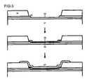
- FIG. 5is a schematic that shows a method of manufacturing an electro-optical element according to the first exemplary embodiment of the present invention
- FIG. 6is a schematic that shows a method of separating and transferring the element chip according to the first exemplary embodiment of the present invention
- FIG. 7is an enlarged schematic showing a transferred element chip according to the first exemplary embodiment of the present invention.
- FIG. 8is a schematic that shows a method of manufacturing an active element and an element chip according to a second exemplary embodiment of the present invention.
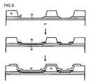
- FIG. 9is a schematic that shows a method of manufacturing an electro-optical element according to the second exemplary embodiment of the present invention.
- FIG. 10is a schematic that shows a method of separating and transferring the element chip according to the second exemplary embodiment of the present invention.
- FIG. 11is an enlarged schematic of a transferred element chip according to the second exemplary embodiment of the present invention.
- FIG. 4shows a method of manufacturing an active element and an element chip according to a first exemplary embodiment.
- the first exemplary embodimentis different from the related art in that, when a first contact hole 4 d is formed, the hole 4 d passes through a underlying insulating film 43 in a portion where an active layer 46 is not formed, and a source and drain metal film is formed. Accordingly, second connection pads 4 k are formed on a surface opposite to the first connection pads 4 j.
- FIG. 5shows a method of manufacturing an electro-optical element according to the first exemplary embodiment of the present invention.
- the electro-optical elementis an organic light-emitting diode.
- An ITO filmis formed on a third substrate 51 to obtain an anode 52 .
- a lyophilic materialis formed as a film and is then opened to obtain lyophilic banks 53 .
- a lyophobic materialis formed as a film and is then opened to obtain lyophobic bank 54 .
- PEDTis selectively applied thereto by an ink-jet method to obtain a hole-carrying layer 55 .
- a light-emitting materialis selectively applied thereon to obtain a light-emitting layer 56 .
- a cathode 57is obtained by depositing a metal having a low work function using a mask.
- FIG. 6shows a method of separating and transferring an element chip according to the first exemplary embodiment of the present invention.
- the adhesiveis an anisotropic conductive paste.
- the first exemplary embodimentis different from the related art in that the anisotropic conductive paste 6 a is applied over a wider area than the element chip 66 on the second substrate 67 , and in that the first substrate 61 and the second substrate 67 are pressed, conductive particles of the anisotropic conductive paste 6 a collapse, and first connection pads 64 of the element chip 66 are electrically connected to connection pads 69 of the second substrate 67 .
- the anisotropic conductive paste 6 aSince the anisotropic conductive paste 6 a is used, the first connection pads 64 of the element chip 66 are connected to the connection pads 69 of the second substrate 67 opposite the first connection pads 64 , but first connection pads 64 of another element chip 66 adjacent to the above-mentioned element chip 64 are not connected to connection pads 69 of the second substrate 67 opposite to the first connection pads 64 . Simultaneously, an anisotropic conductive paste 6 a in the periphery of the element chip 66 is inserted into separations 6 b to reach the first substrate 61 . After the element chip 66 is transferred onto the second substrate 67 by an irradiating laser, the second substrate 67 adheres to the third substrate.
- the anisotropic conductive paste 6 a in the separations 6 bflows along the surface of the element chip 66 facing the third substrate, and conductive particles in the anisotropic conductive paste 6 a collapse to electrically connect the second connection pad 65 of the element chip 66 to the cathode of the third substrate.
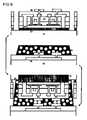
- FIG. 7is an exploded view showing a transferred element chip according to the first exemplary embodiment of the present invention.
- the transferred element chip according to the first exemplary embodimentis different from that of the related art in that first connection pads 73 of an element chip 71 having at least one thin film transistor 72 are electrically connected to connection pads 77 on a second substrate 75 having wiring lines 76 formed thereon by an anisotropic conductive paste 7 b , and in that second connection pads 74 of the element chip 71 having at least one thin film transistor 72 are electrically connected to a cathode 7 a on a third substrate 78 having an organic light-emitting diode formed thereon in the periphery of the element chip 71 by the anisotropic conductive paste 7 b.
- the thin film transistor 72which is an active element, is electrically connected to wiring lines 76 in one surface of the element chip 71 facing the second substrate 75
- the thin film transistor 72which is an active element, is electrically connected to an organic light-emitting diode 79 , which is an electro-optical element, in another surface of the element chip 71 facing the third substrate 78 .
- electrical connectionis performed using an anisotropic conductive paste 7 b of a conductive material.
- the anisotropic conductive paste 7 b of a conductive materialis disposed in a position corresponding to the periphery of the element chip 71 between the second substrate 75 and the element chip 71 .
- the thin film transistor 72which is an active element, is electrically connected to the organic light-emitting diode 79 , which is an electro-optical element, by the anisotropic conductive paste 7 b.
- the second substrate 75is bonded to the third substrate 78 .
- transferring the element chip 71 onto the third substrate 78 , and then adhering the second substrate 75 to the third substrate 78does not depart from the spirit of the present invention.
- any number of elementsis effective within the spirit of the present invention.
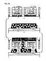
- FIG. 8shows a manufacturing method of an active element and an element chip according to a second exemplary embodiment of the present invention.
- the second exemplary embodimentis different from the first exemplary embodiment in that an opening 81 is simultaneously formed with separations 8 m .
- the opening 81is a hole of the element chip, and only one element chip is shown in FIG. 8 .
- FIG. 9shows a method of manufacturing an electro-optical element according to the second exemplary embodiment of the present invention.
- the second exemplary embodimentis different from the first exemplary embodiment in that a connection pad 98 of a third substrate 91 including a lyophilic bank 93 , a lyophobic bank 94 , and a cathode 97 is formed.
- FIG. 10shows a method of separating and transferring an element chip according to the second exemplary embodiment of the present invention.
- the second exemplary embodimentis different from the first exemplary embodiment in that an anisotropic conductive paste aa is inserted into an opening ab of the element chip a 6 to reach a first substrate a 1 .
- the second substrate a 7adheres to a third substrate.
- the anisotropic conductive paste aa in the opening abflows along the surface of the element chip a 6 facing the third substrate, and conductive particles in the anisotropic conductive paste aa collapse to electrically connect a second connection pad a 5 of the element chip a 6 to a connection pad of the third substrate.
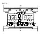
- FIG. 11is an enlarged view of a transferred element chip according to the second exemplary embodiment of the present invention.
- the transferred element chip according to the second exemplary embodimentis different from that of the first exemplary embodiment in that a second connection pad b 4 of an element chip b 1 having at least one thin film transistor b 2 is electrically connected to a connection pad ba on a third substrate b 8 having an organic light-emitting diode b 9 formed thereon by an anisotropic conductive paste bb inserted in the opening of element chip b 1 .
- the thin film transistor b 2which is an active element, is electrically connected to wiring lines b 6 on one surface of the element chip b 1 facing the second substrate b 5
- the thin film transistor b 2which is an active element, is electrically connected to an organic light-emitting diode b 9 , which is an electro-optical element, on another surface of the element chip b 1 facing the third substrate b 8 .
- the electrical connectionis performed using an anisotropic conductive paste bb of a conductive material.
- the thin film transistor b 2which is an active element, is electrically connected to the organic light-emitting diode b 9 which is an electro-optical element.
- the second substrate b 5adheres to the third substrate b 8 .
- transferring the element chip b 1 onto the third substrate b 8 , and then adhering the second substrate b 5 to the third substrate b 8does not depart from the spirit of this invention.
- two first connection pads b 3 of the element chip and two connection pads b 7 on the second substrate corresponding thereto, and one second connection pad b 4 of the element chip and one connection pad ba on the third substrate corresponding theretoare shown in FIG. 11 , any number of elements is available within the spirit of the present invention.
- the present inventioncan be applied to liquid crystal electro-optical devices using an active matrix substrate.
- the active matrix substrate applied to the present invention according to the aforementioned exemplary embodimentscan reduce manufacturing costs and can enhance the quality as compared with an electro-optical device using a related active matrix substrate.
- a liquid crystal electro-optical deviceis used as an electro-optical device, other electro-optical devices, such as an organic light-emitting device and an electrophoresis display device, can be applied.
- the above electro-optical devicesare mounted to electronic apparatuses, such as mobile telephones, and thus the present invention can provide an electronic apparatus having the above advantage.
Landscapes
- Engineering & Computer Science (AREA)
- Computer Hardware Design (AREA)
- Microelectronics & Electronic Packaging (AREA)
- Power Engineering (AREA)
- Physics & Mathematics (AREA)
- Condensed Matter Physics & Semiconductors (AREA)
- General Physics & Mathematics (AREA)
- Manufacturing & Machinery (AREA)
- Liquid Crystal (AREA)
- Electroluminescent Light Sources (AREA)
- Devices For Indicating Variable Information By Combining Individual Elements (AREA)
Abstract
Description
Claims (6)
Applications Claiming Priority (2)
| Application Number | Priority Date | Filing Date | Title |
|---|---|---|---|
| JP2003-019128 | 2003-01-28 | ||
| JP2003019128AJP3972825B2 (en) | 2003-01-28 | 2003-01-28 | Manufacturing method of active matrix display device |
Publications (2)
| Publication Number | Publication Date |
|---|---|
| US20040227886A1 US20040227886A1 (en) | 2004-11-18 |
| US7071488B2true US7071488B2 (en) | 2006-07-04 |
Family
ID=32949086
Family Applications (1)
| Application Number | Title | Priority Date | Filing Date |
|---|---|---|---|
| US10/765,197Expired - LifetimeUS7071488B2 (en) | 2003-01-28 | 2004-01-28 | Active matrix display device and thin film transistor display device |
Country Status (2)
| Country | Link |
|---|---|
| US (1) | US7071488B2 (en) |
| JP (1) | JP3972825B2 (en) |
Cited By (7)
| Publication number | Priority date | Publication date | Assignee | Title |
|---|---|---|---|---|
| US20060270114A1 (en)* | 2003-10-06 | 2006-11-30 | Semiconductor Energy Laboratory Co., Ltd. | Semiconductor device and method for manufacturing the same |
| US20070029554A1 (en)* | 2005-08-05 | 2007-02-08 | Semiconductor Energy Laboratory Co., Ltd. | Light-emitting device and manufacturing method thereof |
| US20100123160A1 (en)* | 2008-11-18 | 2010-05-20 | Semiconductor Energy Laboratory Co., Ltd. | Light-Emitting Device, Method for Manufacturing the Same, and Cellular Phone |
| US20100237354A1 (en)* | 2004-11-22 | 2010-09-23 | Semiconductor Energy Laboratory Co., Ltd. | Semiconductor device and method for manufacturing the same |
| US9189997B2 (en) | 2006-04-14 | 2015-11-17 | Semiconductor Energy Laboratory Co., Ltd. | Display device |
| US10147742B2 (en) | 2009-07-07 | 2018-12-04 | Semiconductor Energy Laboratory Co., Ltd. | Display device |
| US10991784B2 (en)* | 2016-04-07 | 2021-04-27 | Samsung Display Co., Ltd. | Transistor display panel including lower electrode disposed under semiconductor and display device including the same |
Families Citing this family (10)
| Publication number | Priority date | Publication date | Assignee | Title |
|---|---|---|---|---|
| JP5072208B2 (en)* | 2004-09-24 | 2012-11-14 | 株式会社半導体エネルギー研究所 | Method for manufacturing semiconductor device |
| JP4742588B2 (en)* | 2004-09-29 | 2011-08-10 | セイコーエプソン株式会社 | ORGANIC EL DEVICE, ITS MANUFACTURING METHOD, AND ELECTRONIC DEVICE |
| JP5072217B2 (en)* | 2004-11-22 | 2012-11-14 | 株式会社半導体エネルギー研究所 | Method for manufacturing semiconductor device |
| WO2007108371A1 (en)* | 2006-03-15 | 2007-09-27 | Semiconductor Energy Laboratory Co., Ltd. | Semiconductor device |
| US9161448B2 (en) | 2010-03-29 | 2015-10-13 | Semprius, Inc. | Laser assisted transfer welding process |
| WO2011126726A1 (en)* | 2010-03-29 | 2011-10-13 | Semprius, Inc. | Electrically bonded arrays of transfer printed active components |
| US9412727B2 (en) | 2011-09-20 | 2016-08-09 | Semprius, Inc. | Printing transferable components using microstructured elastomeric surfaces with pressure modulated reversible adhesion |
| US9358775B2 (en) | 2014-07-20 | 2016-06-07 | X-Celeprint Limited | Apparatus and methods for micro-transfer-printing |
| US9704821B2 (en) | 2015-08-11 | 2017-07-11 | X-Celeprint Limited | Stamp with structured posts |
| US10748793B1 (en) | 2019-02-13 | 2020-08-18 | X Display Company Technology Limited | Printing component arrays with different orientations |
Citations (29)
| Publication number | Priority date | Publication date | Assignee | Title |
|---|---|---|---|---|
| US5789763A (en)* | 1993-07-30 | 1998-08-04 | Ag Technology Co., Ltd. | Substrate for a display device, a TFT display element using the substrate |
| JP2001282423A (en) | 2000-03-29 | 2001-10-12 | Aiwa Co Ltd | Key operation processing method and key operation processor |
| JP2001282424A (en) | 2000-03-29 | 2001-10-12 | Seiko Epson Corp | Presentation system and wireless remote control |
| US20010040645A1 (en)* | 2000-02-01 | 2001-11-15 | Shunpei Yamazaki | Semiconductor device and manufacturing method thereof |
| US20020079493A1 (en)* | 2000-11-07 | 2002-06-27 | Masakazu Morishita | Radiation image pick-up device |
| JP2002314123A (en) | 2001-04-18 | 2002-10-25 | Sony Corp | Method of transferring element, method of arranging element using it, and method of manufacturing image display device |
| JP2002311858A (en) | 2001-04-19 | 2002-10-25 | Sony Corp | Element transfer method, element arrangement method using the same, and image display device manufacturing method |
| JP2002314052A (en) | 2001-04-11 | 2002-10-25 | Sony Corp | Element transfer method, element arrangement method using the same, and image display device manufacturing method |
| US20020173085A1 (en)* | 2001-05-18 | 2002-11-21 | Semiconductor Energy Laboratory Co., Ltd. & Sharp Kabushiki Kaisha | Method of manufacturing a semiconductor device and semiconductor manufacturing apparatus |
| JP2002343944A (en) | 2001-05-14 | 2002-11-29 | Sony Corp | Transferring method of electronic part, arraying method of element, and manufacturing method of image display device |
| US6492659B1 (en)* | 1999-05-15 | 2002-12-10 | Semiconductor Energy Laboratory Co., Ltd. | Semiconductor device having single crystal grains with hydrogen and tapered gate insulation layer |
| JP2002368282A (en) | 2001-06-05 | 2002-12-20 | Sony Corp | Method of transferring element and method of arranging element using the same, and method of manufacturing image display |
| US20030011870A1 (en)* | 2001-06-20 | 2003-01-16 | Toshihiro Otake | Mask, substrate with light reflection film, manufacturing method for light reflection film, manufacturing method for electro-optical device and electro-optical device, and electronic apparatus |
| US20030011738A1 (en)* | 2001-07-10 | 2003-01-16 | Masahiko Akiyama | Active matrix substrated and method of manufacturing the same |
| US20030027369A1 (en)* | 2001-07-03 | 2003-02-06 | Semiconductor Energy Laboratory Co., Ltd. | Light-emitting device, method of manufacturing a light-emitting device, and electronic equipment |
| US20030034497A1 (en)* | 2001-06-20 | 2003-02-20 | Semiconductor Energy Laboratory Co., Ltd. | Light emitting device and method of manufacturing the same |
| JP2003077940A (en) | 2001-09-06 | 2003-03-14 | Sony Corp | Device transfer method, device array method using the same, and image display device manufacturing method |
| US6541294B1 (en)* | 1999-07-22 | 2003-04-01 | Semiconductor Energy Laboratory Co., Ltd. | Semiconductor device and manufacturing method thereof |
| US6559916B1 (en)* | 1995-07-19 | 2003-05-06 | Sony Corporation | Reflective guest-host liquid-crystal display device |
| JP2003133708A (en) | 2001-10-30 | 2003-05-09 | Sony Corp | Electronic component and transfer method thereof, circuit board and manufacturing method thereof, and display and manufacturing method thereof |
| US20030094615A1 (en)* | 2001-11-16 | 2003-05-22 | Semiconductor Energy Laboratory Co., Ltd. | Light emitting device |
| US6593591B2 (en)* | 1996-05-15 | 2003-07-15 | Seiko Epson Corporation | Thin film device provided with coating film, liquid crystal panel and electronic device, and method the thin film device |
| US20030132446A1 (en)* | 2002-01-15 | 2003-07-17 | Ewald Guenther | Multi substrate organic light emitting devices |
| US6605826B2 (en)* | 2000-08-18 | 2003-08-12 | Semiconductor Energy Laboratory Co., Ltd. | Light-emitting device and display device |
| JP2003258210A (en) | 2001-12-27 | 2003-09-12 | Canon Inc | Display device and method of manufacturing the same |
| US6798132B2 (en)* | 2001-04-23 | 2004-09-28 | Semiconductor Energy Laboratory Co., Ltd. | Display device and method of manufacturing the same |
| US6911675B2 (en)* | 2001-11-30 | 2005-06-28 | Semiconductor Energy Laboratory Co., Ltd. | Active matrix display device and manufacturing method thereof |
| US20050175792A1 (en)* | 2001-03-29 | 2005-08-11 | Akitoshi Maeda | Liquid crystal display panel having reflection electrodes improved in smooth surface morphology and process for fabrication thereof |
| US6992439B2 (en)* | 2001-02-22 | 2006-01-31 | Semiconductor Energy Laboratory Co., Ltd. | Display device with sealing structure for protecting organic light emitting element |
- 2003
- 2003-01-28JPJP2003019128Apatent/JP3972825B2/ennot_activeExpired - Fee Related
- 2004
- 2004-01-28USUS10/765,197patent/US7071488B2/ennot_activeExpired - Lifetime
Patent Citations (31)
| Publication number | Priority date | Publication date | Assignee | Title |
|---|---|---|---|---|
| US5789763A (en)* | 1993-07-30 | 1998-08-04 | Ag Technology Co., Ltd. | Substrate for a display device, a TFT display element using the substrate |
| US6559916B1 (en)* | 1995-07-19 | 2003-05-06 | Sony Corporation | Reflective guest-host liquid-crystal display device |
| US6593591B2 (en)* | 1996-05-15 | 2003-07-15 | Seiko Epson Corporation | Thin film device provided with coating film, liquid crystal panel and electronic device, and method the thin film device |
| US20030092213A1 (en)* | 1999-05-15 | 2003-05-15 | Semiconductor Energy Laboratory Co., Ltd. | Semiconductor device and method for its fabrication |
| US6492659B1 (en)* | 1999-05-15 | 2002-12-10 | Semiconductor Energy Laboratory Co., Ltd. | Semiconductor device having single crystal grains with hydrogen and tapered gate insulation layer |
| US6541294B1 (en)* | 1999-07-22 | 2003-04-01 | Semiconductor Energy Laboratory Co., Ltd. | Semiconductor device and manufacturing method thereof |
| US20010040645A1 (en)* | 2000-02-01 | 2001-11-15 | Shunpei Yamazaki | Semiconductor device and manufacturing method thereof |
| JP2001282424A (en) | 2000-03-29 | 2001-10-12 | Seiko Epson Corp | Presentation system and wireless remote control |
| JP2001282423A (en) | 2000-03-29 | 2001-10-12 | Aiwa Co Ltd | Key operation processing method and key operation processor |
| US6605826B2 (en)* | 2000-08-18 | 2003-08-12 | Semiconductor Energy Laboratory Co., Ltd. | Light-emitting device and display device |
| US20020079493A1 (en)* | 2000-11-07 | 2002-06-27 | Masakazu Morishita | Radiation image pick-up device |
| US6992439B2 (en)* | 2001-02-22 | 2006-01-31 | Semiconductor Energy Laboratory Co., Ltd. | Display device with sealing structure for protecting organic light emitting element |
| US20050175792A1 (en)* | 2001-03-29 | 2005-08-11 | Akitoshi Maeda | Liquid crystal display panel having reflection electrodes improved in smooth surface morphology and process for fabrication thereof |
| JP2002314052A (en) | 2001-04-11 | 2002-10-25 | Sony Corp | Element transfer method, element arrangement method using the same, and image display device manufacturing method |
| JP2002314123A (en) | 2001-04-18 | 2002-10-25 | Sony Corp | Method of transferring element, method of arranging element using it, and method of manufacturing image display device |
| JP2002311858A (en) | 2001-04-19 | 2002-10-25 | Sony Corp | Element transfer method, element arrangement method using the same, and image display device manufacturing method |
| US6798132B2 (en)* | 2001-04-23 | 2004-09-28 | Semiconductor Energy Laboratory Co., Ltd. | Display device and method of manufacturing the same |
| JP2002343944A (en) | 2001-05-14 | 2002-11-29 | Sony Corp | Transferring method of electronic part, arraying method of element, and manufacturing method of image display device |
| US20020173085A1 (en)* | 2001-05-18 | 2002-11-21 | Semiconductor Energy Laboratory Co., Ltd. & Sharp Kabushiki Kaisha | Method of manufacturing a semiconductor device and semiconductor manufacturing apparatus |
| JP2002368282A (en) | 2001-06-05 | 2002-12-20 | Sony Corp | Method of transferring element and method of arranging element using the same, and method of manufacturing image display |
| US20030034497A1 (en)* | 2001-06-20 | 2003-02-20 | Semiconductor Energy Laboratory Co., Ltd. | Light emitting device and method of manufacturing the same |
| US20030011870A1 (en)* | 2001-06-20 | 2003-01-16 | Toshihiro Otake | Mask, substrate with light reflection film, manufacturing method for light reflection film, manufacturing method for electro-optical device and electro-optical device, and electronic apparatus |
| US6849877B2 (en)* | 2001-06-20 | 2005-02-01 | Semiconductor Energy Laboratory Co., Ltd. | Light emitting device and method of manufacturing the same |
| US20030027369A1 (en)* | 2001-07-03 | 2003-02-06 | Semiconductor Energy Laboratory Co., Ltd. | Light-emitting device, method of manufacturing a light-emitting device, and electronic equipment |
| US20030011738A1 (en)* | 2001-07-10 | 2003-01-16 | Masahiko Akiyama | Active matrix substrated and method of manufacturing the same |
| JP2003077940A (en) | 2001-09-06 | 2003-03-14 | Sony Corp | Device transfer method, device array method using the same, and image display device manufacturing method |
| JP2003133708A (en) | 2001-10-30 | 2003-05-09 | Sony Corp | Electronic component and transfer method thereof, circuit board and manufacturing method thereof, and display and manufacturing method thereof |
| US20030094615A1 (en)* | 2001-11-16 | 2003-05-22 | Semiconductor Energy Laboratory Co., Ltd. | Light emitting device |
| US6911675B2 (en)* | 2001-11-30 | 2005-06-28 | Semiconductor Energy Laboratory Co., Ltd. | Active matrix display device and manufacturing method thereof |
| JP2003258210A (en) | 2001-12-27 | 2003-09-12 | Canon Inc | Display device and method of manufacturing the same |
| US20030132446A1 (en)* | 2002-01-15 | 2003-07-17 | Ewald Guenther | Multi substrate organic light emitting devices |
Non-Patent Citations (4)
| Title |
|---|
| Shimoda et al., "Surface Free Technology by Laser Annealing (SUFTLA)" IEEE, 1999, pp. 289-292. |
| Shimoda, "Future Trend of TFTs", Asia Display/IDW '01 , pp. 327-330. |
| Utsunomiya et al., "Low Temperature Poly-Si TFT-LCD Transferred onto Plastic Substrate Using Surface Free Technology by Laser Ablation/Annealing (SUFTLA(R))", Asia Display/IDW '01, pp. 339-342. |
| Utsunomiya et al., Low Temperature Poly-Si TFTs on Plastic Substrate Using Surface Free Technology by Laser Ablation/Annealing (SUFTLA(TM)), SID 00 Digest, 2000, pp. 916-919. |
Cited By (29)
| Publication number | Priority date | Publication date | Assignee | Title |
|---|---|---|---|---|
| US7180197B2 (en) | 2003-10-06 | 2007-02-20 | Semiconductor Energy Laboratory Co., Ltd. | Semiconductor device containing stacked semiconductor chips and manufacturing method thereof |
| US20060270114A1 (en)* | 2003-10-06 | 2006-11-30 | Semiconductor Energy Laboratory Co., Ltd. | Semiconductor device and method for manufacturing the same |
| US8481370B2 (en) | 2003-10-06 | 2013-07-09 | Semiconductor Energy Laboratory Co., Ltd. | Semiconductor device and method for manufacturing the same |
| US20100237354A1 (en)* | 2004-11-22 | 2010-09-23 | Semiconductor Energy Laboratory Co., Ltd. | Semiconductor device and method for manufacturing the same |
| US8546210B2 (en)* | 2004-11-22 | 2013-10-01 | Semiconductor Energy Laboratory Co., Ltd. | Semiconductor device and method for manufacturing the same |
| US20070029554A1 (en)* | 2005-08-05 | 2007-02-08 | Semiconductor Energy Laboratory Co., Ltd. | Light-emitting device and manufacturing method thereof |
| US8138502B2 (en) | 2005-08-05 | 2012-03-20 | Semiconductor Energy Laboratory Co., Ltd. | Light-emitting device and manufacturing method thereof |
| US8497512B2 (en) | 2005-08-05 | 2013-07-30 | Semiconductor Energy Laboratory Co., Ltd. | Light-emitting device and manufacturing method thereof |
| US9189997B2 (en) | 2006-04-14 | 2015-11-17 | Semiconductor Energy Laboratory Co., Ltd. | Display device |
| US11289558B2 (en) | 2008-11-18 | 2022-03-29 | Semiconductor Energy Laboratory Co., Ltd. | Light-emitting device, method for manufacturing the same, and cellular phone |
| US10896941B2 (en) | 2008-11-18 | 2021-01-19 | Semiconductor Energy Laboratory Co., Ltd. | Light-emitting device, method for manufacturing the same, and cellular phone |
| US12200983B2 (en) | 2008-11-18 | 2025-01-14 | Semiconductor Energy Laboratory Co., Ltd. | Light-emitting device, method for manufacturing the same, and cellular phone |
| US10269883B2 (en) | 2008-11-18 | 2019-04-23 | Semiconductor Energy Laboratory Co., Ltd. | Light-emitting device method for manufacturing the same, and cellular phone |
| US11818925B2 (en) | 2008-11-18 | 2023-11-14 | Semiconductor Energy Laboratory Co., Ltd. | Light-emitting device, method for manufacturing the same, and cellular phone |
| US20100123160A1 (en)* | 2008-11-18 | 2010-05-20 | Semiconductor Energy Laboratory Co., Ltd. | Light-Emitting Device, Method for Manufacturing the Same, and Cellular Phone |
| US10600853B2 (en) | 2008-11-18 | 2020-03-24 | Semiconductor Energy Laboratory Co., Ltd. | Light-emitting device, method for manufacturing the same, and cellular phone |
| US8610155B2 (en)* | 2008-11-18 | 2013-12-17 | Semiconductor Energy Laboratory Co., Ltd. | Light-emitting device, method for manufacturing the same, and cellular phone |
| US10985186B1 (en) | 2009-07-07 | 2021-04-20 | Semiconductor Energy Laboratory Co., Ltd. | Display device |
| US10692891B2 (en) | 2009-07-07 | 2020-06-23 | Semiconductor Energy Laboratory Co., Ltd. | Display device |
| US11018159B2 (en) | 2009-07-07 | 2021-05-25 | Semiconductor Energy Laboratory Co., Ltd. | Display device |
| US10411038B2 (en) | 2009-07-07 | 2019-09-10 | Semiconductor Energy Laboratory Co., Ltd. | Display device |
| US11476280B2 (en) | 2009-07-07 | 2022-10-18 | Semiconductor Energy Laboratory Co., Ltd. | Display device |
| US10361221B2 (en) | 2009-07-07 | 2019-07-23 | Semiconductor Energy Laboratory Co., Ltd. | Display device |
| US11824060B2 (en) | 2009-07-07 | 2023-11-21 | Semiconductor Energy Laboratory Co., Ltd. | Display device |
| US12100708B2 (en) | 2009-07-07 | 2024-09-24 | Semiconductor Energy Laboratory Co., Ltd. | Display device |
| US10147742B2 (en) | 2009-07-07 | 2018-12-04 | Semiconductor Energy Laboratory Co., Ltd. | Display device |
| US10991784B2 (en)* | 2016-04-07 | 2021-04-27 | Samsung Display Co., Ltd. | Transistor display panel including lower electrode disposed under semiconductor and display device including the same |
| US11751433B2 (en) | 2016-04-07 | 2023-09-05 | Samsung Display Co., Ltd. | Transistor display panel including lower electrode disposed under a semiconductor and display device including the same |
| US12310181B2 (en) | 2016-04-07 | 2025-05-20 | Samsung Display Co., Ltd. | Transistor array panel, manufacturing method thereof, and display device including the same |
Also Published As
| Publication number | Publication date |
|---|---|
| US20040227886A1 (en) | 2004-11-18 |
| JP2004233444A (en) | 2004-08-19 |
| JP3972825B2 (en) | 2007-09-05 |
Similar Documents
| Publication | Publication Date | Title |
|---|---|---|
| US7071488B2 (en) | Active matrix display device and thin film transistor display device | |
| US7824952B2 (en) | Display apparatus and method of manufacturing thereof | |
| US6927464B2 (en) | Flat panel display device | |
| CN100424576C (en) | Active matrix display device and manufacturing method thereof | |
| US7888674B2 (en) | Thin-film transistor substrate and method of manufacturing the same | |
| US8182301B2 (en) | Method of fabricating flat panel display having pad electrode | |
| US8415666B2 (en) | Thin film transistor substrate having thin film transistors with improved etching characteristics, method of manufacturing the same, and display apparatus having the same | |
| US7208873B2 (en) | Organic electroluminescence display device and method for fabricating the same | |
| US7341894B2 (en) | Semiconductor, electrooptic apparatus and electronic apparatus | |
| US11929358B2 (en) | Display backplate and method for manufacturing same, display panel and method for manufacturing same, and display device | |
| US8704305B2 (en) | Thin film transistor | |
| US20020164860A1 (en) | Method of fabricating thin-film transistor | |
| JP3820743B2 (en) | Active matrix substrate, method of manufacturing active matrix substrate, and display device | |
| EP1675195A3 (en) | Organic thin film transistor for an OLED display | |
| KR100848100B1 (en) | Thin film transistor substrate and manufacturing method thereof | |
| KR102740407B1 (en) | Array substrate, display device, and method for manufacturing array substrate | |
| US7923293B2 (en) | Method for manufacturing a semiconductor device wherein the electrical connection between two components is provided by capillary phenomenon of a liquid conductor material in a cavity therebetween | |
| US7151044B2 (en) | Thin film transistor type display device, method of manufacturing thin film element, thin film transistor circuit board, electro-optical device, and electronic apparatus | |
| US20060258033A1 (en) | Active matrix substrate and method for fabricating the same |
Legal Events
| Date | Code | Title | Description |
|---|---|---|---|
| AS | Assignment | Owner name:SEIKO EPSON CORPORATION, JAPAN Free format text:ASSIGNMENT OF ASSIGNORS INTEREST;ASSIGNOR:KIMURA, MUTSUMI;REEL/FRAME:014840/0089 Effective date:20040225 | |
| STCF | Information on status: patent grant | Free format text:PATENTED CASE | |
| FEPP | Fee payment procedure | Free format text:PAYOR NUMBER ASSIGNED (ORIGINAL EVENT CODE: ASPN); ENTITY STATUS OF PATENT OWNER: LARGE ENTITY | |
| FPAY | Fee payment | Year of fee payment:4 | |
| FPAY | Fee payment | Year of fee payment:8 | |
| MAFP | Maintenance fee payment | Free format text:PAYMENT OF MAINTENANCE FEE, 12TH YEAR, LARGE ENTITY (ORIGINAL EVENT CODE: M1553) Year of fee payment:12 | |
| AS | Assignment | Owner name:EL TECHNOLOGY FUSION GODO KAISHA, JAPAN Free format text:ASSIGNMENT OF ASSIGNORS INTEREST;ASSIGNOR:SEIKO EPSON CORPORATION;REEL/FRAME:047998/0879 Effective date:20181012 | |
| AS | Assignment | Owner name:ELEMENT CAPITAL COMMERCIAL COMPANY PTE. LTD., SINGAPORE Free format text:ASSIGNMENT OF ASSIGNORS INTEREST;ASSIGNOR:EL TECHNOLOGY FUSION GODO KAISHA;REEL/FRAME:059912/0458 Effective date:20211228 |