US7064980B2 - Non-volatile memory and method with bit line coupled compensation - Google Patents
Non-volatile memory and method with bit line coupled compensationDownload PDFInfo
- Publication number
- US7064980B2 US7064980B2US10/667,222US66722203AUS7064980B2US 7064980 B2US7064980 B2US 7064980B2US 66722203 AUS66722203 AUS 66722203AUS 7064980 B2US7064980 B2US 7064980B2
- Authority
- US
- United States
- Prior art keywords
- memory storage
- program
- storage units
- page
- memory
- Prior art date
- Legal status (The legal status is an assumption and is not a legal conclusion. Google has not performed a legal analysis and makes no representation as to the accuracy of the status listed.)
- Expired - Lifetime, expires
Links
- 238000000034methodMethods0.000titleclaimsabstractdescription26
- 230000005055memory storageEffects0.000claimsabstractdescription91
- 238000007667floatingMethods0.000claimsdescription51
- 230000008878couplingEffects0.000abstractdescription32
- 238000010168coupling processMethods0.000abstractdescription32
- 238000005859coupling reactionMethods0.000abstractdescription32
- 210000004027cellAnatomy0.000description75
- 230000000694effectsEffects0.000description12
- 239000003990capacitorSubstances0.000description9
- 238000010586diagramMethods0.000description8
- 230000005764inhibitory processEffects0.000description7
- 230000002401inhibitory effectEffects0.000description6
- 239000000758substrateSubstances0.000description6
- 101000615747Homo sapiens tRNA-splicing endonuclease subunit Sen2Proteins0.000description4
- 230000007246mechanismEffects0.000description4
- 102100021774tRNA-splicing endonuclease subunit Sen2Human genes0.000description4
- 230000005641tunnelingEffects0.000description4
- 239000004065semiconductorSubstances0.000description3
- VYPSYNLAJGMNEJ-UHFFFAOYSA-NSilicium dioxideChemical compoundO=[Si]=OVYPSYNLAJGMNEJ-UHFFFAOYSA-N0.000description2
- 230000008859changeEffects0.000description2
- 230000001447compensatory effectEffects0.000description2
- 230000001419dependent effectEffects0.000description2
- 230000002349favourable effectEffects0.000description2
- 230000006870functionEffects0.000description2
- 239000002784hot electronSubstances0.000description2
- 238000002347injectionMethods0.000description2
- 239000007924injectionSubstances0.000description2
- 238000002955isolationMethods0.000description2
- 238000005192partitionMethods0.000description2
- 230000002093peripheral effectEffects0.000description2
- 230000003094perturbing effectEffects0.000description2
- 230000005855radiationEffects0.000description2
- 210000000352storage cellAnatomy0.000description2
- 230000005689Fowler Nordheim tunnelingEffects0.000description1
- 239000008186active pharmaceutical agentSubstances0.000description1
- 230000001154acute effectEffects0.000description1
- 238000013459approachMethods0.000description1
- 238000012937correctionMethods0.000description1
- 238000013500data storageMethods0.000description1
- 238000001514detection methodMethods0.000description1
- 239000003989dielectric materialSubstances0.000description1
- 238000009792diffusion processMethods0.000description1
- 238000007599dischargingMethods0.000description1
- 230000005684electric fieldEffects0.000description1
- 238000005516engineering processMethods0.000description1
- 230000005669field effectEffects0.000description1
- 238000010348incorporationMethods0.000description1
- 230000010354integrationEffects0.000description1
- 238000004519manufacturing processMethods0.000description1
- 230000008569processEffects0.000description1
- 239000013643reference controlSubstances0.000description1
- 230000000717retained effectEffects0.000description1
- 238000000926separation methodMethods0.000description1
- 235000012239silicon dioxideNutrition0.000description1
- 239000000377silicon dioxideSubstances0.000description1
- 239000000243solutionSubstances0.000description1
- 238000000638solvent extractionMethods0.000description1
- 238000012360testing methodMethods0.000description1
- 238000012546transferMethods0.000description1
Images


Classifications
- G—PHYSICS
- G11—INFORMATION STORAGE
- G11C—STATIC STORES
- G11C16/00—Erasable programmable read-only memories
- G11C16/02—Erasable programmable read-only memories electrically programmable
- G11C16/06—Auxiliary circuits, e.g. for writing into memory
- G11C16/10—Programming or data input circuits
- G11C16/12—Programming voltage switching circuits
- G—PHYSICS
- G11—INFORMATION STORAGE
- G11C—STATIC STORES
- G11C11/00—Digital stores characterised by the use of particular electric or magnetic storage elements; Storage elements therefor
- G11C11/56—Digital stores characterised by the use of particular electric or magnetic storage elements; Storage elements therefor using storage elements with more than two stable states represented by steps, e.g. of voltage, current, phase, frequency
- G11C11/5621—Digital stores characterised by the use of particular electric or magnetic storage elements; Storage elements therefor using storage elements with more than two stable states represented by steps, e.g. of voltage, current, phase, frequency using charge storage in a floating gate
- G11C11/5628—Programming or writing circuits; Data input circuits
- G—PHYSICS
- G11—INFORMATION STORAGE
- G11C—STATIC STORES
- G11C11/00—Digital stores characterised by the use of particular electric or magnetic storage elements; Storage elements therefor
- G11C11/56—Digital stores characterised by the use of particular electric or magnetic storage elements; Storage elements therefor using storage elements with more than two stable states represented by steps, e.g. of voltage, current, phase, frequency
- G11C11/5621—Digital stores characterised by the use of particular electric or magnetic storage elements; Storage elements therefor using storage elements with more than two stable states represented by steps, e.g. of voltage, current, phase, frequency using charge storage in a floating gate
- G11C11/5642—Sensing or reading circuits; Data output circuits
- G—PHYSICS
- G11—INFORMATION STORAGE
- G11C—STATIC STORES
- G11C16/00—Erasable programmable read-only memories
- G11C16/02—Erasable programmable read-only memories electrically programmable
- G11C16/04—Erasable programmable read-only memories electrically programmable using variable threshold transistors, e.g. FAMOS
- G11C16/0483—Erasable programmable read-only memories electrically programmable using variable threshold transistors, e.g. FAMOS comprising cells having several storage transistors connected in series
- G—PHYSICS
- G11—INFORMATION STORAGE
- G11C—STATIC STORES
- G11C16/00—Erasable programmable read-only memories
- G11C16/02—Erasable programmable read-only memories electrically programmable
- G11C16/06—Auxiliary circuits, e.g. for writing into memory
- G11C16/10—Programming or data input circuits
- G—PHYSICS
- G11—INFORMATION STORAGE
- G11C—STATIC STORES
- G11C16/00—Erasable programmable read-only memories
- G11C16/02—Erasable programmable read-only memories electrically programmable
- G11C16/06—Auxiliary circuits, e.g. for writing into memory
- G11C16/24—Bit-line control circuits
- G—PHYSICS
- G11—INFORMATION STORAGE
- G11C—STATIC STORES
- G11C16/00—Erasable programmable read-only memories
- G11C16/02—Erasable programmable read-only memories electrically programmable
- G11C16/06—Auxiliary circuits, e.g. for writing into memory
- G11C16/34—Determination of programming status, e.g. threshold voltage, overprogramming or underprogramming, retention
- G11C16/3418—Disturbance prevention or evaluation; Refreshing of disturbed memory data
- G11C16/3427—Circuits or methods to prevent or reduce disturbance of the state of a memory cell when neighbouring cells are read or written
- G—PHYSICS
- G11—INFORMATION STORAGE
- G11C—STATIC STORES
- G11C16/00—Erasable programmable read-only memories
- G11C16/02—Erasable programmable read-only memories electrically programmable
- G11C16/06—Auxiliary circuits, e.g. for writing into memory
- G11C16/34—Determination of programming status, e.g. threshold voltage, overprogramming or underprogramming, retention
- G11C16/3436—Arrangements for verifying correct programming or erasure
- G11C16/3468—Prevention of overerasure or overprogramming, e.g. by verifying whilst erasing or writing
Definitions
- This inventionrelates generally to non-volatile semiconductor memory such as electrically erasable programmable read-only memory (EEPROM) and flash EEPROM, and specifically ones having improved programming and sensing circuits for a page of contiguous row of charge storage units.
- EEPROMelectrically erasable programmable read-only memory
- flash EEPROMflash EEPROM
- Solid-state memorycapable of non-volatile storage of charge, particularly in the form of EEPROM and flash EEPROM packaged as a small form factor card, has recently become the storage of choice in a variety of mobile and handheld devices, notably information appliances and consumer electronics products.
- RAMrandom access memory
- flash memoryis non-volatile, retaining its stored data even after power is turned off.
- flash memoryis increasingly being used in mass storage applications.
- Conventional mass storage, based on rotating magnetic medium such as hard drives and floppy disks,is unsuitable for the mobile and handheld environment. This is because disk drives tend to be bulky, are prone to mechanical failure and have high latency and high power requirements.
- flash memoryboth embedded and in the form of a removable card is ideally suited in the mobile and handheld environment because of its small size, low power consumption, high speed and high reliability features.
- EEPROM and electrically programmable read-only memoryare non-volatile memory that can be erased and have new data written or “programmed” into their memory cells. Both utilize a floating (unconnected) conductive gate, in a field effect transistor structure, positioned over a channel region in a semiconductor substrate, between source and drain regions. A control gate is then provided over the floating gate. The threshold voltage characteristic of the transistor is controlled by the amount of charge that is retained on the floating gate. That is, for a given level of charge on the floating gate, there is a corresponding voltage (threshold) that must be applied to the control gate before the transistor is turned “on” to permit conduction between its source and drain regions.
- threshold voltage characteristic of the transistoris controlled by the amount of charge that is retained on the floating gate. That is, for a given level of charge on the floating gate, there is a corresponding voltage (threshold) that must be applied to the control gate before the transistor is turned “on” to permit conduction between its source and drain regions.
- the floating gatecan hold a range of charges and therefore can be programmed to any threshold voltage level within a threshold voltage window.
- the size of the threshold voltage windowis delimited by the minimum and maximum threshold levels of the device, which in turn correspond to the range of the charges that can be programmed onto the floating gate.
- the threshold windowgenerally depends on the memory device's characteristics, operating conditions and history. Each distinct, resolvable threshold voltage level range within the window may, in principle, be used to designate a definite memory state of the cell.
- the transistor serving as a memory cellis typically programmed to a “programmed” state by one of two mechanisms.
- hot electron injectiona high voltage applied to the drain accelerates electrons across the substrate channel region.
- control gatepulls the hot electrons through a thin gate dielectric onto the floating gate.
- tunnel injectiona high voltage is applied to the control gate relative to the substrate. In this way, electrons are pulled from the substrate to the intervening floating gate.
- the memory devicemay be erased by a number of mechanisms.
- EPROMthe memory is bulk erasable by removing the charge from the floating gate by ultraviolet radiation.
- EEPROMa memory cell is electrically erasable, by applying a high voltage to the substrate relative to the control gate so as to induce electrons in the floating gate to tunnel through a thin oxide to the substrate channel region (i.e., Fowler-Nordheim tunneling).
- the EEPROMis erasable byte by byte.
- flash EEPROMthe memory is electrically erasable either all at once or one or more blocks at a time, where a block may consist of 512 bytes or more of memory.
- the memory devicestypically comprise one or more memory chips that may be mounted on a card.
- Each memory chipcomprises an array of memory cells supported by peripheral circuits such as decoders and erase, write and read circuits.
- peripheral circuitssuch as decoders and erase, write and read circuits.
- the more sophisticated memory devicesalso come with a controller that performs intelligent and higher level memory operations and interfacing.
- non-volatile solid-state memory devicesmay employ different types of memory cells, each type having one or more charge storage unit.
- FIG. 1illustrates schematically a non-volatile memory cell in the form of an EEPROM cell. It has a charge storage unit in the form of a floating gate.
- An electrically erasable and programmable read-only memory (EEPROM)has a similar structure to EPROM, but additionally provides a mechanism for loading and removing charge electrically from its floating gate upon application of proper voltages without the need for exposure to UV radiation. Examples of such cells and methods of manufacturing them are given in U.S. Pat. No. 5,595,924.
- FIG. 2illustrates schematically a string of charge storage units organized into a NAND cell or string.
- a pair of select transistors S 1 , S 2controls the memory transistors chain's connection to the external via the NAND cell's source terminal 54 and drain terminal 56 .
- the source select transistor S 1is turned on by the signal SGS, the source terminal is coupled to a source line.
- the drain select transistor S 2is turned on by the signal SGD, the drain terminal of the NAND cell is coupled to a bit line of the memory array.
- Each memory transistor in the chainhas a charge storage unit to store a given amount of charge so as to represent an intended memory state. Between each source and drain of each memory transistor is a channel region. Voltage on a control gate on each memory transistor, such as 60 , 62 , . . . , 64 controls current conduction in the channel of the memory transistors M 1 , M 2 , . . . , Mn respectively.
- the select transistors S 1 , S 2provides control access to the NAND cell via its source terminal 54 and drain terminal 56 respectively and each is turned on by appropriate voltage to its control gate.
- Non-volatile memoryhas each of its charge storage units in the form of a dielectric layer.
- a dielectric layeris used.
- Such memory devices utilizing dielectric storage elementhave been described by Eitan et al., “NROM: A Novel Localized Trapping, 2-Bit Non-volatile Memory Cell,” IEEE Electron Device Letters, vol. 21, no. 11, November 2000, pp. 543-545.
- An ONO dielectric layerextends across the channel between source and drain diffusions. The charge for one data bit is localized in the dielectric layer adjacent to the drain, and the charge for the other data bit is localized in the dielectric layer adjacent to the source.
- U.S. Pat. Nos. 5,768,192 and 6,011,725disclose a non-volatile memory cell having a trapping dielectric sandwiched between two silicon dioxide layers. Multi-state data storage is implemented by separately reading the binary states of the spatially separated charge storage regions within the dielectric.
- a memory devicetypically comprises of a two-dimensional array of memory cells arranged in rows and columns and addressable by word lines and bit lines.
- FIG. 3illustrates an example of an array of NAND cells, such as that shown in FIG. 2 .
- a bit line 36is coupled to the drain terminal 56 of each NAND cell.
- a source line 34may connect all their source terminals 54 .
- the control gates 60 , . . . , 64 of the NAND cells along a roware connected to a series of corresponding word lines.
- An entire row of NAND cellscan be addressed by turning on the pair of select transistors (see FIG. 2 ) with appropriate voltages on their control gates SGD and SGS via the connected word lines.
- Erase circuitsare provided to erase one or more blocks of memory cells.
- a non-volatile memorysuch as EEPROM is referred to as a “Flash” EEPROM when an entire array of cells, or significant groups of cells of the array, is electrically erased together (i.e., in a flash). Once erased, the group of cells can then be reprogrammed.
- the group of cells erasable togethermay consist of one or more addressable erase unit.
- the erase unit or blocktypically stores one or more pages of data, the page being the unit of programming and reading, although more than one page may be programmed or read in a single operation.
- Each pagetypically stores one or more erase blocks of data, the size of the erase block being defined by the host system.
- An exampleis an erase block of 512 bytes of user data, following a standard established with magnetic disk drives, plus some number of bytes of overhead information about the user data and/or the block in with it is stored. In other systems, the erase block size can be much larger than 512 bytes.
- At least one current breakpoint levelis established so as to partition the conduction window into two regions.
- a cellWhen a cell is read by applying predetermined, fixed voltages, its source/drain current is resolved into a memory state by comparing with the breakpoint level (or reference current I REF ). If the current read is higher than that of the breakpoint level or I REF , the cell is determined to be in one logical state (e.g., a “zero” state). On the other hand, if the current is less than that of the breakpoint level, the cell is determined to be in the other logical state (e.g., a “one” state). Thus, such a two-state cell stores one bit of digital information.
- a reference current sourcewhich may be externally programmable, is often provided as part of a memory system to generate the breakpoint level current.
- flash EEPROM devicesare being fabricated with higher and higher density as the state of the semiconductor technology advances.
- Another method for increasing storage capacityis to have each memory cell store more than two states.
- the conduction windowis partitioned into more than two regions by more than one breakpoint such that each cell is capable of storing more than one bit of data.
- the information that a given EEPROM array can storeis thus increased with the number of states that each cell can store.
- EEPROM or flash EEPROM with multi-state or multi-level memory cellshave been described in U.S. Pat. No. 5,172,338.
- the memory state of a cellis usually read by sensing the conduction current across the source and drain electrodes of the cell when a reference voltage is applied to the control gate.
- a corresponding conduction current with respect to a fixed reference control gate voltagemay be detected.
- the range of charge programmable onto the floating gatedefines a corresponding threshold voltage window or a corresponding conduction current window.
- the threshold voltage for a given memory state under testis set at the control gate and detect if the conduction current is lower or higher than a threshold current.
- the detection of the conduction current relative to a threshold currentis accomplished by examining the rate the conduction current is discharging through the capacitance of the bit line.
- a logical “page” of memory elementsare read or programmed together.
- a rowtypically contains several interleaved pages. All memory elements of a page will be read or programmed together.
- the column decoderwill selectively connect each one of the interleaved pages to a corresponding number of read/write modules.
- the memory arrayis designed to have a page size of 532 bytes (512 bytes plus 20 bytes of overheads). If each column contains a drain bit line and there are two interleaved pages per row, this amounts to 8512 columns with each page being associated with 4256 columns.
- the read/write modules forming the read/write circuits 170can be arranged into various architectures.
- bit line to bit line coupling or crosstalkAnother issue has to do with bit line to bit line coupling or crosstalk. This problem becomes more acute with parallel sensing of closely spaced bit lines.
- a conventional solution to avoid bit line to bit line crosstalkis to sense either all even or all odd bit lines at a time while grounding the other bit lines.
- This architecture of a row consisting of two interleaved pageswill help to avoid bit line crosstalk as well as to alleviate the problem of densely fitting the page of read/write circuits.
- a page decoderis used to multiplex the set of read/write modules to either the even page or the odd page. In this way, whenever one set of bit lines are being read or programmed, the interleaving set can be grounded to eliminate crosstalk between odd and even bit lines, but not between odd lines or even lines.
- the interleaving page architectureis disadvantageous in at least three respects. First, it requires additional multiplexing circuitry. Secondly, it is slow in performance. To finish read or program of memory cells connected by a word line or in a row, two read or two program operations are required. Thirdly, it is also not optimum in addressing other disturb effects such as field coupling between neighboring charge storage elements at the floating gate level when the two neighbors are programmed at different times, such as separately in odd and even pages.
- the problem of neighboring field couplingbecomes more pronounced with ever closer spacing between memory transistors.
- a charge storage unitis sandwiched between a channel region and a control gate.
- the current that flows in the channel regionis a function of the resultant electric field contributed by the field at the control gate and the charge storage unit.
- memory transistorsWith ever increasing density, memory transistors are formed closer and closer together.
- the field from neighboring charge elementsthen becomes a significant contributor to the resultant field of an affected cell.
- the neighboring fielddepends on the charge programmed into the charge storage unit of the neighbors. This perturbing field is dynamic in nature as it changes with the programmed states of the neighbors. Thus, an affected cell may read differently at different times depending on the changing states of the neighbors.
- the conventional architecture of interleaving pageexacerbates the error caused by neighboring charge storage unit coupling. Since the even page and the odd page are programmed and read independently of each other, a page may be programmed under one set of conditions but read back under an entirely different set of conditions, depending on what has happened to the intervening page in the meantime. The read errors will become more severe with increasing density, requiring a more accurate read operation and wider partitioning of the threshold window for multi-state implementation. Performance will suffer and the potential capacity in a multi-state implementation is limited.
- U.S. patent application Ser. Nos. 10/254,483 and 10/254,290 filed on Sep. 24, 2002disclose a memory architecture in which a page of contiguous memory storage units are programmed or read in parallel. As programming is performed on a page of contiguous memory storage units, during the process those memory storage units that have been programmed to their targeted state will be program-inhibited or locked out from further programming. In a preferred scheme, the memory storage units are locked out by floating their channels and boosting the voltage there to inhibit programming. This boosted voltage creates a significant perturbation on an adjacent storage unit still under programming.
- the present inventionprovides as part of a programming circuit and method in which an offset to the perturbation is added to the adjacent storage unit still under programming.
- the offsetis added by a controlled coupling between the adjacent bit lines of the program-inhibited storage unit and the still under programming storage unit. In this way, an error inherent in programming in parallel high-density memory storage units is eliminated or minimized.
- the storage unitis put into program-inhibit mode by floating its channel and boosting its voltage to a program inhibiting voltage.
- Thisentails raising its bit line voltage to enable floating.
- the adjacent bit line of the storage unit still under programmingis floated for some portion of this voltage rise in order to couple a predetermined offset into its own bit line.
- the perturbation by the program-inhibited storage unit on the still to be programming storage unitis automatically tracked and compensated by the offset under controlled bit line to bit line coupling.
- the channel boosting for program inhibitionis performed before the coupling of the offset.
- the bit line of a storage unit still under programmingis set to a potential that maximizes programming efficiency whenever both of its adjacent neighboring storage units are also still under programming.
- the bit lineis set to the ground potential. This avoids any coupling from neighboring storage units who in turn may have their voltages boosted by adjacent storage unit under program inhibition.
- FIG. 1illustrates schematically a non-volatile memory cell in the form of an EEPROM cell.
- FIG. 2illustrates schematically a string of charge storage units organized into a NAND cell or string.
- FIG. 3illustrates an example of an array of NAND cells, such as that shown in FIG. 2 .
- FIG. 4Aillustrates schematically a memory device having read/write circuits for reading and programming a page of memory cells in parallel, according to one embodiment of the present invention.
- FIG. 4Billustrates a preferred arrangement of the memory device shown in FIG. 4 A.
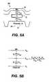
- FIG. 5Aillustrates a sectional perspective view of a memory transistor along the direction 5 A— 5 A shown in FIG. 2 and the equivalent capacitance between the charge storage unit and the word line and between the charge unit and the channel.
- FIG. 5Billustrates schematically the capacitive coupling of the memory transistor shown in FIG. 5A , showing in particular the voltage at the charge storage unit due to the voltage at the channel and the voltage at the word line.
- FIG. 6Aillustrates a sectional perspective view of the array of NAND cells shown in FIG. 3 for the case when two adjacent memory transistors are both in programming mode.
- FIG. 6Billustrates a sectional perspective view of the NAND array similar to FIG. 6A , except one of the adjacent memory transistors is in program inhibit mode.
- FIG. 7schematically represents the capacitive coupling between the two bit lines by a capacitor.
- FIGS. 8 (A)- 8 (G)are timing diagrams illustrating the voltage compensation scheme by capacitive bit line-bit line coupling during program operations, according to a first embodiment of the invention.
- FIGS. 8 (H)- 8 (O)illustrates the timing of the preferred sense module shown in FIG. 12 in relation to the features of the present invention.
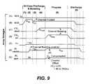
- FIGS. 9 (A)- 9 (G)are timing diagrams illustrating the voltage compensation scheme by capacitive bit line-bit line coupling during program operations, according to a second embodiment of the invention.
- FIG. 10is a flow diagram showing a method of programming a page of contiguous memory storage units while minimizing the coupling errors due to individual memory transistors among them being program inhibited or locked out, according to one preferred embodiment.
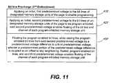
- FIG. 11is a flow diagram showing a method of programming a page of contiguous memory storage units while minimizing the coupling errors due to individual memory transistors among them being program inhibited or locked out, according to another preferred embodiment.
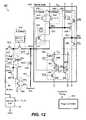
- FIG. 12illustrates a preferred sense module implementing the various aspects of the present invention.
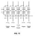
- FIG. 13illustrates a programming configuration along a row of NAND chains where a second order error may still occur.
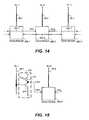
- FIG. 14illustrates a sense module configuration in which each sense module also senses the INV signal of its neighbors.
- FIG. 15illustrates an alternative implementation in which the signal indicating whether a neighbor is in program or program inhibit mode is derived directly from the state of the neighbor's bit line.
- the sense module 380 shown in FIG. 4A , FIG. 4 B and FIG. 12is preferably implemented in a memory architecture configured to perform all-bit-line sensing. In other words, contiguous memory cells in a row are each connectable to a sense module to perform sensing in parallel.
- a memory architectureis also disclosed in co-pending and commonly assigned U.S. patent application Ser. No. 10/254,483 filed by Cernea et al., on Sep. 24, 2002 entitled, “Highly Compact Non-Volatile Memory And Method Thereof.” The entire disclosure of said patent application is hereby incorporated herein by reference.
- the number of memory cells in a “page” that are programmed or read simultaneouslymay vary according to the size of data sent or requested by a host system.
- there are several ways to program the memory cells coupled to a single word linesuch as (1) programming even bit lines and odd bit lines separately, which may comprise upper page programming and lower page programming, (2) programming all the bit lines (“all-bit-line programming”), or (3) programming all the bit lines in a left or right page separately, which may comprise right page programming and a left page.
- FIG. 4Aillustrates schematically a memory device having read/write circuits for reading and programming a page of memory cells in parallel, according to one embodiment of the present invention.
- the memory deviceincludes a two-dimensional array of memory cells 300 , control circuitry 310 , and read/write circuits 370 .
- the memory array 300is addressable by word lines via a row decoder 330 and by bit lines via a column decoder 360 .
- the read/write circuits 370include multiple sense modules 380 and allow a page of memory cells to be read or programmed in parallel.
- the page of memory cells to be read or programmed in parallelis preferably a row of contiguous memory storage cells or storage units.
- the pageis a segment of a row of contiguous memory storage cells or storage units.
- the control circuitry 310cooperates with the read/write circuits 370 to perform memory operations on the memory array 300 .
- the control circuitry 310includes a state machine 312 , an on-chip address decoder 314 and a power control module 316 .
- the state machine 312provides chip level control of memory operations.
- the on-chip address decoder 314provides an address interface between that used by the host or a memory controller to the hardware address used by the decoders 330 and 370 .
- the power control module 316controls the power and voltages supplied to the word lines and bit lines during memory operations.
- FIG. 4Billustrates a preferred arrangement of the memory device shown in FIG. 4 A.
- Access to the memory array 300 by the various peripheral circuitsis implemented in a symmetric fashion, on opposite sides of the array so that the densities of access lines and circuitry on each side are reduced in half.
- the row decoderis split into row decoders 330 A and 330 B and the column decoder into column decoders 360 A and 360 B.
- the read/write circuitsare split into read/write circuits 370 A connecting to bit lines from the bottom and read/write circuits 370 B connecting to bit lines from the top of the array 300 . In this way, the density of the read/write modules, and therefore that of the sense modules 380 , is essentially reduced by one half.
- An error inherent in high-density integrated circuit, non-volatile memory deviceis due to the coupling of neighboring charge storage units and channel regions. If the channel region and charge storage unit of one memory storage unit is boosted relative to an adjacent one, it will cause a perturbation on the charge storage unit of the adjacent unit. This effect is more pronounced when the memory storage units being programmed in parallel are densely packed or inadequately shielded.
- FIG. 5Aillustrates a sectional perspective view of a memory transistor along the direction 5 A— 5 A shown in FIG. 2 and the equivalent capacitance between the charge storage unit and the word line and between the charge unit and the channel.
- the memory transistor M 1has the control gate 60 being formed as part of a word line running along a row of the NAND array 100 (see FIG. 3 ). In this view, the drain is coming out of the page of FIG. 5 A and the source is at the back, defining a channel region 80 in between.
- a charge storage unit 70is interposed between the control gate 60 and the channel 80 and is insulated from both of them by layers of dielectric material.
- the electrical coupling between the charge storage unit 70 and the control gate 60can be modeled by an equivalent capacitor C WF .
- the coupling between the charge storage unit 70 with the channel 80can be modeled by an equivalent capacitor C FC .
- FIG. 5Billustrates schematically the capacitive coupling of the memory transistor shown in FIG. 5A , showing in particular the voltage at the charge storage unit due to the voltage at the channel and the voltage at the word line.
- C WF and C FCboth hold the same charge.
- a memory transistorsuch as M 1 is placed in a program inhibit mode
- the channel voltageis boosted to a high voltage. Therefore this will also result in a boosted voltage at the charge storage unit.
- the combination of boosted voltages at the channel 80 and the charge storage unit 70will have a perturbation effect on adjacent memory transistors engaged in a programming mode.
- FIG. 6Aillustrates a sectional perspective view of the array of NAND cells shown in FIG. 3 for the case when two adjacent memory transistors are both in programming mode.
- FIG. 6Amay represent three adjacent memory transistors, such as M 1 - 1 , M 1 - 2 and M 1 - 3 respectively belonging to the NAND strings 50 - 1 , 50 - 2 and 50 - 3 , along a row sharing the same word line 60 .
- the NAND strings 50 - 1 , 50 - 2 and 50 - 3respectively have bit lines 36 - 1 , 36 - 2 and 36 - 3 connectable to them.
- the memory transistors M 1 - 1 , M 1 - 2 and M 1 - 3have corresponding charge storage units 70 - 1 , 70 - 2 and 70 - 3 and channels 80 - 1 , 80 - 2 and 80 - 3 .
- the memory transistorsWith increasing density of the memory array, the memory transistors are formed closer together and their effect on each other becomes more significant.
- the threshold voltage of the memory transistor M 1 - 2is dependent on the voltage on its charge storage unit 70 - 2 . Because of the close proximity to its adjacent neighbors M 1 - 1 and M 1 - 3 , the voltages at the channels and charge storage units of M 1 - 1 and M 1 - 3 can affect the voltage on the charge storage unit of M 1 - 2 .
- the charge storage unit 70 - 2may be regarded as coupled to its adjacent charge storage units 70 - 1 and 70 - 3 respectively by equivalent capacitors C 12 and C 23 .
- the charge storage unit 70 - 2may be regarded as coupled to its adjacent channels 80 - 1 and 80 - 3 respectively by equivalent capacitors C′ 12 and C′ 23 . The closer the spacing between the memory transistors, the more will the coupling be between them.
- FIG. 6Aillustrates the case when two adjacent memory transistors M 1 - 2 and M 1 - 1 are both in programming mode. Focusing on the effect on M 1 - 2 due to M 1 - 1 , there is little variation due to the word line and bit line voltages since they are the same for M 1 - 2 and M 1 - 1 . The channel voltages are also similar.
- the only variation seen by the charge storage unit 70 - 2is due to that of the charge storage unit 70 - 1 , which is mainly a function of the charge it is holding or its data representation. For example, the voltage on the charge storage units of M 1 - 1 and M 1 - 2 may be about 1 to 2V.
- the perturbation due to this type of perturbationis typically accounted for by allowing sufficient margin between two different memory states.
- FIG. 6Billustrates a sectional perspective view of the NAND array similar to FIG. 6A , except one of the adjacent memory transistors is in program inhibit mode.
- M 1 - 2is being programmed while M 1 - 1 is inhibited from further programming.
- the word line voltageremains the same for both but the voltage on the bit line 36 - 1 of M 1 - 1 has now changed to V DD , which is a predetermined system voltage, e.g., ⁇ 2.5V. This effectively turns off the select transistor S 2 (see FIG.
- the channel 80 - 1 of M 1 - 1can be boosted to 10V. Boosting up the channel voltage will effectively reduce the potential difference between the channel and the charge storage unit, thereby discouraging pulling electrons from the channel to the charge storage unit to effect programming.
- a boosted channelwill cause a boosted charge storage unit.
- the memory transistor M 1 - 1when the memory transistor M 1 - 1 is in program inhibit mode, it can results in a voltage boost at the channel 80 - 1 of about 10V and a voltage boost at the charge storage unit 70 - 1 from 2V to 8V. This can significantly perturb a neighboring memory transistor (e.g., M 1 - 2 ) to be programmed.
- the charge storage unit 70 - 2 of M 1 - 2may for example have its voltage boosted by ⁇ V 2 ⁇ 0.2V.
- the memory transistor's threshold voltageis programmed in steps of between 0.8V to about 0.1V or less, this will results in M 1 - 2 being erroneously programmed to a higher threshold value than expected.
- M 1 - 2due to M 1 - 1 .
- M 1 - 3is also in program inhibit mode, its boosted voltage will couple in similar manner to contribute to the boosting of the voltage on the charge storage unit 70 - 2 of M 1 - 2 .
- the perturbation on the charge storage unit 70 - 2 of M 1 - 2can be as high as 0.2V. To M 1 - 2 under programming, this effect is equivalent to the programming voltage on its control gate being increased by as high as 0.4V.
- the memory cellmay have its threshold window partitioned with a separation of about 0.3V and the programming pulse step is incremented by about 0.1V each time so that it typically takes more than one pulse to traverse each partition.
- a current programming pulse stepmay bring M 1 - 2 to just below the threshold region designating the desired programmed state.
- the current pulse stepmay program M 1 - 1 and M 1 - 3 to their final state so that they are locked out from further programming by entering into program inhibit mode.
- M 1 - 2is suddenly subjected to a large programming step of as much as 0.5V. This will likely make M 1 - 2 over shoot the desired threshold region and be programmed erroneously into the next memory state.
- FIG. 7illustrates the bit-line to bit-line coupling mechanism for compensating the perturbation from an adjacent memory transistor in program inhibit mode, according to a preferred embodiment of the present invention.
- the memory transistor M 1 - 2is being programmed while the adjacent M 1 - 1 is inhibited from further programming.
- the boosted channel 80 - 1 and charge storage unit 70 - 1 of M 1 - 1will result in the voltage at the charge storage unit 70 - 2 of M 1 - 2 boosted by ⁇ V 2 , thereby resulting in a programming error.
- the perturbing ⁇ V 2 at the charge storage unit 70 - 2is compensated by introducing a similar amount on the bit line 36 - 2 .
- This bit line compensated voltagewill be passed to the channel so that the net change in the potential difference between the charge storage unit 70 - 2 and the channel 80 - 2 will be effectively zero. In this way, any errors in the threshold voltage will be canceled out.
- An auto-compensating schemeis employed. Any time a memory transistor such as M 1 - 1 enters into a program inhibit mode, its bit line 36 - 1 changes from a voltage of 0V to V DD so that its channel can be enabled for floating to achieve program inhibited boosting. This rise in bit line voltage can be used to boost the voltage of a neighboring bit line such as the bit line 36 - 2 by capacitive coupling between the two bit lines.
- FIG. 7schematically represents the capacitive coupling between the two bit lines 36 - 1 and 36 - 2 by a capacitor C BL12 .
- a similar capacitor C BL23exists between the bit lines 36 - 2 and 36 - 3 .
- ⁇ V 1is a predetermined voltage such that the coupled portion ⁇ V 1 ⁇ V 2 .
- the bit line 36 - 1(for the program lockout or inhibited memory transistor M 1 - 1 ) changes from 0V to V DD
- the bit line 36 - 2(for the memory transistor M 1 - 2 to be programmed) is floated to couple in a predetermined ⁇ V 1 .
- the bit line 36 - 2is set to 0V (not floated) during a first period where the voltage of the bit line 36 - 1 rises from 0V to V DD ⁇ V 1 .
- bit line 36 - 1rises by the last ⁇ V 1
- bit line 36 - 2is floated to couple in ⁇ V 1 ⁇ V 2 .
- its bit line 36 - 2 voltageis compensated by an offset equal to ⁇ V 2 whenever one of its neighboring transistor (e.g., M 1 - 1 in NAND chain 50 - 1 ) enters into a program inhibit mode.
- FIGS. 8 (A)- 8 (G)are timing diagrams illustrating the voltage compensation scheme by capacitive bit line-bit line coupling during program operations, according to, a first embodiment of the invention.
- the voltages shownare applied to various word lines and bit lines of the memory array, for NAND chains under programming and program inhibition (see also FIG. 2 and FIG. 3 ).
- the program operationcan be grouped into a Bit Lines Precharge Phase, a Program Phase and a Discharge Phase.
- the source select transistoris turned off by SGS at 0V (FIG. 8 (A)) while the drain select transistor is turned on by SGD going high to V SG (FIG. 8 (B)), thereby allowing a bit line to access a NAND chain.
- bit line voltage of a program inhibited NAND chainis allowed to rise (in the first of a two-step rise) to a predetermined voltage given by V DD ⁇ V 1 (FIG. 8 (F)). At the same time, the bit line voltage of a programming NAND chain is actively pulled down to 0V (FIG. 8 (G)).
- the drain word line connecting to the drain select transistors of a row of NAND chainshas its voltage drop to V DD . This will only float those program inhibited NAND chains where their bit line voltage is comparable to V DD , since their drain select transistors are turned off (FIGS. 8 (B) & 8 (F)). As for the NAND chains containing a memory transistor to be programmed, their drain select transistors will not be turned off relative to the bit line voltage of near 0V at their drain. Also, as mentioned earlier, when a memory transistor to be programmed is next to one under program inhibition, its charge storage unit will have coupled in ⁇ V 2 due to the neighbor's boosted channel and charge storage unit.
- V PASSis typically set to some intermediate voltage (e.g. ⁇ 10V) relative to V PGM (e.g. ⁇ 15-24V).
- V PASShelps to reduce the effective V DS for the cell subjected to the higher voltage V PGM , thereby helping to reduce leakage.
- V PASSshould ideally be at ground potential, thus an intermediate V PASS voltage would be a reasonable compromise.
- the various control lines and bit linesare allowed to discharge.
- the firstis due to an adjacent memory transistor having a floated channel and charge storage unit capacitively boosted by a high control gate voltage from a word line. This occurs when a NAND chain is put into program inhibit mode.
- the first type of boosting due an adjacent program inhibit memory transistorboosts the voltage on a charge storage unit of the memory transistor to be programmed. This is an undesirable side effect of program inhibition.
- the secondis a compensatory adjustment on the bit line of the memory transistor to be programmed in order to offset the first boosting. By floating the bit line during some period when the voltage of a neighboring bit line is raised, the bit line acquires by capacitive coupling a boost in voltage to offset the effect of the first boosting.
- the second compensatory bit line boostingoccurs before the first boosting.
- Thisprovides a maximum range of possible ⁇ V 1 .
- the bit line of the memory transistor to be programmedwill become floated and it voltage susceptible to be moved by subsequent high programming voltages.
- the bit line capacitanceis considerably greater than the channel capacitance, and therefore, even if the bit line is floated, the bit line and channel voltage will not change much when a high programming voltage appears on the control gate.
- the first boostingis started first, followed by the second boosting. In this way, any coupling to the floated bit line due to high programming voltage is minimized.
- FIGS. 9 (A)- 9 (G)are timing diagrams illustrating the voltage compensation scheme by capacitive bit line-bit line coupling during program operations, according to a second embodiment of the invention.
- the source select transistoris turned off by SGS at 0V (FIG. 9 (A)) while the drain select transistor is turned on by SGD going high to V SG (FIG. 9 (B)), thereby allowing a bit line to access a NAND chain.
- bit line voltage of a program inhibited NAND chainis raised (in the first of a two-step rise) to a predetermined voltage given by V DD ⁇ V 1 (FIG. 9 (F)).
- This predetermined voltageis sufficient to cut off the drain of the NAND chain from its bit line when SGD drops to V DD in (3), thereby floating the channels therein.
- the bit line voltage of a programming NAND chainis fixed at 0V (FIG. 9 (G)).
- the memory transistors in a NAND chain not being addressedhave their control gate voltage set to V PASS to fully turn them on (FIG. 9 (C)). Since a program inhibited NAND chain is floating, the high V PASS and V PGM applied to the unaddressed memory transistors boosts up the voltages at their channels and charge storage elements, thereby inhibiting programming.
- bit line voltage of the program inhibited NAND chainchanges (in the second of a the two-step rise) by ⁇ V 1 in this period as it continue to rise to V DD (FIG. 9 (F)).
- Programming voltageis applied to the control gate of a memory transistor selected for programming (FIG. 9 (D)).
- the ones under program inhibitioni.e., with boosted channels and charge storage units
- FIG. 10is a flow diagram showing a method of programming a page of contiguous memory storage units while minimizing the coupling errors due to individual memory transistors among them being program inhibited or locked out, according to one preferred embodiment.
- STEP 400For a page of contiguous memory storage units, each unit having a charge storage unit between a control gate and a channel region defined by a source and a drain, providing a bit line switchably coupled to the drain of each unit and a word line coupled to all the control gates of said page of memory storage units.
- STEP 410Applying an initial, first predetermined voltage to the bit lines of designated memory storage units of the page to enable programming.
- STEP 420Applying an initial, second predetermined voltage to the bit lines of un-designated memory storage units of the page to be program inhibited.
- STEP 430Floating the program-enabled bit lines, while raising the program-inhibited bit lines from said second predetermined voltage by a predetermined voltage difference to a third predetermined voltage, wherein a predetermined portion of the predetermined voltage difference is coupled as an offset to any neighboring, floated, program-enabled bit lines, and said third predetermined voltage enables floating of the channel of each program-inhibited memory storage unit.
- STEP 440Applying a programming voltage pulse to the word line in order to program the designated memory storage units of the page, wherein those un-designated memory storage units of the page are program inhibited by virtue of their floated channel boosted to a program inhibited voltage condition, and a perturbation resulted from the boosting on any neighboring program-enabled memory storage units is compensated by said offset.
- STEP 450Verifying the selected memory storage units under programming.
- STEP 460Re-designating any memory storage units that have not been verified.
- STEP 470Are all memory storage units of the page verified? If not, return to STEP 420 . If so, proceed to STEP 480 .
- FIG. 11is a flow diagram showing a method of programming a page of contiguous memory storage units while minimizing the coupling errors due to individual memory transistors among them being program inhibited or locked out, according to another preferred embodiment. This embodiment is similar to that shown in FIG. 10 , except in the steps for Precharge with Perturb Offset, the boosting the channel step precedes the floating the bit line steps.
- STEP 410 ′Applying an initial, first predetermined voltage to the bit lines of designated memory storage units of the page to enable programming.
- STEP 420 ′Applying an initial, second predetermined voltage to the bit lines of un-designated memory storage units of the page to be program inhibited, said second predetermined voltage enables floating of the bit line and channel of each program-inhibited memory storage unit.
- STEP 430 ′Floating the program-enabled bit lines, while raising the program-inhibited bit lines from said second predetermined voltage by a predetermined voltage difference to a third predetermined voltage, wherein a predetermined portion of the predetermined voltage difference is coupled as an offset to any neighboring, floated, program-enabled bit lines, and said third predetermined voltage enables floating of the channel of each program-inhibited memory storage unit.
- FIG. 12illustrates a preferred sense module implementing the various aspects of the present invention.
- the sense module 380comprises a bit line isolation transistor 502 , a bit line pull down circuit 520 , a bit line voltage clamp 610 , a readout bus transfer gate 530 and a sense amplifier 600 .
- a page controller 540expediently provides control and timing signals to the sense modules operated in parallel.
- the sense module 380is connectable to the bit line 36 of a memory cell 10 when the bit line isolation transistor 502 is enabled by a signal BLS.
- the sense module 380senses the conduction current of the memory cell 10 by means of the sense amplifier 600 and latches the read result as a digital voltage level SEN 2 at a sense node 501 and outputs it to a readout bus 532 .
- the sense amplifier 600essentially comprises a second voltage clamp 620 , a precharge circuit 640 , a discriminator or compare circuit 650 and a latch 660 .
- the discriminator circuit 650includes a dedicated capacitor 652 .
- the bit line voltage levelis set to a level such that it is sufficiently low to avoid a long precharge time, yet sufficiently high to avoid ground noise and other factors.
- the sense amplifier 600senses the conduction current through the sense node 501 and determines whether the conduction current is above or below a predetermined value.
- the sense amplifieroutputs the sensed result in a digital form as the signal SEN 2 at the sense node 501 to the readout bus 532 .
- the digital control signal INVwhich is essentially an inverted state of the signal SEN 2 , is also output to control the pull down circuit 520 .
- the pull down circuit 520includes an n-transistor 522 controlled by the control signal INV and another n-transistor 550 controlled by the control signal GRS.
- the GRS signalbasically allows the bit line 36 to be floated when its goes LOW regardless of the state of the INV signal. During programming, the GRS signal goes HIGH to allow the bit line 36 to be pulled to ground. When the bit line is required to be floated, the GRS signal goes LOW.
- FIGS. 8 (H)- 8 (O)illustrates the timing of the preferred sense module shown in FIG. 12 in relation to the features of the present invention.
- Detailed description of the operation of the preferred sense module in regards to other inventive featureshas been described and claimed in co-pending and co-owned U.S. patent application Ser. No., 10/254,830 filed on Sep. 24, 2002 by Adrian-Raul Cernea and Yan Li. The entire disclosure of the referenced application is hereby incorporated herein by reference.
- NAND chains on the same set of word lines that no longer need programmingthey are program inhibited or locked out in spite of being subjected to programming voltages on their control gates. This is accomplished by reducing the tunneling potential.
- the NAND chain to be program inhibithas its bit line raised from ground to V DD . This effectively turns off the drain select transistor and floats the channel of the NAND chain. As the channel is floated, it will rise from ground to a higher voltage because of the high programming voltages appear on the word lines. This reduces the tunneling potential between the associated floating gate and the channel to inhibit programming.
- a gross schemeis to ground the channel of a NAND chain to create a favorable condition for programming and to float the channel for inhibiting programming.
- a NAND chain under programmingis perturbed by the high potential on the channel of one or both of its neighbors if they are in program inhibit mode.
- the scheme described earliercompensates this perturbation by attempting to adjust the bit line voltage of the NAND chain under programming by the same amount in a sort of “common-mode” cancellation.
- the adjustmentis accomplished by floating the bit line from ground and capacitively coupling a portion of the neighboring bit line voltage when it transits from zero to V DD .
- FIG. 13illustrates a programming configuration along a row of NAND chains where a second order error may still occur. This occurs when a NAND chain 50 under programming is flanked by two adjacent chains 51 , 51 ′ also under programming and further flanked by two next-to-adjacent chains 52 , 52 ′ that are in program inhibit mode.
- the scheme described abovecalls for the chains under programming 50 , 51 , and 5 ′ to have their bit lines 36 - 0 , 36 - 1 , 36 - 1 ′ floated and capacitively coupled from ground a voltage from their neighboring bit lines.
- the bit line coupled to the NAND chainis forced to a voltage so as to maximize the potential difference between the cell's floating gate and channel. In a preferred embodiment, this would require the bit line to be set to ground potential. This will require the NAND chain to be cognizant of the state of its neighbors, i.e., whether they are in program or program inhibit modes.
- a sense modulesuch as the sense module 380 shown in FIG. 12 controls the voltage on the bit line.
- the sense module 380 and in particular the sense amplifier 600 coupled to the bit line 36generates a control signal INV that is HIGH when in program mode and LOW when in program inhibit mode.
- the signal INVcan be used to indicate to a neighbor whether the NAND chain coupled to the bit line 36 is in program or program inhibit mode.
- FIG. 14illustrates a sense module configuration in which each sense module also senses the INV signal of its neighbors.
- the bit line 36 - 0is flanked by the bit lines 36 - 1 and 36 - 1 ′ respectively.
- the sense module 380 - 0is coupled to the bit line 36 - 0 and the sense modules 380 - 1 and 380 - 1 ′ are respectively coupled to the bit line 36 - 1 and 36 - 1 ′. Since each sense module receives the INV signals from its adjacent neighbors, the sense module 380 - 0 receives the INV signal from the sense module 380 - 1 and 380 - 1 ′ respectively as input signals INV L and INV R . Similarly the INV signal of the sense module 380 - 0 is input to the sense modules 380 - 1 and 380 - 1 ′′.
- FIG. 12illustrates a sense module responsive to the neighboring states for pulling down the bit line to ground, according a preferred embodiment.
- Thisis implemented by an optional bit line pull-down circuit 560 for pulling down the node 523 to ground depending on the neighboring states.
- INVWhen the NAND chain coupled to the bit line 36 is in program mode, INV is HIGH, and the transistor 522 is conducting so that the bit line is coupled to the node 523 .
- the bit line pull-down circuitincludes two n-transistors connected in series to ground. The conduction of the two n-transistors are controlled by the INV signals INV L and INV R input from the neighboring sense modules 380 ′ and 380 ′′ respectively.
- both INV L and INV RWhen both neighbors are in program mode, both INV L and INV R will also be HIGH, thereby pulling the node 523 and therefore the bit line 36 to ground. Conversely, if one or more of the neighbors are in program inhibit mode, the node 523 will not be pulled to ground by the circuit 560 .
- FIG. 15illustrates an alternative implementation in which the signal indicating whether a neighbor is in program or program inhibit mode is derived directly from the state of the neighbor's bit line. This scheme is useful when the signal is not readily available from a neighboring sense module. As described earlier, when a NAND chain is in program mode, its bit line voltage is kept around ground potential and when it is in program inhibit mode, its bit line voltage is kept at V DD .
- a virtual INV signal generator 570senses the bit line voltage and outputs a virtual INV signal, VINV, which is logically equivalent to the INV signal generated by a sense module.
- the virtual INV signal generator 570comprises a p-transistor 572 in series with an n-transistor 574 in a pull up/down configuration for the node that outputs the signal VINV.
- the p-transistor 572is weakly pulled up by a voltage V WKP at its gate.
- the voltage of the bit line 36 ′is input to the gate of the n-transistor 574 .
- the virtual INV signal generator 570essentially behaves like a tri-state inverter that outputs a HIGH VINV signal when the bit line 36 - 1 has a voltage close to ground (program mode) and outputs a LOW VINV signal when the voltage is at V DD (program inhibit mode.)
- the VINV signalis input as the signal VINV L to the neighboring sense module 380 - 0 .
- the sense module 380 - 0uses either the signal INV or VINV, information about the programming or program inhibiting state is communicated to the sense module 380 - 0 coupled to a NAND chain.
- the sense module 380 - 0pulls down the bit line to ground by way of the bit line pull-down circuit 560 .
Landscapes
- Engineering & Computer Science (AREA)
- Microelectronics & Electronic Packaging (AREA)
- Computer Hardware Design (AREA)
- Read Only Memory (AREA)
- Semiconductor Memories (AREA)
- Non-Volatile Memory (AREA)
- Techniques For Improving Reliability Of Storages (AREA)
Abstract
Description
Claims (30)
Priority Applications (11)
| Application Number | Priority Date | Filing Date | Title |
|---|---|---|---|
| US10/667,222US7064980B2 (en) | 2003-09-17 | 2003-09-17 | Non-volatile memory and method with bit line coupled compensation |
| JP2006526937AJP4658052B2 (en) | 2003-09-17 | 2004-09-08 | Nonvolatile memory and method with coupling compensation between bitlines |
| PCT/US2004/029426WO2005029502A1 (en) | 2003-09-17 | 2004-09-08 | Non-volatile memory and method with bit line to bit line coupled compensation |
| EP04783607AEP1671332B1 (en) | 2003-09-17 | 2004-09-08 | Non-volatile memory and method with bit line to bit line coupled compensation |
| AT04783607TATE433597T1 (en) | 2003-09-17 | 2004-09-08 | NON-VOLATILE MEMORY AND METHOD WITH BIT-LINE-TO-BIT-LINE COUPLED COMPENSATION |
| CNB2004800329386ACN100538906C (en) | 2003-09-17 | 2004-09-08 | Nonvolatile memory and method with bit line coupled compensation |
| DE602004021493TDE602004021493D1 (en) | 2003-09-17 | 2004-09-08 | NON-VOLATILE MEMORY AND METHOD WITH COMPONENT COUPLED BY BIT LINE TO BIT LINE |
| TW093128297ATWI295803B (en) | 2003-09-17 | 2004-09-17 | Non-volatile memory and method with bit line to bit line coupled compensation |
| KR1020067005471AKR101076239B1 (en) | 2003-09-17 | 2006-03-17 | Non-volatile memory and method with bit-to-bit connection compensation |
| US11/422,034US7269069B2 (en) | 2003-09-17 | 2006-06-02 | Non-volatile memory and method with bit line to bit line coupled compensation |
| US11/848,385US7532514B2 (en) | 2003-09-17 | 2007-08-31 | Non-volatile memory and method with bit line to bit line coupled compensation |
Applications Claiming Priority (1)
| Application Number | Priority Date | Filing Date | Title |
|---|---|---|---|
| US10/667,222US7064980B2 (en) | 2003-09-17 | 2003-09-17 | Non-volatile memory and method with bit line coupled compensation |
Related Child Applications (1)
| Application Number | Title | Priority Date | Filing Date |
|---|---|---|---|
| US11/422,034ContinuationUS7269069B2 (en) | 2003-09-17 | 2006-06-02 | Non-volatile memory and method with bit line to bit line coupled compensation |
Publications (2)
| Publication Number | Publication Date |
|---|---|
| US20050057965A1 US20050057965A1 (en) | 2005-03-17 |
| US7064980B2true US7064980B2 (en) | 2006-06-20 |
Family
ID=34274757
Family Applications (3)
| Application Number | Title | Priority Date | Filing Date |
|---|---|---|---|
| US10/667,222Expired - LifetimeUS7064980B2 (en) | 2003-09-17 | 2003-09-17 | Non-volatile memory and method with bit line coupled compensation |
| US11/422,034Expired - LifetimeUS7269069B2 (en) | 2003-09-17 | 2006-06-02 | Non-volatile memory and method with bit line to bit line coupled compensation |
| US11/848,385Expired - LifetimeUS7532514B2 (en) | 2003-09-17 | 2007-08-31 | Non-volatile memory and method with bit line to bit line coupled compensation |
Family Applications After (2)
| Application Number | Title | Priority Date | Filing Date |
|---|---|---|---|
| US11/422,034Expired - LifetimeUS7269069B2 (en) | 2003-09-17 | 2006-06-02 | Non-volatile memory and method with bit line to bit line coupled compensation |
| US11/848,385Expired - LifetimeUS7532514B2 (en) | 2003-09-17 | 2007-08-31 | Non-volatile memory and method with bit line to bit line coupled compensation |
Country Status (9)
| Country | Link |
|---|---|
| US (3) | US7064980B2 (en) |
| EP (1) | EP1671332B1 (en) |
| JP (1) | JP4658052B2 (en) |
| KR (1) | KR101076239B1 (en) |
| CN (1) | CN100538906C (en) |
| AT (1) | ATE433597T1 (en) |
| DE (1) | DE602004021493D1 (en) |
| TW (1) | TWI295803B (en) |
| WO (1) | WO2005029502A1 (en) |
Cited By (30)
| Publication number | Priority date | Publication date | Assignee | Title |
|---|---|---|---|---|
| US20040057318A1 (en)* | 2002-09-24 | 2004-03-25 | Sandisk Corporation | Non-volatile memory and method with reduced bit line crosstalk errors |
| US20060158947A1 (en)* | 2002-09-24 | 2006-07-20 | Chan Siu L | Reference sense amplifier for non-volatile memory |
| US20060158935A1 (en)* | 2002-09-24 | 2006-07-20 | Chan Siu L | Method for compensated sensing in non-volatile memory |
| US20060203545A1 (en)* | 2002-09-24 | 2006-09-14 | Raul-Adrian Cernea | Memory Sensing Circuit and Method for Low Voltage Operation |
| US20060209592A1 (en)* | 2005-03-16 | 2006-09-21 | Yan Li | Non-volatile memory and method with power-saving read and program-verify operations |
| US20060227614A1 (en)* | 2003-09-17 | 2006-10-12 | Raul-Adrian Cernea | Non-Volatile Memory and Method With Bit Line to Bit Line Coupled Compensation |
| US20070109847A1 (en)* | 2002-09-24 | 2007-05-17 | Raul-Adrian Cernea | Non-Volatile Memory and Method With Improved Sensing |
| US20080019175A1 (en)* | 2006-07-20 | 2008-01-24 | Yan Li | System that compensates for coupling based on sensing a neighbor using coupling |
| US20080019173A1 (en)* | 2006-07-20 | 2008-01-24 | Yan Li | System for configuring compensation |
| US20080019185A1 (en)* | 2006-07-20 | 2008-01-24 | Yan Li | Compensating for coupling during programming |
| US20080019174A1 (en)* | 2006-07-20 | 2008-01-24 | Yan Li | Method for configuring compensation |
| US20080019193A1 (en)* | 2006-07-20 | 2008-01-24 | Yan Li | Compensating for coupling based on sensing a neighbor using coupling |
| US20080019186A1 (en)* | 2006-07-20 | 2008-01-24 | Yan Li | System that compensates for coupling during programming |
| US20080068891A1 (en)* | 2004-05-05 | 2008-03-20 | Guterman Daniel C | Boosting to control programming of non-volatile memory |
| US20080192550A1 (en)* | 2007-02-13 | 2008-08-14 | Micron Technology, Inc. | Circuits, systems and methods for driving high and low voltages on bit lines in non-volatile memory |
| US20090059660A1 (en)* | 2007-09-04 | 2009-03-05 | Dana Lee | Reducing the impact of interference during programming |
| US20090290429A1 (en)* | 2008-05-23 | 2009-11-26 | Yingda Dong | Enhanced bit-line pre-charge scheme for increasing channel boosting in non-volatile storage |
| US20100091576A1 (en)* | 2008-10-13 | 2010-04-15 | Samsung Electronics Co., Ltd. | Nonvolatile memory device, program method and precharge voltage boosting method thereof, and memory system including the nonvolatile memory device |
| US20100110795A1 (en)* | 2008-10-31 | 2010-05-06 | Satoru Tamada | Boosting seed voltage for a memory device |
| US20110063919A1 (en)* | 2009-09-14 | 2011-03-17 | Micron Technology, Inc. | Memory kink checking |
| US20110122702A1 (en)* | 2009-11-24 | 2011-05-26 | Yan Li | Programming memory with sensing-based bit line compensation to reduce channel-to-floating gate coupling |
| US20110122703A1 (en)* | 2009-11-24 | 2011-05-26 | Yan Li | Programming memory with direct bit line driving to reduce channel-to-floating gate coupling |
| US20110122695A1 (en)* | 2009-11-24 | 2011-05-26 | Yan Li | Programming memory with bit line floating to reduce channel-to-floating gate coupling |
| US20110134701A1 (en)* | 2009-12-04 | 2011-06-09 | Micron Technology, Inc. | Memory kink compensation |
| US8208310B2 (en) | 2010-05-04 | 2012-06-26 | Sandisk Technologies Inc. | Mitigating channel coupling effects during sensing of non-volatile storage elements |
| US8218366B2 (en) | 2010-04-18 | 2012-07-10 | Sandisk Technologies Inc. | Programming non-volatile storage including reducing impact from other memory cells |
| US8395936B2 (en) | 2011-05-09 | 2013-03-12 | Sandisk Technologies Inc. | Using channel-to-channel coupling to compensate floating gate-to-floating gate coupling in programming of non-volatile memory |
| US9146824B1 (en) | 2011-11-04 | 2015-09-29 | Marvell International Ltd. | Management of bit line errors based on a stored set of data |
| US9978457B1 (en)* | 2016-11-22 | 2018-05-22 | Macronix International Co., Ltd. | Method for operating memory array |
| US10580501B2 (en)* | 2018-05-14 | 2020-03-03 | Toshiba Memory Corporation | Semiconductor memory device |
Families Citing this family (110)
| Publication number | Priority date | Publication date | Assignee | Title |
|---|---|---|---|---|
| US6987693B2 (en)* | 2002-09-24 | 2006-01-17 | Sandisk Corporation | Non-volatile memory and method with reduced neighboring field errors |
| KR100615975B1 (en) | 2002-09-24 | 2006-08-28 | 쌘디스크 코포레이션 | Non-volatile memory and its sensing method |
| US6956770B2 (en) | 2003-09-17 | 2005-10-18 | Sandisk Corporation | Non-volatile memory and method with bit line compensation dependent on neighboring operating modes |
| US7020026B2 (en)* | 2004-05-05 | 2006-03-28 | Sandisk Corporation | Bitline governed approach for program control of non-volatile memory |
| US7193898B2 (en)* | 2005-06-20 | 2007-03-20 | Sandisk Corporation | Compensation currents in non-volatile memory read operations |
| US7206235B1 (en) | 2005-10-14 | 2007-04-17 | Sandisk Corporation | Apparatus for controlled programming of non-volatile memory exhibiting bit line coupling |
| US7286406B2 (en)* | 2005-10-14 | 2007-10-23 | Sandisk Corporation | Method for controlled programming of non-volatile memory exhibiting bit line coupling |
| WO2007132456A2 (en) | 2006-05-12 | 2007-11-22 | Anobit Technologies Ltd. | Memory device with adaptive capacity |
| WO2007132453A2 (en) | 2006-05-12 | 2007-11-22 | Anobit Technologies Ltd. | Distortion estimation and cancellation in memory devices |
| KR101202537B1 (en) | 2006-05-12 | 2012-11-19 | 애플 인크. | Combined distortion estimation and error correction coding for memory devices |
| ATE522905T1 (en)* | 2006-07-20 | 2011-09-15 | Sandisk Corp | COMPENSATION FOR COUPLING BETWEEN ADJACENT MEMORY ELEMENTS IN A NON-VOLATILE MEMORY BASED ON SENSING A NEIGHBOR WITH COUPLING |
| US7894269B2 (en)* | 2006-07-20 | 2011-02-22 | Sandisk Corporation | Nonvolatile memory and method for compensating during programming for perturbing charges of neighboring cells |
| WO2008011441A2 (en)* | 2006-07-20 | 2008-01-24 | Sandisk Corporation | Method for configuring compensation for coupling between adjacent storage elements in a nonvolatile memory |
| KR101048834B1 (en) | 2006-07-20 | 2011-07-13 | 샌디스크 코포레이션 | Coupling Compensation During Programming |
| EP1883076B1 (en)* | 2006-07-28 | 2011-12-21 | STMicroelectronics Srl | Method of programming cells of a NAND memory device |
| WO2008026203A2 (en)* | 2006-08-27 | 2008-03-06 | Anobit Technologies | Estimation of non-linear distortion in memory devices |
| US7710786B2 (en) | 2006-08-28 | 2010-05-04 | Micron Technology, Inc. | NAND flash memory programming |
| JP2008090451A (en)* | 2006-09-29 | 2008-04-17 | Toshiba Corp | Storage device |
| KR100773742B1 (en)* | 2006-09-30 | 2007-11-09 | 삼성전자주식회사 | Non-volatile memory device and method for reducing coupling effect between storage elements |
| US7975192B2 (en) | 2006-10-30 | 2011-07-05 | Anobit Technologies Ltd. | Reading memory cells using multiple thresholds |
| WO2008068747A2 (en) | 2006-12-03 | 2008-06-12 | Anobit Technologies Ltd. | Automatic defect management in memory devices |
| KR100845135B1 (en) | 2006-12-22 | 2008-07-09 | 삼성전자주식회사 | A program method in a nonvolatile memory device and a nonvolatile memory device therefor |
| US8151166B2 (en) | 2007-01-24 | 2012-04-03 | Anobit Technologies Ltd. | Reduction of back pattern dependency effects in memory devices |
| US7660166B2 (en)* | 2007-01-31 | 2010-02-09 | Sandisk Il Ltd. | Method of improving programming precision in flash memory |
| US8369141B2 (en) | 2007-03-12 | 2013-02-05 | Apple Inc. | Adaptive estimation of memory cell read thresholds |
| US8001320B2 (en) | 2007-04-22 | 2011-08-16 | Anobit Technologies Ltd. | Command interface for memory devices |
| US8234545B2 (en) | 2007-05-12 | 2012-07-31 | Apple Inc. | Data storage with incremental redundancy |
| WO2008139441A2 (en) | 2007-05-12 | 2008-11-20 | Anobit Technologies Ltd. | Memory device with internal signal processing unit |
| US7508715B2 (en)* | 2007-07-03 | 2009-03-24 | Sandisk Corporation | Coarse/fine program verification in non-volatile memory using different reference levels for improved sensing |
| US7599224B2 (en)* | 2007-07-03 | 2009-10-06 | Sandisk Corporation | Systems for coarse/fine program verification in non-volatile memory using different reference levels for improved sensing |
| CN101350221B (en)* | 2007-07-20 | 2010-12-15 | 中芯国际集成电路制造(上海)有限公司 | Method for preventing non-volatility memory array from generating bit line interference |
| US8259497B2 (en) | 2007-08-06 | 2012-09-04 | Apple Inc. | Programming schemes for multi-level analog memory cells |
| US7652929B2 (en)* | 2007-09-17 | 2010-01-26 | Sandisk Corporation | Non-volatile memory and method for biasing adjacent word line for verify during programming |
| US8174905B2 (en) | 2007-09-19 | 2012-05-08 | Anobit Technologies Ltd. | Programming orders for reducing distortion in arrays of multi-level analog memory cells |
| US8000141B1 (en) | 2007-10-19 | 2011-08-16 | Anobit Technologies Ltd. | Compensation for voltage drifts in analog memory cells |
| US8068360B2 (en) | 2007-10-19 | 2011-11-29 | Anobit Technologies Ltd. | Reading analog memory cells using built-in multi-threshold commands |
| US8527819B2 (en) | 2007-10-19 | 2013-09-03 | Apple Inc. | Data storage in analog memory cell arrays having erase failures |
| US7916551B2 (en) | 2007-11-06 | 2011-03-29 | Macronix International Co., Ltd. | Method of programming cell in memory and memory apparatus utilizing the method |
| US8270246B2 (en) | 2007-11-13 | 2012-09-18 | Apple Inc. | Optimized selection of memory chips in multi-chips memory devices |
| US8225181B2 (en) | 2007-11-30 | 2012-07-17 | Apple Inc. | Efficient re-read operations from memory devices |
| US8209588B2 (en) | 2007-12-12 | 2012-06-26 | Anobit Technologies Ltd. | Efficient interference cancellation in analog memory cell arrays |
| US8085586B2 (en) | 2007-12-27 | 2011-12-27 | Anobit Technologies Ltd. | Wear level estimation in analog memory cells |
| US8156398B2 (en) | 2008-02-05 | 2012-04-10 | Anobit Technologies Ltd. | Parameter estimation based on error correction code parity check equations |
| JP4640658B2 (en)* | 2008-02-15 | 2011-03-02 | マイクロン テクノロジー, インク. | Multi-level suppression scheme |
| US8230300B2 (en) | 2008-03-07 | 2012-07-24 | Apple Inc. | Efficient readout from analog memory cells using data compression |
| US8400858B2 (en) | 2008-03-18 | 2013-03-19 | Apple Inc. | Memory device with reduced sense time readout |
| US8059457B2 (en) | 2008-03-18 | 2011-11-15 | Anobit Technologies Ltd. | Memory device with multiple-accuracy read commands |
| US8498151B1 (en) | 2008-08-05 | 2013-07-30 | Apple Inc. | Data storage in analog memory cells using modified pass voltages |
| US8949684B1 (en) | 2008-09-02 | 2015-02-03 | Apple Inc. | Segmented data storage |
| US8169825B1 (en) | 2008-09-02 | 2012-05-01 | Anobit Technologies Ltd. | Reliable data storage in analog memory cells subjected to long retention periods |
| US8482978B1 (en) | 2008-09-14 | 2013-07-09 | Apple Inc. | Estimation of memory cell read thresholds by sampling inside programming level distribution intervals |
| US8000135B1 (en) | 2008-09-14 | 2011-08-16 | Anobit Technologies Ltd. | Estimation of memory cell read thresholds by sampling inside programming level distribution intervals |
| US8239734B1 (en) | 2008-10-15 | 2012-08-07 | Apple Inc. | Efficient data storage in storage device arrays |
| US8713330B1 (en) | 2008-10-30 | 2014-04-29 | Apple Inc. | Data scrambling in memory devices |
| US8208304B2 (en) | 2008-11-16 | 2012-06-26 | Anobit Technologies Ltd. | Storage at M bits/cell density in N bits/cell analog memory cell devices, M>N |
| US8248831B2 (en) | 2008-12-31 | 2012-08-21 | Apple Inc. | Rejuvenation of analog memory cells |
| US8174857B1 (en) | 2008-12-31 | 2012-05-08 | Anobit Technologies Ltd. | Efficient readout schemes for analog memory cell devices using multiple read threshold sets |
| US8924661B1 (en) | 2009-01-18 | 2014-12-30 | Apple Inc. | Memory system including a controller and processors associated with memory devices |
| KR101016078B1 (en)* | 2009-01-21 | 2011-02-17 | 주식회사 하이닉스반도체 | Nonvolatile Memory Device and Its Operation Method |
| US8228701B2 (en) | 2009-03-01 | 2012-07-24 | Apple Inc. | Selective activation of programming schemes in analog memory cell arrays |
| US8259506B1 (en) | 2009-03-25 | 2012-09-04 | Apple Inc. | Database of memory read thresholds |
| US8832354B2 (en) | 2009-03-25 | 2014-09-09 | Apple Inc. | Use of host system resources by memory controller |
| US8238157B1 (en) | 2009-04-12 | 2012-08-07 | Apple Inc. | Selective re-programming of analog memory cells |
| US8479080B1 (en) | 2009-07-12 | 2013-07-02 | Apple Inc. | Adaptive over-provisioning in memory systems |
| US8081514B2 (en)* | 2009-08-25 | 2011-12-20 | Sandisk Technologies Inc. | Partial speed and full speed programming for non-volatile memory using floating bit lines |
| US8619474B2 (en)* | 2009-09-10 | 2013-12-31 | Micron Technology, Inc. | Data line management in a memory device |
| US8495465B1 (en) | 2009-10-15 | 2013-07-23 | Apple Inc. | Error correction coding over multiple memory pages |
| US8677054B1 (en) | 2009-12-16 | 2014-03-18 | Apple Inc. | Memory management schemes for non-volatile memory devices |
| US8694814B1 (en) | 2010-01-10 | 2014-04-08 | Apple Inc. | Reuse of host hibernation storage space by memory controller |
| US8572311B1 (en) | 2010-01-11 | 2013-10-29 | Apple Inc. | Redundant data storage in multi-die memory systems |
| KR101691092B1 (en) | 2010-08-26 | 2016-12-30 | 삼성전자주식회사 | Nonvolatile memory device, operating method thereof and memory system including the same |
| KR101691088B1 (en) | 2010-02-17 | 2016-12-29 | 삼성전자주식회사 | Nonvolatile memory device, operating method thereof and memory system including the same |
| KR101658479B1 (en) | 2010-02-09 | 2016-09-21 | 삼성전자주식회사 | Nonvolatile memory device, operating method thereof and memory system including the same |
| US9324440B2 (en) | 2010-02-09 | 2016-04-26 | Samsung Electronics Co., Ltd. | Nonvolatile memory devices, operating methods thereof and memory systems including the same |
| US9378831B2 (en) | 2010-02-09 | 2016-06-28 | Samsung Electronics Co., Ltd. | Nonvolatile memory devices, operating methods thereof and memory systems including the same |
| JP5788183B2 (en) | 2010-02-17 | 2015-09-30 | 三星電子株式会社Samsung Electronics Co.,Ltd. | Nonvolatile memory device, method of operating the same, and memory system including the same |
| US8908431B2 (en) | 2010-02-17 | 2014-12-09 | Samsung Electronics Co., Ltd. | Control method of nonvolatile memory device |
| US8923060B2 (en) | 2010-02-17 | 2014-12-30 | Samsung Electronics Co., Ltd. | Nonvolatile memory devices and operating methods thereof |
| JP2011170956A (en) | 2010-02-18 | 2011-09-01 | Samsung Electronics Co Ltd | Nonvolatile memory device, programming method thereof and memory system including the same |
| US8767487B2 (en)* | 2010-03-02 | 2014-07-01 | Micron Technology, Inc. | Drain select gate voltage management |
| US8792282B2 (en) | 2010-03-04 | 2014-07-29 | Samsung Electronics Co., Ltd. | Nonvolatile memory devices, memory systems and computing systems |
| US8553466B2 (en)* | 2010-03-04 | 2013-10-08 | Samsung Electronics Co., Ltd. | Non-volatile memory device, erasing method thereof, and memory system including the same |
| US8694853B1 (en) | 2010-05-04 | 2014-04-08 | Apple Inc. | Read commands for reading interfering memory cells |
| US8572423B1 (en) | 2010-06-22 | 2013-10-29 | Apple Inc. | Reducing peak current in memory systems |
| US8595591B1 (en) | 2010-07-11 | 2013-11-26 | Apple Inc. | Interference-aware assignment of programming levels in analog memory cells |
| KR101642015B1 (en) | 2010-07-23 | 2016-07-22 | 삼성전자주식회사 | Flash memory device and program method thereof |
| US9104580B1 (en) | 2010-07-27 | 2015-08-11 | Apple Inc. | Cache memory for hybrid disk drives |
| US8645794B1 (en) | 2010-07-31 | 2014-02-04 | Apple Inc. | Data storage in analog memory cells using a non-integer number of bits per cell |
| US8856475B1 (en) | 2010-08-01 | 2014-10-07 | Apple Inc. | Efficient selection of memory blocks for compaction |
| US8694854B1 (en) | 2010-08-17 | 2014-04-08 | Apple Inc. | Read threshold setting based on soft readout statistics |
| US9021181B1 (en) | 2010-09-27 | 2015-04-28 | Apple Inc. | Memory management for unifying memory cell conditions by using maximum time intervals |
| US8385132B2 (en) | 2010-12-22 | 2013-02-26 | Sandisk Technologies Inc. | Alternate bit line bias during programming to reduce channel to floating gate coupling in memory |
| KR101762828B1 (en) | 2011-04-05 | 2017-07-31 | 삼성전자주식회사 | Nonvolatile memory device and operating method of nonvolatile memory device |
| EP2754291A4 (en)* | 2011-09-06 | 2015-04-29 | Intel Corp | Analytics assisted encoding |
| KR101847095B1 (en)* | 2011-10-18 | 2018-04-10 | 에스케이하이닉스 주식회사 | Non-volatile memory device |
| US8988942B2 (en) | 2012-07-02 | 2015-03-24 | Sandisk Technologies Inc. | Methods for extending the effective voltage window of a memory cell |
| US9087601B2 (en) | 2012-12-06 | 2015-07-21 | Sandisk Technologies Inc. | Select gate bias during program of non-volatile storage |
| JP2014164773A (en)* | 2013-02-21 | 2014-09-08 | Toshiba Corp | Nonvolatile semiconductor memory device |
| KR102242022B1 (en) | 2013-09-16 | 2021-04-21 | 삼성전자주식회사 | Nonvolatile memory device and program method using thereof |
| JP6470146B2 (en) | 2015-08-27 | 2019-02-13 | 東芝メモリ株式会社 | Semiconductor memory device |
| KR102323612B1 (en)* | 2015-11-23 | 2021-11-08 | 에스케이하이닉스 주식회사 | Semiconductor memory device and operating method thereof |
| JP2017111847A (en) | 2015-12-17 | 2017-06-22 | 株式会社東芝 | Semiconductor memory device |
| KR102572610B1 (en)* | 2016-05-17 | 2023-09-01 | 에스케이하이닉스 주식회사 | Semiconductor memory device and operating method thereof |
| CN108962326B (en)* | 2017-05-25 | 2021-03-05 | 旺宏电子股份有限公司 | Sense amplifier and method for bit line voltage compensation thereof |
| US10839915B1 (en)* | 2019-06-27 | 2020-11-17 | Sandisk Technologies Llc | Bitline boost for nonvolatile memory |
| KR102771883B1 (en) | 2019-07-22 | 2025-02-21 | 삼성전자주식회사 | Non-volatile memory device and method for programming the device |
| US11393535B2 (en)* | 2020-02-26 | 2022-07-19 | Silicon Storage Technology, Inc. | Ultra-precise tuning of analog neural memory cells in a deep learning artificial neural network |
| KR20220015245A (en)* | 2020-07-30 | 2022-02-08 | 삼성전자주식회사 | Two way precharge during programming in non-volatile memory device |
| US11556416B2 (en) | 2021-05-05 | 2023-01-17 | Apple Inc. | Controlling memory readout reliability and throughput by adjusting distance between read thresholds |
| US11847342B2 (en) | 2021-07-28 | 2023-12-19 | Apple Inc. | Efficient transfer of hard data and confidence levels in reading a nonvolatile memory |
Citations (45)
| Publication number | Priority date | Publication date | Assignee | Title |
|---|---|---|---|---|
| US4357685A (en) | 1979-09-28 | 1982-11-02 | Sgs-Ates Componenti Elettronici S.P.A. | Method of programming an electrically alterable nonvolatile memory |
| US4785427A (en) | 1987-01-28 | 1988-11-15 | Cypress Semiconductor Corporation | Differential bit line clamp |
| US5070032A (en) | 1989-03-15 | 1991-12-03 | Sundisk Corporation | Method of making dense flash eeprom semiconductor memory structures |
| US5093806A (en) | 1988-02-16 | 1992-03-03 | Tran Hiep V | Sensing and decoding scheme for a bicmos read/write memory |
| US5095344A (en) | 1988-06-08 | 1992-03-10 | Eliyahou Harari | Highly compact eprom and flash eeprom devices |
| US5172338A (en) | 1989-04-13 | 1992-12-15 | Sundisk Corporation | Multi-state EEprom read and write circuits and techniques |
| US5245571A (en) | 1990-11-30 | 1993-09-14 | Nec Corporation | Sense amplifier circuit implemented by bipolar transistor and improved in current consumption |
| US5313421A (en) | 1992-01-14 | 1994-05-17 | Sundisk Corporation | EEPROM with split gate source side injection |
| US5315541A (en) | 1992-07-24 | 1994-05-24 | Sundisk Corporation | Segmented column memory array |
| US5343063A (en) | 1990-12-18 | 1994-08-30 | Sundisk Corporation | Dense vertical programmable read only memory cell structure and processes for making them |
| US5418752A (en) | 1989-04-13 | 1995-05-23 | Sundisk Corporation | Flash EEPROM system with erase sector select |
| US5537356A (en) | 1991-12-27 | 1996-07-16 | Fujitsu Limited | Nonvolatile semiconductor memory |
| US5570315A (en) | 1993-09-21 | 1996-10-29 | Kabushiki Kaisha Toshiba | Multi-state EEPROM having write-verify control circuit |
| US5595924A (en) | 1994-05-25 | 1997-01-21 | Sandisk Corporation | Technique of forming over an irregular surface a polysilicon layer with a smooth surface |
| US5768192A (en) | 1996-07-23 | 1998-06-16 | Saifun Semiconductors, Ltd. | Non-volatile semiconductor memory cell utilizing asymmetrical charge trapping |
| US5774397A (en) | 1993-06-29 | 1998-06-30 | Kabushiki Kaisha Toshiba | Non-volatile semiconductor memory device and method of programming a non-volatile memory cell to a predetermined state |
| US5860082A (en) | 1996-03-28 | 1999-01-12 | Datalight, Inc. | Method and apparatus for allocating storage in a flash memory |
| US5872739A (en) | 1997-04-17 | 1999-02-16 | Radiant Technologies | Sense amplifier for low read-voltage memory cells |
| US5903495A (en) | 1996-03-18 | 1999-05-11 | Kabushiki Kaisha Toshiba | Semiconductor device and memory system |
| US5920502A (en) | 1996-03-11 | 1999-07-06 | Sony Corporation | Nonvolatile semiconductor memory with fast data programming and erasing function using ECC |
| US5949720A (en) | 1998-10-30 | 1999-09-07 | Stmicroelectronics, Inc. | Voltage clamping method and apparatus for dynamic random access memory devices |
| US6011725A (en) | 1997-08-01 | 2000-01-04 | Saifun Semiconductors, Ltd. | Two bit non-volatile electrically erasable and programmable semiconductor memory cell utilizing asymmetrical charge trapping |
| US6011287A (en) | 1997-02-27 | 2000-01-04 | Kabushiki Kaisha Toshiba | Non-volatile semiconductor memory device |
| US6046940A (en) | 1994-06-29 | 2000-04-04 | Kabushiki Kaisha Toshiba | Nonvolatile semiconductor memory device |
| US6061270A (en)* | 1997-12-31 | 2000-05-09 | Samsung Electronics Co., Ltd. | Method for programming a non-volatile memory device with program disturb control |
| US6097638A (en) | 1997-02-12 | 2000-08-01 | Kabushiki Kaisha Toshiba | Semiconductor memory device |
| US6222762B1 (en) | 1992-01-14 | 2001-04-24 | Sandisk Corporation | Multi-state memory |
| US20010006479A1 (en) | 1999-12-28 | 2001-07-05 | Tamio Ikehashi | Read circuit of nonvolatile semiconductor memory |
| EP1134746A2 (en) | 2000-03-08 | 2001-09-19 | Kabushiki Kaisha Toshiba | Non-volatile semiconductor memory |
| EP1164595A1 (en) | 1999-02-22 | 2001-12-19 | Hitachi, Ltd. | Semiconductor device |
| US20020036925A1 (en) | 2000-09-22 | 2002-03-28 | Toru Tanzawa | Non-volatile semiconductor memory |
| US20020039322A1 (en) | 1999-01-14 | 2002-04-04 | Tran Hieu Van | Array architecture and operating methods for digital multilevel nonvolatile memory integrated circuit system |
| US6373746B1 (en) | 1999-09-28 | 2002-04-16 | Kabushiki Kaisha Toshiba | Nonvolatile semiconductor memory having plural data storage portions for a bit line connected to memory cells |
| US6407953B1 (en) | 2001-02-02 | 2002-06-18 | Matrix Semiconductor, Inc. | Memory array organization and related test method particularly well suited for integrated circuits having write-once memory arrays |
| US20020118574A1 (en) | 2001-02-26 | 2002-08-29 | Geoffrey Gongwer | Non-volatile memory with improved programming and method therefor |
| WO2002069340A1 (en) | 2001-02-26 | 2002-09-06 | Thin Film Electronics Asa | Non-destructive readout |
| US20020126532A1 (en) | 2001-03-06 | 2002-09-12 | Kabushiki Kaisha Toshiba | Non-volatile semiconductor memory device |
| US6490199B2 (en) | 2001-02-02 | 2002-12-03 | Samsung Electronics Co., Ltd. | Sense amplifier circuit for a flash memory device |
| US6504757B1 (en) | 2000-08-11 | 2003-01-07 | Advanced Micro Devices, Inc. | Double boosting scheme for NAND to improve program inhibit characteristics |
| US20040057287A1 (en) | 2002-09-24 | 2004-03-25 | Sandisk Corporation | Non-volatile memory and method with reduced source line bias errors |
| US20040057285A1 (en) | 2002-09-24 | 2004-03-25 | Sandisk Corporation | Non-volatile memory and method with reduced neighboring field errors |
| US20040060031A1 (en) | 2002-09-24 | 2004-03-25 | Sandisk Corporation | Highly compact non-volatile memory and method thereof |
| US20040057318A1 (en) | 2002-09-24 | 2004-03-25 | Sandisk Corporation | Non-volatile memory and method with reduced bit line crosstalk errors |
| US6731539B1 (en)* | 2001-04-20 | 2004-05-04 | Sau Ching Wong | Memory with offset bank select cells at opposite ends of buried diffusion lines |
| US6744667B2 (en)* | 2001-09-27 | 2004-06-01 | Sharp Kabushiki Kaisha | Bit line control decoder circuit, virtual ground type nonvolatile semiconductor storage device provided with the decoder circuit, and data read method of virtual ground type nonvolatile semiconductor storage device |
Family Cites Families (52)
| Publication number | Priority date | Publication date | Assignee | Title |
|---|---|---|---|---|
| JPH01143094A (en) | 1987-11-28 | 1989-06-05 | Mitsubishi Electric Corp | semiconductor storage device |
| US5175315A (en)* | 1989-05-31 | 1992-12-29 | Florida State University | Method for preparation of taxol using β-lactam |
| US5721268A (en)* | 1991-09-23 | 1998-02-24 | Florida State University | C7 taxane derivatives and pharmaceutical compositions containing them |
| US5243045A (en)* | 1991-09-23 | 1993-09-07 | Florida State University | Certain alkoxy substituted taxanes and pharmaceutical compositions containing them |
| US5430160A (en)* | 1991-09-23 | 1995-07-04 | Florida State University | Preparation of substituted isoserine esters using β-lactams and metal or ammonium alkoxides |
| US5283253A (en)* | 1991-09-23 | 1994-02-01 | Florida State University | Furyl or thienyl carbonyl substituted taxanes and pharmaceutical compositions containing them |
| US5714513A (en)* | 1991-09-23 | 1998-02-03 | Florida State University | C10 taxane derivatives and pharmaceutical compositions |
| US5250683A (en)* | 1991-09-23 | 1993-10-05 | Florida State University | Certain substituted taxanes and pharmaceutical compositions containing them |
| US5739362A (en)* | 1991-09-23 | 1998-04-14 | Florida State University | Taxanes having an alkoxy, alkenoxy or aryloxy substituted side-chain and pharmaceutical compositions containing them |
| US5350866A (en)* | 1991-09-23 | 1994-09-27 | Bristol-Myers Squibb Company | 10-desacetoxytaxol derivatives |
| US5227400A (en)* | 1991-09-23 | 1993-07-13 | Florida State University | Furyl and thienyl substituted taxanes and pharmaceutical compositions containing them |
| DE69333675T2 (en)* | 1992-01-15 | 2006-02-02 | E.R. Squibb & Sons, Inc. | Enzymatic methods for the separation of enantiomeric mixtures of compounds useful as intermediates for the preparation of taxanes |
| US5200534A (en)* | 1992-03-13 | 1993-04-06 | University Of Florida | Process for the preparation of taxol and 10-deacetyltaxol |
| US5254580A (en)* | 1993-01-19 | 1993-10-19 | Bristol-Myers Squibb Company | 7,8-cyclopropataxanes |
| US5703247A (en)* | 1993-03-11 | 1997-12-30 | Virginia Tech Intellectual Properties, Inc. | 2-Debenzoyl-2-acyl taxol derivatives and methods for making same |
| US5475011A (en)* | 1993-03-26 | 1995-12-12 | The Research Foundation Of State University Of New York | Anti-tumor compounds, pharmaceutical compositions, methods for preparation thereof and for treatment |
| IT1261667B (en)* | 1993-05-20 | 1996-05-29 | TAX FOR ANTI-CANCER ACTIVITIES. | |
| EP0703909B1 (en)* | 1993-06-11 | 2000-04-26 | PHARMACIA & UPJOHN COMPANY | Delta 6,7 -taxols antineoplastic use and pharmaceutical compositions containing them |
| TW397866B (en)* | 1993-07-14 | 2000-07-11 | Bristol Myers Squibb Co | Enzymatic processes for the resolution of enantiomeric mixtures of compounds useful as intermediates in the preparation of taxanes |
| US5555203A (en) | 1993-12-28 | 1996-09-10 | Kabushiki Kaisha Toshiba | Dynamic semiconductor memory device |
| US5574880A (en) | 1994-03-11 | 1996-11-12 | Intel Corporation | Mechanism for performing wrap-around reads during split-wordline reads |
| RU2134688C1 (en)* | 1994-07-26 | 1999-08-20 | Индена С.П.А. | Semisynthetic taxane, intermediate compounds, methods of synthesis and pharmaceutical composition |
| JPH08147965A (en) | 1994-11-15 | 1996-06-07 | Toshiba Corp | Semiconductor memory device |
| MA23823A1 (en)* | 1995-03-27 | 1996-10-01 | Aventis Pharma Sa | NEW TAXOIDS, THEIR PREPARATION AND THE COMPOSITIONS CONTAINING THEM |
| FR2732968B1 (en)* | 1995-04-14 | 1997-05-16 | Rhone Poulenc Rorer Sa | NOVEL TAXOIDS, THEIR PREPARATION AND THE PHARMACEUTICAL COMPOSITIONS CONTAINING THEM |
| US5780653A (en)* | 1995-06-07 | 1998-07-14 | Vivorx Pharmaceuticals, Inc. | Nitrophenyl, 10-deacetylated substituted taxol derivatives as dual functional cytotoxic/radiosensitizers |
| US5782739A (en)* | 1995-06-13 | 1998-07-21 | The Johns Hopkins University | Rapid optimization of stereotactic radiosurgery using constrained matrix inversion |
| JPH097373A (en) | 1995-06-20 | 1997-01-10 | Oki Electric Ind Co Ltd | Semiconductor memory device |
| US5767297A (en)* | 1997-02-05 | 1998-06-16 | Ensuiko Sugar Refining Co., Ltd. | Taxoid derivative and method of producing thereof |
| US6576636B2 (en)* | 1996-05-22 | 2003-06-10 | Protarga, Inc. | Method of treating a liver disorder with fatty acid-antiviral agent conjugates |
| US5811452A (en)* | 1997-01-08 | 1998-09-22 | The Research Foundation Of State University Of New York | Taxoid reversal agents for drug-resistance in cancer chemotherapy and pharmaceutical compositions thereof |
| US6062270A (en) | 1997-01-27 | 2000-05-16 | Lindab Ab | Double-walled structure in a ventilation duct system |
| JPH10302488A (en)* | 1997-02-27 | 1998-11-13 | Toshiba Corp | Nonvolatile semiconductor memory device |
| US5912264A (en)* | 1997-03-03 | 1999-06-15 | Bristol-Myers Squibb Company | 6-halo-or nitrate-substituted paclitaxels |
| JP3592887B2 (en) | 1997-04-30 | 2004-11-24 | 株式会社東芝 | Nonvolatile semiconductor memory device |
| JP3557078B2 (en)* | 1997-06-27 | 2004-08-25 | 株式会社東芝 | Nonvolatile semiconductor memory device |
| US6058042A (en)* | 1997-12-26 | 2000-05-02 | Sony Corporation | Semiconductor nonvolatile memory device and method of data programming the same |
| US6469955B1 (en) | 2000-11-21 | 2002-10-22 | Integrated Memory Technologies, Inc. | Integrated circuit memory device having interleaved read and program capabilities and methods of operating same |
| JP3540640B2 (en) | 1998-12-22 | 2004-07-07 | 株式会社東芝 | Nonvolatile semiconductor memory device |
| US6717851B2 (en) | 2000-10-31 | 2004-04-06 | Sandisk Corporation | Method of reducing disturbs in non-volatile memory |
| FR2816751A1 (en) | 2000-11-15 | 2002-05-17 | St Microelectronics Sa | Flash memory erasable by page and method for data storaage, comprising array with counter and sectors, and circuits for reading page address and incrementing counter |
| JP4044755B2 (en)* | 2000-12-12 | 2008-02-06 | 三星電子株式会社 | Nonvolatile semiconductor memory device and program method thereof |
| US6307783B1 (en) | 2001-02-26 | 2001-10-23 | Advanced Micro Devices, Inc. | Descending staircase read technique for a multilevel cell NAND flash memory device |
| US6535434B2 (en) | 2001-04-05 | 2003-03-18 | Saifun Semiconductors Ltd. | Architecture and scheme for a non-strobed read sequence |
| US6747899B2 (en) | 2001-05-14 | 2004-06-08 | Nexflash Technologies, Inc. | Method and apparatus for multiple byte or page mode programming of a flash memory array |
| KR100439045B1 (en) | 2001-06-29 | 2004-07-05 | 주식회사 하이닉스반도체 | Circuit for clamping word-line voltage |
| DE10154613B4 (en) | 2001-11-07 | 2006-11-23 | Infineon Technologies Ag | Method for precharging memory cells of a dynamic semiconductor memory during power up and semiconductor memory |
| US6751129B1 (en) | 2002-05-21 | 2004-06-15 | Sandisk Corporation | Efficient read, write methods for multi-state memory |
| US7046568B2 (en) | 2002-09-24 | 2006-05-16 | Sandisk Corporation | Memory sensing circuit and method for low voltage operation |
| KR100615975B1 (en) | 2002-09-24 | 2006-08-28 | 쌘디스크 코포레이션 | Non-volatile memory and its sensing method |
| US7064980B2 (en) | 2003-09-17 | 2006-06-20 | Sandisk Corporation | Non-volatile memory and method with bit line coupled compensation |
| US6956770B2 (en) | 2003-09-17 | 2005-10-18 | Sandisk Corporation | Non-volatile memory and method with bit line compensation dependent on neighboring operating modes |
- 2003
- 2003-09-17USUS10/667,222patent/US7064980B2/ennot_activeExpired - Lifetime
- 2004
- 2004-09-08JPJP2006526937Apatent/JP4658052B2/ennot_activeExpired - Fee Related
- 2004-09-08EPEP04783607Apatent/EP1671332B1/ennot_activeExpired - Lifetime
- 2004-09-08ATAT04783607Tpatent/ATE433597T1/ennot_activeIP Right Cessation
- 2004-09-08WOPCT/US2004/029426patent/WO2005029502A1/enactiveSearch and Examination
- 2004-09-08DEDE602004021493Tpatent/DE602004021493D1/ennot_activeExpired - Lifetime
- 2004-09-08CNCNB2004800329386Apatent/CN100538906C/ennot_activeExpired - Fee Related
- 2004-09-17TWTW093128297Apatent/TWI295803B/ennot_activeIP Right Cessation
- 2006
- 2006-03-17KRKR1020067005471Apatent/KR101076239B1/ennot_activeExpired - Fee Related
- 2006-06-02USUS11/422,034patent/US7269069B2/ennot_activeExpired - Lifetime
- 2007
- 2007-08-31USUS11/848,385patent/US7532514B2/ennot_activeExpired - Lifetime
Patent Citations (49)
| Publication number | Priority date | Publication date | Assignee | Title |
|---|---|---|---|---|
| US4357685A (en) | 1979-09-28 | 1982-11-02 | Sgs-Ates Componenti Elettronici S.P.A. | Method of programming an electrically alterable nonvolatile memory |
| US4785427A (en) | 1987-01-28 | 1988-11-15 | Cypress Semiconductor Corporation | Differential bit line clamp |
| US5093806A (en) | 1988-02-16 | 1992-03-03 | Tran Hiep V | Sensing and decoding scheme for a bicmos read/write memory |
| US5095344A (en) | 1988-06-08 | 1992-03-10 | Eliyahou Harari | Highly compact eprom and flash eeprom devices |
| US5070032A (en) | 1989-03-15 | 1991-12-03 | Sundisk Corporation | Method of making dense flash eeprom semiconductor memory structures |
| US5418752A (en) | 1989-04-13 | 1995-05-23 | Sundisk Corporation | Flash EEPROM system with erase sector select |
| US5172338A (en) | 1989-04-13 | 1992-12-15 | Sundisk Corporation | Multi-state EEprom read and write circuits and techniques |
| US5172338B1 (en) | 1989-04-13 | 1997-07-08 | Sandisk Corp | Multi-state eeprom read and write circuits and techniques |
| US5245571A (en) | 1990-11-30 | 1993-09-14 | Nec Corporation | Sense amplifier circuit implemented by bipolar transistor and improved in current consumption |
| US5343063A (en) | 1990-12-18 | 1994-08-30 | Sundisk Corporation | Dense vertical programmable read only memory cell structure and processes for making them |
| US5537356A (en) | 1991-12-27 | 1996-07-16 | Fujitsu Limited | Nonvolatile semiconductor memory |
| US5313421A (en) | 1992-01-14 | 1994-05-17 | Sundisk Corporation | EEPROM with split gate source side injection |
| US6222762B1 (en) | 1992-01-14 | 2001-04-24 | Sandisk Corporation | Multi-state memory |
| US5315541A (en) | 1992-07-24 | 1994-05-24 | Sundisk Corporation | Segmented column memory array |
| US5774397A (en) | 1993-06-29 | 1998-06-30 | Kabushiki Kaisha Toshiba | Non-volatile semiconductor memory device and method of programming a non-volatile memory cell to a predetermined state |
| US5570315A (en) | 1993-09-21 | 1996-10-29 | Kabushiki Kaisha Toshiba | Multi-state EEPROM having write-verify control circuit |
| US5661053A (en) | 1994-05-25 | 1997-08-26 | Sandisk Corporation | Method of making dense flash EEPROM cell array and peripheral supporting circuits formed in deposited field oxide with the use of spacers |
| US5595924A (en) | 1994-05-25 | 1997-01-21 | Sandisk Corporation | Technique of forming over an irregular surface a polysilicon layer with a smooth surface |
| US6046940A (en) | 1994-06-29 | 2000-04-04 | Kabushiki Kaisha Toshiba | Nonvolatile semiconductor memory device |
| US5920502A (en) | 1996-03-11 | 1999-07-06 | Sony Corporation | Nonvolatile semiconductor memory with fast data programming and erasing function using ECC |
| US5903495A (en) | 1996-03-18 | 1999-05-11 | Kabushiki Kaisha Toshiba | Semiconductor device and memory system |
| US6046935A (en) | 1996-03-18 | 2000-04-04 | Kabushiki Kaisha Toshiba | Semiconductor device and memory system |
| US5860082A (en) | 1996-03-28 | 1999-01-12 | Datalight, Inc. | Method and apparatus for allocating storage in a flash memory |
| US5768192A (en) | 1996-07-23 | 1998-06-16 | Saifun Semiconductors, Ltd. | Non-volatile semiconductor memory cell utilizing asymmetrical charge trapping |
| US6097638A (en) | 1997-02-12 | 2000-08-01 | Kabushiki Kaisha Toshiba | Semiconductor memory device |
| US6011287A (en) | 1997-02-27 | 2000-01-04 | Kabushiki Kaisha Toshiba | Non-volatile semiconductor memory device |
| US5872739A (en) | 1997-04-17 | 1999-02-16 | Radiant Technologies | Sense amplifier for low read-voltage memory cells |
| US6011725A (en) | 1997-08-01 | 2000-01-04 | Saifun Semiconductors, Ltd. | Two bit non-volatile electrically erasable and programmable semiconductor memory cell utilizing asymmetrical charge trapping |
| US6061270A (en)* | 1997-12-31 | 2000-05-09 | Samsung Electronics Co., Ltd. | Method for programming a non-volatile memory device with program disturb control |
| US5949720A (en) | 1998-10-30 | 1999-09-07 | Stmicroelectronics, Inc. | Voltage clamping method and apparatus for dynamic random access memory devices |
| US20020039322A1 (en) | 1999-01-14 | 2002-04-04 | Tran Hieu Van | Array architecture and operating methods for digital multilevel nonvolatile memory integrated circuit system |
| EP1164595A1 (en) | 1999-02-22 | 2001-12-19 | Hitachi, Ltd. | Semiconductor device |
| US6373746B1 (en) | 1999-09-28 | 2002-04-16 | Kabushiki Kaisha Toshiba | Nonvolatile semiconductor memory having plural data storage portions for a bit line connected to memory cells |
| US20010006479A1 (en) | 1999-12-28 | 2001-07-05 | Tamio Ikehashi | Read circuit of nonvolatile semiconductor memory |
| EP1134746A2 (en) | 2000-03-08 | 2001-09-19 | Kabushiki Kaisha Toshiba | Non-volatile semiconductor memory |
| US6504757B1 (en) | 2000-08-11 | 2003-01-07 | Advanced Micro Devices, Inc. | Double boosting scheme for NAND to improve program inhibit characteristics |
| US20020036925A1 (en) | 2000-09-22 | 2002-03-28 | Toru Tanzawa | Non-volatile semiconductor memory |
| US6490199B2 (en) | 2001-02-02 | 2002-12-03 | Samsung Electronics Co., Ltd. | Sense amplifier circuit for a flash memory device |
| US6407953B1 (en) | 2001-02-02 | 2002-06-18 | Matrix Semiconductor, Inc. | Memory array organization and related test method particularly well suited for integrated circuits having write-once memory arrays |
| US20020118574A1 (en) | 2001-02-26 | 2002-08-29 | Geoffrey Gongwer | Non-volatile memory with improved programming and method therefor |
| WO2002069340A1 (en) | 2001-02-26 | 2002-09-06 | Thin Film Electronics Asa | Non-destructive readout |
| US20020126532A1 (en) | 2001-03-06 | 2002-09-12 | Kabushiki Kaisha Toshiba | Non-volatile semiconductor memory device |
| US6731539B1 (en)* | 2001-04-20 | 2004-05-04 | Sau Ching Wong | Memory with offset bank select cells at opposite ends of buried diffusion lines |
| US6744667B2 (en)* | 2001-09-27 | 2004-06-01 | Sharp Kabushiki Kaisha | Bit line control decoder circuit, virtual ground type nonvolatile semiconductor storage device provided with the decoder circuit, and data read method of virtual ground type nonvolatile semiconductor storage device |
| US20040057287A1 (en) | 2002-09-24 | 2004-03-25 | Sandisk Corporation | Non-volatile memory and method with reduced source line bias errors |
| US20040057318A1 (en) | 2002-09-24 | 2004-03-25 | Sandisk Corporation | Non-volatile memory and method with reduced bit line crosstalk errors |
| US20040060031A1 (en) | 2002-09-24 | 2004-03-25 | Sandisk Corporation | Highly compact non-volatile memory and method thereof |
| US20040057285A1 (en) | 2002-09-24 | 2004-03-25 | Sandisk Corporation | Non-volatile memory and method with reduced neighboring field errors |
| US20040109357A1 (en) | 2002-09-24 | 2004-06-10 | Raul-Adrian Cernea | Non-volatile memory and method with improved sensing |
Non-Patent Citations (6)
| Title |
|---|
| "Communication Relating to the Results of the Partial International Search" in PCT/US03/29603, EPO International Searching Authority, Jul. 30, 2004, 2 pages. |
| Eitan et al., "NROM: A Novel Localized Trapping, 2-Bit Nonvolatile Memory Cell," IEEE Electron Device Letters, vol. 21, No. 11, Nov. 2000, pp. 543-545. |
| EPO/ISA, "Notification of Transmittal of the International Search Report or the Declaration", mailed in PCT/US03/29603 Nov. 5, 2004, 7 pages. |
| European Patent Office (International Searching Authority), "Notification of Transmittal of the International Search Report or the Declaration", issued in corresponding PCT Application No. PCT/US03/29045, Jul. 28, 2004, 6 pages. |
| International Search Report corresponding to PCT/US03/30133, International Searching Authority, European Patent Office, filed Sep. 18, 2003, 4 pages. |
| ISA/European Patent Office, "Notification of Transmittal of the International Search Report and the Written Opinion of the International Searching Authority, or the Declaration", mailed in related PCT/US2004/029426 on Jan. 20, 2005, 12 pages. |
Cited By (99)
| Publication number | Priority date | Publication date | Assignee | Title |
|---|---|---|---|---|
| US20040057318A1 (en)* | 2002-09-24 | 2004-03-25 | Sandisk Corporation | Non-volatile memory and method with reduced bit line crosstalk errors |
| US20080117701A1 (en)* | 2002-09-24 | 2008-05-22 | Chan Siu L | Method For Compensated Sensing In Non-Volatile Memory |
| US20060158935A1 (en)* | 2002-09-24 | 2006-07-20 | Chan Siu L | Method for compensated sensing in non-volatile memory |
| US20060203545A1 (en)* | 2002-09-24 | 2006-09-14 | Raul-Adrian Cernea | Memory Sensing Circuit and Method for Low Voltage Operation |
| US7551484B2 (en) | 2002-09-24 | 2009-06-23 | Sandisk Corporation | Non-volatile memory and method with reduced source line bias errors |
| US7443757B2 (en) | 2002-09-24 | 2008-10-28 | Sandisk Corporation | Non-volatile memory and method with reduced bit line crosstalk errors |
| US7428171B2 (en) | 2002-09-24 | 2008-09-23 | Sandisk Corporation | Non-volatile memory and method with improved sensing |
| US20070109847A1 (en)* | 2002-09-24 | 2007-05-17 | Raul-Adrian Cernea | Non-Volatile Memory and Method With Improved Sensing |
| US7593277B2 (en) | 2002-09-24 | 2009-09-22 | Sandisk Corporation | Method for compensated sensing in non-volatile memory |
| US8300473B2 (en) | 2002-09-24 | 2012-10-30 | Sandisk Technologies Inc. | Non-volatile memory with improved sensing by reducing source line current |
| US8050126B2 (en) | 2002-09-24 | 2011-11-01 | Sandisk Technologies Inc. | Non-volatile memory with improved sensing by reducing source line current |
| US7376030B2 (en) | 2002-09-24 | 2008-05-20 | Sandisk Corporation | Memory sensing circuit and method for low voltage operation |
| US7327619B2 (en) | 2002-09-24 | 2008-02-05 | Sandisk Corporation | Reference sense amplifier for non-volatile memory |
| US20110075480A1 (en)* | 2002-09-24 | 2011-03-31 | Raul-Adrian Cernea | Non-Volatile Memory With Improved Sensing By Reducing Source Line Current |
| US20060158947A1 (en)* | 2002-09-24 | 2006-07-20 | Chan Siu L | Reference sense amplifier for non-volatile memory |
| US7852678B2 (en) | 2002-09-24 | 2010-12-14 | Sandisk Corporation | Non-volatile memory with improved sensing by reducing source line current |
| US20070109889A1 (en)* | 2002-09-24 | 2007-05-17 | Raul-Adrian Cernea | Non-Volatile Memory and Method With Reduced Source Line Bias Errors |
| US7324393B2 (en) | 2002-09-24 | 2008-01-29 | Sandisk Corporation | Method for compensated sensing in non-volatile memory |
| US7269069B2 (en)* | 2003-09-17 | 2007-09-11 | Sandisk Corporation | Non-volatile memory and method with bit line to bit line coupled compensation |
| US20060227614A1 (en)* | 2003-09-17 | 2006-10-12 | Raul-Adrian Cernea | Non-Volatile Memory and Method With Bit Line to Bit Line Coupled Compensation |
| US7532514B2 (en) | 2003-09-17 | 2009-05-12 | Sandisk Corporation | Non-volatile memory and method with bit line to bit line coupled compensation |
| US20070297234A1 (en)* | 2003-09-17 | 2007-12-27 | Raul-Adrian Cernea | Non-Volatile Memory And Method With Bit Line To Bit Line Coupled Compensation |
| US7411827B2 (en) | 2004-05-05 | 2008-08-12 | Sandisk Corporation | Boosting to control programming of non-volatile memory |
| US20080068891A1 (en)* | 2004-05-05 | 2008-03-20 | Guterman Daniel C | Boosting to control programming of non-volatile memory |
| US8154923B2 (en) | 2005-03-16 | 2012-04-10 | Sandisk Technologies Inc. | Non-volatile memory and method with power-saving read and program-verify operations |
| US7570513B2 (en) | 2005-03-16 | 2009-08-04 | Sandisk Corporation | Non-volatile memory and method with power-saving read and program-verify operations |
| US7251160B2 (en) | 2005-03-16 | 2007-07-31 | Sandisk Corporation | Non-volatile memory and method with power-saving read and program-verify operations |
| US8542529B2 (en) | 2005-03-16 | 2013-09-24 | Sandisk Corporation | Non-volatile memory and method with power-saving read and program-verify operations |
| US20070014156A1 (en)* | 2005-03-16 | 2007-01-18 | Yan Li | Non-Volatile Memory and Method With Power-Saving Read and Program-Verify Operations |
| US20110222345A1 (en)* | 2005-03-16 | 2011-09-15 | Yan Li | Non-Volatile Memory and Method With Power-Saving Read and Program-Verify Operations |
| US7957185B2 (en)* | 2005-03-16 | 2011-06-07 | Sandisk Corporation | Non-volatile memory and method with power-saving read and program-verify operations |
| US20060209592A1 (en)* | 2005-03-16 | 2006-09-21 | Yan Li | Non-volatile memory and method with power-saving read and program-verify operations |
| US7443729B2 (en) | 2006-07-20 | 2008-10-28 | Sandisk Corporation | System that compensates for coupling based on sensing a neighbor using coupling |
| US8411507B2 (en) | 2006-07-20 | 2013-04-02 | Sandisk Technologies Inc. | Compensating for coupling during programming |
| US7495953B2 (en) | 2006-07-20 | 2009-02-24 | Sandisk Corporation | System for configuring compensation |
| US7969778B2 (en) | 2006-07-20 | 2011-06-28 | Sandisk Corporation | System that compensates for coupling based on sensing a neighbor using coupling |
| US7506113B2 (en) | 2006-07-20 | 2009-03-17 | Sandisk Corporation | Method for configuring compensation |
| US7522454B2 (en) | 2006-07-20 | 2009-04-21 | Sandisk Corporation | Compensating for coupling based on sensing a neighbor using coupling |
| US20090003052A1 (en)* | 2006-07-20 | 2009-01-01 | Yan Li | System that compensates for coupling based on sensing a neighbor using coupling |
| US20090003053A1 (en)* | 2006-07-20 | 2009-01-01 | Yan Li | System that compensates for coupling based on sensing a neighbor using coupling |
| US20090185416A1 (en)* | 2006-07-20 | 2009-07-23 | Yan Li | System that compensates for coupling based on sensing a neighbor using coupling |
| US20080219056A1 (en)* | 2006-07-20 | 2008-09-11 | Yan Li | System that compensates for coupling during programming |
| US20080219051A1 (en)* | 2006-07-20 | 2008-09-11 | Yan Li | System that compensates for coupling during programming |
| US7602647B2 (en) | 2006-07-20 | 2009-10-13 | Sandisk Corporation | System that compensates for coupling based on sensing a neighbor using coupling |
| US7616480B2 (en) | 2006-07-20 | 2009-11-10 | Sandisk Corp | System that compensates for coupling based on sensing a neighbor using coupling |
| US20080019175A1 (en)* | 2006-07-20 | 2008-01-24 | Yan Li | System that compensates for coupling based on sensing a neighbor using coupling |
| US7630248B2 (en) | 2006-07-20 | 2009-12-08 | Sandisk Corporation | System that compensates for coupling during programming |
| US7480179B2 (en) | 2006-07-20 | 2009-01-20 | Sandisk Corporation | System that compensates for coupling during programming |
| US20080019173A1 (en)* | 2006-07-20 | 2008-01-24 | Yan Li | System for configuring compensation |
| US20080019185A1 (en)* | 2006-07-20 | 2008-01-24 | Yan Li | Compensating for coupling during programming |
| US7400535B2 (en) | 2006-07-20 | 2008-07-15 | Sandisk Corporation | System that compensates for coupling during programming |
| US20080019174A1 (en)* | 2006-07-20 | 2008-01-24 | Yan Li | Method for configuring compensation |
| US8284606B2 (en) | 2006-07-20 | 2012-10-09 | Sandisk Technologies Inc. | Compensating for coupling during programming |
| US20080019186A1 (en)* | 2006-07-20 | 2008-01-24 | Yan Li | System that compensates for coupling during programming |
| US20080019193A1 (en)* | 2006-07-20 | 2008-01-24 | Yan Li | Compensating for coupling based on sensing a neighbor using coupling |
| US7885119B2 (en) | 2006-07-20 | 2011-02-08 | Sandisk Corporation | Compensating for coupling during programming |
| US20100220530A1 (en)* | 2007-02-13 | 2010-09-02 | Micron Technology, Inc. | Circuits, systems and methods for driving high and low voltages on bit lines in non-volatile memory |
| US7719899B2 (en) | 2007-02-13 | 2010-05-18 | Micron Technology, Inc. | Circuits, systems and methods for driving high and low voltages on bit lines in non-volatile memory |
| US8363490B2 (en) | 2007-02-13 | 2013-01-29 | Micron Technology, Inc. | Circuits, systems and methods for driving high and low voltages on bit lines in non-volatile memory |
| US8045395B2 (en) | 2007-02-13 | 2011-10-25 | Micron Technology, Inc. | Circuits, systems and methods for driving high and low voltages on bit lines in non-volatile memory |
| US20080192550A1 (en)* | 2007-02-13 | 2008-08-14 | Micron Technology, Inc. | Circuits, systems and methods for driving high and low voltages on bit lines in non-volatile memory |
| US8760933B2 (en) | 2007-02-13 | 2014-06-24 | Micron Technology, Inc. | Circuits, systems, and methods for driving high and low voltages on bit lines in non-volatile memory |
| US8184479B2 (en) | 2007-09-04 | 2012-05-22 | Sandisk Technologies Inc. | Reducing the impact of interference during programming |
| US7869273B2 (en) | 2007-09-04 | 2011-01-11 | Sandisk Corporation | Reducing the impact of interference during programming |
| USRE45813E1 (en) | 2007-09-04 | 2015-11-24 | Sandisk Technologies Inc. | Reducing the impact of interference during programming |
| US20090059660A1 (en)* | 2007-09-04 | 2009-03-05 | Dana Lee | Reducing the impact of interference during programming |
| US20110075477A1 (en)* | 2007-09-04 | 2011-03-31 | Dana Lee | Reducing the impact of interference during programming |
| USRE43870E1 (en) | 2007-09-04 | 2012-12-25 | Sandisk Technologies Inc. | Reducing the impact of interference during programming |
| US8094492B2 (en) | 2007-09-04 | 2012-01-10 | Sandisk Technologies Inc. | Reducing the impact of interference during programming |
| US20090290429A1 (en)* | 2008-05-23 | 2009-11-26 | Yingda Dong | Enhanced bit-line pre-charge scheme for increasing channel boosting in non-volatile storage |
| US7719902B2 (en) | 2008-05-23 | 2010-05-18 | Sandisk Corporation | Enhanced bit-line pre-charge scheme for increasing channel boosting in non-volatile storage |
| US20100091576A1 (en)* | 2008-10-13 | 2010-04-15 | Samsung Electronics Co., Ltd. | Nonvolatile memory device, program method and precharge voltage boosting method thereof, and memory system including the nonvolatile memory device |
| US8174906B2 (en) | 2008-10-13 | 2012-05-08 | Samsung Electronics Co., Ltd. | Nonvolatile memory device, program method and precharge voltage boosting method thereof, and memory system including the nonvolatile memory device |
| US20100110795A1 (en)* | 2008-10-31 | 2010-05-06 | Satoru Tamada | Boosting seed voltage for a memory device |
| US7835187B2 (en)* | 2008-10-31 | 2010-11-16 | Intel Corporation | Boosting seed voltage for a memory device |
| US20110063919A1 (en)* | 2009-09-14 | 2011-03-17 | Micron Technology, Inc. | Memory kink checking |
| US9251908B2 (en) | 2009-09-14 | 2016-02-02 | Micron Technology, Inc. | Memory kink checking |
| US8804419B2 (en) | 2009-09-14 | 2014-08-12 | Micron Technology, Inc. | Memory kink checking |
| US8482975B2 (en) | 2009-09-14 | 2013-07-09 | Micron Technology, Inc. | Memory kink checking |
| US20110122695A1 (en)* | 2009-11-24 | 2011-05-26 | Yan Li | Programming memory with bit line floating to reduce channel-to-floating gate coupling |
| US7986573B2 (en) | 2009-11-24 | 2011-07-26 | Sandisk Technologies Inc. | Programming memory with direct bit line driving to reduce channel-to-floating gate coupling |
| USRE45731E1 (en) | 2009-11-24 | 2015-10-06 | Sandisk Technologies Inc. | Programming memory with sensing-based bit line compensation to reduce channel-to-floating gate coupling |
| US8218381B2 (en) | 2009-11-24 | 2012-07-10 | Sandisk Technologies Inc. | Programming memory with sensing-based bit line compensation to reduce channel-to-floating gate coupling |
| US20110122702A1 (en)* | 2009-11-24 | 2011-05-26 | Yan Li | Programming memory with sensing-based bit line compensation to reduce channel-to-floating gate coupling |
| US8089815B2 (en) | 2009-11-24 | 2012-01-03 | Sandisk Technologies Inc. | Programming memory with bit line floating to reduce channel-to-floating gate coupling |
| US20110122703A1 (en)* | 2009-11-24 | 2011-05-26 | Yan Li | Programming memory with direct bit line driving to reduce channel-to-floating gate coupling |
| US8243521B2 (en) | 2009-12-04 | 2012-08-14 | Micron Technology, Inc. | Method for kink compensation in a memory |
| US8553461B2 (en) | 2009-12-04 | 2013-10-08 | Micron Technology, Inc. | Method for kink compensation in a memory |
| US9025388B2 (en) | 2009-12-04 | 2015-05-05 | Micron Technology, Inc. | Method for kink compensation in a memory |
| US20110134701A1 (en)* | 2009-12-04 | 2011-06-09 | Micron Technology, Inc. | Memory kink compensation |
| US8218366B2 (en) | 2010-04-18 | 2012-07-10 | Sandisk Technologies Inc. | Programming non-volatile storage including reducing impact from other memory cells |
| USRE45910E1 (en) | 2010-04-18 | 2016-03-01 | Sandisk Technologies Inc. | Programming non-volatile storage including reducing impact from other memory cells |
| US8208310B2 (en) | 2010-05-04 | 2012-06-26 | Sandisk Technologies Inc. | Mitigating channel coupling effects during sensing of non-volatile storage elements |
| USRE45953E1 (en) | 2010-05-04 | 2016-03-29 | Sandisk Technologies Inc. | Mitigating channel coupling effects during sensing of non-volatile storage elements |
| US8395936B2 (en) | 2011-05-09 | 2013-03-12 | Sandisk Technologies Inc. | Using channel-to-channel coupling to compensate floating gate-to-floating gate coupling in programming of non-volatile memory |
| US9146824B1 (en) | 2011-11-04 | 2015-09-29 | Marvell International Ltd. | Management of bit line errors based on a stored set of data |
| US9978457B1 (en)* | 2016-11-22 | 2018-05-22 | Macronix International Co., Ltd. | Method for operating memory array |
| US20180144805A1 (en)* | 2016-11-22 | 2018-05-24 | Macronix International Co., Ltd. | Method for operating memory array |
| US10580501B2 (en)* | 2018-05-14 | 2020-03-03 | Toshiba Memory Corporation | Semiconductor memory device |
Also Published As
| Publication number | Publication date |
|---|---|
| JP2007506221A (en) | 2007-03-15 |
| US7532514B2 (en) | 2009-05-12 |
| ATE433597T1 (en) | 2009-06-15 |
| CN1883009A (en) | 2006-12-20 |
| US20050057965A1 (en) | 2005-03-17 |
| EP1671332B1 (en) | 2009-06-10 |
| US20060227614A1 (en) | 2006-10-12 |
| JP4658052B2 (en) | 2011-03-23 |
| US20070297234A1 (en) | 2007-12-27 |
| TWI295803B (en) | 2008-04-11 |
| KR20060067970A (en) | 2006-06-20 |
| TW200529239A (en) | 2005-09-01 |
| KR101076239B1 (en) | 2011-10-26 |
| WO2005029502A1 (en) | 2005-03-31 |
| US7269069B2 (en) | 2007-09-11 |
| DE602004021493D1 (en) | 2009-07-23 |
| EP1671332A1 (en) | 2006-06-21 |
| CN100538906C (en) | 2009-09-09 |
Similar Documents
| Publication | Publication Date | Title |
|---|---|---|
| US7064980B2 (en) | Non-volatile memory and method with bit line coupled compensation | |
| US7215574B2 (en) | Non-volatile memory and method with bit line compensation dependent on neighboring operating modes | |
| US7499324B2 (en) | Non-volatile memory and method with control gate compensation for source line bias errors | |
| US7391645B2 (en) | Non-volatile memory and method with compensation for source line bias errors | |
| US7764547B2 (en) | Regulation of source potential to combat cell source IR drop | |
| US7239551B2 (en) | Non-volatile memory and method with reduced neighboring field errors | |
| US8374031B2 (en) | Techniques for the fast settling of word lines in NAND flash memory | |
| US7733701B2 (en) | Reading non-volatile storage with efficient setup | |
| US7751250B2 (en) | Memory device with power noise minimization during sensing | |
| US7369437B2 (en) | System for reading non-volatile storage with efficient setup | |
| US20090323420A1 (en) | Minimizing power noise during sensing in memory device |
Legal Events
| Date | Code | Title | Description |
|---|---|---|---|
| AS | Assignment | Owner name:SANDISK CORPORATION, CALIFORNIA Free format text:ASSIGNMENT OF ASSIGNORS INTEREST;ASSIGNORS:CERNEA, RAUL-ADRIAN;LI, YAN;MODLFI, MEHRDAD;AND OTHERS;REEL/FRAME:014959/0001 Effective date:20031224 | |
| AS | Assignment | Owner name:SANDISK CORPORATION, CALIFORNIA Free format text:RE-RECORD TO CORRECT THE 3RD CONVEYING PARTY'S NAME, PREVIOUSLY RECORDED AT REEL 014959 FRAME 0001.;ASSIGNORS:CERNEA, RAUL-ADRIAN;LI, YAN;MODIFI, MEHRDAD;AND OTHERS;REEL/FRAME:015073/0230 Effective date:20031224 | |
| STCF | Information on status: patent grant | Free format text:PATENTED CASE | |
| FPAY | Fee payment | Year of fee payment:4 | |
| AS | Assignment | Owner name:SANDISK TECHNOLOGIES INC., TEXAS Free format text:ASSIGNMENT OF ASSIGNORS INTEREST;ASSIGNOR:SANDISK CORPORATION;REEL/FRAME:026336/0539 Effective date:20110404 | |
| FPAY | Fee payment | Year of fee payment:8 | |
| AS | Assignment | Owner name:SANDISK TECHNOLOGIES LLC, TEXAS Free format text:CHANGE OF NAME;ASSIGNOR:SANDISK TECHNOLOGIES INC;REEL/FRAME:038813/0004 Effective date:20160516 | |
| MAFP | Maintenance fee payment | Free format text:PAYMENT OF MAINTENANCE FEE, 12TH YEAR, LARGE ENTITY (ORIGINAL EVENT CODE: M1553) Year of fee payment:12 |