US7064080B2 - Semiconductor processing method using photoresist and an antireflective coating - Google Patents
Semiconductor processing method using photoresist and an antireflective coatingDownload PDFInfo
- Publication number
- US7064080B2 US7064080B2US10/071,425US7142502AUS7064080B2US 7064080 B2US7064080 B2US 7064080B2US 7142502 AUS7142502 AUS 7142502AUS 7064080 B2US7064080 B2US 7064080B2
- Authority
- US
- United States
- Prior art keywords
- antireflective coating
- photoresist
- exposing
- openings
- substrate
- Prior art date
- Legal status (The legal status is an assumption and is not a legal conclusion. Google has not performed a legal analysis and makes no representation as to the accuracy of the status listed.)
- Expired - Lifetime, expires
Links
- 239000006117anti-reflective coatingSubstances0.000titleclaimsabstractdescription110
- 229920002120photoresistant polymerPolymers0.000titleclaimsabstractdescription102
- 239000004065semiconductorSubstances0.000titleclaimsabstractdescription11
- 238000003672processing methodMethods0.000titleclaimsabstractdescription8
- 239000000758substrateSubstances0.000claimsabstractdescription33
- 230000005855radiationEffects0.000claimsabstractdescription20
- 238000005530etchingMethods0.000claimsabstractdescription16
- 229910052732germaniumInorganic materials0.000claimsabstractdescription14
- 229910052711seleniumInorganic materials0.000claimsabstractdescription13
- 238000000059patterningMethods0.000claimsabstractdescription11
- 238000000034methodMethods0.000claimsdescription38
- 238000001312dry etchingMethods0.000claimsdescription11
- 239000002904solventSubstances0.000claimsdescription9
- QVGXLLKOCUKJST-UHFFFAOYSA-Natomic oxygenChemical compound[O]QVGXLLKOCUKJST-UHFFFAOYSA-N0.000claimsdescription5
- 229910052760oxygenInorganic materials0.000claimsdescription5
- 239000001301oxygenSubstances0.000claimsdescription5
- XUIMIQQOPSSXEZ-UHFFFAOYSA-NSiliconChemical compound[Si]XUIMIQQOPSSXEZ-UHFFFAOYSA-N0.000claimsdescription4
- 229910052710siliconInorganic materials0.000claimsdescription4
- 239000010703siliconSubstances0.000claimsdescription4
- 239000010410layerSubstances0.000claims6
- 239000000463materialSubstances0.000description16
- 239000012634fragmentSubstances0.000description10
- 239000011669seleniumSubstances0.000description7
- BUGBHKTXTAQXES-UHFFFAOYSA-NSeleniumChemical compound[Se]BUGBHKTXTAQXES-UHFFFAOYSA-N0.000description6
- GNPVGFCGXDBREM-UHFFFAOYSA-Ngermanium atomChemical compound[Ge]GNPVGFCGXDBREM-UHFFFAOYSA-N0.000description6
- 238000003384imaging methodMethods0.000description4
- WGTYBPLFGIVFAS-UHFFFAOYSA-Mtetramethylammonium hydroxideChemical compound[OH-].C[N+](C)(C)CWGTYBPLFGIVFAS-UHFFFAOYSA-M0.000description4
- 238000010276constructionMethods0.000description3
- 238000005468ion implantationMethods0.000description3
- QGZKDVFQNNGYKY-UHFFFAOYSA-NAmmoniaChemical compoundNQGZKDVFQNNGYKY-UHFFFAOYSA-N0.000description2
- VHUUQVKOLVNVRT-UHFFFAOYSA-NAmmonium hydroxideChemical compound[NH4+].[OH-]VHUUQVKOLVNVRT-UHFFFAOYSA-N0.000description2
- 229910052581Si3N4Inorganic materials0.000description2
- QAOWNCQODCNURD-UHFFFAOYSA-NSulfuric acidChemical compoundOS(O)(=O)=OQAOWNCQODCNURD-UHFFFAOYSA-N0.000description2
- 239000000908ammonium hydroxideSubstances0.000description2
- 238000000429assemblyMethods0.000description2
- 230000000712assemblyEffects0.000description2
- 238000000151depositionMethods0.000description2
- HQVNEWCFYHHQES-UHFFFAOYSA-Nsilicon nitrideChemical compoundN12[Si]34N5[Si]62N3[Si]51N64HQVNEWCFYHHQES-UHFFFAOYSA-N0.000description2
- 238000001039wet etchingMethods0.000description2
- XPDWGBQVDMORPB-UHFFFAOYSA-NFluoroformChemical compoundFC(F)FXPDWGBQVDMORPB-UHFFFAOYSA-N0.000description1
- MHAJPDPJQMAIIY-UHFFFAOYSA-NHydrogen peroxideChemical compoundOOMHAJPDPJQMAIIY-UHFFFAOYSA-N0.000description1
- 101100078144Mus musculus Msrb1 geneProteins0.000description1
- 230000002411adverseEffects0.000description1
- 229910021529ammoniaInorganic materials0.000description1
- 229910001423beryllium ionInorganic materials0.000description1
- 230000008021depositionEffects0.000description1
- RWRIWBAIICGTTQ-UHFFFAOYSA-NdifluoromethaneChemical compoundFCFRWRIWBAIICGTTQ-UHFFFAOYSA-N0.000description1
- 230000000694effectsEffects0.000description1
- 238000004519manufacturing processMethods0.000description1
- 238000012986modificationMethods0.000description1
- 230000004048modificationEffects0.000description1
- 229910021421monocrystalline siliconInorganic materials0.000description1
- 238000000206photolithographyMethods0.000description1
- 238000005240physical vapour depositionMethods0.000description1
- 238000004544sputter depositionMethods0.000description1
Images


Classifications
- G—PHYSICS
- G03—PHOTOGRAPHY; CINEMATOGRAPHY; ANALOGOUS TECHNIQUES USING WAVES OTHER THAN OPTICAL WAVES; ELECTROGRAPHY; HOLOGRAPHY
- G03F—PHOTOMECHANICAL PRODUCTION OF TEXTURED OR PATTERNED SURFACES, e.g. FOR PRINTING, FOR PROCESSING OF SEMICONDUCTOR DEVICES; MATERIALS THEREFOR; ORIGINALS THEREFOR; APPARATUS SPECIALLY ADAPTED THEREFOR
- G03F7/00—Photomechanical, e.g. photolithographic, production of textured or patterned surfaces, e.g. printing surfaces; Materials therefor, e.g. comprising photoresists; Apparatus specially adapted therefor
- G03F7/004—Photosensitive materials
- G03F7/09—Photosensitive materials characterised by structural details, e.g. supports, auxiliary layers
- G03F7/091—Photosensitive materials characterised by structural details, e.g. supports, auxiliary layers characterised by antireflection means or light filtering or absorbing means, e.g. anti-halation, contrast enhancement
- H—ELECTRICITY
- H01—ELECTRIC ELEMENTS
- H01L—SEMICONDUCTOR DEVICES NOT COVERED BY CLASS H10
- H01L21/00—Processes or apparatus adapted for the manufacture or treatment of semiconductor or solid state devices or of parts thereof
- H01L21/02—Manufacture or treatment of semiconductor devices or of parts thereof
- H01L21/027—Making masks on semiconductor bodies for further photolithographic processing not provided for in group H01L21/18 or H01L21/34
- H01L21/0271—Making masks on semiconductor bodies for further photolithographic processing not provided for in group H01L21/18 or H01L21/34 comprising organic layers
- H01L21/0273—Making masks on semiconductor bodies for further photolithographic processing not provided for in group H01L21/18 or H01L21/34 comprising organic layers characterised by the treatment of photoresist layers
- H01L21/0274—Photolithographic processes
- H01L21/0276—Photolithographic processes using an anti-reflective coating
- H—ELECTRICITY
- H01—ELECTRIC ELEMENTS
- H01L—SEMICONDUCTOR DEVICES NOT COVERED BY CLASS H10
- H01L21/00—Processes or apparatus adapted for the manufacture or treatment of semiconductor or solid state devices or of parts thereof
- H01L21/02—Manufacture or treatment of semiconductor devices or of parts thereof
- H01L21/04—Manufacture or treatment of semiconductor devices or of parts thereof the devices having potential barriers, e.g. a PN junction, depletion layer or carrier concentration layer
- H01L21/18—Manufacture or treatment of semiconductor devices or of parts thereof the devices having potential barriers, e.g. a PN junction, depletion layer or carrier concentration layer the devices having semiconductor bodies comprising elements of Group IV of the Periodic Table or AIIIBV compounds with or without impurities, e.g. doping materials
- H01L21/30—Treatment of semiconductor bodies using processes or apparatus not provided for in groups H01L21/20 - H01L21/26
- H01L21/302—Treatment of semiconductor bodies using processes or apparatus not provided for in groups H01L21/20 - H01L21/26 to change their surface-physical characteristics or shape, e.g. etching, polishing, cutting
- H01L21/306—Chemical or electrical treatment, e.g. electrolytic etching
- H01L21/308—Chemical or electrical treatment, e.g. electrolytic etching using masks
- H01L21/3081—Chemical or electrical treatment, e.g. electrolytic etching using masks characterised by their composition, e.g. multilayer masks, materials
- H—ELECTRICITY
- H01—ELECTRIC ELEMENTS
- H01L—SEMICONDUCTOR DEVICES NOT COVERED BY CLASS H10
- H01L21/00—Processes or apparatus adapted for the manufacture or treatment of semiconductor or solid state devices or of parts thereof
- H01L21/70—Manufacture or treatment of devices consisting of a plurality of solid state components formed in or on a common substrate or of parts thereof; Manufacture of integrated circuit devices or of parts thereof
- H01L21/71—Manufacture of specific parts of devices defined in group H01L21/70
- H01L21/768—Applying interconnections to be used for carrying current between separate components within a device comprising conductors and dielectrics
- H01L21/76801—Applying interconnections to be used for carrying current between separate components within a device comprising conductors and dielectrics characterised by the formation and the after-treatment of the dielectrics, e.g. smoothing
- H01L21/76802—Applying interconnections to be used for carrying current between separate components within a device comprising conductors and dielectrics characterised by the formation and the after-treatment of the dielectrics, e.g. smoothing by forming openings in dielectrics
- Y—GENERAL TAGGING OF NEW TECHNOLOGICAL DEVELOPMENTS; GENERAL TAGGING OF CROSS-SECTIONAL TECHNOLOGIES SPANNING OVER SEVERAL SECTIONS OF THE IPC; TECHNICAL SUBJECTS COVERED BY FORMER USPC CROSS-REFERENCE ART COLLECTIONS [XRACs] AND DIGESTS
- Y10—TECHNICAL SUBJECTS COVERED BY FORMER USPC
- Y10S—TECHNICAL SUBJECTS COVERED BY FORMER USPC CROSS-REFERENCE ART COLLECTIONS [XRACs] AND DIGESTS
- Y10S438/00—Semiconductor device manufacturing: process
- Y10S438/942—Masking
- Y10S438/948—Radiation resist
- Y10S438/952—Utilizing antireflective layer
Definitions
- This inventionrelates to semiconductor processing methods which use photoresist and antireflective coatings.
- Integrated circuitry fabricationtypically involves lithographic processing to transfer patterns formed in an imaging layer to an underlying substrate material which will form part of the finished circuitry.
- One example processis photolithography wherein the imaging layer comprises a photoresist material.
- the photoresist materialis typically formed over a layer to be patterned either by ion implantation, etching or other processing.
- the photoresistis then masked or otherwise processed such that selected regions of the photoresist are exposed to actinic radiation and thereby patterned.
- the photoresistis then processed in a manner which removes either the processed or unprocessed portions of the photoresist such that openings extend therethrough to the underlying layer to be patterned.
- One process of doing sois by exposure of the photoresist through a mask or reticle to actinic energy to modify the solubility of the exposed region relative to a suitable solvent.
- the imaging layeris then typically solvent processed to remove one or the other of the processed or non-processed regions, thereby forming the photoresist layer to have mask openings extending entirely therethrough to the underlying layer to be patterned.
- the substrateis then subjected to a suitable etching chemistry which is selected to etch the underlying layer or layers and little if any of the photoresist, thereby transferring the imaging pattern to the underlying circuitry layer or layers.
- other processingmight be conducted through the patterned openings (i.e., ion implantation) to otherwise form a suitable desired pattern in the underlying layer or layers.
- the photoresists utilizedare typically entirely transmissive of the actinic energy utilized for their exposure.
- some underlying layersare highly reflective of the incident actinic energy, thereby reflecting a substantial quanta back into the photoresist. This can adversely affect resolution and depth of focus, resulting in a less than desired transfer of the mask or reticle pattern into the photoresist.
- One known method of reducing such reflectionis to provide an antireflective coating over the layer to be patterned prior to the deposition of a photoresist layer thereover.
- the exposure to actinic energyis thereby intended to be absorbed by the antireflective coating as opposed to reflected back into the photoresist layer.
- the photoresistis then typically wet processed to form the openings therethrough to the antireflective coating.
- a different and dry chemistry processingis typically utilized to extend the openings from the photoresist through the antireflective coating to the ultimately desired layer therebeneath to be patterned.
- One common antireflective coating materialincludes an inorganic silicon oxynitride layer.
- Organic antireflective coatingsare also known in the art.
- a semiconductor processing methodincludes forming an antireflective coating comprising Ge and Se over a substrate to be patterned. Photoresist is formed over the antireflective coating. The photoresist is exposed to actinic radiation effective to pattern the photoresist. The antireflective coating reduces reflection of actinic radiation during the exposing than would otherwise occur under identical conditions in the absence of the antireflective coating. After the exposing, the substrate is patterned through openings in the photoresist and the antireflective coating using the photoresist and the antireflective coating as a mask. In one implementation, after patterning the substrate, the photoresist and the antireflective coating are chemically etched substantially completely from the substrate using a single etching chemistry.
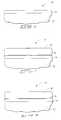
- FIG. 1is a diagrammatic perspective view of a semiconductor wafer fragment/section in process in accordance with an aspect of the invention.
- FIG. 2is a view of the FIG. 1 wafer fragment at a processing step subsequent to that shown by FIG. 1 .
- FIG. 3is a view of the FIG. 2 wafer fragment at a processing step subsequent to that shown by FIG. 2 .
- FIG. 4is a view of the FIG. 3 wafer fragment at a processing step subsequent to that shown by FIG. 3 .
- FIG. 5is a view of the FIG. 4 wafer fragment at a processing step subsequent to that shown by FIG. 4 .
- FIG. 6is a view of the FIG. 5 wafer fragment at a processing step subsequent to that shown by FIG. 5 .
- FIG. 7is a view of the FIG. 6 wafer fragment at a processing step subsequent to that shown by FIG. 6 .
- FIG. 8is a view of the FIG. 7 wafer fragment at a processing step subsequent to that shown by FIG. 7 .
- FIG. 9is a view of the FIG. 8 wafer fragment at a processing step subsequent to that shown by FIG. 8 .
- FIG. 1A semiconductor wafer fragment in process, in accordance with the preferred implementation of the invention, is depicted in FIG. 1 with the numeral 10 .
- Suchcomprises a bulk monocrystalline silicon substrate 12 having a silicon nitride comprising layer 14 formed thereover.
- semiconductor substrateor “semiconductive substrate” is defined to mean any construction comprising semiconductive material, including, but not limited to, bulk semiconductive materials such as a semiconductive wafer (either alone or in assemblies comprising other materials thereon), and semiconductive material layers (either alone or in assemblies comprising other materials).
- substraterefers to any supporting structure, including, but not limited to, the semiconductive substrates described above.
- the term “layer”encompasses both the singular and the plural unless otherwise indicated.
- an antireflective coating 16has been formed over the substrate 10 of FIG. 1 .
- Antireflective coating 16comprises both germanium and selenium.
- the antireflective coatingcontains at least 30 atomic percent germanium and at least 50 atomic percent selenium. More specifically, a more preferred concentration range for the germanium is from 30 atomic percent to 50 atomic percent, more preferably from about 38 atomic percent to about 42 atomic percent, with 40 atomic percent being a specific preferred example. A specific preferred concentration for the selenium is 60 atomic percent.
- the antireflective coatingconsists essentially of germanium and selenium.
- An example process for depositing the germanium and selenium comprising materialincludes physical vapor deposition, such as for example sputtering using a target comprised of Ge x Se y , with exemplary ranges for “x” and “y” being from 0.38 to 0.42 and from 0.58 to 0.62, respectively.
- An exemplary preferred thickness range for layer 16is from 100 Angstroms to 500 Angstroms.
- antireflective coating 16is substantially amorphous. In the context of this document, “substantially amorphous” means being at least 90 percent by volume in the amorphous phase. Further preferably, antireflective coating 16 is also homogenous.
- a layer of photoresist 18is formed over antireflective coating 16 , and preferably on (in contact therewith) antireflective coating 16 , as shown.
- Any suitable photoresistwhether existing or yet-to-be-developed, is contemplated and regardless of whether such comprises a positive or negative type photoresist.
- exemplary photoresistsinclude stepper operable photoresists, such as MIO84 and SEPR 402.
- photoresist 18has been exposed to actinic radiation (preferably, and by way of example only, using a mask or reticle) to pattern such photoresist.
- FIG. 4depicts an exemplary patterned and exposed portion 20 of layer 18 , indicated by stippling of such region entirely through layer 18 .
- Antireflective coating 16reduces reflection of the actinic radiation during the exposing than would otherwise occur under identical conditions in the absence of the antireflective coating, and thereby preferably enhances the patterned transfer to layer 18 .
- an opening 22is formed in photoresist 18 by suitable processing to remove the exemplary exposed portion depicted in FIG. 4 .
- One preferred methodis by conventional solvent processing, for example which removes the processed portion relative to the unprocessed portion, effective to form the illustrated opening 22 .
- etchingis conducted of antireflective coating 16 through photoresist openings 22 .
- Such etchingis most preferably dry and anisotropic effective to substantially transfer the opening pattern 22 within photoresist layer 18 into antireflective coating material 16 .
- Less preferredwould be wet etching of layer 16 through opening 22 .
- One exemplary dry method for removing material 16includes exposure to oxygen (i.e., O 2 ) at a temperature of less than or equal to about 100° C. in a plasma environment.
- An exemplary pressureincludes at or below 1 Torr and an applied plasma power of 1500 Watts.
- Such etchingmight also anisotropically etch some of the photoresist.
- Another exemplary processis dry etching in an ammonia containing plasma atmosphere.
- Exemplary preferred wet etchingsinclude an ammonium hydroxide solution.
- One exemplary such solutionis tetramethyl ammonium hydroxide.
- Exemplary processing conditionspreferably provide the solution at about 25° C. and atmospheric pressure with the concentration of tetramethyl ammonium hydroxide, or other ammonium hydroxide, being from about 1 percent to 50 percent by volume, with at about 2.5 percent being a specific preferred example.
- Antireflective coating 16might also be etched by these or another high pH solution, with a preferred pH being from about 9 to about 13.
- silicon nitride comprising layer 14is illustrated as having been subtractively etched through openings 22 in the photoresist and the antireflective coating using the photoresist and the antireflective coating as a mask.
- exemplary processing conditions for conducting the above-illustrated etchinclude a pressure of 20 mTorr, power at 800W, temperature from 200° C. to 600° C., CHF 3 flow at 22 sccm, and CH 2 F 2 flow at 18 sccm for from 10 seconds to 100 seconds.
- Suchprovides but one example of patterning the substrate through openings in the photoresist and the antireflective coating, using the photoresist and the antireflective coating as a mask. Any other possible alternate patterning through the openings, whether existing or yet-to-be-developed, is also of course contemplated.
- one such alternate exemplary processingwould be ion implantation into the layer or layers beneath antireflective coating material 16 as opposed to, or in addition to, subtractive etching thereof.
- photoresist layer 18has been substantially completely removed from the substrate.
- Exemplary processing for conducting the sameincludes exposure to an oxygen containing plasma, for example as referred to above.
- Wet processing to produce the illustrated FIG. 8 constructionmight also be conducted, for example, by removing the photoresist in a sulfuric acid and hydrogen peroxide solution.
- FIG. 9illustrates subsequent removal of antireflective coating 16 .
- Exemplary processes for doing soinclude any of those described above for removing material 16 to extend contact openings 22 to the underlying substrate layers.
- the inventionalso contemplates chemically etching the photoresist and the antireflective coating substantially completely from the substrate using a single etching chemistry, for example going in a substantial single etching chemistry step from the FIG. 7 to the FIG. 9 construction.
- a single etching chemistryfor example going in a substantial single etching chemistry step from the FIG. 7 to the FIG. 9 construction.
- suchmight be conducted utilizing a dry etching chemistry by exposure to an oxygen plasma containing atmosphere, preferably at a temperature above 100° C., effective to completely etch both photoresist 18 and antireflective coating 16 from the substrate, for example preferably in a single/common processing step.
- Such removal of a germanium and selenium containing antireflective coatingmight be facilitated by exposing the antireflective coating through the photoresist to radiation having a wavelength from about 190 nanometers to about 450 nanometers, and thereafter dry etching the antireflective coating in an oxygen comprising ambient. Such might be conducted as per the above for extending the photoresist openings through the antireflective coating material 16 to the underlying substrate, or in conjunction with a preferred implementation of completely removing photoresist and the antireflective coating material from the substrate using a single etching chemistry, and preferably in a single/common etching step.
- the exposing of the antireflective coating through the photoresist to radiation having a wavelength from about 190 nanometers to about 450 nanometerscould, of course, be conducted either prior to or after solvent processing of the photoresist to form the initial opening 22 therethrough.
Landscapes
- Engineering & Computer Science (AREA)
- General Physics & Mathematics (AREA)
- Physics & Mathematics (AREA)
- Microelectronics & Electronic Packaging (AREA)
- Manufacturing & Machinery (AREA)
- Computer Hardware Design (AREA)
- Condensed Matter Physics & Semiconductors (AREA)
- Power Engineering (AREA)
- Architecture (AREA)
- Structural Engineering (AREA)
- Exposure Of Semiconductors, Excluding Electron Or Ion Beam Exposure (AREA)
- Drying Of Semiconductors (AREA)
- Materials For Photolithography (AREA)
- Photosensitive Polymer And Photoresist Processing (AREA)
Abstract
Description
Claims (31)
Priority Applications (2)
| Application Number | Priority Date | Filing Date | Title |
|---|---|---|---|
| US10/071,425US7064080B2 (en) | 2002-02-08 | 2002-02-08 | Semiconductor processing method using photoresist and an antireflective coating |
| US10/719,640US6861367B2 (en) | 2002-02-08 | 2003-11-21 | Semiconductor processing method using photoresist and an antireflective coating |
Applications Claiming Priority (1)
| Application Number | Priority Date | Filing Date | Title |
|---|---|---|---|
| US10/071,425US7064080B2 (en) | 2002-02-08 | 2002-02-08 | Semiconductor processing method using photoresist and an antireflective coating |
Related Child Applications (1)
| Application Number | Title | Priority Date | Filing Date |
|---|---|---|---|
| US10/719,640DivisionUS6861367B2 (en) | 2002-02-08 | 2003-11-21 | Semiconductor processing method using photoresist and an antireflective coating |
Publications (2)
| Publication Number | Publication Date |
|---|---|
| US20030153190A1 US20030153190A1 (en) | 2003-08-14 |
| US7064080B2true US7064080B2 (en) | 2006-06-20 |
Family
ID=27659234
Family Applications (2)
| Application Number | Title | Priority Date | Filing Date |
|---|---|---|---|
| US10/071,425Expired - LifetimeUS7064080B2 (en) | 2002-02-08 | 2002-02-08 | Semiconductor processing method using photoresist and an antireflective coating |
| US10/719,640Expired - Fee RelatedUS6861367B2 (en) | 2002-02-08 | 2003-11-21 | Semiconductor processing method using photoresist and an antireflective coating |
Family Applications After (1)
| Application Number | Title | Priority Date | Filing Date |
|---|---|---|---|
| US10/719,640Expired - Fee RelatedUS6861367B2 (en) | 2002-02-08 | 2003-11-21 | Semiconductor processing method using photoresist and an antireflective coating |
Country Status (1)
| Country | Link |
|---|---|
| US (2) | US7064080B2 (en) |
Cited By (6)
| Publication number | Priority date | Publication date | Assignee | Title |
|---|---|---|---|---|
| US20070154851A1 (en)* | 2003-11-28 | 2007-07-05 | Ahn Sang H | Maintenance of photoresist adhesion on the surface of dielectric arcs for 90 NM feature sizes |
| US20080121859A1 (en)* | 2006-10-19 | 2008-05-29 | Boise State University | Forced ion migration for chalcogenide phase change memory device |
| US20100027324A1 (en)* | 2008-08-01 | 2010-02-04 | Boise State University | Variable integrated analog resistor |
| US20110079709A1 (en)* | 2009-10-07 | 2011-04-07 | Campbell Kristy A | Wide band sensor |
| US8284590B2 (en) | 2010-05-06 | 2012-10-09 | Boise State University | Integratable programmable capacitive device |
| US8467236B2 (en) | 2008-08-01 | 2013-06-18 | Boise State University | Continuously variable resistor |
Families Citing this family (12)
| Publication number | Priority date | Publication date | Assignee | Title |
|---|---|---|---|---|
| US7265431B2 (en)* | 2002-05-17 | 2007-09-04 | Intel Corporation | Imageable bottom anti-reflective coating for high resolution lithography |
| US8519540B2 (en)* | 2009-06-16 | 2013-08-27 | International Business Machines Corporation | Self-aligned dual damascene BEOL structures with patternable low- K material and methods of forming same |
| US8659115B2 (en)* | 2009-06-17 | 2014-02-25 | International Business Machines Corporation | Airgap-containing interconnect structure with improved patternable low-K material and method of fabricating |
| US8163658B2 (en)* | 2009-08-24 | 2012-04-24 | International Business Machines Corporation | Multiple patterning using improved patternable low-k dielectric materials |
| US8202783B2 (en) | 2009-09-29 | 2012-06-19 | International Business Machines Corporation | Patternable low-k dielectric interconnect structure with a graded cap layer and method of fabrication |
| US8637395B2 (en)* | 2009-11-16 | 2014-01-28 | International Business Machines Corporation | Methods for photo-patternable low-k (PPLK) integration with curing after pattern transfer |
| US8367540B2 (en)* | 2009-11-19 | 2013-02-05 | International Business Machines Corporation | Interconnect structure including a modified photoresist as a permanent interconnect dielectric and method of fabricating same |
| US8642252B2 (en) | 2010-03-10 | 2014-02-04 | International Business Machines Corporation | Methods for fabrication of an air gap-containing interconnect structure |
| US8896120B2 (en) | 2010-04-27 | 2014-11-25 | International Business Machines Corporation | Structures and methods for air gap integration |
| US8241992B2 (en) | 2010-05-10 | 2012-08-14 | International Business Machines Corporation | Method for air gap interconnect integration using photo-patternable low k material |
| US8373271B2 (en) | 2010-05-27 | 2013-02-12 | International Business Machines Corporation | Interconnect structure with an oxygen-doped SiC antireflective coating and method of fabrication |
| US20120001061A1 (en)* | 2010-07-02 | 2012-01-05 | Hamilton Sundstrand Corporation | Ion implanted beam dump |
Citations (5)
| Publication number | Priority date | Publication date | Assignee | Title |
|---|---|---|---|---|
| US4127414A (en) | 1976-06-08 | 1978-11-28 | Nippon Telegraph And Telephone Public Corporation | Pattern-forming materials having a radiation sensitive chalcogenide layer and a method of forming patterns with such materials |
| US4320191A (en)* | 1978-11-07 | 1982-03-16 | Nippon Telegraph & Telephone Public Corporation | Pattern-forming process |
| US4368099A (en) | 1982-02-05 | 1983-01-11 | Rca Corporation | Development of germanium selenide photoresist |
| JPS60226123A (en)* | 1984-04-25 | 1985-11-11 | Toshiba Corp | Pattern formation |
| US6350559B1 (en) | 1999-09-17 | 2002-02-26 | Advanced Micro Devices, Inc. | Method for creating thinner resist coating that also has fewer pinholes |
- 2002
- 2002-02-08USUS10/071,425patent/US7064080B2/ennot_activeExpired - Lifetime
- 2003
- 2003-11-21USUS10/719,640patent/US6861367B2/ennot_activeExpired - Fee Related
Patent Citations (5)
| Publication number | Priority date | Publication date | Assignee | Title |
|---|---|---|---|---|
| US4127414A (en) | 1976-06-08 | 1978-11-28 | Nippon Telegraph And Telephone Public Corporation | Pattern-forming materials having a radiation sensitive chalcogenide layer and a method of forming patterns with such materials |
| US4320191A (en)* | 1978-11-07 | 1982-03-16 | Nippon Telegraph & Telephone Public Corporation | Pattern-forming process |
| US4368099A (en) | 1982-02-05 | 1983-01-11 | Rca Corporation | Development of germanium selenide photoresist |
| JPS60226123A (en)* | 1984-04-25 | 1985-11-11 | Toshiba Corp | Pattern formation |
| US6350559B1 (en) | 1999-09-17 | 2002-02-26 | Advanced Micro Devices, Inc. | Method for creating thinner resist coating that also has fewer pinholes |
Non-Patent Citations (1)
| Title |
|---|
| Lee et al., Lithographic Properties of SiN<SUB>x</SUB>and Se<SUB>75</SUB>Ge<SUB>25</SUB>Thin Films as the Low-Energy Ion-Beam Resist, 5<SUP>th</SUP>International Conference on Properties and Applications of Dielectric Materials, Seoul, Korea (May 25-30, 1997) pp. 635-638. |
Cited By (11)
| Publication number | Priority date | Publication date | Assignee | Title |
|---|---|---|---|---|
| US20070154851A1 (en)* | 2003-11-28 | 2007-07-05 | Ahn Sang H | Maintenance of photoresist adhesion on the surface of dielectric arcs for 90 NM feature sizes |
| US8088563B2 (en)* | 2003-11-28 | 2012-01-03 | Applied Materials, Inc. | Reduction in photoresist footing undercut during development of feature sizes of 120NM or less |
| US20080121859A1 (en)* | 2006-10-19 | 2008-05-29 | Boise State University | Forced ion migration for chalcogenide phase change memory device |
| US7924608B2 (en) | 2006-10-19 | 2011-04-12 | Boise State University | Forced ion migration for chalcogenide phase change memory device |
| US8295081B2 (en) | 2006-10-19 | 2012-10-23 | Boise State University | Forced ion migration for chalcogenide phase change memory device |
| US8611146B2 (en) | 2006-10-19 | 2013-12-17 | Boise State University | Forced ion migration for chalcogenide phase change memory device |
| US20100027324A1 (en)* | 2008-08-01 | 2010-02-04 | Boise State University | Variable integrated analog resistor |
| US8238146B2 (en) | 2008-08-01 | 2012-08-07 | Boise State University | Variable integrated analog resistor |
| US8467236B2 (en) | 2008-08-01 | 2013-06-18 | Boise State University | Continuously variable resistor |
| US20110079709A1 (en)* | 2009-10-07 | 2011-04-07 | Campbell Kristy A | Wide band sensor |
| US8284590B2 (en) | 2010-05-06 | 2012-10-09 | Boise State University | Integratable programmable capacitive device |
Also Published As
| Publication number | Publication date |
|---|---|
| US20040102046A1 (en) | 2004-05-27 |
| US6861367B2 (en) | 2005-03-01 |
| US20030153190A1 (en) | 2003-08-14 |
Similar Documents
| Publication | Publication Date | Title |
|---|---|---|
| US7064080B2 (en) | Semiconductor processing method using photoresist and an antireflective coating | |
| US20220367186A1 (en) | Patterning scheme to improve euv resist and hard mask selectivity | |
| US8158335B2 (en) | High etch resistant material for double patterning | |
| US8153350B2 (en) | Method and material for forming high etch resistant double exposure patterns | |
| US7432212B2 (en) | Methods of processing a semiconductor substrate | |
| US7846843B2 (en) | Method for manufacturing a semiconductor device using a spacer as an etch mask for forming a fine pattern | |
| US20070037410A1 (en) | Method for forming a lithography pattern | |
| JP3542118B2 (en) | Formation of non-reflective material layer, semiconductor manufacturing method using the same, and method of forming transistor gate stack | |
| WO2006073871A1 (en) | Line edge roughness reduction compatible with trimming | |
| WO2004102274A2 (en) | Use of spin-on, photopatternable, interplayer dielectric materials and intermediate semiconductor device structure utilizing the same | |
| JP2013243384A (en) | Double exposure patterning by carbonaceous hard mask | |
| US8303831B2 (en) | Methods for fabricating semiconductor devices | |
| US9880473B2 (en) | Surface treatment method for dielectric anti-reflective coating (DARC) to shrink photoresist critical dimension (CD) | |
| US7611825B2 (en) | Photolithography method to prevent photoresist pattern collapse | |
| US20030194647A1 (en) | Composite photoresist for pattern transferring | |
| US20070161255A1 (en) | Method for etching with hardmask | |
| US6420095B1 (en) | Manufacture of semiconductor device using A-C anti-reflection coating | |
| JP2000315684A (en) | Method for etching | |
| JP3918488B2 (en) | Wiring formation method | |
| WO2025039435A1 (en) | High-resolution contact hole pattern structure having improved feature size, and preparation method therefor | |
| CN111696862A (en) | Semiconductor structure and forming method thereof | |
| US7195716B2 (en) | Etching process and patterning process | |
| TW200303583A (en) | Method for forming a pattern in a semiconductor substrate | |
| TW202534791A (en) | Method to pattern a semiconductor substrate using a multilayer photoresist film stack | |
| KR20020056016A (en) | Method for fabricating minute pattern |
Legal Events
| Date | Code | Title | Description |
|---|---|---|---|
| AS | Assignment | Owner name:FUJI PHOTO FILM CO., LTD., JAPAN Free format text:ASSIGNMENT OF ASSIGNORS INTEREST;ASSIGNOR:OOHASHI, HIDEKAZU;REEL/FRAME:012561/0483 Effective date:20020124 | |
| AS | Assignment | Owner name:MICRON TECHNOLOGY, INC., IDAHO Free format text:ASSIGNMENT OF ASSIGNORS INTEREST;ASSIGNORS:GILTON, TERRY L.;BOWES, STEVE W.;MOORE, JOHN T.;AND OTHERS;REEL/FRAME:012577/0332;SIGNING DATES FROM 20020129 TO 20020130 | |
| FEPP | Fee payment procedure | Free format text:PAYOR NUMBER ASSIGNED (ORIGINAL EVENT CODE: ASPN); ENTITY STATUS OF PATENT OWNER: LARGE ENTITY | |
| STCF | Information on status: patent grant | Free format text:PATENTED CASE | |
| CC | Certificate of correction | ||
| FPAY | Fee payment | Year of fee payment:4 | |
| FPAY | Fee payment | Year of fee payment:8 | |
| AS | Assignment | Owner name:U.S. BANK NATIONAL ASSOCIATION, AS COLLATERAL AGENT, CALIFORNIA Free format text:SECURITY INTEREST;ASSIGNOR:MICRON TECHNOLOGY, INC.;REEL/FRAME:038669/0001 Effective date:20160426 Owner name:U.S. BANK NATIONAL ASSOCIATION, AS COLLATERAL AGEN Free format text:SECURITY INTEREST;ASSIGNOR:MICRON TECHNOLOGY, INC.;REEL/FRAME:038669/0001 Effective date:20160426 | |
| AS | Assignment | Owner name:MORGAN STANLEY SENIOR FUNDING, INC., AS COLLATERAL AGENT, MARYLAND Free format text:PATENT SECURITY AGREEMENT;ASSIGNOR:MICRON TECHNOLOGY, INC.;REEL/FRAME:038954/0001 Effective date:20160426 Owner name:MORGAN STANLEY SENIOR FUNDING, INC., AS COLLATERAL Free format text:PATENT SECURITY AGREEMENT;ASSIGNOR:MICRON TECHNOLOGY, INC.;REEL/FRAME:038954/0001 Effective date:20160426 | |
| AS | Assignment | Owner name:U.S. BANK NATIONAL ASSOCIATION, AS COLLATERAL AGENT, CALIFORNIA Free format text:CORRECTIVE ASSIGNMENT TO CORRECT THE REPLACE ERRONEOUSLY FILED PATENT #7358718 WITH THE CORRECT PATENT #7358178 PREVIOUSLY RECORDED ON REEL 038669 FRAME 0001. ASSIGNOR(S) HEREBY CONFIRMS THE SECURITY INTEREST;ASSIGNOR:MICRON TECHNOLOGY, INC.;REEL/FRAME:043079/0001 Effective date:20160426 Owner name:U.S. BANK NATIONAL ASSOCIATION, AS COLLATERAL AGEN Free format text:CORRECTIVE ASSIGNMENT TO CORRECT THE REPLACE ERRONEOUSLY FILED PATENT #7358718 WITH THE CORRECT PATENT #7358178 PREVIOUSLY RECORDED ON REEL 038669 FRAME 0001. ASSIGNOR(S) HEREBY CONFIRMS THE SECURITY INTEREST;ASSIGNOR:MICRON TECHNOLOGY, INC.;REEL/FRAME:043079/0001 Effective date:20160426 | |
| MAFP | Maintenance fee payment | Free format text:PAYMENT OF MAINTENANCE FEE, 12TH YEAR, LARGE ENTITY (ORIGINAL EVENT CODE: M1553) Year of fee payment:12 | |
| AS | Assignment | Owner name:JPMORGAN CHASE BANK, N.A., AS COLLATERAL AGENT, ILLINOIS Free format text:SECURITY INTEREST;ASSIGNORS:MICRON TECHNOLOGY, INC.;MICRON SEMICONDUCTOR PRODUCTS, INC.;REEL/FRAME:047540/0001 Effective date:20180703 Owner name:JPMORGAN CHASE BANK, N.A., AS COLLATERAL AGENT, IL Free format text:SECURITY INTEREST;ASSIGNORS:MICRON TECHNOLOGY, INC.;MICRON SEMICONDUCTOR PRODUCTS, INC.;REEL/FRAME:047540/0001 Effective date:20180703 | |
| AS | Assignment | Owner name:MICRON TECHNOLOGY, INC., IDAHO Free format text:RELEASE BY SECURED PARTY;ASSIGNOR:U.S. BANK NATIONAL ASSOCIATION, AS COLLATERAL AGENT;REEL/FRAME:047243/0001 Effective date:20180629 | |
| AS | Assignment | Owner name:MICRON TECHNOLOGY, INC., IDAHO Free format text:RELEASE BY SECURED PARTY;ASSIGNOR:MORGAN STANLEY SENIOR FUNDING, INC., AS COLLATERAL AGENT;REEL/FRAME:050937/0001 Effective date:20190731 | |
| AS | Assignment | Owner name:MICRON TECHNOLOGY, INC., IDAHO Free format text:RELEASE BY SECURED PARTY;ASSIGNOR:JPMORGAN CHASE BANK, N.A., AS COLLATERAL AGENT;REEL/FRAME:051028/0001 Effective date:20190731 Owner name:MICRON SEMICONDUCTOR PRODUCTS, INC., IDAHO Free format text:RELEASE BY SECURED PARTY;ASSIGNOR:JPMORGAN CHASE BANK, N.A., AS COLLATERAL AGENT;REEL/FRAME:051028/0001 Effective date:20190731 |