US7061784B2 - Semiconductor memory module - Google Patents
Semiconductor memory moduleDownload PDFInfo
- Publication number
- US7061784B2 US7061784B2US10/886,814US88681404AUS7061784B2US 7061784 B2US7061784 B2US 7061784B2US 88681404 AUS88681404 AUS 88681404AUS 7061784 B2US7061784 B2US 7061784B2
- Authority
- US
- United States
- Prior art keywords
- command
- buffer chip
- clock
- address
- data
- Prior art date
- Legal status (The legal status is an assumption and is not a legal conclusion. Google has not performed a legal analysis and makes no representation as to the accuracy of the status listed.)
- Expired - Fee Related, expires
Links
- 239000004065semiconductorSubstances0.000titleclaimsabstractdescription26
- 230000003111delayed effectEffects0.000description2
- 230000006978adaptationEffects0.000description1
- 230000005540biological transmissionEffects0.000description1
- 230000002441reversible effectEffects0.000description1
- 230000002123temporal effectEffects0.000description1
Images


Classifications
- G—PHYSICS
- G11—INFORMATION STORAGE
- G11C—STATIC STORES
- G11C11/00—Digital stores characterised by the use of particular electric or magnetic storage elements; Storage elements therefor
- G11C11/21—Digital stores characterised by the use of particular electric or magnetic storage elements; Storage elements therefor using electric elements
- G11C11/34—Digital stores characterised by the use of particular electric or magnetic storage elements; Storage elements therefor using electric elements using semiconductor devices
- G11C11/40—Digital stores characterised by the use of particular electric or magnetic storage elements; Storage elements therefor using electric elements using semiconductor devices using transistors
- G11C11/401—Digital stores characterised by the use of particular electric or magnetic storage elements; Storage elements therefor using electric elements using semiconductor devices using transistors forming cells needing refreshing or charge regeneration, i.e. dynamic cells
- G11C11/4063—Auxiliary circuits, e.g. for addressing, decoding, driving, writing, sensing or timing
- G11C11/407—Auxiliary circuits, e.g. for addressing, decoding, driving, writing, sensing or timing for memory cells of the field-effect type
- G11C11/409—Read-write [R-W] circuits
- G11C11/4093—Input/output [I/O] data interface arrangements, e.g. data buffers
- G—PHYSICS
- G11—INFORMATION STORAGE
- G11C—STATIC STORES
- G11C5/00—Details of stores covered by group G11C11/00
- G11C5/06—Arrangements for interconnecting storage elements electrically, e.g. by wiring
- G11C5/063—Voltage and signal distribution in integrated semi-conductor memory access lines, e.g. word-line, bit-line, cross-over resistance, propagation delay
- G—PHYSICS
- G11—INFORMATION STORAGE
- G11C—STATIC STORES
- G11C7/00—Arrangements for writing information into, or reading information out from, a digital store
- G11C7/10—Input/output [I/O] data interface arrangements, e.g. I/O data control circuits, I/O data buffers
Definitions
- the inventionrelates to a semiconductor memory module having at least one memory chip and a buffer chip, which drives clock, address and command signals to the memory chip and drives data signals to, and receives them from, the memory chip via a module-internal clock, address, command and data bus, the buffer chip forming an interface to an external memory main bus.
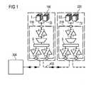
- FIG. 1illustrates a memory system of this type, in which the buffer chips 110 , 210 which are situated on respective memory modules 100 , 200 are connected in concatenated fashion to a memory main bus 400 , which leads to a memory controller 300 .
- a switching arrangement Sensures that data are read from, or written to, the respectively addressed memory module 100 or 200 only.
- the Roman numerals I, II, III and IVare used to designate individual memory groups each having a plurality of memory chips which are located one behind the other in a row on the memory modules 100 and 200 .
- the buffer chips 110 , 210convert the so-called “stub bus”, as is used nowadays in DDR and DDR-II systems, into a type of hierarchical bus system in which only point-to-point or point-to-two-point connections now occur. Connections of this type allow data transfer rates of well above one Gbps. In addition, cascading allows the concatenation of a large number of buffer chips and the realization of memory systems having a very large number of memory chips on just one memory main bus 400 .
- FIG. 2illustrates in the form of a diagrammatic layout view, the manner in which a memory module (DIMM) having a buffer chip 110 (HUB) and eight memory chips can be internally constructed.
- Clock signal lineswhich are depicted by dash-dotted lines
- C/Acommand and address bus lines
- DRAMsare driven centrally by the buffer chip 110 , successively routed to the memory chips 101 , 102 , . . . 108 (DRAMs) in a so-called fly-by topology and terminated at the end by means of terminations a 1 , a 2 , b 1 , b 2 in order to avoid signal reflections.
- the data bus lines (DQ)(illustrated by means of solid lines in FIG. 2 ) of the DRAMs are connected to the buffer chip 110 separately in the form of point-to-point connections.
- the propagation time of the signals on the abovementioned connecting lineswill play a significant part at the high frequencies at which future computer systems, and thus the memory systems thereof, will be operated. 200 ps for each path (buffer chip to DRAM and DRAM to DRAM) shall respectively be assumed below for said propagation time. All signals (CLK, C/A, DQ, DQS) therefore require 200 ps in order to pass from the buffer chip 110 to the first DRAM (for example 104 ) and 800 ps in order to pass from the buffer chip 110 to the fourth DRAM (for example 101 ). Since the clock signal CLK and the command and address signal C/A have the same propagation time, commands and addresses can be transmitted without any problems from the buffer chip 110 to the respective DRAM chip. The same applies to the transmission of write data (DQ, DQS) to the DRAMs. From the point of view of the overall system, the fact that the actual write operation in the DRAMs respectively takes place at a different time is only of secondary importance.
- the DRAM chipsreceive the read command at different times on account of the propagation times of the CLK signals and the C/A signals on the bus.
- the difference between the first and the last DRAMis 600 ps in our example.
- the DRAM chipsAfter a certain amount of time, which shall be assumed to be the same for all DRAMs, the DRAM chips begin to send their data back to the buffer chip 110 .
- the propagation time from the DRAM chip to the buffer chipnow again depends on the position of the DRAM chip on the memory module (DIMM), the propagation time in the case of this arrangement being longest for that DRAM chip which received the command last.
- DIMMmemory module
- the inventionis a memory module of the type mentioned initially such that the unavoidable time differences for command and address signals and for the write/read data are compensated for.
- a semiconductor memory moduleis distinguished by the fact that the data bus lines and/or the clock, command and address bus lines are respectively connected to the buffer chip at their two ends and can be driven by the buffer chip from these two ends. Control means are provided and set up in such a manner that they respectively match the directions of propagation of the data signals and of the clock, command and address signals on the corresponding bus lines during writing and reading.
- the buffer chipIf the buffer chip is connected to both ends of the DQ bus, during a write operation it can drive the data from the same end as that at which clock signals and command/address signals are also driven. This means that the data arrive at the memory chip in synchronism with the clock signal. During a read operation, the data are now no longer read at said end of the DQ bus but rather at the other end, with the result that clock, command, address and read data DQ move in the same direction. Since the buffer chip cannot physically be located at both ends of a linear bus, the DQ bus is, for this purpose, closed or folded to form a loop on the memory module.
- the command/address buscan be driven at both ends and the data bus can be connected on only one side.
- the command/address signalsare driven from the same end as the data signals on the data bus lines during writing and at the other end during reading.
- the datamove in the same direction as the command/address signals during writing and reading. During a read operation, this results in the data arriving at the buffer chip at virtually the same time.
- the data reception stage of the lattercan therefore be constructed in a much simpler manner and the system can be operated at considerably higher frequencies.
- FIG. 1illustrates the topology of a conventional memory system having concatenated buffer chips.
- FIG. 2illustrates the diagrammatic layout view of a conventional semiconductor memory module having a buffer chip and eight memory chips.
- FIG. 3diagrammatically illustrates a layout view of a semiconductor memory module according to the invention having a buffer chip and a loop bus via four memory chips which are arranged one behind the other in a row.
- FIGS. 4A and 4Brespectively illustrate a diagrammatic plan view and a sectional view of a DIMM semiconductor memory module for the purpose of illustrating the physical realization of the loop bus via a plurality of memory chips on the front and rear sides of the DIMM memory module and with vias on the edge of the latter.
- FIG. 5diagrammatically illustrates a semiconductor memory module in accordance with the invention for the purpose of illustrating the flow of data via the loop bus.
- FIG. 3which illustrates a diagrammatic layout view of a semiconductor memory module 100 according to the invention
- the data bus lines DQ, DQS of, for example, four memory chipsare connected according to the invention to a single buffer chip 10 at both ends.
- the fact that the command and address bus lines C/A and also the clock lines CLK of the module-internal bus 12 can also be connected to the buffer chip 10 on both sidesis indicated by means of dashed lines.
- the buffer chip 10has a control device 11 , which, in an alternative embodiment, ensures that the clock signal CLK, command and address signals C/A and data signals DQ, DQS move in the same direction when writing data. That is, during the write operation, the control device 11 situated in the buffer chip 10 ensures that the data bus lines DQ, DQS are driven at that end which coincides with the driving end of the clock bus lines CLK and of the command and address bus lines.
- the control device 11also ensures that the clock signals CLK and the command and address signals C/A and data signals DQ, DQS likewise move in the same direction, that is, the data at the buffer chip 10 are received at the other end of the DQ bus loop.
- the temporal offset between the memory chipsis precisely compensated for again during command reception by the different propagation times of the data along the loop.
- the respective non-driven end of the data bus lines DQ, DQSis terminated, in particular actively terminated, by the buffer chip 10 in order to avoid signal reflections at the end of the lines.
- clock lines CLK and command and address lines C/Amay likewise be routed back to the buffer chip 10 in the manner of a loop.
- the data bus lines DQ/DQSmay also alternatively be connected to the buffer chip 10 on only one side if both ends of the command and address lines C/A are connected to the buffer chip 10 . In this case, for read commands, the direction of propagation or travel of signals on the clock lines CLK and on the command and address lines C/A is reversed, that is, the latter are driven at that end which is opposite to the DQ end of the loop.
- FIG. 4Aillustrates a diagrammatic plan view of one side of such a DIMM semiconductor memory module 100 , which has been fitted with DRAMs and a buffer chip 10 .
- connecting linesare first of all routed from the buffer chip 10 to a plurality of DRAMs 1 – 8 on one side of the semiconductor memory module and are then plated through, by means of vias, to the other side where they are connected to further DRAM chips 9 – 16 and routed back to the buffer chip 10 .
- FIG. 5illustrates the flow of data on a semiconductor memory module according to the invention, in particular a DIMM module having a loop bus according to the invention.
- the buffer chip 10is illustrated in a U-shaped manner merely for the purposes of simplification, as a result of which it was possible to avoid a confusing illustration of loops of a large number of parallel lines.
- the Roman numeral IIis used in FIGS. 3 and 5 to indicate the connection to the other side of the module.
Landscapes
- Engineering & Computer Science (AREA)
- Microelectronics & Electronic Packaging (AREA)
- Computer Hardware Design (AREA)
- Dram (AREA)
Abstract
Description
Claims (10)
Applications Claiming Priority (2)
| Application Number | Priority Date | Filing Date | Title |
|---|---|---|---|
| DE10330811.3 | 2003-07-08 | ||
| DE10330811ADE10330811B4 (en) | 2003-07-08 | 2003-07-08 | Semiconductor memory module |
Publications (2)
| Publication Number | Publication Date |
|---|---|
| US20050024963A1 US20050024963A1 (en) | 2005-02-03 |
| US7061784B2true US7061784B2 (en) | 2006-06-13 |
Family
ID=34071595
Family Applications (1)
| Application Number | Title | Priority Date | Filing Date |
|---|---|---|---|
| US10/886,814Expired - Fee RelatedUS7061784B2 (en) | 2003-07-08 | 2004-07-08 | Semiconductor memory module |
Country Status (2)
| Country | Link |
|---|---|
| US (1) | US7061784B2 (en) |
| DE (1) | DE10330811B4 (en) |
Cited By (46)
| Publication number | Priority date | Publication date | Assignee | Title |
|---|---|---|---|---|
| US20060139983A1 (en)* | 2004-12-23 | 2006-06-29 | Sprietsma John T | Memory module routing |
| US20060274562A1 (en)* | 2005-06-06 | 2006-12-07 | International Business Machines Corporation | Planar array contact memory cards |
| US20070058408A1 (en)* | 2005-09-15 | 2007-03-15 | Hermann Ruckerbauer | Semiconductor memory array with serial control/address bus |
| US20080071956A1 (en)* | 2006-09-18 | 2008-03-20 | Qimonda Ag | Memory Apparatus with a Bus Architecture |
| US7379316B2 (en) | 2005-09-02 | 2008-05-27 | Metaram, Inc. | Methods and apparatus of stacking DRAMs |
| US7386656B2 (en) | 2006-07-31 | 2008-06-10 | Metaram, Inc. | Interface circuit system and method for performing power management operations in conjunction with only a portion of a memory circuit |
| US7392338B2 (en) | 2006-07-31 | 2008-06-24 | Metaram, Inc. | Interface circuit system and method for autonomously performing power management operations in conjunction with a plurality of memory circuits |
| US20080291747A1 (en)* | 2007-05-24 | 2008-11-27 | Staktek Group L.P. | Buffered Memory Device |
| US7472220B2 (en) | 2006-07-31 | 2008-12-30 | Metaram, Inc. | Interface circuit system and method for performing power management operations utilizing power management signals |
| US7515453B2 (en) | 2005-06-24 | 2009-04-07 | Metaram, Inc. | Integrated memory core and memory interface circuit |
| US7581127B2 (en) | 2006-07-31 | 2009-08-25 | Metaram, Inc. | Interface circuit system and method for performing power saving operations during a command-related latency |
| US7580312B2 (en) | 2006-07-31 | 2009-08-25 | Metaram, Inc. | Power saving system and method for use with a plurality of memory circuits |
| US7609567B2 (en) | 2005-06-24 | 2009-10-27 | Metaram, Inc. | System and method for simulating an aspect of a memory circuit |
| US7724589B2 (en) | 2006-07-31 | 2010-05-25 | Google Inc. | System and method for delaying a signal communicated from a system to at least one of a plurality of memory circuits |
| US8041881B2 (en) | 2006-07-31 | 2011-10-18 | Google Inc. | Memory device with emulated characteristics |
| US8055833B2 (en) | 2006-10-05 | 2011-11-08 | Google Inc. | System and method for increasing capacity, performance, and flexibility of flash storage |
| US8060774B2 (en) | 2005-06-24 | 2011-11-15 | Google Inc. | Memory systems and memory modules |
| US8077535B2 (en) | 2006-07-31 | 2011-12-13 | Google Inc. | Memory refresh apparatus and method |
| US8080874B1 (en) | 2007-09-14 | 2011-12-20 | Google Inc. | Providing additional space between an integrated circuit and a circuit board for positioning a component therebetween |
| US8081474B1 (en) | 2007-12-18 | 2011-12-20 | Google Inc. | Embossed heat spreader |
| US8090897B2 (en) | 2006-07-31 | 2012-01-03 | Google Inc. | System and method for simulating an aspect of a memory circuit |
| US8089795B2 (en) | 2006-02-09 | 2012-01-03 | Google Inc. | Memory module with memory stack and interface with enhanced capabilities |
| US8111566B1 (en) | 2007-11-16 | 2012-02-07 | Google, Inc. | Optimal channel design for memory devices for providing a high-speed memory interface |
| US8130560B1 (en) | 2006-11-13 | 2012-03-06 | Google Inc. | Multi-rank partial width memory modules |
| US8169233B2 (en) | 2009-06-09 | 2012-05-01 | Google Inc. | Programming of DIMM termination resistance values |
| US8209479B2 (en) | 2007-07-18 | 2012-06-26 | Google Inc. | Memory circuit system and method |
| US8244971B2 (en) | 2006-07-31 | 2012-08-14 | Google Inc. | Memory circuit system and method |
| US8280714B2 (en) | 2006-07-31 | 2012-10-02 | Google Inc. | Memory circuit simulation system and method with refresh capabilities |
| US8327104B2 (en) | 2006-07-31 | 2012-12-04 | Google Inc. | Adjusting the timing of signals associated with a memory system |
| US8335894B1 (en) | 2008-07-25 | 2012-12-18 | Google Inc. | Configurable memory system with interface circuit |
| US8386722B1 (en) | 2008-06-23 | 2013-02-26 | Google Inc. | Stacked DIMM memory interface |
| US8397013B1 (en) | 2006-10-05 | 2013-03-12 | Google Inc. | Hybrid memory module |
| US8438328B2 (en) | 2008-02-21 | 2013-05-07 | Google Inc. | Emulation of abstracted DIMMs using abstracted DRAMs |
| US20130208524A1 (en)* | 2012-02-14 | 2013-08-15 | Samsung Electronics Co., Ltd. | Memory module for high-speed operations |
| US8566516B2 (en) | 2006-07-31 | 2013-10-22 | Google Inc. | Refresh management of memory modules |
| US8796830B1 (en) | 2006-09-01 | 2014-08-05 | Google Inc. | Stackable low-profile lead frame package |
| US20150033050A1 (en)* | 2013-07-25 | 2015-01-29 | Samsung Electronics Co., Ltd | Semiconductor integrated circuit and computing device including the same |
| US8972673B2 (en) | 2006-07-31 | 2015-03-03 | Google Inc. | Power management of memory circuits by virtual memory simulation |
| US9171585B2 (en) | 2005-06-24 | 2015-10-27 | Google Inc. | Configurable memory circuit system and method |
| US9507739B2 (en) | 2005-06-24 | 2016-11-29 | Google Inc. | Configurable memory circuit system and method |
| US9542352B2 (en) | 2006-02-09 | 2017-01-10 | Google Inc. | System and method for reducing command scheduling constraints of memory circuits |
| US9632929B2 (en) | 2006-02-09 | 2017-04-25 | Google Inc. | Translating an address associated with a command communicated between a system and memory circuits |
| KR20180049386A (en) | 2016-11-01 | 2018-05-11 | 에스케이하이닉스 주식회사 | Memory device and memory system supporting rank-level parallelism |
| US10013371B2 (en) | 2005-06-24 | 2018-07-03 | Google Llc | Configurable memory circuit system and method |
| US10360953B2 (en)* | 2002-08-03 | 2019-07-23 | Longitude Licensing Limited | Memory system and data transmission method |
| US11742277B2 (en) | 2018-08-14 | 2023-08-29 | Rambus Inc. | Packaged integrated device having memory buffer integrated circuit asymmetrically positioned on substrate |
Families Citing this family (10)
| Publication number | Priority date | Publication date | Assignee | Title |
|---|---|---|---|---|
| DE102005043547B4 (en)* | 2005-09-13 | 2008-03-13 | Qimonda Ag | Memory module, memory device and method for operating a memory device |
| US20080025136A1 (en)* | 2006-07-31 | 2008-01-31 | Metaram, Inc. | System and method for storing at least a portion of information received in association with a first operation for use in performing a second operation |
| US20080028135A1 (en)* | 2006-07-31 | 2008-01-31 | Metaram, Inc. | Multiple-component memory interface system and method |
| US8040710B2 (en)* | 2007-05-31 | 2011-10-18 | Qimonda Ag | Semiconductor memory arrangement |
| US20090001541A1 (en)* | 2007-06-29 | 2009-01-01 | Lucent Technologies Inc. | Method and apparatus for stackable modular integrated circuits |
| DE102008010544A1 (en)* | 2008-02-22 | 2009-09-17 | Qimonda Ag | Memory module for use in e.g. personal computer, to store digital data in dynamic RAM, has termination device switchably implemented at end of command and address bus connected, where bus is guided sequentially through memory chips |
| KR101854251B1 (en)* | 2010-11-30 | 2018-05-03 | 삼성전자주식회사 | multi channel semiconductor memory device and semiconductor device having such memory device |
| US9176154B2 (en) | 2012-12-12 | 2015-11-03 | Bio-Rad Laboratories, Inc. | Calibration process and system |
| US8723329B1 (en)* | 2013-03-15 | 2014-05-13 | Invensas Corporation | In-package fly-by signaling |
| US10090236B2 (en)* | 2016-01-13 | 2018-10-02 | Advanced Micro Devices, Inc. | Interposer having a pattern of sites for mounting chiplets |
Citations (8)
| Publication number | Priority date | Publication date | Assignee | Title |
|---|---|---|---|---|
| US5867448A (en)* | 1997-06-11 | 1999-02-02 | Cypress Semiconductor Corp. | Buffer for memory modules with trace delay compensation |
| US6125419A (en)* | 1996-06-13 | 2000-09-26 | Hitachi, Ltd. | Bus system, printed circuit board, signal transmission line, series circuit and memory module |
| US6142830A (en) | 1998-03-06 | 2000-11-07 | Siemens Aktiengesellschaft | Signaling improvement using extended transmission lines on high speed DIMMS |
| EP1069509A2 (en) | 1999-07-16 | 2001-01-17 | Texas Instruments Incorporated | Improvements in or relating to microprocessors |
| US6356502B1 (en)* | 1998-10-28 | 2002-03-12 | Hyundai Electronics Industries Co., Ltd. | Address strobe signal generator for memory device |
| US6449213B1 (en)* | 2000-09-18 | 2002-09-10 | Intel Corporation | Memory interface having source-synchronous command/address signaling |
| US6530006B1 (en)* | 2000-09-18 | 2003-03-04 | Intel Corporation | System and method for providing reliable transmission in a buffered memory system |
| US20040105292A1 (en)* | 2002-08-23 | 2004-06-03 | Elpida Memory, Inc. | Memory system and data transmission method |
- 2003
- 2003-07-08DEDE10330811Apatent/DE10330811B4/ennot_activeExpired - Fee Related
- 2004
- 2004-07-08USUS10/886,814patent/US7061784B2/ennot_activeExpired - Fee Related
Patent Citations (8)
| Publication number | Priority date | Publication date | Assignee | Title |
|---|---|---|---|---|
| US6125419A (en)* | 1996-06-13 | 2000-09-26 | Hitachi, Ltd. | Bus system, printed circuit board, signal transmission line, series circuit and memory module |
| US5867448A (en)* | 1997-06-11 | 1999-02-02 | Cypress Semiconductor Corp. | Buffer for memory modules with trace delay compensation |
| US6142830A (en) | 1998-03-06 | 2000-11-07 | Siemens Aktiengesellschaft | Signaling improvement using extended transmission lines on high speed DIMMS |
| US6356502B1 (en)* | 1998-10-28 | 2002-03-12 | Hyundai Electronics Industries Co., Ltd. | Address strobe signal generator for memory device |
| EP1069509A2 (en) | 1999-07-16 | 2001-01-17 | Texas Instruments Incorporated | Improvements in or relating to microprocessors |
| US6449213B1 (en)* | 2000-09-18 | 2002-09-10 | Intel Corporation | Memory interface having source-synchronous command/address signaling |
| US6530006B1 (en)* | 2000-09-18 | 2003-03-04 | Intel Corporation | System and method for providing reliable transmission in a buffered memory system |
| US20040105292A1 (en)* | 2002-08-23 | 2004-06-03 | Elpida Memory, Inc. | Memory system and data transmission method |
Cited By (96)
| Publication number | Priority date | Publication date | Assignee | Title |
|---|---|---|---|---|
| US10360953B2 (en)* | 2002-08-03 | 2019-07-23 | Longitude Licensing Limited | Memory system and data transmission method |
| US20230018344A1 (en)* | 2002-08-23 | 2023-01-19 | Longitude Licensing Limited | Memory system and data transmission method |
| US11410712B2 (en) | 2002-08-23 | 2022-08-09 | Longitude Licensing Limited | Memory system and data transmission method |
| US20060139983A1 (en)* | 2004-12-23 | 2006-06-29 | Sprietsma John T | Memory module routing |
| US20080266778A1 (en)* | 2004-12-23 | 2008-10-30 | Intel Corporation | Memory module routing |
| US7863091B2 (en) | 2005-06-06 | 2011-01-04 | International Business Machines Corporation | Planar array contact memory cards |
| US8138592B2 (en) | 2005-06-06 | 2012-03-20 | International Business Machines Corporation | Planar array contact memory cards |
| US20080001275A1 (en)* | 2005-06-06 | 2008-01-03 | Paul Coteus | Planar Array Contact Memory Cards |
| US20060274562A1 (en)* | 2005-06-06 | 2006-12-07 | International Business Machines Corporation | Planar array contact memory cards |
| US7282790B2 (en)* | 2005-06-06 | 2007-10-16 | International Business Machines Corporation | Planar array contact memory cards |
| US20080045052A1 (en)* | 2005-06-06 | 2008-02-21 | Paul Coteus | Planar Array Contact Memory Cards |
| US7863089B2 (en) | 2005-06-06 | 2011-01-04 | International Business Machines Corporation | Planar array contact memory cards |
| US7566959B2 (en) | 2005-06-06 | 2009-07-28 | International Business Machines Corporation | Planar array contact memory cards |
| US20090075502A1 (en)* | 2005-06-06 | 2009-03-19 | International Business Machines Corporation | Planar Array Contact Memory Cards |
| US20090072372A1 (en)* | 2005-06-06 | 2009-03-19 | International Business Machines Corporation | Planar Array Contact Memory Cards |
| US9507739B2 (en) | 2005-06-24 | 2016-11-29 | Google Inc. | Configurable memory circuit system and method |
| US8359187B2 (en) | 2005-06-24 | 2013-01-22 | Google Inc. | Simulating a different number of memory circuit devices |
| US8386833B2 (en) | 2005-06-24 | 2013-02-26 | Google Inc. | Memory systems and memory modules |
| US7515453B2 (en) | 2005-06-24 | 2009-04-07 | Metaram, Inc. | Integrated memory core and memory interface circuit |
| US9171585B2 (en) | 2005-06-24 | 2015-10-27 | Google Inc. | Configurable memory circuit system and method |
| US7609567B2 (en) | 2005-06-24 | 2009-10-27 | Metaram, Inc. | System and method for simulating an aspect of a memory circuit |
| US8060774B2 (en) | 2005-06-24 | 2011-11-15 | Google Inc. | Memory systems and memory modules |
| US8615679B2 (en) | 2005-06-24 | 2013-12-24 | Google Inc. | Memory modules with reliability and serviceability functions |
| US10013371B2 (en) | 2005-06-24 | 2018-07-03 | Google Llc | Configurable memory circuit system and method |
| US7379316B2 (en) | 2005-09-02 | 2008-05-27 | Metaram, Inc. | Methods and apparatus of stacking DRAMs |
| US8582339B2 (en) | 2005-09-02 | 2013-11-12 | Google Inc. | System including memory stacks |
| US8619452B2 (en) | 2005-09-02 | 2013-12-31 | Google Inc. | Methods and apparatus of stacking DRAMs |
| US8811065B2 (en) | 2005-09-02 | 2014-08-19 | Google Inc. | Performing error detection on DRAMs |
| US20070058408A1 (en)* | 2005-09-15 | 2007-03-15 | Hermann Ruckerbauer | Semiconductor memory array with serial control/address bus |
| US7397684B2 (en)* | 2005-09-15 | 2008-07-08 | Infineon Technologies, Ag | Semiconductor memory array with serial control/address bus |
| US8797779B2 (en) | 2006-02-09 | 2014-08-05 | Google Inc. | Memory module with memory stack and interface with enhanced capabilites |
| US9632929B2 (en) | 2006-02-09 | 2017-04-25 | Google Inc. | Translating an address associated with a command communicated between a system and memory circuits |
| US8566556B2 (en) | 2006-02-09 | 2013-10-22 | Google Inc. | Memory module with memory stack and interface with enhanced capabilities |
| US9542352B2 (en) | 2006-02-09 | 2017-01-10 | Google Inc. | System and method for reducing command scheduling constraints of memory circuits |
| US9542353B2 (en) | 2006-02-09 | 2017-01-10 | Google Inc. | System and method for reducing command scheduling constraints of memory circuits |
| US8089795B2 (en) | 2006-02-09 | 2012-01-03 | Google Inc. | Memory module with memory stack and interface with enhanced capabilities |
| US9727458B2 (en) | 2006-02-09 | 2017-08-08 | Google Inc. | Translating an address associated with a command communicated between a system and memory circuits |
| US8340953B2 (en) | 2006-07-31 | 2012-12-25 | Google, Inc. | Memory circuit simulation with power saving capabilities |
| US8566516B2 (en) | 2006-07-31 | 2013-10-22 | Google Inc. | Refresh management of memory modules |
| US8154935B2 (en) | 2006-07-31 | 2012-04-10 | Google Inc. | Delaying a signal communicated from a system to at least one of a plurality of memory circuits |
| US7724589B2 (en) | 2006-07-31 | 2010-05-25 | Google Inc. | System and method for delaying a signal communicated from a system to at least one of a plurality of memory circuits |
| US8631220B2 (en) | 2006-07-31 | 2014-01-14 | Google Inc. | Adjusting the timing of signals associated with a memory system |
| US8041881B2 (en) | 2006-07-31 | 2011-10-18 | Google Inc. | Memory device with emulated characteristics |
| US8244971B2 (en) | 2006-07-31 | 2012-08-14 | Google Inc. | Memory circuit system and method |
| US8280714B2 (en) | 2006-07-31 | 2012-10-02 | Google Inc. | Memory circuit simulation system and method with refresh capabilities |
| US8327104B2 (en) | 2006-07-31 | 2012-12-04 | Google Inc. | Adjusting the timing of signals associated with a memory system |
| US7386656B2 (en) | 2006-07-31 | 2008-06-10 | Metaram, Inc. | Interface circuit system and method for performing power management operations in conjunction with only a portion of a memory circuit |
| US7392338B2 (en) | 2006-07-31 | 2008-06-24 | Metaram, Inc. | Interface circuit system and method for autonomously performing power management operations in conjunction with a plurality of memory circuits |
| US8090897B2 (en) | 2006-07-31 | 2012-01-03 | Google Inc. | System and method for simulating an aspect of a memory circuit |
| US7472220B2 (en) | 2006-07-31 | 2008-12-30 | Metaram, Inc. | Interface circuit system and method for performing power management operations utilizing power management signals |
| US8077535B2 (en) | 2006-07-31 | 2011-12-13 | Google Inc. | Memory refresh apparatus and method |
| US7581127B2 (en) | 2006-07-31 | 2009-08-25 | Metaram, Inc. | Interface circuit system and method for performing power saving operations during a command-related latency |
| US7580312B2 (en) | 2006-07-31 | 2009-08-25 | Metaram, Inc. | Power saving system and method for use with a plurality of memory circuits |
| US9047976B2 (en) | 2006-07-31 | 2015-06-02 | Google Inc. | Combined signal delay and power saving for use with a plurality of memory circuits |
| US8972673B2 (en) | 2006-07-31 | 2015-03-03 | Google Inc. | Power management of memory circuits by virtual memory simulation |
| US8868829B2 (en) | 2006-07-31 | 2014-10-21 | Google Inc. | Memory circuit system and method |
| US8745321B2 (en) | 2006-07-31 | 2014-06-03 | Google Inc. | Simulating a memory standard |
| US7590796B2 (en) | 2006-07-31 | 2009-09-15 | Metaram, Inc. | System and method for power management in memory systems |
| US8796830B1 (en) | 2006-09-01 | 2014-08-05 | Google Inc. | Stackable low-profile lead frame package |
| US7515451B2 (en) | 2006-09-18 | 2009-04-07 | Qimonda Ag | Memory apparatus with a bus architecture |
| DE102006043634B4 (en)* | 2006-09-18 | 2012-07-19 | Qimonda Ag | Semiconductor memory module with bus architecture |
| DE102006043634A1 (en)* | 2006-09-18 | 2008-03-27 | Qimonda Ag | Semiconductor memory module with bus architecture |
| US20080071956A1 (en)* | 2006-09-18 | 2008-03-20 | Qimonda Ag | Memory Apparatus with a Bus Architecture |
| US8751732B2 (en) | 2006-10-05 | 2014-06-10 | Google Inc. | System and method for increasing capacity, performance, and flexibility of flash storage |
| US8370566B2 (en) | 2006-10-05 | 2013-02-05 | Google Inc. | System and method for increasing capacity, performance, and flexibility of flash storage |
| US8055833B2 (en) | 2006-10-05 | 2011-11-08 | Google Inc. | System and method for increasing capacity, performance, and flexibility of flash storage |
| US8397013B1 (en) | 2006-10-05 | 2013-03-12 | Google Inc. | Hybrid memory module |
| US8977806B1 (en) | 2006-10-05 | 2015-03-10 | Google Inc. | Hybrid memory module |
| US8446781B1 (en) | 2006-11-13 | 2013-05-21 | Google Inc. | Multi-rank partial width memory modules |
| US8130560B1 (en) | 2006-11-13 | 2012-03-06 | Google Inc. | Multi-rank partial width memory modules |
| US8760936B1 (en) | 2006-11-13 | 2014-06-24 | Google Inc. | Multi-rank partial width memory modules |
| US20080291747A1 (en)* | 2007-05-24 | 2008-11-27 | Staktek Group L.P. | Buffered Memory Device |
| US7508723B2 (en) | 2007-05-24 | 2009-03-24 | Entorian Technologies, Lp | Buffered memory device |
| US8209479B2 (en) | 2007-07-18 | 2012-06-26 | Google Inc. | Memory circuit system and method |
| US8080874B1 (en) | 2007-09-14 | 2011-12-20 | Google Inc. | Providing additional space between an integrated circuit and a circuit board for positioning a component therebetween |
| US8675429B1 (en) | 2007-11-16 | 2014-03-18 | Google Inc. | Optimal channel design for memory devices for providing a high-speed memory interface |
| US8111566B1 (en) | 2007-11-16 | 2012-02-07 | Google, Inc. | Optimal channel design for memory devices for providing a high-speed memory interface |
| US8705240B1 (en) | 2007-12-18 | 2014-04-22 | Google Inc. | Embossed heat spreader |
| US8730670B1 (en) | 2007-12-18 | 2014-05-20 | Google Inc. | Embossed heat spreader |
| US8081474B1 (en) | 2007-12-18 | 2011-12-20 | Google Inc. | Embossed heat spreader |
| US8631193B2 (en) | 2008-02-21 | 2014-01-14 | Google Inc. | Emulation of abstracted DIMMS using abstracted DRAMS |
| US8438328B2 (en) | 2008-02-21 | 2013-05-07 | Google Inc. | Emulation of abstracted DIMMs using abstracted DRAMs |
| US8386722B1 (en) | 2008-06-23 | 2013-02-26 | Google Inc. | Stacked DIMM memory interface |
| US8762675B2 (en) | 2008-06-23 | 2014-06-24 | Google Inc. | Memory system for synchronous data transmission |
| US8819356B2 (en) | 2008-07-25 | 2014-08-26 | Google Inc. | Configurable multirank memory system with interface circuit |
| US8335894B1 (en) | 2008-07-25 | 2012-12-18 | Google Inc. | Configurable memory system with interface circuit |
| US8169233B2 (en) | 2009-06-09 | 2012-05-01 | Google Inc. | Programming of DIMM termination resistance values |
| US9082464B2 (en)* | 2012-02-14 | 2015-07-14 | Samsung Electronics Co., Ltd. | Memory module for high-speed operations |
| US20130208524A1 (en)* | 2012-02-14 | 2013-08-15 | Samsung Electronics Co., Ltd. | Memory module for high-speed operations |
| US20150033050A1 (en)* | 2013-07-25 | 2015-01-29 | Samsung Electronics Co., Ltd | Semiconductor integrated circuit and computing device including the same |
| KR20180049386A (en) | 2016-11-01 | 2018-05-11 | 에스케이하이닉스 주식회사 | Memory device and memory system supporting rank-level parallelism |
| US11113211B2 (en) | 2016-11-01 | 2021-09-07 | SK Hynix Inc. | Memory device supporting rank-level parallelism and memory system including the same |
| US11113210B2 (en) | 2016-11-01 | 2021-09-07 | SK Hynix Inc. | Memory device supporting rank-level parallelism and memory system including the same |
| US10459853B2 (en)* | 2016-11-01 | 2019-10-29 | SK Hynix Inc. | Memory device supporting rank-level parallelism and memory system including the same |
| US11742277B2 (en) | 2018-08-14 | 2023-08-29 | Rambus Inc. | Packaged integrated device having memory buffer integrated circuit asymmetrically positioned on substrate |
| US12087681B2 (en) | 2018-08-14 | 2024-09-10 | Rambus Inc. | Packaged integrated device with memory buffer integrated circuit die and memory devices on module substrate |
Also Published As
| Publication number | Publication date |
|---|---|
| DE10330811B4 (en) | 2009-08-13 |
| US20050024963A1 (en) | 2005-02-03 |
| DE10330811A1 (en) | 2005-02-17 |
Similar Documents
| Publication | Publication Date | Title |
|---|---|---|
| US7061784B2 (en) | Semiconductor memory module | |
| US7386696B2 (en) | Semiconductor memory module | |
| US6972981B2 (en) | Semiconductor memory module | |
| US20230120661A1 (en) | Semiconductor memory systems with on-die data buffering | |
| US7830692B2 (en) | Multi-chip memory device with stacked memory chips, method of stacking memory chips, and method of controlling operation of multi-chip package memory | |
| US7024518B2 (en) | Dual-port buffer-to-memory interface | |
| US6742098B1 (en) | Dual-port buffer-to-memory interface | |
| KR100541130B1 (en) | Memory module and memory system | |
| US7079446B2 (en) | DRAM interface circuits having enhanced skew, slew rate and impedance control | |
| US7804720B2 (en) | Integrated circuit memory devices including mode registers set using a data input/output bus | |
| US7274583B2 (en) | Memory system having multi-terminated multi-drop bus | |
| US8664972B2 (en) | Memory control circuit, memory control method, and integrated circuit | |
| US7861029B2 (en) | Memory module having buffer and memory ranks addressable by respective selection signal | |
| EP3234784B1 (en) | Dynamic random access memory (dram) component for high-performance,high-capacity registered memory modules | |
| US20220382691A1 (en) | Multi-Mode Memory Module and Memory Component | |
| US20100312956A1 (en) | Load reduced memory module | |
| US20050086424A1 (en) | Well-matched echo clock in memory system | |
| US6487086B2 (en) | Circuit module | |
| US20100312925A1 (en) | Load reduced memory module | |
| US20090019184A1 (en) | Interfacing memory devices | |
| US10431274B2 (en) | Semiconductor memory device | |
| US6996027B2 (en) | Synchronous memory device | |
| JP4173970B2 (en) | Memory system and memory module | |
| CN113889161A (en) | Configuring multiple register clock drivers of a memory subsystem | |
| US7515451B2 (en) | Memory apparatus with a bus architecture |
Legal Events
| Date | Code | Title | Description |
|---|---|---|---|
| AS | Assignment | Owner name:INFINEON TECHNOLOGIES AG, GERMAN DEMOCRATIC REPUBL Free format text:ASSIGNMENT OF ASSIGNORS INTEREST;ASSIGNORS:JAKOBS, ANDREAS;RUCKERBAUER, HERMANN;KUZMENKA, MAKSIM;REEL/FRAME:015902/0246;SIGNING DATES FROM 20040823 TO 20040831 | |
| FPAY | Fee payment | Year of fee payment:4 | |
| AS | Assignment | Owner name:QIMONDA AG, GERMANY Free format text:ASSIGNMENT OF ASSIGNORS INTEREST;ASSIGNOR:INFINEON TECHNOLOGIES AG;REEL/FRAME:023821/0535 Effective date:20060425 Owner name:QIMONDA AG,GERMANY Free format text:ASSIGNMENT OF ASSIGNORS INTEREST;ASSIGNOR:INFINEON TECHNOLOGIES AG;REEL/FRAME:023821/0535 Effective date:20060425 | |
| FPAY | Fee payment | Year of fee payment:8 | |
| AS | Assignment | Owner name:INFINEON TECHNOLOGIES AG, GERMANY Free format text:ASSIGNMENT OF ASSIGNORS INTEREST;ASSIGNOR:QIMONDA AG;REEL/FRAME:035623/0001 Effective date:20141009 | |
| AS | Assignment | Owner name:POLARIS INNOVATIONS LIMITED, IRELAND Free format text:ASSIGNMENT OF ASSIGNORS INTEREST;ASSIGNOR:INFINEON TECHNOLOGIES AG;REEL/FRAME:036877/0513 Effective date:20150708 | |
| FEPP | Fee payment procedure | Free format text:MAINTENANCE FEE REMINDER MAILED (ORIGINAL EVENT CODE: REM.) | |
| LAPS | Lapse for failure to pay maintenance fees | Free format text:PATENT EXPIRED FOR FAILURE TO PAY MAINTENANCE FEES (ORIGINAL EVENT CODE: EXP.) | |
| STCH | Information on status: patent discontinuation | Free format text:PATENT EXPIRED DUE TO NONPAYMENT OF MAINTENANCE FEES UNDER 37 CFR 1.362 | |
| FP | Lapsed due to failure to pay maintenance fee | Effective date:20180613 |