US7061627B2 - Optical scatterometry of asymmetric lines and structures - Google Patents
Optical scatterometry of asymmetric lines and structuresDownload PDFInfo
- Publication number
- US7061627B2 US7061627B2US10/385,863US38586303AUS7061627B2US 7061627 B2US7061627 B2US 7061627B2US 38586303 AUS38586303 AUS 38586303AUS 7061627 B2US7061627 B2US 7061627B2
- Authority
- US
- United States
- Prior art keywords
- detector
- sample
- reflected
- output signals
- probe beam
- Prior art date
- Legal status (The legal status is an assumption and is not a legal conclusion. Google has not performed a legal analysis and makes no representation as to the accuracy of the status listed.)
- Expired - Lifetime, expires
Links
- 230000003287optical effectEffects0.000titleclaimsdescription30
- 238000000034methodMethods0.000claimsabstractdescription36
- 239000000523sampleSubstances0.000claimsdescription59
- 238000005259measurementMethods0.000claimsdescription29
- 238000003491arrayMethods0.000claimsdescription15
- 230000004044responseEffects0.000claimsdescription3
- 230000000737periodic effectEffects0.000abstractdescription7
- 238000013459approachMethods0.000description10
- 238000004458analytical methodMethods0.000description9
- 238000010586diagramMethods0.000description7
- 239000004065semiconductorSubstances0.000description7
- 235000012431wafersNutrition0.000description7
- 238000004422calculation algorithmMethods0.000description4
- 238000004364calculation methodMethods0.000description4
- 238000000572ellipsometryMethods0.000description4
- 238000005516engineering processMethods0.000description4
- 230000008569processEffects0.000description4
- 230000003595spectral effectEffects0.000description4
- 230000010287polarizationEffects0.000description3
- 230000035945sensitivityEffects0.000description3
- 238000012935AveragingMethods0.000description2
- 230000001154acute effectEffects0.000description2
- 238000006073displacement reactionMethods0.000description2
- 238000005286illuminationMethods0.000description2
- 230000003993interactionEffects0.000description2
- 239000000463materialSubstances0.000description2
- 238000002310reflectometryMethods0.000description2
- 238000004611spectroscopical analysisMethods0.000description2
- 238000012897Levenberg–Marquardt algorithmMethods0.000description1
- 230000001419dependent effectEffects0.000description1
- 230000000694effectsEffects0.000description1
- 238000005530etchingMethods0.000description1
- 238000011156evaluationMethods0.000description1
- 230000006870functionEffects0.000description1
- 230000002068genetic effectEffects0.000description1
- 238000012804iterative processMethods0.000description1
- 238000012986modificationMethods0.000description1
- 230000004048modificationEffects0.000description1
- 229920002120photoresistant polymerPolymers0.000description1
- 238000012545processingMethods0.000description1
- 238000006467substitution reactionMethods0.000description1
- 230000007704transitionEffects0.000description1
Images


Classifications
- G—PHYSICS
- G03—PHOTOGRAPHY; CINEMATOGRAPHY; ANALOGOUS TECHNIQUES USING WAVES OTHER THAN OPTICAL WAVES; ELECTROGRAPHY; HOLOGRAPHY
- G03F—PHOTOMECHANICAL PRODUCTION OF TEXTURED OR PATTERNED SURFACES, e.g. FOR PRINTING, FOR PROCESSING OF SEMICONDUCTOR DEVICES; MATERIALS THEREFOR; ORIGINALS THEREFOR; APPARATUS SPECIALLY ADAPTED THEREFOR
- G03F7/00—Photomechanical, e.g. photolithographic, production of textured or patterned surfaces, e.g. printing surfaces; Materials therefor, e.g. comprising photoresists; Apparatus specially adapted therefor
- G03F7/70—Microphotolithographic exposure; Apparatus therefor
- G03F7/70483—Information management; Active and passive control; Testing; Wafer monitoring, e.g. pattern monitoring
- G03F7/70605—Workpiece metrology
- G03F7/70616—Monitoring the printed patterns
- G03F7/70625—Dimensions, e.g. line width, critical dimension [CD], profile, sidewall angle or edge roughness
- G—PHYSICS
- G03—PHOTOGRAPHY; CINEMATOGRAPHY; ANALOGOUS TECHNIQUES USING WAVES OTHER THAN OPTICAL WAVES; ELECTROGRAPHY; HOLOGRAPHY
- G03F—PHOTOMECHANICAL PRODUCTION OF TEXTURED OR PATTERNED SURFACES, e.g. FOR PRINTING, FOR PROCESSING OF SEMICONDUCTOR DEVICES; MATERIALS THEREFOR; ORIGINALS THEREFOR; APPARATUS SPECIALLY ADAPTED THEREFOR
- G03F7/00—Photomechanical, e.g. photolithographic, production of textured or patterned surfaces, e.g. printing surfaces; Materials therefor, e.g. comprising photoresists; Apparatus specially adapted therefor
- G03F7/70—Microphotolithographic exposure; Apparatus therefor
- G03F7/70483—Information management; Active and passive control; Testing; Wafer monitoring, e.g. pattern monitoring
- G03F7/70605—Workpiece metrology
- G03F7/70616—Monitoring the printed patterns
- G03F7/70633—Overlay, i.e. relative alignment between patterns printed by separate exposures in different layers, or in the same layer in multiple exposures or stitching
Definitions
- the subject inventionrelates to optical devices used to non-destructively evaluate semiconductor wafers.
- the present inventionrelates to methods for measuring asymmetric lines and structures.
- optical scatterometryi.e., diffraction
- CDcritical dimension
- overlayoptical scatterometry
- overlay registrationoverlay registration
- Optical scatterometryappears to show considerable promise for performing such measurements using some or all of the techniques described above for CD measurements, with appropriate modifications in the model and analysis.
- Asymmetric CD linesmay be the result of stepper artifacts, or from photoresist stripping or material etching processes.
- FIG. 1illustrates a simple asymmetric line pattern where the right side wall angle a is smaller than the left side wall angle ⁇
- Asymmetric overlay lines or patternsare a natural consequence of layer-to-layer misalignment.
- the problem of asymmetric linesis that in most cases it is not possible to distinguish between right and left asymmetries with conventional optical scatterometry techniques without resort to special or multiple patterns. Discussions related to the use of grating like patterns to evaluate mask overlay can be found in U.S. Pat. Nos. 4,757,207; 6,023,338 and 6,079,256, and U.S. 2002/0158193 all incorporated herein by reference.
- the present inventionprovides several methods for analyzing asymmetric structures (including isolated and periodic structures) without resort to special or multiple patterns.
- a split detectoris used to monitor the reflected probe beam in a broadband spectrometer.
- the incident probe beamis typically directed normally against the subject.
- the split detectorhas separate right and left halves. By independently measuring and comparing the right and left scattered rays, information about asymmetries can be determined.
- a second methodis to use two separate detectors in a broadband spectrometer.
- the first detectoris positioned to capture specular reflection and the second is positioned to capture non-specular reflection.
- the first detectormay be implemented using the split detector described previously. This allows information about right and left scattered rays as well as specular and non-specular reflections to be analyzed simultaneously.
- a third methodis to introduce polarized light into the probe beam in a broadband spectrometer.
- the structure being analyzede.g., line or grating
- the polarized light in the probe beamhas an angle of polarization that is greater than normal and less than parallel to the alignment of the structure.
- a fourth methodis to use a non-normal subject alignment within a spectral ellipsometer.
- the non-normal alignmentcauses the incident plane of the probe beam to intersect the structure being analyzed (typically a line or grating) at a non-normal angle. For typical implementations, this angle is forty-five degrees.
- Another method for analyzing asymmetric structuresis to selectively process the detector output of the detectors within a beam profile reflectometry (BPR) system or beam profile ellipsometry (BPE) system.
- BPRbeam profile reflectometry
- BPEbeam profile ellipsometry
- the detectors in BPR/BPE systemsare typically configured to include two linear detector arrays.
- the detectors arraysare typically oriented perpendicularly to each other to provide coverage in two dimensions.
- This type of detectorcan be used to evaluate asymmetries in two axes. For example, if the line or grating structure is parallel to one detector array, it is perpendicular to the second detector array. The perpendicular relationship positions the two halves of the second detector array on opposite sides of the asymmetric structure. By comparing the separate output of the two halves of the second detector array, information about asymmetries can be determined.
- the parallel/perpendicular alignmentmay be replaced by an orientation where the line or grating structure is aligned at an acute angle to both detector arrays.
- An examplewould be an implementation where the line or grating structure is aligned at a forty-five degree angle to both detector arrays.
- the analysis hereis similar to the case of parallel/perpendicular alignment except that the output of both halves of both detector arrays is considered. It other cases, it is possible to use a full two dimensional array of detectors (e.g., a grid). A detector array of this type allows asymmetries to be determined along any axis.
- Scanning BPR/BPE systemsmay also be implemented to examine asymmetric structures.
- the subjectis moved translationally during the measurements process.
- Detector outputis recorded as a function of translational position.
- the position/output informationis used to determine information about asymmetries.
- the methods described aboverelate to both CD measurements of asymmetric lines and overlay measurements to distinguish whether overlay displacement is to the right or left of a line.
- the methods described abovealso include any and all possible combinations of SE, BB, BPR and BPE with CD and overlay capability. More specifically, it is known that measurement information from various technologies can be combined to improve the analysis of an unknown sample. Examples of combining measurement technologies are disclosed in some of the above cited references as well as in U.S. Pat. No. 6,278,519 incorporated herein by reference. A combination of information can be relatively simple such as averaging the results from two different measurements. Preferably, all of the measurements are combined and applied to a theoretical model to permit simultaneous regression to an optimal solution.
- FIG. 1is a perspective view of a semiconductor wafer including an asymmetric grating shown as a typical subject for the present invention.
- FIG. 2is a block diagram of a broadband spectrometer using a split detector as provided by the present invention.
- FIG. 3is a block diagram of a split detector as provided by the present invention.
- FIG. 4is a block diagram of a broadband spectrometer using two detectors as provided by the present invention.
- FIG. 5is a perspective view showing the interaction of a probe beam including a polarized component generated by a broadband spectrometer with a semiconductor wafer including an asymmetric grating.
- FIG. 6is a perspective view showing the interaction of a probe beam generated by a spectral ellipsometer with a semiconductor wafer including an asymmetric grating.
- FIG. 7is a block diagram of a prior art beam profile reflectometer as used by the present invention.
- FIG. 8is a block diagram of a prior art detector as used in the beam profile reflectometer of FIG. 7 .
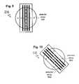
- FIG. 9is a block diagram showing the alignment between an asymmetric subject and the detector of FIG. 8 .
- FIG. 10is a block diagram showing an alternate alignment between an asymmetric subject and the detector of FIG. 8 .
- FIG. 2shows a specific example of this type of enhancement applied to a broadband spectrometer 200 .
- Spectrometer 200includes an illumination source 202 that produces a polychromatic probe beam.
- the probe beampasses through a first lens 204 , first beam splitter 208 and second lens 208 before reaching a subject 210 .
- Subject 210is typically a semiconductor wafer and typically includes an isolated or periodic two or three dimensional surface structure such a line, grating, via or pattern of vias.
- the polychromatic probe beamis reflected by subject 210 and directed through lens 208 , first beam splitter 206 , second beam splitter 212 and third lens 214 before reaching detector 216 .
- lens 208first beam splitter 206
- second beam splitter 212and third lens 214
- detector 216detector 216
- detector 216uses a split configuration. As shown in FIG. 3 the split configuration of detector 216 includes a left half 302 and a right half 304 . Left half 302 and right half 304 operate independently. This allows the separate outputs of the two halves 302 , 304 to be independently analyzed and compared. Light received by the two halves 302 , 304 will be effected by asymmetries in the sample. With an appropriate analysis, (discussed further below), the differences in the signals can be used to extract information about the asymmetries. In this regard, it should be understood that the output signals at both halves may not be the same even for a symmetric sample.
- the subject 210may be aligned to maximize the asymmetry induced differences between left half 302 and right half 304 .
- a modelis generally used to predict the input received by detector 216 .
- the modelis perturbed until the predicted values match the actual input of detector 216 within a desired goodness of fit.
- the modelis based on rigorously coupled wave analysis (RCWA) but other techniques such as boundary integral evaluation may be used.
- RCWArigorously coupled wave analysis
- these modelsare modified to predict the differing inputs received by left half 302 and right half 304 .
- FIGS. 2 and 3describe a case where an existing optical metrology system (a broadband spectrometer) is modified to analyze asymmetric structures. It is important to appreciate that the same technique can be used to modify a range of optical metrology systems including reflectometers and ellipsometers of monochromatic or polychromatic variants. Enhancements of this type are not limited to replacement of existing components (e.g., substitution of split detector 216 for a prior art non-split type). As shown in FIG. 4 , enhancement may also include the addition of components not normally found in existing systems.
- a broadband spectrometer 400includes an illumination source 402 that produces a polychromatic probe beam.
- the probe beampasses through a first lens 404 , first beam splitter 408 and second lens 408 before reaching a subject 410 .
- This particular combination of optical elementsis intended to be representative in nature and other combinations of reflective and refractive optics can be easily substituted.
- Subject 410is typically a semiconductor wafer and typically includes an isolated or periodic two or three dimensional surface structure such a line, grating, via or pattern of vias.
- the polychromatic probe beamis reflected by subject 410 and directed through second lens 408 , first beam splitter 406 , second beam splitter 412 and third lens 414 before reaching first detector 416 .
- First detector 416may be selected from a range of suitable types including the split detector described above and shown in FIGS. 2 and 3 .
- Broadband spectrometer 400includes a fourth lens 418 and a fifth lens 420 to direct a portion of the reflected probe beam to a second detector 422 .
- the light received by second detector 422is created by non-specular reflection of the probe beam.
- the light received by first detector 416is specular reflection.
- information about asymmetriescan be determined.
- first detector 416is implemented using the split detector described previously, information about right and left scattered rays as well as specular and non-specular reflections can be analyzed simultaneously.
- a modeling approach(described above for spectrometer 200 ) is used to predict the inputs received by first detector 416 and second detector 422 .
- the modeling approachis modified to predict the differing inputs received by first detector 416 and second detector 422 .
- the modeling approachmust be further modified to account for right and left scattered rays as well as specular and non-specular reflections.
- Additional sensorsis not limited to broadband spectrometry.
- a range of optical metrology systemsmay be used in combination with this technique including reflectometers and ellipsometers of monochromatic or polychromatic variants.
- a structurally unmodified optical metrology systemis used to analyze asymmetries.
- a broadband spectrometeris used to analyze a subject.
- the subjecte.g., line or grating
- the polarized component of the probe beamis aligned so that its axis of polarization (shown in outline in FIG. 5 ) has an angle of polarization that is greater than normal and less than parallel to the alignment of the structure (e.g. acutely aligned with the asymmetric structure).
- the polarity of the reflected probe beambecomes dependent on the asymmetries of the subject.
- FIG. 6shows another method where a structurally unmodified optical metrology system is used to analyze asymmetries.
- an ellipsometeris used to analyze a subject.
- the subjectthat includes an asymmetric grating.
- a plane perpendicular to the asymmetric gratingis shown for reference.
- the probe beam of the ellipsometerintersects the reference plane at an angle with respect to the plane, to define a non-normal angle of attack.
- the angle of attackis zero—meaning that the probe beam is directed normal to the lines of the grating. This is known as planar diffraction.
- an intermediate angle of attackis used.
- This orientationcreates conical diffraction.
- a typical value for the angle of attackis forty-five degrees. This positions the probe beam midway between the X axis and Y axis, increasing the sensitivity to asymmetry. By measuring the changes in polarity of the reflected probe beam, information about asymmetries can be determined.
- FIG. 7shows another method where a structurally unmodified optical metrology system is used to analyze asymmetries.
- 2 beam profile reflectometry (BPR) system 700is used to analyze a subject.
- BPR system 700includes a laser 702 generating a monochromatic probe beam.
- the probe beam probeis directed by a beam splitter 704 and focused by a lens 706 before reaching a subject 708 .
- Lens 706focuses the relatively wide probe beam into a very small spot on subject 708 .
- subject 708includes an asymmetric structure within the focal point of the probe beam.
- the transition between the wide probe beam and the small spot on subject 708creates a wide range of incident angles.
- the reflected probe beampasses through beam splitter 704 before reaching a detector 710 .
- a processor 712analyzes the output of detector 710 .
- a typical implementation for detector 710includes two linear detector arrays ( 802 and 804 ).
- the detectors arrays 802 , 804are typically oriented perpendicularly to each other to provide coverage in two dimensions.
- the output of detector arrays 802 , 804is typically accessible on an element-by-element basis. Thus, for example, it is possible to access the output of the topmost element of detector array 802 or the leftmost element of detector array 804 .
- Each arraymay be on separate detectors.
- a beam splittercan than be used to divide the reflected beam to land on the two detector arrays.
- a two-dimensional array(such a CCD element) could also be used for more information.
- subject 708is preferably aligned so that one of the detector arrays (either 802 or 804 ) is parallel to the asymmetric structure of the subject.
- the other detector array (either 802 or 804 )is perpendicular to the asymmetric structure with one half of that detector array (either 802 or 804 ) on each side of the asymmetric structure. This is shown for a representative subject in FIG. 9 .
- the separate outputs of the two halves of the straddled detector arrayin this case, the two halves of detector array 804 ) are compared to obtain information about asymmetries.
- a modelis generally used to predict the input received by detector 708 .
- the modelis modified to predict the differing inputs received by the two halves of detector array 804 .
- the parallel/perpendicular alignment shown in FIG. 9may be replaced by an orientation where the line or grating structure is aligned at an acute angle to both detector arrays 802 , 806 .
- FIG. 10an example would be an implementation where the line or grating structure is aligned at a forty-five degree angle to both detector arrays 802 , 804 .
- the analysis hereis similar to the case of parallel/perpendicular alignment except that the outputs of both halves of both detector arrays 802 , 804 are considered.
- a detector array of this typeallows asymmetries to be determined along any axis.
- FIGS. 7 through 10describe a case where a structurally unmodified optical metrology system (a BPR system) is used to analyze asymmetric structures. It is important to appreciate that the same technique can be used to modify a range of optical metrology systems including beam profile ellipsometers (BPE) of monochromatic or polychromatic variants.
- BPR and BPE systemsare described in detail in U.S. Pat. Nos. 4,999,014, 5,042,951, 5,181,080, 5,412,473, 5,596,411, and 6,429,943 as well as U.S. Pat. application Ser. No. 10/243,245, filed Sep. 13, 2002. Each of these documents is incorporated in this document by reference.
- the output signals from the detectors shown in the Figureswill be supplied to a processor (e.g. processor 712 of FIG. 7 ).
- the processorwill analyze the signals based on an algorithm which considers the reflected and scattered light.
- the algorithmsrely on the Fresnel equations.
- the analysiscould be based on various analytical systems including Rigorous Coupled Wave Theory, or bounded or volume integral approaches.
- the reflected output signalsare analyzed to determine the asymmetries in the geometry of the structure. While there are a number of different approaches, most have certain traits in common. More specifically, the analytical approach will typically start with a theoretical “best guess” of the composition and asymmetric geometry of the measured structure. Using Fresnel equations covering both the reflection and scattering of light, calculations are applied to a theoretical model of the structure to determine what the expected measured output signals would be for the theoretical geometry. These theoretical output signals are compared to the actual measured output signals and the differences noted. Based on the differences, the processor will generate a new set of theoretical output signals corresponding to a different theoretical structure. Another comparison is made to determine if the theoretical signals are closer to the actual measured signals. These generation and comparison steps are repeated until the differences between the theoretically generated data and the actually measured data are substantially minimized. Once the differences have been minimized, the theoretical structure corresponding to the best fit theoretical data is assumed to represent the actual structure.
- the minimization routinewill be carried out in real time, associated with the measurements. Since the calculations related to this analysis are very complex, real time calculations can be a challenge. Some approaches for dealing with complex real time calculations are set forth in our co-pending PCT Application WO03/009063 cited above.
- Another approach to dealing with the processing difficultiesis to create a library of solutions prior to the measurement.
- a range of possible structures and their associated theoretical output signalsare generated in advance.
- the resultsare stored as a library in a processor memory.
- the actual measured signalsare compared with sets of theoretically generated output signals stored in the library.
- the structure associated with the set of theoretical signals which most closely matches the actual measured datais assumed to most closely represent the geometry of the measured structure.
- the use of librariesis disclosed in U.S. patent Application 2002/0035455 A1.
- Still another approachis to create a much smaller database of possible solutions. Measured data can then be compared to the database and algorithms are used to interpolate between data points to derive a solution to the geometry of the structure. (See for example, U.S. patent Application 2002/0038196 A1)
- the methods described aboverelate to both CD measurements of asymmetric lines and overlay measurements to distinguish whether overlay displacement is to the right or left of a line.
- the methods described abovealso include any and all possible combinations of SE, BB, BPR and BPE with CD and overlay capability. More specifically, it is known that measurement information from various technologies can be combined to improve the analysis of an unknown sample. Examples of combining measurement technologies are disclosed in some of the above cited references as well as in U.S. Pat. No. 6,278,519 incorporated herein by reference. A combination of information can be relatively simple such as averaging the results from two different measurements. Preferably, all of the measurements are combined and applied to a theoretical model to permit simultaneous regression to an optimal solution.
Landscapes
- Physics & Mathematics (AREA)
- General Physics & Mathematics (AREA)
- Investigating Or Analysing Materials By Optical Means (AREA)
- Length Measuring Devices By Optical Means (AREA)
Abstract
Description
Claims (8)
Priority Applications (1)
| Application Number | Priority Date | Filing Date | Title |
|---|---|---|---|
| US10/385,863US7061627B2 (en) | 2002-03-13 | 2003-03-11 | Optical scatterometry of asymmetric lines and structures |
Applications Claiming Priority (2)
| Application Number | Priority Date | Filing Date | Title |
|---|---|---|---|
| US36415402P | 2002-03-13 | 2002-03-13 | |
| US10/385,863US7061627B2 (en) | 2002-03-13 | 2003-03-11 | Optical scatterometry of asymmetric lines and structures |
Publications (2)
| Publication Number | Publication Date |
|---|---|
| US20050041258A1 US20050041258A1 (en) | 2005-02-24 |
| US7061627B2true US7061627B2 (en) | 2006-06-13 |
Family
ID=34197608
Family Applications (1)
| Application Number | Title | Priority Date | Filing Date |
|---|---|---|---|
| US10/385,863Expired - LifetimeUS7061627B2 (en) | 2002-03-13 | 2003-03-11 | Optical scatterometry of asymmetric lines and structures |
Country Status (1)
| Country | Link |
|---|---|
| US (1) | US7061627B2 (en) |
Cited By (56)
| Publication number | Priority date | Publication date | Assignee | Title |
|---|---|---|---|---|
| US20040233444A1 (en)* | 2003-02-22 | 2004-11-25 | Kla-Tencor Technologies Corporation | Apparatus and methods for detecting overlay errors using scatterometry |
| US20060033921A1 (en)* | 2004-08-16 | 2006-02-16 | Asml Netherlands B.V. | Method and apparatus for angular-resolved spectroscopic lithography characterization |
| US20060126074A1 (en)* | 2004-12-14 | 2006-06-15 | Asml Netherlands B.V. | Inspection apparatus, sample and inspection method |
| US20060139592A1 (en)* | 2004-11-22 | 2006-06-29 | Asml Netherlands B.V. | Latent overlay metrology |
| US20060192936A1 (en)* | 2005-02-25 | 2006-08-31 | Asml Netherlands B.V. | Lithography measurements using scatterometry |
| US20060256324A1 (en)* | 2005-05-10 | 2006-11-16 | Asml Netherlands B.V. | Inspection apparatus and method of inspection |
| US20070002336A1 (en)* | 2005-06-30 | 2007-01-04 | Asml Netherlands B.V. | Metrology apparatus, lithographic apparatus, process apparatus, metrology method and device manufacturing method |
| US20070003840A1 (en)* | 2005-06-30 | 2007-01-04 | Asml Netherlands B.V. | Focus determination method, device manufacturing method, and mask |
| US20070081170A1 (en)* | 2002-07-03 | 2007-04-12 | Tokyo Electron Limited | Overlay metrology method and apparatus using more than one grating per measurement direction |
| US20070093044A1 (en)* | 2005-10-25 | 2007-04-26 | Asml Netherlands B.V. | Method of depositing a metal layer onto a substrate and a method for measuring in three dimensions the topographical features of a substrate |
| US20070153275A1 (en)* | 2005-12-30 | 2007-07-05 | Asml Netherlands B.V. | Optical metrology system and metrology mark characterization device |
| US20070182964A1 (en)* | 2006-02-09 | 2007-08-09 | Asml Netherlands B.V. | Lithographic system, sensor, and method of measuring properties of a substrate |
| US20070201017A1 (en)* | 2006-02-02 | 2007-08-30 | Jon Opsal | High resolution monitoring of CD variations |
| US20070222960A1 (en)* | 2006-03-21 | 2007-09-27 | Asml Netherlands B.V. | Lithographic apparatus and device manufacturing method with reduced scribe lane usage for substrate measurement |
| US20070229785A1 (en)* | 2006-03-28 | 2007-10-04 | Asml Netherlands B.V. | Lithographic apparatus and device manufacturing method using overlay measurement |
| US20070229837A1 (en)* | 2006-03-29 | 2007-10-04 | Asml Netherlands B.V. | Lithographic apparatus and device manufacturing method using overlay measurement quality indication |
| US20070279742A1 (en)* | 2006-05-31 | 2007-12-06 | Asml Netherlands B.V. | Metrology tool, system comprising a lithographic apparatus and a metrology tool, and a method for determining a parameter of a substrate |
| US20070291269A1 (en)* | 2006-06-20 | 2007-12-20 | Asml Netherlands B.V. | Method and apparatus for angular-resolved spectroscopic lithography characterization |
| US20070296960A1 (en)* | 2006-06-13 | 2007-12-27 | Asml Netherlands B.V. | Method of characterising the transmission losses of an optical system |
| US20070296973A1 (en)* | 2006-06-22 | 2007-12-27 | Asml Netherlands B.V. | Method and apparatus for angular-resolved spectroscopic lithography characterization |
| US20080002207A1 (en)* | 2006-06-30 | 2008-01-03 | Asml Netherlands B.V. | Apparatus for angular-resolved spectroscopic lithography characterization and device manufacturing method |
| US20080030701A1 (en)* | 2006-08-03 | 2008-02-07 | Asml Netherlands B.V. | Individual wafer history storage for overlay corrections |
| US20080037134A1 (en)* | 2006-08-10 | 2008-02-14 | Asml Netherlands B.V. | Inspection method and apparatus, lithographic apparatus, lithographic processing cell and device method |
| US20080036984A1 (en)* | 2006-08-08 | 2008-02-14 | Asml Netherlands B.V. | Method and apparatus for angular-resolved spectroscopic lithography characterization |
| US20080043239A1 (en)* | 2006-08-15 | 2008-02-21 | Asml Netherlands B.V. | Method and apparatus for angular-resolved spectroscopic lithography characterization |
| US20080068609A1 (en)* | 2006-09-14 | 2008-03-20 | Asml Netherlands B.V. | Inspection apparatus, an apparatus for projecting an image and a method of measuring a property of a substrate |
| US20080068616A1 (en)* | 2006-09-14 | 2008-03-20 | Asml Netherlands B.V. | Inspection method and apparatus, lithographic apparatus, lithographic processing cell and device manufacturing method |
| US20080069430A1 (en)* | 2006-08-08 | 2008-03-20 | Asml Netherlands B.V. | Method and apparatus for angular-resolved spectroscopic lithography characterization |
| US20080074666A1 (en)* | 2006-09-25 | 2008-03-27 | Asml Netherlands B.V. | Method and apparatus for angular-resolved spectroscopic lithography characterization |
| US20080088854A1 (en)* | 2006-10-13 | 2008-04-17 | Asml Netherlands B.V. | Inspection method and apparatus, lithographic apparatus, lithographic processing cell and device manufacturing method |
| US20080088832A1 (en)* | 2006-10-13 | 2008-04-17 | Asml Netherlands B.V. | Inspection method and apparatus, lithographic apparatus, lithographic processing cell and device manufacturing method |
| US20080117434A1 (en)* | 2006-11-22 | 2008-05-22 | Asml Netherlands B.V. | Inspection method and apparatus, lithographic apparatus, lithographic processing cell and device manufacturing method |
| US20080128644A1 (en)* | 2006-11-30 | 2008-06-05 | Asml Netherlands | Inspection method and apparatus, lithographic apparatus, lithographic processing cell and device manufacturing method |
| US20080137099A1 (en)* | 2006-12-07 | 2008-06-12 | Asml Netherlands B.V. | Inspection method and apparatus, lithographic apparatus, lithographic processing cell and device manufacturing method |
| US20080135774A1 (en)* | 2006-12-08 | 2008-06-12 | Asml Netherlands B.V. | Scatterometer, a lithographic apparatus and a focus analysis method |
| US20080144036A1 (en)* | 2006-12-19 | 2008-06-19 | Asml Netherlands B.V. | Method of measurement, an inspection apparatus and a lithographic apparatus |
| US20080170780A1 (en)* | 2007-01-16 | 2008-07-17 | Asml Netherlands B.V. | Inspection method and apparatus,lithographic apparatus, lithographic processing cell and device manufacturing method |
| US20080174753A1 (en)* | 2007-01-22 | 2008-07-24 | Asml Netherlands B.V. | Method of measurement, an inspection apparatus and a lithographic apparatus |
| US20080198380A1 (en)* | 2007-02-21 | 2008-08-21 | Asml Netherlands B.V. | Inspection method and apparatus, lithographic apparatus, lithographic processing cell and device manufacturing method |
| US20080212097A1 (en)* | 2007-03-01 | 2008-09-04 | Asml Netherlands B.V. | Method of inspection, a method of manufacturing, an inspection apparatus, a substrate, a mask, a lithography apparatus and a lithographic cell |
| US20080239318A1 (en)* | 2007-03-30 | 2008-10-02 | Asml Netherlands B.V. | Method of measuring asymmetry in a scatterometer, a method of measuring an overlay error in a substrate and a metrology apparatus |
| US20080239277A1 (en)* | 2007-03-27 | 2008-10-02 | Asml Netherlands B.V. | Method of forming a substrate for use in calibrating a metrology tool, calibration substrate and metrology tool calibration method |
| US7440105B2 (en) | 2002-12-05 | 2008-10-21 | Kla-Tencor Technologies Corporation | Continuously varying offset mark and methods of determining overlay |
| US20080266560A1 (en)* | 2006-06-30 | 2008-10-30 | Asml Netherlands B.V. | Apparatus for angular-resolved spectroscopic lithography characterization and device manufacturing method |
| US20080279442A1 (en)* | 2007-05-09 | 2008-11-13 | Asml Netherlands B.V. | Inspection method and apparatus, lithographic apparatus, lithographic processing cell and device manufacturing method |
| US7460237B1 (en) | 2007-08-02 | 2008-12-02 | Asml Netherlands B.V. | Inspection method and apparatus, lithographic apparatus, lithographic processing cell and device manufacturing method |
| US20090027691A1 (en)* | 2006-03-21 | 2009-01-29 | Asml Netherlands B.V. | Lithographic Apparatus and Device Manufacturing Method with Reduced Scribe Lane Usage for Substrate Measurement |
| US7570358B2 (en) | 2007-03-30 | 2009-08-04 | Asml Netherlands Bv | Angularly resolved scatterometer, inspection method, lithographic apparatus, lithographic processing cell device manufacturing method and alignment sensor |
| US7599064B2 (en) | 2007-03-07 | 2009-10-06 | Asml Netherlands B.V. | Inspection method and apparatus, lithographic apparatus, lithographic processing cell and device manufacturing method, substrate for use in the methods |
| US7852459B2 (en) | 2007-02-02 | 2010-12-14 | Asml Netherlands B.V. | Inspection method and apparatus, lithographic apparatus, lithographic processing cell and device manufacturing method |
| US7911612B2 (en) | 2007-06-13 | 2011-03-22 | Asml Netherlands B.V. | Inspection method and apparatus, lithographic apparatus, lithographic processing cell and device manufacturing method |
| US7916284B2 (en) | 2006-07-18 | 2011-03-29 | Asml Netherlands B.V. | Inspection method and apparatus, lithographic apparatus, lithographic processing cell and device manufacturing method |
| USRE45245E1 (en) | 2000-08-30 | 2014-11-18 | Kla-Tencor Corporation | Apparatus and methods for determining overlay of structures having rotational or mirror symmetry |
| US20160371423A1 (en)* | 2015-06-22 | 2016-12-22 | Kla-Tencor Corporation | Process-Induced Asymmetry Detection, Quantification, and Control Using Patterned Wafer Geometry Measurements |
| WO2019067375A1 (en)* | 2017-09-27 | 2019-04-04 | Kla-Tencor Corporation | Detection and measurement of dimensions of asymmetric structures |
| US10451412B2 (en) | 2016-04-22 | 2019-10-22 | Kla-Tencor Corporation | Apparatus and methods for detecting overlay errors using scatterometry |
Families Citing this family (5)
| Publication number | Priority date | Publication date | Assignee | Title |
|---|---|---|---|---|
| US7206070B2 (en)* | 2004-11-15 | 2007-04-17 | Therma-Wave, Inc. | Beam profile ellipsometer with rotating compensator |
| US7821643B2 (en)* | 2006-09-06 | 2010-10-26 | Imalux Corporation | Common path systems and methods for frequency domain and time domain optical coherence tomography using non-specular reference reflection and a delivering device for optical radiation with a partially optically transparent non-specular reference reflector |
| US9239522B2 (en)* | 2010-10-08 | 2016-01-19 | Kla-Tencor Corporation | Method of determining an asymmetric property of a structure |
| US20150157199A1 (en)* | 2012-12-06 | 2015-06-11 | Noam Sapiens | Method and apparatus for scatterometric measurement of human tissue |
| KR102086362B1 (en)* | 2013-03-08 | 2020-03-09 | 삼성전자주식회사 | Apparatus of Monitoring a Process Using Poarized Light and Method Thereof |
Citations (25)
| Publication number | Priority date | Publication date | Assignee | Title |
|---|---|---|---|---|
| US4710642A (en) | 1985-08-20 | 1987-12-01 | Mcneil John R | Optical scatterometer having improved sensitivity and bandwidth |
| US4999014A (en)* | 1989-05-04 | 1991-03-12 | Therma-Wave, Inc. | Method and apparatus for measuring thickness of thin films |
| US5042951A (en) | 1989-09-19 | 1991-08-27 | Therma-Wave, Inc. | High resolution ellipsometric apparatus |
| US5159412A (en) | 1991-03-15 | 1992-10-27 | Therma-Wave, Inc. | Optical measurement device with enhanced sensitivity |
| US5166752A (en) | 1990-01-11 | 1992-11-24 | Rudolph Research Corporation | Simultaneous multiple angle/multiple wavelength ellipsometer and method |
| US5181080A (en) | 1991-12-23 | 1993-01-19 | Therma-Wave, Inc. | Method and apparatus for evaluating the thickness of thin films |
| US5264912A (en) | 1992-02-07 | 1993-11-23 | Tencor Instruments | Speckle reduction track filter apparatus for optical inspection of patterned substrates |
| US5412473A (en) | 1993-07-16 | 1995-05-02 | Therma-Wave, Inc. | Multiple angle spectroscopic analyzer utilizing interferometric and ellipsometric devices |
| US5432607A (en) | 1993-02-22 | 1995-07-11 | International Business Machines Corporation | Method and apparatus for inspecting patterned thin films using diffracted beam ellipsometry |
| US5596411A (en) | 1994-10-21 | 1997-01-21 | Therma-Wave, Inc. | Integrated spectroscopic ellipsometer |
| US5739909A (en) | 1995-10-10 | 1998-04-14 | Lucent Technologies Inc. | Measurement and control of linewidths in periodic structures using spectroscopic ellipsometry |
| US5867276A (en) | 1997-03-07 | 1999-02-02 | Bio-Rad Laboratories, Inc. | Method for broad wavelength scatterometry |
| US5867590A (en)* | 1995-01-11 | 1999-02-02 | Nova Measuring Instruments, Ltd. | Method and apparatus for determining a location on a surface of an object |
| US5880838A (en) | 1996-06-05 | 1999-03-09 | California Institute Of California | System and method for optically measuring a structure |
| US5889593A (en)* | 1997-02-26 | 1999-03-30 | Kla Instruments Corporation | Optical system and method for angle-dependent reflection or transmission measurement |
| US5963329A (en) | 1997-10-31 | 1999-10-05 | International Business Machines Corporation | Method and apparatus for measuring the profile of small repeating lines |
| US6081325A (en)* | 1996-06-04 | 2000-06-27 | Kla-Tencor Corporation | Optical scanning system for surface inspection |
| US6268916B1 (en) | 1999-05-11 | 2001-07-31 | Kla-Tencor Corporation | System for non-destructive measurement of samples |
| US6278519B1 (en) | 1998-01-29 | 2001-08-21 | Therma-Wave, Inc. | Apparatus for analyzing multi-layer thin film stacks on semiconductors |
| US6383824B1 (en) | 2001-04-25 | 2002-05-07 | Advanced Micro Devices, Inc. | Method of using scatterometry measurements to control deposition processes |
| US20020080346A1 (en)* | 1997-09-19 | 2002-06-27 | Mehdi Vaez-Iravani | Sample inspection system |
| US20020101585A1 (en) | 1999-03-31 | 2002-08-01 | Norbert Benesch | Apparatus for rapidly measuring angle-dependent diffraction effects on finely patterned surfaces |
| US6429943B1 (en) | 2000-03-29 | 2002-08-06 | Therma-Wave, Inc. | Critical dimension analysis with simultaneous multiple angle of incidence measurements |
| WO2002065545A2 (en) | 2001-02-12 | 2002-08-22 | Sensys Instruments Corporation | Overlay alignment metrology using diffraction gratings |
| US6650422B2 (en) | 2001-03-26 | 2003-11-18 | Advanced Micro Devices, Inc. | Scatterometry techniques to ascertain asymmetry profile of features and generate a feedback or feedforward process control data associated therewith |
- 2003
- 2003-03-11USUS10/385,863patent/US7061627B2/ennot_activeExpired - Lifetime
Patent Citations (25)
| Publication number | Priority date | Publication date | Assignee | Title |
|---|---|---|---|---|
| US4710642A (en) | 1985-08-20 | 1987-12-01 | Mcneil John R | Optical scatterometer having improved sensitivity and bandwidth |
| US4999014A (en)* | 1989-05-04 | 1991-03-12 | Therma-Wave, Inc. | Method and apparatus for measuring thickness of thin films |
| US5042951A (en) | 1989-09-19 | 1991-08-27 | Therma-Wave, Inc. | High resolution ellipsometric apparatus |
| US5166752A (en) | 1990-01-11 | 1992-11-24 | Rudolph Research Corporation | Simultaneous multiple angle/multiple wavelength ellipsometer and method |
| US5159412A (en) | 1991-03-15 | 1992-10-27 | Therma-Wave, Inc. | Optical measurement device with enhanced sensitivity |
| US5181080A (en) | 1991-12-23 | 1993-01-19 | Therma-Wave, Inc. | Method and apparatus for evaluating the thickness of thin films |
| US5264912A (en) | 1992-02-07 | 1993-11-23 | Tencor Instruments | Speckle reduction track filter apparatus for optical inspection of patterned substrates |
| US5432607A (en) | 1993-02-22 | 1995-07-11 | International Business Machines Corporation | Method and apparatus for inspecting patterned thin films using diffracted beam ellipsometry |
| US5412473A (en) | 1993-07-16 | 1995-05-02 | Therma-Wave, Inc. | Multiple angle spectroscopic analyzer utilizing interferometric and ellipsometric devices |
| US5596411A (en) | 1994-10-21 | 1997-01-21 | Therma-Wave, Inc. | Integrated spectroscopic ellipsometer |
| US5867590A (en)* | 1995-01-11 | 1999-02-02 | Nova Measuring Instruments, Ltd. | Method and apparatus for determining a location on a surface of an object |
| US5739909A (en) | 1995-10-10 | 1998-04-14 | Lucent Technologies Inc. | Measurement and control of linewidths in periodic structures using spectroscopic ellipsometry |
| US6081325A (en)* | 1996-06-04 | 2000-06-27 | Kla-Tencor Corporation | Optical scanning system for surface inspection |
| US5880838A (en) | 1996-06-05 | 1999-03-09 | California Institute Of California | System and method for optically measuring a structure |
| US5889593A (en)* | 1997-02-26 | 1999-03-30 | Kla Instruments Corporation | Optical system and method for angle-dependent reflection or transmission measurement |
| US5867276A (en) | 1997-03-07 | 1999-02-02 | Bio-Rad Laboratories, Inc. | Method for broad wavelength scatterometry |
| US20020080346A1 (en)* | 1997-09-19 | 2002-06-27 | Mehdi Vaez-Iravani | Sample inspection system |
| US5963329A (en) | 1997-10-31 | 1999-10-05 | International Business Machines Corporation | Method and apparatus for measuring the profile of small repeating lines |
| US6278519B1 (en) | 1998-01-29 | 2001-08-21 | Therma-Wave, Inc. | Apparatus for analyzing multi-layer thin film stacks on semiconductors |
| US20020101585A1 (en) | 1999-03-31 | 2002-08-01 | Norbert Benesch | Apparatus for rapidly measuring angle-dependent diffraction effects on finely patterned surfaces |
| US6268916B1 (en) | 1999-05-11 | 2001-07-31 | Kla-Tencor Corporation | System for non-destructive measurement of samples |
| US6429943B1 (en) | 2000-03-29 | 2002-08-06 | Therma-Wave, Inc. | Critical dimension analysis with simultaneous multiple angle of incidence measurements |
| WO2002065545A2 (en) | 2001-02-12 | 2002-08-22 | Sensys Instruments Corporation | Overlay alignment metrology using diffraction gratings |
| US6650422B2 (en) | 2001-03-26 | 2003-11-18 | Advanced Micro Devices, Inc. | Scatterometry techniques to ascertain asymmetry profile of features and generate a feedback or feedforward process control data associated therewith |
| US6383824B1 (en) | 2001-04-25 | 2002-05-07 | Advanced Micro Devices, Inc. | Method of using scatterometry measurements to control deposition processes |
Non-Patent Citations (4)
| Title |
|---|
| D.S. Marx et al., "Optical diffraction of focused spots and subwavelength structures," J. Opt. Soc. Am. A, vol. 14, No. 6, Jun. 1997, pp. 1268-1278. |
| D.S. Marx et al., "Polarization quadrature measurement of subwavelength diffracting structures," Applied Optics, vol. 36, No. 25, Sep. 1, 1997, pp. 6434-6440. |
| J. Opsal et al., "Effects of feature edges on thickness readings of thin oxides," SPIE (Process Module Metrology, Control, and Clustering, vol. 1594 (1991), pp. 313-321. |
| X. Wang et al., "Measuring and modeling optical diffraction from subwavelength features," J. Opt. Soc. Am. A, vol. 18, No. 3, Mar. 2001, pp. 565-572. |
Cited By (153)
| Publication number | Priority date | Publication date | Assignee | Title |
|---|---|---|---|---|
| US9702693B2 (en) | 2000-08-30 | 2017-07-11 | Kla-Tencor Corporation | Apparatus for measuring overlay errors |
| US9347879B2 (en) | 2000-08-30 | 2016-05-24 | Kla-Tencor Corporation | Apparatus and methods for detecting overlay errors using scatterometry |
| US9182680B2 (en) | 2000-08-30 | 2015-11-10 | Kla-Tencor Corporation | Apparatus and methods for determining overlay of structures having rotational or mirror symmetry |
| USRE45245E1 (en) | 2000-08-30 | 2014-11-18 | Kla-Tencor Corporation | Apparatus and methods for determining overlay of structures having rotational or mirror symmetry |
| US20070081170A1 (en)* | 2002-07-03 | 2007-04-12 | Tokyo Electron Limited | Overlay metrology method and apparatus using more than one grating per measurement direction |
| US7333200B2 (en)* | 2002-07-03 | 2008-02-19 | Tokyo Electron Limited | Overlay metrology method and apparatus using more than one grating per measurement direction |
| US7317531B2 (en) | 2002-12-05 | 2008-01-08 | Kla-Tencor Technologies Corporation | Apparatus and methods for detecting overlay errors using scatterometry |
| US7564557B2 (en) | 2002-12-05 | 2009-07-21 | Kla-Tencor Technologies Corp. | Apparatus and methods for detecting overlay errors using scatterometry |
| US7440105B2 (en) | 2002-12-05 | 2008-10-21 | Kla-Tencor Technologies Corporation | Continuously varying offset mark and methods of determining overlay |
| US7933016B2 (en) | 2002-12-05 | 2011-04-26 | Kla-Tencor Technologies Corporation | Apparatus and methods for detecting overlay errors using scatterometry |
| US20080049226A1 (en)* | 2002-12-05 | 2008-02-28 | Kla-Tencor Technologies Corporation | Apparatus and methods for detecting overlay errors using scatterometry |
| US7433040B2 (en) | 2002-12-05 | 2008-10-07 | Kla-Tencor Technologies Corp. | Apparatus and methods for detecting overlay errors using scatterometry |
| US7876440B2 (en) | 2002-12-05 | 2011-01-25 | Kla-Tencor Technologies Corporation | Apparatus and methods for detecting overlay errors using scatterometry |
| US20080024766A1 (en)* | 2002-12-05 | 2008-01-31 | Kla-Tencor Technologies Corporation | Apparatus and methods for detecting overlay errors using scatterometry |
| US20080094630A1 (en)* | 2002-12-05 | 2008-04-24 | Kla-Tencor Technologies Corporation | Apparatus and methods for detecting overlay errors using scatterometry |
| US7663753B2 (en) | 2002-12-05 | 2010-02-16 | Kla-Tencor Technologies Corporation | Apparatus and methods for detecting overlay errors using scatterometry |
| US20100091284A1 (en)* | 2002-12-05 | 2010-04-15 | Kla-Tencor Technologies Corporation | Apparatus and methods for detecting overlay errors using scatterometry |
| US7242477B2 (en) | 2003-02-22 | 2007-07-10 | Kla-Tencor Technologies Corporation | Apparatus and methods for detecting overlay errors using scatterometry |
| US20040257571A1 (en)* | 2003-02-22 | 2004-12-23 | Kla-Tencor Technologies Corporation | Apparatus and methods for detecting overlay errors using scatterometry |
| US20040233443A1 (en)* | 2003-02-22 | 2004-11-25 | Kla-Tencor Technologies Corporation | Apparatus and methods for detecting overlay errors using scatterometry |
| US20040233444A1 (en)* | 2003-02-22 | 2004-11-25 | Kla-Tencor Technologies Corporation | Apparatus and methods for detecting overlay errors using scatterometry |
| US7379183B2 (en) | 2003-02-22 | 2008-05-27 | Kla-Tencor Technologies Corp. | Apparatus and methods for detecting overlay errors using scatterometry |
| US7280212B2 (en)* | 2003-02-22 | 2007-10-09 | Kla-Tencor Technologies Corporation | Apparatus and methods for detecting overlay errors using scatterometry |
| US7289213B2 (en) | 2003-02-22 | 2007-10-30 | Kla-Tencor Technologies Corporation | Apparatus and methods for detecting overlay errors using scatterometry |
| US7298481B2 (en) | 2003-02-22 | 2007-11-20 | Kla-Tencor Technologies Corporation | Apparatus and methods for detecting overlay errors using scatterometry |
| US7301634B2 (en)* | 2003-02-22 | 2007-11-27 | Kla-Tencor Technologies Corporation | Apparatus and methods for detecting overlay errors using scatterometry |
| US8760662B2 (en) | 2004-08-16 | 2014-06-24 | Asml Netherlands B.V. | Method and apparatus for angular-resolved spectroscopic lithography characterization |
| US20100277706A1 (en)* | 2004-08-16 | 2010-11-04 | Asml Netherlands B.V. | Method of Measurement, an Inspection Apparatus and a Lithographic Apparatus |
| US8054467B2 (en) | 2004-08-16 | 2011-11-08 | Asml Netherlands B.V. | Method and apparatus for angular-resolved spectroscopic lithography characterization |
| US10955353B2 (en) | 2004-08-16 | 2021-03-23 | Asml Netherlands B.V. | Method and apparatus for angular-resolved spectroscopic lithography characterization |
| US20060066855A1 (en)* | 2004-08-16 | 2006-03-30 | Asml Netherlands B.V. | Method and apparatus for angular-resolved spectroscopic lithography characterization |
| US20060033921A1 (en)* | 2004-08-16 | 2006-02-16 | Asml Netherlands B.V. | Method and apparatus for angular-resolved spectroscopic lithography characterization |
| US11525786B2 (en) | 2004-08-16 | 2022-12-13 | Asml Netherlands B.V. | Method and apparatus for angular-resolved spectroscopic lithography characterization |
| US10241055B2 (en) | 2004-08-16 | 2019-03-26 | Asml Netherlands B.V. | Method and apparatus for angular-resolved spectroscopic lithography characterization |
| US8553230B2 (en) | 2004-08-16 | 2013-10-08 | Asml Netherlands B.V. | Method and apparatus for angular-resolved spectroscopic lithography characterization |
| US7791732B2 (en) | 2004-08-16 | 2010-09-07 | Asml Netherlands B.V. | Method and apparatus for angular-resolved spectroscopic lithography characterization |
| US20110007314A1 (en)* | 2004-08-16 | 2011-01-13 | Asml Netherlands B.V. | Method and apparatus for angular-resolved spectroscopic lithography characterization |
| US8111398B2 (en) | 2004-08-16 | 2012-02-07 | Asml Netherlands B.V. | Method of measurement, an inspection apparatus and a lithographic apparatus |
| US7791727B2 (en)* | 2004-08-16 | 2010-09-07 | Asml Netherlands B.V. | Method and apparatus for angular-resolved spectroscopic lithography characterization |
| US20060139592A1 (en)* | 2004-11-22 | 2006-06-29 | Asml Netherlands B.V. | Latent overlay metrology |
| US7453577B2 (en) | 2004-12-14 | 2008-11-18 | Asml Netherlands B.V. | Apparatus and method for inspecting a patterned part of a sample |
| US20060126074A1 (en)* | 2004-12-14 | 2006-06-15 | Asml Netherlands B.V. | Inspection apparatus, sample and inspection method |
| US7443486B2 (en) | 2005-02-25 | 2008-10-28 | Asml Netherlands B.V. | Method for predicting a critical dimension of a feature imaged by a lithographic apparatus |
| US20060192936A1 (en)* | 2005-02-25 | 2006-08-31 | Asml Netherlands B.V. | Lithography measurements using scatterometry |
| US7315384B2 (en) | 2005-05-10 | 2008-01-01 | Asml Netherlands B.V. | Inspection apparatus and method of inspection |
| US20060256324A1 (en)* | 2005-05-10 | 2006-11-16 | Asml Netherlands B.V. | Inspection apparatus and method of inspection |
| US20070013921A1 (en)* | 2005-06-30 | 2007-01-18 | Asml Netherlands B.V. | Metrology apparatus, lithographic apparatus, process apparatus metrology method and device manufacturing method |
| US20070003840A1 (en)* | 2005-06-30 | 2007-01-04 | Asml Netherlands B.V. | Focus determination method, device manufacturing method, and mask |
| US20070002336A1 (en)* | 2005-06-30 | 2007-01-04 | Asml Netherlands B.V. | Metrology apparatus, lithographic apparatus, process apparatus, metrology method and device manufacturing method |
| US7532307B2 (en) | 2005-06-30 | 2009-05-12 | Asml Netherlands B.V. | Focus determination method, device manufacturing method, and mask |
| US7403293B2 (en) | 2005-06-30 | 2008-07-22 | Asml Netherlands | Metrology apparatus, lithographic apparatus, process apparatus metrology method and device manufacturing method |
| US20070093044A1 (en)* | 2005-10-25 | 2007-04-26 | Asml Netherlands B.V. | Method of depositing a metal layer onto a substrate and a method for measuring in three dimensions the topographical features of a substrate |
| US20070153274A1 (en)* | 2005-12-30 | 2007-07-05 | Asml Netherlands B.V. | Optical metrology system and metrology mark characterization device |
| US7649636B2 (en) | 2005-12-30 | 2010-01-19 | Asml Netherlands B.V. | Optical metrology system and metrology mark characterization device |
| US20070153275A1 (en)* | 2005-12-30 | 2007-07-05 | Asml Netherlands B.V. | Optical metrology system and metrology mark characterization device |
| US7933026B2 (en) | 2006-02-02 | 2011-04-26 | Kla-Tencor Corporation | High resolution monitoring of CD variations |
| US20090259605A1 (en)* | 2006-02-02 | 2009-10-15 | Kla Tencor Corporation | High resolution monitoring of cd variations |
| US7567351B2 (en) | 2006-02-02 | 2009-07-28 | Kla-Tencor Corporation | High resolution monitoring of CD variations |
| US20070201017A1 (en)* | 2006-02-02 | 2007-08-30 | Jon Opsal | High resolution monitoring of CD variations |
| US20110205554A1 (en)* | 2006-02-02 | 2011-08-25 | Kla-Tencor Corporation | High resolution monitoring of cd variations |
| US8049903B2 (en) | 2006-02-02 | 2011-11-01 | Kla-Tencor Corporation | High resolution monitoring of CD variations |
| US20070182964A1 (en)* | 2006-02-09 | 2007-08-09 | Asml Netherlands B.V. | Lithographic system, sensor, and method of measuring properties of a substrate |
| US7480050B2 (en) | 2006-02-09 | 2009-01-20 | Asml Netherlands B.V. | Lithographic system, sensor, and method of measuring properties of a substrate |
| US7821650B2 (en) | 2006-03-21 | 2010-10-26 | Asml Netherlands B.V. | Lithographic apparatus and device manufacturing method with reduced scribe lane usage for substrate measurement |
| US20070222960A1 (en)* | 2006-03-21 | 2007-09-27 | Asml Netherlands B.V. | Lithographic apparatus and device manufacturing method with reduced scribe lane usage for substrate measurement |
| US20090027691A1 (en)* | 2006-03-21 | 2009-01-29 | Asml Netherlands B.V. | Lithographic Apparatus and Device Manufacturing Method with Reduced Scribe Lane Usage for Substrate Measurement |
| US7486408B2 (en) | 2006-03-21 | 2009-02-03 | Asml Netherlands B.V. | Lithographic apparatus and device manufacturing method with reduced scribe lane usage for substrate measurement |
| US8264686B2 (en) | 2006-03-28 | 2012-09-11 | Asml Netherlands B.V. | Lithographic apparatus and device manufacturing method using overlay measurement |
| US20090244538A1 (en)* | 2006-03-28 | 2009-10-01 | Asml Netherlands B.V. | Lithographic Apparatus and Device Manufacturing Method Using Overlay Measurement |
| US20070229785A1 (en)* | 2006-03-28 | 2007-10-04 | Asml Netherlands B.V. | Lithographic apparatus and device manufacturing method using overlay measurement |
| US7532305B2 (en) | 2006-03-28 | 2009-05-12 | Asml Netherlands B.V. | Lithographic apparatus and device manufacturing method using overlay measurement |
| US7391513B2 (en) | 2006-03-29 | 2008-06-24 | Asml Netherlands B.V. | Lithographic apparatus and device manufacturing method using overlay measurement quality indication |
| US20070229837A1 (en)* | 2006-03-29 | 2007-10-04 | Asml Netherlands B.V. | Lithographic apparatus and device manufacturing method using overlay measurement quality indication |
| US20070279742A1 (en)* | 2006-05-31 | 2007-12-06 | Asml Netherlands B.V. | Metrology tool, system comprising a lithographic apparatus and a metrology tool, and a method for determining a parameter of a substrate |
| US7586598B2 (en) | 2006-05-31 | 2009-09-08 | Asml Netherlands B.V. | Metrology tool, system comprising a lithographic apparatus and a metrology tool, and a method for determining a parameter of a substrate |
| US7961309B2 (en) | 2006-05-31 | 2011-06-14 | Asml Netherlands B.V. | Metrology tool, system comprising a lithographic apparatus and a metrology tool, and a method for determining a parameter of a substrate |
| US20070279644A1 (en)* | 2006-05-31 | 2007-12-06 | Asml Netherlands B.V. | Metrology tool, system comprising a lithographic apparatus and a metrology tool, and a method for determining a parameter of a substrate |
| US20090296081A1 (en)* | 2006-05-31 | 2009-12-03 | Asml Netherlands B. V. | Metrology Tool, System Comprising a Lithographic Apparatus and a Metrology Tool, and a Method for Determining a Parameter of a Substrate |
| US7502103B2 (en) | 2006-05-31 | 2009-03-10 | Asml Netherlands B.V. | Metrology tool, system comprising a lithographic apparatus and a metrology tool, and a method for determining a parameter of a substrate |
| US7791724B2 (en) | 2006-06-13 | 2010-09-07 | Asml Netherlands B.V. | Characterization of transmission losses in an optical system |
| US20070296960A1 (en)* | 2006-06-13 | 2007-12-27 | Asml Netherlands B.V. | Method of characterising the transmission losses of an optical system |
| US7898662B2 (en) | 2006-06-20 | 2011-03-01 | Asml Netherlands B.V. | Method and apparatus for angular-resolved spectroscopic lithography characterization |
| US8064056B2 (en) | 2006-06-20 | 2011-11-22 | Asml Netherlands B.V. | Substrate used in a method and apparatus for angular-resolved spectroscopic lithography characterization |
| US20110122496A1 (en)* | 2006-06-20 | 2011-05-26 | Asml Netherlands B.V. | Substrate Used in a Method and Apparatus for Angular-Resolved Spectroscopic Lithography Characterization |
| US20070291269A1 (en)* | 2006-06-20 | 2007-12-20 | Asml Netherlands B.V. | Method and apparatus for angular-resolved spectroscopic lithography characterization |
| US7692792B2 (en) | 2006-06-22 | 2010-04-06 | Asml Netherlands B.V. | Method and apparatus for angular-resolved spectroscopic lithography characterization |
| US20070296973A1 (en)* | 2006-06-22 | 2007-12-27 | Asml Netherlands B.V. | Method and apparatus for angular-resolved spectroscopic lithography characterization |
| US20080002207A1 (en)* | 2006-06-30 | 2008-01-03 | Asml Netherlands B.V. | Apparatus for angular-resolved spectroscopic lithography characterization and device manufacturing method |
| US7999940B2 (en) | 2006-06-30 | 2011-08-16 | Asml Netherlands B.V. | Apparatus for angular-resolved spectroscopic lithography characterization |
| US7999943B2 (en) | 2006-06-30 | 2011-08-16 | Asml Netherlands B.V. | Device manufacturing method with angular-resolved spectroscopic lithography characterization |
| US7659988B2 (en) | 2006-06-30 | 2010-02-09 | Asml Netherlands B.V. | Apparatus for angular-resolved spectroscopic lithography characterization and device manufacturing method |
| US20080266560A1 (en)* | 2006-06-30 | 2008-10-30 | Asml Netherlands B.V. | Apparatus for angular-resolved spectroscopic lithography characterization and device manufacturing method |
| US7916284B2 (en) | 2006-07-18 | 2011-03-29 | Asml Netherlands B.V. | Inspection method and apparatus, lithographic apparatus, lithographic processing cell and device manufacturing method |
| US7808613B2 (en) | 2006-08-03 | 2010-10-05 | Asml Netherlands B.V. | Individual wafer history storage for overlay corrections |
| US20080030701A1 (en)* | 2006-08-03 | 2008-02-07 | Asml Netherlands B.V. | Individual wafer history storage for overlay corrections |
| US7643666B2 (en) | 2006-08-08 | 2010-01-05 | Asml Netherlands B.V. | Method and apparatus for angular-resolved spectroscopic lithography characterization |
| US20080036984A1 (en)* | 2006-08-08 | 2008-02-14 | Asml Netherlands B.V. | Method and apparatus for angular-resolved spectroscopic lithography characterization |
| US20080069430A1 (en)* | 2006-08-08 | 2008-03-20 | Asml Netherlands B.V. | Method and apparatus for angular-resolved spectroscopic lithography characterization |
| US20090294635A1 (en)* | 2006-08-10 | 2009-12-03 | Asml Netherlands B.V. | Inspection Method and Apparatus, Lithographic Apparatus, Lithographic Processing Cell and Device Manufacturing Method |
| US8120001B2 (en) | 2006-08-10 | 2012-02-21 | Asml Netherlands B.V. | Inspection method and apparatus, lithographic apparatus, lithographic processing cell and device manufacturing method |
| US20080037134A1 (en)* | 2006-08-10 | 2008-02-14 | Asml Netherlands B.V. | Inspection method and apparatus, lithographic apparatus, lithographic processing cell and device method |
| US7589832B2 (en) | 2006-08-10 | 2009-09-15 | Asml Netherlands B.V. | Inspection method and apparatus, lithographic apparatus, lithographic processing cell and device method |
| US7564555B2 (en) | 2006-08-15 | 2009-07-21 | Asml Netherlands B.V. | Method and apparatus for angular-resolved spectroscopic lithography characterization |
| US20080043239A1 (en)* | 2006-08-15 | 2008-02-21 | Asml Netherlands B.V. | Method and apparatus for angular-resolved spectroscopic lithography characterization |
| US7532331B2 (en) | 2006-09-14 | 2009-05-12 | Asml Netherlands B.V. | Inspection method and apparatus, lithographic apparatus, lithographic processing cell and device manufacturing method |
| US7969577B2 (en) | 2006-09-14 | 2011-06-28 | Asml Netherlands B.V. | Inspection apparatus, an apparatus for projecting an image and a method of measuring a property of a substrate |
| US7715019B2 (en) | 2006-09-14 | 2010-05-11 | Asml Netherlands B.V. | Inspection method and apparatus, lithographic apparatus, lithographic processing cell and device manufacturing method |
| US20080068616A1 (en)* | 2006-09-14 | 2008-03-20 | Asml Netherlands B.V. | Inspection method and apparatus, lithographic apparatus, lithographic processing cell and device manufacturing method |
| US20080068609A1 (en)* | 2006-09-14 | 2008-03-20 | Asml Netherlands B.V. | Inspection apparatus, an apparatus for projecting an image and a method of measuring a property of a substrate |
| US20080074666A1 (en)* | 2006-09-25 | 2008-03-27 | Asml Netherlands B.V. | Method and apparatus for angular-resolved spectroscopic lithography characterization |
| US7573584B2 (en) | 2006-09-25 | 2009-08-11 | Asml Netherlands B.V. | Method and apparatus for angular-resolved spectroscopic lithography characterization |
| US20080088832A1 (en)* | 2006-10-13 | 2008-04-17 | Asml Netherlands B.V. | Inspection method and apparatus, lithographic apparatus, lithographic processing cell and device manufacturing method |
| US8294907B2 (en) | 2006-10-13 | 2012-10-23 | Asml Netherlands B.V. | Inspection method and apparatus, lithographic apparatus, lithographic processing cell and device manufacturing method |
| US8233155B2 (en) | 2006-10-13 | 2012-07-31 | Asml Netherlands B.V. | Inspection method and apparatus, lithographic apparatus, lithographic processing cell and device manufacturing method |
| US20080088854A1 (en)* | 2006-10-13 | 2008-04-17 | Asml Netherlands B.V. | Inspection method and apparatus, lithographic apparatus, lithographic processing cell and device manufacturing method |
| US20080117434A1 (en)* | 2006-11-22 | 2008-05-22 | Asml Netherlands B.V. | Inspection method and apparatus, lithographic apparatus, lithographic processing cell and device manufacturing method |
| US7630087B2 (en) | 2006-11-22 | 2009-12-08 | Asml Netherlands B.V. | Inspection method and apparatus, lithographic apparatus, lithographic processing cell and device manufacturing method |
| US20080128644A1 (en)* | 2006-11-30 | 2008-06-05 | Asml Netherlands | Inspection method and apparatus, lithographic apparatus, lithographic processing cell and device manufacturing method |
| US7710572B2 (en) | 2006-11-30 | 2010-05-04 | Asml Netherlands B.V. | Inspection method and apparatus, lithographic apparatus, lithographic processing cell and device manufacturing method |
| US20080137099A1 (en)* | 2006-12-07 | 2008-06-12 | Asml Netherlands B.V. | Inspection method and apparatus, lithographic apparatus, lithographic processing cell and device manufacturing method |
| US7557934B2 (en) | 2006-12-07 | 2009-07-07 | Asml Netherlands B.V. | Inspection method and apparatus, lithographic apparatus, lithographic processing cell and device manufacturing method |
| US20080135774A1 (en)* | 2006-12-08 | 2008-06-12 | Asml Netherlands B.V. | Scatterometer, a lithographic apparatus and a focus analysis method |
| US7630070B2 (en) | 2006-12-08 | 2009-12-08 | Asml Netherlands B.V. | Scatterometer, a lithographic apparatus and a focus analysis method |
| US20080151228A1 (en)* | 2006-12-08 | 2008-06-26 | Asml Netherlands B.V. | Scatterometer, a lithographic apparatus and a focus analysis method |
| US20080144036A1 (en)* | 2006-12-19 | 2008-06-19 | Asml Netherlands B.V. | Method of measurement, an inspection apparatus and a lithographic apparatus |
| US7916927B2 (en) | 2007-01-16 | 2011-03-29 | Asml Netherlands B.V. | Inspection method and apparatus, lithographic apparatus, lithographic processing cell and device manufacturing method |
| US20080170780A1 (en)* | 2007-01-16 | 2008-07-17 | Asml Netherlands B.V. | Inspection method and apparatus,lithographic apparatus, lithographic processing cell and device manufacturing method |
| US7619737B2 (en) | 2007-01-22 | 2009-11-17 | Asml Netherlands B.V | Method of measurement, an inspection apparatus and a lithographic apparatus |
| US20080174753A1 (en)* | 2007-01-22 | 2008-07-24 | Asml Netherlands B.V. | Method of measurement, an inspection apparatus and a lithographic apparatus |
| US7852459B2 (en) | 2007-02-02 | 2010-12-14 | Asml Netherlands B.V. | Inspection method and apparatus, lithographic apparatus, lithographic processing cell and device manufacturing method |
| US7839506B2 (en) | 2007-02-21 | 2010-11-23 | Asml Netherlands B.V. | Inspection method and apparatus, lithographic apparatus, lithographic processing cell and device manufacturing method |
| US20080198380A1 (en)* | 2007-02-21 | 2008-08-21 | Asml Netherlands B.V. | Inspection method and apparatus, lithographic apparatus, lithographic processing cell and device manufacturing method |
| US7701577B2 (en) | 2007-02-21 | 2010-04-20 | Asml Netherlands B.V. | Inspection method and apparatus, lithographic apparatus, lithographic processing cell and device manufacturing method |
| US20100157299A1 (en)* | 2007-02-21 | 2010-06-24 | Asml Netherlands B.V. | Inspection Method and Apparatus, Lithographic Apparatus, Lithographic Processing Cell and Device Manufacturing Method |
| US20080212097A1 (en)* | 2007-03-01 | 2008-09-04 | Asml Netherlands B.V. | Method of inspection, a method of manufacturing, an inspection apparatus, a substrate, a mask, a lithography apparatus and a lithographic cell |
| US7724370B2 (en) | 2007-03-01 | 2010-05-25 | Asml Netherlands B.V. | Method of inspection, a method of manufacturing, an inspection apparatus, a substrate, a mask, a lithography apparatus and a lithographic cell |
| US7599064B2 (en) | 2007-03-07 | 2009-10-06 | Asml Netherlands B.V. | Inspection method and apparatus, lithographic apparatus, lithographic processing cell and device manufacturing method, substrate for use in the methods |
| US7605907B2 (en) | 2007-03-27 | 2009-10-20 | Asml Netherlands B.V. | Method of forming a substrate for use in calibrating a metrology tool, calibration substrate and metrology tool calibration method |
| US20080239277A1 (en)* | 2007-03-27 | 2008-10-02 | Asml Netherlands B.V. | Method of forming a substrate for use in calibrating a metrology tool, calibration substrate and metrology tool calibration method |
| US8031337B2 (en) | 2007-03-30 | 2011-10-04 | Asml Netherlands B.V. | Angularly resolved scatterometer |
| US20080239318A1 (en)* | 2007-03-30 | 2008-10-02 | Asml Netherlands B.V. | Method of measuring asymmetry in a scatterometer, a method of measuring an overlay error in a substrate and a metrology apparatus |
| US7656518B2 (en) | 2007-03-30 | 2010-02-02 | Asml Netherlands B.V. | Method of measuring asymmetry in a scatterometer, a method of measuring an overlay error in a substrate and a metrology apparatus |
| US20090262366A1 (en)* | 2007-03-30 | 2009-10-22 | Asml Netherlands B.V. | Angularly Resolved Scatterometer |
| US7570358B2 (en) | 2007-03-30 | 2009-08-04 | Asml Netherlands Bv | Angularly resolved scatterometer, inspection method, lithographic apparatus, lithographic processing cell device manufacturing method and alignment sensor |
| US8189195B2 (en) | 2007-05-09 | 2012-05-29 | Asml Netherlands B.V. | Inspection method and apparatus, lithographic apparatus, lithographic processing cell and device manufacturing method |
| US20080279442A1 (en)* | 2007-05-09 | 2008-11-13 | Asml Netherlands B.V. | Inspection method and apparatus, lithographic apparatus, lithographic processing cell and device manufacturing method |
| US7911612B2 (en) | 2007-06-13 | 2011-03-22 | Asml Netherlands B.V. | Inspection method and apparatus, lithographic apparatus, lithographic processing cell and device manufacturing method |
| US7460237B1 (en) | 2007-08-02 | 2008-12-02 | Asml Netherlands B.V. | Inspection method and apparatus, lithographic apparatus, lithographic processing cell and device manufacturing method |
| US9779202B2 (en)* | 2015-06-22 | 2017-10-03 | Kla-Tencor Corporation | Process-induced asymmetry detection, quantification, and control using patterned wafer geometry measurements |
| US20160371423A1 (en)* | 2015-06-22 | 2016-12-22 | Kla-Tencor Corporation | Process-Induced Asymmetry Detection, Quantification, and Control Using Patterned Wafer Geometry Measurements |
| US10451412B2 (en) | 2016-04-22 | 2019-10-22 | Kla-Tencor Corporation | Apparatus and methods for detecting overlay errors using scatterometry |
| WO2019067375A1 (en)* | 2017-09-27 | 2019-04-04 | Kla-Tencor Corporation | Detection and measurement of dimensions of asymmetric structures |
| US10732515B2 (en) | 2017-09-27 | 2020-08-04 | Kla-Tencor Corporation | Detection and measurement of dimensions of asymmetric structures |
Also Published As
| Publication number | Publication date |
|---|---|
| US20050041258A1 (en) | 2005-02-24 |
Similar Documents
| Publication | Publication Date | Title |
|---|---|---|
| US7061627B2 (en) | Optical scatterometry of asymmetric lines and structures | |
| US6829057B2 (en) | Critical dimension analysis with simultaneous multiple angle of incidence measurements | |
| US7511293B2 (en) | Scatterometer having a computer system that reads data from selected pixels of the sensor array | |
| US6842259B2 (en) | Analysis of isolated and aperiodic structures with simultaneous multiple angle of incidence measurements | |
| US7271921B2 (en) | Method and apparatus for determining surface layer thickness using continuous multi-wavelength surface scanning | |
| TWI721993B (en) | Methods and apparatus for measuring height on a semiconductor wafer | |
| US7046376B2 (en) | Overlay targets with isolated, critical-dimension features and apparatus to measure overlay | |
| US7483133B2 (en) | Multiple angle of incidence spectroscopic scatterometer system | |
| US20050046855A1 (en) | Interference scatterometer | |
| US8045179B1 (en) | Bright and dark field scatterometry systems for line roughness metrology | |
| US9243886B1 (en) | Optical metrology of periodic targets in presence of multiple diffraction orders | |
| US7202958B1 (en) | Modeling a sample with an underlying complicated structure |
Legal Events
| Date | Code | Title | Description |
|---|---|---|---|
| AS | Assignment | Owner name:THERMA-WAVE, INC., CALIFORNIA Free format text:ASSIGNMENT OF ASSIGNORS INTEREST;ASSIGNOR:OPSAL, JON;REEL/FRAME:014207/0069 Effective date:20030314 | |
| AS | Assignment | Owner name:THERMA-WAVE, INC., CALIFORNIA Free format text:NOTICE OF OWNERSHIP INTEREST;ASSIGNOR:ROSENCWAIG, ALLAN;REEL/FRAME:015823/0202 Effective date:20040227 | |
| STCF | Information on status: patent grant | Free format text:PATENTED CASE | |
| FEPP | Fee payment procedure | Free format text:PAT HOLDER NO LONGER CLAIMS SMALL ENTITY STATUS, ENTITY STATUS SET TO UNDISCOUNTED (ORIGINAL EVENT CODE: STOL); ENTITY STATUS OF PATENT OWNER: LARGE ENTITY | |
| AS | Assignment | Owner name:KLA-TENCOR CORP., CALIFORNIA Free format text:ASSIGNMENT OF ASSIGNORS INTEREST;ASSIGNOR:ROSENCWAIG, ALLAN;REEL/FRAME:021328/0663 Effective date:20080513 | |
| FPAY | Fee payment | Year of fee payment:4 | |
| FPAY | Fee payment | Year of fee payment:8 | |
| MAFP | Maintenance fee payment | Free format text:PAYMENT OF MAINTENANCE FEE, 12TH YEAR, LARGE ENTITY (ORIGINAL EVENT CODE: M1553) Year of fee payment:12 |