US7060601B2 - Packaging substrates for integrated circuits and soldering methods - Google Patents
Packaging substrates for integrated circuits and soldering methodsDownload PDFInfo
- Publication number
- US7060601B2 US7060601B2US10/739,707US73970703AUS7060601B2US 7060601 B2US7060601 B2US 7060601B2US 73970703 AUS73970703 AUS 73970703AUS 7060601 B2US7060601 B2US 7060601B2
- Authority
- US
- United States
- Prior art keywords
- solder
- interposer
- substrate
- contact pads
- melting temperature
- Prior art date
- Legal status (The legal status is an assumption and is not a legal conclusion. Google has not performed a legal analysis and makes no representation as to the accuracy of the status listed.)
- Expired - Lifetime
Links
Images


Classifications
- H—ELECTRICITY
- H01—ELECTRIC ELEMENTS
- H01L—SEMICONDUCTOR DEVICES NOT COVERED BY CLASS H10
- H01L23/00—Details of semiconductor or other solid state devices
- H01L23/12—Mountings, e.g. non-detachable insulating substrates
- H01L23/14—Mountings, e.g. non-detachable insulating substrates characterised by the material or its electrical properties
- H01L23/147—Semiconductor insulating substrates
- H—ELECTRICITY
- H01—ELECTRIC ELEMENTS
- H01L—SEMICONDUCTOR DEVICES NOT COVERED BY CLASS H10
- H01L23/00—Details of semiconductor or other solid state devices
- H01L23/48—Arrangements for conducting electric current to or from the solid state body in operation, e.g. leads, terminal arrangements ; Selection of materials therefor
- H01L23/481—Internal lead connections, e.g. via connections, feedthrough structures
- H—ELECTRICITY
- H01—ELECTRIC ELEMENTS
- H01L—SEMICONDUCTOR DEVICES NOT COVERED BY CLASS H10
- H01L23/00—Details of semiconductor or other solid state devices
- H01L23/48—Arrangements for conducting electric current to or from the solid state body in operation, e.g. leads, terminal arrangements ; Selection of materials therefor
- H01L23/488—Arrangements for conducting electric current to or from the solid state body in operation, e.g. leads, terminal arrangements ; Selection of materials therefor consisting of soldered or bonded constructions
- H01L23/498—Leads, i.e. metallisations or lead-frames on insulating substrates, e.g. chip carriers
- H01L23/49827—Via connections through the substrates, e.g. pins going through the substrate, coaxial cables
- H—ELECTRICITY
- H01—ELECTRIC ELEMENTS
- H01L—SEMICONDUCTOR DEVICES NOT COVERED BY CLASS H10
- H01L23/00—Details of semiconductor or other solid state devices
- H01L23/52—Arrangements for conducting electric current within the device in operation from one component to another, i.e. interconnections, e.g. wires, lead frames
- H01L23/538—Arrangements for conducting electric current within the device in operation from one component to another, i.e. interconnections, e.g. wires, lead frames the interconnection structure between a plurality of semiconductor chips being formed on, or in, insulating substrates
- H01L23/5384—Conductive vias through the substrate with or without pins, e.g. buried coaxial conductors
- H—ELECTRICITY
- H01—ELECTRIC ELEMENTS
- H01L—SEMICONDUCTOR DEVICES NOT COVERED BY CLASS H10
- H01L23/00—Details of semiconductor or other solid state devices
- H01L23/52—Arrangements for conducting electric current within the device in operation from one component to another, i.e. interconnections, e.g. wires, lead frames
- H01L23/538—Arrangements for conducting electric current within the device in operation from one component to another, i.e. interconnections, e.g. wires, lead frames the interconnection structure between a plurality of semiconductor chips being formed on, or in, insulating substrates
- H01L23/5385—Assembly of a plurality of insulating substrates
- H—ELECTRICITY
- H01—ELECTRIC ELEMENTS
- H01L—SEMICONDUCTOR DEVICES NOT COVERED BY CLASS H10
- H01L25/00—Assemblies consisting of a plurality of semiconductor or other solid state devices
- H01L25/03—Assemblies consisting of a plurality of semiconductor or other solid state devices all the devices being of a type provided for in a single subclass of subclasses H10B, H10D, H10F, H10H, H10K or H10N, e.g. assemblies of rectifier diodes
- H01L25/04—Assemblies consisting of a plurality of semiconductor or other solid state devices all the devices being of a type provided for in a single subclass of subclasses H10B, H10D, H10F, H10H, H10K or H10N, e.g. assemblies of rectifier diodes the devices not having separate containers
- H01L25/065—Assemblies consisting of a plurality of semiconductor or other solid state devices all the devices being of a type provided for in a single subclass of subclasses H10B, H10D, H10F, H10H, H10K or H10N, e.g. assemblies of rectifier diodes the devices not having separate containers the devices being of a type provided for in group H10D89/00
- H01L25/0655—Assemblies consisting of a plurality of semiconductor or other solid state devices all the devices being of a type provided for in a single subclass of subclasses H10B, H10D, H10F, H10H, H10K or H10N, e.g. assemblies of rectifier diodes the devices not having separate containers the devices being of a type provided for in group H10D89/00 the devices being arranged next to each other
- H—ELECTRICITY
- H01—ELECTRIC ELEMENTS
- H01L—SEMICONDUCTOR DEVICES NOT COVERED BY CLASS H10
- H01L2224/00—Indexing scheme for arrangements for connecting or disconnecting semiconductor or solid-state bodies and methods related thereto as covered by H01L24/00
- H01L2224/01—Means for bonding being attached to, or being formed on, the surface to be connected, e.g. chip-to-package, die-attach, "first-level" interconnects; Manufacturing methods related thereto
- H01L2224/42—Wire connectors; Manufacturing methods related thereto
- H01L2224/47—Structure, shape, material or disposition of the wire connectors after the connecting process
- H01L2224/48—Structure, shape, material or disposition of the wire connectors after the connecting process of an individual wire connector
- H01L2224/481—Disposition
- H01L2224/48151—Connecting between a semiconductor or solid-state body and an item not being a semiconductor or solid-state body, e.g. chip-to-substrate, chip-to-passive
- H01L2224/48221—Connecting between a semiconductor or solid-state body and an item not being a semiconductor or solid-state body, e.g. chip-to-substrate, chip-to-passive the body and the item being stacked
- H01L2224/48225—Connecting between a semiconductor or solid-state body and an item not being a semiconductor or solid-state body, e.g. chip-to-substrate, chip-to-passive the body and the item being stacked the item being non-metallic, e.g. insulating substrate with or without metallisation
- H01L2224/48227—Connecting between a semiconductor or solid-state body and an item not being a semiconductor or solid-state body, e.g. chip-to-substrate, chip-to-passive the body and the item being stacked the item being non-metallic, e.g. insulating substrate with or without metallisation connecting the wire to a bond pad of the item
- H—ELECTRICITY
- H01—ELECTRIC ELEMENTS
- H01L—SEMICONDUCTOR DEVICES NOT COVERED BY CLASS H10
- H01L2224/00—Indexing scheme for arrangements for connecting or disconnecting semiconductor or solid-state bodies and methods related thereto as covered by H01L24/00
- H01L2224/73—Means for bonding being of different types provided for in two or more of groups H01L2224/10, H01L2224/18, H01L2224/26, H01L2224/34, H01L2224/42, H01L2224/50, H01L2224/63, H01L2224/71
- H01L2224/732—Location after the connecting process
- H01L2224/73251—Location after the connecting process on different surfaces
- H01L2224/73257—Bump and wire connectors
- H—ELECTRICITY
- H01—ELECTRIC ELEMENTS
- H01L—SEMICONDUCTOR DEVICES NOT COVERED BY CLASS H10
- H01L2224/00—Indexing scheme for arrangements for connecting or disconnecting semiconductor or solid-state bodies and methods related thereto as covered by H01L24/00
- H01L2224/80—Methods for connecting semiconductor or other solid state bodies using means for bonding being attached to, or being formed on, the surface to be connected
- H01L2224/81—Methods for connecting semiconductor or other solid state bodies using means for bonding being attached to, or being formed on, the surface to be connected using a bump connector
- H01L2224/8119—Arrangement of the bump connectors prior to mounting
- H01L2224/81191—Arrangement of the bump connectors prior to mounting wherein the bump connectors are disposed only on the semiconductor or solid-state body
- H—ELECTRICITY
- H01—ELECTRIC ELEMENTS
- H01L—SEMICONDUCTOR DEVICES NOT COVERED BY CLASS H10
- H01L2224/00—Indexing scheme for arrangements for connecting or disconnecting semiconductor or solid-state bodies and methods related thereto as covered by H01L24/00
- H01L2224/80—Methods for connecting semiconductor or other solid state bodies using means for bonding being attached to, or being formed on, the surface to be connected
- H01L2224/81—Methods for connecting semiconductor or other solid state bodies using means for bonding being attached to, or being formed on, the surface to be connected using a bump connector
- H01L2224/818—Bonding techniques
- H01L2224/81801—Soldering or alloying
- H—ELECTRICITY
- H01—ELECTRIC ELEMENTS
- H01L—SEMICONDUCTOR DEVICES NOT COVERED BY CLASS H10
- H01L2224/00—Indexing scheme for arrangements for connecting or disconnecting semiconductor or solid-state bodies and methods related thereto as covered by H01L24/00
- H01L2224/80—Methods for connecting semiconductor or other solid state bodies using means for bonding being attached to, or being formed on, the surface to be connected
- H01L2224/83—Methods for connecting semiconductor or other solid state bodies using means for bonding being attached to, or being formed on, the surface to be connected using a layer connector
- H01L2224/8319—Arrangement of the layer connectors prior to mounting
- H01L2224/83192—Arrangement of the layer connectors prior to mounting wherein the layer connectors are disposed only on another item or body to be connected to the semiconductor or solid-state body
- H—ELECTRICITY
- H01—ELECTRIC ELEMENTS
- H01L—SEMICONDUCTOR DEVICES NOT COVERED BY CLASS H10
- H01L24/00—Arrangements for connecting or disconnecting semiconductor or solid-state bodies; Methods or apparatus related thereto
- H01L24/01—Means for bonding being attached to, or being formed on, the surface to be connected, e.g. chip-to-package, die-attach, "first-level" interconnects; Manufacturing methods related thereto
- H01L24/42—Wire connectors; Manufacturing methods related thereto
- H01L24/47—Structure, shape, material or disposition of the wire connectors after the connecting process
- H01L24/48—Structure, shape, material or disposition of the wire connectors after the connecting process of an individual wire connector
- H—ELECTRICITY
- H01—ELECTRIC ELEMENTS
- H01L—SEMICONDUCTOR DEVICES NOT COVERED BY CLASS H10
- H01L2924/00—Indexing scheme for arrangements or methods for connecting or disconnecting semiconductor or solid-state bodies as covered by H01L24/00
- H01L2924/0001—Technical content checked by a classifier
- H01L2924/00014—Technical content checked by a classifier the subject-matter covered by the group, the symbol of which is combined with the symbol of this group, being disclosed without further technical details
- H—ELECTRICITY
- H01—ELECTRIC ELEMENTS
- H01L—SEMICONDUCTOR DEVICES NOT COVERED BY CLASS H10
- H01L2924/00—Indexing scheme for arrangements or methods for connecting or disconnecting semiconductor or solid-state bodies as covered by H01L24/00
- H01L2924/01—Chemical elements
- H01L2924/01078—Platinum [Pt]
- H—ELECTRICITY
- H01—ELECTRIC ELEMENTS
- H01L—SEMICONDUCTOR DEVICES NOT COVERED BY CLASS H10
- H01L2924/00—Indexing scheme for arrangements or methods for connecting or disconnecting semiconductor or solid-state bodies as covered by H01L24/00
- H01L2924/01—Chemical elements
- H01L2924/01079—Gold [Au]
- H—ELECTRICITY
- H01—ELECTRIC ELEMENTS
- H01L—SEMICONDUCTOR DEVICES NOT COVERED BY CLASS H10
- H01L2924/00—Indexing scheme for arrangements or methods for connecting or disconnecting semiconductor or solid-state bodies as covered by H01L24/00
- H01L2924/013—Alloys
- H01L2924/0132—Binary Alloys
- H01L2924/01322—Eutectic Alloys, i.e. obtained by a liquid transforming into two solid phases
- H—ELECTRICITY
- H01—ELECTRIC ELEMENTS
- H01L—SEMICONDUCTOR DEVICES NOT COVERED BY CLASS H10
- H01L2924/00—Indexing scheme for arrangements or methods for connecting or disconnecting semiconductor or solid-state bodies as covered by H01L24/00
- H01L2924/10—Details of semiconductor or other solid state devices to be connected
- H01L2924/102—Material of the semiconductor or solid state bodies
- H01L2924/1025—Semiconducting materials
- H01L2924/10251—Elemental semiconductors, i.e. Group IV
- H01L2924/10253—Silicon [Si]
- H—ELECTRICITY
- H01—ELECTRIC ELEMENTS
- H01L—SEMICONDUCTOR DEVICES NOT COVERED BY CLASS H10
- H01L2924/00—Indexing scheme for arrangements or methods for connecting or disconnecting semiconductor or solid-state bodies as covered by H01L24/00
- H01L2924/10—Details of semiconductor or other solid state devices to be connected
- H01L2924/11—Device type
- H01L2924/14—Integrated circuits
- H—ELECTRICITY
- H01—ELECTRIC ELEMENTS
- H01L—SEMICONDUCTOR DEVICES NOT COVERED BY CLASS H10
- H01L2924/00—Indexing scheme for arrangements or methods for connecting or disconnecting semiconductor or solid-state bodies as covered by H01L24/00
- H01L2924/15—Details of package parts other than the semiconductor or other solid state devices to be connected
- H01L2924/151—Die mounting substrate
- H01L2924/153—Connection portion
- H01L2924/1531—Connection portion the connection portion being formed only on the surface of the substrate opposite to the die mounting surface
- H01L2924/15311—Connection portion the connection portion being formed only on the surface of the substrate opposite to the die mounting surface being a ball array, e.g. BGA
- H—ELECTRICITY
- H01—ELECTRIC ELEMENTS
- H01L—SEMICONDUCTOR DEVICES NOT COVERED BY CLASS H10
- H01L2924/00—Indexing scheme for arrangements or methods for connecting or disconnecting semiconductor or solid-state bodies as covered by H01L24/00
- H01L2924/19—Details of hybrid assemblies other than the semiconductor or other solid state devices to be connected
- H01L2924/1901—Structure
- H01L2924/1904—Component type
- H01L2924/19041—Component type being a capacitor
- H—ELECTRICITY
- H01—ELECTRIC ELEMENTS
- H01L—SEMICONDUCTOR DEVICES NOT COVERED BY CLASS H10
- H01L2924/00—Indexing scheme for arrangements or methods for connecting or disconnecting semiconductor or solid-state bodies as covered by H01L24/00
- H01L2924/19—Details of hybrid assemblies other than the semiconductor or other solid state devices to be connected
- H01L2924/191—Disposition
- H01L2924/19101—Disposition of discrete passive components
- H01L2924/19107—Disposition of discrete passive components off-chip wires
- H—ELECTRICITY
- H01—ELECTRIC ELEMENTS
- H01L—SEMICONDUCTOR DEVICES NOT COVERED BY CLASS H10
- H01L2924/00—Indexing scheme for arrangements or methods for connecting or disconnecting semiconductor or solid-state bodies as covered by H01L24/00
- H01L2924/30—Technical effects
- H01L2924/301—Electrical effects
- H01L2924/30107—Inductance
Definitions
- the present inventionrelates to packaging of integrated circuits and to soldering methods.
- Integrated circuit diescan be attached to a lead frame and then packaged in a ceramic or plastic carrier.
- the leads of the lead framecan then be soldered to a printed circuit board (PCB).
- PCBprinted circuit board
- the chipcan be soldered directly to the PCB (“flip chip” packaging).
- the flip chip packagingreduces the package size and shortens the electrical connections between the die and the PCB, but the flip chip packaging is vulnerable to solder failures caused by thermal expansion and contraction. The solder failures are due to the differences in the coefficient of thermal expansion (CTE) between the die and the PCB.
- CTEcoefficient of thermal expansion
- the CTE mismatchhas been addressed by providing an intermediate substrate between the die and the PCB, with an intermediate CTE.
- the dieis flip-chip attached to the intermediate substrate (“BGA substrate”), and the BGA substrate is soldered to the PCB.
- the BGA substrateprovides interconnect lines between the die and the PCB.
- a silicon diemay have a CTE of about 2.7 ppm/° C.
- a PCB made of FR4can have a CTE of about 20 ppm/° C.
- a BGA substrate made from BTbis-maleimide triazine
- a BGA substrate made from ceramichas a CTE of about 9 ppm/° C.
- the intermediate substratemay allow a smaller die size by allowing the die to have smaller contact pads with a reduced pitch.
- the minimum size and pitch of the die's contact padsis limited by the size and pitch of the contact pads on the substrate to which the die is attached. For example, if the die is flip-chip bonded to a BT substrate, the size and pitch of the die's contact pads can be smaller than if the die is attached to an FR4 substrate (PCB).
- PCBFR4 substrate
- the intermediate substratemay also reduce the PCB area taken by the die because the intermediate substrate may redistribute the die's contact pads.
- the position of the die's contact padsis restricted by the die's circuitry.
- the BGA substrate's contact pads that are bonded to the PCBare not restricted by the die's circuitry.
- the diemay have contact pads only on the periphery, but the BGA substrate's contact pads attached to the PCB may be evenly distributed over the BGA area.
- the diescan be interconnected by interconnects in the intermediate substrate without using the PCB routing resources. This leads not only to saving the PCB area but also to shorter interconnections between the dies and hence to a better electrical performance (higher speed and lower power consumption, inductance and capacitance).
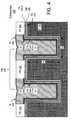
- FIG. 1illustrates another package with two intermediate substrates 110 , 120 between dies (ICs) 124 and PCB 130 .
- Intermediate substrate 110is a BT substrate, soldered to the underlying PCB 130 with solder balls 134 .
- Intermediate substrate 120is a silicon interposer attached to the top surface of BT substrate 110 by an adhesive (not shown).
- Silicon interposer 120includes metal layers 136 formed over silicon substrate 140 and separated by dielectric layers 144 . Dies 124 are attached to interposer 120 with their contact pads facing up. The dies' contact pads are wire bonded to contact pads 136 C. 1 provided by metal layers 136 . The wire bonding is done with bond wires 150 .
- Contact pads 136 C. 2 on top of the interposerare wire bonded to contact pads 360 on top of BT substrate 110 using bond wires 160 .
- Interconnect lines made from layers 136connect the contact pads 136 C. 1 to the contact pads 136 C. 2 .
- Metal layers 136provide interconnects between the dies 124 .
- the interconnectscan be manufactured on silicon interposer 120 with a higher density and higher electrical performance than on BT substrate 110 . There is no CTE mismatch between silicon substrate 120 and silicon dies 124 .
- a manufacturermay sell packaging substrates consisting substantially of a silicon interposer 120 and a BT substrate 110 ( FIG. 2 ). Then the buyers of the packaging substrates attach the dies 124 and the PCBs 130 to the packaging substrates.
- solderingWhen multiple soldering operations are performed to form different solder joints, each subsequent soldering operation should not destroy the solder joints formed in the previous operations. This can be achieved, by a solder hierarchy, i.e. a hierarchy of the solder melting temperatures. Each subsequent soldering operation is performed with a solder having a lower melting temperature then the solders used in the previous operations, so the solders used in the previous operations do not melt. It is desirable to develop techniques that relax the solder hierarchy requirements.
- a packaging substratewhich, like the packaging substrate of FIG. 2 , includes a silicon interposer and a BT substrate.
- the silicon interposerhas contact pads both on the top and the bottom, and has through-silicon vias made in the silicon substrate of the interposer. Conductive paths going through the through-silicon vias connect the contact pads on the top of the interposer to the contact pads on the bottom.
- Silicon interposers with through-silicon viashave been described in U.S. Pat. No. 6,322,903, incorporated herein by reference, but not in a packaging substrate having two or more intermediate substrates as in some embodiments of the present invention.
- the packaging substrates according to some embodiments of the present inventionprovide a manufacturing challenge if the silicon interposer is thin. Thin interposers are desirable because to reduce the package size and improve the electrical characteristics (by shortening the conductive paths through the interposer). Also, in some embodiments, it is easier to manufacture the through-silicon vias if the interposer is thin. However, thin interposers are fragile, can be warped, and their heat dissipation capabilities are poor, so the interposer handling is complicated. In U.S. Pat. No.
- the interposeris thinned only after attachment to a die.
- the interposermay have to be thinned to its final thickness before the die attachment.
- the interposeris thinned before attachment to the BT substrate.
- the semiconductor substrate of the interposercan be quite thin, e.g. 100 ⁇ m or thinner.
- the semiconductor substrate and the interposermay have substantially planar top and bottom surfaces, as opposed to interposers with cavities large enough to contain a die, with the cavities' sidewalls being thicker than the rest of the interposer to increase the interposer's mechanical strength (see U.S. patent application Ser. No. 09/952,263 filed Sep. 13, 2001 by Halahan et al., incorporated herein by reference).
- substantially planarindicates that any non-planarity of the semiconductor substrate or the interposer is so minor as to have no significant effect on the mechanical strength of the structure.
- Some aspects of the present inventionrelate to a manufacturing process, and to a BT substrate, that simplifies the handling of thin silicon interposers.
- solderingIn some embodiments of the present invention, maintaining the solder hierarchy is simplified through changing the solder melting temperature during soldering. It is well known that a solder melting temperature may increase if a soldered surface contains copper because the copper may dissolve in the solder during the soldering operation to raise the solder melting temperature. In some embodiments, this property is used to obtain a proper solder hierarchy. For example, in some embodiments, all of the sequential soldering operations use the same starting solder material. In each soldering operation, the solder's melting temperature increases, so the solder will not melt in the subsequent soldering operations. The manufacturing process is simplified because it eliminates the need to obtain different solder types with different initial melting temperatures.
- the solder for a current soldering operationmay initially have even a lower melting temperature than the solders used in the subsequent operations, but the solder melting temperature is increased in the current soldering operation to prevent the solder from melting during the subsequent operations.
- the inventionis not limited to the embodiments discussed in this section.
- the inventionis not limited to thin interposers, and further is applicable to non-silicon semiconductor interposers attached to non-BT intermediate substrates. Materials other than copper may be used to increase the solder melting temperature. Other features and advantages of the invention are described below. The invention is defined by the appended claims.
- FIGS. 1 and 2show vertical cross sections of integrated circuit packaging structures according to prior art.
- FIGS. 3–13show vertical cross sections of integrated circuit packaging structures according to some embodiments of the present invention.
- FIG. 14is a flowchart of an integrated circuit packaging process according to one embodiment of the present invention.
- FIG. 15shows a vertical cross section of an integrated circuit packaging structure according to one embodiment of the present invention.
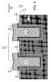
- FIG. 3illustrates an integrated circuit packaging substrate 310 having two intermediate integrated circuit packaging substrates 110 , 120 .
- Substrate 120is a silicon interposer attached to BT substrate 110 . Dies 124 and PCB 130 will be attached later.
- Silicon interposer 120includes metal layers 136 formed over silicon substrate 140 .
- Substrate 140has substantially planar top and bottom surfaces, and is quite thin. In some embodiments, the planarity of substrate 140 is suitable for fine geometry photolithography (finer than possible with BT and FR4 substrates).
- the thickness of substrate 140can be 100 ⁇ m or less (50 ⁇ m to 35 ⁇ m thickness values believed to be achievable, and smaller values may be possible).
- Layers 136provide interconnect lines and may also provide power and ground planes, resistors, inductors, capacitor plates for decoupling capacitors and other capacitor types, and possibly other elements, known or to be invented. Layers 136 can be separated from each other, and from the substrate, by dielectric layers 144 .
- Layers 136contact each other and the silicon substrate through openings in the dielectric layers. Layers 136 can also be formed directly on the silicon substrate if desired. Layers 136 provide contact pads 136 C at the top surface of the interposer. The contact pads are available for flip-chip attachment to dies 124 .
- Silicon substrate 140includes metalized through-silicon vias 330 that pass between the top and bottom surfaces of substrate 140 . Conductive paths are provided from contact pads 136 C at the top of the interposer to contact pads 340 at the bottom of the interposer through the vias 330 . Contact pads 340 are attached to contact pads 350 at the top surface of BT substrate 110 .
- Interconnects (not shown) in BT substrate 110connect the contact pads 350 to contact pads 360 at the bottom surface of substrate 110 .
- Solder balls 134are formed on pads 360 by conventional techniques for attachment to PCB 130 .
- the size and spacing (pitch) of contact pads 136 C on interposer 120matches the size and the pitch of the contact pads on dies 124 . If dies 124 are silicon integrated circuits, their CTE matches the CTE of the interposer, so the pitch of contact pads 136 C can be small because the low thermal stresses at the interface between the dies and the interposer make it unnecessary to use large solder balls 370 .
- the contact pads 340 on the bottom of the interposermatch the top contact pads 350 of BT substrate 110 . For some fabrication technologies, the minimum dimensions are as shown in the following table. The dimensions can typically be reduced if more expensive technologies are used.
- the metal contact pads 340are formed to protrude out of vias 330 .
- the protruding contact pads 340are inserted into cavities in BT substrate 110 , as explained in more detail below.
- the inventionis not limited to the protruding contact pads or the cavities however.
- Silicon interposer 120can be manufactured using conventional techniques. See e.g. the aforementioned U.S. Pat. No. 6,322,903. Other techniques are described in U.S. patent application Ser. No. 10/410,929 filed on Apr. 9, 2003 by P. Halahan et al., entitled “Electroplating and electroless plating of conductive materials into openings, and structures obtained thereby”, incorporated herein by reference. Still other techniques can possible be used, whether known or to be invented.
- DRIEdeep reactive ion etching
- the via diameter Dvis 251 ⁇ m to 100 ⁇ m.
- Silicon dioxide layer 410is thermally grown on the wafer to a thickness of about 1 ⁇ m. A larger thickness can also be used to reduce the capacitance between substrate 140 and the metal features that will be fabricated in vias 330 .
- Barrier layer 420 of titanium-tungsten (TiW)is sputtered on oxide 410 to a thickness of 0.2 ⁇ m.
- a seed copper (Cu) layer 430 . 1is sputtered on the wafer to a thickness sufficient to ensure a continuous copper coverage in the via. Thicknesses of 0.5 ⁇ m to 21 ⁇ m are believed to be adequate, depending on the sputter technology.
- a dry photoresist film 440is deposited on the wafer and patterned to expose the vias 330 .
- gold (Au) layer 444 and nickel (Ni) layer 448are electroplated, in that order, to an exemplary thickness of 0.2 ⁇ m and 1.0 ⁇ m respectively.
- Copper 430 . 2is electroplated on nickel 448 to fill the vias 330 and possibly protrude out of the vias.
- the cathode terminal (not shown) of the power sourceis placed at the periphery of wafer 140 in physical contact with seed layer 430 . 1 .
- nickel (Ni) layer 450is electroplated on the top surface of copper layer 430 . 2 to an exemplary thickness of 0.5 ⁇ m.
- Resist 440is removed ( FIG. 5 ).
- a wet copper etchremoves the exposed portions of seed copper 430 . 1 , with nickel 450 acting as a mask.
- Nickel 450protects copper 430 . 2 in vias 330 .
- Copper 430 . 2 , 430 . 1can be etched laterally during the wet etch, but the lateral etch does not remove the copper over the vias 330 because the copper extends laterally beyond the via edges.
- the copper etchmay reduced the thickness of copper 430 . 2 , but this is acceptable if the copper protrusions above the vias are sufficiently thick. In either case, it is desirable for the top surface of copper 430 . 2 to be at or above the top surface of oxide 410 after the copper etch.
- a CMP step(chemical mechanical polishing) is performed to remove copper 430 . 2 , nickel 448 , gold 444 , and TiW 420 off the top surface of substrate 140 ( FIG. 6 ).
- the CMPstops on oxide 410 .
- the structurehas a planar top surface.
- the wet etch of copper 430 . 1is omitted, and copper 430 . 1 is removed by the CMP step.
- the separate wet etch of copper 430 . 1may be desirable however because it may shorten the more expensive CMP step, thus reducing the total manufacturing cost.
- Oxide 410can be patterned if desired.
- Metal layers 136 ( FIG. 7 ) and dielectric layers 144are deposited on the interposer wafer and patterned to provide interconnects and, possibly, other elements as described above.
- metal 136is copper and dielectric 144 is polyimide, but other materials can also be used.
- Some or all of dielectric layers 144can be silicon dioxide, photosensitive benzocyclobutene (BCB), polybenzoxazole (PBO), or other materials.
- a high dielectric constant materialsuch as Ta 2 O 5
- Aluminum, conductive polysilicon, and other materialscan be used as layers 136 .
- Solder wettable materialse.g. Ni or Au
- the interposer waferis thinned from the bottom to expose the gold 444 . See FIG. 8 .
- the exposed metalprovides the contact pads 340 ( FIG. 3 ) that will be soldered to BT substrate 110 .
- the wafer thinningcan be performed with any of the techniques described in the aforementioned U.S. Pat. No. 6,322,903 and U.S. patent application Ser. No. 10/410,929. See also U.S. Pat. No. 6,498,381 issued on Dec. 24, 2002 to Halahan et al. and incorporated herein by reference.
- the wafer thinningincludes a CF 4 plasma etch at atmospheric pressure.
- the plasma etchexposes the oxide 410 and then etches the silicon 140 , oxide 410 and TiW 420 selectively to copper 430 . 1 . (Copper 430 . 1 is etched later as explained below.)
- the plasma etchetches silicon 140 faster than oxide 410 , so the oxide protrudes out of the silicon on the bottom surface of the wafer after the etch.
- the final thickness “Tsif”(marked in FIG. 8 ) of silicon substrate 140 is 100 ⁇ m, and it can be smaller (e.g. 35 ⁇ m).
- Oxide 410 and TiW 420form 5 ⁇ m protrusions around the copper 430 . 1 below the silicon surface.
- the plasma etchforms copper oxide (not shown) on the exposed portions of copper 430 . 1 .
- the copper oxide and the copper 430 . 1are etched by a wet etch to expose gold 444 .
- the goldprovides a solderable oxide-free surface.
- Nickel 448will prevent copper diffusion from layer 430 . 2 into the solder.
- the copper diffusionmay be undesirable because it increases the solder melting temperature.
- the copper diffusionis desirable to achieve a certain solder hierarchy (the hierarchy of the melting temperatures of different solders) as explained below.
- the etch of copper 430 . 1can be omitted.
- gold 444can be omitted.
- the etch of copper 430 . 1will then expose nickel 448 .
- the copper 430 . 1is not etched away.
- the copper oxide (not shown) on copper 430 . 1can be removed by a wet etch.
- the copper oxidecan also be removed by a solder flux during soldering of the interposer wafer to BT substrate 110 (the soldering operation is described below).
- Layers 444 , 448can be omitted.
- Metal contact pads 340are metal protrusions formed by the metal layers 430 . 2 , 448 , 444 , 430 . 1 , 420 below the bottom surface of silicon 140 .
- the height Hd of metal contact pads 340is 50 ⁇ m.
- a dielectric layer(not shown) can optionally be formed on the bottom surface of the interposer to cover the silicon 140 but not the metal contact pads 340 .
- the dielectriccan be formed without photolithography. See the aforementioned U.S. Pat. Nos. 6,322,903 and 6,498,381 and U.S. patent application Ser. No. 10/410,929.
- the interposer wafercan be diced if desired.
- the dicingcan be performed at the same time as the interposer wafer thinning if vias were formed along the dicing lines (scribe lines) simultaneously with vias 330 at the stage of FIG. 4 .
- U.S. Pat. No. 6,498,074 issued Dec. 24, 2002 to Siniaguine et al.entitled “THINNING AND DICING OF SEMICONDUCTOR WAFERS . . . ”, incorporated herein by reference.
- the interposer waferis not diced. ICs 124 will be attached to the wafer.
- metal 430 . 2does not fill the through-silicon vias.
- Metal 430 . 2is a thin film deposited over the via sidewalls, and it can be part of a layer 136 . See the aforementioned U.S. Pat. No. 6,498,381. Also, in some embodiments the contact pads 340 do not protrude out of the bottom surface of the interposer.
- Interposer 120(diced or undiced) can be attached to a conventional BT substrate 110 with solder, conductive epoxy, anisotropic adhesive, thermocompression, or possibly by other techniques, known or to be invented. In some embodiments, however, specially processed BT substrates are used to minimize the interposer handling.
- the interposer handlingshould preferably be minimized if the interposer is thin.
- the interposer's silicon substrate 140can be 100 ⁇ m or thinner, the interposer can be fragile, and its heat dissipation capability can be low. Also, the interposer can be warped. Further, some conventional soldering techniques, e.g.
- the techniques that involve electroplating of solder and under-ball metallurgy layers on contact pads 340may require photolithography on the bottom surface of the interposer.
- the use of photolithographyis undesirable because of possible wafer damage and mask misalignment.
- the use of a conventional BT substratecan also be difficult due to a possibly non-uniform height of protruding contact pads 340 . Those contact pads 340 that have a smaller height may be unable to reach the BT substrate contact pads 350 ( FIG. 3 ). Therefore, a specially processed BT substrate 110 is used in some embodiments, as shown in FIGS. 9 and 10 .
- BT substrate 110 of FIGS. 9 and 10is formed from one or more BT layers laminated in a conventional manner. Three layers 110 . 1 , 110 . 2 , 110 . 3 are shown, but any number of layers can be present.
- Thin film metal layers 910e.g. copper
- Layers 910are interconnected through vias in the BT layers 110 .i(i.e. 110 . 1 , 110 . 2 , 110 . 3 ) using known techniques to provide conductive paths between contact pads 350 and contact pads 360 .
- the bottom metal layer 910provides contact pads 360 ( FIG. 3 ) at the bottom surface of BT substrate 110 .
- the difference between the BT substrate 110 of FIG. 9 and a conventional BT substrateis that the top contact pads 350 , and the top metal layer 910 , are formed below the top BT layer 110 . 3 .
- the top contact pads 350 and the top metal 910are formed on BT layer 110 . 2 .
- Layer 110 . 3has vias 920 exposing the contact pads 350 . Vias 920 form cavities in the top surface of BT substrate 110 . Silicon interposer contact pads 340 will be inserted into these cavities to form a reliable mechanical and electrical contact.
- Dccan be calculated starting with the diameter Dv ( FIG. 4 ) of via 330 , by subtracting double the thickness of the layers 410 , 420 , 430 . 1 , 444 , 448 .
- the depth Hcav of each cavity 920(about equal to the thickness of layer 110 . 3 ) is 50 ⁇ m for a 50 ⁇ m height Hd of contact pads 340 (Hcav is measured to the top surface of contact pads 350 ).
- Cavities 920are filled with solder paste 930 .
- the solder pasteis deposited to cover the BT substrate, and then is wiped off by a squeegee blade to force the solder into cavities 920 and remove it from the top surface of BT layer 110 . 3 .
- the solderis chosen to have a high melting temperature to provide a desired solder hierarchy for subsequent solder attachment of dies 124 and PCB 130 .
- the solder pasteis a no-clean type NC253 available from AIM of Montreal, Canada. This paste incorporates solder flux but there is no need to clean the flux after the solder reflow.
- No-flow underfill 940(dielectric) is dispensed on BT substrate 110 at the future site of interposer 120 .
- the underfillis type STAYCHIPTM 2078E available from Cookson Electronics, a company having an office in Georgia, the United States of America. This underfill performs both the underfill function and the solder flux function.
- the underfillcan be dispensed with a dispensing system of type CAMELOT/SPEEDLINE 1818 available from Cookson Electronics.
- Interposer wafer 120is placed on BT substrate 110 ( FIG. 10 ).
- Protruding contact pads 340enter the cavities 920 and contact the solder 930 but do not necessarily reach the metal 910 of contact pads 350 .
- a uniform height of contact pads 340is not required for a good electrical contact.
- Underfill 940spreads out under the interposer. In the embodiment shown, the bottom surface of silicon 140 does not reach the BT substrate. Underfill 940 helps insulate the silicon from solder 930 . Therefore, it is unnecessary to form a dielectric layer on the bottom silicon surface.
- the interposer placementcan be performed with a placement tool of type SIPLACE F4 available from Siemens corporation of Germany.
- the placement toolpicks up the interposer from the top by a vacuum holder 1010 schematically shown in FIG. 10 .
- the vacuum pick-upflattens the interposer if the interposer is warped.
- Dielectric 144protects the interposer from being damaged by the holder.
- Other placement tools, with vacuum and non-vacuum holders, known or to be invented,can also possibly be used.
- the structureis heated to reflow the solder paste 930 and cure the underfill 940 .
- the solderwets the bottom and side surfaces of copper contact pads 340 .
- the final value of the gap G 1 between the silicon 140 and the BT substrate 110is 25 ⁇ m.
- the gap values of 5 to 10 ⁇ m and largerare believed to be appropriate to provide sufficient electrical insulation if no dielectric is formed on the bottom surface of silicon 140 .
- the value C 1is in the range from 10 ⁇ m to 45 ⁇ m in some embodiments.
- vacuum holder 1010releases the interposer.
- the vacuum holderreleases the interposer before the solder reflow.
- the interposerstays in place due to a surface tension between silicon 140 and the underfill 940 .
- Multiple interposerscan be placed on BT substrate 110 , and the solder reflow and underfill curing can be performed in a single heating step for all the interposers.
- a similar techniquehas previously been applied for flip-chip mounting of dies on a BT substrate, as described in M. Painaik and J. Hurtley, “Process Recommendations for Assembly of Flip Chips using No-flow Underfill”, Technical Bulletin, Cookson Semiconductor.
- FIG. 11illustrates another embodiment.
- the BT substrate 110is similar to the BT substrate of FIGS. 9 and 10 , but a metal layer 1110 is formed on the bottom and sidewalls of each cavity 920 .
- Metal 1110is believed to improve the strength and the electrical conductivity of the solder bond between contact pads 340 and contact pads 350 .
- Metal layer 1110can be copper deposited on the BT substrate and patterned by lift-off or some other process. In FIG. 11 , metal 1110 extends out of cavities 920 to the top surface of the BT layer 110 . 3 but does not provide any interconnects or other elements on the top surface of layer 110 . 3 .
- Metal 1110is present only in the immediate vicinity of each cavity 920 .
- Each contact 350includes the portions of metal layers 910 , 1110 on the bottom and sidewalls of the corresponding cavity 920 .
- metal 1110provides an additional level of interconnects and/or a power or ground plane on layer 110 . 3 .
- the BT layers 110 . 1 , 110 . 2 , 110 . 3are laminated on top of each other.
- Each layer 110 . 1 , 110 . 2is a solid sheet placed laminated on the structure in a solid form.
- the top layer 110 . 3is made from a material different from the material of layers 110 . 1 , 110 . 2 .
- solder dam materialscan be used, such as photoimageable polyimide, Dupont VACREL 8100, Dupont Flexible PhotoImageable Coverlay (PIC) 1000 & 2000, Shipley (Dynachem) DynaMASK 5000, Shipley ConforMASK 2500, and possibly others.
- Some of the solder dam materialse.g. polyimide
- FIG. 12is similar to FIG. 11 , but solder balls 1210 have been attached to contact pads 136 C. Solder balls 1210 eliminate the need for solder balls 370 ( FIG. 3 ) on dies 124 .
- the packaging substrate manufacturercan provide solder balls 1210 to simplify the die 124 attachment for the substrate buyers.
- Solder 1210can be attached to the interposer at any fabrication stage. In one embodiment, solder 1210 is attached to pads 136 C before the interposer wafer is thinned, i.e. before the stage of FIG. 8 . The interposer wafer is mechanically stronger at this stage and its heat dissipating capability is higher, so the interposer handling is easier.
- Metal 1110may be omitted (as in FIG. 10 ).
- solder 1210has a lower melting temperature than solder 930 . Therefore, solder 930 is not melted during the attachment of dies 124 .
- solder 1210has the same or higher melting temperature than solder 930 , but the melting temperature of solder 930 is increased during the attachment of interposer 120 to BT substrate 110 .
- the melting temperature of solder 930becomes higher than the melting temperature of solder 1210 .
- the melting temperature of solder 930is increased because the copper from layer 1110 and/or layer 350 dissolves in solder 930 .
- copper 430 . 1was not etched away as in FIG. 8 , so copper 430 . 1 can also dissolve in the solder.
- solders 1210 , 930are initially the same solder (i.e. the same material), which simplifies the wafer fabrication. For example, a eutectic solder Sn/Ag3.0/Cu0.5 (known as type LF128 from AIM) can be used.
- Metal contact pads 136 Ccan be formed from a material other than copper.
- interconnects 136are made of copper, but contact pads 136 C are plated with a layer 1220 of nickel or gold.
- Layer 1220does not dissolve in solder 1210 and provides a barrier for the copper diffusion from interconnects 136 , so the melting temperature of solder 1210 does not change.
- the melting temperature of solder 1210changes during the attachment of the interposer to substrate 110 , but the melting temperature of solder 1210 remains below the melting temperature of solder 930 .
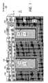
- FIGS. 13–14illustrate a possible manufacturing sequence with multiple die levels 124 . 1 , 124 . 2 , 124 . 3 attached to the packaging substrate.
- the packaging substrateis manufactured as in FIG. 12 .
- the interposer viasare marked 330 . 0 (instead of 330 as in FIG. 12 ), the contact pads at the bottom of the interposer are marked 340 . 0 , and the solder at the top is marked 1210 . 0 .
- Each die 124 . 1has one or more metalized through vias 330 . 1 formed in the die's semiconductor substrate 140 . 1 (e.g. monocrystalline silicon). Each via 330 . 1 passes between the top and bottom surfaces of substrate 140 . 1 . Conductive paths are provided from contact pads at the top of the die 124 . 1 to contact pads 340 . 1 at the bottom of the die through the vias 330 . 1 . Contact pads 340 . 1 protrude out of the respective vias 330 . 1 .
- the dies 124 . 1can be manufactured using the same techniques as described above for interposer 120 (involving the wafer thinning to expose the contact pads 340 . 1 ). Each die may have the same general structure as interposer 120 in FIG.
- circuitry in dies 124 . 1does not have to be identical to the interposer circuitry, and different dies 124 . 1 may differ from each other.
- contact pads 340 . 1may have smaller dimensions, and may be placed closer to each other, as they do not have to meet the BT substrate dimension requirements.
- Pads 340 . 1can be copper/nickel/gold structures as in FIG. 12 , or they can be made from other materials.
- the metal in vias 330 . 1is insulated from substrate 140 . 1 by a dielectric 410 ( FIG. 12 ).
- dies 124 . 1have devices (e.g. transistors, diodes, and others) manufactured at the top surface (active surface).
- Solder balls 1210 . 1are attached to the contact pads on top of the dies, possibly before the wafer thinning operation exposing the contact pads 340 . 1 , as in FIG. 12 .
- Dies 124 . 2may be similar to dies 124 . 1 , but there is no solder on dies 124 . 2 .
- Dies 124 . 2include metalized vias 330 . 2 in semiconductor substrates 140 . 2 , and contact pads 340 . 2 protruding out of the vias.
- the active surface of dies 124 . 2is the top surface in some embodiments.
- the third level dies 124 . 3are like dies 124 in FIG. 3 . Their active surface is the bottom surface. Solder 370 is attached to the bottom contact pads.
- solder 1210 . 0is attached to interposer 120 , possibly before the interposer thinning (step 1410 ). Then the interposer is attached to BT substrate 110 as described above (step 1420 ). During this step, the melting temperature of solder 930 ( FIG. 12 ) increases and becomes higher than the melting temperature of solder 1210 . 0 . Solder 1210 . 0 may or may not be melted during this step. The melting of solder 1210 . 0 does not present a problem because the dies 124 . 1 have not yet been attached to the interposer.
- all of solders 120 . 0 , 120 . 1 , 930 , 370are initially the same material.
- the soldersare eutectic type LF 128 described above, with the initial melting temperature of 218° C.
- the melting temperature of solder 930increases to about 230° C. in step 1420 .
- dies 124 . 1are soldered to interposer 120 with solder 1210 . 0 , at a temperature of about 218° C. or higher, but below 230° C. not to melt the solder 930 .
- the copper from contact pads 340 . 1dissolves in solder 1210 . 0 and increases its melting temperature to about 230° C.
- Solder 1210 . 1may melt, but its melting temperature does not increase because the solder 1210 . 1 is not in contact with copper or other material that could increase the solder melting temperature (the top surface portions of the top contact pads of die 124 . 1 are made of suitable materials to ensure that the solder melting temperature does not increase).
- dies 124 . 2are attached to dies 124 . 1 with solder 1210 . 1 .
- Solders 1210 . 0 and 930do not melt.
- the melting temperature of solder 1210 . 1is increased to about 230° C. due to the diffusion of copper from contact pads 340 . 2 .
- dies 124 . 3are flip-chip attached to dies 124 . 2 with solder 370 .
- Solders 930 , 1210 . 0 , 1210 . 2do not melt.
- the top contact pads on dies 124 . 2may have copper to increase the melting temperature of solder 370 .
- the higher melting temperaturemay be desirable to prevent the solder melting during the attachment of BT substrate 110 to PCB 130 ( FIG. 3 ).
- the solder 134 used for the PCB attachmentmay be the same material (LF 128 ) as used for the previous steps.
- any number of diescan be used at each level.
- one or more dies 124 . 2can be attached directly to interposer 120 , i.e. there may be three levels of dies over one interposer area but only two levels of dies over another interposer area. Any number of die levels can be present in different interposer areas.
- solder types and melting temperaturescan be used, and materials other than copper can be used to increase the melting temperatures.
- materials and contact pad structurescan be used in different dies.
- the semiconductor substratescan be different semiconductor materials.
- Varying the solder melting temperature to achieve a desired solder hierarchyis not limited to the interposer structures, but may be used in other semiconductor packages, known or to be invented, with or without interposers.
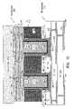
- interposer 120 and/or dies 124 . 1are provided with deep cavities 920 at the top surface to increase the mechanical strength of the solder attachment and provide a reliable electrical contact. See FIG. 15 .
- the attachment of dies 124 . 1 to interposer 120is performed by the same techniques as the attachment of the interposer to BT substrate 110 .
- the attachment of dies 124 . 2 to dies 124 . 1can also be performed in this way.
- the top dielectric layer 144 in interposer 120is a thick layer, e.g. 50 ⁇ m thick. This can be a photoimageable material such as described above for BT layer 110 . 3 . Openings in top layer 144 expose contact pads 136 C. Contact pads 340 . 1 on die 124 . 1 protrude by some distance, e.g. 50 ⁇ m, below the bottom surface of silicon substrate 140 . 1 of die 124 . 1 . The contact pads are inserted into the cavities in the top surface of the interposer. These cavities are the openings in top layer 144 that expose the contact pads 136 C.
- Metal layer 1110(e.g. gold or nickel) can be deposited on the sidewalls and bottom of the vias in top layer 144 to improve the electrical connection and provide a barrier against copper 136 diffusion into solder 1210 . 0 .
- metal 1110can be plated only on the bottom of the openings to provide a copper diffusion barrier.
- the same dimensionsare obtained as for the attachment between the BT substrate and the interposer, i.e. the final value of the gap between the silicon 140 . 1 and interposer 120 is 25 ⁇ m (gap values of 5 to 10 ⁇ m and larger are believed to be appropriate to provide sufficient electrical insulation if no dielectric is formed on the bottom surface of silicon 140 . 1 ); the contact 340 . 1 portion inside the cavities in top layer 144 is 25 ⁇ m high (note dimension C 1 in FIG. 10 ). This value is in the range from 10 ⁇ m to 45 ⁇ m in some embodiments. Other dimensions can also be used.
- Underfill(not shown) can be injected between the interposer and the dies 124 . 1 using known techniques.
- dies 124 . 1are attached to interposer 120 before the interposer is thinned. See the aforementioned U.S. Pat. No. 6,322,903.
- the attachment processcan be the same as the process of attaching the interposer to BT substrate 110 .
- solder paste 1210 . 0is placed into the cavities on top of the interposer, then a no-fill underfill is dispensed and a die or dies 124 . 1 placed on the interposer, then a heating step is performed.
- a copper diffusion barriercan be omitted. Copper 1110 and/or 136 on top of the interposer and copper 430 . 1 from dies 124 .
- solder 1210 . 0dissolves in solder 1210 . 0 to increase the solder melting temperature. Then interposer 120 is thinned and attached to BT substrate 110 . Solder 1210 . 0 will not melt during the attachment of interposer 120 to BT substrate 110 .
- the inventionis not limited to the embodiments described above.
- non-eutectic solderscan be used.
- the “melting temperature”is any temperature as high or higher than the solidus and but not higher than the liquidus.
- the solidusis the highest temperature at which 100% of solder is solid, i.e. the solder is just beginning to melt.
- the liquidusis the lowest temperature at which 100% of the solder is liquid.
- the solidus and the liquidusare the same.
- the cavities 920extend through two or more BT layers, for example, through layers 110 . 3 and 110 . 2 .
- Contact pads 350can thus be formed from the metal layer 910 located between the BT layers 110 . 1 , 110 . 2 .
- the layer 910 on BT layer 110 . 2can be used for interconnects, power or ground planes, or other elements as discussed above.
- the inventionis not limited to particular materials, dimensions and processes. For example, anisotropic adhesive, conductive epoxy, and/or thermocompression can be used instead of solder.
- the inventionis applicable to non-silicon semiconductor interposers.
- the interposermay include capacitors having a capacitance of 5.0 pF or higher.
- capacitance values of 10 pF, 100 pF, or higherhave been used on circuit boards to decouple the power lines from the ground lines or for other purposes, and such capacitors can be manufactured in the interposer.
- Resistors having resistance values of 10 ⁇ and highere.g. 50 ⁇ , 100 ⁇ , or 150 ⁇
- Inductors having inductance values of 100 nH or higherare commonly used on circuit boards and can be manufactured in the interposer.
- the inventionis not limited to particular capacitance, resistance or inductance values. Other embodiments and variations are within the scope of the invention, as defined by the appended claims.
Landscapes
- Engineering & Computer Science (AREA)
- Microelectronics & Electronic Packaging (AREA)
- Power Engineering (AREA)
- Physics & Mathematics (AREA)
- Condensed Matter Physics & Semiconductors (AREA)
- General Physics & Mathematics (AREA)
- Computer Hardware Design (AREA)
- Wire Bonding (AREA)
- Electric Connection Of Electric Components To Printed Circuits (AREA)
Abstract
Description
| Minimum | Solder ball | Solder ball | |
| Contacts | pitch | diameter | |
| Contact pads |
| 136C | 125 | μm | 60 μm (solder balls | 50 | |
| 370 on IC 124) | |||||
| 254 | |||||
| 350 | |||||
| 1.27 | mm | 0.5 mm (solder | 0.4 | mm | |
| balls 134) | |||||
Claims (23)
Priority Applications (3)
| Application Number | Priority Date | Filing Date | Title |
|---|---|---|---|
| US10/739,707US7060601B2 (en) | 2003-12-17 | 2003-12-17 | Packaging substrates for integrated circuits and soldering methods |
| PCT/US2004/042204WO2005059993A2 (en) | 2003-12-17 | 2004-12-15 | Packaging substrates for integrated circuits and soldering methods |
| US11/123,532US7034401B2 (en) | 2003-12-17 | 2005-05-05 | Packaging substrates for integrated circuits and soldering methods |
Applications Claiming Priority (1)
| Application Number | Priority Date | Filing Date | Title |
|---|---|---|---|
| US10/739,707US7060601B2 (en) | 2003-12-17 | 2003-12-17 | Packaging substrates for integrated circuits and soldering methods |
Related Child Applications (1)
| Application Number | Title | Priority Date | Filing Date |
|---|---|---|---|
| US11/123,532DivisionUS7034401B2 (en) | 2003-12-17 | 2005-05-05 | Packaging substrates for integrated circuits and soldering methods |
Publications (2)
| Publication Number | Publication Date |
|---|---|
| US20050133930A1 US20050133930A1 (en) | 2005-06-23 |
| US7060601B2true US7060601B2 (en) | 2006-06-13 |
Family
ID=34677685
Family Applications (2)
| Application Number | Title | Priority Date | Filing Date |
|---|---|---|---|
| US10/739,707Expired - LifetimeUS7060601B2 (en) | 2003-12-17 | 2003-12-17 | Packaging substrates for integrated circuits and soldering methods |
| US11/123,532Expired - LifetimeUS7034401B2 (en) | 2003-12-17 | 2005-05-05 | Packaging substrates for integrated circuits and soldering methods |
Family Applications After (1)
| Application Number | Title | Priority Date | Filing Date |
|---|---|---|---|
| US11/123,532Expired - LifetimeUS7034401B2 (en) | 2003-12-17 | 2005-05-05 | Packaging substrates for integrated circuits and soldering methods |
Country Status (2)
| Country | Link |
|---|---|
| US (2) | US7060601B2 (en) |
| WO (1) | WO2005059993A2 (en) |
Cited By (178)
| Publication number | Priority date | Publication date | Assignee | Title |
|---|---|---|---|---|
| US20080136038A1 (en)* | 2006-12-06 | 2008-06-12 | Sergey Savastiouk | Integrated circuits with conductive features in through holes passing through other conductive features and through a semiconductor substrate |
| US20080150088A1 (en)* | 2006-12-20 | 2008-06-26 | Reed Paul A | Method for incorporating existing silicon die into 3d integrated stack |
| US20090079093A1 (en)* | 2007-09-20 | 2009-03-26 | Moran John D | Flip chip structure and method of manufacture |
| US20090102021A1 (en)* | 2007-10-17 | 2009-04-23 | Chih-Hua Chen | Through-Silicon Vias and Methods for Forming the Same |
| US20090134500A1 (en)* | 2007-11-26 | 2009-05-28 | Chen-Cheng Kuo | Structures for Preventing Cross-talk Between Through-Silicon Vias and Integrated Circuits |
| US20090186430A1 (en)* | 2007-05-24 | 2009-07-23 | Chih-Hua Chen | Test Patterns for Detecting Misalignment of Through-Wafer Vias |
| US20090193584A1 (en)* | 2008-02-05 | 2009-08-06 | Standard Textile Co., Inc. | Woven contoured bed sheet with elastomeric yarns |
| US20090278238A1 (en)* | 2008-05-12 | 2009-11-12 | Texas Instruments Inc | Tsvs having chemically exposed tsv tips for integrated circuit devices |
| US20090283871A1 (en)* | 2008-05-14 | 2009-11-19 | Hung-Pin Chang | System, Structure, and Method of Manufacturing a Semiconductor Substrate Stack |
| US20090321888A1 (en)* | 2007-12-06 | 2009-12-31 | Taiwan Semiconductor Manufacturing Company, Ltd. | Alignment for backside illumination sensor |
| US20100038674A1 (en)* | 2008-08-18 | 2010-02-18 | Ding-Yuan Chen | Light-Emitting Diode With Current-Spreading Region |
| US20100062693A1 (en)* | 2008-09-05 | 2010-03-11 | Taiwan Semiconductor Manufacturing Co., Ltd. | Two step method and apparatus for polishing metal and other films in semiconductor manufacturing |
| US20100084747A1 (en)* | 2008-10-03 | 2010-04-08 | Chih-Hua Chen | Zigzag Pattern for TSV Copper Adhesion |
| US20100090304A1 (en)* | 2008-09-08 | 2010-04-15 | Taiwan Semiconductor Manufacturing Company, Ltd. | Bonding process for cmos image sensor |
| US20100117201A1 (en)* | 2008-11-13 | 2010-05-13 | Kai-Ming Ching | Cooling Channels in 3DIC Stacks |
| US20100144094A1 (en)* | 2008-12-05 | 2010-06-10 | Ming-Fa Chen | Method of Forming Stacked Dies |
| US20100140805A1 (en)* | 2008-12-10 | 2010-06-10 | Hung-Pin Chang | Bump Structure for Stacked Dies |
| US20100164109A1 (en)* | 2008-12-29 | 2010-07-01 | Wen-Chih Chiou | Backside Metal Treatment of Semiconductor Chips |
| US20100171197A1 (en)* | 2009-01-05 | 2010-07-08 | Hung-Pin Chang | Isolation Structure for Stacked Dies |
| US20100171203A1 (en)* | 2009-01-07 | 2010-07-08 | Taiwan Semiconductor Manufacturing Company | Robust TSV structure |
| US20100176494A1 (en)* | 2009-01-13 | 2010-07-15 | Ming-Fa Chen | Through-Silicon Via With Low-K Dielectric Liner |
| US20100187670A1 (en)* | 2009-01-26 | 2010-07-29 | Chuan-Yi Lin | On-Chip Heat Spreader |
| US20100193954A1 (en)* | 2009-02-04 | 2010-08-05 | Max Liu | Barrier Structures and Methods for Through Substrate Vias |
| US20100194014A1 (en)* | 2009-02-02 | 2010-08-05 | Jao Sheng Huang | Semiconductor Wafer Carrier |
| US20100220226A1 (en)* | 2009-02-24 | 2010-09-02 | Taiwan Semiconductor Manufacturing Company, Ltd. | Front side implanted guard ring structure for backside illuminated image sensor |
| US20100225002A1 (en)* | 2009-03-06 | 2010-09-09 | Taiwan Semiconductor Manufacturing Company, Ltd. | Three-Dimensional System-in-Package Architecture |
| US20100224966A1 (en)* | 2009-03-03 | 2010-09-09 | Taiwan Semiconductor Manufacturing Company, Ltd. | Stress Barrier Structures for Semiconductor Chips |
| US20100237502A1 (en)* | 2009-03-23 | 2010-09-23 | Taiwan Semiconductor Manufacturing Company, Ltd. | Barrier for Through-Silicon Via |
| US20100244247A1 (en)* | 2009-03-27 | 2010-09-30 | Taiwan Semiconductor Manufacturing Company, Ltd. | Via structure and via etching process of forming the same |
| US20100244284A1 (en)* | 2009-03-27 | 2010-09-30 | Taiwan Semiconductor Manufacturing Company, Ltd. | Method for ultra thin wafer handling and processing |
| US20100252934A1 (en)* | 2009-04-07 | 2010-10-07 | Taiwan Semiconductor Manufacturing Company, Ltd. | Three-Dimensional Semiconductor Architecture |
| US20100267217A1 (en)* | 2009-04-20 | 2010-10-21 | Taiwan Semiconductor Manufacturing Company, Ltd. | Backside Process for a Substrate |
| US20100270679A1 (en)* | 2006-10-17 | 2010-10-28 | Tessera, Inc. | Microelectronic packages fabricated at the wafer level and methods therefor |
| US20100276787A1 (en)* | 2009-04-30 | 2010-11-04 | Taiwan Semiconductor Manufacturing Company, Ltd. | Wafer Backside Structures Having Copper Pillars |
| US7829438B2 (en) | 2006-10-10 | 2010-11-09 | Tessera, Inc. | Edge connect wafer level stacking |
| US20100314758A1 (en)* | 2009-06-12 | 2010-12-16 | Taiwan Semiconductor Manufacturing Company, Ltd. | Through-silicon via structure and a process for forming the same |
| US20100330798A1 (en)* | 2009-06-26 | 2010-12-30 | Taiwan Semiconductor Manufacturing Company, Ltd. | Formation of TSV Backside Interconnects by Modifying Carrier Wafers |
| US20100330788A1 (en)* | 2009-06-30 | 2010-12-30 | Taiwan Semiconductor Manufacturing Company, Ltd. | Thin wafer handling structure and method |
| US20110006428A1 (en)* | 2009-07-08 | 2011-01-13 | Ching-Yu Lo | Liner Formation in 3DIC Structures |
| US20110027944A1 (en)* | 2009-07-30 | 2011-02-03 | Taiwan Semiconductor Maufacturing Company, Ltd. | Method of forming electrical connections |
| US20110035937A1 (en)* | 2009-08-14 | 2011-02-17 | Taiwan Semiconductor Manufacturing Company, Ltd. | Semiconductor Wafer Carrier and Method of Manufacturing |
| US20110049706A1 (en)* | 2009-09-03 | 2011-03-03 | Taiwan Semiconductor Manufacturing Company, Ltd. | Front Side Copper Post Joint Structure for Temporary Bond in TSV Application |
| US7901989B2 (en) | 2006-10-10 | 2011-03-08 | Tessera, Inc. | Reconstituted wafer level stacking |
| US20110065238A1 (en)* | 2009-09-14 | 2011-03-17 | Taiwan Semiconductor Manufacturing Company, Ltd. | Protection layer for adhesive material at wafer edge |
| US20110068466A1 (en)* | 2009-09-22 | 2011-03-24 | Taiwan Semiconductor Manufacturing Company, Ltd. | Wafer Backside Interconnect Structure Connected to TSVs |
| US20110078127A1 (en)* | 2009-09-27 | 2011-03-31 | Alibaba Group Holding Limited | Searching for information based on generic attributes of the query |
| US20110081749A1 (en)* | 2009-10-01 | 2011-04-07 | Taiwan Semiconductor Manufacturing Company, Ltd. | Surface modification for handling wafer thinning process |
| US20110084365A1 (en)* | 2009-10-09 | 2011-04-14 | Taiwan Semiconductor Manufacturing Company, Ltd. | Through Silicon Via (TSV) Wire Bond Architecture |
| US20110101527A1 (en)* | 2009-11-05 | 2011-05-05 | Taiwan Semiconductor Manufacturing Company, Ltd. | Mechanisms for forming copper pillar bumps |
| US20110108940A1 (en)* | 2009-11-06 | 2011-05-12 | Taiwan Semiconductor Manufacturing Company, Ltd. | Method of fabricating backside-illuminated image sensor |
| US20110108986A1 (en)* | 2009-11-09 | 2011-05-12 | Taiwan Semiconductor Manufacturing Company, Ltd. | Through-silicon via structure and a process for forming the same |
| US7952195B2 (en) | 2006-12-28 | 2011-05-31 | Tessera, Inc. | Stacked packages with bridging traces |
| US20110133335A1 (en)* | 2008-12-31 | 2011-06-09 | Taiwan Semiconductor Manufacturing Company, Ltd. | Through-Silicon Via With Air Gap |
| US20110169168A1 (en)* | 2009-02-24 | 2011-07-14 | Taiwan Semiconductor Manufacturing Company, Ltd. | Through-silicon via formed with a post passivation interconnect structure |
| US20110177655A1 (en)* | 2007-06-27 | 2011-07-21 | Taiwan Semiconductor Manufacturing Company, Ltd. | Formation of Through Via before Contact Processing |
| US20110193221A1 (en)* | 2010-02-05 | 2011-08-11 | Taiwan Semiconductor Manufacturing Company, Ltd. | 3DIC Architecture with Interposer for Bonding Dies |
| US20110193219A1 (en)* | 2010-02-09 | 2011-08-11 | Taiwan Seimconductor Manufacturing Company, Ltd. | Semiconductor device and semiconductor assembly with lead-free solder |
| US20110198747A1 (en)* | 2010-02-16 | 2011-08-18 | Taiwan Semicondcutor Manufactoring Company, Ltd. | Conductive pillar structure for semiconductor substrate and method of manufacture |
| US20110198638A1 (en)* | 2010-02-16 | 2011-08-18 | Taiwan Semiconductor Manufacturing Company, Ltd. | Light-emitting diode (led) package systems |
| US20110198721A1 (en)* | 2010-02-12 | 2011-08-18 | Taiwan Semiconductor Manufacturing Company, Ltd. | Method for thinning a wafer |
| US20110217841A1 (en)* | 2009-10-22 | 2011-09-08 | Taiwan Semiconductor Manufacturing Company, Ltd. | Method of forming through silicon via with dummy structure |
| US20110233762A1 (en)* | 2010-03-25 | 2011-09-29 | International Business Machines Corporation | Wafer level integrated interconnect decal and manufacturing method thereof |
| US20110233761A1 (en)* | 2009-07-30 | 2011-09-29 | Taiwan Semiconductor Manufacturing Company, Ltd. | Cu pillar bump with non-metal sidewall protection structure |
| US8043895B2 (en) | 2007-08-09 | 2011-10-25 | Tessera, Inc. | Method of fabricating stacked assembly including plurality of stacked microelectronic elements |
| US8168529B2 (en) | 2009-01-26 | 2012-05-01 | Taiwan Semiconductor Manufacturing Company, Ltd. | Forming seal ring in an integrated circuit die |
| US8174124B2 (en) | 2010-04-08 | 2012-05-08 | Taiwan Semiconductor Manufacturing Co., Ltd. | Dummy pattern in wafer backside routing |
| US20120153466A1 (en)* | 2009-09-02 | 2012-06-21 | Hwee-Seng Jimmy Chew | Package structure |
| US8222139B2 (en) | 2010-03-30 | 2012-07-17 | Taiwan Semiconductor Manufacturing Company, Ltd. | Chemical mechanical polishing (CMP) processing of through-silicon via (TSV) and contact plug simultaneously |
| US8236584B1 (en) | 2011-02-11 | 2012-08-07 | Tsmc Solid State Lighting Ltd. | Method of forming a light emitting diode emitter substrate with highly reflective metal bonding |
| US8247906B2 (en) | 2009-07-06 | 2012-08-21 | Taiwan Semiconductor Manufacturing Company, Ltd. | Supplying power to integrated circuits using a grid matrix formed of through-silicon vias |
| US8319336B2 (en) | 2010-07-08 | 2012-11-27 | Taiwan Semiconductor Manufacturing Company, Ltd. | Reduction of etch microloading for through silicon vias |
| US8324738B2 (en) | 2009-09-01 | 2012-12-04 | Taiwan Semiconductor Manufacturing Company, Ltd. | Self-aligned protection layer for copper post structure |
| US8338939B2 (en) | 2010-07-12 | 2012-12-25 | Taiwan Semiconductor Manufacturing Company, Ltd. | TSV formation processes using TSV-last approach |
| US8362591B2 (en) | 2010-06-08 | 2013-01-29 | Taiwan Semiconductor Manufacturing Co., Ltd. | Integrated circuits and methods of forming the same |
| US8411459B2 (en) | 2010-06-10 | 2013-04-02 | Taiwan Semiconductor Manufacturing Company, Ltd | Interposer-on-glass package structures |
| US8431435B2 (en) | 2006-10-10 | 2013-04-30 | Tessera, Inc. | Edge connect wafer level stacking |
| US8441124B2 (en) | 2010-04-29 | 2013-05-14 | Taiwan Semiconductor Manufacturing Company, Ltd. | Cu pillar bump with non-metal sidewall protection structure |
| US8445296B2 (en) | 2011-07-22 | 2013-05-21 | Taiwan Semiconductor Manufacturing Company, Ltd. | Apparatus and methods for end point determination in reactive ion etching |
| US8455995B2 (en) | 2010-04-16 | 2013-06-04 | Taiwan Semiconductor Manufacturing Company, Ltd. | TSVs with different sizes in interposers for bonding dies |
| US8456008B2 (en) | 2007-12-21 | 2013-06-04 | Taiwan Semiconductor Manufacturing Company, Ltd. | Structure and process for the formation of TSVs |
| US8461045B2 (en) | 2008-10-09 | 2013-06-11 | Taiwan Semiconductor Manufacturing Company, Ltd. | Bond pad connection to redistribution lines having tapered profiles |
| US8461672B2 (en) | 2007-07-27 | 2013-06-11 | Tessera, Inc. | Reconstituted wafer stack packaging with after-applied pad extensions |
| US8466542B2 (en) | 2009-03-13 | 2013-06-18 | Tessera, Inc. | Stacked microelectronic assemblies having vias extending through bond pads |
| US8466059B2 (en) | 2010-03-30 | 2013-06-18 | Taiwan Semiconductor Manufacturing Company, Ltd. | Multi-layer interconnect structure for stacked dies |
| US8471358B2 (en) | 2010-06-01 | 2013-06-25 | Taiwan Semiconductor Manufacturing Company, Ltd. | 3D inductor and transformer |
| US8476735B2 (en) | 2007-05-29 | 2013-07-02 | Taiwan Semiconductor Manufacturing Company, Ltd. | Programmable semiconductor interposer for electronic package and method of forming |
| US20130178063A1 (en)* | 2012-01-11 | 2013-07-11 | United Microelectronics Corp. | Method of manufacturing semiconductor device having silicon through via |
| US8487410B2 (en) | 2011-04-13 | 2013-07-16 | Taiwan Semiconductor Manufacturing Company, Ltd. | Through-silicon vias for semicondcutor substrate and method of manufacture |
| US8502338B2 (en) | 2010-09-09 | 2013-08-06 | Taiwan Semiconductor Manufacturing Company, Ltd. | Through-substrate via waveguides |
| US8501587B2 (en) | 2009-01-13 | 2013-08-06 | Taiwan Semiconductor Manufacturing Company, Ltd. | Stacked integrated chips and methods of fabrication thereof |
| US8500182B2 (en) | 2010-06-17 | 2013-08-06 | Taiwan Semiconductor Manufacturing Company, Ltd. | Vacuum wafer carriers for strengthening thin wafers |
| US8507358B2 (en) | 2010-08-27 | 2013-08-13 | Taiwan Semiconductor Manufacturing Company, Ltd. | Composite wafer semiconductor |
| US8507940B2 (en) | 2010-04-05 | 2013-08-13 | Taiwan Semiconductor Manufacturing Company, Ltd. | Heat dissipation by through silicon plugs |
| US8519409B2 (en) | 2010-11-15 | 2013-08-27 | Taiwan Semiconductor Manufacturing Company, Ltd. | Light emitting diode components integrated with thermoelectric devices |
| US8519538B2 (en) | 2010-04-28 | 2013-08-27 | Taiwan Semiconductor Manufacturing Company, Ltd. | Laser etch via formation |
| US8525343B2 (en) | 2010-09-28 | 2013-09-03 | Taiwan Semiconductor Manufacturing Company, Ltd. | Device with through-silicon via (TSV) and method of forming the same |
| US8525278B2 (en) | 2011-08-19 | 2013-09-03 | Taiwan Semiconductor Manufacturing Company, Ltd. | MEMS device having chip scale packaging |
| US8531035B2 (en) | 2011-07-01 | 2013-09-10 | Taiwan Semiconductor Manufacturing Company, Ltd. | Interconnect barrier structure and method |
| US8546235B2 (en) | 2011-05-05 | 2013-10-01 | Taiwan Semiconductor Manufacturing Company, Ltd. | Integrated circuits including metal-insulator-metal capacitors and methods of forming the same |
| US8546953B2 (en) | 2011-12-13 | 2013-10-01 | Taiwan Semiconductor Manufacturing Co., Ltd. | Through silicon via (TSV) isolation structures for noise reduction in 3D integrated circuit |
| US8546886B2 (en) | 2011-08-24 | 2013-10-01 | Taiwan Semiconductor Manufacturing Company, Ltd. | Controlling the device performance by forming a stressed backside dielectric layer |
| US8546254B2 (en) | 2010-08-19 | 2013-10-01 | Taiwan Semiconductor Manufacturing Company, Ltd. | Mechanisms for forming copper pillar bumps using patterned anodes |
| US8551815B2 (en) | 2007-08-03 | 2013-10-08 | Tessera, Inc. | Stack packages using reconstituted wafers |
| US8552485B2 (en) | 2011-06-15 | 2013-10-08 | Taiwan Semiconductor Manufacturing Company, Ltd. | Semiconductor structure having metal-insulator-metal capacitor structure |
| US8567837B2 (en) | 2010-11-24 | 2013-10-29 | Taiwan Semiconductor Manufacturing Company, Ltd. | Reconfigurable guide pin design for centering wafers having different sizes |
| US8580682B2 (en) | 2010-09-30 | 2013-11-12 | Taiwan Semiconductor Manufacturing Company, Ltd. | Cost-effective TSV formation |
| US8580647B2 (en) | 2011-12-19 | 2013-11-12 | Taiwan Semiconductor Manufacturing Company, Ltd. | Inductors with through VIAS |
| US8587127B2 (en) | 2011-06-15 | 2013-11-19 | Taiwan Semiconductor Manufacturing Company, Ltd. | Semiconductor structures and methods of forming the same |
| US8598695B2 (en) | 2010-07-23 | 2013-12-03 | Tessera, Inc. | Active chip on carrier or laminated chip having microelectronic element embedded therein |
| US8604491B2 (en) | 2011-07-21 | 2013-12-10 | Tsmc Solid State Lighting Ltd. | Wafer level photonic device die structure and method of making the same |
| US8604619B2 (en) | 2011-08-31 | 2013-12-10 | Taiwan Semiconductor Manufacturing Company, Ltd. | Through silicon via keep out zone formation along different crystal orientations |
| US8610247B2 (en) | 2011-12-30 | 2013-12-17 | Taiwan Semiconductor Manufacturing Company, Ltd. | Structure and method for a transformer with magnetic features |
| US8618631B2 (en) | 2012-02-14 | 2013-12-31 | Taiwan Semiconductor Manufacturing Co., Ltd. | On-chip ferrite bead inductor |
| US8629042B2 (en) | 2008-12-08 | 2014-01-14 | Taiwan Semiconductor Manufacturing Company, Ltd. | Method for stacking semiconductor dies |
| US8629563B2 (en) | 2007-07-16 | 2014-01-14 | Taiwan Semiconductor Manufacturing Company, Ltd. | Method for packaging semiconductor dies having through-silicon vias |
| US8659126B2 (en) | 2011-12-07 | 2014-02-25 | Taiwan Semiconductor Manufacturing Company, Ltd. | Integrated circuit ground shielding structure |
| US8674510B2 (en) | 2010-07-29 | 2014-03-18 | Taiwan Semiconductor Manufacturing Company, Ltd. | Three-dimensional integrated circuit structure having improved power and thermal management |
| US8674883B2 (en) | 2011-05-24 | 2014-03-18 | Taiwan Semiconductor Manufacturing Company, Ltd. | Antenna using through-silicon via |
| US8680662B2 (en) | 2008-06-16 | 2014-03-25 | Tessera, Inc. | Wafer level edge stacking |
| US8693163B2 (en) | 2010-09-01 | 2014-04-08 | Taiwan Semiconductor Manufacturing Company, Ltd. | Cylindrical embedded capacitors |
| US8703609B2 (en) | 2007-08-24 | 2014-04-22 | Taiwan Semiconductor Manufacturing Company, Ltd. | Through-substrate via for semiconductor device |
| US8716128B2 (en) | 2011-04-14 | 2014-05-06 | Tsmc Solid State Lighting Ltd. | Methods of forming through silicon via openings |
| US8716131B2 (en) | 2008-08-05 | 2014-05-06 | Taiwan Semiconductor Manufacturing Company, Ltd. | Through silicon via layout |
| US8722540B2 (en) | 2010-07-22 | 2014-05-13 | Taiwan Semiconductor Manufacturing Company, Ltd. | Controlling defects in thin wafer handling |
| US8748284B2 (en) | 2011-08-12 | 2014-06-10 | Taiwan Semiconductor Manufacturing Company, Ltd. | Method of manufacturing decoupling MIM capacitor designs for interposers |
| US8757897B2 (en) | 2012-01-10 | 2014-06-24 | Invensas Corporation | Optical interposer |
| US8766409B2 (en) | 2011-06-24 | 2014-07-01 | Taiwan Semiconductor Manufacturing Co., Ltd. | Method and structure for through-silicon via (TSV) with diffused isolation well |
| US8773866B2 (en) | 2010-12-10 | 2014-07-08 | Taiwan Semiconductor Manufacturing Company, Ltd. | Radio-frequency packaging with reduced RF loss |
| US8803322B2 (en) | 2011-10-13 | 2014-08-12 | Taiwan Semiconductor Manufacturing Company, Ltd. | Through substrate via structures and methods of forming the same |
| US8803316B2 (en) | 2011-12-06 | 2014-08-12 | Taiwan Semiconductor Manufacturing Company, Ltd. | TSV structures and methods for forming the same |
| US8809073B2 (en) | 2011-08-03 | 2014-08-19 | Taiwan Semiconductor Manufacturing Company, Ltd. | Apparatus and methods for de-embedding through substrate vias |
| US8836116B2 (en) | 2010-10-21 | 2014-09-16 | Taiwan Semiconductor Manufacturing Company, Ltd. | Wafer level packaging of micro-electro-mechanical systems (MEMS) and complementary metal-oxide-semiconductor (CMOS) substrates |
| US8846499B2 (en) | 2010-08-17 | 2014-09-30 | Taiwan Semiconductor Manufacturing Company, Ltd. | Composite carrier structure |
| US8860114B2 (en) | 2012-03-02 | 2014-10-14 | Taiwan Semiconductor Manufacturing Company, Ltd. | Structure and method for a fishbone differential capacitor |
| US8866301B2 (en) | 2010-05-18 | 2014-10-21 | Taiwan Semiconductor Manufacturing Company, Ltd. | Package systems having interposers with interconnection structures |
| US8872345B2 (en) | 2011-07-07 | 2014-10-28 | Taiwan Semiconductor Manufacturing Company, Ltd. | Forming grounded through-silicon vias in a semiconductor substrate |
| US8890293B2 (en) | 2011-12-16 | 2014-11-18 | Taiwan Semiconductor Manufacturing Company, Ltd. | Guard ring for through vias |
| US8896089B2 (en) | 2011-11-09 | 2014-11-25 | Taiwan Semiconductor Manufacturing Company, Ltd. | Interposers for semiconductor devices and methods of manufacture thereof |
| US8896136B2 (en) | 2010-06-30 | 2014-11-25 | Taiwan Semiconductor Manufacturing Company, Ltd. | Alignment mark and method of formation |
| US8900994B2 (en) | 2011-06-09 | 2014-12-02 | Taiwan Semiconductor Manufacturing Company, Ltd. | Method for producing a protective structure |
| US8913402B1 (en) | 2010-05-20 | 2014-12-16 | American Semiconductor, Inc. | Triple-damascene interposer |
| US8928127B2 (en) | 2010-09-24 | 2015-01-06 | Taiwan Semiconductor Manufacturing Company, Ltd. | Noise decoupling structure with through-substrate vias |
| US8928159B2 (en) | 2010-09-02 | 2015-01-06 | Taiwan Semiconductor Manufacturing & Company, Ltd. | Alignment marks in substrate having through-substrate via (TSV) |
| US8999179B2 (en) | 2010-07-13 | 2015-04-07 | Taiwan Semiconductor Manufacturing Company, Ltd. | Conductive vias in a substrate |
| US9018758B2 (en) | 2010-06-02 | 2015-04-28 | Taiwan Semiconductor Manufacturing Company, Ltd. | Cu pillar bump with non-metal sidewall spacer and metal top cap |
| US9024205B2 (en) | 2012-12-03 | 2015-05-05 | Invensas Corporation | Advanced device assembly structures and methods |
| US9041152B2 (en) | 2013-03-14 | 2015-05-26 | Taiwan Semiconductor Manufacturing Company, Ltd. | Inductor with magnetic material |
| US9048233B2 (en) | 2010-05-26 | 2015-06-02 | Taiwan Semiconductor Manufacturing Company, Ltd. | Package systems having interposers |
| US9059262B2 (en) | 2011-02-24 | 2015-06-16 | Taiwan Semiconductor Manufacturing Company, Ltd. | Integrated circuits including conductive structures through a substrate and methods of making the same |
| US9059026B2 (en) | 2010-06-01 | 2015-06-16 | Taiwan Semiconductor Manufacturing Company, Ltd. | 3-D inductor and transformer |
| US9087838B2 (en) | 2011-10-25 | 2015-07-21 | Taiwan Semiconductor Manufacturing Company, Ltd. | Structure and method for a high-K transformer with capacitive coupling |
| US9105628B1 (en) | 2012-03-29 | 2015-08-11 | Valery Dubin | Through substrate via (TSuV) structures and method of making the same |
| US9139420B2 (en) | 2012-04-18 | 2015-09-22 | Taiwan Semiconductor Manufacturing Company, Ltd. | MEMS device structure and methods of forming same |
| US9142586B2 (en) | 2009-02-24 | 2015-09-22 | Taiwan Semiconductor Manufacturing Company, Ltd. | Pad design for backside illuminated image sensor |
| US9153462B2 (en) | 2010-12-09 | 2015-10-06 | Taiwan Semiconductor Manufacturing Company, Ltd. | Spin chuck for thin wafer cleaning |
| US9159907B2 (en) | 2011-08-04 | 2015-10-13 | Taiwan Semiconductor Manufacturing Company, Ltd. | Hybrid film for protecting MTJ stacks of MRAM |
| US9190325B2 (en) | 2010-09-30 | 2015-11-17 | Taiwan Semiconductor Manufacturing Company, Ltd. | TSV formation |
| US9293366B2 (en) | 2010-04-28 | 2016-03-22 | Taiwan Semiconductor Manufacturing Company, Ltd. | Through-substrate vias with improved connections |
| US9293521B2 (en) | 2012-03-02 | 2016-03-22 | Taiwan Semiconductor Manufacturing Co., Ltd. | Concentric capacitor structure |
| US9299594B2 (en) | 2010-07-27 | 2016-03-29 | Taiwan Semiconductor Manufacturing Company, Ltd. | Substrate bonding system and method of modifying the same |
| US9305769B2 (en) | 2009-06-30 | 2016-04-05 | Taiwan Semiconductor Manufacturing Company, Ltd. | Thin wafer handling method |
| US9312432B2 (en) | 2012-03-13 | 2016-04-12 | Tsmc Solid State Lighting Ltd. | Growing an improved P-GaN layer of an LED through pressure ramping |
| US9323010B2 (en) | 2012-01-10 | 2016-04-26 | Invensas Corporation | Structures formed using monocrystalline silicon and/or other materials for optical and other applications |
| US9390949B2 (en) | 2011-11-29 | 2016-07-12 | Taiwan Semiconductor Manufacturing Company, Ltd. | Wafer debonding and cleaning apparatus and method of use |
| US20160233161A1 (en)* | 2012-09-20 | 2016-08-11 | Taiwan Semiconductor Manufacturing Company, Ltd. | Passive Devices in Package-on-Package Structures and Methods for Forming the Same |
| US9484211B2 (en) | 2013-01-24 | 2016-11-01 | Taiwan Semiconductor Manufacturing Company, Ltd. | Etchant and etching process |
| US9490133B2 (en) | 2013-01-24 | 2016-11-08 | Taiwan Semiconductor Manufacturing Company, Ltd. | Etching apparatus |
| US9524945B2 (en) | 2010-05-18 | 2016-12-20 | Taiwan Semiconductor Manufacturing Company, Ltd. | Cu pillar bump with L-shaped non-metal sidewall protection structure |
| US9583365B2 (en) | 2012-05-25 | 2017-02-28 | Taiwan Semiconductor Manufacturing Company, Ltd. | Method of forming interconnects for three dimensional integrated circuit |
| US9618712B2 (en) | 2012-02-23 | 2017-04-11 | Taiwan Semiconductor Manufacturing Company, Ltd. | Optical bench on substrate and method of making the same |
| US9748106B2 (en)* | 2016-01-21 | 2017-08-29 | Micron Technology, Inc. | Method for fabricating semiconductor package |
| US10180547B2 (en) | 2012-02-23 | 2019-01-15 | Taiwan Semiconductor Manufacturing Company, Ltd. | Optical bench on substrate |
| US10381254B2 (en) | 2011-11-29 | 2019-08-13 | Taiwan Semiconductor Manufacturing Co., Ltd. | Wafer debonding and cleaning apparatus and method |
| US20190259725A1 (en)* | 2017-07-21 | 2019-08-22 | United Microelectronics Corp. | Manufacturing method of die-stack structure |
| US10418311B2 (en)* | 2017-03-28 | 2019-09-17 | Micron Technology, Inc. | Method of forming vias using silicon on insulator substrate |
| US20220028699A1 (en)* | 2020-07-21 | 2022-01-27 | Infineon Technologies Austria Ag | Chip-substrate composite semiconductor device |
| US11264262B2 (en) | 2011-11-29 | 2022-03-01 | Taiwan Semiconductor Manufacturing Company, Ltd. | Wafer debonding and cleaning apparatus |
| US20230318247A1 (en)* | 2022-03-31 | 2023-10-05 | Intel Corporation | Package with multiple photonic integrated circuit dies optically coupled with each other |
Families Citing this family (105)
| Publication number | Priority date | Publication date | Assignee | Title |
|---|---|---|---|---|
| TWI245381B (en)* | 2003-08-14 | 2005-12-11 | Via Tech Inc | Electrical package and process thereof |
| US8003609B2 (en) | 2004-03-30 | 2011-08-23 | The Hospital For Sick Children | Method for ameliorating pain by modification of NMDA receptors through inhibition of Src |
| US6992374B1 (en)* | 2004-06-14 | 2006-01-31 | Cisco Technology, Inc. | Techniques for manufacturing a circuit board with an improved layout for decoupling capacitors |
| US7179738B2 (en)* | 2004-06-17 | 2007-02-20 | Texas Instruments Incorporated | Semiconductor assembly having substrate with electroplated contact pads |
| US7413995B2 (en)* | 2004-08-23 | 2008-08-19 | Intel Corporation | Etched interposer for integrated circuit devices |
| US7279407B2 (en) | 2004-09-02 | 2007-10-09 | Micron Technology, Inc. | Selective nickel plating of aluminum, copper, and tungsten structures |
| US7358444B2 (en)* | 2004-10-13 | 2008-04-15 | Intel Corporation | Folded substrate with interposer package for integrated circuit devices |
| US7411303B2 (en)* | 2004-11-09 | 2008-08-12 | Texas Instruments Incorporated | Semiconductor assembly having substrate with electroplated contact pads |
| US7495330B2 (en)* | 2005-06-30 | 2009-02-24 | Intel Corporation | Substrate connector for integrated circuit devices |
| US7863187B2 (en) | 2005-09-01 | 2011-01-04 | Micron Technology, Inc. | Microfeature workpieces and methods for forming interconnects in microfeature workpieces |
| US9299634B2 (en)* | 2006-05-16 | 2016-03-29 | Broadcom Corporation | Method and apparatus for cooling semiconductor device hot blocks and large scale integrated circuit (IC) using integrated interposer for IC packages |
| US7850060B2 (en)* | 2007-04-05 | 2010-12-14 | John Trezza | Heat cycle-able connection |
| US7748116B2 (en)* | 2007-04-05 | 2010-07-06 | John Trezza | Mobile binding in an electronic connection |
| US7645701B2 (en)* | 2007-05-21 | 2010-01-12 | International Business Machines Corporation | Silicon-on-insulator structures for through via in silicon carriers |
| US8742557B2 (en)* | 2007-06-19 | 2014-06-03 | Honeywell International Inc. | Die mounting stress isolator |
| TWI335059B (en)* | 2007-07-31 | 2010-12-21 | Siliconware Precision Industries Co Ltd | Multi-chip stack structure having silicon channel and method for fabricating the same |
| DE102007038514A1 (en)* | 2007-08-16 | 2009-02-19 | Robert Bosch Gmbh | Electrical circuit arrangement and method for producing an electrical circuit arrangement |
| KR101195786B1 (en) | 2008-05-09 | 2012-11-05 | 고쿠리츠 다이가쿠 호진 큐슈 코교 다이가쿠 | Chip-size double side connection package and method for manufacturing the same |
| US8263492B2 (en)* | 2009-04-29 | 2012-09-11 | International Business Machines Corporation | Through substrate vias |
| US8067308B2 (en)* | 2009-06-08 | 2011-11-29 | Stats Chippac, Ltd. | Semiconductor device and method of forming an interconnect structure with TSV using encapsulant for structural support |
| US8689437B2 (en)* | 2009-06-24 | 2014-04-08 | International Business Machines Corporation | Method for forming integrated circuit assembly |
| US8048794B2 (en)* | 2009-08-18 | 2011-11-01 | International Business Machines Corporation | 3D silicon-silicon die stack structure and method for fine pitch interconnection and vertical heat transport |
| US8344512B2 (en)* | 2009-08-20 | 2013-01-01 | International Business Machines Corporation | Three-dimensional silicon interposer for low voltage low power systems |
| US8391018B2 (en)* | 2009-09-28 | 2013-03-05 | Qualcomm Incorporated | Semiconductor die-based packaging interconnect |
| KR20110055973A (en)* | 2009-11-20 | 2011-05-26 | 주식회사 하이닉스반도체 | Semiconductor chip module and semiconductor package including same |
| US20110204517A1 (en)* | 2010-02-23 | 2011-08-25 | Qualcomm Incorporated | Semiconductor Device with Vias Having More Than One Material |
| US10111333B2 (en)* | 2010-03-16 | 2018-10-23 | Intersil Americas Inc. | Molded power-supply module with bridge inductor over other components |
| US9530726B2 (en)* | 2010-06-28 | 2016-12-27 | Samsung Electronics Co., Ltd. | Semiconductor device and method of fabricating the same |
| US9236341B1 (en)* | 2010-08-25 | 2016-01-12 | Xilinix, Inc. | Through-silicon vias with metal system fill |
| US9723766B2 (en) | 2010-09-10 | 2017-08-01 | Intersil Americas LLC | Power supply module with electromagnetic-interference (EMI) shielding, cooling, or both shielding and cooling, along two or more sides |
| KR20120034410A (en)* | 2010-10-01 | 2012-04-12 | 삼성전자주식회사 | Semiconductor device and fabrication method thereof |
| TWI445155B (en)* | 2011-01-06 | 2014-07-11 | Advanced Semiconductor Eng | Stacked semiconductor package and method for making the same |
| US20120193809A1 (en)* | 2011-02-01 | 2012-08-02 | Nanya Technology Corp. | Integrated circuit device and method for preparing the same |
| US8519515B2 (en) | 2011-04-13 | 2013-08-27 | United Microlectronics Corp. | TSV structure and method for forming the same |
| US8481425B2 (en) | 2011-05-16 | 2013-07-09 | United Microelectronics Corp. | Method for fabricating through-silicon via structure |
| US8822336B2 (en) | 2011-06-16 | 2014-09-02 | United Microelectronics Corp. | Through-silicon via forming method |
| US8828745B2 (en) | 2011-07-06 | 2014-09-09 | United Microelectronics Corp. | Method for manufacturing through-silicon via |
| US8691691B2 (en) | 2011-07-29 | 2014-04-08 | International Business Machines Corporation | TSV pillar as an interconnecting structure |
| US8780576B2 (en)* | 2011-09-14 | 2014-07-15 | Invensas Corporation | Low CTE interposer |
| FR2980917B1 (en)* | 2011-09-30 | 2013-09-27 | St Microelectronics Crolles 2 | METHOD FOR PRODUCING AN ELECTRICALLY CONDUCTIVE THROUGH BOND |
| US8518823B2 (en) | 2011-12-23 | 2013-08-27 | United Microelectronics Corp. | Through silicon via and method of forming the same |
| US8609529B2 (en) | 2012-02-01 | 2013-12-17 | United Microelectronics Corp. | Fabrication method and structure of through silicon via |
| CN103247569B (en)* | 2012-02-14 | 2018-04-10 | 联华电子股份有限公司 | Method for manufacturing through silicon via and structure |
| US20130233598A1 (en)* | 2012-03-08 | 2013-09-12 | International Business Machines Corporation | Flexible film carrier to increase interconnect density of modules and methods thereof |
| US10074600B2 (en) | 2012-03-30 | 2018-09-11 | Ati Technologies Ulc | Method of manufacturing interposer-based damping resistor |
| US8691600B2 (en) | 2012-05-02 | 2014-04-08 | United Microelectronics Corp. | Method for testing through-silicon-via (TSV) structures |
| US20130320565A1 (en)* | 2012-05-31 | 2013-12-05 | Broadcom Corporation | Interposer Die for Semiconductor Packaging |
| US8691688B2 (en) | 2012-06-18 | 2014-04-08 | United Microelectronics Corp. | Method of manufacturing semiconductor structure |
| US9275933B2 (en) | 2012-06-19 | 2016-03-01 | United Microelectronics Corp. | Semiconductor device |
| US8900996B2 (en) | 2012-06-21 | 2014-12-02 | United Microelectronics Corp. | Through silicon via structure and method of fabricating the same |
| US8525296B1 (en) | 2012-06-26 | 2013-09-03 | United Microelectronics Corp. | Capacitor structure and method of forming the same |
| US9508563B2 (en)* | 2012-07-12 | 2016-11-29 | Xilinx, Inc. | Methods for flip chip stacking |
| US8618648B1 (en) | 2012-07-12 | 2013-12-31 | Xilinx, Inc. | Methods for flip chip stacking |
| US20140048951A1 (en)* | 2012-08-14 | 2014-02-20 | Bridge Semiconductor Corporation | Semiconductor assembly with dual connecting channels between interposer and coreless substrate |
| US10052705B2 (en) | 2012-08-30 | 2018-08-21 | Universal Instruments Corporation | 3D TSV assembly method for mass reflow |
| US8912844B2 (en) | 2012-10-09 | 2014-12-16 | United Microelectronics Corp. | Semiconductor structure and method for reducing noise therein |
| US9236442B2 (en)* | 2012-11-26 | 2016-01-12 | Broadcom Corporation | Integration of chips and silicon-based trench capacitors using low parasitic silicon-level connections |
| US9035457B2 (en) | 2012-11-29 | 2015-05-19 | United Microelectronics Corp. | Substrate with integrated passive devices and method of manufacturing the same |
| US8866308B2 (en) | 2012-12-20 | 2014-10-21 | Intel Corporation | High density interconnect device and method |
| US8716104B1 (en) | 2012-12-20 | 2014-05-06 | United Microelectronics Corp. | Method of fabricating isolation structure |
| US9312219B2 (en)* | 2012-12-28 | 2016-04-12 | Dyi-chung Hu | Interposer and packaging substrate having the interposer |
| US9204542B1 (en)* | 2013-01-07 | 2015-12-01 | Xilinx, Inc. | Multi-use package substrate |
| US9123789B2 (en)* | 2013-01-23 | 2015-09-01 | United Microelectronics Corp. | Chip with through silicon via electrode and method of forming the same |
| US8884427B2 (en) | 2013-03-14 | 2014-11-11 | Invensas Corporation | Low CTE interposer without TSV structure |
| JP5826782B2 (en)* | 2013-03-19 | 2015-12-02 | 株式会社東芝 | Manufacturing method of semiconductor device |
| US8884398B2 (en) | 2013-04-01 | 2014-11-11 | United Microelectronics Corp. | Anti-fuse structure and programming method thereof |
| US9287173B2 (en) | 2013-05-23 | 2016-03-15 | United Microelectronics Corp. | Through silicon via and process thereof |
| US9123730B2 (en) | 2013-07-11 | 2015-09-01 | United Microelectronics Corp. | Semiconductor device having through silicon trench shielding structure surrounding RF circuit |
| US9024416B2 (en) | 2013-08-12 | 2015-05-05 | United Microelectronics Corp. | Semiconductor structure |
| US8916471B1 (en) | 2013-08-26 | 2014-12-23 | United Microelectronics Corp. | Method for forming semiconductor structure having through silicon via for signal and shielding structure |
| US9048223B2 (en) | 2013-09-03 | 2015-06-02 | United Microelectronics Corp. | Package structure having silicon through vias connected to ground potential |
| US9117804B2 (en) | 2013-09-13 | 2015-08-25 | United Microelectronics Corporation | Interposer structure and manufacturing method thereof |
| WO2015099668A1 (en)* | 2013-12-23 | 2015-07-02 | Intel Corporation | Through-body-via isolated coaxial capacitor and techniques for forming same |
| US9343359B2 (en) | 2013-12-25 | 2016-05-17 | United Microelectronics Corp. | Integrated structure and method for fabricating the same |
| US9395491B2 (en)* | 2014-02-05 | 2016-07-19 | Aurrion, Inc. | Shielding regions for photonic integrated circuits |
| US10340203B2 (en) | 2014-02-07 | 2019-07-02 | United Microelectronics Corp. | Semiconductor structure with through silicon via and method for fabricating and testing the same |
| US9472518B2 (en)* | 2014-04-04 | 2016-10-18 | Micron Technology, Inc. | Semiconductor structures including carrier wafers and methods of using such semiconductor structures |
| US9548273B2 (en) | 2014-12-04 | 2017-01-17 | Invensas Corporation | Integrated circuit assemblies with rigid layers used for protection against mechanical thinning and for other purposes, and methods of fabricating such assemblies |
| US9443799B2 (en) | 2014-12-16 | 2016-09-13 | International Business Machines Corporation | Interposer with lattice construction and embedded conductive metal structures |
| CN105070682B (en)* | 2015-07-17 | 2018-05-29 | 上海交通大学 | A kind of method for efficiently preparing silicon pinboard |
| WO2017111786A1 (en)* | 2015-12-23 | 2017-06-29 | Intel Corporation | No-flow adhesive for second and third level interconnects |
| US10276402B2 (en)* | 2016-03-21 | 2019-04-30 | Taiwan Semiconductor Manufacturing Co., Ltd. | Semiconductor package and manufacturing process thereof |
| US10204893B2 (en) | 2016-05-19 | 2019-02-12 | Invensas Bonding Technologies, Inc. | Stacked dies and methods for forming bonded structures |
| US20180005887A1 (en)* | 2016-06-30 | 2018-01-04 | International Business Machines Corporation | Through-silicon via with injection molded fill |
| US10181447B2 (en) | 2017-04-21 | 2019-01-15 | Invensas Corporation | 3D-interconnect |
| US10750614B2 (en)* | 2017-06-12 | 2020-08-18 | Invensas Corporation | Deformable electrical contacts with conformable target pads |
| US10217720B2 (en) | 2017-06-15 | 2019-02-26 | Invensas Corporation | Multi-chip modules formed using wafer-level processing of a reconstitute wafer |
| US10541209B2 (en) | 2017-08-03 | 2020-01-21 | General Electric Company | Electronics package including integrated electromagnetic interference shield and method of manufacturing thereof |
| US10541153B2 (en)* | 2017-08-03 | 2020-01-21 | General Electric Company | Electronics package with integrated interconnect structure and method of manufacturing thereof |
| US10804115B2 (en) | 2017-08-03 | 2020-10-13 | General Electric Company | Electronics package with integrated interconnect structure and method of manufacturing thereof |
| WO2019089879A1 (en) | 2017-11-02 | 2019-05-09 | Universal Instruments Corporation | Fixture to hold part before and after reflow, and method |
| US11101140B2 (en) | 2017-11-10 | 2021-08-24 | Taiwan Semiconductor Manufacturing Company, Ltd. | Semiconductor device and method of manufacture |
| US10147721B1 (en) | 2017-12-20 | 2018-12-04 | Advanced Micro Devices, Inc. | Method and apparatus for dynamic calibration of on-die-precision-resistors |
| US11276676B2 (en) | 2018-05-15 | 2022-03-15 | Invensas Bonding Technologies, Inc. | Stacked devices and methods of fabrication |
| US11158606B2 (en) | 2018-07-06 | 2021-10-26 | Invensas Bonding Technologies, Inc. | Molded direct bonded and interconnected stack |
| US11462419B2 (en) | 2018-07-06 | 2022-10-04 | Invensas Bonding Technologies, Inc. | Microelectronic assemblies |
| CN111799242A (en)* | 2019-04-09 | 2020-10-20 | 矽品精密工业股份有限公司 | Package stack structure, method for fabricating the same and carrier assembly |
| CN111799182A (en)* | 2019-04-09 | 2020-10-20 | 矽品精密工业股份有限公司 | Package stack structure and its manufacturing method |
| US11296053B2 (en) | 2019-06-26 | 2022-04-05 | Invensas Bonding Technologies, Inc. | Direct bonded stack structures for increased reliability and improved yield in microelectronics |
| US11631647B2 (en) | 2020-06-30 | 2023-04-18 | Adeia Semiconductor Bonding Technologies Inc. | Integrated device packages with integrated device die and dummy element |
| US11764177B2 (en) | 2020-09-04 | 2023-09-19 | Adeia Semiconductor Bonding Technologies Inc. | Bonded structure with interconnect structure |
| US11728273B2 (en) | 2020-09-04 | 2023-08-15 | Adeia Semiconductor Bonding Technologies Inc. | Bonded structure with interconnect structure |
| CN118302858A (en)* | 2021-09-01 | 2024-07-05 | 美商艾德亚半导体科技有限责任公司 | Stacked structure with interposer |
| US12040284B2 (en) | 2021-11-12 | 2024-07-16 | Invensas Llc | 3D-interconnect with electromagnetic interference (“EMI”) shield and/or antenna |
| WO2025072250A1 (en)* | 2023-09-25 | 2025-04-03 | WU, Chunte Richard | Integrated circuit packages and packaging substrates and methods for manufacturing integrated circuit packages |
Citations (21)
| Publication number | Priority date | Publication date | Assignee | Title |
|---|---|---|---|---|
| EP0193128A2 (en) | 1985-02-25 | 1986-09-03 | Siemens Aktiengesellschaft | Film-mounted circuit and method for its production |
| US5391514A (en)* | 1994-04-19 | 1995-02-21 | International Business Machines Corporation | Low temperature ternary C4 flip chip bonding method |
| JPH08236579A (en) | 1995-02-28 | 1996-09-13 | Sumitomo Metal Ind Ltd | Method of connecting Si chip and package |
| DE19531158A1 (en) | 1995-08-24 | 1997-02-27 | Daimler Benz Ag | Diffusion soldering method esp. for semiconductor components |
| US6163456A (en) | 1998-01-30 | 2000-12-19 | Taiyo Yuden, Co., Ltd. | Hybrid module and methods for manufacturing and mounting thereof |
| US6175158B1 (en) | 1998-09-08 | 2001-01-16 | Lucent Technologies Inc. | Interposer for recessed flip-chip package |
| WO2001045476A1 (en) | 1999-12-16 | 2001-06-21 | Strand Interconnect Ab | A module including one or more chips |
| US20010019178A1 (en) | 1999-05-18 | 2001-09-06 | International Business Machines Corporation | Method of interconnecting electronic components using a plurality of conductive studs |
| US6322903B1 (en) | 1999-12-06 | 2001-11-27 | Tru-Si Technologies, Inc. | Package of integrated circuits and vertical integration |
| US20020036340A1 (en) | 2000-09-27 | 2002-03-28 | Kabushiki Kaisha Toshiba | Stacked circuit device and method for evaluating an integrated circuit substrate using the stacked circuit device |
| US20020048916A1 (en) | 1999-03-29 | 2002-04-25 | Toshiharu Yanagida | Thinned, stackable semiconductor device having low profile |
| US20020074637A1 (en) | 2000-12-19 | 2002-06-20 | Intel Corporation | Stacked flip chip assemblies |
| US20020175421A1 (en) | 2001-05-25 | 2002-11-28 | Naoto Kimura | Semiconductor device |
| US6498074B2 (en) | 1996-10-29 | 2002-12-24 | Tru-Si Technologies, Inc. | Thinning and dicing of semiconductor wafers using dry etch, and obtaining semiconductor chips with rounded bottom edges and corners |
| US6498381B2 (en) | 2001-02-22 | 2002-12-24 | Tru-Si Technologies, Inc. | Semiconductor structures having multiple conductive layers in an opening, and methods for fabricating same |
| US20030047798A1 (en) | 2001-09-13 | 2003-03-13 | Halahan Patrick B. | Semiconductor structures with cavities, and methods of fabrication |
| US20030080437A1 (en) | 2001-10-26 | 2003-05-01 | Intel Corporation | Electronic assembly with filled no-flow underfill and methods of manufacture |
| US20030116859A1 (en) | 1997-03-10 | 2003-06-26 | Seiko Epson Corporation | Electronic component and semiconductor device, method of fabricating the same, circuit board mounted with the same, and electronic appliance comprising the circuit board |
| US20030199123A1 (en) | 2002-04-18 | 2003-10-23 | Oleg Siniaguine | Clock distribution networks and conductive lines in semiconductor integrated |
| US6661088B1 (en) | 1999-09-27 | 2003-12-09 | Kabushiki Kaisha Toshiba | Semiconductor integrated circuit device having interposer and method of manufacturing the same |
| US6903443B2 (en)* | 1997-12-18 | 2005-06-07 | Micron Technology, Inc. | Semiconductor component and interconnect having conductive members and contacts on opposing sides |
- 2003
- 2003-12-17USUS10/739,707patent/US7060601B2/ennot_activeExpired - Lifetime
- 2004
- 2004-12-15WOPCT/US2004/042204patent/WO2005059993A2/enactiveApplication Filing
- 2005
- 2005-05-05USUS11/123,532patent/US7034401B2/ennot_activeExpired - Lifetime
Patent Citations (21)
| Publication number | Priority date | Publication date | Assignee | Title |
|---|---|---|---|---|
| EP0193128A2 (en) | 1985-02-25 | 1986-09-03 | Siemens Aktiengesellschaft | Film-mounted circuit and method for its production |
| US5391514A (en)* | 1994-04-19 | 1995-02-21 | International Business Machines Corporation | Low temperature ternary C4 flip chip bonding method |
| JPH08236579A (en) | 1995-02-28 | 1996-09-13 | Sumitomo Metal Ind Ltd | Method of connecting Si chip and package |
| DE19531158A1 (en) | 1995-08-24 | 1997-02-27 | Daimler Benz Ag | Diffusion soldering method esp. for semiconductor components |
| US6498074B2 (en) | 1996-10-29 | 2002-12-24 | Tru-Si Technologies, Inc. | Thinning and dicing of semiconductor wafers using dry etch, and obtaining semiconductor chips with rounded bottom edges and corners |
| US20030116859A1 (en) | 1997-03-10 | 2003-06-26 | Seiko Epson Corporation | Electronic component and semiconductor device, method of fabricating the same, circuit board mounted with the same, and electronic appliance comprising the circuit board |
| US6903443B2 (en)* | 1997-12-18 | 2005-06-07 | Micron Technology, Inc. | Semiconductor component and interconnect having conductive members and contacts on opposing sides |
| US6163456A (en) | 1998-01-30 | 2000-12-19 | Taiyo Yuden, Co., Ltd. | Hybrid module and methods for manufacturing and mounting thereof |
| US6175158B1 (en) | 1998-09-08 | 2001-01-16 | Lucent Technologies Inc. | Interposer for recessed flip-chip package |
| US20020048916A1 (en) | 1999-03-29 | 2002-04-25 | Toshiharu Yanagida | Thinned, stackable semiconductor device having low profile |
| US20010019178A1 (en) | 1999-05-18 | 2001-09-06 | International Business Machines Corporation | Method of interconnecting electronic components using a plurality of conductive studs |
| US6661088B1 (en) | 1999-09-27 | 2003-12-09 | Kabushiki Kaisha Toshiba | Semiconductor integrated circuit device having interposer and method of manufacturing the same |
| US6322903B1 (en) | 1999-12-06 | 2001-11-27 | Tru-Si Technologies, Inc. | Package of integrated circuits and vertical integration |
| WO2001045476A1 (en) | 1999-12-16 | 2001-06-21 | Strand Interconnect Ab | A module including one or more chips |
| US20020036340A1 (en) | 2000-09-27 | 2002-03-28 | Kabushiki Kaisha Toshiba | Stacked circuit device and method for evaluating an integrated circuit substrate using the stacked circuit device |
| US20020074637A1 (en) | 2000-12-19 | 2002-06-20 | Intel Corporation | Stacked flip chip assemblies |
| US6498381B2 (en) | 2001-02-22 | 2002-12-24 | Tru-Si Technologies, Inc. | Semiconductor structures having multiple conductive layers in an opening, and methods for fabricating same |
| US20020175421A1 (en) | 2001-05-25 | 2002-11-28 | Naoto Kimura | Semiconductor device |
| US20030047798A1 (en) | 2001-09-13 | 2003-03-13 | Halahan Patrick B. | Semiconductor structures with cavities, and methods of fabrication |
| US20030080437A1 (en) | 2001-10-26 | 2003-05-01 | Intel Corporation | Electronic assembly with filled no-flow underfill and methods of manufacture |
| US20030199123A1 (en) | 2002-04-18 | 2003-10-23 | Oleg Siniaguine | Clock distribution networks and conductive lines in semiconductor integrated |
Non-Patent Citations (31)
| Title |
|---|
| "200mm Wafer Fab" Strand Interconnect, Partner for High Performance Electronics. |
| "Chapter 7: Wedge and Double Cantilever Beam Tests on a High Temperature Melt Processable Polymide Adhesive, TPER-BPDA-PA," pp. 221-242. |
| "Design Notes: understanding Ball Grid Array Packages" Electronics by Design, www.electronicsbydesign.com.au, issue 1997.10, pp. 1-4. |
| "Flip Chip Bonding in Practice" Issue No. 7, Sep. 2001, The Micro Circuit Engineering Newsletter. |
| "HPMX-5001: Demonstration Circuit Board: Application Brief 102" Hewlett Packard, pp. 1-10. |
| "Introduction to Printed Wiring Boards" Netpack Education Pool, p. 1-18. |
| "Production Qualification Report: Select Qual B: Strand Substrate on MCM MQFP Qual" Amkor Technology, Date Released: Jun. 14, 2002. |
| "Solving Soldering Hierarchy Problems by Metallurgy and Design" IBM Technical Disclosure Bulletin, IBM Corp. New York, US, vol. 33, No. 8, Jan. 1991, pp. 298-299, XP000106967,ISSN: 0018-8689. |
| "Staychip; 2078E No-Flow Fluxing Underfill; For Solding Sn/Pb eutectic solder bumps to common pad metallizations Preliminary Technical Bulletin" Semiconductor Products, Technical Bulletin; Cookson Electronics. |
| "Strand is Closing the Enterprise" Strand Interconnect AB, Viggengatan5, SE-602 09 Norrkoping Sweden, www.strandinter.se. |
| "Technical Data Sheet: No-Clean Pin-Probe Testable Solder Paste: NC253" www.aimsolder.com. |
| Ekstrom; Bjorn "Thin Film Silicon Substrates For Lead Frame Packages" Advancing Microelectronics-May/Jun. 2003, pp. 6-7. |
| Gektin, Vadim; Bar-Cohen, Avram; Witzman, Sorin "Coffin-Mason Based Fatigue Analysis of Underfilled DCAs," 1998 IEEE Transactions on Components, Packaging, and Manufacturing Technology, Part A, vol. 21, No. 4, Dec. 1998, pp. 577-584. |
| Gilleo, Ken "Substrates for Flip Chips" "Flip Chips Technology" in Area Array Packaging Handbook-Manufacturing and Assembly; K Gillio, Editor, The McGraw-Hill Companies, Inc., New York, NY. |
| Guenin, Bruce M. "The Many Flavors of Ball Grid Array Packages" Electronics Cooling, Feb. 2002, pp. 1-7. |
| Jasper, Jorg "Gold or Solder Chip Bumping, the choice is application dependent" Chip Interconnection, EM Marin, pp. 1-4. |
| Jordan, Jerry "Gold Stud Bump In Flip-Chip Applications," 2002 Palomar Technologies, Inc. |
| Lu, H. and Bailey, C. "Predicting Optimal Process Conditions for Flip-Chip Assembly Using Copper Column Bumped Dies" School of Computing and Mathematical Sciences, 2002 IEEE, 2002 Electronics Packaging Technology Conference, pp. 338-343. |
| Maiwald, Werner "Soldering SMD's Without Solder Paste" http://www.midwestpcb.com/sales/Kehoe/maiwald.htm. |
| Moon, K.W.; Boettinger, W.J.; Kattner, U.R.; Biancaniello, F.S.; Handwerker, C.A. "The Ternary Eutectic of Sn-Ag-Cu Colder Alloys" Metallury Division, Materials Science and Engineering Laboratory NIST Gaithersburg, MD 20899 USA. |
| Painaik, Mandar; and Hurley, Jim "Process Recommendations for Assembly of Flip Chips Using No-Flow Underfill" Semiconductor Products, Technical Bulletin, www.cooksonsemi.com. |
| Pang, John H.L.; Chong, D.Y.R.; Low T.H. "Thermal Cycling Analysis of Flip-Chip Solder Joint Reliability" IEEE Transactions on Components and Packaging Technologies, vol. 24, No. 4, Dec. 2001, pp. 705-712. |
| Perfecto, Eric; Lee, Kang-Wook; Hamel, Harvey; Wassick, Thomas; Cline, Christopher; Oonk, Matthew; Feger, Claudius; McHerron, Dale, "Evaluation of Cu Capping Alternatives for Polymide-Cu MCM-D" IEEE, 2001 Electronic Components and Technology Conference. |
| Sperling, Ed; Electronic News, Sep. 17, 2003. |
| Tran, S.K.; Questad, D.L.; Sammakia, B.G. "Adhesion Issues in Flip-Chip on Organic Modules," 1998 InterSociety Conference on Thermal Phenomena, pp. 263-268. |
| U.S. Appl. No. 10/739,788, entitled "Integrated Circuits and Packaging Substrates With Cavities, and Attachment Methods Including Insertion of Protruding Contact Pads into Cavities," Filed on Dec. 17, 2003. |
| U.S. Appl. No.: 10/798,540, entitled "Attachment of Integrated Circuit Structures and Other Substrates to Substrates with Vias," Filed on Mar. 10, 2004. |
| Wang, C.H.; Holmes, A.S.; Gao, S. "Laser-Assisted Bump Transfer for Flip Chip Assembly," 2000 IEEE Int'l Symp on Electronic Materials & Packaging, pp. 86-90. |
| Wang, Tie; Tung, Francisca; Foo, Louis; and Dutta, Vivek "Studies on A Novel Flip-Chip Interconnect Structure-Pillar Bump" Advanpack Solutions Pte Ltd, 2001 IEEE, 2001 Electronic Components and Technology Conference. |
| www.flipchips.com/tutorial27.html "Flipchips: Tutorial 27, Shaping Gold Stud Bumps" pp. 1-8. |
| Zama, Satoru; Baldwin, Daniel F; Hikami, Toshiya; Murata, Hideaki "Flip Chip Interconnect Systems Using Wire Stud Bumps and Lead Free Solder," 2000 IEEE Electronic Components and Technology Conference, pp. 1111-1117. |
Cited By (394)
| Publication number | Priority date | Publication date | Assignee | Title |
|---|---|---|---|---|
| US9048234B2 (en) | 2006-10-10 | 2015-06-02 | Tessera, Inc. | Off-chip vias in stacked chips |
| US8999810B2 (en) | 2006-10-10 | 2015-04-07 | Tessera, Inc. | Method of making a stacked microelectronic package |
| US9899353B2 (en) | 2006-10-10 | 2018-02-20 | Tessera, Inc. | Off-chip vias in stacked chips |
| US7901989B2 (en) | 2006-10-10 | 2011-03-08 | Tessera, Inc. | Reconstituted wafer level stacking |
| US9378967B2 (en) | 2006-10-10 | 2016-06-28 | Tessera, Inc. | Method of making a stacked microelectronic package |
| US8022527B2 (en) | 2006-10-10 | 2011-09-20 | Tessera, Inc. | Edge connect wafer level stacking |
| US8513789B2 (en) | 2006-10-10 | 2013-08-20 | Tessera, Inc. | Edge connect wafer level stacking with leads extending along edges |
| US8076788B2 (en) | 2006-10-10 | 2011-12-13 | Tessera, Inc. | Off-chip vias in stacked chips |
| US7829438B2 (en) | 2006-10-10 | 2010-11-09 | Tessera, Inc. | Edge connect wafer level stacking |
| US8461673B2 (en) | 2006-10-10 | 2013-06-11 | Tessera, Inc. | Edge connect wafer level stacking |
| US8476774B2 (en) | 2006-10-10 | 2013-07-02 | Tessera, Inc. | Off-chip VIAS in stacked chips |
| US8431435B2 (en) | 2006-10-10 | 2013-04-30 | Tessera, Inc. | Edge connect wafer level stacking |
| US8426957B2 (en) | 2006-10-10 | 2013-04-23 | Tessera, Inc. | Edge connect wafer level stacking |
| US8241959B2 (en) | 2006-10-17 | 2012-08-14 | Tessera, Inc. | Microelectronic packages fabricated at the wafer level and methods therefor |
| US20100270679A1 (en)* | 2006-10-17 | 2010-10-28 | Tessera, Inc. | Microelectronic packages fabricated at the wafer level and methods therefor |
| US20080136038A1 (en)* | 2006-12-06 | 2008-06-12 | Sergey Savastiouk | Integrated circuits with conductive features in through holes passing through other conductive features and through a semiconductor substrate |
| US20080164574A1 (en)* | 2006-12-06 | 2008-07-10 | Sergey Savastiouk | Integrated circuits with conductive features in through holes passing through other conductive features and through a semiconductor substrate |
| US8110899B2 (en)* | 2006-12-20 | 2012-02-07 | Intel Corporation | Method for incorporating existing silicon die into 3D integrated stack |
| US20080150088A1 (en)* | 2006-12-20 | 2008-06-26 | Reed Paul A | Method for incorporating existing silicon die into 3d integrated stack |
| US7952195B2 (en) | 2006-12-28 | 2011-05-31 | Tessera, Inc. | Stacked packages with bridging traces |
| US8349654B2 (en) | 2006-12-28 | 2013-01-08 | Tessera, Inc. | Method of fabricating stacked packages with bridging traces |
| US20090186430A1 (en)* | 2007-05-24 | 2009-07-23 | Chih-Hua Chen | Test Patterns for Detecting Misalignment of Through-Wafer Vias |
| US8431421B2 (en) | 2007-05-24 | 2013-04-30 | Taiwan Semiconductor Manufacturing Company, Ltd. | Test patterns for detecting misalignment of through-wafer vias |
| US8476735B2 (en) | 2007-05-29 | 2013-07-02 | Taiwan Semiconductor Manufacturing Company, Ltd. | Programmable semiconductor interposer for electronic package and method of forming |
| US8945998B2 (en) | 2007-05-29 | 2015-02-03 | Taiwan Semiconductor Manufacturing Company, Ltd. | Programmable semiconductor interposer for electronic package and method of forming |
| US9209157B2 (en) | 2007-06-27 | 2015-12-08 | Taiwan Semiconductor Manufacturing Company, Ltd. | Formation of through via before contact processing |
| US20110177655A1 (en)* | 2007-06-27 | 2011-07-21 | Taiwan Semiconductor Manufacturing Company, Ltd. | Formation of Through Via before Contact Processing |
| US9793192B2 (en) | 2007-06-27 | 2017-10-17 | Taiwan Semiconductor Manufacturing Company, Ltd. | Formation of through via before contact processing |
| US8629563B2 (en) | 2007-07-16 | 2014-01-14 | Taiwan Semiconductor Manufacturing Company, Ltd. | Method for packaging semiconductor dies having through-silicon vias |
| US8461672B2 (en) | 2007-07-27 | 2013-06-11 | Tessera, Inc. | Reconstituted wafer stack packaging with after-applied pad extensions |
| US8883562B2 (en) | 2007-07-27 | 2014-11-11 | Tessera, Inc. | Reconstituted wafer stack packaging with after-applied pad extensions |
| US8551815B2 (en) | 2007-08-03 | 2013-10-08 | Tessera, Inc. | Stack packages using reconstituted wafers |
| US8043895B2 (en) | 2007-08-09 | 2011-10-25 | Tessera, Inc. | Method of fabricating stacked assembly including plurality of stacked microelectronic elements |
| US8513794B2 (en) | 2007-08-09 | 2013-08-20 | Tessera, Inc. | Stacked assembly including plurality of stacked microelectronic elements |
| US8703609B2 (en) | 2007-08-24 | 2014-04-22 | Taiwan Semiconductor Manufacturing Company, Ltd. | Through-substrate via for semiconductor device |
| US8501612B2 (en)* | 2007-09-20 | 2013-08-06 | Semiconductor Components Industries, Llc | Flip chip structure and method of manufacture |
| US20090079093A1 (en)* | 2007-09-20 | 2009-03-26 | Moran John D | Flip chip structure and method of manufacture |
| US8476769B2 (en) | 2007-10-17 | 2013-07-02 | Taiwan Semiconductor Manufacturing Company, Ltd. | Through-silicon vias and methods for forming the same |
| US20090102021A1 (en)* | 2007-10-17 | 2009-04-23 | Chih-Hua Chen | Through-Silicon Vias and Methods for Forming the Same |
| US8227902B2 (en) | 2007-11-26 | 2012-07-24 | Taiwan Semiconductor Manufacturing Company, Ltd. | Structures for preventing cross-talk between through-silicon vias and integrated circuits |
| US8604594B2 (en) | 2007-11-26 | 2013-12-10 | Taiwan Semiconductor Manufacturing Company, Ltd. | Structures for preventing cross-talk between through-silicon vias and integrated circuits |
| US20090134500A1 (en)* | 2007-11-26 | 2009-05-28 | Chen-Cheng Kuo | Structures for Preventing Cross-talk Between Through-Silicon Vias and Integrated Circuits |
| US8900966B2 (en) | 2007-12-06 | 2014-12-02 | Taiwan Semiconductor Manufacturing Company, Ltd. | Alignment for backside illumination sensor |
| US20090321888A1 (en)* | 2007-12-06 | 2009-12-31 | Taiwan Semiconductor Manufacturing Company, Ltd. | Alignment for backside illumination sensor |
| US8227899B2 (en) | 2007-12-06 | 2012-07-24 | Taiwan Semiconductor Manufacturing Company, Ltd. | Alignment for backside illumination sensor |
| US8558351B2 (en) | 2007-12-06 | 2013-10-15 | Taiwan Semiconductor Manufacturing Company, Ltd. | Alignment for backside illumination sensor |
| US8456008B2 (en) | 2007-12-21 | 2013-06-04 | Taiwan Semiconductor Manufacturing Company, Ltd. | Structure and process for the formation of TSVs |
| US20090193584A1 (en)* | 2008-02-05 | 2009-08-06 | Standard Textile Co., Inc. | Woven contoured bed sheet with elastomeric yarns |
| US20110018107A1 (en)* | 2008-05-12 | 2011-01-27 | Texas Instruments Incorporated | TSVS Having Chemically Exposed TSV Tips for Integrated Circuit Devices |
| US20090278238A1 (en)* | 2008-05-12 | 2009-11-12 | Texas Instruments Inc | Tsvs having chemically exposed tsv tips for integrated circuit devices |
| US7833895B2 (en)* | 2008-05-12 | 2010-11-16 | Texas Instruments Incorporated | TSVS having chemically exposed TSV tips for integrated circuit devices |
| US8853830B2 (en) | 2008-05-14 | 2014-10-07 | Taiwan Semiconductor Manufacturing Company, Ltd. | System, structure, and method of manufacturing a semiconductor substrate stack |
| US20090283871A1 (en)* | 2008-05-14 | 2009-11-19 | Hung-Pin Chang | System, Structure, and Method of Manufacturing a Semiconductor Substrate Stack |
| US10515933B2 (en) | 2008-05-14 | 2019-12-24 | Taiwan Semiconductor Manufacturing Company, Ltd. | System, structure, and method of manufacturing a semiconductor substrate stack |
| US9728457B2 (en) | 2008-05-14 | 2017-08-08 | Taiwan Semiconductor Manufacturing Company, Ltd. | System, structure, and method of manufacturing a semiconductor substrate stack |
| US11004832B2 (en) | 2008-05-14 | 2021-05-11 | Taiwan Semiconductor Manufacturing Company, Ltd. | System, structure, and method of manufacturing a semiconductor substrate stack |
| US8680662B2 (en) | 2008-06-16 | 2014-03-25 | Tessera, Inc. | Wafer level edge stacking |
| US8716131B2 (en) | 2008-08-05 | 2014-05-06 | Taiwan Semiconductor Manufacturing Company, Ltd. | Through silicon via layout |
| US8823049B2 (en) | 2008-08-18 | 2014-09-02 | Tsmc Solid State Lighting Ltd. | Light-emitting diode with current-spreading region |
| US20100038674A1 (en)* | 2008-08-18 | 2010-02-18 | Ding-Yuan Chen | Light-Emitting Diode With Current-Spreading Region |
| US8399273B2 (en) | 2008-08-18 | 2013-03-19 | Tsmc Solid State Lighting Ltd. | Light-emitting diode with current-spreading region |
| US20100062693A1 (en)* | 2008-09-05 | 2010-03-11 | Taiwan Semiconductor Manufacturing Co., Ltd. | Two step method and apparatus for polishing metal and other films in semiconductor manufacturing |
| US20100090304A1 (en)* | 2008-09-08 | 2010-04-15 | Taiwan Semiconductor Manufacturing Company, Ltd. | Bonding process for cmos image sensor |
| US8278152B2 (en) | 2008-09-08 | 2012-10-02 | Taiwan Semiconductor Manufacturing Company, Ltd. | Bonding process for CMOS image sensor |
| US8653648B2 (en) | 2008-10-03 | 2014-02-18 | Taiwan Semiconductor Manufacturing Company, Ltd. | Zigzag pattern for TSV copper adhesion |
| US20100084747A1 (en)* | 2008-10-03 | 2010-04-08 | Chih-Hua Chen | Zigzag Pattern for TSV Copper Adhesion |
| US8461045B2 (en) | 2008-10-09 | 2013-06-11 | Taiwan Semiconductor Manufacturing Company, Ltd. | Bond pad connection to redistribution lines having tapered profiles |
| US8624360B2 (en) | 2008-11-13 | 2014-01-07 | Taiwan Semiconductor Manufacturing Company, Ltd. | Cooling channels in 3DIC stacks |
| US20100117201A1 (en)* | 2008-11-13 | 2010-05-13 | Kai-Ming Ching | Cooling Channels in 3DIC Stacks |
| US9859252B2 (en) | 2008-11-13 | 2018-01-02 | Taiwan Semiconductor Manufacturing Company, Ltd. | Cooling channels in 3DIC stacks |
| US9355933B2 (en) | 2008-11-13 | 2016-05-31 | Taiwan Semiconductor Manufacturing Company, Ltd. | Cooling channels in 3DIC stacks |
| US8158456B2 (en) | 2008-12-05 | 2012-04-17 | Taiwan Semiconductor Manufacturing Co., Ltd. | Method of forming stacked dies |
| US20100144094A1 (en)* | 2008-12-05 | 2010-06-10 | Ming-Fa Chen | Method of Forming Stacked Dies |
| US8629042B2 (en) | 2008-12-08 | 2014-01-14 | Taiwan Semiconductor Manufacturing Company, Ltd. | Method for stacking semiconductor dies |
| US9312225B2 (en) | 2008-12-10 | 2016-04-12 | Taiwan Semiconductor Manufacturing Company, Ltd. | Bump structure for stacked dies |
| US20100140805A1 (en)* | 2008-12-10 | 2010-06-10 | Hung-Pin Chang | Bump Structure for Stacked Dies |
| US8513119B2 (en) | 2008-12-10 | 2013-08-20 | Taiwan Semiconductor Manufacturing Company, Ltd. | Method of forming bump structure having tapered sidewalls for stacked dies |
| US9349699B2 (en) | 2008-12-11 | 2016-05-24 | Taiwan Semiconductor Manufacturing Company, Ltd. | Front side copper post joint structure for temporary bond in TSV application |
| US8264077B2 (en) | 2008-12-29 | 2012-09-11 | Taiwan Semiconductor Manufacturing Company, Ltd. | Backside metal of redistribution line with silicide layer on through-silicon via of semiconductor chips |
| US20100164109A1 (en)* | 2008-12-29 | 2010-07-01 | Wen-Chih Chiou | Backside Metal Treatment of Semiconductor Chips |
| US20110133335A1 (en)* | 2008-12-31 | 2011-06-09 | Taiwan Semiconductor Manufacturing Company, Ltd. | Through-Silicon Via With Air Gap |
| US8436448B2 (en) | 2008-12-31 | 2013-05-07 | Taiwan Semiconductor Manufacturing Company, Ltd. | Through-silicon via with air gap |
| US10163756B2 (en) | 2009-01-05 | 2018-12-25 | Taiwan Semiconductor Manufacturing Company, Ltd. | Isolation structure for stacked dies |
| US20100171197A1 (en)* | 2009-01-05 | 2010-07-08 | Hung-Pin Chang | Isolation Structure for Stacked Dies |
| US20100171203A1 (en)* | 2009-01-07 | 2010-07-08 | Taiwan Semiconductor Manufacturing Company | Robust TSV structure |
| US8749027B2 (en)* | 2009-01-07 | 2014-06-10 | Taiwan Semiconductor Manufacturing Company, Ltd. | Robust TSV structure |
| US8501587B2 (en) | 2009-01-13 | 2013-08-06 | Taiwan Semiconductor Manufacturing Company, Ltd. | Stacked integrated chips and methods of fabrication thereof |
| US8816491B2 (en) | 2009-01-13 | 2014-08-26 | Taiwan Semiconductor Manufacturing Company, Ltd. | Stacked integrated chips and methods of fabrication thereof |
| US8399354B2 (en) | 2009-01-13 | 2013-03-19 | Taiwan Semiconductor Manufacturing Company, Ltd. | Through-silicon via with low-K dielectric liner |
| US11600551B2 (en) | 2009-01-13 | 2023-03-07 | Taiwan Semiconductor Manufacturing Company, Ltd. | Through-silicon via with low-K dielectric liner |
| US10707149B2 (en) | 2009-01-13 | 2020-07-07 | Taiwan Semiconductor Manufacturing Company, Ltd. | Through-silicon via with low-K dielectric liner |
| US9064940B2 (en) | 2009-01-13 | 2015-06-23 | Taiwan Semiconductor Manufacturing Company, Ltd. | Through-silicon via with low-K dielectric liner |
| US20100176494A1 (en)* | 2009-01-13 | 2010-07-15 | Ming-Fa Chen | Through-Silicon Via With Low-K Dielectric Liner |
| US8779572B2 (en) | 2009-01-26 | 2014-07-15 | Taiwan Semiconductor Manufacturing Company, Ltd. | On-chip heat spreader |
| US8742583B2 (en) | 2009-01-26 | 2014-06-03 | Taiwan Semiconductor Manufacturing Company, Ltd. | Seal ring in an integrated circuit die |
| US20100187670A1 (en)* | 2009-01-26 | 2010-07-29 | Chuan-Yi Lin | On-Chip Heat Spreader |
| US8314483B2 (en) | 2009-01-26 | 2012-11-20 | Taiwan Semiconductor Manufacturing Company, Ltd. | On-chip heat spreader |
| US8168529B2 (en) | 2009-01-26 | 2012-05-01 | Taiwan Semiconductor Manufacturing Company, Ltd. | Forming seal ring in an integrated circuit die |
| US8609506B2 (en) | 2009-01-26 | 2013-12-17 | Taiwan Semiconductor Manufacturing Company, Ltd. | On-chip heat spreader |
| US8820728B2 (en) | 2009-02-02 | 2014-09-02 | Taiwan Semiconductor Manufacturing Company, Ltd. | Semiconductor wafer carrier |
| US20100194014A1 (en)* | 2009-02-02 | 2010-08-05 | Jao Sheng Huang | Semiconductor Wafer Carrier |
| US20100193954A1 (en)* | 2009-02-04 | 2010-08-05 | Max Liu | Barrier Structures and Methods for Through Substrate Vias |
| US8704375B2 (en) | 2009-02-04 | 2014-04-22 | Taiwan Semiconductor Manufacturing Company, Ltd. | Barrier structures and methods for through substrate vias |
| US8390125B2 (en) | 2009-02-24 | 2013-03-05 | Taiwan Semiconductor Manufacturing Company, Ltd. | Through-silicon via formed with a post passivation interconnect structure |
| US8810700B2 (en) | 2009-02-24 | 2014-08-19 | Taiwan Semiconductor Manufacturing Company, Ltd. | Front side implanted guard ring structure for backside |
| US20110169168A1 (en)* | 2009-02-24 | 2011-07-14 | Taiwan Semiconductor Manufacturing Company, Ltd. | Through-silicon via formed with a post passivation interconnect structure |
| US9773828B2 (en) | 2009-02-24 | 2017-09-26 | Taiwan Semiconductor Manufacturing Co., Ltd. | Image sensor device and method of forming same |
| US8531565B2 (en) | 2009-02-24 | 2013-09-10 | Taiwan Semiconductor Manufacturing Company, Ltd. | Front side implanted guard ring structure for backside illuminated image sensor |
| US10290671B2 (en) | 2009-02-24 | 2019-05-14 | Taiwan Semiconductor Manufacturing Co., Ltd. | Image sensor device and method of forming same |
| US10879297B2 (en) | 2009-02-24 | 2020-12-29 | Taiwan Semiconductor Manufacturing Co., Ltd. | Image sensor device and method of forming same |
| US20100220226A1 (en)* | 2009-02-24 | 2010-09-02 | Taiwan Semiconductor Manufacturing Company, Ltd. | Front side implanted guard ring structure for backside illuminated image sensor |
| US9142586B2 (en) | 2009-02-24 | 2015-09-22 | Taiwan Semiconductor Manufacturing Company, Ltd. | Pad design for backside illuminated image sensor |
| US20100224966A1 (en)* | 2009-03-03 | 2010-09-09 | Taiwan Semiconductor Manufacturing Company, Ltd. | Stress Barrier Structures for Semiconductor Chips |
| US8643149B2 (en) | 2009-03-03 | 2014-02-04 | Taiwan Semiconductor Manufacturing Company, Ltd. | Stress barrier structures for semiconductor chips |
| US9099540B2 (en) | 2009-03-06 | 2015-08-04 | Taiwan Semiconductor Manufacturing Company, Ltd. | Three-dimensional system-in-package architecture |
| US20100225002A1 (en)* | 2009-03-06 | 2010-09-09 | Taiwan Semiconductor Manufacturing Company, Ltd. | Three-Dimensional System-in-Package Architecture |
| US8487444B2 (en) | 2009-03-06 | 2013-07-16 | Taiwan Semiconductor Manufacturing Company, Ltd. | Three-dimensional system-in-package architecture |
| US8466542B2 (en) | 2009-03-13 | 2013-06-18 | Tessera, Inc. | Stacked microelectronic assemblies having vias extending through bond pads |
| US8680682B2 (en) | 2009-03-23 | 2014-03-25 | Taiwan Semiconductor Manufacturing Company, Ltd. | Barrier for through-silicon via |
| US8344513B2 (en) | 2009-03-23 | 2013-01-01 | Taiwan Semiconductor Manufacturing Company, Ltd. | Barrier for through-silicon via |
| US9287166B2 (en) | 2009-03-23 | 2016-03-15 | Taiwan Semiconductor Manufacturing Company, Ltd. | Barrier for through-silicon via |
| US20100237502A1 (en)* | 2009-03-23 | 2010-09-23 | Taiwan Semiconductor Manufacturing Company, Ltd. | Barrier for Through-Silicon Via |
| US8232140B2 (en) | 2009-03-27 | 2012-07-31 | Taiwan Semiconductor Manufacturing Company, Ltd. | Method for ultra thin wafer handling and processing |
| US8896127B2 (en) | 2009-03-27 | 2014-11-25 | Taiwan Semiconductor Manufacturing Company, Ltd. | Via structure and via etching process of forming the same |
| US20100244247A1 (en)* | 2009-03-27 | 2010-09-30 | Taiwan Semiconductor Manufacturing Company, Ltd. | Via structure and via etching process of forming the same |
| US8329578B2 (en) | 2009-03-27 | 2012-12-11 | Taiwan Semiconductor Manufacturing Company, Ltd. | Via structure and via etching process of forming the same |
| US8629565B2 (en) | 2009-03-27 | 2014-01-14 | Taiwan Semiconductor Manufacturing Company, Ltd. | Thin wafer protection device |
| US20100244284A1 (en)* | 2009-03-27 | 2010-09-30 | Taiwan Semiconductor Manufacturing Company, Ltd. | Method for ultra thin wafer handling and processing |
| US9559003B2 (en) | 2009-04-07 | 2017-01-31 | Taiwan Semiconductor Manufacturing Company, Ltd. | Three-dimensional semiconductor architecture |
| US8552563B2 (en) | 2009-04-07 | 2013-10-08 | Taiwan Semiconductor Manufacturing Company, Ltd. | Three-dimensional semiconductor architecture |
| US8753939B2 (en) | 2009-04-07 | 2014-06-17 | Taiwan Semiconductor Manufacturing Company, Ltd. | Three-dimensional semiconductor architecture |
| US20100252934A1 (en)* | 2009-04-07 | 2010-10-07 | Taiwan Semiconductor Manufacturing Company, Ltd. | Three-Dimensional Semiconductor Architecture |
| US9111936B2 (en) | 2009-04-07 | 2015-08-18 | Taiwan Semiconductor Manufacturing Company, Ltd. | Three-dimensional semiconductor architecture |
| US20100267217A1 (en)* | 2009-04-20 | 2010-10-21 | Taiwan Semiconductor Manufacturing Company, Ltd. | Backside Process for a Substrate |
| US8691664B2 (en) | 2009-04-20 | 2014-04-08 | Taiwan Semiconductor Manufacturing Company, Ltd. | Backside process for a substrate |
| US8759949B2 (en) | 2009-04-30 | 2014-06-24 | Taiwan Semiconductor Manufacturing Company, Ltd. | Wafer backside structures having copper pillars |
| US20100276787A1 (en)* | 2009-04-30 | 2010-11-04 | Taiwan Semiconductor Manufacturing Company, Ltd. | Wafer Backside Structures Having Copper Pillars |
| US8432038B2 (en) | 2009-06-12 | 2013-04-30 | Taiwan Semiconductor Manufacturing Company, Ltd. | Through-silicon via structure and a process for forming the same |
| US20100314758A1 (en)* | 2009-06-12 | 2010-12-16 | Taiwan Semiconductor Manufacturing Company, Ltd. | Through-silicon via structure and a process for forming the same |
| US8846523B2 (en) | 2009-06-12 | 2014-09-30 | Taiwan Semiconductor Manufacturing Company, Ltd. | Process of forming through-silicon via structure |
| US8158489B2 (en) | 2009-06-26 | 2012-04-17 | Taiwan Semiconductor Manufacturing Company, Ltd. | Formation of TSV backside interconnects by modifying carrier wafers |
| US20100330798A1 (en)* | 2009-06-26 | 2010-12-30 | Taiwan Semiconductor Manufacturing Company, Ltd. | Formation of TSV Backside Interconnects by Modifying Carrier Wafers |
| US9305769B2 (en) | 2009-06-30 | 2016-04-05 | Taiwan Semiconductor Manufacturing Company, Ltd. | Thin wafer handling method |
| US8871609B2 (en) | 2009-06-30 | 2014-10-28 | Taiwan Semiconductor Manufacturing Company, Ltd. | Thin wafer handling structure and method |
| US20100330788A1 (en)* | 2009-06-30 | 2010-12-30 | Taiwan Semiconductor Manufacturing Company, Ltd. | Thin wafer handling structure and method |
| US8247906B2 (en) | 2009-07-06 | 2012-08-21 | Taiwan Semiconductor Manufacturing Company, Ltd. | Supplying power to integrated circuits using a grid matrix formed of through-silicon vias |
| US8264066B2 (en) | 2009-07-08 | 2012-09-11 | Taiwan Semiconductor Manufacturing Company, Ltd. | Liner formation in 3DIC structures |
| US8629066B2 (en) | 2009-07-08 | 2014-01-14 | Taiwan Semiconductor Manufacturing Company, Ltd. | Liner formation in 3DIC structures |
| US20110006428A1 (en)* | 2009-07-08 | 2011-01-13 | Ching-Yu Lo | Liner Formation in 3DIC Structures |
| US8377816B2 (en) | 2009-07-30 | 2013-02-19 | Taiwan Semiconductor Manufacturing Company, Ltd. | Method of forming electrical connections |
| US20110233761A1 (en)* | 2009-07-30 | 2011-09-29 | Taiwan Semiconductor Manufacturing Company, Ltd. | Cu pillar bump with non-metal sidewall protection structure |
| US8841766B2 (en) | 2009-07-30 | 2014-09-23 | Taiwan Semiconductor Manufacturing Company, Ltd. | Cu pillar bump with non-metal sidewall protection structure |
| US20110027944A1 (en)* | 2009-07-30 | 2011-02-03 | Taiwan Semiconductor Maufacturing Company, Ltd. | Method of forming electrical connections |
| US10522382B2 (en) | 2009-08-14 | 2019-12-31 | Taiwan Semiconductor Manufacturing Company, Ltd. | Method of manufacturing a semiconductor device |
| US9786540B2 (en) | 2009-08-14 | 2017-10-10 | Taiwan Semiconductor Manufacturing Company, Ltd. | Method of manufacturing a semiconductor device |
| US20110035937A1 (en)* | 2009-08-14 | 2011-02-17 | Taiwan Semiconductor Manufacturing Company, Ltd. | Semiconductor Wafer Carrier and Method of Manufacturing |
| US8859424B2 (en) | 2009-08-14 | 2014-10-14 | Taiwan Semiconductor Manufacturing Company, Ltd. | Semiconductor wafer carrier and method of manufacturing |
| US8623755B2 (en) | 2009-09-01 | 2014-01-07 | Taiwan Semiconductor Manufacturing Company, Ltd. | Self-aligned protection layer for copper post structure |
| US8501616B2 (en) | 2009-09-01 | 2013-08-06 | Taiwan Semiconductor Manufacturing Company, Ltd. | Self-aligned protection layer for copper post structure |
| US8324738B2 (en) | 2009-09-01 | 2012-12-04 | Taiwan Semiconductor Manufacturing Company, Ltd. | Self-aligned protection layer for copper post structure |
| US9214428B2 (en) | 2009-09-01 | 2015-12-15 | Taiwan Semiconductor Manufacturing Company, Ltd. | Self-aligned protection layer for copper post structure |
| US8796844B2 (en)* | 2009-09-02 | 2014-08-05 | Advanpack Solutions Pte Ltd. | Package structure |
| US20120153466A1 (en)* | 2009-09-02 | 2012-06-21 | Hwee-Seng Jimmy Chew | Package structure |
| US8736050B2 (en) | 2009-09-03 | 2014-05-27 | Taiwan Semiconductor Manufacturing Company, Ltd. | Front side copper post joint structure for temporary bond in TSV application |
| US20110049706A1 (en)* | 2009-09-03 | 2011-03-03 | Taiwan Semiconductor Manufacturing Company, Ltd. | Front Side Copper Post Joint Structure for Temporary Bond in TSV Application |
| US9997440B2 (en) | 2009-09-14 | 2018-06-12 | Taiwan Semiconductor Manufacturing Company, Ltd. | Protection layer for adhesive material at wafer edge |
| US8252665B2 (en) | 2009-09-14 | 2012-08-28 | Taiwan Semiconductor Manufacturing Company, Ltd. | Protection layer for adhesive material at wafer edge |
| US8441136B2 (en) | 2009-09-14 | 2013-05-14 | Taiwan Semiconductor Manufacturing Company, Ltd. | Protection layer for adhesive material at wafer edge |
| US20110065238A1 (en)* | 2009-09-14 | 2011-03-17 | Taiwan Semiconductor Manufacturing Company, Ltd. | Protection layer for adhesive material at wafer edge |
| US20110068466A1 (en)* | 2009-09-22 | 2011-03-24 | Taiwan Semiconductor Manufacturing Company, Ltd. | Wafer Backside Interconnect Structure Connected to TSVs |
| US9449875B2 (en) | 2009-09-22 | 2016-09-20 | Taiwan Semiconductor Manufacturing Company, Ltd. | Wafer backside interconnect structure connected to TSVs |
| US8791549B2 (en)* | 2009-09-22 | 2014-07-29 | Taiwan Semiconductor Manufacturing Company, Ltd. | Wafer backside interconnect structure connected to TSVs |
| US9716074B2 (en) | 2009-09-22 | 2017-07-25 | Taiwan Semiconductor Manufacturing Company, Ltd. | Wafer backside interconnect structure connected to TSVs |
| US9978708B2 (en) | 2009-09-22 | 2018-05-22 | Taiwan Semiconductor Manufacturing Company, Ltd. | Wafer backside interconnect structure connected to TSVs |
| US20110078127A1 (en)* | 2009-09-27 | 2011-03-31 | Alibaba Group Holding Limited | Searching for information based on generic attributes of the query |
| US20110081749A1 (en)* | 2009-10-01 | 2011-04-07 | Taiwan Semiconductor Manufacturing Company, Ltd. | Surface modification for handling wafer thinning process |
| US8647925B2 (en) | 2009-10-01 | 2014-02-11 | Taiwan Semiconductor Manufacturing Company, Ltd. | Surface modification for handling wafer thinning process |
| US20110084365A1 (en)* | 2009-10-09 | 2011-04-14 | Taiwan Semiconductor Manufacturing Company, Ltd. | Through Silicon Via (TSV) Wire Bond Architecture |
| US8264067B2 (en) | 2009-10-09 | 2012-09-11 | Taiwan Semiconductor Manufacturing Company, Ltd. | Through silicon via (TSV) wire bond architecture |
| US20110217841A1 (en)* | 2009-10-22 | 2011-09-08 | Taiwan Semiconductor Manufacturing Company, Ltd. | Method of forming through silicon via with dummy structure |
| US8202800B2 (en) | 2009-10-22 | 2012-06-19 | Taiwan Semiconductor Manufacturing Company, Ltd. | Method of forming through silicon via with dummy structure |
| US8659155B2 (en) | 2009-11-05 | 2014-02-25 | Taiwan Semiconductor Manufacturing Company, Ltd. | Mechanisms for forming copper pillar bumps |
| US20110101527A1 (en)* | 2009-11-05 | 2011-05-05 | Taiwan Semiconductor Manufacturing Company, Ltd. | Mechanisms for forming copper pillar bumps |
| US8791541B2 (en) | 2009-11-06 | 2014-07-29 | Taiwan Semiconductor Manufacturing Company, Ltd. | Backside-illuminated image sensor having a supporting substrate |
| US8952474B2 (en) | 2009-11-06 | 2015-02-10 | Taiwan Semiconductor Manufacturing Company, Ltd. | Method of fabricating backside-illuminated image sensor |
| US8283745B2 (en) | 2009-11-06 | 2012-10-09 | Taiwan Semiconductor Manufacturing Company, Ltd. | Method of fabricating backside-illuminated image sensor |
| US20110108940A1 (en)* | 2009-11-06 | 2011-05-12 | Taiwan Semiconductor Manufacturing Company, Ltd. | Method of fabricating backside-illuminated image sensor |
| US8791011B2 (en) | 2009-11-09 | 2014-07-29 | Taiwan Semiconductor Manufacturing Company, Ltd. | Through-silicon via structure formation process |
| US8405201B2 (en) | 2009-11-09 | 2013-03-26 | Taiwan Semiconductor Manufacturing Company, Ltd. | Through-silicon via structure |
| US20110108986A1 (en)* | 2009-11-09 | 2011-05-12 | Taiwan Semiconductor Manufacturing Company, Ltd. | Through-silicon via structure and a process for forming the same |
| US11854990B2 (en) | 2010-02-05 | 2023-12-26 | Taiwan Semiconductor Manufacturing Company, Ltd. | Method for forming a semiconductor device having TSV formed through a silicon interposer and a second silicon substrate with cavity covering a second die |
| US10923431B2 (en) | 2010-02-05 | 2021-02-16 | Taiwan Semiconductor Manufacturing Company, Ltd. | Method for forming a 3D IC architecture including forming a first die on a first side of a first interconnect structure and a second die in an opening formed in a second side |
| US12266612B2 (en) | 2010-02-05 | 2025-04-01 | Taiwan Semiconductor Manufacturing Company, Ltd. | Method for forming a semiconductor device including forming a first interconnect structure on one side of a substrate having first metal feature closer the substrate than second metal feature and forming first and second tsv on other side of substrate connecting to the metal features |
| US20110193221A1 (en)* | 2010-02-05 | 2011-08-11 | Taiwan Semiconductor Manufacturing Company, Ltd. | 3DIC Architecture with Interposer for Bonding Dies |
| US10297550B2 (en) | 2010-02-05 | 2019-05-21 | Taiwan Semiconductor Manufacturing Company, Ltd. | 3D IC architecture with interposer and interconnect structure for bonding dies |
| US8610270B2 (en) | 2010-02-09 | 2013-12-17 | Taiwan Semiconductor Manufacturing Company, Ltd. | Semiconductor device and semiconductor assembly with lead-free solder |
| US20110193219A1 (en)* | 2010-02-09 | 2011-08-11 | Taiwan Seimconductor Manufacturing Company, Ltd. | Semiconductor device and semiconductor assembly with lead-free solder |
| US20110198721A1 (en)* | 2010-02-12 | 2011-08-18 | Taiwan Semiconductor Manufacturing Company, Ltd. | Method for thinning a wafer |
| US8252682B2 (en) | 2010-02-12 | 2012-08-28 | Taiwan Semiconductor Manufacturing Company, Ltd. | Method for thinning a wafer |
| US20110198638A1 (en)* | 2010-02-16 | 2011-08-18 | Taiwan Semiconductor Manufacturing Company, Ltd. | Light-emitting diode (led) package systems |
| US8237272B2 (en) | 2010-02-16 | 2012-08-07 | Taiwan Semiconductor Manufacturing Company, Ltd. | Conductive pillar structure for semiconductor substrate and method of manufacture |
| US8390009B2 (en) | 2010-02-16 | 2013-03-05 | Taiwan Semiconductor Manufacturing Company, Ltd. | Light-emitting diode (LED) package systems |
| US20110198747A1 (en)* | 2010-02-16 | 2011-08-18 | Taiwan Semicondcutor Manufactoring Company, Ltd. | Conductive pillar structure for semiconductor substrate and method of manufacture |
| US8628984B2 (en) | 2010-02-16 | 2014-01-14 | Tsmc Solid State Lighting Ltd. | Light-emitting diode (LED) package systems |
| US9136167B2 (en) | 2010-03-24 | 2015-09-15 | Taiwan Semiconductor Manufacturing Company, Ltd. | Method of making a pillar structure having a non-metal sidewall protection structure |
| US11257714B2 (en) | 2010-03-24 | 2022-02-22 | Taiwan Semiconductor Manufacturing Company, Ltd. | Method of making a pillar structure having a non-metal sidewall protection structure and integrated circuit including the same |
| US8138020B2 (en)* | 2010-03-25 | 2012-03-20 | International Business Machines Corporation | Wafer level integrated interconnect decal and manufacturing method thereof |
| US20110233762A1 (en)* | 2010-03-25 | 2011-09-29 | International Business Machines Corporation | Wafer level integrated interconnect decal and manufacturing method thereof |
| US8841773B2 (en) | 2010-03-30 | 2014-09-23 | Taiwan Semiconductor Manufacturing Company, Ltd. | Multi-layer interconnect structure for stacked dies |
| US8466059B2 (en) | 2010-03-30 | 2013-06-18 | Taiwan Semiconductor Manufacturing Company, Ltd. | Multi-layer interconnect structure for stacked dies |
| US8222139B2 (en) | 2010-03-30 | 2012-07-17 | Taiwan Semiconductor Manufacturing Company, Ltd. | Chemical mechanical polishing (CMP) processing of through-silicon via (TSV) and contact plug simultaneously |
| US9287440B2 (en) | 2010-04-05 | 2016-03-15 | Taiwan Semiconductor Manufacturing Company, Ltd. | Method of manufacturing a semiconductor device including through silicon plugs |
| US8507940B2 (en) | 2010-04-05 | 2013-08-13 | Taiwan Semiconductor Manufacturing Company, Ltd. | Heat dissipation by through silicon plugs |
| US10049931B2 (en) | 2010-04-05 | 2018-08-14 | Taiwan Semicondutor Manufacturing Company, Ltd. | Method of manufacturing a semiconductor device including through silicon plugs |
| US8946742B2 (en) | 2010-04-05 | 2015-02-03 | Tsmc Solid State Lighting Ltd. | Semiconductor package with through silicon vias |
| US10497619B2 (en) | 2010-04-05 | 2019-12-03 | Taiwan Semiconductor Manufacturing Company, Ltd. | Method of manufacturing a semiconductor device including through silicon plugs |
| US8174124B2 (en) | 2010-04-08 | 2012-05-08 | Taiwan Semiconductor Manufacturing Co., Ltd. | Dummy pattern in wafer backside routing |
| US8455995B2 (en) | 2010-04-16 | 2013-06-04 | Taiwan Semiconductor Manufacturing Company, Ltd. | TSVs with different sizes in interposers for bonding dies |
| US8519538B2 (en) | 2010-04-28 | 2013-08-27 | Taiwan Semiconductor Manufacturing Company, Ltd. | Laser etch via formation |
| US10340205B2 (en) | 2010-04-28 | 2019-07-02 | Taiwan Semiconductor Manufacturing Company, Ltd. | Through substrate vias with improved connections |
| US9704783B2 (en) | 2010-04-28 | 2017-07-11 | Taiwan Semiconductor Manufacturing Company, Ltd. | Through substrate vias with improved connections |
| US11296011B2 (en) | 2010-04-28 | 2022-04-05 | Taiwan Semiconductor Manufacturing Company, Ltd. | Through-substrate vias with improved connections |
| US12387996B2 (en) | 2010-04-28 | 2025-08-12 | Taiwan Semiconductor Manufacturing Company, Ltd. | Through-substrate vias with improved connections |
| US9293366B2 (en) | 2010-04-28 | 2016-03-22 | Taiwan Semiconductor Manufacturing Company, Ltd. | Through-substrate vias with improved connections |
| US8441124B2 (en) | 2010-04-29 | 2013-05-14 | Taiwan Semiconductor Manufacturing Company, Ltd. | Cu pillar bump with non-metal sidewall protection structure |
| US8823167B2 (en) | 2010-04-29 | 2014-09-02 | Taiwan Semiconductor Manufacturing Company, Ltd. | Copper pillar bump with non-metal sidewall protection structure and method of making the same |
| US9287171B2 (en) | 2010-04-29 | 2016-03-15 | Taiwan Semiconductor Manufacturing Company, Ltd. | Method of making a conductive pillar bump with non-metal sidewall protection structure |
| US9524945B2 (en) | 2010-05-18 | 2016-12-20 | Taiwan Semiconductor Manufacturing Company, Ltd. | Cu pillar bump with L-shaped non-metal sidewall protection structure |
| US10163837B2 (en) | 2010-05-18 | 2018-12-25 | Taiwan Semiconductor Manufacturing Company, Ltd. | Cu pillar bump with L-shaped non-metal sidewall protection structure |
| US9425067B2 (en) | 2010-05-18 | 2016-08-23 | Taiwan Semiconductor Manufacturing Company, Ltd. | Method for forming package systems having interposers |
| US8866301B2 (en) | 2010-05-18 | 2014-10-21 | Taiwan Semiconductor Manufacturing Company, Ltd. | Package systems having interposers with interconnection structures |
| US9171815B2 (en) | 2010-05-18 | 2015-10-27 | Taiwan Semiconductor Manufacturing Company, Ltd. | Method of forming package systems having interposers |
| US8913402B1 (en) | 2010-05-20 | 2014-12-16 | American Semiconductor, Inc. | Triple-damascene interposer |
| US10515829B2 (en) | 2010-05-26 | 2019-12-24 | Taiwan Semiconductor Manufacturing Company, Ltd. | Package system for integrated circuits |
| US9048233B2 (en) | 2010-05-26 | 2015-06-02 | Taiwan Semiconductor Manufacturing Company, Ltd. | Package systems having interposers |
| US9570324B2 (en) | 2010-05-26 | 2017-02-14 | Taiwan Semiconductor Manufacturing Company, Ltd. | Method of manufacturing package system |
| US11081372B2 (en) | 2010-05-26 | 2021-08-03 | Taiwan Semiconductor Manufacturing Company, Ltd. | Package system for integrated circuits |
| US9373673B2 (en) | 2010-06-01 | 2016-06-21 | Taiwan Semiconductor Manufacturing Company, Ltd. | 3-D inductor and transformer |
| US8471358B2 (en) | 2010-06-01 | 2013-06-25 | Taiwan Semiconductor Manufacturing Company, Ltd. | 3D inductor and transformer |
| US9059026B2 (en) | 2010-06-01 | 2015-06-16 | Taiwan Semiconductor Manufacturing Company, Ltd. | 3-D inductor and transformer |
| US9685372B2 (en) | 2010-06-02 | 2017-06-20 | Taiwan Semiconductor Manufacturing Company, Ltd. | Method of forming Cu pillar bump with non-metal sidewall spacer and metal top cap |
| US9018758B2 (en) | 2010-06-02 | 2015-04-28 | Taiwan Semiconductor Manufacturing Company, Ltd. | Cu pillar bump with non-metal sidewall spacer and metal top cap |
| US8362591B2 (en) | 2010-06-08 | 2013-01-29 | Taiwan Semiconductor Manufacturing Co., Ltd. | Integrated circuits and methods of forming the same |
| US9287172B2 (en) | 2010-06-10 | 2016-03-15 | Taiwan Semiconductor Manufacturing Company, Ltd. | Interposer-on-glass package method |
| US8411459B2 (en) | 2010-06-10 | 2013-04-02 | Taiwan Semiconductor Manufacturing Company, Ltd | Interposer-on-glass package structures |
| US8500182B2 (en) | 2010-06-17 | 2013-08-06 | Taiwan Semiconductor Manufacturing Company, Ltd. | Vacuum wafer carriers for strengthening thin wafers |
| US9478480B2 (en) | 2010-06-30 | 2016-10-25 | Taiwan Semiconductor Manufacturing Company, Ltd. | Alignment mark and method of formation |
| US8896136B2 (en) | 2010-06-30 | 2014-11-25 | Taiwan Semiconductor Manufacturing Company, Ltd. | Alignment mark and method of formation |
| US8476116B2 (en) | 2010-07-08 | 2013-07-02 | Taiwan Semiconductor Manufacturing Company, Ltd. | Reduction of etch microloading for through silicon vias |
| US8319336B2 (en) | 2010-07-08 | 2012-11-27 | Taiwan Semiconductor Manufacturing Company, Ltd. | Reduction of etch microloading for through silicon vias |
| US9343390B2 (en) | 2010-07-12 | 2016-05-17 | Taiwan Semiconductor Manufacturing Company, Ltd. | TSV formation processes using TSV-last approach |
| US9847255B2 (en) | 2010-07-12 | 2017-12-19 | Taiwan Semiconductor Manufacturing Company, Ltd. | TSV formation processes using TSV-last approach |
| US8338939B2 (en) | 2010-07-12 | 2012-12-25 | Taiwan Semiconductor Manufacturing Company, Ltd. | TSV formation processes using TSV-last approach |
| US8999179B2 (en) | 2010-07-13 | 2015-04-07 | Taiwan Semiconductor Manufacturing Company, Ltd. | Conductive vias in a substrate |
| US8722540B2 (en) | 2010-07-22 | 2014-05-13 | Taiwan Semiconductor Manufacturing Company, Ltd. | Controlling defects in thin wafer handling |
| US8598695B2 (en) | 2010-07-23 | 2013-12-03 | Tessera, Inc. | Active chip on carrier or laminated chip having microelectronic element embedded therein |
| US10262947B2 (en) | 2010-07-23 | 2019-04-16 | Tessera, Inc. | Active chip on carrier or laminated chip having microelectronic element embedded therein |
| US9355959B2 (en) | 2010-07-23 | 2016-05-31 | Tessera, Inc. | Active chip on carrier or laminated chip having microelectronic element embedded therein |
| US9859220B2 (en) | 2010-07-23 | 2018-01-02 | Tessera, Inc. | Laminated chip having microelectronic element embedded therein |
| US9299594B2 (en) | 2010-07-27 | 2016-03-29 | Taiwan Semiconductor Manufacturing Company, Ltd. | Substrate bonding system and method of modifying the same |
| US9978628B2 (en) | 2010-07-27 | 2018-05-22 | Taiwan Semiconductor Manufacturing Company, Ltd. | Bonding method including adjusting surface contours of a bonding system |
| US8674510B2 (en) | 2010-07-29 | 2014-03-18 | Taiwan Semiconductor Manufacturing Company, Ltd. | Three-dimensional integrated circuit structure having improved power and thermal management |
| US8846499B2 (en) | 2010-08-17 | 2014-09-30 | Taiwan Semiconductor Manufacturing Company, Ltd. | Composite carrier structure |
| US8581401B2 (en) | 2010-08-19 | 2013-11-12 | Taiwan Semiconductor Manufacturing Company, Ltd. | Mechanisms for forming copper pillar bumps using patterned anodes |
| US8546254B2 (en) | 2010-08-19 | 2013-10-01 | Taiwan Semiconductor Manufacturing Company, Ltd. | Mechanisms for forming copper pillar bumps using patterned anodes |
| US8507358B2 (en) | 2010-08-27 | 2013-08-13 | Taiwan Semiconductor Manufacturing Company, Ltd. | Composite wafer semiconductor |
| US9346666B2 (en) | 2010-08-27 | 2016-05-24 | Taiwan Semiconductor Manufacturing Company, Ltd. | Composite wafer semiconductor |
| US8693163B2 (en) | 2010-09-01 | 2014-04-08 | Taiwan Semiconductor Manufacturing Company, Ltd. | Cylindrical embedded capacitors |
| US9691840B2 (en) | 2010-09-01 | 2017-06-27 | Taiwan Semiconductor Manufacturing Company, Ltd. | Cylindrical embedded capacitors |
| US10163706B2 (en) | 2010-09-02 | 2018-12-25 | Taiwan Semiconductor Manufacturing Company, Ltd. | Alignment marks in substrate having through-substrate via (TSV) |
| US10910267B2 (en) | 2010-09-02 | 2021-02-02 | Taiwan Semiconductor Manufacturing Company, Ltd. | Alignment marks in substrate having through-substrate via (TSV) |
| US8928159B2 (en) | 2010-09-02 | 2015-01-06 | Taiwan Semiconductor Manufacturing & Company, Ltd. | Alignment marks in substrate having through-substrate via (TSV) |
| US10692764B2 (en) | 2010-09-02 | 2020-06-23 | Taiwan Semiconductor Manufacturing Company, Ltd. | Alignment marks in substrate having through-substrate via (TSV) |
| US8502338B2 (en) | 2010-09-09 | 2013-08-06 | Taiwan Semiconductor Manufacturing Company, Ltd. | Through-substrate via waveguides |
| US8928127B2 (en) | 2010-09-24 | 2015-01-06 | Taiwan Semiconductor Manufacturing Company, Ltd. | Noise decoupling structure with through-substrate vias |
| US9087878B2 (en) | 2010-09-28 | 2015-07-21 | Taiwan Semiconductor Manufacturing Company, Ltd. | Device with through-silicon via (TSV) and method of forming the same |
| US8525343B2 (en) | 2010-09-28 | 2013-09-03 | Taiwan Semiconductor Manufacturing Company, Ltd. | Device with through-silicon via (TSV) and method of forming the same |
| US8580682B2 (en) | 2010-09-30 | 2013-11-12 | Taiwan Semiconductor Manufacturing Company, Ltd. | Cost-effective TSV formation |
| US9190325B2 (en) | 2010-09-30 | 2015-11-17 | Taiwan Semiconductor Manufacturing Company, Ltd. | TSV formation |
| US8836085B2 (en) | 2010-09-30 | 2014-09-16 | Taiwan Semiconductor Manufacturing Company, Ltd. | Cost-effective TSV formation |
| US9633929B2 (en) | 2010-09-30 | 2017-04-25 | Taiwan Semiconductor Manufacturing Company, Ltd. | TSV formation |
| US8836116B2 (en) | 2010-10-21 | 2014-09-16 | Taiwan Semiconductor Manufacturing Company, Ltd. | Wafer level packaging of micro-electro-mechanical systems (MEMS) and complementary metal-oxide-semiconductor (CMOS) substrates |
| US9240348B2 (en) | 2010-10-21 | 2016-01-19 | Taiwan Semiconductor Manufacturing Co., Ltd. | Method of making a semiconductor device package |
| US9502334B2 (en) | 2010-10-21 | 2016-11-22 | Taiwan Semiconductor Manufacturing Co., Ltd. | Method of making a semiconductor device package with dummy gate |
| US8519409B2 (en) | 2010-11-15 | 2013-08-27 | Taiwan Semiconductor Manufacturing Company, Ltd. | Light emitting diode components integrated with thermoelectric devices |
| US9099515B2 (en) | 2010-11-24 | 2015-08-04 | Taiwan Semiconductor Manufacturing Company, Ltd. | Reconfigurable guide pin design for centering wafers having different sizes |
| US8567837B2 (en) | 2010-11-24 | 2013-10-29 | Taiwan Semiconductor Manufacturing Company, Ltd. | Reconfigurable guide pin design for centering wafers having different sizes |
| US9153462B2 (en) | 2010-12-09 | 2015-10-06 | Taiwan Semiconductor Manufacturing Company, Ltd. | Spin chuck for thin wafer cleaning |
| US8773866B2 (en) | 2010-12-10 | 2014-07-08 | Taiwan Semiconductor Manufacturing Company, Ltd. | Radio-frequency packaging with reduced RF loss |
| US9099632B2 (en) | 2011-01-13 | 2015-08-04 | Tsmc Solid State Lighting Ltd. | Light emitting diode emitter substrate with highly reflective metal bonding |
| US8236584B1 (en) | 2011-02-11 | 2012-08-07 | Tsmc Solid State Lighting Ltd. | Method of forming a light emitting diode emitter substrate with highly reflective metal bonding |
| US9773701B2 (en) | 2011-02-24 | 2017-09-26 | Taiwan Semiconductor Manufacturing Company, Ltd. | Methods of making integrated circuits including conductive structures through substrates |
| US9059262B2 (en) | 2011-02-24 | 2015-06-16 | Taiwan Semiconductor Manufacturing Company, Ltd. | Integrated circuits including conductive structures through a substrate and methods of making the same |
| US8487410B2 (en) | 2011-04-13 | 2013-07-16 | Taiwan Semiconductor Manufacturing Company, Ltd. | Through-silicon vias for semicondcutor substrate and method of manufacture |
| US8575725B2 (en) | 2011-04-13 | 2013-11-05 | Taiwan Semiconductor Manufacturing Company, Ltd. | Through-silicon vias for semicondcutor substrate and method of manufacture |
| US10784162B2 (en) | 2011-04-13 | 2020-09-22 | Taiwan Semiconductor Manufacturing Company, Ltd. | Method of making a semiconductor component having through-silicon vias |
| US11545392B2 (en) | 2011-04-13 | 2023-01-03 | Taiwan Semiconductor Manufacturing Company, Ltd. | Semiconductor component having through-silicon vias |
| US10115634B2 (en) | 2011-04-13 | 2018-10-30 | Taiwan Semiconductor Manufacturing Company, Ltd. | Semiconductor component having through-silicon vias and method of manufacture |
| US9418923B2 (en) | 2011-04-13 | 2016-08-16 | Taiwan Semiconductor Manufacturing Company, Ltd. | Semiconductor component having through-silicon vias and method of manufacture |
| US9224636B2 (en) | 2011-04-14 | 2015-12-29 | Tsmc Solid State Lighting Ltd. | Methods of forming through silicon via openings |
| US8716128B2 (en) | 2011-04-14 | 2014-05-06 | Tsmc Solid State Lighting Ltd. | Methods of forming through silicon via openings |
| US8546235B2 (en) | 2011-05-05 | 2013-10-01 | Taiwan Semiconductor Manufacturing Company, Ltd. | Integrated circuits including metal-insulator-metal capacitors and methods of forming the same |
| US9203146B2 (en) | 2011-05-24 | 2015-12-01 | Taiwan Semiconductor Manufacturing Company, Ltd. | Antenna using through-silicon via |
| US8674883B2 (en) | 2011-05-24 | 2014-03-18 | Taiwan Semiconductor Manufacturing Company, Ltd. | Antenna using through-silicon via |
| US9633900B2 (en) | 2011-06-09 | 2017-04-25 | Taiwan Semiconductor Manufacturing Company, Ltd. | Method for through silicon via structure |
| US9299676B2 (en) | 2011-06-09 | 2016-03-29 | Taiwan Semiconductor Manufacturing Company, Ltd. | Through silicon via structure |
| US8952506B2 (en) | 2011-06-09 | 2015-02-10 | Taiwan Semiconductor Manufacturing Company, Ltd. | Through silicon via structure |
| US9997497B2 (en) | 2011-06-09 | 2018-06-12 | Taiwan Semiconductor Manufacturing Company, Ltd. | Through silicon via structure |
| US8900994B2 (en) | 2011-06-09 | 2014-12-02 | Taiwan Semiconductor Manufacturing Company, Ltd. | Method for producing a protective structure |
| US8587127B2 (en) | 2011-06-15 | 2013-11-19 | Taiwan Semiconductor Manufacturing Company, Ltd. | Semiconductor structures and methods of forming the same |
| US8552485B2 (en) | 2011-06-15 | 2013-10-08 | Taiwan Semiconductor Manufacturing Company, Ltd. | Semiconductor structure having metal-insulator-metal capacitor structure |
| US8890224B2 (en) | 2011-06-15 | 2014-11-18 | Taiwan Semiconductor Manufacturing Company, Ltd. | Semiconductor structures having a metal-insulator-metal capacitor structure |
| US8895385B2 (en) | 2011-06-15 | 2014-11-25 | Taiwan Semiconductor Manufacturing Company, Ltd. | Methods of forming semiconductor structures |
| US8673775B2 (en) | 2011-06-15 | 2014-03-18 | Taiwan Semiconductor Manufacturing Company, Ltd. | Methods of forming semiconductor structures |
| US9214390B2 (en) | 2011-06-24 | 2015-12-15 | Taiwan Semiconductor Manufacturing Co., Ltd. | Method for forming through-silicon via (TSV) with diffused isolation well |
| US8766409B2 (en) | 2011-06-24 | 2014-07-01 | Taiwan Semiconductor Manufacturing Co., Ltd. | Method and structure for through-silicon via (TSV) with diffused isolation well |
| US8835313B2 (en) | 2011-07-01 | 2014-09-16 | Taiwan Semiconductor Manufacturing Company, Ltd. | Interconnect barrier structure and method |
| US8531035B2 (en) | 2011-07-01 | 2013-09-10 | Taiwan Semiconductor Manufacturing Company, Ltd. | Interconnect barrier structure and method |
| US8872345B2 (en) | 2011-07-07 | 2014-10-28 | Taiwan Semiconductor Manufacturing Company, Ltd. | Forming grounded through-silicon vias in a semiconductor substrate |
| USRE47709E1 (en) | 2011-07-07 | 2019-11-05 | Taiwan Semiconductor Manufacturing Company, Ltd. | Forming grounded through-silicon vias in a semiconductor substrate |
| US8604491B2 (en) | 2011-07-21 | 2013-12-10 | Tsmc Solid State Lighting Ltd. | Wafer level photonic device die structure and method of making the same |
| US9224932B2 (en) | 2011-07-21 | 2015-12-29 | Tsmc Solid State Lighting Ltd. | Wafer level photonic device die structure and method of making the same |
| US9502627B2 (en) | 2011-07-21 | 2016-11-22 | Epistar Corporation | Wafer level photonic devices dies structure and method of making the same |
| US8445296B2 (en) | 2011-07-22 | 2013-05-21 | Taiwan Semiconductor Manufacturing Company, Ltd. | Apparatus and methods for end point determination in reactive ion etching |
| US9121891B2 (en) | 2011-08-03 | 2015-09-01 | Taiwan Semiconductor Manufacturing Company, Ltd. | Apparatus and methods for de-embedding through substrate vias |
| US8809073B2 (en) | 2011-08-03 | 2014-08-19 | Taiwan Semiconductor Manufacturing Company, Ltd. | Apparatus and methods for de-embedding through substrate vias |
| US9159907B2 (en) | 2011-08-04 | 2015-10-13 | Taiwan Semiconductor Manufacturing Company, Ltd. | Hybrid film for protecting MTJ stacks of MRAM |
| US9263415B2 (en) | 2011-08-12 | 2016-02-16 | Taiwan Semiconductor Manufacturing Company, Ltd. | Decoupling MIM capacitor designs for interposers and methods of manufacture thereof |
| US9257409B2 (en) | 2011-08-12 | 2016-02-09 | Taiwan Semiconductor Manufacturing Company, Ltd. | Decoupling MIM capacitor designs for interposers and methods of manufacture thereof |
| US8748284B2 (en) | 2011-08-12 | 2014-06-10 | Taiwan Semiconductor Manufacturing Company, Ltd. | Method of manufacturing decoupling MIM capacitor designs for interposers |
| US9401395B2 (en) | 2011-08-12 | 2016-07-26 | Taiwan Semiconductor Manufacturing Company, Ltd. | Decoupling MIM capacitor designs for interposers and methods of manufacture thereof |
| US8525278B2 (en) | 2011-08-19 | 2013-09-03 | Taiwan Semiconductor Manufacturing Company, Ltd. | MEMS device having chip scale packaging |
| US9236311B2 (en) | 2011-08-24 | 2016-01-12 | Taiwan Semiconductor Manufacturing Company, Ltd. | Controlling the device performance by forming a stressed backside dielectric layer |
| US8946084B2 (en) | 2011-08-24 | 2015-02-03 | Taiwan Semiconductor Manufacturing Company, Ltd. | Controlling the device performance by forming a stressed backside dielectric layer |
| US8546886B2 (en) | 2011-08-24 | 2013-10-01 | Taiwan Semiconductor Manufacturing Company, Ltd. | Controlling the device performance by forming a stressed backside dielectric layer |
| US8604619B2 (en) | 2011-08-31 | 2013-12-10 | Taiwan Semiconductor Manufacturing Company, Ltd. | Through silicon via keep out zone formation along different crystal orientations |
| US9640490B2 (en) | 2011-08-31 | 2017-05-02 | Taiwan Semiconductor Manufacturing Company, Ltd. | Through silicon via keep out zone formation method and system |
| US9054166B2 (en) | 2011-08-31 | 2015-06-09 | Taiwan Semiconductor Manufacturing Company, Ltd. | Through silicon via keep out zone formation method and system |
| US8803322B2 (en) | 2011-10-13 | 2014-08-12 | Taiwan Semiconductor Manufacturing Company, Ltd. | Through substrate via structures and methods of forming the same |
| US9263382B2 (en) | 2011-10-13 | 2016-02-16 | Taiwan Semiconductor Manufacturing Company, Ltd. | Through substrate via structures and methods of forming the same |
| US9330830B2 (en) | 2011-10-25 | 2016-05-03 | Taiwan Semiconductor Manufacturing Company, Ltd. | Structure and method for a transformer with magnetic features |
| US8981526B2 (en) | 2011-10-25 | 2015-03-17 | Taiwan Semiconductor Manufacturing Company, Ltd. | Structure for a transformer with magnetic features |
| US9633940B2 (en) | 2011-10-25 | 2017-04-25 | Taiwan Semiconductor Manufacturing Company, Ltd. | Structure and method for a high-K transformer with capacitive coupling |
| US9087838B2 (en) | 2011-10-25 | 2015-07-21 | Taiwan Semiconductor Manufacturing Company, Ltd. | Structure and method for a high-K transformer with capacitive coupling |
| US8896089B2 (en) | 2011-11-09 | 2014-11-25 | Taiwan Semiconductor Manufacturing Company, Ltd. | Interposers for semiconductor devices and methods of manufacture thereof |
| US9390949B2 (en) | 2011-11-29 | 2016-07-12 | Taiwan Semiconductor Manufacturing Company, Ltd. | Wafer debonding and cleaning apparatus and method of use |
| US10381254B2 (en) | 2011-11-29 | 2019-08-13 | Taiwan Semiconductor Manufacturing Co., Ltd. | Wafer debonding and cleaning apparatus and method |
| US11264262B2 (en) | 2011-11-29 | 2022-03-01 | Taiwan Semiconductor Manufacturing Company, Ltd. | Wafer debonding and cleaning apparatus |
| US8956966B2 (en) | 2011-12-06 | 2015-02-17 | Taiwan Semiconductor Manufacturing Company, Ltd. | TSV structures and methods for forming the same |
| US8803316B2 (en) | 2011-12-06 | 2014-08-12 | Taiwan Semiconductor Manufacturing Company, Ltd. | TSV structures and methods for forming the same |
| US9373575B2 (en) | 2011-12-06 | 2016-06-21 | Taiwan Semiconductor Manufacturing Company, Ltd. | TSV structures and methods for forming the same |
| US8659126B2 (en) | 2011-12-07 | 2014-02-25 | Taiwan Semiconductor Manufacturing Company, Ltd. | Integrated circuit ground shielding structure |
| US9305864B2 (en) | 2011-12-13 | 2016-04-05 | Taiwan Semiconductor Manufacturing Co., Ltd. | Through silicon via (TSV) isolation structures for noise reduction in 3D integrated circuit |
| US8546953B2 (en) | 2011-12-13 | 2013-10-01 | Taiwan Semiconductor Manufacturing Co., Ltd. | Through silicon via (TSV) isolation structures for noise reduction in 3D integrated circuit |
| US8890293B2 (en) | 2011-12-16 | 2014-11-18 | Taiwan Semiconductor Manufacturing Company, Ltd. | Guard ring for through vias |
| US8580647B2 (en) | 2011-12-19 | 2013-11-12 | Taiwan Semiconductor Manufacturing Company, Ltd. | Inductors with through VIAS |
| US8610247B2 (en) | 2011-12-30 | 2013-12-17 | Taiwan Semiconductor Manufacturing Company, Ltd. | Structure and method for a transformer with magnetic features |
| US8757897B2 (en) | 2012-01-10 | 2014-06-24 | Invensas Corporation | Optical interposer |
| US9323010B2 (en) | 2012-01-10 | 2016-04-26 | Invensas Corporation | Structures formed using monocrystalline silicon and/or other materials for optical and other applications |
| US20130178063A1 (en)* | 2012-01-11 | 2013-07-11 | United Microelectronics Corp. | Method of manufacturing semiconductor device having silicon through via |
| US8618631B2 (en) | 2012-02-14 | 2013-12-31 | Taiwan Semiconductor Manufacturing Co., Ltd. | On-chip ferrite bead inductor |
| US11415762B2 (en) | 2012-02-23 | 2022-08-16 | Taiwan Semiconductor Manufacturing Company, Ltd. | Optical bench, method of making and method of using |
| US9618712B2 (en) | 2012-02-23 | 2017-04-11 | Taiwan Semiconductor Manufacturing Company, Ltd. | Optical bench on substrate and method of making the same |
| US10539751B2 (en) | 2012-02-23 | 2020-01-21 | Taiwan Semiconductor Manufacturing Company, Ltd. | Optical bench on substrate |
| US10180547B2 (en) | 2012-02-23 | 2019-01-15 | Taiwan Semiconductor Manufacturing Company, Ltd. | Optical bench on substrate |
| US10866374B2 (en) | 2012-02-23 | 2020-12-15 | Taiwan Semiconductor Manufacturing Company, Ltd. | Optical bench on substrate and method of making the same |
| US9293521B2 (en) | 2012-03-02 | 2016-03-22 | Taiwan Semiconductor Manufacturing Co., Ltd. | Concentric capacitor structure |
| US9660019B2 (en) | 2012-03-02 | 2017-05-23 | Taiwan Semiconductor Manufacturing Co., Ltd. | Concentric capacitor structure |
| US8860114B2 (en) | 2012-03-02 | 2014-10-14 | Taiwan Semiconductor Manufacturing Company, Ltd. | Structure and method for a fishbone differential capacitor |
| US9312432B2 (en) | 2012-03-13 | 2016-04-12 | Tsmc Solid State Lighting Ltd. | Growing an improved P-GaN layer of an LED through pressure ramping |
| US9105628B1 (en) | 2012-03-29 | 2015-08-11 | Valery Dubin | Through substrate via (TSuV) structures and method of making the same |
| US9802816B2 (en) | 2012-04-18 | 2017-10-31 | Taiwan Semiconductor Manufacturing Company, Ltd. | MEMS device structure and methods of forming same |
| US9139420B2 (en) | 2012-04-18 | 2015-09-22 | Taiwan Semiconductor Manufacturing Company, Ltd. | MEMS device structure and methods of forming same |
| US9583365B2 (en) | 2012-05-25 | 2017-02-28 | Taiwan Semiconductor Manufacturing Company, Ltd. | Method of forming interconnects for three dimensional integrated circuit |
| US20160233161A1 (en)* | 2012-09-20 | 2016-08-11 | Taiwan Semiconductor Manufacturing Company, Ltd. | Passive Devices in Package-on-Package Structures and Methods for Forming the Same |
| US11742217B2 (en) | 2012-09-20 | 2023-08-29 | Taiwan Semiconductor Manufacturing Company, Ltd. | Passive devices in package-on-package structures and methods for forming the same |
| US11018086B2 (en) | 2012-09-20 | 2021-05-25 | Taiwan Semiconductor Manufacturing Company, Ltd. | Passive devices in package-on-package structures and methods for forming the same |
| US10157829B2 (en)* | 2012-09-20 | 2018-12-18 | Taiwan Semiconductor Manufacturing Company, Ltd. | Method for forming a passive device on a package-on-package structure |
| US11999001B2 (en) | 2012-12-03 | 2024-06-04 | Adeia Semiconductor Technologies Llc | Advanced device assembly structures and methods |
| US9024205B2 (en) | 2012-12-03 | 2015-05-05 | Invensas Corporation | Advanced device assembly structures and methods |
| US10353147B2 (en) | 2013-01-24 | 2019-07-16 | Taiwan Semiconductor Manufacturing Company, Ltd. | Etchant and etching process for substrate of a semiconductor device |
| US10866362B2 (en) | 2013-01-24 | 2020-12-15 | Taiwan Semiconductor Manufacturing Company, Ltd. | Etchant and etching process for substrate of a semiconductor device |
| US9490133B2 (en) | 2013-01-24 | 2016-11-08 | Taiwan Semiconductor Manufacturing Company, Ltd. | Etching apparatus |
| US9484211B2 (en) | 2013-01-24 | 2016-11-01 | Taiwan Semiconductor Manufacturing Company, Ltd. | Etchant and etching process |
| US9852915B2 (en) | 2013-01-24 | 2017-12-26 | Taiwan Semiconductor Manufacturing Company, Ltd. | Etching apparatus |
| US9449917B2 (en) | 2013-03-14 | 2016-09-20 | Taiwan Semiconductor Manufacturing Company, Ltd. | Method of forming an inductor with magnetic material |
| US9041152B2 (en) | 2013-03-14 | 2015-05-26 | Taiwan Semiconductor Manufacturing Company, Ltd. | Inductor with magnetic material |
| US9748106B2 (en)* | 2016-01-21 | 2017-08-29 | Micron Technology, Inc. | Method for fabricating semiconductor package |
| US11257744B2 (en) | 2017-03-28 | 2022-02-22 | Micron Technology, Inc. | Method of forming vias using silicon on insulator substrate |
| US10418311B2 (en)* | 2017-03-28 | 2019-09-17 | Micron Technology, Inc. | Method of forming vias using silicon on insulator substrate |
| US20190259725A1 (en)* | 2017-07-21 | 2019-08-22 | United Microelectronics Corp. | Manufacturing method of die-stack structure |
| US12368052B2 (en)* | 2020-07-21 | 2025-07-22 | Infineon Technologies Austria Ag | Chip-substrate composite semiconductor device |
| US20220028699A1 (en)* | 2020-07-21 | 2022-01-27 | Infineon Technologies Austria Ag | Chip-substrate composite semiconductor device |
| US20230318247A1 (en)* | 2022-03-31 | 2023-10-05 | Intel Corporation | Package with multiple photonic integrated circuit dies optically coupled with each other |
Also Published As
| Publication number | Publication date |
|---|---|
| US20050189636A1 (en) | 2005-09-01 |
| WO2005059993A2 (en) | 2005-06-30 |
| WO2005059993A3 (en) | 2005-10-27 |
| US7034401B2 (en) | 2006-04-25 |
| US20050133930A1 (en) | 2005-06-23 |
Similar Documents
| Publication | Publication Date | Title |
|---|---|---|
| US7060601B2 (en) | Packaging substrates for integrated circuits and soldering methods | |
| US7049170B2 (en) | Integrated circuits and packaging substrates with cavities, and attachment methods including insertion of protruding contact pads into cavities | |
| KR102711657B1 (en) | System-in-package with double-sided molding | |
| CN109216296B (en) | Semiconductor package and method | |
| CN108987380B (en) | Conductive vias in semiconductor packages and methods of forming the same | |
| EP3288077B1 (en) | Microelectronic package having a bumpless laminated interconnection layer | |
| US7391118B2 (en) | Integrated circuit device with embedded passive component by flip-chip connection and method for manufacturing the same | |
| EP1564807B1 (en) | Semiconductor device and manufacturing method of the same | |
| KR100608184B1 (en) | Semiconductor device and method for manufacturing the same | |
| US20050230797A1 (en) | Chip packaging structure | |
| US20090193652A1 (en) | Scalable subsystem architecture having integrated cooling channels | |
| US20070023923A1 (en) | Flip chip interface including a mixed array of heat bumps and signal bumps | |
| US20070023889A1 (en) | Copper substrate with feedthroughs and interconnection circuits | |
| JP2008166824A (en) | Multi-chip package and method for forming the same | |
| US12159822B2 (en) | Method of manufacturing a semiconductor package having conductive pillars | |
| US10770444B2 (en) | Electronics package having a multi-thickness conductor layer and method of manufacturing thereof | |
| JP2009033153A (en) | Interconnect structure and method for semiconductor device package | |
| US11942435B2 (en) | Semiconductor package and method | |
| US11948899B2 (en) | Semiconductor substrate structure and manufacturing method thereof | |
| KR20250058731A (en) | Integrated circuit packages and methods of forming the same | |
| CN116247030A (en) | Device package and method thereof | |
| US6551861B1 (en) | Method of making a semiconductor chip assembly by joining the chip to a support circuit with an adhesive | |
| US12148726B2 (en) | Semiconductor substrate structure, semiconductor structure and manufacturing method thereof | |
| KR20000019151A (en) | Semiconductor chip having solder bump and fabrication method for the same | |
| CN114203691B (en) | A multi-chip high-density interconnection packaging structure and its manufacturing method |
Legal Events
| Date | Code | Title | Description |
|---|---|---|---|
| AS | Assignment | Owner name:TRU-SI TECHNOLOGIES, INC., CALIFORNIA Free format text:ASSIGNMENT OF ASSIGNORS INTEREST;ASSIGNORS:SAVASTIOUK, SERGEY;HALAHAN, PATRICK B.;KAO, SAM;REEL/FRAME:014826/0754 Effective date:20031214 | |
| STCF | Information on status: patent grant | Free format text:PATENTED CASE | |
| FPAY | Fee payment | Year of fee payment:4 | |
| AS | Assignment | Owner name:ALLVIA, INC., CALIFORNIA Free format text:CHANGE OF NAME;ASSIGNOR:TRU-SI TECHNOLOGIES, INC.;REEL/FRAME:025932/0615 Effective date:20071116 | |
| AS | Assignment | Owner name:INVENSAS CORPORATION, CALIFORNIA Free format text:ASSIGNMENT OF ASSIGNORS INTEREST;ASSIGNOR:ALLVIA, INC.;REEL/FRAME:027853/0420 Effective date:20111020 | |
| FPAY | Fee payment | Year of fee payment:8 | |
| AS | Assignment | Owner name:ROYAL BANK OF CANADA, AS COLLATERAL AGENT, CANADA Free format text:SECURITY INTEREST;ASSIGNORS:INVENSAS CORPORATION;TESSERA, INC.;TESSERA ADVANCED TECHNOLOGIES, INC.;AND OTHERS;REEL/FRAME:040797/0001 Effective date:20161201 | |
| MAFP | Maintenance fee payment | Free format text:PAYMENT OF MAINTENANCE FEE, 12TH YEAR, LARGE ENTITY (ORIGINAL EVENT CODE: M1553) Year of fee payment:12 | |
| AS | Assignment | Owner name:BANK OF AMERICA, N.A., NORTH CAROLINA Free format text:SECURITY INTEREST;ASSIGNORS:ROVI SOLUTIONS CORPORATION;ROVI TECHNOLOGIES CORPORATION;ROVI GUIDES, INC.;AND OTHERS;REEL/FRAME:053468/0001 Effective date:20200601 | |
| AS | Assignment | Owner name:IBIQUITY DIGITAL CORPORATION, MARYLAND Free format text:RELEASE BY SECURED PARTY;ASSIGNOR:ROYAL BANK OF CANADA;REEL/FRAME:052920/0001 Effective date:20200601 Owner name:INVENSAS BONDING TECHNOLOGIES, INC. (F/K/A ZIPTRONIX, INC.), CALIFORNIA Free format text:RELEASE BY SECURED PARTY;ASSIGNOR:ROYAL BANK OF CANADA;REEL/FRAME:052920/0001 Effective date:20200601 Owner name:DTS LLC, CALIFORNIA Free format text:RELEASE BY SECURED PARTY;ASSIGNOR:ROYAL BANK OF CANADA;REEL/FRAME:052920/0001 Effective date:20200601 Owner name:PHORUS, INC., CALIFORNIA Free format text:RELEASE BY SECURED PARTY;ASSIGNOR:ROYAL BANK OF CANADA;REEL/FRAME:052920/0001 Effective date:20200601 Owner name:TESSERA ADVANCED TECHNOLOGIES, INC, CALIFORNIA Free format text:RELEASE BY SECURED PARTY;ASSIGNOR:ROYAL BANK OF CANADA;REEL/FRAME:052920/0001 Effective date:20200601 Owner name:DTS, INC., CALIFORNIA Free format text:RELEASE BY SECURED PARTY;ASSIGNOR:ROYAL BANK OF CANADA;REEL/FRAME:052920/0001 Effective date:20200601 Owner name:INVENSAS CORPORATION, CALIFORNIA Free format text:RELEASE BY SECURED PARTY;ASSIGNOR:ROYAL BANK OF CANADA;REEL/FRAME:052920/0001 Effective date:20200601 Owner name:TESSERA, INC., CALIFORNIA Free format text:RELEASE BY SECURED PARTY;ASSIGNOR:ROYAL BANK OF CANADA;REEL/FRAME:052920/0001 Effective date:20200601 Owner name:FOTONATION CORPORATION (F/K/A DIGITALOPTICS CORPORATION AND F/K/A DIGITALOPTICS CORPORATION MEMS), CALIFORNIA Free format text:RELEASE BY SECURED PARTY;ASSIGNOR:ROYAL BANK OF CANADA;REEL/FRAME:052920/0001 Effective date:20200601 |