US7060536B2 - Dual row leadframe and fabrication method - Google Patents
Dual row leadframe and fabrication methodDownload PDFInfo
- Publication number
- US7060536B2 US7060536B2US10/846,171US84617104AUS7060536B2US 7060536 B2US7060536 B2US 7060536B2US 84617104 AUS84617104 AUS 84617104AUS 7060536 B2US7060536 B2US 7060536B2
- Authority
- US
- United States
- Prior art keywords
- leadframe
- leads
- die
- die attach
- attach paddle
- Prior art date
- Legal status (The legal status is an assumption and is not a legal conclusion. Google has not performed a legal analysis and makes no representation as to the accuracy of the status listed.)
- Expired - Lifetime
Links
- 238000004519manufacturing processMethods0.000titleclaimsdescription18
- 238000000034methodMethods0.000titledescription16
- 230000009977dual effectEffects0.000titledescription7
- 239000004065semiconductorSubstances0.000claimsabstractdescription34
- 239000008393encapsulating agentSubstances0.000abstractdescription4
- 238000000465mouldingMethods0.000description10
- 150000001875compoundsChemical class0.000description7
- 230000001965increasing effectEffects0.000description6
- 238000005538encapsulationMethods0.000description5
- 239000000853adhesiveSubstances0.000description4
- 230000001070adhesive effectEffects0.000description4
- 230000032798delaminationEffects0.000description4
- 239000010931goldSubstances0.000description4
- 239000000463materialSubstances0.000description4
- 238000005476solderingMethods0.000description4
- 239000012790adhesive layerSubstances0.000description3
- 238000013461designMethods0.000description3
- 230000002708enhancing effectEffects0.000description3
- 230000003071parasitic effectEffects0.000description3
- 239000004593EpoxySubstances0.000description2
- 229910052782aluminiumInorganic materials0.000description2
- XAGFODPZIPBFFR-UHFFFAOYSA-NaluminiumChemical compound[Al]XAGFODPZIPBFFR-UHFFFAOYSA-N0.000description2
- 230000006835compressionEffects0.000description2
- 238000007906compressionMethods0.000description2
- 238000011161developmentMethods0.000description2
- 230000018109developmental processEffects0.000description2
- 238000005516engineering processMethods0.000description2
- PCHJSUWPFVWCPO-UHFFFAOYSA-NgoldChemical compound[Au]PCHJSUWPFVWCPO-UHFFFAOYSA-N0.000description2
- 229910052737goldInorganic materials0.000description2
- 239000010410layerSubstances0.000description2
- 238000012986modificationMethods0.000description2
- 230000004048modificationEffects0.000description2
- 238000004806packaging method and processMethods0.000description2
- 229920002120photoresistant polymerPolymers0.000description2
- 239000000758substrateSubstances0.000description2
- JBRZTFJDHDCESZ-UHFFFAOYSA-NAsGaChemical compound[As]#[Ga]JBRZTFJDHDCESZ-UHFFFAOYSA-N0.000description1
- 229910001218Gallium arsenideInorganic materials0.000description1
- BQCADISMDOOEFD-UHFFFAOYSA-NSilverChemical compound[Ag]BQCADISMDOOEFD-UHFFFAOYSA-N0.000description1
- 239000002390adhesive tapeSubstances0.000description1
- 239000000919ceramicSubstances0.000description1
- 238000004140cleaningMethods0.000description1
- 239000004020conductorSubstances0.000description1
- 239000000356contaminantSubstances0.000description1
- 230000008021depositionEffects0.000description1
- 230000000694effectsEffects0.000description1
- 230000008030eliminationEffects0.000description1
- 238000003379elimination reactionMethods0.000description1
- 238000005530etchingMethods0.000description1
- 239000007788liquidSubstances0.000description1
- 229910052751metalInorganic materials0.000description1
- 239000002184metalSubstances0.000description1
- 238000012858packaging processMethods0.000description1
- 238000000059patterningMethods0.000description1
- 238000012545processingMethods0.000description1
- 229910052710siliconInorganic materials0.000description1
- 239000010703siliconSubstances0.000description1
- 229910052709silverInorganic materials0.000description1
- 239000004332silverSubstances0.000description1
- 229910000679solderInorganic materials0.000description1
- 239000000126substanceSubstances0.000description1
Images


Classifications
- H—ELECTRICITY
- H01—ELECTRIC ELEMENTS
- H01L—SEMICONDUCTOR DEVICES NOT COVERED BY CLASS H10
- H01L23/00—Details of semiconductor or other solid state devices
- H01L23/28—Encapsulations, e.g. encapsulating layers, coatings, e.g. for protection
- H01L23/31—Encapsulations, e.g. encapsulating layers, coatings, e.g. for protection characterised by the arrangement or shape
- H01L23/3107—Encapsulations, e.g. encapsulating layers, coatings, e.g. for protection characterised by the arrangement or shape the device being completely enclosed
- H—ELECTRICITY
- H01—ELECTRIC ELEMENTS
- H01L—SEMICONDUCTOR DEVICES NOT COVERED BY CLASS H10
- H01L23/00—Details of semiconductor or other solid state devices
- H01L23/48—Arrangements for conducting electric current to or from the solid state body in operation, e.g. leads, terminal arrangements ; Selection of materials therefor
- H01L23/488—Arrangements for conducting electric current to or from the solid state body in operation, e.g. leads, terminal arrangements ; Selection of materials therefor consisting of soldered or bonded constructions
- H01L23/495—Lead-frames or other flat leads
- H01L23/49503—Lead-frames or other flat leads characterised by the die pad
- H—ELECTRICITY
- H01—ELECTRIC ELEMENTS
- H01L—SEMICONDUCTOR DEVICES NOT COVERED BY CLASS H10
- H01L23/00—Details of semiconductor or other solid state devices
- H01L23/48—Arrangements for conducting electric current to or from the solid state body in operation, e.g. leads, terminal arrangements ; Selection of materials therefor
- H01L23/488—Arrangements for conducting electric current to or from the solid state body in operation, e.g. leads, terminal arrangements ; Selection of materials therefor consisting of soldered or bonded constructions
- H01L23/495—Lead-frames or other flat leads
- H01L23/49541—Geometry of the lead-frame
- H01L23/49548—Cross section geometry
- H—ELECTRICITY
- H01—ELECTRIC ELEMENTS
- H01L—SEMICONDUCTOR DEVICES NOT COVERED BY CLASS H10
- H01L24/00—Arrangements for connecting or disconnecting semiconductor or solid-state bodies; Methods or apparatus related thereto
- H01L24/01—Means for bonding being attached to, or being formed on, the surface to be connected, e.g. chip-to-package, die-attach, "first-level" interconnects; Manufacturing methods related thereto
- H01L24/42—Wire connectors; Manufacturing methods related thereto
- H01L24/47—Structure, shape, material or disposition of the wire connectors after the connecting process
- H01L24/49—Structure, shape, material or disposition of the wire connectors after the connecting process of a plurality of wire connectors
- H—ELECTRICITY
- H01—ELECTRIC ELEMENTS
- H01L—SEMICONDUCTOR DEVICES NOT COVERED BY CLASS H10
- H01L2224/00—Indexing scheme for arrangements for connecting or disconnecting semiconductor or solid-state bodies and methods related thereto as covered by H01L24/00
- H01L2224/01—Means for bonding being attached to, or being formed on, the surface to be connected, e.g. chip-to-package, die-attach, "first-level" interconnects; Manufacturing methods related thereto
- H01L2224/02—Bonding areas; Manufacturing methods related thereto
- H01L2224/04—Structure, shape, material or disposition of the bonding areas prior to the connecting process
- H01L2224/05—Structure, shape, material or disposition of the bonding areas prior to the connecting process of an individual bonding area
- H01L2224/0554—External layer
- H01L2224/0555—Shape
- H01L2224/05552—Shape in top view
- H01L2224/05554—Shape in top view being square
- H—ELECTRICITY
- H01—ELECTRIC ELEMENTS
- H01L—SEMICONDUCTOR DEVICES NOT COVERED BY CLASS H10
- H01L2224/00—Indexing scheme for arrangements for connecting or disconnecting semiconductor or solid-state bodies and methods related thereto as covered by H01L24/00
- H01L2224/01—Means for bonding being attached to, or being formed on, the surface to be connected, e.g. chip-to-package, die-attach, "first-level" interconnects; Manufacturing methods related thereto
- H01L2224/26—Layer connectors, e.g. plate connectors, solder or adhesive layers; Manufacturing methods related thereto
- H01L2224/31—Structure, shape, material or disposition of the layer connectors after the connecting process
- H01L2224/32—Structure, shape, material or disposition of the layer connectors after the connecting process of an individual layer connector
- H01L2224/321—Disposition
- H01L2224/32151—Disposition the layer connector connecting between a semiconductor or solid-state body and an item not being a semiconductor or solid-state body, e.g. chip-to-substrate, chip-to-passive
- H01L2224/32221—Disposition the layer connector connecting between a semiconductor or solid-state body and an item not being a semiconductor or solid-state body, e.g. chip-to-substrate, chip-to-passive the body and the item being stacked
- H01L2224/32245—Disposition the layer connector connecting between a semiconductor or solid-state body and an item not being a semiconductor or solid-state body, e.g. chip-to-substrate, chip-to-passive the body and the item being stacked the item being metallic
- H—ELECTRICITY
- H01—ELECTRIC ELEMENTS
- H01L—SEMICONDUCTOR DEVICES NOT COVERED BY CLASS H10
- H01L2224/00—Indexing scheme for arrangements for connecting or disconnecting semiconductor or solid-state bodies and methods related thereto as covered by H01L24/00
- H01L2224/01—Means for bonding being attached to, or being formed on, the surface to be connected, e.g. chip-to-package, die-attach, "first-level" interconnects; Manufacturing methods related thereto
- H01L2224/42—Wire connectors; Manufacturing methods related thereto
- H01L2224/44—Structure, shape, material or disposition of the wire connectors prior to the connecting process
- H01L2224/45—Structure, shape, material or disposition of the wire connectors prior to the connecting process of an individual wire connector
- H01L2224/45001—Core members of the connector
- H01L2224/45099—Material
- H01L2224/451—Material with a principal constituent of the material being a metal or a metalloid, e.g. boron (B), silicon (Si), germanium (Ge), arsenic (As), antimony (Sb), tellurium (Te) and polonium (Po), and alloys thereof
- H01L2224/45117—Material with a principal constituent of the material being a metal or a metalloid, e.g. boron (B), silicon (Si), germanium (Ge), arsenic (As), antimony (Sb), tellurium (Te) and polonium (Po), and alloys thereof the principal constituent melting at a temperature of greater than or equal to 400°C and less than 950°C
- H01L2224/45124—Aluminium (Al) as principal constituent
- H—ELECTRICITY
- H01—ELECTRIC ELEMENTS
- H01L—SEMICONDUCTOR DEVICES NOT COVERED BY CLASS H10
- H01L2224/00—Indexing scheme for arrangements for connecting or disconnecting semiconductor or solid-state bodies and methods related thereto as covered by H01L24/00
- H01L2224/01—Means for bonding being attached to, or being formed on, the surface to be connected, e.g. chip-to-package, die-attach, "first-level" interconnects; Manufacturing methods related thereto
- H01L2224/42—Wire connectors; Manufacturing methods related thereto
- H01L2224/44—Structure, shape, material or disposition of the wire connectors prior to the connecting process
- H01L2224/45—Structure, shape, material or disposition of the wire connectors prior to the connecting process of an individual wire connector
- H01L2224/45001—Core members of the connector
- H01L2224/45099—Material
- H01L2224/451—Material with a principal constituent of the material being a metal or a metalloid, e.g. boron (B), silicon (Si), germanium (Ge), arsenic (As), antimony (Sb), tellurium (Te) and polonium (Po), and alloys thereof
- H01L2224/45138—Material with a principal constituent of the material being a metal or a metalloid, e.g. boron (B), silicon (Si), germanium (Ge), arsenic (As), antimony (Sb), tellurium (Te) and polonium (Po), and alloys thereof the principal constituent melting at a temperature of greater than or equal to 950°C and less than 1550°C
- H01L2224/45144—Gold (Au) as principal constituent
- H—ELECTRICITY
- H01—ELECTRIC ELEMENTS
- H01L—SEMICONDUCTOR DEVICES NOT COVERED BY CLASS H10
- H01L2224/00—Indexing scheme for arrangements for connecting or disconnecting semiconductor or solid-state bodies and methods related thereto as covered by H01L24/00
- H01L2224/01—Means for bonding being attached to, or being formed on, the surface to be connected, e.g. chip-to-package, die-attach, "first-level" interconnects; Manufacturing methods related thereto
- H01L2224/42—Wire connectors; Manufacturing methods related thereto
- H01L2224/47—Structure, shape, material or disposition of the wire connectors after the connecting process
- H01L2224/48—Structure, shape, material or disposition of the wire connectors after the connecting process of an individual wire connector
- H01L2224/4805—Shape
- H01L2224/4809—Loop shape
- H01L2224/48091—Arched
- H—ELECTRICITY
- H01—ELECTRIC ELEMENTS
- H01L—SEMICONDUCTOR DEVICES NOT COVERED BY CLASS H10
- H01L2224/00—Indexing scheme for arrangements for connecting or disconnecting semiconductor or solid-state bodies and methods related thereto as covered by H01L24/00
- H01L2224/01—Means for bonding being attached to, or being formed on, the surface to be connected, e.g. chip-to-package, die-attach, "first-level" interconnects; Manufacturing methods related thereto
- H01L2224/42—Wire connectors; Manufacturing methods related thereto
- H01L2224/47—Structure, shape, material or disposition of the wire connectors after the connecting process
- H01L2224/48—Structure, shape, material or disposition of the wire connectors after the connecting process of an individual wire connector
- H01L2224/481—Disposition
- H01L2224/48151—Connecting between a semiconductor or solid-state body and an item not being a semiconductor or solid-state body, e.g. chip-to-substrate, chip-to-passive
- H01L2224/48221—Connecting between a semiconductor or solid-state body and an item not being a semiconductor or solid-state body, e.g. chip-to-substrate, chip-to-passive the body and the item being stacked
- H01L2224/48245—Connecting between a semiconductor or solid-state body and an item not being a semiconductor or solid-state body, e.g. chip-to-substrate, chip-to-passive the body and the item being stacked the item being metallic
- H01L2224/48247—Connecting between a semiconductor or solid-state body and an item not being a semiconductor or solid-state body, e.g. chip-to-substrate, chip-to-passive the body and the item being stacked the item being metallic connecting the wire to a bond pad of the item
- H—ELECTRICITY
- H01—ELECTRIC ELEMENTS
- H01L—SEMICONDUCTOR DEVICES NOT COVERED BY CLASS H10
- H01L2224/00—Indexing scheme for arrangements for connecting or disconnecting semiconductor or solid-state bodies and methods related thereto as covered by H01L24/00
- H01L2224/01—Means for bonding being attached to, or being formed on, the surface to be connected, e.g. chip-to-package, die-attach, "first-level" interconnects; Manufacturing methods related thereto
- H01L2224/42—Wire connectors; Manufacturing methods related thereto
- H01L2224/47—Structure, shape, material or disposition of the wire connectors after the connecting process
- H01L2224/49—Structure, shape, material or disposition of the wire connectors after the connecting process of a plurality of wire connectors
- H01L2224/491—Disposition
- H01L2224/4912—Layout
- H01L2224/49171—Fan-out arrangements
- H—ELECTRICITY
- H01—ELECTRIC ELEMENTS
- H01L—SEMICONDUCTOR DEVICES NOT COVERED BY CLASS H10
- H01L2224/00—Indexing scheme for arrangements for connecting or disconnecting semiconductor or solid-state bodies and methods related thereto as covered by H01L24/00
- H01L2224/73—Means for bonding being of different types provided for in two or more of groups H01L2224/10, H01L2224/18, H01L2224/26, H01L2224/34, H01L2224/42, H01L2224/50, H01L2224/63, H01L2224/71
- H01L2224/732—Location after the connecting process
- H01L2224/73251—Location after the connecting process on different surfaces
- H01L2224/73265—Layer and wire connectors
- H—ELECTRICITY
- H01—ELECTRIC ELEMENTS
- H01L—SEMICONDUCTOR DEVICES NOT COVERED BY CLASS H10
- H01L2224/00—Indexing scheme for arrangements for connecting or disconnecting semiconductor or solid-state bodies and methods related thereto as covered by H01L24/00
- H01L2224/80—Methods for connecting semiconductor or other solid state bodies using means for bonding being attached to, or being formed on, the surface to be connected
- H01L2224/85—Methods for connecting semiconductor or other solid state bodies using means for bonding being attached to, or being formed on, the surface to be connected using a wire connector
- H01L2224/852—Applying energy for connecting
- H01L2224/85201—Compression bonding
- H01L2224/85205—Ultrasonic bonding
- H01L2224/85207—Thermosonic bonding
- H—ELECTRICITY
- H01—ELECTRIC ELEMENTS
- H01L—SEMICONDUCTOR DEVICES NOT COVERED BY CLASS H10
- H01L2224/00—Indexing scheme for arrangements for connecting or disconnecting semiconductor or solid-state bodies and methods related thereto as covered by H01L24/00
- H01L2224/91—Methods for connecting semiconductor or solid state bodies including different methods provided for in two or more of groups H01L2224/80 - H01L2224/90
- H01L2224/92—Specific sequence of method steps
- H01L2224/922—Connecting different surfaces of the semiconductor or solid-state body with connectors of different types
- H01L2224/9222—Sequential connecting processes
- H01L2224/92242—Sequential connecting processes the first connecting process involving a layer connector
- H01L2224/92247—Sequential connecting processes the first connecting process involving a layer connector the second connecting process involving a wire connector
- H—ELECTRICITY
- H01—ELECTRIC ELEMENTS
- H01L—SEMICONDUCTOR DEVICES NOT COVERED BY CLASS H10
- H01L24/00—Arrangements for connecting or disconnecting semiconductor or solid-state bodies; Methods or apparatus related thereto
- H01L24/01—Means for bonding being attached to, or being formed on, the surface to be connected, e.g. chip-to-package, die-attach, "first-level" interconnects; Manufacturing methods related thereto
- H01L24/42—Wire connectors; Manufacturing methods related thereto
- H01L24/44—Structure, shape, material or disposition of the wire connectors prior to the connecting process
- H01L24/45—Structure, shape, material or disposition of the wire connectors prior to the connecting process of an individual wire connector
- H—ELECTRICITY
- H01—ELECTRIC ELEMENTS
- H01L—SEMICONDUCTOR DEVICES NOT COVERED BY CLASS H10
- H01L24/00—Arrangements for connecting or disconnecting semiconductor or solid-state bodies; Methods or apparatus related thereto
- H01L24/01—Means for bonding being attached to, or being formed on, the surface to be connected, e.g. chip-to-package, die-attach, "first-level" interconnects; Manufacturing methods related thereto
- H01L24/42—Wire connectors; Manufacturing methods related thereto
- H01L24/47—Structure, shape, material or disposition of the wire connectors after the connecting process
- H01L24/48—Structure, shape, material or disposition of the wire connectors after the connecting process of an individual wire connector
- H—ELECTRICITY
- H01—ELECTRIC ELEMENTS
- H01L—SEMICONDUCTOR DEVICES NOT COVERED BY CLASS H10
- H01L2924/00—Indexing scheme for arrangements or methods for connecting or disconnecting semiconductor or solid-state bodies as covered by H01L24/00
- H01L2924/01—Chemical elements
- H01L2924/01013—Aluminum [Al]
- H—ELECTRICITY
- H01—ELECTRIC ELEMENTS
- H01L—SEMICONDUCTOR DEVICES NOT COVERED BY CLASS H10
- H01L2924/00—Indexing scheme for arrangements or methods for connecting or disconnecting semiconductor or solid-state bodies as covered by H01L24/00
- H01L2924/01—Chemical elements
- H01L2924/01014—Silicon [Si]
- H—ELECTRICITY
- H01—ELECTRIC ELEMENTS
- H01L—SEMICONDUCTOR DEVICES NOT COVERED BY CLASS H10
- H01L2924/00—Indexing scheme for arrangements or methods for connecting or disconnecting semiconductor or solid-state bodies as covered by H01L24/00
- H01L2924/01—Chemical elements
- H01L2924/01027—Cobalt [Co]
- H—ELECTRICITY
- H01—ELECTRIC ELEMENTS
- H01L—SEMICONDUCTOR DEVICES NOT COVERED BY CLASS H10
- H01L2924/00—Indexing scheme for arrangements or methods for connecting or disconnecting semiconductor or solid-state bodies as covered by H01L24/00
- H01L2924/01—Chemical elements
- H01L2924/01031—Gallium [Ga]
- H—ELECTRICITY
- H01—ELECTRIC ELEMENTS
- H01L—SEMICONDUCTOR DEVICES NOT COVERED BY CLASS H10
- H01L2924/00—Indexing scheme for arrangements or methods for connecting or disconnecting semiconductor or solid-state bodies as covered by H01L24/00
- H01L2924/01—Chemical elements
- H01L2924/01033—Arsenic [As]
- H—ELECTRICITY
- H01—ELECTRIC ELEMENTS
- H01L—SEMICONDUCTOR DEVICES NOT COVERED BY CLASS H10
- H01L2924/00—Indexing scheme for arrangements or methods for connecting or disconnecting semiconductor or solid-state bodies as covered by H01L24/00
- H01L2924/01—Chemical elements
- H01L2924/01047—Silver [Ag]
- H—ELECTRICITY
- H01—ELECTRIC ELEMENTS
- H01L—SEMICONDUCTOR DEVICES NOT COVERED BY CLASS H10
- H01L2924/00—Indexing scheme for arrangements or methods for connecting or disconnecting semiconductor or solid-state bodies as covered by H01L24/00
- H01L2924/01—Chemical elements
- H01L2924/01079—Gold [Au]
- H—ELECTRICITY
- H01—ELECTRIC ELEMENTS
- H01L—SEMICONDUCTOR DEVICES NOT COVERED BY CLASS H10
- H01L2924/00—Indexing scheme for arrangements or methods for connecting or disconnecting semiconductor or solid-state bodies as covered by H01L24/00
- H01L2924/01—Chemical elements
- H01L2924/01082—Lead [Pb]
- H—ELECTRICITY
- H01—ELECTRIC ELEMENTS
- H01L—SEMICONDUCTOR DEVICES NOT COVERED BY CLASS H10
- H01L2924/00—Indexing scheme for arrangements or methods for connecting or disconnecting semiconductor or solid-state bodies as covered by H01L24/00
- H01L2924/013—Alloys
- H01L2924/014—Solder alloys
- H—ELECTRICITY
- H01—ELECTRIC ELEMENTS
- H01L—SEMICONDUCTOR DEVICES NOT COVERED BY CLASS H10
- H01L2924/00—Indexing scheme for arrangements or methods for connecting or disconnecting semiconductor or solid-state bodies as covered by H01L24/00
- H01L2924/10—Details of semiconductor or other solid state devices to be connected
- H01L2924/1015—Shape
- H01L2924/1016—Shape being a cuboid
- H01L2924/10162—Shape being a cuboid with a square active surface
- H—ELECTRICITY
- H01—ELECTRIC ELEMENTS
- H01L—SEMICONDUCTOR DEVICES NOT COVERED BY CLASS H10
- H01L2924/00—Indexing scheme for arrangements or methods for connecting or disconnecting semiconductor or solid-state bodies as covered by H01L24/00
- H01L2924/10—Details of semiconductor or other solid state devices to be connected
- H01L2924/11—Device type
- H01L2924/14—Integrated circuits
- H—ELECTRICITY
- H01—ELECTRIC ELEMENTS
- H01L—SEMICONDUCTOR DEVICES NOT COVERED BY CLASS H10
- H01L2924/00—Indexing scheme for arrangements or methods for connecting or disconnecting semiconductor or solid-state bodies as covered by H01L24/00
- H01L2924/15—Details of package parts other than the semiconductor or other solid state devices to be connected
- H01L2924/181—Encapsulation
- H—ELECTRICITY
- H01—ELECTRIC ELEMENTS
- H01L—SEMICONDUCTOR DEVICES NOT COVERED BY CLASS H10
- H01L2924/00—Indexing scheme for arrangements or methods for connecting or disconnecting semiconductor or solid-state bodies as covered by H01L24/00
- H01L2924/30—Technical effects
- H01L2924/301—Electrical effects
- H01L2924/30105—Capacitance
Definitions
- the present inventionrelates generally to semiconductor packages, and more particularly to a method and apparatus for a semiconductor package having a dual row leadframe.
- Integrated circuit packages for complex systemstypically are comprised of a multiplicity of interconnected integrated circuit chips.
- the integrated circuit chipsusually are made from a semiconductor material such as silicon or gallium arsenide.
- Semiconductor devicesare formed in the various layers of the integrated circuit chips using photolithographic techniques.
- the integrated circuit chipsmay be mounted in packages that are then mounted on printed wiring boards.
- Packages including integrated circuit chipstypically have numerous external pins that are mechanically attached by solder or a variety of other known techniques to conductor patterns on the printed wiring board.
- the packages on which these integrated semiconductor chips are mountedinclude a substrate or other chip mounting device.
- a substrateis a leadframe.
- High performance leadframestypically are multi-layer structures including power, ground, and signal planes.
- Leadframesalso typically include at least an area on which an integrated circuit chip is mounted and a plurality of power, ground, and/or signal leads to which power, ground, and/or signal sites of the integrated semiconductor chip are electronically attached.
- Semiconductor integrated chipsmay be attached to the leadframe using adhesive or any other techniques for attaching such chips to a leadframe which are commonly known to those skilled in the art, such as soldering.
- the power, ground and signal sites on the chipmay then be electrically connected to selected power, ground and signal plane or individual leads of the leadframe.
- Leadframeshave been used extensively in the integrated circuit packaging industry mainly because of their low manufacturing cost and high reliability. Leadframe packages remain a cost-effective solution for packaging integrated circuits despite the introduction of various leadless packages in recent years.
- Typical leadframe packagesinclude a die attach paddle, or pad, surrounded by a number of leads.
- the leadsare temporarily attached to the die attach paddle.
- An integrated circuit chipis attached to the die attach paddle using a conductive adhesive such as silver epoxy.
- the conductive adhesiveis cured after die attach.
- a wire-bonding processis used to make electrical interconnections between the integrated circuit and the leads of the leadframe. After wire bonding, the leadframe with the integrated circuit attached is encapsulated using a molding compound.
- Such enclosuresmay include encapsulation in a plastic or a multi-part housing made of plastic ceramic, or metal.
- the enclosureprotects the leadframe and the attached chip from physical, electrical, and/or chemical damage. Finally, post mold curing and singulation steps are conducted to complete the packaging process.
- the leadframe and attached chip(s)may then be mounted on, for example, a circuit board, or card along with other leadframes or devices.
- the circuit board or cardmay then be incorporated into a wide variety of devices such as computers, automobiles, and appliances, among others.
- a staggered dual row leadframehas found increased use to provide additional leads on a leadframe of a given size.
- the dual row leadframeincludes an inner row of leads and an outer row of leads surrounding a pad to which the integrated circuit die is attached.
- the contact pads on the integrated circuitare connected to the inner and the outer rows of leads with bonding wires in accordance with the particular design of the semiconductor package.
- One problem that persists with dual row leadframesis that the length of the bonding wires to the inner row of leads is shorter than the length of the bonding wires to the outer row of leads.
- the length of the bonding wirescan effect the electrical performance of the semiconductor package. Connections that are considered critical to the operation of the semiconductor package usually need to be positioned to use the shorter bonding wire length to improve the performance of the semiconductor package thus restricting flexibility in the design of the integrated circuit.
- dual row leadframeshave a tie bar located at the corners of the leadframe to temporarily attach the leads to the die attach paddle.
- the corner tie barcan be dislocated from the mold creating a path for moisture or other contaminants to contact the integrated circuit thereby causing failures of the semiconductor packages.
- the present inventionprovides a semiconductor package including a leadframe having a die attach paddle, a number of inner leads, and a number of outer leads, wherein the outer leads have a number of extended lead tips. The inner edges of the number of extended lead tips are in substantial alignment with the inner edges of the number of inner leads.
- a dieis attached to the die attach paddle.
- a number of bonding wiresis used to connect the die to the number of inner leads and the number of outer leads.
- An encapsulantis formed over the leadframe and the die to complete the semiconductor package.
- the present inventionprovides a dual row leadframe that increases design flexibility by facilitating the use of bonding wires that are substantially the same length thereby enhancing the electrical performance of the semiconductor package.
- the present inventionprovides a leadframe with tie bars fused to one of the leads intermediate the corners of the leadframe to increase the potential number of leads in the leadframe.
- the present inventionprovides a locking mechanism to reduce the chances of delamination during the encapsulation and singulation processes thereby increasing the reliability of semiconductor packages.
- FIG. 1is a plan view of a leadframe manufactured in accordance with one embodiment of the present invention
- FIG. 2is an enlarged view of a corner portion of the structure of FIG. 1 after wire bonding an integrated circuit to the leadframe;
- FIG. 3is a plan view of a leadframe having tie bars fused to some of the leads of the leadframe manufactured in accordance with another embodiment of the present invention
- FIG. 4is an enlarged view of a corner portion of the structure of FIG. 3 after wire bonding an integrated circuit to the leadframe;
- FIG. 5is a cross sectional view of a semiconductor package at an intermediate stage of manufacture
- FIG. 6is the structure of FIG. 5 after wire bonding an integrated circuit to a die attach paddle of a leadframe
- FIG. 7is the structure of FIG. 6 after encapsulation with a molding compound
- FIG. 8is an enlarged view of the leads shown in FIGS. 5–7 ;
- FIG. 9is a flow chart of a method for manufacturing a semiconductor package in accordance with an embodiment of the present invention.
- horizontalas used herein is defined as a plane parallel to the conventional plane or surface of the leadframe, regardless of its orientation.
- verticalrefers to a direction perpendicular to the horizontal as just defined. Terms, such as “on”, “above”, “below”, “bottom”, “top”, “side” (as in “sidewall”), “higher”, “lower”, “over”, and “under”, are defined with respect to the horizontal plane.
- processingincludes deposition of material or photoresist, patterning, exposure, development, etching, cleaning, and/or removal of the material or photoresist as required in forming a described structure.
- FIG. 1therein is shown plan view of a leadframe 100 manufactured in accordance with one embodiment of the present invention.
- the leadframe 100has a die attach paddle 102 centrally located in the leadframe 100 .
- the die attach paddle 102has a half-etched portion 103 around the periphery of the die attach paddle 102 .
- the half-etched portion 103serves as a locking feature for a molding compound (not shown) to reduce the possibility of delamination of the molding compound from the die attach paddle 102 .
- a number of inner leads 104is positioned around the periphery of the die attach paddle 102 . Interleaved between the number of inner leads 104 is a number of outer leads 106 .
- the number of outer leads 106has a number of extended lead tips 108 attached thereto.
- the number of extended lead tips 108is sized so the innermost edges of the number of extended lead tips 108 are substantially in line with the innermost edge of the number of inner leads 104 .
- the leadframe 100also has a number of corner tie bars 10 located at each corner of the leadframe 100 .
- the number of corner tie bars 110connects the number of inner leads 104 , the number of outer leads 106 , and the die attach paddle 102 .
- the number of corner tie bars 110is used to hold the leadframe in place during subsequent molding and singulation operations.
- An outer leadframe 112surrounds the number of inner leads 104 and the number of outer leads 106 .
- the outer leadframe 112is connected to the number of corner tie bars 110 .
- FIG. 2therein is shown an enlarged view of a corner portion of the structure of FIG. 1 after wire bonding an integrated circuit, or a die 200 , to the leadframe 100 .
- the die 200has a number of bonding pads 202 around the periphery of the die 200 .
- the number of bonding pads 202is electrically connected to the number of inner leads 104 and the number of extended lead tips 108 on the number of outer leads 106 by a number of bonding wires 204 .
- Each of the number of bonding wires 204is a fine, conductive wire, such as gold (Au), aluminum (Al), or other conductive wire.
- the number of bonding wires 204is attached between the number of bonding pads 202 on one hand, and the number of inner leads 104 and the extended lead tips 108 on the number of outer leads 106 on the other hand, using conventional wire bonding processes, such as ultrasonic bonding, compression bonding, soldering or other suitable techniques.
- each of the number of bonding wires 204has a substantially equal parasitic capacitance thereby enhancing the electrical performance of the resultant packaged semiconductor package as compared to a leadframe that does not have the number of extended lead tips 108 on the number of outer leads 106 . Additionally, flexibility in assigning locations of critical signals on the die 200 to specific ones of the number of bonding pads 202 is increased due to the substantially equal length of the number of bonding wires 204 .
- FIG. 3therein is shown a plan view of another embodiment of a leadframe 300 having a number of tie bars 301 fused to some of the leads of the leadframe 300 .
- the leadframe 300has a die attach paddle 302 centrally located on the leadframe 300 .
- the die attach paddle 302has a half-etched portion 303 around the periphery of the die attach paddle 302 .
- the half-etched portion 303serves as a locking feature for a molding compound (not shown) to reduce the possibility of delamination of the molding compound from the die attach paddle 302 .
- a number of inner leads 304is positioned around the periphery of the die attach paddle 302 . Interleaved between the number of inner leads 304 is a number of outer leads 306 .
- the number of outer leads 306has a number of extended lead tips 308 attached thereto.
- the number of extended lead tips 308is sized so the innermost edges of the number of extended lead tips 308 are substantially in line with the innermost edge of the number of inner leads 304 .
- Each of the number of tie bars 301is located intermediate the corners of the die attach paddle 302 .
- the number of tie bars 301connects the number of inner leads 304 and the number of outer leads 306 to the die attach paddle 302 .
- Each of the number of tie bars 301is connected between the die attach paddle 302 and one of the number of inner leads 304 .
- the leadframe 300has a number of corner bars 312 located at each corner of the leadframe 300 .
- Each of the number of corner bars 312has an anchor hole 314 .
- the anchor hole 314is used to provide a locking mechanism to hold the leadframe 300 in place during subsequent molding and singulation operations. It has been discovered that the leadframe 300 using the number of corner bars 312 having the anchor hole 314 reduces the chances of delamination of an encapsulant from the leadframe 300 during subsequent molding and singulation operations.
- the leadframe 300also has an outer leadframe 316 surrounding the number of inner leads 304 and the number of outer leads 306 .
- the outer leadframe 316is connected to the corner bars 312 .
- FIG. 4therein is shown enlarged view of a corner portion of the structure of FIG. 3 after wire bonding a die 400 to the leadframe 300 .
- the die 400has a number of bonding pads 402 around the periphery of the die 400 .
- the number of bonding pads 402is electrically connected to the number of inner leads 304 and the number of extended lead tips 308 on the number of outer leads 306 by a number of bonding wires 404 .
- the number of bonding wires 404is a plurality of fine, conductive wires, such as gold (Au), aluminum (Al), or other conductive wires.
- the number of wiresis attached between the number of bonding pads 402 on one hand, and the number of inner leads 304 and the extended lead tips 308 on the number of outer leads 306 on the other hand, using conventional wire bonding processes, such as ultrasonic bonding, compression bonding, soldering, or other suitable techniques.
- each of the number of bonding wires 404has a substantially equal parasitic capacitance thereby enhancing the electrical performance of the resultant semiconductor package as compared to a leadframe that does not have the number of extended lead tips 308 on the number of outer leads 306 . Additionally, flexibility in assigning locations of critical signals on the die 400 to specific ones of the number of bonding pads 402 is increased due to the substantially equal length of the number of bonding wires 404 , because there is less need to be concerned with the varying parasitic capacitance associated with bonding wires of different lengths.
- the semiconductor package 500includes a leadframe 502 representative of the leadframe 100 shown in FIG. 1 , or the leadframe 300 shown in FIG. 3 .
- the leadframe 502includes a die attach paddle 504 , a number of inner leads 506 , and a number of outer leads 508 .
- the number of outer leadshas a number of extended lead tips 510 .
- An adhesive layer 512has been applied to the die attach paddle 504 in a conventional manner such as by applying an adhesive tape or dispensing an adhesive liquid or paste that is subsequently cured.
- the adhesive layer 512can be either electrically conductive or non-conductive as required in a particular application.
- a die 514is attached to the die attach paddle 504 using the adhesive layer 512 .
- FIG. 6therein is shown the structure of FIG. 5 after wire bonding a die 514 to the die attach paddle 504 of the leadframe 502 .
- the die 514is wire bonded to the number of extended lead tips 510 of the number of outer leads 508 using a number of bonding wires 600 in a conventional manner selected from at least one of ultrasonic bonding, thermosonic bonding, soldering, and combinations thereof using wire bonding equipment readily available in the semiconductor industry.
- FIG. 7therein is shown the structure of FIG. 6 after encapsulation of the semiconductor package 500 .
- the structure of FIG. 6is encapsulated in an encapsulant 700 , such as an epoxy mold compound or other suitable material, using conventional molding equipment to form the semiconductor package 500 .
- the semiconductor package 500can be used for subsequent connection to a printed circuit board (not shown) in a conventional manner.
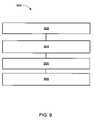
- FIG. 8therein is shown an enlarged perspective view of a number of inner leads 802 and a number of outer leads 804 .
- the number of inner leads 802is representative of the number of inner leads 104 Shown in FIGS. 1 and 2 , or the number of inner leads 304 shown in FIGS. 3 and 4 .
- the number of outer leads 804is representative of the number of outer leads 106 shown in FIGS. 1 and 2 , or the number of outer leads 306 shown in FIGS. 3 and 4 .
- the number of outer leads 804has a number of extended lead tips 806 , which is representative of the number of extended lead tips 108 shown in FIGS. 1 and 2 , or the number of extended lead tips 308 shown in FIGS. 3 and 4 .
- the number of extended lead tips 806extends inwardly from the number of outer leads 804 to the inner edge of the number of inner leads 802 .
- a number of bonding wires 810is wire bonded between the number of inner leads 802 and a die (not shown), such as the die 200 shown in FIG. 2 , or the die 400 shown in FIG. 4 .
- FIG. 9therein is shown a flow chart of a method 900 for manufacturing a semiconductor package comprising: providing a leadframe comprising: a die attach paddle; a number of inner leads; a number of outer leads; a number of extended lead tips on the number of outer leads to extend the inner edges of the number of outer leads in substantial alignment with the inner edges of the number of inner leads, in a block 902 ; attaching a die to the die attach paddle, in a block 904 ; wire bonding the die to the number of inner leads and the number of outer leads in a block 906 ; and encapsulating the leadframe and the die attach paddle, in a block 908 .
Landscapes
- Engineering & Computer Science (AREA)
- Computer Hardware Design (AREA)
- Microelectronics & Electronic Packaging (AREA)
- Power Engineering (AREA)
- Physics & Mathematics (AREA)
- Condensed Matter Physics & Semiconductors (AREA)
- General Physics & Mathematics (AREA)
- Geometry (AREA)
- Lead Frames For Integrated Circuits (AREA)
Abstract
Description
Claims (9)
Priority Applications (3)
| Application Number | Priority Date | Filing Date | Title |
|---|---|---|---|
| US10/846,171US7060536B2 (en) | 2004-05-13 | 2004-05-13 | Dual row leadframe and fabrication method |
| SG200502390ASG117540A1 (en) | 2004-05-13 | 2005-04-21 | Dual row leadframe and fabrication method |
| US11/379,740US7339258B2 (en) | 2004-05-13 | 2006-04-21 | Dual row leadframe and fabrication method |
Applications Claiming Priority (1)
| Application Number | Priority Date | Filing Date | Title |
|---|---|---|---|
| US10/846,171US7060536B2 (en) | 2004-05-13 | 2004-05-13 | Dual row leadframe and fabrication method |
Related Child Applications (1)
| Application Number | Title | Priority Date | Filing Date |
|---|---|---|---|
| US11/379,740DivisionUS7339258B2 (en) | 2004-05-13 | 2006-04-21 | Dual row leadframe and fabrication method |
Publications (2)
| Publication Number | Publication Date |
|---|---|
| US20050260787A1 US20050260787A1 (en) | 2005-11-24 |
| US7060536B2true US7060536B2 (en) | 2006-06-13 |
Family
ID=35375706
Family Applications (2)
| Application Number | Title | Priority Date | Filing Date |
|---|---|---|---|
| US10/846,171Expired - LifetimeUS7060536B2 (en) | 2004-05-13 | 2004-05-13 | Dual row leadframe and fabrication method |
| US11/379,740Expired - LifetimeUS7339258B2 (en) | 2004-05-13 | 2006-04-21 | Dual row leadframe and fabrication method |
Family Applications After (1)
| Application Number | Title | Priority Date | Filing Date |
|---|---|---|---|
| US11/379,740Expired - LifetimeUS7339258B2 (en) | 2004-05-13 | 2006-04-21 | Dual row leadframe and fabrication method |
Country Status (2)
| Country | Link |
|---|---|
| US (2) | US7060536B2 (en) |
| SG (1) | SG117540A1 (en) |
Cited By (11)
| Publication number | Priority date | Publication date | Assignee | Title |
|---|---|---|---|---|
| US20060192274A1 (en)* | 2004-11-12 | 2006-08-31 | Chippac, Inc | Semiconductor package having double layer leadframe |
| US20070126092A1 (en)* | 2005-12-02 | 2007-06-07 | Advanced Interconnect Technologies Limited, A Corporation Of The Republic Of Mauritius | Leadless semiconductor package and method of manufacture |
| US20070267731A1 (en)* | 2006-05-17 | 2007-11-22 | Punzalan Jeffrey D | Integrated circuit package system with different mold locking features |
| US20080067698A1 (en)* | 2006-09-15 | 2008-03-20 | Stats Chippac Ltd. | Integrated circuit package system with encapsulation lock |
| US20080067639A1 (en)* | 2006-09-15 | 2008-03-20 | Stats Chippac Ltd. | Integrated circuit package system with encapsulation lock |
| US20080067640A1 (en)* | 2006-09-15 | 2008-03-20 | Stats Chippac Ltd. | Integrated circuit package system with encapsulation lock |
| US20080111215A1 (en)* | 2006-11-10 | 2008-05-15 | Stats Chippac Ltd. | Integrated circuit package system |
| US20080111218A1 (en)* | 2006-11-09 | 2008-05-15 | Stats Chippac Ltd. | Integrated circuit package system with encapsulation lock |
| US20080185693A1 (en)* | 2007-02-02 | 2008-08-07 | Punzalan Jeffrey D | Integrated circuit package system with integral inner lead and paddle |
| US20080237816A1 (en)* | 2007-03-30 | 2008-10-02 | Henry Descalzo Bathan | Integrated circuit package system with encapsulating features |
| US20080290481A1 (en)* | 2007-05-25 | 2008-11-27 | Takahiko Kudoh | Semiconductor Device Package Leadframe |
Families Citing this family (9)
| Publication number | Priority date | Publication date | Assignee | Title |
|---|---|---|---|---|
| US7489022B2 (en)* | 2005-08-02 | 2009-02-10 | Viasat, Inc. | Radio frequency over-molded leadframe package |
| US7598599B2 (en)* | 2006-03-09 | 2009-10-06 | Stats Chippac Ltd. | Semiconductor package system with substrate having different bondable heights at lead finger tips |
| KR100780966B1 (en)* | 2006-12-07 | 2007-12-03 | 삼성전자주식회사 | Semiconductor package and manufacturing method thereof |
| US9202777B2 (en)* | 2008-05-30 | 2015-12-01 | Stats Chippac Ltd. | Semiconductor package system with cut multiple lead pads |
| US8796155B2 (en)* | 2008-12-04 | 2014-08-05 | Micron Technology, Inc. | Methods of fabricating substrates |
| US8916957B2 (en)* | 2011-07-20 | 2014-12-23 | Aptos Technology Inc. | Package structure and package process |
| US9196504B2 (en)* | 2012-07-03 | 2015-11-24 | Utac Dongguan Ltd. | Thermal leadless array package with die attach pad locking feature |
| JP7338204B2 (en)* | 2019-04-01 | 2023-09-05 | 富士電機株式会社 | semiconductor equipment |
| CN115799204A (en)* | 2022-12-01 | 2023-03-14 | 日荣半导体(上海)有限公司 | Integrated circuit lead frame unit, integrated circuit lead frame and integrated circuit product |
Citations (4)
| Publication number | Priority date | Publication date | Assignee | Title |
|---|---|---|---|---|
| US20020041010A1 (en)* | 2000-10-06 | 2002-04-11 | Kazutaka Shibata | Semiconductor device and lead frame used therefor |
| US6455922B1 (en)* | 1999-06-30 | 2002-09-24 | Texas Instruments Incorporated | Deformation-absorbing leadframe for semiconductor devices |
| US20020140074A1 (en)* | 2001-03-27 | 2002-10-03 | Wehrly James Douglas | Contact member stacking system and method |
| US6703692B1 (en)* | 2002-01-31 | 2004-03-09 | Linear Technology Corp. | Leadframe with support members |
Family Cites Families (8)
| Publication number | Priority date | Publication date | Assignee | Title |
|---|---|---|---|---|
| US7042068B2 (en)* | 2000-04-27 | 2006-05-09 | Amkor Technology, Inc. | Leadframe and semiconductor package made using the leadframe |
| JP2002118222A (en)* | 2000-10-10 | 2002-04-19 | Rohm Co Ltd | Semiconductor device |
| KR100369393B1 (en)* | 2001-03-27 | 2003-02-05 | 앰코 테크놀로지 코리아 주식회사 | Lead frame and semiconductor package using it and its manufacturing method |
| US6630373B2 (en)* | 2002-02-26 | 2003-10-07 | St Assembly Test Service Ltd. | Ground plane for exposed package |
| US6841854B2 (en)* | 2002-04-01 | 2005-01-11 | Matsushita Electric Industrial Co., Ltd. | Semiconductor device |
| JP2004071801A (en)* | 2002-08-06 | 2004-03-04 | Shinko Electric Ind Co Ltd | Lead frame and its fabricating method |
| US7064420B2 (en)* | 2002-09-30 | 2006-06-20 | St Assembly Test Services Ltd. | Integrated circuit leadframe with ground plane |
| TW200425427A (en)* | 2003-05-02 | 2004-11-16 | Siliconware Precision Industries Co Ltd | Leadframe-based non-leaded semiconductor package and method of fabricating the same |
- 2004
- 2004-05-13USUS10/846,171patent/US7060536B2/ennot_activeExpired - Lifetime
- 2005
- 2005-04-21SGSG200502390Apatent/SG117540A1/enunknown
- 2006
- 2006-04-21USUS11/379,740patent/US7339258B2/ennot_activeExpired - Lifetime
Patent Citations (4)
| Publication number | Priority date | Publication date | Assignee | Title |
|---|---|---|---|---|
| US6455922B1 (en)* | 1999-06-30 | 2002-09-24 | Texas Instruments Incorporated | Deformation-absorbing leadframe for semiconductor devices |
| US20020041010A1 (en)* | 2000-10-06 | 2002-04-11 | Kazutaka Shibata | Semiconductor device and lead frame used therefor |
| US20020140074A1 (en)* | 2001-03-27 | 2002-10-03 | Wehrly James Douglas | Contact member stacking system and method |
| US6703692B1 (en)* | 2002-01-31 | 2004-03-09 | Linear Technology Corp. | Leadframe with support members |
Cited By (26)
| Publication number | Priority date | Publication date | Assignee | Title |
|---|---|---|---|---|
| US20060192274A1 (en)* | 2004-11-12 | 2006-08-31 | Chippac, Inc | Semiconductor package having double layer leadframe |
| US7671451B2 (en) | 2004-11-12 | 2010-03-02 | Chippac, Inc. | Semiconductor package having double layer leadframe |
| US20070126092A1 (en)* | 2005-12-02 | 2007-06-07 | Advanced Interconnect Technologies Limited, A Corporation Of The Republic Of Mauritius | Leadless semiconductor package and method of manufacture |
| US7943431B2 (en)* | 2005-12-02 | 2011-05-17 | Unisem (Mauritius) Holdings Limited | Leadless semiconductor package and method of manufacture |
| US20070267731A1 (en)* | 2006-05-17 | 2007-11-22 | Punzalan Jeffrey D | Integrated circuit package system with different mold locking features |
| US8039947B2 (en)* | 2006-05-17 | 2011-10-18 | Stats Chippac Ltd. | Integrated circuit package system with different mold locking features |
| US8779568B2 (en) | 2006-09-15 | 2014-07-15 | Stats Chippac Ltd. | Integrated circuit package system with encapsulation lock |
| US7919838B2 (en) | 2006-09-15 | 2011-04-05 | Stats Chippac Ltd. | Integrated circuit package system with encapsulation lock and method of manufacture thereof |
| US8093693B2 (en) | 2006-09-15 | 2012-01-10 | Stats Chippac Ltd. | Integrated circuit package system with encapsulation lock |
| US8067271B2 (en) | 2006-09-15 | 2011-11-29 | Stats Chippac Ltd. | Integrated circuit package system with encapsulation lock |
| US20080067640A1 (en)* | 2006-09-15 | 2008-03-20 | Stats Chippac Ltd. | Integrated circuit package system with encapsulation lock |
| US20080067639A1 (en)* | 2006-09-15 | 2008-03-20 | Stats Chippac Ltd. | Integrated circuit package system with encapsulation lock |
| US20100117205A1 (en)* | 2006-09-15 | 2010-05-13 | Byung Tai Do | Integrated circuit package system with encapsulation lock and method of manufacture thereof |
| US20080067698A1 (en)* | 2006-09-15 | 2008-03-20 | Stats Chippac Ltd. | Integrated circuit package system with encapsulation lock |
| US20080111218A1 (en)* | 2006-11-09 | 2008-05-15 | Stats Chippac Ltd. | Integrated circuit package system with encapsulation lock |
| US7582957B2 (en) | 2006-11-09 | 2009-09-01 | Stats Chippac Ltd. | Integrated circuit package system with encapsulation lock |
| US20080111215A1 (en)* | 2006-11-10 | 2008-05-15 | Stats Chippac Ltd. | Integrated circuit package system |
| US7928540B2 (en) | 2006-11-10 | 2011-04-19 | Stats Chippac Ltd. | Integrated circuit package system |
| US20100264529A1 (en)* | 2007-02-02 | 2010-10-21 | Punzalan Jeffrey D | Integrated circuit package system with integral inner lead and paddle and method of manufacture thereof |
| US7777310B2 (en) | 2007-02-02 | 2010-08-17 | Stats Chippac Ltd. | Integrated circuit package system with integral inner lead and paddle |
| US8633062B2 (en) | 2007-02-02 | 2014-01-21 | Stats Chippac Ltd. | Integrated circuit package system with integral inner lead and paddle and method of manufacture thereof |
| US20080185693A1 (en)* | 2007-02-02 | 2008-08-07 | Punzalan Jeffrey D | Integrated circuit package system with integral inner lead and paddle |
| US20080237816A1 (en)* | 2007-03-30 | 2008-10-02 | Henry Descalzo Bathan | Integrated circuit package system with encapsulating features |
| US8207600B2 (en) | 2007-03-30 | 2012-06-26 | Stats Chippac Ltd. | Integrated circuit package system with encapsulating features |
| WO2008147857A1 (en)* | 2007-05-25 | 2008-12-04 | Texas Instruments Incorporated | Semiconductor device package leadframe |
| US20080290481A1 (en)* | 2007-05-25 | 2008-11-27 | Takahiko Kudoh | Semiconductor Device Package Leadframe |
Also Published As
| Publication number | Publication date |
|---|---|
| US20060186515A1 (en) | 2006-08-24 |
| US7339258B2 (en) | 2008-03-04 |
| US20050260787A1 (en) | 2005-11-24 |
| SG117540A1 (en) | 2005-12-29 |
Similar Documents
| Publication | Publication Date | Title |
|---|---|---|
| US7339258B2 (en) | Dual row leadframe and fabrication method | |
| US7598599B2 (en) | Semiconductor package system with substrate having different bondable heights at lead finger tips | |
| US7700404B2 (en) | Large die package structures and fabrication method therefor | |
| US8350380B2 (en) | Method for manufacturing leadframe, packaging method for using the leadframe and semiconductor package product | |
| US7834435B2 (en) | Leadframe with extended pad segments between leads and die pad, and leadframe package using the same | |
| US7413933B2 (en) | Integrated circuit package with leadframe locked encapsulation and method of manufacture therefor | |
| US7863108B2 (en) | Integrated circuit packaging system with etched ring and die paddle and method of manufacture thereof | |
| US6927479B2 (en) | Method of manufacturing a semiconductor package for a die larger than a die pad | |
| US20070176269A1 (en) | Multi-chips module package and manufacturing method thereof | |
| US20070170572A1 (en) | Multichip stack structure | |
| US9202777B2 (en) | Semiconductor package system with cut multiple lead pads | |
| US8536688B2 (en) | Integrated circuit leadframe and fabrication method therefor | |
| US20040188818A1 (en) | Multi-chips module package | |
| US7298026B2 (en) | Large die package and method for the fabrication thereof | |
| US7307352B2 (en) | Semiconductor package having changed substrate design using special wire bonding | |
| US7135760B2 (en) | Moisture resistant integrated circuit leadframe package | |
| US8153478B2 (en) | Method for manufacturing integrated circuit package system with under paddle leadfingers | |
| US6339253B1 (en) | Semiconductor package | |
| EP1944802A2 (en) | Method for manufacturing a leadframe, packaging method for using the leadframe and semiconductor package product | |
| KR100708050B1 (en) | Semiconductor Package | |
| KR20020067100A (en) | semiconductor chip package having exposed inner lead and manufacturing method thereof | |
| KR20040048451A (en) | method for fabricating semiconductor package |
Legal Events
| Date | Code | Title | Description |
|---|---|---|---|
| AS | Assignment | Owner name:ST ASSEMBLY TEST SERVICES LTD., SINGAPORE Free format text:ASSIGNMENT OF ASSIGNORS INTEREST;ASSIGNORS:PUNZALAN, JEFFREY D.;CAPARAS, JOSE ALVIN;KU, JAE HUN;REEL/FRAME:014879/0047 Effective date:20040511 | |
| STCF | Information on status: patent grant | Free format text:PATENTED CASE | |
| CC | Certificate of correction | ||
| FPAY | Fee payment | Year of fee payment:4 | |
| FPAY | Fee payment | Year of fee payment:8 | |
| AS | Assignment | Owner name:CITICORP INTERNATIONAL LIMITED, AS COMMON SECURITY AGENT, HONG KONG Free format text:SECURITY INTEREST;ASSIGNORS:STATS CHIPPAC, INC.;STATS CHIPPAC LTD.;REEL/FRAME:036288/0748 Effective date:20150806 Owner name:STATS CHIPPAC LTD., SINGAPORE Free format text:CHANGE OF NAME;ASSIGNOR:ST ASSEMBLY TEST SERVICES LTD.;REEL/FRAME:036286/0590 Effective date:20040608 Owner name:CITICORP INTERNATIONAL LIMITED, AS COMMON SECURITY Free format text:SECURITY INTEREST;ASSIGNORS:STATS CHIPPAC, INC.;STATS CHIPPAC LTD.;REEL/FRAME:036288/0748 Effective date:20150806 | |
| AS | Assignment | Owner name:STATS CHIPPAC PTE. LTE., SINGAPORE Free format text:CHANGE OF NAME;ASSIGNOR:STATS CHIPPAC LTD.;REEL/FRAME:038378/0400 Effective date:20160329 | |
| MAFP | Maintenance fee payment | Free format text:PAYMENT OF MAINTENANCE FEE, 12TH YEAR, LARGE ENTITY (ORIGINAL EVENT CODE: M1553) Year of fee payment:12 | |
| AS | Assignment | Owner name:STATS CHIPPAC PTE. LTD. FORMERLY KNOWN AS STATS CHIPPAC LTD., SINGAPORE Free format text:RELEASE BY SECURED PARTY;ASSIGNOR:CITICORP INTERNATIONAL LIMITED, AS COMMON SECURITY AGENT;REEL/FRAME:052950/0497 Effective date:20190503 Owner name:STATS CHIPPAC, INC., CALIFORNIA Free format text:RELEASE BY SECURED PARTY;ASSIGNOR:CITICORP INTERNATIONAL LIMITED, AS COMMON SECURITY AGENT;REEL/FRAME:052950/0497 Effective date:20190503 | |
| AS | Assignment | Owner name:STATS CHIPPAC PTE. LTD., DISTRICT OF COLUMBIA Free format text:CORRECTIVE ASSIGNMENT TO CORRECT THE ASSIGNEE'S NAME PREVIOUSLY RECORDED AT REEL: 038378 FRAME: 0400. ASSIGNOR(S) HEREBY CONFIRMS THE ASSIGNMENT;ASSIGNOR:STATS CHIPPAC LTD.;REEL/FRAME:064806/0593 Effective date:20160329 |