US7056806B2 - Microfeature workpiece processing apparatus and methods for controlling deposition of materials on microfeature workpieces - Google Patents
Microfeature workpiece processing apparatus and methods for controlling deposition of materials on microfeature workpiecesDownload PDFInfo
- Publication number
- US7056806B2 US7056806B2US10/665,099US66509903AUS7056806B2US 7056806 B2US7056806 B2US 7056806B2US 66509903 AUS66509903 AUS 66509903AUS 7056806 B2US7056806 B2US 7056806B2
- Authority
- US
- United States
- Prior art keywords
- enclosure
- pressure
- flow rate
- gas
- precursor gas
- Prior art date
- Legal status (The legal status is an assumption and is not a legal conclusion. Google has not performed a legal analysis and makes no representation as to the accuracy of the status listed.)
- Expired - Fee Related, expires
Links
- 238000000034methodMethods0.000titleclaimsabstractdescription204
- 239000000463materialSubstances0.000titleclaimsabstractdescription23
- 230000008021depositionEffects0.000titledescription15
- 239000002243precursorSubstances0.000claimsabstractdescription117
- 238000010926purgeMethods0.000claimsabstractdescription109
- 230000001965increasing effectEffects0.000claimsabstractdescription29
- 238000000151depositionMethods0.000claimsabstractdescription24
- 239000007789gasSubstances0.000claimsdescription159
- 239000002356single layerSubstances0.000claimsdescription12
- IJGRMHOSHXDMSA-UHFFFAOYSA-NAtomic nitrogenChemical compoundN#NIJGRMHOSHXDMSA-UHFFFAOYSA-N0.000claimsdescription10
- 230000007423decreaseEffects0.000claimsdescription10
- 229910052757nitrogenInorganic materials0.000claimsdescription5
- NRTOMJZYCJJWKI-UHFFFAOYSA-NTitanium nitrideChemical compound[Ti]#NNRTOMJZYCJJWKI-UHFFFAOYSA-N0.000claimsdescription2
- 230000003247decreasing effectEffects0.000claimsdescription2
- RTAQQCXQSZGOHL-UHFFFAOYSA-NTitaniumChemical compound[Ti]RTAQQCXQSZGOHL-UHFFFAOYSA-N0.000claims1
- 229910052719titaniumInorganic materials0.000claims1
- 239000010936titaniumSubstances0.000claims1
- 238000000231atomic layer depositionMethods0.000description23
- 235000012431wafersNutrition0.000description20
- 239000010410layerSubstances0.000description15
- 239000012071phaseSubstances0.000description12
- 238000004519manufacturing processMethods0.000description10
- 238000005229chemical vapour depositionMethods0.000description7
- 238000009792diffusion processMethods0.000description7
- 238000006243chemical reactionMethods0.000description6
- 239000007787solidSubstances0.000description6
- 229910003074TiCl4Inorganic materials0.000description4
- 230000008901benefitEffects0.000description4
- 239000007795chemical reaction productSubstances0.000description4
- 238000007736thin film deposition techniqueMethods0.000description4
- XJDNKRIXUMDJCW-UHFFFAOYSA-Jtitanium tetrachlorideChemical compoundCl[Ti](Cl)(Cl)ClXJDNKRIXUMDJCW-UHFFFAOYSA-J0.000description4
- 229920006395saturated elastomerPolymers0.000description3
- 239000004065semiconductorSubstances0.000description3
- 239000000758substrateSubstances0.000description3
- 239000010409thin filmSubstances0.000description3
- XUIMIQQOPSSXEZ-UHFFFAOYSA-NSiliconChemical compound[Si]XUIMIQQOPSSXEZ-UHFFFAOYSA-N0.000description2
- 230000003466anti-cipated effectEffects0.000description2
- 238000010923batch productionMethods0.000description2
- 238000005137deposition processMethods0.000description2
- 238000010586diagramMethods0.000description2
- 238000000605extractionMethods0.000description2
- 230000000977initiatory effectEffects0.000description2
- 238000004377microelectronicMethods0.000description2
- 239000002052molecular layerSubstances0.000description2
- 229910052710siliconInorganic materials0.000description2
- 239000010703siliconSubstances0.000description2
- 238000001179sorption measurementMethods0.000description2
- 238000012876topographyMethods0.000description2
- JBRZTFJDHDCESZ-UHFFFAOYSA-NAsGaChemical compound[As]#[Ga]JBRZTFJDHDCESZ-UHFFFAOYSA-N0.000description1
- 229910001218Gallium arsenideInorganic materials0.000description1
- ATJFFYVFTNAWJD-UHFFFAOYSA-NTinChemical compound[Sn]ATJFFYVFTNAWJD-UHFFFAOYSA-N0.000description1
- 230000002411adverseEffects0.000description1
- 239000011248coating agentSubstances0.000description1
- 238000000576coating methodMethods0.000description1
- 230000006835compressionEffects0.000description1
- 238000007906compressionMethods0.000description1
- 238000012864cross contaminationMethods0.000description1
- 238000013500data storageMethods0.000description1
- 230000002939deleterious effectEffects0.000description1
- 230000001627detrimental effectEffects0.000description1
- -1e.g.Substances0.000description1
- 238000005516engineering processMethods0.000description1
- 230000002708enhancing effectEffects0.000description1
- 230000001747exhibiting effectEffects0.000description1
- 239000010408filmSubstances0.000description1
- 239000007792gaseous phaseSubstances0.000description1
- 239000011521glassSubstances0.000description1
- 229910052736halogenInorganic materials0.000description1
- 238000010438heat treatmentMethods0.000description1
- 239000000203mixtureSubstances0.000description1
- 238000012986modificationMethods0.000description1
- 230000004048modificationEffects0.000description1
- 239000000047productSubstances0.000description1
- 238000005086pumpingMethods0.000description1
- 239000012713reactive precursorSubstances0.000description1
- 239000011343solid materialSubstances0.000description1
- 230000000087stabilizing effectEffects0.000description1
Images


Classifications
- C—CHEMISTRY; METALLURGY
- C23—COATING METALLIC MATERIAL; COATING MATERIAL WITH METALLIC MATERIAL; CHEMICAL SURFACE TREATMENT; DIFFUSION TREATMENT OF METALLIC MATERIAL; COATING BY VACUUM EVAPORATION, BY SPUTTERING, BY ION IMPLANTATION OR BY CHEMICAL VAPOUR DEPOSITION, IN GENERAL; INHIBITING CORROSION OF METALLIC MATERIAL OR INCRUSTATION IN GENERAL
- C23C—COATING METALLIC MATERIAL; COATING MATERIAL WITH METALLIC MATERIAL; SURFACE TREATMENT OF METALLIC MATERIAL BY DIFFUSION INTO THE SURFACE, BY CHEMICAL CONVERSION OR SUBSTITUTION; COATING BY VACUUM EVAPORATION, BY SPUTTERING, BY ION IMPLANTATION OR BY CHEMICAL VAPOUR DEPOSITION, IN GENERAL
- C23C16/00—Chemical coating by decomposition of gaseous compounds, without leaving reaction products of surface material in the coating, i.e. chemical vapour deposition [CVD] processes
- C23C16/44—Chemical coating by decomposition of gaseous compounds, without leaving reaction products of surface material in the coating, i.e. chemical vapour deposition [CVD] processes characterised by the method of coating
- C23C16/455—Chemical coating by decomposition of gaseous compounds, without leaving reaction products of surface material in the coating, i.e. chemical vapour deposition [CVD] processes characterised by the method of coating characterised by the method used for introducing gases into reaction chamber or for modifying gas flows in reaction chamber
- C23C16/45523—Pulsed gas flow or change of composition over time
- C23C16/45525—Atomic layer deposition [ALD]
- C23C16/45527—Atomic layer deposition [ALD] characterized by the ALD cycle, e.g. different flows or temperatures during half-reactions, unusual pulsing sequence, use of precursor mixtures or auxiliary reactants or activations
- C—CHEMISTRY; METALLURGY
- C23—COATING METALLIC MATERIAL; COATING MATERIAL WITH METALLIC MATERIAL; CHEMICAL SURFACE TREATMENT; DIFFUSION TREATMENT OF METALLIC MATERIAL; COATING BY VACUUM EVAPORATION, BY SPUTTERING, BY ION IMPLANTATION OR BY CHEMICAL VAPOUR DEPOSITION, IN GENERAL; INHIBITING CORROSION OF METALLIC MATERIAL OR INCRUSTATION IN GENERAL
- C23C—COATING METALLIC MATERIAL; COATING MATERIAL WITH METALLIC MATERIAL; SURFACE TREATMENT OF METALLIC MATERIAL BY DIFFUSION INTO THE SURFACE, BY CHEMICAL CONVERSION OR SUBSTITUTION; COATING BY VACUUM EVAPORATION, BY SPUTTERING, BY ION IMPLANTATION OR BY CHEMICAL VAPOUR DEPOSITION, IN GENERAL
- C23C16/00—Chemical coating by decomposition of gaseous compounds, without leaving reaction products of surface material in the coating, i.e. chemical vapour deposition [CVD] processes
- C23C16/22—Chemical coating by decomposition of gaseous compounds, without leaving reaction products of surface material in the coating, i.e. chemical vapour deposition [CVD] processes characterised by the deposition of inorganic material, other than metallic material
- C23C16/30—Deposition of compounds, mixtures or solid solutions, e.g. borides, carbides, nitrides
- C23C16/34—Nitrides
- C—CHEMISTRY; METALLURGY
- C23—COATING METALLIC MATERIAL; COATING MATERIAL WITH METALLIC MATERIAL; CHEMICAL SURFACE TREATMENT; DIFFUSION TREATMENT OF METALLIC MATERIAL; COATING BY VACUUM EVAPORATION, BY SPUTTERING, BY ION IMPLANTATION OR BY CHEMICAL VAPOUR DEPOSITION, IN GENERAL; INHIBITING CORROSION OF METALLIC MATERIAL OR INCRUSTATION IN GENERAL
- C23C—COATING METALLIC MATERIAL; COATING MATERIAL WITH METALLIC MATERIAL; SURFACE TREATMENT OF METALLIC MATERIAL BY DIFFUSION INTO THE SURFACE, BY CHEMICAL CONVERSION OR SUBSTITUTION; COATING BY VACUUM EVAPORATION, BY SPUTTERING, BY ION IMPLANTATION OR BY CHEMICAL VAPOUR DEPOSITION, IN GENERAL
- C23C16/00—Chemical coating by decomposition of gaseous compounds, without leaving reaction products of surface material in the coating, i.e. chemical vapour deposition [CVD] processes
- C23C16/44—Chemical coating by decomposition of gaseous compounds, without leaving reaction products of surface material in the coating, i.e. chemical vapour deposition [CVD] processes characterised by the method of coating
- C23C16/455—Chemical coating by decomposition of gaseous compounds, without leaving reaction products of surface material in the coating, i.e. chemical vapour deposition [CVD] processes characterised by the method of coating characterised by the method used for introducing gases into reaction chamber or for modifying gas flows in reaction chamber
- C23C16/45523—Pulsed gas flow or change of composition over time
- C23C16/45525—Atomic layer deposition [ALD]
- C23C16/45544—Atomic layer deposition [ALD] characterized by the apparatus
- C23C16/45546—Atomic layer deposition [ALD] characterized by the apparatus specially adapted for a substrate stack in the ALD reactor
Definitions
- the present inventionis related to equipment and methods for processing microfeature workpieces, e.g., semiconductor wafers. Aspects of the invention have particular utility in connection with batch deposition of materials on microfeature workpieces by atomic layer deposition.
- Thin film deposition techniquesare widely used in the manufacturing of microfeatures to form a coating on a workpiece that closely conforms to the surface topography.
- the size of the individual components in the devices on a waferis constantly decreasing, and the number of layers in the devices is increasing.
- the density of components and the aspect ratios of depressionse.g., the ratio of the depth to the size of the opening
- the size of such wafersis also increasing to provide more real estate for forming more dies (i.e., chips) on a single wafer.
- Many fabricatorsare currently transitioning from 200 mm to 300 mm workpieces, and even larger workpieces will likely be used in the future.
- Thin film deposition techniquesaccordingly strive to produce highly uniform conformal layers that cover the sidewalls, bottoms, and corners in deep depressions that have very small openings.
- CVDchemical vapor deposition
- one or more precursors that are capable of reacting to form a solid thin filmare mixed in a gas or vapor state, and then the precursor mixture is presented to the surface of the workpiece.
- the surface of the workpiececatalyzes the reaction between the precursors to form a solid thin film at the workpiece surface.
- a common way to catalyze the reaction at the surface of the workpieceis to heat the workpiece to a temperature that causes the reaction.
- CVD techniquesare useful in many applications, they also have several drawbacks. For example, if the precursors are not highly reactive, then a high workpiece temperature is needed to achieve a reasonable deposition rate. Such high temperatures are not typically desirable because heating the workpiece can be detrimental to the structures and other materials already formed on the workpiece. Implanted or doped materials, for example, can migrate within silicon workpieces at higher temperatures. On the other hand, if more reactive precursors are used so that the workpiece temperature can be lower, then reactions may occur prematurely in the gas phase before reaching the intended surface of the workpiece. This is undesirable because the film quality and uniformity may suffer, and also because it limits the types of precursors that can be used.
- Atomic layer depositionis another thin film deposition technique.
- FIGS. 1A and 1Bschematically illustrate the basic operation of ALD processes.
- a layer of gas molecules Acoats the surface of a workpiece W.
- the layer of A moleculesis formed by exposing the workpiece W to a precursor gas containing A molecules, and then purging the chamber with a purge gas to remove excess A molecules.
- This processcan form a monolayer of A molecules on the surface of the workpiece W because the A molecules at the surface are held in place during the purge cycle by physical adsorption forces at moderate temperatures or chemisorption forces at higher temperatures.
- the layer of A moleculesis then exposed to another precursor gas containing B molecules.
- the A moleculesreact with the B molecules to form an extremely thin layer of solid material C on the workpiece W.
- the chamberis then purged again with a purge gas to remove excess B molecules.
- FIG. 2illustrates the stages of one cycle for forming a thin solid layer using ALD techniques.
- a typical cycleincludes (a) exposing the workpiece to the first precursor A, (b) purging excess A molecules, (c) exposing the workpiece to the second precursor B, and then (d) purging excess B molecules.
- the purge processtypically comprises introducing a purge gas, which is substantially non-reactive with either precursor, and exhausting the purge gas and excess precursor from the reaction chamber in a pumping step.
- several cyclesare repeated to build a thin film on a workpiece having the desired thickness. For example, each cycle may form a layer having a thickness of approximately 0.5–1.0 ⁇ , and thus it takes approximately 60–120 cycles to form a solid layer having a thickness of approximately 60 ⁇ .
- ALD processinghas a relatively low throughput compared to CVD techniques. For example, ALD processing typically takes several seconds to perform each A-purge-B-purge cycle. This results in a total process time of several minutes to form a single thin layer of only 60 ⁇ . In contrast to ALD processing, CVD techniques only require about one minute to form a 60 ⁇ thick layer. In single-wafer processing chambers, ALD processes can be 500%–2000% longer than corresponding single-wafer CVD processes. The low throughput of existing single-wafer ALD techniques limits the utility of the technology in its current state because ALD may be a bottleneck in the overall manufacturing process.
- One promising solution to increase the throughput of ALD processingis processing a plurality of wafers (e.g., 20–250) simultaneously in a batch process.
- a plurality of waferse.g., 20–250
- batch processestypically stack the plurality of wafers in a wafer holder that is positioned in an enclosure of a processing system.
- the wafersare typically held in a relatively close spaced-apart relationship. Unfortunately, this close spacing between adjacent wafers hinders the flow of gas adjacent the surface of the wafer, particularly adjacent the center of each wafer.
- a gas “showerhead”will be spaced in relatively close, parallel proximity with substantially the entirety of the wafer surface. This facilitates thorough, effective purging of the excess precursors A and B.
- gasis typically introduced to flow longitudinally alongside the wafer holder. As a consequence, gas exchange between the wafers takes place, in large part, by gas diffusion rather than a significant flow rate of gas across the wafer surface.
- conventional batch ALD processingtypically involves introducing a significant quantity of a purge gas to dilute the remaining precursor, then drawing a vacuum on the enclosure to remove the diluted gas. Unfortunately, this addition of excess purge gas and subsequent pump-down can take a relatively long period of time, further reducing the throughput of the batch ALD processing system.
- FIGS. 1A and 1Bare schematic cross-sectional views of stages in ALD processing in accordance with the prior art.
- FIG. 2is a graph illustrating a cycle for forming a layer using ALD techniques in accordance with the prior art.
- FIG. 3is a schematic cross-sectional view of a microfeature workpiece processing system in accordance with an embodiment of the invention.
- FIG. 4is a schematic flow diagram illustrating aspects of a method in accordance with one embodiment of the invention.
- FIG. 5is a flow diagram schematically illustrating aspects of one embodiment of the pump/purge steps in FIG. 4 .
- FIG. 6is a graph schematically illustrating gas pressures and flow rates in accordance with one particular embodiment of the invention.
- FIG. 7is a graph schematically illustrating partial pressure of a precursor gas during various pump and/or purge processes.
- microfeature workpiece holderssystems including processing chambers, and methods for depositing materials onto microfeature workpieces. Many specific details of the invention are described below with reference to reactors for depositing materials onto microfeature workpieces.
- microfeature workpieceis used throughout to include substrates upon which and/or in which microelectronic devices, micromechanical devices, data storage elements, read/write components, and other devices are fabricated.
- microfeature workpiecescan be semiconductor wafers such as silicon or gallium arsenide wafers, glass substrates, insulative substrates, and many other types of materials.
- the microfeature workpiecestypically have submicron features with dimensions of 0.05 microns or greater.
- gasis used throughout to include any form of matter that has no fixed shape and will conform in volume to the space available, which specifically includes vapors (i.e., a gas having a temperature less than the critical temperature so that it may be liquefied or solidified by compression at a constant temperature).
- vaporsi.e., a gas having a temperature less than the critical temperature so that it may be liquefied or solidified by compression at a constant temperature.
- One embodiment of the inventionprovides a method of depositing a material on a microfeature workpiece.
- a plurality of microfeature workpiecesare positioned in a spaced relationship within an enclosure.
- a flow of a first precursor gasis introduced to the enclosure at a first enclosure pressure.
- the flow of the first precursoris terminated and pressure within the enclosure is reduced to a second enclosure pressure while introducing a flow of a purge gas at a first flow rate.
- the processing systemhas a base pressure at the first flow rate.
- a difference between the second enclosure pressure and the first enclosure pressureis at least 90 percent of the difference between the base pressure and the first enclosure pressure.
- the flow rate of the purge gasis increased to a second flow rate and the pressure within the enclosure is increased to a third enclosure pressure.
- a flow of a second precursor gasis introduced to the enclosure at a fourth enclosure pressure.
- the third and fourth enclosure pressuresmay be substantially the same, with any difference between the third and fourth enclosure pressures being about 0–10 percent of the fourth enclosure pressure.
- a method in accordance with another embodiment of the inventionmay also be used to deposit a material on a microfeature workpiece.
- a plurality of microfeature workpieceseach of which has a surface, is positioned within an enclosure.
- the surfaces of the microfeature workpiecesare exposed to a first precursor gas at a first enclosure pressure to allow at least a monolayer of the first precursor gas to be adsorbed on the surfaces of the microfeature workpieces.
- Pressure within the enclosureis reduced to a second, lower enclosure pressure via a pump-down process.
- the pump-down processcomprises withdrawing gas from the enclosure, e.g., with a vacuum, while introducing a purge gas at a first flow rate of no greater than about 250 sccm for a first period of time.
- This pump-down processreduces the partial pressure of the first precursor gas within the enclosure.
- the enclosureis purged in a purge process that includes introducing the purge gas at a second flow rate of at least about 1000 sccm for a second period of time and allowing the enclosure pressure to increase to a third enclosure pressure that is greater than the second enclosure pressure.
- the surfaces of the microfeature workpiecesmay be exposed to a second precursor gas at a fourth enclosure pressure.
- the third and fourth enclosure pressuresmay be substantially the same, with any difference between the third and fourth enclosure pressures desirably being about 0–10 percent of the fourth enclosure pressure.
- a microfeature workpiece processing systemthat includes an enclosure, a gas supply, a vacuum, and a programmable controller.
- the enclosureis adapted to receive a plurality of microfeature workpieces for simultaneous treatment.
- the gas supplyis adapted to selectively deliver a first gaseous precursor, a second gaseous precursor, and a purge gas to the enclosure.
- the programmable controlleris operatively coupled to the gas supply and the vacuum, and the controller may be programmed to carry out one of the aforementioned methods or methods in accordance with other aspects of the invention.
- the first sectiondiscusses microfeature workpiece processing systems in accordance with selected embodiments of the invention.
- the second sectionoutlines methods in accordance with other aspects of the invention.
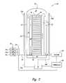
- FIG. 3schematically illustrates a reactor 10 in accordance with one embodiment of the invention.
- This reactor 10includes a processing enclosure 20 coupled to a gas supply 30 and a vacuum 40 .
- the processing enclosure 20generally includes an outer wall 22 and an annular liner 24 .
- a platform 60seals against the outer wall or some other part of the processing enclosure 20 to define a deposition chamber 25 .
- the liner 24functionally divides the deposition chamber 25 into a main chamber 28 and an annular exhaust 26 .
- microfeature workpieces We.g., semiconductor wafers
- a plurality of microfeature workpieces Ware held in the processing enclosure 20 in a workpiece holder 70 .
- FIG. 3is merely schematic in nature and any number (e.g., 20–250) of workpieces W may be held in the workpiece holder 70 for simultaneous batch processing.
- the reactor 10also includes at least one heat source to heat the workpieces W and maintain them at the desired temperature.
- the heat source in FIG. 3is typified as a radiant heater 50 comprising a series of radiant heat panels 50 a and 50 b arranged about a circumference of the enclosure 20 to evenly heat the workpieces W.
- these heat panels 50 a–bcomprise quartz-halogen lamps or other types of radiative heat sources.
- other types of heat sourcesmay be employed.
- the heater 50may also include a power supply 52 that is coupled to the first heat panel 50 a by a first power line 54 a and to the second heat panel 50 b by a second power line 54 b.
- Gasis introduced from the gas supply 30 to the deposition chamber 25 by a gas line 32 and an inlet 36 .
- the inlet 36directs a flow of gas into the main chamber 28 of the deposition chamber 25 .
- gas introduced via the gas inlet 36will flow through the main chamber 28 , outwardly into the annular exhaust 26 , and out of the deposition chamber 25 .
- a valve assembly 34 in the gas line 32may be operated by a controller 90 to selectively deliver gases to the deposition chamber 25 during the deposition phase.
- the controller 90comprises a computer having a programmable processor programmed to control operation of the reactor 10 to deposit material on the workpieces W in accordance with one or more of the methods outlined below.
- the controller 90may be coupled to the vacuum 40 to control its operation.
- the controller 90may also be operatively connected to the heater 50 , e.g., via the power supply 52 , to control the temperature of the workpieces W.
- the reactor 10is adapted to carry out an ALD process employing multiple precursors.
- the gas supply 30 in such embodimentscan include a plurality of separate gas sources 31 a–c , and the valve assembly 34 may have a plurality of valves.
- the gas supply 30may include one or more gaseous precursors capable of reacting to deposit titanium nitride.
- the first gas source 31 ais adapted to deliver TiCl 4
- the second gas source 31 bis adapted to deliver NH 3
- the third gas source 31 cis adapted to deliver a flow of a purge gas, e.g., nitrogen.
- FIGS. 4 and 5schematically illustrate aspects of a method of depositing a material on surfaces of a batch of microfeature workpieces in accordance with one embodiment of the invention; FIG. 4 provides an overview, whereas FIG. 5 provides details of certain aspects of FIG. 4 .
- the workpiece manufacturing process 100may be initiated by positioning the workpieces W in the enclosure 20 of an ALD reactor 10 or other processing system (process 105 ).
- process 110the ambient atmosphere that entered the main chamber 25 of the enclosure 20 may be withdrawn, e.g., by means of the vacuum 40 and a flow of an inert purge gas (e.g., nitrogen from the third gas source 31 c of the gas supply 30 ).
- an inert purge gase.g., nitrogen from the third gas source 31 c of the gas supply 30 .
- the workpieces Wmay also be heated to the desired process temperature by the heaters 50 .
- a flow of the first precursor gasmay be initiated in process 115 and terminated in process 120 .
- Thiswill deliver a pulse of the first precursor gas into the deposition chamber 25 , exposing a surface of each of the workpieces W in the deposition chamber 25 to the first precursor.
- the first precursormay be at least chemisorbed on the workpiece W. Theoretically, such chemisorption will form a monolayer that is uniformly one molecule thick on the entire surface of the workpiece W. Such a monolayer may be referred to as a saturated monolayer. As a practical matter, in some circumstances some minor portions of the workpiece surface may not chemisorb a molecule of the precursor.
- a substantially saturated monolayeris a monolayer that will yield a deposited layer exhibiting the requisite quality and/or performance parameters.
- an excess of the first precursor gasis typically delivered to the processing enclosure 20 .
- This excess first precursor gasis desirably removed from the vicinity of the workpiece surface prior to introduction of the second precursor gas.
- Inadequate removal of the first precursor gas prior to introduction of the second precursor gasmay result in a gaseous phase reaction between the precursors that yields a material that is less conformal to the topography of the workpiece surface or otherwise adversely affects the quality of the deposited material. Consequently, in the manufacturing process 100 of FIG. 4 , a pump/purge process 200 (detailed below) is carried out before introducing the second precursor gas to the enclosure 20 .
- a flow of the second precursor gasmay be initiated in process 130 to deliver a pulse of the second precursor gas to the enclosure 20 .
- This second precursormay chemisorb on the first monolayer of the first precursor and/or react with the monolayer to form a reaction product.
- This reaction productis typically one or no more than a few molecules thick, yielding a very thin, highly conformal nanolayer reaction product.
- the flow of the second precursor gasmay be terminated in process 135 and a pump/purge process 200 may again be performed.
- This series of first precursor—pump/purge—second precursor—pump/purge processesmay be considered one ALD cycle adapted to deposit a single nanolayer of material.
- the ALD processmay need to be repeated a number of times to deposit a layer of material having an appropriate thickness.
- the manufacturing process 100 of FIG. 4may thus include a decision process 140 that decides whether the layer deposited on the microfeature workpieces W is thick enough. In many circumstances, this decision will comprise determining whether a fixed number of deposition cycles, which has been empirically determined to deposit an adequate thickness, has been performed. If a sufficient thickness has not been deposited, the manufacturing process 100 may return to process 115 to deposit another thickness of the reaction product. If the thickness is determined in process 140 to be sufficient, though, the workpieces W may be removed from the enclosure 20 in process 145 .
- FIG. 5schematically illustrates the pump/purge process 200 of FIG. 4 in greater detail.
- This pump/purge process 200generally includes a pump process 210 and a purge process 220 .
- the pump process 210may include introducing a flow of purge gas at a first flow rate (process 212 ) and withdrawing gas from the enclosure 20 until a target pressure is reached (process 214 ). If the vacuum system 40 of the reactor 10 is sufficiently robust, it may be possible to omit the flow of purge gas in process 212 and instead merely withdraw gas from the enclosure 20 with the vacuum 40 in process 214 . This will reduce the pressure within the enclosure 20 more rapidly, reducing the time necessary for the pump process 210 . For many commercial reactors 10 , however, it may be advantageous to continue a flow of purge gas at a relatively low flow rate to reduce the chances of any backflow from or cross-contamination in the vacuum 40 .
- the first flow rate suitable in process 212will depend in part on the design of the reactor 10 , including its size and geometry, and the precursor being removed. In many commercial applications, though, a first flow rate of no greater than about 250 standard cubic centimeters per minute (sccm) will suffice. A flow rate of 0–250 sccm will be appropriate for most applications, but a flow rate of 50–250 sccm, e.g., 50–100 sccm, is preferred for select embodiments.
- the particular embodiment illustrated in FIG. 5shows the introduction of the purge gas in process 212 before withdrawing gas from the enclosure in process 214 . In other embodiments, the order of processes 212 and 214 may be reversed or processes 212 and 214 may start and end simultaneously.
- This purge process 220includes increasing the flow of purge gas to a second flow rate in process 222 and increasing pressure in the enclosure 20 to a process pressure 224 that is higher than the target pressure in process 214 .
- the second flow rate in process 222is at least about four times the first flow rate (process 212 ), though this multiple may be significantly higher. It is anticipated that a second flow rate of at least 1000 sccm will be best in most circumstances. In embodiments employing commercial-scale batch ALD reactors 10 , a second flow rate of no less than 2000 sccm may be advantageous.
- FIGS. 4 and 5provide an overview of the manufacturing process 100 .
- FIG. 6provides a schematic illustration of one particular implementation of the manufacturing process 100 that highlights some of the aspects and advantages of select embodiments of the invention.
- the upper graph of FIG. 6illustrates the pressure in the processing enclosure 20 over the course of part of the manufacturing process 100 .
- the bottom graph of FIG. 6is a schematic plot of the flow rate of a purge gas, a first precursor gas, and a second precursor gas as a function of time. The time scale in both graphs of FIG. 6 is the same.
- the timeline of FIG. 6starts with the initiation of the flow of the first precursor gas in process 115 of FIG. 4 .
- the flow of the first precursor gaswill continue until it is terminated in process 120 , whereupon the pump/purge process 200 may begin.
- the pressure in the main chamber 28 of the enclosure 20may remain substantially constant at a selected process pressure P during the first precursor gas pulse.
- the process pressure Pwill vary depending on the nature of the deposition process being carried out, e.g., the nature of the first and second precursor gases, the temperature of the workpieces W, the volume and dimensions of the enclosure 20 , and other operating parameters.
- the pump/purge process 200includes a pump-down process 210 and a purge process 220 .
- the flow of purge gasmay be relatively low, e.g., 50–100 sccm.
- the vacuum 40activated, the pressure in the main chamber 28 of the enclosure will drop fairly rapidly, as suggested by curve X in the upper graph of FIG. 6 .
- the main chamber 28 of the enclosure 20will have a substantially steady-state lower pressure identified in FIG. 6 as base pressure B.
- the flow rate of the purge gasis increased and the pressure within the main chamber 28 of the enclosure 20 is allowed to increase (curve Y).
- the enclosure pressure at the end of the purge process 220is similar to the process pressure P at which the workpieces W will be exposed to the second precursor gas.
- a difference between the enclosure pressure at the end of the purge process 220 and the desired process pressure P at which the workpieces W will be exposed to the second precursor gasis about 0–10% of the process pressure P.
- the pressure in the enclosuremay slightly exceed the process pressure P, but be brought back down to the process pressure P by the end of the pump/purge process 200 .
- the controller 90is likely to overshoot the desired process pressure P before stabilizing the enclosure pressure. Overshooting the process pressure P with the flow of the second precursor can introduce undesirable variations in the exposure of the workpieces W to the second precursor gas from one cycle to the next.
- the enclosure pressuremay overshoot the process pressure P during the purge process 220 , but the enclosure pressure may be substantially stabilized at the process pressure P before the flow of the second precursor gas is initiated in process 130 . This can enhance uniformity of the process from one cycle to the next.
- One objective of the pump/purge process 200is to reduce the concentration of any excess, nonadsorbed precursor gas in at least the main chamber 28 of the enclosure 20 to an acceptable level.
- the first precursor—pump/purge—second precursor—pump/purge cycletypically must be repeated numerous times to deposit a suitable thickness of material on the surfaces of the workpieces W. Reducing the time of the pump/purge process 200 , therefore, can materially decrease the time needed to reach the suitable material thickness.
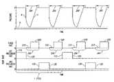
- FIG. 7is a schematic graph comparing the expected concentration of a precursor, expressed as a partial pressure of the precursor in the enclosure, during a purge process 220 only, during a pump-down process 210 only, and during a pump/purge process 200 in accordance with embodiments of the invention.
- the process pressure P at which the pump/purge process 200 is initiatedis arbitrarily set at 1 (i.e., 0 on the log scale of FIG. 7 ).
- curve 320 awhich is generally linear and has a relatively constant first slope S 1 .
- the slope S 1will vary with a number of factors, including the geometry of the enclosure 20 , the relative spacing of the workpieces W, and the rate at which the vacuum withdraws gas from the enclosure. All other factors being equal, though, the slope S 1 generally will increase (i.e., the partial pressure will drop more quickly) with increasing flow rates of purge gas into the enclosure. It should be recognized that curve 320 a is stylized and the partial pressure of the precursor may deviate noticeably from this relatively straight line, particularly at higher purge gas flow rates or higher vacuum extraction rates.
- One advantage of the pump-down process 210is that the partial pressure of the precursor drops off rapidly in the first phase 310 to quickly reduce the partial pressure below a level that promotes further adsorption. This facilitates more precise control over the time the workpieces W are exposed to material concentrations of the precursor.
- the pump/purge process 200 illustrated in FIGS. 4–6is expected to achieve benefits of both the pump-down process 210 and the purge process 220 , yet reduce the total time needed to reduce the concentration of precursor in the enclosure to an acceptable level before introducing the next precursor.
- the pump-down process 210continues until the enclosure pressure reaches the base pressure B, taking advantage of the rapid decrease in partial pressure of the precursor in the first phase 310 of the pump-down. Rather than continuing the second phase 312 of the pump-down process 210 , though, the purge process 220 is initiated promptly after reaching the base pressure B.
- Curve 320 bwhich illustrates the partial pressure of precursor during this purge process 220 , may be a relatively straight line having a slope S 3 that is greater than the slope S 2 of the partial pressure curve in the second phase 312 of the pump-down process 210 . It is anticipated that the slopes S 1 and S 3 of curves 320 a and 320 b , respectively, will be similar and may be substantially the same. As illustrated in FIG. 7 , the increased slope S 3 of curve 320 b compared to slope S 2 during the second pump-down phase 312 will result in a time savings ⁇ t in achieving the same partial pressure of the precursor.
- the pump/purge process 200will allow the concentration of precursor in the main chamber 28 of the enclosure 20 to be reduced to the same level in a shorter period of time than either the pump-down process 210 alone (the solid curve in FIG. 7 ) or the purge process 220 alone (curve 320 a ), increasing throughput of the reactor 10 .
- the purge process 220is initiated promptly upon reaching the base pressure B.
- the pump-down process 210is allowed to continue for a limited time (e.g., 3 seconds or less) thereafter. Because the slope S 2 of the partial pressure curve in the second phase 312 of the pump-down 210 is less than the slope S 3 of curve 320 b , though, delaying initiation of the purge process 220 will reduce the time savings ⁇ t. In other embodiments, the time purge process 220 is initiated before the base pressure B is reached. In the particular embodiment illustrated in FIG.
- the purge process 220starts while the enclosure pressure is slightly higher than the base pressure B achievable in a steady state second phase 312 of the pump-down process 210 .
- the purge process 220is initiated when the difference between the enclosure pressure and the process pressure P is at least 90% of the difference between the base pressure B and the process pressure P.
- the purge process 220is initiated when the difference between the enclosure pressure and the process pressure P is at least 90% of the difference between the base pressure B and the process pressure P, but no later than reaching the base pressure. This will achieve the rapid initial drop-off in partial pressure of the precursor, but initiate the purge process 220 before the less productive second phase 312 of the pump-down process 210 .
- the diffusion rate of any given gaswill vary with pressure, with the diffusion rate increasing as pressure is reduced. Different gases diffuse at different rates, though.
- the diffusion rate D for TiCl 4 in nitrogenis expected to be on the order of 0.032 m 2 /s at an enclosure pressure of about 1 torr, but this diffusion rate will increase to about 0.80 m 2 /s at about 0.04 torr.
- NH 3which may be used as a second precursor with TiCl 4 to deposit TiN, has a diffusion rate D in nitrogen of about 0.088 m 2 /s at about 1 torr, which climbs to about 2.2 m 2 /s at about 0.04 torr. NH 3 , therefore, should diffuse out of the spaces between the workpieces W more readily than TiCl 4 .
- the curves 310 , 312 , 320 a , and 320 b in FIG. 7are expected to follow the same general relationship for most precursor gases, but the precise shapes of the curves (e.g., the slopes S 1-3 ) will vary from one gas to another. If the pump-down process 210 continues for a fixed time in all pump/purge processes 200 in the manufacturing process 100 of FIG. 4 , this time may be selected so the enclosure pressure is reduced by at least 90% of the difference between the base pressure B and the process pressure P for both precursor gases. This may dictate that the enclosure pressure at the end of the pump-down process 210 will vary from one pump/purge process 200 to the next. In another embodiment, the parameters of the pump/purge process 200 may be varied depending on the diffusion characteristics of the precursor gas being purged. This will allow each pump/purge process 200 to be optimized, further enhancing throughput of the reactor 10 without compromising product quality.
Landscapes
- Chemical & Material Sciences (AREA)
- General Chemical & Material Sciences (AREA)
- Chemical Kinetics & Catalysis (AREA)
- Engineering & Computer Science (AREA)
- Materials Engineering (AREA)
- Mechanical Engineering (AREA)
- Metallurgy (AREA)
- Organic Chemistry (AREA)
- Inorganic Chemistry (AREA)
- Chemical Vapour Deposition (AREA)
Abstract
Description
The present invention is related to equipment and methods for processing microfeature workpieces, e.g., semiconductor wafers. Aspects of the invention have particular utility in connection with batch deposition of materials on microfeature workpieces by atomic layer deposition.
Thin film deposition techniques are widely used in the manufacturing of microfeatures to form a coating on a workpiece that closely conforms to the surface topography. In the context of microelectronic components, for example, the size of the individual components in the devices on a wafer is constantly decreasing, and the number of layers in the devices is increasing. As a result, the density of components and the aspect ratios of depressions (e.g., the ratio of the depth to the size of the opening) are increasing. The size of such wafers is also increasing to provide more real estate for forming more dies (i.e., chips) on a single wafer. Many fabricators are currently transitioning from 200 mm to 300 mm workpieces, and even larger workpieces will likely be used in the future. Thin film deposition techniques accordingly strive to produce highly uniform conformal layers that cover the sidewalls, bottoms, and corners in deep depressions that have very small openings.
One widely used thin film deposition technique is chemical vapor deposition (CVD). In a CVD system, one or more precursors that are capable of reacting to form a solid thin film are mixed in a gas or vapor state, and then the precursor mixture is presented to the surface of the workpiece. The surface of the workpiece catalyzes the reaction between the precursors to form a solid thin film at the workpiece surface. A common way to catalyze the reaction at the surface of the workpiece is to heat the workpiece to a temperature that causes the reaction.
Although CVD techniques are useful in many applications, they also have several drawbacks. For example, if the precursors are not highly reactive, then a high workpiece temperature is needed to achieve a reasonable deposition rate. Such high temperatures are not typically desirable because heating the workpiece can be detrimental to the structures and other materials already formed on the workpiece. Implanted or doped materials, for example, can migrate within silicon workpieces at higher temperatures. On the other hand, if more reactive precursors are used so that the workpiece temperature can be lower, then reactions may occur prematurely in the gas phase before reaching the intended surface of the workpiece. This is undesirable because the film quality and uniformity may suffer, and also because it limits the types of precursors that can be used.
Atomic layer deposition (ALD) is another thin film deposition technique.FIGS. 1A and 1B schematically illustrate the basic operation of ALD processes. Referring toFIG. 1A , a layer of gas molecules A coats the surface of a workpiece W. The layer of A molecules is formed by exposing the workpiece W to a precursor gas containing A molecules, and then purging the chamber with a purge gas to remove excess A molecules. This process can form a monolayer of A molecules on the surface of the workpiece W because the A molecules at the surface are held in place during the purge cycle by physical adsorption forces at moderate temperatures or chemisorption forces at higher temperatures. The layer of A molecules is then exposed to another precursor gas containing B molecules. The A molecules react with the B molecules to form an extremely thin layer of solid material C on the workpiece W. The chamber is then purged again with a purge gas to remove excess B molecules.
One drawback of ALD processing is that it has a relatively low throughput compared to CVD techniques. For example, ALD processing typically takes several seconds to perform each A-purge-B-purge cycle. This results in a total process time of several minutes to form a single thin layer of only 60 Å. In contrast to ALD processing, CVD techniques only require about one minute to form a 60 Å thick layer. In single-wafer processing chambers, ALD processes can be 500%–2000% longer than corresponding single-wafer CVD processes. The low throughput of existing single-wafer ALD techniques limits the utility of the technology in its current state because ALD may be a bottleneck in the overall manufacturing process.
One promising solution to increase the throughput of ALD processing is processing a plurality of wafers (e.g., 20–250) simultaneously in a batch process. As suggested in International Publication No. WO 02/095807, the entirety of which is incorporated herein by reference, such batch processes typically stack the plurality of wafers in a wafer holder that is positioned in an enclosure of a processing system. To increase the number of wafers that can be treated at one time and concomitantly increase the throughput of the system, the wafers are typically held in a relatively close spaced-apart relationship. Unfortunately, this close spacing between adjacent wafers hinders the flow of gas adjacent the surface of the wafer, particularly adjacent the center of each wafer.
In conventional single-wafer ALD systems, a gas “showerhead” will be spaced in relatively close, parallel proximity with substantially the entirety of the wafer surface. This facilitates thorough, effective purging of the excess precursors A and B. In a batch ALD system, however, gas is typically introduced to flow longitudinally alongside the wafer holder. As a consequence, gas exchange between the wafers takes place, in large part, by gas diffusion rather than a significant flow rate of gas across the wafer surface. To enhance the removal of excess precursor between the wafers, conventional batch ALD processing typically involves introducing a significant quantity of a purge gas to dilute the remaining precursor, then drawing a vacuum on the enclosure to remove the diluted gas. Unfortunately, this addition of excess purge gas and subsequent pump-down can take a relatively long period of time, further reducing the throughput of the batch ALD processing system.
A. Overview
Various embodiments of the present invention provide microfeature workpiece holders, systems including processing chambers, and methods for depositing materials onto microfeature workpieces. Many specific details of the invention are described below with reference to reactors for depositing materials onto microfeature workpieces. The term “microfeature workpiece” is used throughout to include substrates upon which and/or in which microelectronic devices, micromechanical devices, data storage elements, read/write components, and other devices are fabricated. For example, microfeature workpieces can be semiconductor wafers such as silicon or gallium arsenide wafers, glass substrates, insulative substrates, and many other types of materials. The microfeature workpieces typically have submicron features with dimensions of 0.05 microns or greater. Furthermore, the term “gas” is used throughout to include any form of matter that has no fixed shape and will conform in volume to the space available, which specifically includes vapors (i.e., a gas having a temperature less than the critical temperature so that it may be liquefied or solidified by compression at a constant temperature). Several embodiments in accordance with the invention are set forth inFIGS. 3–6 and the following text to provide a thorough understanding of particular embodiments of the invention. A person skilled in the art will understand, however, that the invention may have additional embodiments, or that the invention may be practiced without several of the details of the embodiments shown inFIGS. 3–6 .
One embodiment of the invention provides a method of depositing a material on a microfeature workpiece. In accordance with this method, a plurality of microfeature workpieces are positioned in a spaced relationship within an enclosure. A flow of a first precursor gas is introduced to the enclosure at a first enclosure pressure. The flow of the first precursor is terminated and pressure within the enclosure is reduced to a second enclosure pressure while introducing a flow of a purge gas at a first flow rate. The processing system has a base pressure at the first flow rate. A difference between the second enclosure pressure and the first enclosure pressure is at least 90 percent of the difference between the base pressure and the first enclosure pressure. After reducing the pressure within the enclosure to the second enclosure pressure, the flow rate of the purge gas is increased to a second flow rate and the pressure within the enclosure is increased to a third enclosure pressure. After increasing the pressure within the enclosure to the third enclosure pressure, a flow of a second precursor gas is introduced to the enclosure at a fourth enclosure pressure. The third and fourth enclosure pressures may be substantially the same, with any difference between the third and fourth enclosure pressures being about 0–10 percent of the fourth enclosure pressure.
A method in accordance with another embodiment of the invention may also be used to deposit a material on a microfeature workpiece. In this method, a plurality of microfeature workpieces, each of which has a surface, is positioned within an enclosure. The surfaces of the microfeature workpieces are exposed to a first precursor gas at a first enclosure pressure to allow at least a monolayer of the first precursor gas to be adsorbed on the surfaces of the microfeature workpieces. Pressure within the enclosure is reduced to a second, lower enclosure pressure via a pump-down process. The pump-down process comprises withdrawing gas from the enclosure, e.g., with a vacuum, while introducing a purge gas at a first flow rate of no greater than about 250 sccm for a first period of time. This pump-down process reduces the partial pressure of the first precursor gas within the enclosure. After the pump-down process, the enclosure is purged in a purge process that includes introducing the purge gas at a second flow rate of at least about 1000 sccm for a second period of time and allowing the enclosure pressure to increase to a third enclosure pressure that is greater than the second enclosure pressure. After the purge process, the surfaces of the microfeature workpieces may be exposed to a second precursor gas at a fourth enclosure pressure. The third and fourth enclosure pressures may be substantially the same, with any difference between the third and fourth enclosure pressures desirably being about 0–10 percent of the fourth enclosure pressure.
Another embodiment of the invention provides a microfeature workpiece processing system that includes an enclosure, a gas supply, a vacuum, and a programmable controller. The enclosure is adapted to receive a plurality of microfeature workpieces for simultaneous treatment. The gas supply is adapted to selectively deliver a first gaseous precursor, a second gaseous precursor, and a purge gas to the enclosure. The programmable controller is operatively coupled to the gas supply and the vacuum, and the controller may be programmed to carry out one of the aforementioned methods or methods in accordance with other aspects of the invention.
For ease of understanding, the following discussion is subdivided into two areas of emphasis. The first section discusses microfeature workpiece processing systems in accordance with selected embodiments of the invention. The second section outlines methods in accordance with other aspects of the invention.
B. Microfeature Workpiece Processing Systems
One or more microfeature workpieces W, e.g., semiconductor wafers, may be positioned in thedeposition chamber 25 for processing. In the illustrated embodiment, a plurality of microfeature workpieces W are held in theprocessing enclosure 20 in aworkpiece holder 70. It should be understood thatFIG. 3 is merely schematic in nature and any number (e.g., 20–250) of workpieces W may be held in theworkpiece holder 70 for simultaneous batch processing.
Thereactor 10 also includes at least one heat source to heat the workpieces W and maintain them at the desired temperature. The heat source inFIG. 3 is typified as a radiant heater50 comprising a series ofradiant heat panels enclosure 20 to evenly heat the workpieces W. In one embodiment, theseheat panels 50a–bcomprise quartz-halogen lamps or other types of radiative heat sources. In other embodiments, other types of heat sources may be employed. The heater50 may also include apower supply 52 that is coupled to thefirst heat panel 50aby afirst power line 54aand to thesecond heat panel 50bby asecond power line 54b.
Gas is introduced from thegas supply 30 to thedeposition chamber 25 by agas line 32 and aninlet 36. Theinlet 36 directs a flow of gas into themain chamber 28 of thedeposition chamber 25. Under influence of thevacuum 40, gas introduced via thegas inlet 36 will flow through themain chamber 28, outwardly into theannular exhaust 26, and out of thedeposition chamber 25. Avalve assembly 34 in thegas line 32 may be operated by acontroller 90 to selectively deliver gases to thedeposition chamber 25 during the deposition phase. In one embodiment, thecontroller 90 comprises a computer having a programmable processor programmed to control operation of thereactor 10 to deposit material on the workpieces W in accordance with one or more of the methods outlined below. Thecontroller 90 may be coupled to thevacuum 40 to control its operation. Thecontroller 90 may also be operatively connected to the heater50, e.g., via thepower supply 52, to control the temperature of the workpieces W.
Some aspects of thegas supply 30 will depend on the nature of the deposition process to be carried out in thereactor 10. In one embodiment, thereactor 10 is adapted to carry out an ALD process employing multiple precursors. Thegas supply 30 in such embodiments can include a plurality ofseparate gas sources 31a–c, and thevalve assembly 34 may have a plurality of valves. For example, thegas supply 30 may include one or more gaseous precursors capable of reacting to deposit titanium nitride. In one such implementation, thefirst gas source 31ais adapted to deliver TiCl4, thesecond gas source 31bis adapted to deliver NH3, and thethird gas source 31cis adapted to deliver a flow of a purge gas, e.g., nitrogen.
C. Methods of Depositing Materials On Microfeature Workpieces
As noted above, other embodiments of the invention provide methods of processing microfeature workpieces. In the following discussion, reference is made to the particular microfeatureworkpiece processing system 10 shown inFIG. 3 . It should be understood, though, that reference to this particular processing system is solely for purposes of illustration and that the methods outlined below are not limited to any particular processing system shown in the drawings or discussed in detail above.
With the majority of any deleterious gases removed from thedeposition chamber 25, a flow of the first precursor gas may be initiated inprocess 115 and terminated inprocess 120. This will deliver a pulse of the first precursor gas into thedeposition chamber 25, exposing a surface of each of the workpieces W in thedeposition chamber 25 to the first precursor. The first precursor may be at least chemisorbed on the workpiece W. Theoretically, such chemisorption will form a monolayer that is uniformly one molecule thick on the entire surface of the workpiece W. Such a monolayer may be referred to as a saturated monolayer. As a practical matter, in some circumstances some minor portions of the workpiece surface may not chemisorb a molecule of the precursor. Nevertheless, such imperfect monolayers are still referred to herein as monolayers. In many applications, a substantially saturated monolayer may be suitable. A substantially saturated monolayer is a monolayer that will yield a deposited layer exhibiting the requisite quality and/or performance parameters.
As is known in the art, an excess of the first precursor gas is typically delivered to theprocessing enclosure 20. This excess first precursor gas is desirably removed from the vicinity of the workpiece surface prior to introduction of the second precursor gas. Inadequate removal of the first precursor gas prior to introduction of the second precursor gas may result in a gaseous phase reaction between the precursors that yields a material that is less conformal to the topography of the workpiece surface or otherwise adversely affects the quality of the deposited material. Consequently, in themanufacturing process 100 ofFIG. 4 , a pump/purge process200 (detailed below) is carried out before introducing the second precursor gas to theenclosure 20. After the pump/purge process 200, a flow of the second precursor gas may be initiated inprocess 130 to deliver a pulse of the second precursor gas to theenclosure 20. This second precursor may chemisorb on the first monolayer of the first precursor and/or react with the monolayer to form a reaction product. This reaction product is typically one or no more than a few molecules thick, yielding a very thin, highly conformal nanolayer reaction product. After a suitable exposure to the second gaseous precursor, the flow of the second precursor gas may be terminated inprocess 135 and a pump/purge process 200 may again be performed.
This series of first precursor—pump/purge—second precursor—pump/purge processes may be considered one ALD cycle adapted to deposit a single nanolayer of material. As noted above, the ALD process may need to be repeated a number of times to deposit a layer of material having an appropriate thickness. Themanufacturing process 100 ofFIG. 4 may thus include adecision process 140 that decides whether the layer deposited on the microfeature workpieces W is thick enough. In many circumstances, this decision will comprise determining whether a fixed number of deposition cycles, which has been empirically determined to deposit an adequate thickness, has been performed. If a sufficient thickness has not been deposited, themanufacturing process 100 may return to process115 to deposit another thickness of the reaction product. If the thickness is determined inprocess 140 to be sufficient, though, the workpieces W may be removed from theenclosure 20 inprocess 145.
The first flow rate suitable inprocess 212 will depend in part on the design of thereactor 10, including its size and geometry, and the precursor being removed. In many commercial applications, though, a first flow rate of no greater than about 250 standard cubic centimeters per minute (sccm) will suffice. A flow rate of 0–250 sccm will be appropriate for most applications, but a flow rate of 50–250 sccm, e.g., 50–100 sccm, is preferred for select embodiments. The particular embodiment illustrated inFIG. 5 shows the introduction of the purge gas inprocess 212 before withdrawing gas from the enclosure inprocess 214. In other embodiments, the order ofprocesses processes
After thepump process 210, the pump/purge process 200 ofFIG. 5 continues with thepurge process 220. Thispurge process 220 includes increasing the flow of purge gas to a second flow rate inprocess 222 and increasing pressure in theenclosure 20 to aprocess pressure 224 that is higher than the target pressure inprocess 214. In one embodiment, the second flow rate inprocess 222 is at least about four times the first flow rate (process212), though this multiple may be significantly higher. It is anticipated that a second flow rate of at least 1000 sccm will be best in most circumstances. In embodiments employing commercial-scalebatch ALD reactors 10, a second flow rate of no less than 2000 sccm may be advantageous.
The timeline ofFIG. 6 starts with the initiation of the flow of the first precursor gas inprocess 115 ofFIG. 4 . (Like reference numbers are used inFIGS. 4–6 to indicate like processes.) The flow of the first precursor gas will continue until it is terminated inprocess 120, whereupon the pump/purge process 200 may begin. As shown in the top graph ofFIG. 6 , the pressure in themain chamber 28 of theenclosure 20 may remain substantially constant at a selected process pressure P during the first precursor gas pulse. The process pressure P will vary depending on the nature of the deposition process being carried out, e.g., the nature of the first and second precursor gases, the temperature of the workpieces W, the volume and dimensions of theenclosure 20, and other operating parameters.
As noted above, the pump/purge process 200 includes a pump-downprocess 210 and apurge process 220. In the pump-downprocess 210, the flow of purge gas may be relatively low, e.g., 50–100 sccm. With thevacuum 40 activated, the pressure in themain chamber 28 of the enclosure will drop fairly rapidly, as suggested by curve X in the upper graph ofFIG. 6 . For anyparticular reactor 10 design and first flow rate during the pump-downprocess 210, themain chamber 28 of theenclosure 20 will have a substantially steady-state lower pressure identified inFIG. 6 as base pressure B.
In thepurge process 220, the flow rate of the purge gas is increased and the pressure within themain chamber 28 of theenclosure 20 is allowed to increase (curve Y). In one particular embodiment, the enclosure pressure at the end of thepurge process 220 is similar to the process pressure P at which the workpieces W will be exposed to the second precursor gas. In one particular embodiment, a difference between the enclosure pressure at the end of thepurge process 220 and the desired process pressure P at which the workpieces W will be exposed to the second precursor gas is about 0–10% of the process pressure P. In the particular scenario illustrated in the top graph ofFIG. 6 , the pressure in the enclosure may slightly exceed the process pressure P, but be brought back down to the process pressure P by the end of the pump/purge process 200. If the flow of the second precursor gas were initiated inprocess 130 when the enclosure pressure is at or close to the base pressure B, thecontroller 90 is likely to overshoot the desired process pressure P before stabilizing the enclosure pressure. Overshooting the process pressure P with the flow of the second precursor can introduce undesirable variations in the exposure of the workpieces W to the second precursor gas from one cycle to the next. By increasing the enclosure pressure during thepurge process 220, the likelihood of overshooting the process pressure P with the second precursor gas can be materially reduced. In the particular scenario illustrated inFIG. 6 , the enclosure pressure may overshoot the process pressure P during thepurge process 220, but the enclosure pressure may be substantially stabilized at the process pressure P before the flow of the second precursor gas is initiated inprocess 130. This can enhance uniformity of the process from one cycle to the next.
One objective of the pump/purge process 200 is to reduce the concentration of any excess, nonadsorbed precursor gas in at least themain chamber 28 of theenclosure 20 to an acceptable level. The first precursor—pump/purge—second precursor—pump/purge cycle typically must be repeated numerous times to deposit a suitable thickness of material on the surfaces of the workpieces W. Reducing the time of the pump/purge process 200, therefore, can materially decrease the time needed to reach the suitable material thickness.
If the pump-downprocess 210 were omitted and thepurge process 220 alone were relied on to reduce concentration of the precursor, one would expect to see the log of the partial pressure of the precursor decrease at a fairly constant rate over time. This is represented inFIG. 7 by dashedcurve 320a, which is generally linear and has a relatively constant first slope S1. The slope S1will vary with a number of factors, including the geometry of theenclosure 20, the relative spacing of the workpieces W, and the rate at which the vacuum withdraws gas from the enclosure. All other factors being equal, though, the slope S1generally will increase (i.e., the partial pressure will drop more quickly) with increasing flow rates of purge gas into the enclosure. It should be recognized thatcurve 320ais stylized and the partial pressure of the precursor may deviate noticeably from this relatively straight line, particularly at higher purge gas flow rates or higher vacuum extraction rates.
If thepurge process 220 were omitted and the pump-down process alone were employed, one would expect to see a marked drop-off in the partial pressure of the precursor in afirst phase 310, as illustrated in the solid curve ofFIG. 7 . Once the base pressure B (FIG. 6 ) is reached, though, further extraction of precursor from themain chamber 28 of theenclosure 20 is limited largely by the rate at which the precursor diffuses out of the spaces between adjacent workpieces W. Hence, one would expect to see the log of the partial pressure of the precursor decrease at a fairly constant terminal rate during asecond phase 312, yielding a generally linear curve having a second slope S2. This second slope S2is expected to be less than the first slope S1ofcurve 320a. One advantage of the pump-downprocess 210 is that the partial pressure of the precursor drops off rapidly in thefirst phase 310 to quickly reduce the partial pressure below a level that promotes further adsorption. This facilitates more precise control over the time the workpieces W are exposed to material concentrations of the precursor.
The pump/purge process 200 illustrated inFIGS. 4–6 is expected to achieve benefits of both the pump-downprocess 210 and thepurge process 220, yet reduce the total time needed to reduce the concentration of precursor in the enclosure to an acceptable level before introducing the next precursor. In the particular example shown inFIG. 7 , the pump-downprocess 210 continues until the enclosure pressure reaches the base pressure B, taking advantage of the rapid decrease in partial pressure of the precursor in thefirst phase 310 of the pump-down. Rather than continuing thesecond phase 312 of the pump-downprocess 210, though, thepurge process 220 is initiated promptly after reaching the basepressure B. Curve 320b, which illustrates the partial pressure of precursor during thispurge process 220, may be a relatively straight line having a slope S3that is greater than the slope S2of the partial pressure curve in thesecond phase 312 of the pump-downprocess 210. It is anticipated that the slopes S1and S3ofcurves FIG. 7 , the increased slope S3ofcurve 320bcompared to slope S2during the second pump-down phase 312 will result in a time savings Δt in achieving the same partial pressure of the precursor. As a consequence, the pump/purge process 200 will allow the concentration of precursor in themain chamber 28 of theenclosure 20 to be reduced to the same level in a shorter period of time than either the pump-downprocess 210 alone (the solid curve inFIG. 7 ) or thepurge process 220 alone (curve 320a), increasing throughput of thereactor 10.
In the particular embodiment shown inFIG. 7 , thepurge process 220 is initiated promptly upon reaching the base pressure B. In other embodiments, the pump-downprocess 210 is allowed to continue for a limited time (e.g., 3 seconds or less) thereafter. Because the slope S2of the partial pressure curve in thesecond phase 312 of the pump-down210 is less than the slope S3ofcurve 320b, though, delaying initiation of thepurge process 220 will reduce the time savings Δt. In other embodiments, thetime purge process 220 is initiated before the base pressure B is reached. In the particular embodiment illustrated inFIG. 6 , for example, thepurge process 220 starts while the enclosure pressure is slightly higher than the base pressure B achievable in a steady statesecond phase 312 of the pump-downprocess 210. In some embodiments of the invention, thepurge process 220 is initiated when the difference between the enclosure pressure and the process pressure P is at least 90% of the difference between the base pressure B and the process pressure P. In one particular embodiment, thepurge process 220 is initiated when the difference between the enclosure pressure and the process pressure P is at least 90% of the difference between the base pressure B and the process pressure P, but no later than reaching the base pressure. This will achieve the rapid initial drop-off in partial pressure of the precursor, but initiate thepurge process 220 before the less productivesecond phase 312 of the pump-downprocess 210.
The diffusion rate of any given gas will vary with pressure, with the diffusion rate increasing as pressure is reduced. Different gases diffuse at different rates, though. For example, the diffusion rate D for TiCl4in nitrogen is expected to be on the order of 0.032 m2/s at an enclosure pressure of about 1 torr, but this diffusion rate will increase to about 0.80 m2/s at about 0.04 torr. In contrast, NH3, which may be used as a second precursor with TiCl4to deposit TiN, has a diffusion rate D in nitrogen of about 0.088 m2/s at about 1 torr, which climbs to about 2.2 m2/s at about 0.04 torr. NH3, therefore, should diffuse out of the spaces between the workpieces W more readily than TiCl4.
Thecurves FIG. 7 are expected to follow the same general relationship for most precursor gases, but the precise shapes of the curves (e.g., the slopes S1-3) will vary from one gas to another. If the pump-downprocess 210 continues for a fixed time in all pump/purge processes200 in themanufacturing process 100 ofFIG. 4 , this time may be selected so the enclosure pressure is reduced by at least 90% of the difference between the base pressure B and the process pressure P for both precursor gases. This may dictate that the enclosure pressure at the end of the pump-downprocess 210 will vary from one pump/purge process 200 to the next. In another embodiment, the parameters of the pump/purge process 200 may be varied depending on the diffusion characteristics of the precursor gas being purged. This will allow each pump/purge process 200 to be optimized, further enhancing throughput of thereactor 10 without compromising product quality.
The above-detailed embodiments of the invention are not intended to be exhaustive or to limit the invention to the precise form disclosed above. Specific embodiments of, and examples for, the invention are described above for illustrative purposes, but those skilled in the relevant art will recognize that various equivalent modifications are possible within the scope of the invention. For example, whereas steps are presented in a given order, alternative embodiments may perform steps in a different order. The various embodiments described herein can be combined to provide further embodiments.
Unless the context clearly requires otherwise, throughout the description and the claims, the words “comprise,” “comprising,” and the like are to be construed in an inclusive sense as opposed to an exclusive or exhaustive sense, i.e., in a sense of “including, but not limited to.” Use of the word “or” in the claims in reference to a list of items is intended to cover a) any of the items in the list, b) all of the items in the list, and c) any combination of the items in the list.
In general, the terms used in the following claims should not be construed to limit the invention to the specific embodiments disclosed in the specification unless the above-detailed description explicitly defines such terms. While certain aspects of the invention are presented below in certain claim forms, the inventors contemplate various aspects of the invention in any number of claim forms. Accordingly, the inventors reserve the right to add additional claims after filing the application to pursue such additional claim forms for other aspects of the invention.
Claims (31)
1. A method of depositing a material on a plurality of microfeature workpieces held in a spaced relationship within an enclosure of a processing system, the enclosure including a first precursor gas and having a first enclosure pressure, the method comprising:
reducing pressure within the enclosure to a second enclosure pressure while introducing a flow of a purge gas into the enclosure at a first flow rate, the second enclosure pressure being less than the first enclosure pressure, the processing system having a base pressure at the first flow rate, and a difference between the second enclosure pressure and the first enclosure pressure being at least 90% of the difference between the base pressure and the first enclosure pressure; and
after reducing the pressure within the enclosure to the second enclosure pressure, increasing flow rate of the purge gas to a second flow rate and increasing the pressure within the enclosure to a third enclosure pressure, the second flow rate being greater than the first flow rate and the third enclosure pressure being greater than the second enclosure pressure.
2. The method ofclaim 1 wherein the first flow rate is no greater than about 250 sccm.
3. The method ofclaim 1 wherein the first flow rate is between about 50 sccm and about 250 sccm.
4. The method ofclaim 1 wherein the second flow rate is at least about 1000 sccm.
5. The method ofclaim 1 wherein the second flow rate is at least about four times the first flow rate.
6. The method ofclaim 1 wherein the third enclosure pressure is at least about nine times the second enclosure pressure.
7. The method ofclaim 1 wherein the flow rate of the purge gas is increased to the second flow rate promptly upon reaching the second enclosure pressure.
8. The method ofclaim 1 further comprising, after increasing the pressure within the enclosure to the third enclosure pressure, introducing a flow of a second precursor gas to the enclosure with the pressure within the enclosure at a fourth enclosure pressure, a difference between the third enclosure pressure and the fourth enclosure pressure being about 0–10% of the fourth enclosure pressure.
9. The method ofclaim 8 wherein the fourth enclosure pressure is approximately equal to the first enclosure pressure.
10. The method ofclaim 8 wherein the third enclosure pressure is approximately equal to the fourth enclosure pressure.
11. The method ofclaim 8 further comprising, after introducing the flow of the second precursor gas:
terminating the flow of the second precursor gas;
reducing pressure within the enclosure to the second enclosure pressure while introducing a flow of a purge gas into the enclosure at the first flow rate; and
increasing flow rate of the purge gas to the second flow rate and increasing the pressure within the enclosure to the third enclosure pressure.
12. The method ofclaim 8 further comprising, after introducing the flow of the second precursor gas:
terminating the flow of the second precursor gas;
reducing pressure within the enclosure to a fifth enclosure pressure while introducing a flow of a purge gas into the enclosure at the first flow rate, a difference between the fifth enclosure pressure and the first enclosure pressure being at least 90% of the difference between the base pressure and the first enclosure pressure and the fifth enclosure pressure being different from the second enclosure pressure; and
increasing flow rate of the purge gas to the second flow rate and increasing the pressure within the enclosure to a sixth enclosure pressure, a difference between the sixth enclosure pressure and the fourth enclosure pressure being about 0–10% of the fourth enclosure pressure.
13. A method of depositing a material on a microfeature workpiece, comprising:
positioning a plurality of microfeature workpieces within an enclosure of a processing system, each of the microfeature workpieces having a surface;
exposing the surfaces of the microfeature workpieces to a first precursor gas at a first enclosure pressure to allow at least a monolayer of the first precursor gas to be adsorbed on the surfaces of the microfeature workpieces;
reducing pressure within the enclosure to a second, lower enclosure pressure in a pump-down process, the pump-down process comprising withdrawing gas from the enclosure while introducing a purge gas at a first flow rate of no greater than about 250 sccm for a first period of time, the pump-down process reducing a partial pressure of the first precursor gas within the enclosure; and
after the pump-down process, purging the enclosure in a purge process, the purge process comprising introducing the purge gas at a second flow rate of at least about 1000 sccm for a second period of time and allowing the enclosure pressure to increase to a third enclosure pressure that is greater than the second enclosure pressure;
wherein the processing system has a base pressure at the first flow rate and a difference between the second enclosure pressure and the first enclosure pressure being at least 90% of the difference between the base pressure and the first enclosure pressure.
14. The method ofclaim 13 wherein the partial pressure of the first precursor gas within the enclosure decreases at a first rate profile during the pump-down process and the partial pressure of the first precursor gas decreases at a second rate profile during the purge process, the first rate profile having an initial rate and a terminal rate, the initial rate being substantially greater than the second rate and the second rate being greater than the terminal rate.
15. The method ofclaim 13 wherein the partial pressure of the first precursor gas within the enclosure is decreased at least two orders of magnitude during the pump-down process.
16. The method ofclaim 13 further comprising, after the purge process, exposing the surfaces of the microfeature workpieces to a second precursor gas at a fourth enclosure pressure, a difference between the third enclosure pressure and the fourth enclosure pressure being about 0–10% of the fourth enclosure pressure.
17. The method ofclaim 16 wherein the fourth enclosure pressure is approximately equal to the first enclosure pressure.
18. The method ofclaim 16 wherein the third enclosure pressure is approximately equal to the fourth enclosure pressure.
19. The method ofclaim 16 further comprising, after exposing the surfaces of the microfeature workpieces to the second precursor gas, repeating the pump-down process to reduce a partial pressure of the second precursor gas within the enclosure, then repeating the purge process.
20. The method ofclaim 16 wherein the pump-down process is a first pump-down process and the purge process is a first purge process, further comprising, after exposing the surfaces of the microfeature workpieces to the second precursor gas, carrying out a second pump-down process to reduce a partial pressure of the second precursor gas within the enclosure then carrying out a second purge process, the second pump-down process continuing for a third period of time that differs from the first period of time.
21. A method of depositing titanium nitride on a microfeature workpiece, comprising:
positioning a plurality of microfeature workpieces in a spaced relationship within an enclosure of a processing system, each of the microfeature workpieces having a surface;
introducing a flow of a first precursor gas to the enclosure to expose the surfaces of the microfeature workpieces to the first precursor gas at a first enclosure pressure and allowing at least a monolayer of the first precursor gas to be adsorbed on the surfaces of the microfeature workpieces, the first precursor gas comprising titanium;
reducing pressure within the enclosure by withdrawing gas from the enclosure with a vacuum while introducing a purge gas at a first flow rate of no greater than about 250 sccm for a first period of time to reduce the pressure within the enclosure to a second, lower enclosure pressure and to decrease a partial pressure of the first precursor gas within the enclosure, the processing system having a base pressure at the first flow rate and a difference between the second enclosure pressure and the first enclosure pressure being at least 90% of the difference between the base pressure and the first enclosure pressure;
upon reaching the second enclosure pressure, purging the enclosure by withdrawing gas from the enclosure with a vacuum while introducing the purge gas at a second flow rate of at least 1000 sccm for a second period of time and allowing the enclosure pressure to increase to a third enclosure pressure that is greater than the second enclosure pressure and to further decrease the partial pressure of the first precursor gas within the enclosure; and
after reaching the third enclosure pressure, exposing the surfaces of the microfeature workpieces to a second precursor gas at a fourth enclosure pressure, a difference between the third enclosure pressure and the fourth enclosure pressure being about 0–10% of the fourth enclosure pressure, the second precursor gas comprising nitrogen.
22. The method ofclaim 21 further comprising, after exposing the surfaces of the microfeature workpieces to the second precursor gas:
reducing pressure within the enclosure by withdrawing gas from the enclosure with the vacuum while introducing the purge gas at a third flow rate of no greater than about 250 sccm for a third period of time to reduce the pressure within the enclosure to a fifth enclosure pressure and to decrease a partial pressure of the second precursor gas within the enclosure, the processing system having a second base pressure at the third flow rate and a difference between the fifth enclosure pressure and the fourth enclosure pressure being at least 90% of the difference between the second base pressure and the fourth enclosure pressure; and
upon reaching the fifth enclosure pressure, purging the enclosure by withdrawing gas from the enclosure with a vacuum while introducing the purge gas at a fourth flow rate of at least 1000 sccm for a second period of time and allowing the enclosure pressure to increase to a sixth enclosure pressure that is greater than the fifth enclosure pressure and to further decrease the partial pressure of the second precursor gas within the enclosure.
23. A method of depositing a material on a plurality of microfeature workpieces held in a spaced relationship within an enclosure of a processing system, the enclosure including a first precursor gas and having a first enclosure pressure, the method comprising:
reducing pressure within the enclosure to a second enclosure pressure that is less than the first enclosure pressure, the processing system having a base pressure and a difference between the second enclosure pressure and the first enclosure pressure being at least 90% of the difference between the base pressure and the first enclosure pressure;
after reducing the pressure within the enclosure to the second enclosure pressure, introducing a flow of a purge gas into the enclosure and increasing the pressure within the enclosure to a third enclosure pressure, the third enclosure pressure being greater than the second enclosure pressure; and
after increasing the pressure within the enclosure to the third enclosure pressure, introducing a flow of a second precursor gas to the enclosure with the pressure within the enclosure at a fourth enclosure pressure, a difference between the third enclosure pressure and the fourth enclosure pressure being about 0–10% of the fourth enclosure pressure.
24. The method ofclaim 23 wherein the fourth enclosure pressure is approximately equal to the first enclosure pressure.
25. The method ofclaim 23 wherein the third enclosure pressure is approximately equal to the fourth enclosure pressure.
26. The method ofclaim 23 further comprising, after introducing the flow of the second precursor gas:
terminating the flow of the second precursor gas; then
reducing pressure within the enclosure to the second enclosure pressure; and then
introducing a flow of the purge gas and increasing the pressure within the enclosure to the third enclosure pressure.
27. The method ofclaim 23 further comprising, after introducing the flow of the second precursor gas:
terminating the flow of the second precursor gas;
reducing pressure within the enclosure to a fifth enclosure pressure while introducing a flow of the purge gas, a difference between the fifth enclosure pressure and the first enclosure pressure being at least 90% of the difference between the base pressure and the first enclosure pressure and the fifth enclosure pressure being different from the second enclosure pressure; and
introducing the purge gas to the enclosure and increasing the pressure within the enclosure to a sixth enclosure pressure, a difference between the sixth enclosure pressure and the fourth enclosure pressure being about 0–10% of the fourth enclosure pressure.
28. The method ofclaim 13 wherein the first flow rate is at least about 50 sccm.
29. The method ofclaim 13 wherein the second flow rate is at least about 2000 sccm.
30. The method ofclaim 13 wherein the third enclosure pressure is at least about nine times the second enclosure pressure.
31. The method ofclaim 13 wherein the flow rate of the purge gas is increased to the second flow rate promptly upon reaching the second enclosure pressure.
Priority Applications (3)
| Application Number | Priority Date | Filing Date | Title |
|---|---|---|---|
| US10/665,099US7056806B2 (en) | 2003-09-17 | 2003-09-17 | Microfeature workpiece processing apparatus and methods for controlling deposition of materials on microfeature workpieces |
| US11/327,794US7279398B2 (en) | 2003-09-17 | 2006-01-06 | Microfeature workpiece processing apparatus and methods for controlling deposition of materials on microfeature workpieces |
| US11/327,118US20060121689A1 (en) | 2003-09-17 | 2006-01-06 | Microfeature workpiece processing apparatus and methods for controlling deposition of materials on microfeature workpieces |
Applications Claiming Priority (1)
| Application Number | Priority Date | Filing Date | Title |
|---|---|---|---|
| US10/665,099US7056806B2 (en) | 2003-09-17 | 2003-09-17 | Microfeature workpiece processing apparatus and methods for controlling deposition of materials on microfeature workpieces |
Related Child Applications (2)
| Application Number | Title | Priority Date | Filing Date |
|---|---|---|---|
| US11/327,794DivisionUS7279398B2 (en) | 2003-09-17 | 2006-01-06 | Microfeature workpiece processing apparatus and methods for controlling deposition of materials on microfeature workpieces |
| US11/327,118DivisionUS20060121689A1 (en) | 2003-09-17 | 2006-01-06 | Microfeature workpiece processing apparatus and methods for controlling deposition of materials on microfeature workpieces |
Publications (2)
| Publication Number | Publication Date |
|---|---|
| US20050059261A1 US20050059261A1 (en) | 2005-03-17 |
| US7056806B2true US7056806B2 (en) | 2006-06-06 |
Family
ID=34274664
Family Applications (3)
| Application Number | Title | Priority Date | Filing Date |
|---|---|---|---|
| US10/665,099Expired - Fee RelatedUS7056806B2 (en) | 2003-09-17 | 2003-09-17 | Microfeature workpiece processing apparatus and methods for controlling deposition of materials on microfeature workpieces |
| US11/327,118AbandonedUS20060121689A1 (en) | 2003-09-17 | 2006-01-06 | Microfeature workpiece processing apparatus and methods for controlling deposition of materials on microfeature workpieces |
| US11/327,794Expired - LifetimeUS7279398B2 (en) | 2003-09-17 | 2006-01-06 | Microfeature workpiece processing apparatus and methods for controlling deposition of materials on microfeature workpieces |
Family Applications After (2)
| Application Number | Title | Priority Date | Filing Date |
|---|---|---|---|
| US11/327,118AbandonedUS20060121689A1 (en) | 2003-09-17 | 2006-01-06 | Microfeature workpiece processing apparatus and methods for controlling deposition of materials on microfeature workpieces |
| US11/327,794Expired - LifetimeUS7279398B2 (en) | 2003-09-17 | 2006-01-06 | Microfeature workpiece processing apparatus and methods for controlling deposition of materials on microfeature workpieces |
Country Status (1)
| Country | Link |
|---|---|
| US (3) | US7056806B2 (en) |
Cited By (14)
| Publication number | Priority date | Publication date | Assignee | Title |
|---|---|---|---|---|
| US20050045102A1 (en)* | 2003-08-28 | 2005-03-03 | Zheng Lingyi A. | Methods and apparatus for processing microfeature workpieces, e.g., for depositing materials on microfeature workpieces |
| US20060196418A1 (en)* | 2005-03-04 | 2006-09-07 | Picosun Oy | Apparatuses and methods for deposition of material on surfaces |
| US7258892B2 (en) | 2003-12-10 | 2007-08-21 | Micron Technology, Inc. | Methods and systems for controlling temperature during microfeature workpiece processing, e.g., CVD deposition |
| US7279398B2 (en) | 2003-09-17 | 2007-10-09 | Micron Technology, Inc. | Microfeature workpiece processing apparatus and methods for controlling deposition of materials on microfeature workpieces |
| US7387685B2 (en) | 2002-07-08 | 2008-06-17 | Micron Technology, Inc. | Apparatus and method for depositing materials onto microelectronic workpieces |
| US7427425B2 (en) | 2003-02-11 | 2008-09-23 | Micron Technology, Inc. | Reactors with isolated gas connectors and methods for depositing materials onto micro-device workpieces |
| US7481887B2 (en) | 2002-05-24 | 2009-01-27 | Micron Technology, Inc. | Apparatus for controlling gas pulsing in processes for depositing materials onto micro-device workpieces |
| US20090042404A1 (en)* | 2007-08-10 | 2009-02-12 | Micron Technology, Inc. | Semiconductor processing |
| US20090191499A1 (en)* | 2008-01-25 | 2009-07-30 | Micron Technology, Inc. | Methods and apparatuses for heating semiconductor wafers |
| US7584942B2 (en) | 2004-03-31 | 2009-09-08 | Micron Technology, Inc. | Ampoules for producing a reaction gas and systems for depositing materials onto microfeature workpieces in reaction chambers |
| US7588804B2 (en) | 2002-08-15 | 2009-09-15 | Micron Technology, Inc. | Reactors with isolated gas connectors and methods for depositing materials onto micro-device workpieces |
| US7699932B2 (en) | 2004-06-02 | 2010-04-20 | Micron Technology, Inc. | Reactors, systems and methods for depositing thin films onto microfeature workpieces |
| US20120240348A1 (en)* | 2002-03-28 | 2012-09-27 | Kazuyuki Okuda | Substrate processing apparatus |
| US10422035B2 (en)* | 2012-12-18 | 2019-09-24 | Tokyo Electron Limited | Thin film forming method and thin film forming appartus |
Families Citing this family (332)
| Publication number | Priority date | Publication date | Assignee | Title |
|---|---|---|---|---|
| US7335396B2 (en)* | 2003-04-24 | 2008-02-26 | Micron Technology, Inc. | Methods for controlling mass flow rates and pressures in passageways coupled to reaction chambers and systems for depositing material onto microfeature workpieces in reaction chambers |
| US7344755B2 (en) | 2003-08-21 | 2008-03-18 | Micron Technology, Inc. | Methods and apparatus for processing microfeature workpieces; methods for conditioning ALD reaction chambers |
| US7235138B2 (en) | 2003-08-21 | 2007-06-26 | Micron Technology, Inc. | Microfeature workpiece processing apparatus and methods for batch deposition of materials on microfeature workpieces |
| US7282239B2 (en) | 2003-09-18 | 2007-10-16 | Micron Technology, Inc. | Systems and methods for depositing material onto microfeature workpieces in reaction chambers |
| US7323231B2 (en)* | 2003-10-09 | 2008-01-29 | Micron Technology, Inc. | Apparatus and methods for plasma vapor deposition processes |
| US7581511B2 (en) | 2003-10-10 | 2009-09-01 | Micron Technology, Inc. | Apparatus and methods for manufacturing microfeatures on workpieces using plasma vapor processes |
| US7647886B2 (en)* | 2003-10-15 | 2010-01-19 | Micron Technology, Inc. | Systems for depositing material onto workpieces in reaction chambers and methods for removing byproducts from reaction chambers |
| US7906393B2 (en) | 2004-01-28 | 2011-03-15 | Micron Technology, Inc. | Methods for forming small-scale capacitor structures |
| US8133554B2 (en) | 2004-05-06 | 2012-03-13 | Micron Technology, Inc. | Methods for depositing material onto microfeature workpieces in reaction chambers and systems for depositing materials onto microfeature workpieces |
| US20060165873A1 (en)* | 2005-01-25 | 2006-07-27 | Micron Technology, Inc. | Plasma detection and associated systems and methods for controlling microfeature workpiece deposition processes |
| US20060237138A1 (en)* | 2005-04-26 | 2006-10-26 | Micron Technology, Inc. | Apparatuses and methods for supporting microelectronic devices during plasma-based fabrication processes |
| US7863198B2 (en)* | 2006-05-18 | 2011-01-04 | Micron Technology, Inc. | Method and device to vary growth rate of thin films over semiconductor structures |
| JP5015705B2 (en)* | 2007-09-18 | 2012-08-29 | ルネサスエレクトロニクス株式会社 | Interlayer insulating film forming method, interlayer insulating film, semiconductor device, and semiconductor manufacturing apparatus |
| US9394608B2 (en) | 2009-04-06 | 2016-07-19 | Asm America, Inc. | Semiconductor processing reactor and components thereof |
| US8802201B2 (en) | 2009-08-14 | 2014-08-12 | Asm America, Inc. | Systems and methods for thin-film deposition of metal oxides using excited nitrogen-oxygen species |
| US9312155B2 (en) | 2011-06-06 | 2016-04-12 | Asm Japan K.K. | High-throughput semiconductor-processing apparatus equipped with multiple dual-chamber modules |
| US10854498B2 (en) | 2011-07-15 | 2020-12-01 | Asm Ip Holding B.V. | Wafer-supporting device and method for producing same |
| US20130023129A1 (en) | 2011-07-20 | 2013-01-24 | Asm America, Inc. | Pressure transmitter for a semiconductor processing environment |
| US9017481B1 (en) | 2011-10-28 | 2015-04-28 | Asm America, Inc. | Process feed management for semiconductor substrate processing |
| US10714315B2 (en) | 2012-10-12 | 2020-07-14 | Asm Ip Holdings B.V. | Semiconductor reaction chamber showerhead |
| US20160376700A1 (en) | 2013-02-01 | 2016-12-29 | Asm Ip Holding B.V. | System for treatment of deposition reactor |
| US10683571B2 (en) | 2014-02-25 | 2020-06-16 | Asm Ip Holding B.V. | Gas supply manifold and method of supplying gases to chamber using same |
| US10167557B2 (en) | 2014-03-18 | 2019-01-01 | Asm Ip Holding B.V. | Gas distribution system, reactor including the system, and methods of using the same |
| US11015245B2 (en) | 2014-03-19 | 2021-05-25 | Asm Ip Holding B.V. | Gas-phase reactor and system having exhaust plenum and components thereof |
| US10858737B2 (en) | 2014-07-28 | 2020-12-08 | Asm Ip Holding B.V. | Showerhead assembly and components thereof |
| US9890456B2 (en) | 2014-08-21 | 2018-02-13 | Asm Ip Holding B.V. | Method and system for in situ formation of gas-phase compounds |
| US9657845B2 (en) | 2014-10-07 | 2017-05-23 | Asm Ip Holding B.V. | Variable conductance gas distribution apparatus and method |
| US10941490B2 (en) | 2014-10-07 | 2021-03-09 | Asm Ip Holding B.V. | Multiple temperature range susceptor, assembly, reactor and system including the susceptor, and methods of using the same |
| US10276355B2 (en) | 2015-03-12 | 2019-04-30 | Asm Ip Holding B.V. | Multi-zone reactor, system including the reactor, and method of using the same |
| WO2016182648A1 (en)* | 2015-05-08 | 2016-11-17 | Applied Materials, Inc. | Method for controlling a processing system |
| US10458018B2 (en) | 2015-06-26 | 2019-10-29 | Asm Ip Holding B.V. | Structures including metal carbide material, devices including the structures, and methods of forming same |
| US10600673B2 (en) | 2015-07-07 | 2020-03-24 | Asm Ip Holding B.V. | Magnetic susceptor to baseplate seal |
| US10211308B2 (en) | 2015-10-21 | 2019-02-19 | Asm Ip Holding B.V. | NbMC layers |
| US11139308B2 (en) | 2015-12-29 | 2021-10-05 | Asm Ip Holding B.V. | Atomic layer deposition of III-V compounds to form V-NAND devices |
| US10529554B2 (en) | 2016-02-19 | 2020-01-07 | Asm Ip Holding B.V. | Method for forming silicon nitride film selectively on sidewalls or flat surfaces of trenches |
| US10343920B2 (en) | 2016-03-18 | 2019-07-09 | Asm Ip Holding B.V. | Aligned carbon nanotubes |
| US10865475B2 (en) | 2016-04-21 | 2020-12-15 | Asm Ip Holding B.V. | Deposition of metal borides and silicides |
| US10190213B2 (en) | 2016-04-21 | 2019-01-29 | Asm Ip Holding B.V. | Deposition of metal borides |
| US10367080B2 (en) | 2016-05-02 | 2019-07-30 | Asm Ip Holding B.V. | Method of forming a germanium oxynitride film |
| US10032628B2 (en) | 2016-05-02 | 2018-07-24 | Asm Ip Holding B.V. | Source/drain performance through conformal solid state doping |
| US11453943B2 (en) | 2016-05-25 | 2022-09-27 | Asm Ip Holding B.V. | Method for forming carbon-containing silicon/metal oxide or nitride film by ALD using silicon precursor and hydrocarbon precursor |
| US10612137B2 (en) | 2016-07-08 | 2020-04-07 | Asm Ip Holdings B.V. | Organic reactants for atomic layer deposition |
| US9859151B1 (en) | 2016-07-08 | 2018-01-02 | Asm Ip Holding B.V. | Selective film deposition method to form air gaps |
| US10714385B2 (en) | 2016-07-19 | 2020-07-14 | Asm Ip Holding B.V. | Selective deposition of tungsten |
| KR102532607B1 (en) | 2016-07-28 | 2023-05-15 | 에이에스엠 아이피 홀딩 비.브이. | Substrate processing apparatus and method of operating the same |
| US9887082B1 (en) | 2016-07-28 | 2018-02-06 | Asm Ip Holding B.V. | Method and apparatus for filling a gap |
| US9812320B1 (en) | 2016-07-28 | 2017-11-07 | Asm Ip Holding B.V. | Method and apparatus for filling a gap |
| US10643826B2 (en) | 2016-10-26 | 2020-05-05 | Asm Ip Holdings B.V. | Methods for thermally calibrating reaction chambers |
| US11532757B2 (en) | 2016-10-27 | 2022-12-20 | Asm Ip Holding B.V. | Deposition of charge trapping layers |
| US10643904B2 (en) | 2016-11-01 | 2020-05-05 | Asm Ip Holdings B.V. | Methods for forming a semiconductor device and related semiconductor device structures |
| US10229833B2 (en) | 2016-11-01 | 2019-03-12 | Asm Ip Holding B.V. | Methods for forming a transition metal nitride film on a substrate by atomic layer deposition and related semiconductor device structures |
| US10714350B2 (en) | 2016-11-01 | 2020-07-14 | ASM IP Holdings, B.V. | Methods for forming a transition metal niobium nitride film on a substrate by atomic layer deposition and related semiconductor device structures |
| US10134757B2 (en) | 2016-11-07 | 2018-11-20 | Asm Ip Holding B.V. | Method of processing a substrate and a device manufactured by using the method |
| KR102546317B1 (en) | 2016-11-15 | 2023-06-21 | 에이에스엠 아이피 홀딩 비.브이. | Gas supply unit and substrate processing apparatus including the same |
| KR102762543B1 (en) | 2016-12-14 | 2025-02-05 | 에이에스엠 아이피 홀딩 비.브이. | Substrate processing apparatus |
| US11581186B2 (en) | 2016-12-15 | 2023-02-14 | Asm Ip Holding B.V. | Sequential infiltration synthesis apparatus |
| US11447861B2 (en) | 2016-12-15 | 2022-09-20 | Asm Ip Holding B.V. | Sequential infiltration synthesis apparatus and a method of forming a patterned structure |
| KR102700194B1 (en) | 2016-12-19 | 2024-08-28 | 에이에스엠 아이피 홀딩 비.브이. | Substrate processing apparatus |
| US10269558B2 (en) | 2016-12-22 | 2019-04-23 | Asm Ip Holding B.V. | Method of forming a structure on a substrate |
| US10867788B2 (en) | 2016-12-28 | 2020-12-15 | Asm Ip Holding B.V. | Method of forming a structure on a substrate |
| US11390950B2 (en) | 2017-01-10 | 2022-07-19 | Asm Ip Holding B.V. | Reactor system and method to reduce residue buildup during a film deposition process |
| US10655221B2 (en) | 2017-02-09 | 2020-05-19 | Asm Ip Holding B.V. | Method for depositing oxide film by thermal ALD and PEALD |
| US10468261B2 (en) | 2017-02-15 | 2019-11-05 | Asm Ip Holding B.V. | Methods for forming a metallic film on a substrate by cyclical deposition and related semiconductor device structures |
| US10529563B2 (en) | 2017-03-29 | 2020-01-07 | Asm Ip Holdings B.V. | Method for forming doped metal oxide films on a substrate by cyclical deposition and related semiconductor device structures |
| USD876504S1 (en) | 2017-04-03 | 2020-02-25 | Asm Ip Holding B.V. | Exhaust flow control ring for semiconductor deposition apparatus |
| KR102457289B1 (en) | 2017-04-25 | 2022-10-21 | 에이에스엠 아이피 홀딩 비.브이. | Method for depositing a thin film and manufacturing a semiconductor device |
| US10892156B2 (en) | 2017-05-08 | 2021-01-12 | Asm Ip Holding B.V. | Methods for forming a silicon nitride film on a substrate and related semiconductor device structures |
| US10770286B2 (en) | 2017-05-08 | 2020-09-08 | Asm Ip Holdings B.V. | Methods for selectively forming a silicon nitride film on a substrate and related semiconductor device structures |
| US12040200B2 (en) | 2017-06-20 | 2024-07-16 | Asm Ip Holding B.V. | Semiconductor processing apparatus and methods for calibrating a semiconductor processing apparatus |
| US11306395B2 (en) | 2017-06-28 | 2022-04-19 | Asm Ip Holding B.V. | Methods for depositing a transition metal nitride film on a substrate by atomic layer deposition and related deposition apparatus |
| US10685834B2 (en) | 2017-07-05 | 2020-06-16 | Asm Ip Holdings B.V. | Methods for forming a silicon germanium tin layer and related semiconductor device structures |
| KR20190009245A (en) | 2017-07-18 | 2019-01-28 | 에이에스엠 아이피 홀딩 비.브이. | Methods for forming a semiconductor device structure and related semiconductor device structures |
| US11018002B2 (en) | 2017-07-19 | 2021-05-25 | Asm Ip Holding B.V. | Method for selectively depositing a Group IV semiconductor and related semiconductor device structures |
| US11374112B2 (en) | 2017-07-19 | 2022-06-28 | Asm Ip Holding B.V. | Method for depositing a group IV semiconductor and related semiconductor device structures |
| US10541333B2 (en) | 2017-07-19 | 2020-01-21 | Asm Ip Holding B.V. | Method for depositing a group IV semiconductor and related semiconductor device structures |
| US10590535B2 (en) | 2017-07-26 | 2020-03-17 | Asm Ip Holdings B.V. | Chemical treatment, deposition and/or infiltration apparatus and method for using the same |
| TWI815813B (en) | 2017-08-04 | 2023-09-21 | 荷蘭商Asm智慧財產控股公司 | Showerhead assembly for distributing a gas within a reaction chamber |
| US10770336B2 (en) | 2017-08-08 | 2020-09-08 | Asm Ip Holding B.V. | Substrate lift mechanism and reactor including same |
| US10692741B2 (en) | 2017-08-08 | 2020-06-23 | Asm Ip Holdings B.V. | Radiation shield |
| US11139191B2 (en) | 2017-08-09 | 2021-10-05 | Asm Ip Holding B.V. | Storage apparatus for storing cassettes for substrates and processing apparatus equipped therewith |
| US10249524B2 (en) | 2017-08-09 | 2019-04-02 | Asm Ip Holding B.V. | Cassette holder assembly for a substrate cassette and holding member for use in such assembly |
| US11769682B2 (en) | 2017-08-09 | 2023-09-26 | Asm Ip Holding B.V. | Storage apparatus for storing cassettes for substrates and processing apparatus equipped therewith |
| USD900036S1 (en) | 2017-08-24 | 2020-10-27 | Asm Ip Holding B.V. | Heater electrical connector and adapter |
| US11830730B2 (en) | 2017-08-29 | 2023-11-28 | Asm Ip Holding B.V. | Layer forming method and apparatus |
| KR102491945B1 (en) | 2017-08-30 | 2023-01-26 | 에이에스엠 아이피 홀딩 비.브이. | Substrate processing apparatus |
| US11056344B2 (en) | 2017-08-30 | 2021-07-06 | Asm Ip Holding B.V. | Layer forming method |
| US11295980B2 (en) | 2017-08-30 | 2022-04-05 | Asm Ip Holding B.V. | Methods for depositing a molybdenum metal film over a dielectric surface of a substrate by a cyclical deposition process and related semiconductor device structures |
| KR102401446B1 (en) | 2017-08-31 | 2022-05-24 | 에이에스엠 아이피 홀딩 비.브이. | Substrate processing apparatus |
| KR102630301B1 (en) | 2017-09-21 | 2024-01-29 | 에이에스엠 아이피 홀딩 비.브이. | Method of sequential infiltration synthesis treatment of infiltrateable material and structures and devices formed using same |
| US10844484B2 (en) | 2017-09-22 | 2020-11-24 | Asm Ip Holding B.V. | Apparatus for dispensing a vapor phase reactant to a reaction chamber and related methods |
| US10658205B2 (en) | 2017-09-28 | 2020-05-19 | Asm Ip Holdings B.V. | Chemical dispensing apparatus and methods for dispensing a chemical to a reaction chamber |
| US10403504B2 (en) | 2017-10-05 | 2019-09-03 | Asm Ip Holding B.V. | Method for selectively depositing a metallic film on a substrate |
| US10319588B2 (en) | 2017-10-10 | 2019-06-11 | Asm Ip Holding B.V. | Method for depositing a metal chalcogenide on a substrate by cyclical deposition |
| US10923344B2 (en) | 2017-10-30 | 2021-02-16 | Asm Ip Holding B.V. | Methods for forming a semiconductor structure and related semiconductor structures |
| US10910262B2 (en) | 2017-11-16 | 2021-02-02 | Asm Ip Holding B.V. | Method of selectively depositing a capping layer structure on a semiconductor device structure |
| KR102443047B1 (en) | 2017-11-16 | 2022-09-14 | 에이에스엠 아이피 홀딩 비.브이. | Method of processing a substrate and a device manufactured by the same |
| US11022879B2 (en) | 2017-11-24 | 2021-06-01 | Asm Ip Holding B.V. | Method of forming an enhanced unexposed photoresist layer |
| WO2019103613A1 (en) | 2017-11-27 | 2019-05-31 | Asm Ip Holding B.V. | A storage device for storing wafer cassettes for use with a batch furnace |
| CN111344522B (en) | 2017-11-27 | 2022-04-12 | 阿斯莫Ip控股公司 | Including clean mini-environment device |
| US10872771B2 (en) | 2018-01-16 | 2020-12-22 | Asm Ip Holding B. V. | Method for depositing a material film on a substrate within a reaction chamber by a cyclical deposition process and related device structures |
| TWI799494B (en) | 2018-01-19 | 2023-04-21 | 荷蘭商Asm 智慧財產控股公司 | Deposition method |
| KR102695659B1 (en) | 2018-01-19 | 2024-08-14 | 에이에스엠 아이피 홀딩 비.브이. | Method for depositing a gap filling layer by plasma assisted deposition |
| USD903477S1 (en) | 2018-01-24 | 2020-12-01 | Asm Ip Holdings B.V. | Metal clamp |
| US11018047B2 (en) | 2018-01-25 | 2021-05-25 | Asm Ip Holding B.V. | Hybrid lift pin |
| USD880437S1 (en) | 2018-02-01 | 2020-04-07 | Asm Ip Holding B.V. | Gas supply plate for semiconductor manufacturing apparatus |
| US11081345B2 (en) | 2018-02-06 | 2021-08-03 | Asm Ip Holding B.V. | Method of post-deposition treatment for silicon oxide film |
| WO2019158960A1 (en) | 2018-02-14 | 2019-08-22 | Asm Ip Holding B.V. | A method for depositing a ruthenium-containing film on a substrate by a cyclical deposition process |
| US10896820B2 (en) | 2018-02-14 | 2021-01-19 | Asm Ip Holding B.V. | Method for depositing a ruthenium-containing film on a substrate by a cyclical deposition process |
| US10731249B2 (en) | 2018-02-15 | 2020-08-04 | Asm Ip Holding B.V. | Method of forming a transition metal containing film on a substrate by a cyclical deposition process, a method for supplying a transition metal halide compound to a reaction chamber, and related vapor deposition apparatus |
| US10658181B2 (en) | 2018-02-20 | 2020-05-19 | Asm Ip Holding B.V. | Method of spacer-defined direct patterning in semiconductor fabrication |
| KR102636427B1 (en) | 2018-02-20 | 2024-02-13 | 에이에스엠 아이피 홀딩 비.브이. | Substrate processing method and apparatus |
| US10975470B2 (en) | 2018-02-23 | 2021-04-13 | Asm Ip Holding B.V. | Apparatus for detecting or monitoring for a chemical precursor in a high temperature environment |
| US11473195B2 (en) | 2018-03-01 | 2022-10-18 | Asm Ip Holding B.V. | Semiconductor processing apparatus and a method for processing a substrate |
| US11629406B2 (en) | 2018-03-09 | 2023-04-18 | Asm Ip Holding B.V. | Semiconductor processing apparatus comprising one or more pyrometers for measuring a temperature of a substrate during transfer of the substrate |
| US11114283B2 (en) | 2018-03-16 | 2021-09-07 | Asm Ip Holding B.V. | Reactor, system including the reactor, and methods of manufacturing and using same |
| KR102646467B1 (en) | 2018-03-27 | 2024-03-11 | 에이에스엠 아이피 홀딩 비.브이. | Method of forming an electrode on a substrate and a semiconductor device structure including an electrode |
| US11230766B2 (en) | 2018-03-29 | 2022-01-25 | Asm Ip Holding B.V. | Substrate processing apparatus and method |
| US11088002B2 (en) | 2018-03-29 | 2021-08-10 | Asm Ip Holding B.V. | Substrate rack and a substrate processing system and method |
| KR102501472B1 (en) | 2018-03-30 | 2023-02-20 | 에이에스엠 아이피 홀딩 비.브이. | Substrate processing method |
| KR102600229B1 (en) | 2018-04-09 | 2023-11-10 | 에이에스엠 아이피 홀딩 비.브이. | Substrate supporting device, substrate processing apparatus including the same and substrate processing method |
| TWI811348B (en) | 2018-05-08 | 2023-08-11 | 荷蘭商Asm 智慧財產控股公司 | Methods for depositing an oxide film on a substrate by a cyclical deposition process and related device structures |
| US12025484B2 (en) | 2018-05-08 | 2024-07-02 | Asm Ip Holding B.V. | Thin film forming method |
| US12272527B2 (en) | 2018-05-09 | 2025-04-08 | Asm Ip Holding B.V. | Apparatus for use with hydrogen radicals and method of using same |
| KR20190129718A (en) | 2018-05-11 | 2019-11-20 | 에이에스엠 아이피 홀딩 비.브이. | Methods for forming a doped metal carbide film on a substrate and related semiconductor device structures |
| KR102596988B1 (en) | 2018-05-28 | 2023-10-31 | 에이에스엠 아이피 홀딩 비.브이. | Method of processing a substrate and a device manufactured by the same |
| TWI840362B (en) | 2018-06-04 | 2024-05-01 | 荷蘭商Asm Ip私人控股有限公司 | Wafer handling chamber with moisture reduction |
| US11718913B2 (en) | 2018-06-04 | 2023-08-08 | Asm Ip Holding B.V. | Gas distribution system and reactor system including same |
| US11286562B2 (en) | 2018-06-08 | 2022-03-29 | Asm Ip Holding B.V. | Gas-phase chemical reactor and method of using same |
| US10797133B2 (en) | 2018-06-21 | 2020-10-06 | Asm Ip Holding B.V. | Method for depositing a phosphorus doped silicon arsenide film and related semiconductor device structures |
| KR102568797B1 (en) | 2018-06-21 | 2023-08-21 | 에이에스엠 아이피 홀딩 비.브이. | Substrate processing system |
| TWI873894B (en) | 2018-06-27 | 2025-02-21 | 荷蘭商Asm Ip私人控股有限公司 | Cyclic deposition methods for forming metal-containing material and films and structures including the metal-containing material |
| KR102854019B1 (en) | 2018-06-27 | 2025-09-02 | 에이에스엠 아이피 홀딩 비.브이. | Periodic deposition method for forming a metal-containing material and films and structures comprising the metal-containing material |
| US10612136B2 (en) | 2018-06-29 | 2020-04-07 | ASM IP Holding, B.V. | Temperature-controlled flange and reactor system including same |
| KR102686758B1 (en) | 2018-06-29 | 2024-07-18 | 에이에스엠 아이피 홀딩 비.브이. | Method for depositing a thin film and manufacturing a semiconductor device |
| US10388513B1 (en) | 2018-07-03 | 2019-08-20 | Asm Ip Holding B.V. | Method for depositing silicon-free carbon-containing film as gap-fill layer by pulse plasma-assisted deposition |
| US10755922B2 (en) | 2018-07-03 | 2020-08-25 | Asm Ip Holding B.V. | Method for depositing silicon-free carbon-containing film as gap-fill layer by pulse plasma-assisted deposition |
| US10767789B2 (en) | 2018-07-16 | 2020-09-08 | Asm Ip Holding B.V. | Diaphragm valves, valve components, and methods for forming valve components |
| US11053591B2 (en) | 2018-08-06 | 2021-07-06 | Asm Ip Holding B.V. | Multi-port gas injection system and reactor system including same |
| US10883175B2 (en) | 2018-08-09 | 2021-01-05 | Asm Ip Holding B.V. | Vertical furnace for processing substrates and a liner for use therein |
| US10829852B2 (en) | 2018-08-16 | 2020-11-10 | Asm Ip Holding B.V. | Gas distribution device for a wafer processing apparatus |
| US11430674B2 (en) | 2018-08-22 | 2022-08-30 | Asm Ip Holding B.V. | Sensor array, apparatus for dispensing a vapor phase reactant to a reaction chamber and related methods |
| KR102707956B1 (en) | 2018-09-11 | 2024-09-19 | 에이에스엠 아이피 홀딩 비.브이. | Method for deposition of a thin film |
| US11024523B2 (en) | 2018-09-11 | 2021-06-01 | Asm Ip Holding B.V. | Substrate processing apparatus and method |
| US11049751B2 (en) | 2018-09-14 | 2021-06-29 | Asm Ip Holding B.V. | Cassette supply system to store and handle cassettes and processing apparatus equipped therewith |
| CN110970344B (en) | 2018-10-01 | 2024-10-25 | Asmip控股有限公司 | Substrate holding apparatus, system comprising the same and method of using the same |
| US11232963B2 (en) | 2018-10-03 | 2022-01-25 | Asm Ip Holding B.V. | Substrate processing apparatus and method |
| KR102592699B1 (en) | 2018-10-08 | 2023-10-23 | 에이에스엠 아이피 홀딩 비.브이. | Substrate support unit and apparatuses for depositing thin film and processing the substrate including the same |
| US10847365B2 (en) | 2018-10-11 | 2020-11-24 | Asm Ip Holding B.V. | Method of forming conformal silicon carbide film by cyclic CVD |
| US10811256B2 (en) | 2018-10-16 | 2020-10-20 | Asm Ip Holding B.V. | Method for etching a carbon-containing feature |
| KR102546322B1 (en) | 2018-10-19 | 2023-06-21 | 에이에스엠 아이피 홀딩 비.브이. | Substrate processing apparatus and substrate processing method |
| KR102605121B1 (en) | 2018-10-19 | 2023-11-23 | 에이에스엠 아이피 홀딩 비.브이. | Substrate processing apparatus and substrate processing method |
| USD948463S1 (en) | 2018-10-24 | 2022-04-12 | Asm Ip Holding B.V. | Susceptor for semiconductor substrate supporting apparatus |
| US12378665B2 (en) | 2018-10-26 | 2025-08-05 | Asm Ip Holding B.V. | High temperature coatings for a preclean and etch apparatus and related methods |
| US11087997B2 (en) | 2018-10-31 | 2021-08-10 | Asm Ip Holding B.V. | Substrate processing apparatus for processing substrates |
| KR102748291B1 (en) | 2018-11-02 | 2024-12-31 | 에이에스엠 아이피 홀딩 비.브이. | Substrate support unit and substrate processing apparatus including the same |
| US11572620B2 (en) | 2018-11-06 | 2023-02-07 | Asm Ip Holding B.V. | Methods for selectively depositing an amorphous silicon film on a substrate |
| US11031242B2 (en) | 2018-11-07 | 2021-06-08 | Asm Ip Holding B.V. | Methods for depositing a boron doped silicon germanium film |
| US10818758B2 (en) | 2018-11-16 | 2020-10-27 | Asm Ip Holding B.V. | Methods for forming a metal silicate film on a substrate in a reaction chamber and related semiconductor device structures |
| US10847366B2 (en) | 2018-11-16 | 2020-11-24 | Asm Ip Holding B.V. | Methods for depositing a transition metal chalcogenide film on a substrate by a cyclical deposition process |
| US10559458B1 (en) | 2018-11-26 | 2020-02-11 | Asm Ip Holding B.V. | Method of forming oxynitride film |
| US12040199B2 (en) | 2018-11-28 | 2024-07-16 | Asm Ip Holding B.V. | Substrate processing apparatus for processing substrates |
| US11217444B2 (en) | 2018-11-30 | 2022-01-04 | Asm Ip Holding B.V. | Method for forming an ultraviolet radiation responsive metal oxide-containing film |
| KR102636428B1 (en) | 2018-12-04 | 2024-02-13 | 에이에스엠 아이피 홀딩 비.브이. | A method for cleaning a substrate processing apparatus |
| US11158513B2 (en) | 2018-12-13 | 2021-10-26 | Asm Ip Holding B.V. | Methods for forming a rhenium-containing film on a substrate by a cyclical deposition process and related semiconductor device structures |
| TWI874340B (en) | 2018-12-14 | 2025-03-01 | 荷蘭商Asm Ip私人控股有限公司 | Method of forming device structure, structure formed by the method and system for performing the method |
| TWI866480B (en) | 2019-01-17 | 2024-12-11 | 荷蘭商Asm Ip 私人控股有限公司 | Methods of forming a transition metal containing film on a substrate by a cyclical deposition process |
| KR102727227B1 (en) | 2019-01-22 | 2024-11-07 | 에이에스엠 아이피 홀딩 비.브이. | Semiconductor processing device |
| CN111524788B (en) | 2019-02-01 | 2023-11-24 | Asm Ip私人控股有限公司 | Method for forming topologically selective films of silicon oxide |
| TWI845607B (en) | 2019-02-20 | 2024-06-21 | 荷蘭商Asm Ip私人控股有限公司 | Cyclical deposition method and apparatus for filling a recess formed within a substrate surface |
| TWI873122B (en) | 2019-02-20 | 2025-02-21 | 荷蘭商Asm Ip私人控股有限公司 | Method of filling a recess formed within a surface of a substrate, semiconductor structure formed according to the method, and semiconductor processing apparatus |
| TWI838458B (en) | 2019-02-20 | 2024-04-11 | 荷蘭商Asm Ip私人控股有限公司 | Apparatus and methods for plug fill deposition in 3-d nand applications |
| KR102626263B1 (en) | 2019-02-20 | 2024-01-16 | 에이에스엠 아이피 홀딩 비.브이. | Cyclical deposition method including treatment step and apparatus for same |
| TWI842826B (en) | 2019-02-22 | 2024-05-21 | 荷蘭商Asm Ip私人控股有限公司 | Substrate processing apparatus and method for processing substrate |
| KR102858005B1 (en) | 2019-03-08 | 2025-09-09 | 에이에스엠 아이피 홀딩 비.브이. | Method for Selective Deposition of Silicon Nitride Layer and Structure Including Selectively-Deposited Silicon Nitride Layer |
| US11742198B2 (en) | 2019-03-08 | 2023-08-29 | Asm Ip Holding B.V. | Structure including SiOCN layer and method of forming same |
| KR102782593B1 (en) | 2019-03-08 | 2025-03-14 | 에이에스엠 아이피 홀딩 비.브이. | Structure Including SiOC Layer and Method of Forming Same |
| JP2020167398A (en) | 2019-03-28 | 2020-10-08 | エーエスエム・アイピー・ホールディング・ベー・フェー | Door openers and substrate processing equipment provided with door openers |
| KR102809999B1 (en) | 2019-04-01 | 2025-05-19 | 에이에스엠 아이피 홀딩 비.브이. | Method of manufacturing semiconductor device |
| KR20200123380A (en) | 2019-04-19 | 2020-10-29 | 에이에스엠 아이피 홀딩 비.브이. | Layer forming method and apparatus |
| KR20200125453A (en) | 2019-04-24 | 2020-11-04 | 에이에스엠 아이피 홀딩 비.브이. | Gas-phase reactor system and method of using same |
| US11289326B2 (en) | 2019-05-07 | 2022-03-29 | Asm Ip Holding B.V. | Method for reforming amorphous carbon polymer film |
| KR20200130121A (en) | 2019-05-07 | 2020-11-18 | 에이에스엠 아이피 홀딩 비.브이. | Chemical source vessel with dip tube |
| KR20200130652A (en) | 2019-05-10 | 2020-11-19 | 에이에스엠 아이피 홀딩 비.브이. | Method of depositing material onto a surface and structure formed according to the method |
| JP7598201B2 (en) | 2019-05-16 | 2024-12-11 | エーエスエム・アイピー・ホールディング・ベー・フェー | Wafer boat handling apparatus, vertical batch furnace and method |
| JP7612342B2 (en) | 2019-05-16 | 2025-01-14 | エーエスエム・アイピー・ホールディング・ベー・フェー | Wafer boat handling apparatus, vertical batch furnace and method |
| USD975665S1 (en) | 2019-05-17 | 2023-01-17 | Asm Ip Holding B.V. | Susceptor shaft |
| USD947913S1 (en) | 2019-05-17 | 2022-04-05 | Asm Ip Holding B.V. | Susceptor shaft |
| USD935572S1 (en) | 2019-05-24 | 2021-11-09 | Asm Ip Holding B.V. | Gas channel plate |
| USD922229S1 (en) | 2019-06-05 | 2021-06-15 | Asm Ip Holding B.V. | Device for controlling a temperature of a gas supply unit |
| KR20200141002A (en) | 2019-06-06 | 2020-12-17 | 에이에스엠 아이피 홀딩 비.브이. | Method of using a gas-phase reactor system including analyzing exhausted gas |
| KR20200141931A (en) | 2019-06-10 | 2020-12-21 | 에이에스엠 아이피 홀딩 비.브이. | Method for cleaning quartz epitaxial chambers |
| KR20200143254A (en) | 2019-06-11 | 2020-12-23 | 에이에스엠 아이피 홀딩 비.브이. | Method of forming an electronic structure using an reforming gas, system for performing the method, and structure formed using the method |
| USD944946S1 (en) | 2019-06-14 | 2022-03-01 | Asm Ip Holding B.V. | Shower plate |
| USD931978S1 (en) | 2019-06-27 | 2021-09-28 | Asm Ip Holding B.V. | Showerhead vacuum transport |
| KR20210005515A (en) | 2019-07-03 | 2021-01-14 | 에이에스엠 아이피 홀딩 비.브이. | Temperature control assembly for substrate processing apparatus and method of using same |
| JP7499079B2 (en) | 2019-07-09 | 2024-06-13 | エーエスエム・アイピー・ホールディング・ベー・フェー | Plasma device using coaxial waveguide and substrate processing method |
| CN112216646A (en) | 2019-07-10 | 2021-01-12 | Asm Ip私人控股有限公司 | Substrate supporting assembly and substrate processing device comprising same |
| KR20210010307A (en) | 2019-07-16 | 2021-01-27 | 에이에스엠 아이피 홀딩 비.브이. | Substrate processing apparatus |
| KR102860110B1 (en) | 2019-07-17 | 2025-09-16 | 에이에스엠 아이피 홀딩 비.브이. | Methods of forming silicon germanium structures |
| KR20210010816A (en) | 2019-07-17 | 2021-01-28 | 에이에스엠 아이피 홀딩 비.브이. | Radical assist ignition plasma system and method |
| US11643724B2 (en) | 2019-07-18 | 2023-05-09 | Asm Ip Holding B.V. | Method of forming structures using a neutral beam |
| TWI839544B (en) | 2019-07-19 | 2024-04-21 | 荷蘭商Asm Ip私人控股有限公司 | Method of forming topology-controlled amorphous carbon polymer film |
| KR20210010817A (en) | 2019-07-19 | 2021-01-28 | 에이에스엠 아이피 홀딩 비.브이. | Method of Forming Topology-Controlled Amorphous Carbon Polymer Film |
| TWI851767B (en) | 2019-07-29 | 2024-08-11 | 荷蘭商Asm Ip私人控股有限公司 | Methods for selective deposition utilizing n-type dopants and/or alternative dopants to achieve high dopant incorporation |
| CN112309899A (en) | 2019-07-30 | 2021-02-02 | Asm Ip私人控股有限公司 | Substrate processing apparatus |
| US12169361B2 (en) | 2019-07-30 | 2024-12-17 | Asm Ip Holding B.V. | Substrate processing apparatus and method |
| CN112309900A (en) | 2019-07-30 | 2021-02-02 | Asm Ip私人控股有限公司 | Substrate processing apparatus |
| US11587814B2 (en) | 2019-07-31 | 2023-02-21 | Asm Ip Holding B.V. | Vertical batch furnace assembly |
| US11587815B2 (en) | 2019-07-31 | 2023-02-21 | Asm Ip Holding B.V. | Vertical batch furnace assembly |
| US11227782B2 (en) | 2019-07-31 | 2022-01-18 | Asm Ip Holding B.V. | Vertical batch furnace assembly |
| CN112323048B (en) | 2019-08-05 | 2024-02-09 | Asm Ip私人控股有限公司 | Liquid level sensor for chemical source container |
| CN112342526A (en) | 2019-08-09 | 2021-02-09 | Asm Ip私人控股有限公司 | Heater assembly including cooling device and method of using same |
| USD965524S1 (en) | 2019-08-19 | 2022-10-04 | Asm Ip Holding B.V. | Susceptor support |
| USD965044S1 (en) | 2019-08-19 | 2022-09-27 | Asm Ip Holding B.V. | Susceptor shaft |
| JP2021031769A (en) | 2019-08-21 | 2021-03-01 | エーエスエム アイピー ホールディング ビー.ブイ. | Production apparatus of mixed gas of film deposition raw material and film deposition apparatus |
| USD940837S1 (en) | 2019-08-22 | 2022-01-11 | Asm Ip Holding B.V. | Electrode |
| USD949319S1 (en) | 2019-08-22 | 2022-04-19 | Asm Ip Holding B.V. | Exhaust duct |
| KR20210024423A (en) | 2019-08-22 | 2021-03-05 | 에이에스엠 아이피 홀딩 비.브이. | Method for forming a structure with a hole |
| USD979506S1 (en) | 2019-08-22 | 2023-02-28 | Asm Ip Holding B.V. | Insulator |
| USD930782S1 (en) | 2019-08-22 | 2021-09-14 | Asm Ip Holding B.V. | Gas distributor |
| KR20210024420A (en) | 2019-08-23 | 2021-03-05 | 에이에스엠 아이피 홀딩 비.브이. | Method for depositing silicon oxide film having improved quality by peald using bis(diethylamino)silane |
| US11286558B2 (en) | 2019-08-23 | 2022-03-29 | Asm Ip Holding B.V. | Methods for depositing a molybdenum nitride film on a surface of a substrate by a cyclical deposition process and related semiconductor device structures including a molybdenum nitride film |
| KR102806450B1 (en) | 2019-09-04 | 2025-05-12 | 에이에스엠 아이피 홀딩 비.브이. | Methods for selective deposition using a sacrificial capping layer |
| KR102733104B1 (en) | 2019-09-05 | 2024-11-22 | 에이에스엠 아이피 홀딩 비.브이. | Substrate processing apparatus |
| US11562901B2 (en) | 2019-09-25 | 2023-01-24 | Asm Ip Holding B.V. | Substrate processing method |
| CN112593212B (en) | 2019-10-02 | 2023-12-22 | Asm Ip私人控股有限公司 | Method for forming topologically selective silicon oxide film by cyclic plasma enhanced deposition process |
| TWI846953B (en) | 2019-10-08 | 2024-07-01 | 荷蘭商Asm Ip私人控股有限公司 | Substrate processing device |
| KR20210042810A (en) | 2019-10-08 | 2021-04-20 | 에이에스엠 아이피 홀딩 비.브이. | Reactor system including a gas distribution assembly for use with activated species and method of using same |
| TW202128273A (en) | 2019-10-08 | 2021-08-01 | 荷蘭商Asm Ip私人控股有限公司 | Gas injection system, reactor system, and method of depositing material on surface of substratewithin reaction chamber |
| TWI846966B (en) | 2019-10-10 | 2024-07-01 | 荷蘭商Asm Ip私人控股有限公司 | Method of forming a photoresist underlayer and structure including same |
| US12009241B2 (en) | 2019-10-14 | 2024-06-11 | Asm Ip Holding B.V. | Vertical batch furnace assembly with detector to detect cassette |
| TWI834919B (en) | 2019-10-16 | 2024-03-11 | 荷蘭商Asm Ip私人控股有限公司 | Method of topology-selective film formation of silicon oxide |
| US11637014B2 (en) | 2019-10-17 | 2023-04-25 | Asm Ip Holding B.V. | Methods for selective deposition of doped semiconductor material |
| KR102845724B1 (en) | 2019-10-21 | 2025-08-13 | 에이에스엠 아이피 홀딩 비.브이. | Apparatus and methods for selectively etching films |
| KR20210050453A (en) | 2019-10-25 | 2021-05-07 | 에이에스엠 아이피 홀딩 비.브이. | Methods for filling a gap feature on a substrate surface and related semiconductor structures |
| US11646205B2 (en) | 2019-10-29 | 2023-05-09 | Asm Ip Holding B.V. | Methods of selectively forming n-type doped material on a surface, systems for selectively forming n-type doped material, and structures formed using same |
| KR20210054983A (en) | 2019-11-05 | 2021-05-14 | 에이에스엠 아이피 홀딩 비.브이. | Structures with doped semiconductor layers and methods and systems for forming same |
| US11501968B2 (en) | 2019-11-15 | 2022-11-15 | Asm Ip Holding B.V. | Method for providing a semiconductor device with silicon filled gaps |
| KR102861314B1 (en) | 2019-11-20 | 2025-09-17 | 에이에스엠 아이피 홀딩 비.브이. | Method of depositing carbon-containing material on a surface of a substrate, structure formed using the method, and system for forming the structure |
| CN112951697B (en) | 2019-11-26 | 2025-07-29 | Asmip私人控股有限公司 | Substrate processing apparatus |
| US11450529B2 (en) | 2019-11-26 | 2022-09-20 | Asm Ip Holding B.V. | Methods for selectively forming a target film on a substrate comprising a first dielectric surface and a second metallic surface |
| CN120432376A (en) | 2019-11-29 | 2025-08-05 | Asm Ip私人控股有限公司 | Substrate processing apparatus |
| CN112885692B (en) | 2019-11-29 | 2025-08-15 | Asmip私人控股有限公司 | Substrate processing apparatus |
| JP7527928B2 (en) | 2019-12-02 | 2024-08-05 | エーエスエム・アイピー・ホールディング・ベー・フェー | Substrate processing apparatus and substrate processing method |
| KR20210070898A (en) | 2019-12-04 | 2021-06-15 | 에이에스엠 아이피 홀딩 비.브이. | Substrate processing apparatus |
| KR20210078405A (en) | 2019-12-17 | 2021-06-28 | 에이에스엠 아이피 홀딩 비.브이. | Method of forming vanadium nitride layer and structure including the vanadium nitride layer |
| KR20210080214A (en) | 2019-12-19 | 2021-06-30 | 에이에스엠 아이피 홀딩 비.브이. | Methods for filling a gap feature on a substrate and related semiconductor structures |
| JP7730637B2 (en) | 2020-01-06 | 2025-08-28 | エーエスエム・アイピー・ホールディング・ベー・フェー | Gas delivery assembly, components thereof, and reactor system including same |
| JP7636892B2 (en) | 2020-01-06 | 2025-02-27 | エーエスエム・アイピー・ホールディング・ベー・フェー | Channeled Lift Pins |
| US11993847B2 (en) | 2020-01-08 | 2024-05-28 | Asm Ip Holding B.V. | Injector |
| KR20210093163A (en) | 2020-01-16 | 2021-07-27 | 에이에스엠 아이피 홀딩 비.브이. | Method of forming high aspect ratio features |
| KR102675856B1 (en) | 2020-01-20 | 2024-06-17 | 에이에스엠 아이피 홀딩 비.브이. | Method of forming thin film and method of modifying surface of thin film |
| TWI889744B (en) | 2020-01-29 | 2025-07-11 | 荷蘭商Asm Ip私人控股有限公司 | Contaminant trap system, and baffle plate stack |
| TW202513845A (en) | 2020-02-03 | 2025-04-01 | 荷蘭商Asm Ip私人控股有限公司 | Semiconductor structures and methods for forming the same |
| KR20210100010A (en) | 2020-02-04 | 2021-08-13 | 에이에스엠 아이피 홀딩 비.브이. | Method and apparatus for transmittance measurements of large articles |
| US11776846B2 (en) | 2020-02-07 | 2023-10-03 | Asm Ip Holding B.V. | Methods for depositing gap filling fluids and related systems and devices |
| KR20210103956A (en) | 2020-02-13 | 2021-08-24 | 에이에스엠 아이피 홀딩 비.브이. | Substrate processing apparatus including light receiving device and calibration method of light receiving device |
| TW202146691A (en) | 2020-02-13 | 2021-12-16 | 荷蘭商Asm Ip私人控股有限公司 | Gas distribution assembly, shower plate assembly, and method of adjusting conductance of gas to reaction chamber |
| TWI855223B (en) | 2020-02-17 | 2024-09-11 | 荷蘭商Asm Ip私人控股有限公司 | Method for growing phosphorous-doped silicon layer |
| CN113410160A (en) | 2020-02-28 | 2021-09-17 | Asm Ip私人控股有限公司 | System specially used for cleaning parts |
| KR20210113043A (en) | 2020-03-04 | 2021-09-15 | 에이에스엠 아이피 홀딩 비.브이. | Alignment fixture for a reactor system |
| US11876356B2 (en) | 2020-03-11 | 2024-01-16 | Asm Ip Holding B.V. | Lockout tagout assembly and system and method of using same |
| KR20210116240A (en) | 2020-03-11 | 2021-09-27 | 에이에스엠 아이피 홀딩 비.브이. | Substrate handling device with adjustable joints |
| KR102775390B1 (en) | 2020-03-12 | 2025-02-28 | 에이에스엠 아이피 홀딩 비.브이. | Method for Fabricating Layer Structure Having Target Topological Profile |
| US12173404B2 (en) | 2020-03-17 | 2024-12-24 | Asm Ip Holding B.V. | Method of depositing epitaxial material, structure formed using the method, and system for performing the method |
| KR102755229B1 (en) | 2020-04-02 | 2025-01-14 | 에이에스엠 아이피 홀딩 비.브이. | Thin film forming method |
| TWI887376B (en) | 2020-04-03 | 2025-06-21 | 荷蘭商Asm Ip私人控股有限公司 | Method for manufacturing semiconductor device |
| TWI888525B (en) | 2020-04-08 | 2025-07-01 | 荷蘭商Asm Ip私人控股有限公司 | Apparatus and methods for selectively etching silcon oxide films |
| US11821078B2 (en) | 2020-04-15 | 2023-11-21 | Asm Ip Holding B.V. | Method for forming precoat film and method for forming silicon-containing film |
| KR20210128343A (en) | 2020-04-15 | 2021-10-26 | 에이에스엠 아이피 홀딩 비.브이. | Method of forming chromium nitride layer and structure including the chromium nitride layer |
| US11996289B2 (en) | 2020-04-16 | 2024-05-28 | Asm Ip Holding B.V. | Methods of forming structures including silicon germanium and silicon layers, devices formed using the methods, and systems for performing the methods |
| KR20210130646A (en) | 2020-04-21 | 2021-11-01 | 에이에스엠 아이피 홀딩 비.브이. | Method for processing a substrate |
| KR20210132600A (en) | 2020-04-24 | 2021-11-04 | 에이에스엠 아이피 홀딩 비.브이. | Methods and systems for depositing a layer comprising vanadium, nitrogen, and a further element |
| KR102866804B1 (en) | 2020-04-24 | 2025-09-30 | 에이에스엠 아이피 홀딩 비.브이. | Vertical batch furnace assembly comprising a cooling gas supply |
| CN113555279A (en) | 2020-04-24 | 2021-10-26 | Asm Ip私人控股有限公司 | Methods of forming vanadium nitride-containing layers and structures comprising the same |
| KR20210132612A (en) | 2020-04-24 | 2021-11-04 | 에이에스엠 아이피 홀딩 비.브이. | Methods and apparatus for stabilizing vanadium compounds |
| TW202208671A (en) | 2020-04-24 | 2022-03-01 | 荷蘭商Asm Ip私人控股有限公司 | Methods of forming structures including vanadium boride and vanadium phosphide layers |
| KR102783898B1 (en) | 2020-04-29 | 2025-03-18 | 에이에스엠 아이피 홀딩 비.브이. | Solid source precursor vessel |
| KR20210134869A (en) | 2020-05-01 | 2021-11-11 | 에이에스엠 아이피 홀딩 비.브이. | Fast FOUP swapping with a FOUP handler |
| JP7726664B2 (en) | 2020-05-04 | 2025-08-20 | エーエスエム・アイピー・ホールディング・ベー・フェー | Substrate processing system for processing a substrate |
| KR102788543B1 (en) | 2020-05-13 | 2025-03-27 | 에이에스엠 아이피 홀딩 비.브이. | Laser alignment fixture for a reactor system |
| TW202146699A (en) | 2020-05-15 | 2021-12-16 | 荷蘭商Asm Ip私人控股有限公司 | Method of forming a silicon germanium layer, semiconductor structure, semiconductor device, method of forming a deposition layer, and deposition system |
| KR20210143653A (en) | 2020-05-19 | 2021-11-29 | 에이에스엠 아이피 홀딩 비.브이. | Substrate processing apparatus |
| KR102795476B1 (en) | 2020-05-21 | 2025-04-11 | 에이에스엠 아이피 홀딩 비.브이. | Structures including multiple carbon layers and methods of forming and using same |
| KR20210145079A (en) | 2020-05-21 | 2021-12-01 | 에이에스엠 아이피 홀딩 비.브이. | Flange and apparatus for processing substrates |
| TWI873343B (en) | 2020-05-22 | 2025-02-21 | 荷蘭商Asm Ip私人控股有限公司 | Reaction system for forming thin film on substrate |
| KR20210146802A (en) | 2020-05-26 | 2021-12-06 | 에이에스엠 아이피 홀딩 비.브이. | Method for depositing boron and gallium containing silicon germanium layers |
| TWI876048B (en) | 2020-05-29 | 2025-03-11 | 荷蘭商Asm Ip私人控股有限公司 | Substrate processing device |
| TW202212620A (en) | 2020-06-02 | 2022-04-01 | 荷蘭商Asm Ip私人控股有限公司 | Apparatus for processing substrate, method of forming film, and method of controlling apparatus for processing substrate |
| TW202208659A (en) | 2020-06-16 | 2022-03-01 | 荷蘭商Asm Ip私人控股有限公司 | Method for depositing boron containing silicon germanium layers |
| TW202218133A (en) | 2020-06-24 | 2022-05-01 | 荷蘭商Asm Ip私人控股有限公司 | Method for forming a layer provided with silicon |
| TWI873359B (en) | 2020-06-30 | 2025-02-21 | 荷蘭商Asm Ip私人控股有限公司 | Substrate processing method |
| US12431354B2 (en) | 2020-07-01 | 2025-09-30 | Asm Ip Holding B.V. | Silicon nitride and silicon oxide deposition methods using fluorine inhibitor |
| TW202202649A (en) | 2020-07-08 | 2022-01-16 | 荷蘭商Asm Ip私人控股有限公司 | Substrate processing method |
| KR20220010438A (en) | 2020-07-17 | 2022-01-25 | 에이에스엠 아이피 홀딩 비.브이. | Structures and methods for use in photolithography |
| KR20220011092A (en) | 2020-07-20 | 2022-01-27 | 에이에스엠 아이피 홀딩 비.브이. | Method and system for forming structures including transition metal layers |
| TWI878570B (en) | 2020-07-20 | 2025-04-01 | 荷蘭商Asm Ip私人控股有限公司 | Method and system for depositing molybdenum layers |
| US12322591B2 (en) | 2020-07-27 | 2025-06-03 | Asm Ip Holding B.V. | Thin film deposition process |
| KR20220021863A (en) | 2020-08-14 | 2022-02-22 | 에이에스엠 아이피 홀딩 비.브이. | Method for processing a substrate |
| US12040177B2 (en) | 2020-08-18 | 2024-07-16 | Asm Ip Holding B.V. | Methods for forming a laminate film by cyclical plasma-enhanced deposition processes |
| TW202228863A (en) | 2020-08-25 | 2022-08-01 | 荷蘭商Asm Ip私人控股有限公司 | Method for cleaning a substrate, method for selectively depositing, and reaction system |
| US11725280B2 (en) | 2020-08-26 | 2023-08-15 | Asm Ip Holding B.V. | Method for forming metal silicon oxide and metal silicon oxynitride layers |
| TW202229601A (en) | 2020-08-27 | 2022-08-01 | 荷蘭商Asm Ip私人控股有限公司 | Method of forming patterned structures, method of manipulating mechanical property, device structure, and substrate processing system |
| TW202217045A (en) | 2020-09-10 | 2022-05-01 | 荷蘭商Asm Ip私人控股有限公司 | Methods for depositing gap filing fluids and related systems and devices |
| USD990534S1 (en) | 2020-09-11 | 2023-06-27 | Asm Ip Holding B.V. | Weighted lift pin |
| KR20220036866A (en) | 2020-09-16 | 2022-03-23 | 에이에스엠 아이피 홀딩 비.브이. | Silicon oxide deposition method |
| USD1012873S1 (en) | 2020-09-24 | 2024-01-30 | Asm Ip Holding B.V. | Electrode for semiconductor processing apparatus |
| TWI889903B (en) | 2020-09-25 | 2025-07-11 | 荷蘭商Asm Ip私人控股有限公司 | Semiconductor processing method |
| US12009224B2 (en) | 2020-09-29 | 2024-06-11 | Asm Ip Holding B.V. | Apparatus and method for etching metal nitrides |
| KR20220045900A (en) | 2020-10-06 | 2022-04-13 | 에이에스엠 아이피 홀딩 비.브이. | Deposition method and an apparatus for depositing a silicon-containing material |
| CN114293174A (en) | 2020-10-07 | 2022-04-08 | Asm Ip私人控股有限公司 | Gas supply unit and substrate processing apparatus including the same |
| TW202229613A (en) | 2020-10-14 | 2022-08-01 | 荷蘭商Asm Ip私人控股有限公司 | Method of depositing material on stepped structure |
| TW202232565A (en) | 2020-10-15 | 2022-08-16 | 荷蘭商Asm Ip私人控股有限公司 | Method of manufacturing semiconductor device, and substrate treatment apparatus using ether-cat |
| TW202217037A (en) | 2020-10-22 | 2022-05-01 | 荷蘭商Asm Ip私人控股有限公司 | Method of depositing vanadium metal, structure, device and a deposition assembly |
| TW202223136A (en) | 2020-10-28 | 2022-06-16 | 荷蘭商Asm Ip私人控股有限公司 | Method for forming layer on substrate, and semiconductor processing system |
| TW202229620A (en) | 2020-11-12 | 2022-08-01 | 特文特大學 | Deposition system, method for controlling reaction condition, method for depositing |
| TW202229795A (en) | 2020-11-23 | 2022-08-01 | 荷蘭商Asm Ip私人控股有限公司 | A substrate processing apparatus with an injector |
| TW202235649A (en) | 2020-11-24 | 2022-09-16 | 荷蘭商Asm Ip私人控股有限公司 | Methods for filling a gap and related systems and devices |
| TW202235675A (en) | 2020-11-30 | 2022-09-16 | 荷蘭商Asm Ip私人控股有限公司 | Injector, and substrate processing apparatus |
| US12255053B2 (en) | 2020-12-10 | 2025-03-18 | Asm Ip Holding B.V. | Methods and systems for depositing a layer |
| TW202233884A (en) | 2020-12-14 | 2022-09-01 | 荷蘭商Asm Ip私人控股有限公司 | Method of forming structures for threshold voltage control |
| US11946137B2 (en) | 2020-12-16 | 2024-04-02 | Asm Ip Holding B.V. | Runout and wobble measurement fixtures |
| TW202232639A (en) | 2020-12-18 | 2022-08-16 | 荷蘭商Asm Ip私人控股有限公司 | Wafer processing apparatus with a rotatable table |
| TW202231903A (en) | 2020-12-22 | 2022-08-16 | 荷蘭商Asm Ip私人控股有限公司 | Transition metal deposition method, transition metal layer, and deposition assembly for depositing transition metal on substrate |
| TW202242184A (en) | 2020-12-22 | 2022-11-01 | 荷蘭商Asm Ip私人控股有限公司 | Precursor capsule, precursor vessel, vapor deposition assembly, and method of loading solid precursor into precursor vessel |
| TW202226899A (en) | 2020-12-22 | 2022-07-01 | 荷蘭商Asm Ip私人控股有限公司 | Plasma treatment device having matching box |
| USD980814S1 (en) | 2021-05-11 | 2023-03-14 | Asm Ip Holding B.V. | Gas distributor for substrate processing apparatus |
| USD1023959S1 (en) | 2021-05-11 | 2024-04-23 | Asm Ip Holding B.V. | Electrode for substrate processing apparatus |
| USD980813S1 (en) | 2021-05-11 | 2023-03-14 | Asm Ip Holding B.V. | Gas flow control plate for substrate processing apparatus |
| USD981973S1 (en) | 2021-05-11 | 2023-03-28 | Asm Ip Holding B.V. | Reactor wall for substrate processing apparatus |
| USD990441S1 (en) | 2021-09-07 | 2023-06-27 | Asm Ip Holding B.V. | Gas flow control plate |
| USD1060598S1 (en) | 2021-12-03 | 2025-02-04 | Asm Ip Holding B.V. | Split showerhead cover |
Citations (268)
| Publication number | Priority date | Publication date | Assignee | Title |
|---|---|---|---|---|
| US579269A (en) | 1897-03-23 | Roller-bearing | ||
| US3618919A (en) | 1969-11-03 | 1971-11-09 | Btu Eng Corp | Adjustable heat and gas barrier |
| US3620934A (en) | 1966-08-08 | 1971-11-16 | Fer Blanc Sarl Centre Rech Du | Method of electrolytic tinning sheet steel |
| US3630769A (en) | 1968-04-24 | 1971-12-28 | Plessey Co Ltd | PRODUCTION OF VAPOR-DEPOSITED Nb{11 B{11 Sn CONDUCTOR MATERIAL |
| US3630881A (en) | 1970-01-22 | 1971-12-28 | Ibm | Cathode-target assembly for rf sputtering apparatus |
| US3634212A (en) | 1970-05-06 | 1972-01-11 | M & T Chemicals Inc | Electrodeposition of bright acid tin and electrolytes therefor |
| US4018949A (en) | 1976-01-12 | 1977-04-19 | Ford Motor Company | Selective tin deposition onto aluminum piston skirt areas |
| SU598630A1 (en) | 1974-08-15 | 1978-02-21 | Предприятие П/Я Р-6707 | Device for introducing into reaction chamber |
| US4242182A (en) | 1978-07-21 | 1980-12-30 | Francine Popescu | Bright tin electroplating bath |
| US4269625A (en) | 1978-12-04 | 1981-05-26 | U.S. Philips Corporation | Bath for electroless depositing tin on substrates |
| US4289061A (en) | 1977-10-03 | 1981-09-15 | Hooker Chemicals & Plastics Corp. | Device and assembly for mounting parts |
| US4397753A (en) | 1982-09-20 | 1983-08-09 | Circuit Chemistry Corporation | Solder stripping solution |
| US4438724A (en) | 1982-08-13 | 1984-03-27 | Energy Conversion Devices, Inc. | Grooved gas gate |
| US4469801A (en) | 1980-09-04 | 1984-09-04 | Toshio Hirai | Titanium-containing silicon nitride film bodies and a method of producing the same |
| US4545136A (en) | 1981-03-16 | 1985-10-08 | Sovonics Solar Systems | Isolation valve |
| US4590042A (en) | 1984-12-24 | 1986-05-20 | Tegal Corporation | Plasma reactor having slotted manifold |
| US4681777A (en) | 1986-05-05 | 1987-07-21 | Engelken Robert D | Method for electroless and vapor deposition of thin films of three tin sulfide phases on conductive and nonconductive substrates |
| JPS63256460A (en) | 1987-04-14 | 1988-10-24 | Oki Electric Ind Co Ltd | Substrate for thermal head and production thereof |
| US4826579A (en) | 1982-06-25 | 1989-05-02 | Cel Systems Corporation | Electrolytic preparation of tin and other metals |
| JPH01273991A (en) | 1988-04-26 | 1989-11-01 | Ishikawajima Harima Heavy Ind Co Ltd | Furnace sealing device |
| US4948979A (en) | 1987-12-21 | 1990-08-14 | Kabushiki Kaisha Toshiba | Vacuum device for handling workpieces |
| US4949669A (en) | 1988-12-20 | 1990-08-21 | Texas Instruments Incorporated | Gas flow systems in CCVD reactors |
| US4966646A (en) | 1986-09-24 | 1990-10-30 | Board Of Trustees Of Leland Stanford University | Method of making an integrated, microminiature electric-to-fluidic valve |
| US4977106A (en) | 1990-05-01 | 1990-12-11 | Texas Instruments Incorporated | Tin chemical vapor deposition using TiCl4 and SiH4 |
| US5076205A (en) | 1989-01-06 | 1991-12-31 | General Signal Corporation | Modular vapor processor system |
| US5091207A (en) | 1989-07-20 | 1992-02-25 | Fujitsu Limited | Process and apparatus for chemical vapor deposition |
| JPH04100533A (en) | 1990-08-18 | 1992-04-02 | Mitsubishi Electric Corp | vacuum container |
| US5131752A (en) | 1990-06-28 | 1992-07-21 | Tamarack Scientific Co., Inc. | Method for film thickness endpoint control |
| JPH04213818A (en) | 1990-12-07 | 1992-08-04 | Sony Corp | Cvd device |
| US5136975A (en) | 1990-06-21 | 1992-08-11 | Watkins-Johnson Company | Injector and method for delivering gaseous chemicals to a surface |
| US5172849A (en) | 1991-09-25 | 1992-12-22 | General Motors Corporation | Method and apparatus for convection brazing of aluminum heat exchangers |
| US5200023A (en) | 1991-08-30 | 1993-04-06 | International Business Machines Corp. | Infrared thermographic method and apparatus for etch process monitoring and control |
| US5223113A (en) | 1990-07-20 | 1993-06-29 | Tokyo Electron Limited | Apparatus for forming reduced pressure and for processing object |
| US5232749A (en) | 1991-04-30 | 1993-08-03 | Micron Technology, Inc. | Formation of self-limiting films by photoemission induced vapor deposition |
| US5248527A (en) | 1991-03-01 | 1993-09-28 | C. Uyemura And Company, Limited | Process for electroless plating tin, lead or tin-lead alloy |
| JPH06151558A (en) | 1992-11-09 | 1994-05-31 | Tokyo Electron Ltd | Transfer processing device |
| US5364219A (en) | 1991-06-24 | 1994-11-15 | Tdk Corporation | Apparatus for clean transfer of objects |
| JPH06342785A (en) | 1993-06-01 | 1994-12-13 | Fujitsu Ltd | Exhauster of vapor growth device and cleaning method thereof |
| US5377429A (en) | 1993-04-19 | 1995-01-03 | Micron Semiconductor, Inc. | Method and appartus for subliming precursors |
| US5380396A (en) | 1991-05-30 | 1995-01-10 | Hitachi, Ltd. | Valve and semiconductor fabricating equipment using the same |
| US5409129A (en) | 1990-12-28 | 1995-04-25 | Hokkai Can Co., Ltd. | Welded cans |
| US5418180A (en) | 1994-06-14 | 1995-05-23 | Micron Semiconductor, Inc. | Process for fabricating storage capacitor structures using CVD tin on hemispherical grain silicon |
| US5427666A (en) | 1993-09-09 | 1995-06-27 | Applied Materials, Inc. | Method for in-situ cleaning a Ti target in a Ti + TiN coating process |
| US5433835A (en) | 1993-11-24 | 1995-07-18 | Applied Materials, Inc. | Sputtering device and target with cover to hold cooling fluid |
| US5445491A (en) | 1991-08-27 | 1995-08-29 | Toshiba Kikai Kabushiki Kaisha | Method for multichamber sheet-after-sheet type treatment |
| US5480818A (en) | 1992-02-10 | 1996-01-02 | Fujitsu Limited | Method for forming a film and method for manufacturing a thin film transistor |
| JPH0834678A (en) | 1994-07-27 | 1996-02-06 | Matsushita Electric Works Ltd | Aerogel panel |
| US5498292A (en) | 1994-06-16 | 1996-03-12 | Kishimoto Sangyo Co., Ltd. | Heating device used for a gas phase growing mechanism or heat treatment mechanism |
| US5500256A (en) | 1994-08-16 | 1996-03-19 | Fujitsu Limited | Dry process apparatus using plural kinds of gas |
| US5522934A (en) | 1994-04-26 | 1996-06-04 | Tokyo Electron Limited | Plasma processing apparatus using vertical gas inlets one on top of another |
| US5536317A (en) | 1995-10-27 | 1996-07-16 | Specialty Coating Systems, Inc. | Parylene deposition apparatus including a quartz crystal thickness/rate controller |
| US5562800A (en) | 1993-09-20 | 1996-10-08 | Hitachi, Ltd. | Wafer transport method |
| US5589002A (en) | 1994-03-24 | 1996-12-31 | Applied Materials, Inc. | Gas distribution plate for semiconductor wafer processing apparatus with means for inhibiting arcing |
| US5592581A (en) | 1993-07-19 | 1997-01-07 | Tokyo Electron Kabushiki Kaisha | Heat treatment apparatus |
| US5595606A (en) | 1995-04-20 | 1997-01-21 | Tokyo Electron Limited | Shower head and film forming apparatus using the same |
| US5599513A (en) | 1989-11-13 | 1997-02-04 | Showa Denko K.K. | Gas distribution plate for use with fluidized-bed gas-phase polymerizer |
| JPH0982650A (en) | 1995-09-14 | 1997-03-28 | Kokusai Electric Co Ltd | Semiconductor manufacturing equipment |
| US5624498A (en) | 1993-12-22 | 1997-04-29 | Samsung Electronics Co., Ltd. | Showerhead for a gas supplying apparatus |
| US5626936A (en) | 1993-09-09 | 1997-05-06 | Energy Pillow, Inc. | Phase change insulation system |
| US5640751A (en) | 1995-07-17 | 1997-06-24 | Thermionics Laboratories, Inc. | Vacuum flange |
| US5643394A (en) | 1994-09-16 | 1997-07-01 | Applied Materials, Inc. | Gas injection slit nozzle for a plasma process reactor |
| US5654589A (en) | 1995-06-06 | 1997-08-05 | Advanced Micro Devices, Incorporated | Landing pad technology doubled up as local interconnect and borderless contact for deep sub-half micrometer IC application |
| US5693288A (en) | 1994-06-24 | 1997-12-02 | Nisshin Steel Co., Ltd. | Seal assembly for thermal treatment furnaces using an atmospheric gas containing hydrogen gas |
| US5729896A (en) | 1996-10-31 | 1998-03-24 | International Business Machines Corporation | Method for attaching a flip chip on flexible circuit carrier using chip with metallic cap on solder |
| US5746434A (en) | 1996-07-09 | 1998-05-05 | Lam Research Corporation | Chamber interfacing O-rings and method for implementing same |
| US5766364A (en) | 1996-07-17 | 1998-06-16 | Matsushita Electric Industrial Co., Ltd. | Plasma processing apparatus |
| US5769952A (en) | 1994-06-07 | 1998-06-23 | Tokyo Electron, Ltd. | Reduced pressure and normal pressure treatment apparatus |
| US5788778A (en) | 1996-09-16 | 1998-08-04 | Applied Komatsu Technology, Inc. | Deposition chamber cleaning technique using a high power remote excitation source |
| US5792700A (en) | 1996-05-31 | 1998-08-11 | Micron Technology, Inc. | Semiconductor processing method for providing large grain polysilicon films |
| US5792269A (en) | 1995-10-31 | 1998-08-11 | Applied Materials, Inc. | Gas distribution for CVD systems |
| JPH10223719A (en) | 1996-12-06 | 1998-08-21 | Dainippon Screen Mfg Co Ltd | Substrate carrier system, substrate processor and substrate carrier method |
| WO1998037258A1 (en) | 1997-02-25 | 1998-08-27 | Moore Epitaxial Inc. | A rapid thermal processing barrel reactor for processing substrates |
| US5820641A (en) | 1996-02-09 | 1998-10-13 | Mks Instruments, Inc. | Fluid cooled trap |
| US5827370A (en) | 1997-01-13 | 1998-10-27 | Mks Instruments, Inc. | Method and apparatus for reducing build-up of material on inner surface of tube downstream from a reaction furnace |
| US5833888A (en) | 1996-12-31 | 1998-11-10 | Atmi Ecosys Corporation | Weeping weir gas/liquid interface structure |
| US5846330A (en) | 1997-06-26 | 1998-12-08 | Celestech, Inc. | Gas injection disc assembly for CVD applications |
| US5846275A (en) | 1996-12-31 | 1998-12-08 | Atmi Ecosys Corporation | Clog-resistant entry structure for introducing a particulate solids-containing and/or solids-forming gas stream to a gas processing system |
| US5851849A (en) | 1997-05-22 | 1998-12-22 | Lucent Technologies Inc. | Process for passivating semiconductor laser structures with severe steps in surface topography |
| US5865417A (en) | 1996-09-27 | 1999-02-02 | Redwood Microsystems, Inc. | Integrated electrically operable normally closed valve |
| WO1999006610A1 (en) | 1997-08-01 | 1999-02-11 | Applied Komatsu Technology, Inc. | Method and apparatus for detecting the endpoint of a chamber cleaning |
| US5879459A (en) | 1997-08-29 | 1999-03-09 | Genus, Inc. | Vertically-stacked process reactor and cluster tool system for atomic layer deposition |
| US5895530A (en) | 1996-02-26 | 1999-04-20 | Applied Materials, Inc. | Method and apparatus for directing fluid through a semiconductor processing chamber |
| US5908947A (en) | 1996-02-09 | 1999-06-01 | Micron Technology, Inc. | Difunctional amino precursors for the deposition of films comprising metals |
| JPH11172438A (en) | 1997-09-29 | 1999-06-29 | Samsung Electron Co Ltd | Method for forming metal nitride film by chemical vapor deposition and method for forming metal contact of semiconductor device using the same |
| US5932286A (en) | 1993-03-16 | 1999-08-03 | Applied Materials, Inc. | Deposition of silicon nitride thin films |
| US5953634A (en) | 1995-02-13 | 1999-09-14 | Kabushiki Kaisha Toshiba | Method of manufacturing semiconductor device |
| US5956613A (en) | 1995-12-27 | 1999-09-21 | Lsi Logic Corporation | Method for improvement of TiN CVD film quality |
| US5968587A (en) | 1996-11-13 | 1999-10-19 | Applied Materials, Inc. | Systems and methods for controlling the temperature of a vapor deposition apparatus |
| US5972430A (en) | 1997-11-26 | 1999-10-26 | Advanced Technology Materials, Inc. | Digital chemical vapor deposition (CVD) method for forming a multi-component oxide layer |
| US5994181A (en) | 1997-05-19 | 1999-11-30 | United Microelectronics Corp. | Method for forming a DRAM cell electrode |
| US5997588A (en) | 1995-10-13 | 1999-12-07 | Advanced Semiconductor Materials America, Inc. | Semiconductor processing system with gas curtain |
| US6008086A (en) | 1995-10-24 | 1999-12-28 | Micron Technology, Inc. | Method of deposting uniform dielectric film deposition on textured surfaces |
| US6032923A (en) | 1998-01-08 | 2000-03-07 | Xerox Corporation | Fluid valves having cantilevered blocking films |
| US6042652A (en) | 1999-05-01 | 2000-03-28 | P.K. Ltd | Atomic layer deposition apparatus for depositing atomic layer on multiple substrates |
| US6045620A (en) | 1997-07-11 | 2000-04-04 | Applied Materials, Inc. | Two-piece slit valve insert for vacuum processing system |
| US6059885A (en) | 1996-12-19 | 2000-05-09 | Toshiba Ceramics Co., Ltd. | Vapor deposition apparatus and method for forming thin film |
| DE19851824A1 (en) | 1998-11-10 | 2000-05-11 | Siemens Ag | Process for reducing deposits in a CVD reactor comprises rinsing the chamber walls with rinsing gas |
| US6062256A (en) | 1997-02-11 | 2000-05-16 | Engineering Measurements Company | Micro mass flow control apparatus and method |
| US6070551A (en) | 1996-05-13 | 2000-06-06 | Applied Materials, Inc. | Deposition chamber and method for depositing low dielectric constant films |
| US6079426A (en) | 1997-07-02 | 2000-06-27 | Applied Materials, Inc. | Method and apparatus for determining the endpoint in a plasma cleaning process |
| US6080446A (en) | 1997-08-21 | 2000-06-27 | Anelva Corporation | Method of depositing titanium nitride thin film and CVD deposition apparatus |
| US6086677A (en) | 1998-06-16 | 2000-07-11 | Applied Materials, Inc. | Dual gas faceplate for a showerhead in a semiconductor wafer processing system |
| WO2000040772A1 (en) | 1999-01-04 | 2000-07-13 | Genus, Inc. | Processing chamber for atomic layer deposition processes |
| US6089543A (en) | 1997-07-11 | 2000-07-18 | Applied Materials, Inc. | Two-piece slit valve door with molded-in-place seal for a vacuum processing system |
| US6109206A (en) | 1997-05-29 | 2000-08-29 | Applied Materials, Inc. | Remote plasma source for chamber cleaning |
| US6123107A (en) | 1999-07-09 | 2000-09-26 | Redwood Microsystems, Inc. | Apparatus and method for mounting micromechanical fluid control components |
| US6129331A (en) | 1997-05-21 | 2000-10-10 | Redwood Microsystems | Low-power thermopneumatic microvalve |
| WO2000063952A1 (en) | 1999-04-15 | 2000-10-26 | Integrated Materials, Inc. | Silicon fixtures for wafer processing and method of fabrication |
| US6139700A (en) | 1997-10-01 | 2000-10-31 | Samsung Electronics Co., Ltd. | Method of and apparatus for forming a metal interconnection in the contact hole of a semiconductor device |
| WO2000065649A1 (en) | 1999-04-27 | 2000-11-02 | Tokyo Electron Limited | CVD TiN PLUG FORMATION FROM TITANIUM HALIDE PRECURSORS |
| US6144060A (en) | 1997-07-31 | 2000-11-07 | Samsung Electronics Co., Ltd. | Integrated circuit devices having buffer layers therein which contain metal oxide stabilized by heat treatment under low temperature |
| US6143078A (en) | 1998-11-13 | 2000-11-07 | Applied Materials, Inc. | Gas distribution system for a CVD processing chamber |
| US6143077A (en) | 1996-08-13 | 2000-11-07 | Anelva Corporation | Chemical vapor deposition apparatus |
| US6143659A (en) | 1997-11-18 | 2000-11-07 | Samsung Electronics, Co., Ltd. | Method for manufacturing aluminum metal interconnection layer by atomic layer deposition method |
| US6160243A (en) | 1998-09-25 | 2000-12-12 | Redwood Microsystems, Inc. | Apparatus and method for controlling fluid in a micromachined boiler |
| US6161500A (en) | 1997-09-30 | 2000-12-19 | Tokyo Electron Limited | Apparatus and method for preventing the premature mixture of reactant gases in CVD and PECVD reactions |
| WO2000079019A1 (en) | 1999-06-24 | 2000-12-28 | Prasad Narhar Gadgil | Apparatus for atomic layer chemical vapor deposition |
| US6174366B1 (en) | 1993-12-23 | 2001-01-16 | Heikki Ihantola | Apparatus and method for processing of semiconductors, such as silicon chips |
| US6174809B1 (en) | 1997-12-31 | 2001-01-16 | Samsung Electronics, Co., Ltd. | Method for forming metal layer using atomic layer deposition |
| US6173673B1 (en) | 1999-03-31 | 2001-01-16 | Tokyo Electron Limited | Method and apparatus for insulating a high power RF electrode through which plasma discharge gases are injected into a processing chamber |
| US6178660B1 (en) | 1999-08-03 | 2001-01-30 | International Business Machines Corporation | Pass-through semiconductor wafer processing tool and process for gas treating a moving semiconductor wafer |
| US6182603B1 (en) | 1998-07-13 | 2001-02-06 | Applied Komatsu Technology, Inc. | Surface-treated shower head for use in a substrate processing chamber |
| US6192827B1 (en) | 1998-07-03 | 2001-02-27 | Applied Materials, Inc. | Double slit-valve doors for plasma processing |
| US6194628B1 (en) | 1995-09-25 | 2001-02-27 | Applied Materials, Inc. | Method and apparatus for cleaning a vacuum line in a CVD system |
| US6193802B1 (en) | 1995-09-25 | 2001-02-27 | Applied Materials, Inc. | Parallel plate apparatus for in-situ vacuum line cleaning for substrate processing equipment |
| US6197119B1 (en) | 1999-02-18 | 2001-03-06 | Mks Instruments, Inc. | Method and apparatus for controlling polymerized teos build-up in vacuum pump lines |
| US6200415B1 (en) | 1999-06-30 | 2001-03-13 | Lam Research Corporation | Load controlled rapid assembly clamp ring |
| US6203613B1 (en) | 1999-10-19 | 2001-03-20 | International Business Machines Corporation | Atomic layer deposition with nitrate containing precursors |
| US6206972B1 (en) | 1999-07-08 | 2001-03-27 | Genus, Inc. | Method and apparatus for providing uniform gas delivery to substrates in CVD and PECVD processes |
| JP2001082682A (en) | 1999-09-10 | 2001-03-30 | Matsushita Refrig Co Ltd | Heat insulating material and heat insulating structure |
| US6211078B1 (en) | 1997-08-18 | 2001-04-03 | Micron Technology, Inc. | Method of improving resist adhesion for use in patterning conductive layers |
| US6211033B1 (en) | 1996-01-23 | 2001-04-03 | Micron Technology, Inc. | Integrated capacitor bottom electrode for use with conformal dielectric |
| US6210754B1 (en) | 1998-12-31 | 2001-04-03 | United Microelectronics Corp. | Method of adjusting for parallel alignment between a shower head and a heater platform in a chamber used in integrated circuit fabrication |
| US6214714B1 (en) | 1999-06-25 | 2001-04-10 | Applied Materials, Inc. | Method of titanium/titanium nitride integration |
| US6237394B1 (en) | 1999-02-25 | 2001-05-29 | Redwood Microsystems, Inc. | Apparatus and method for correcting drift in a sensor |
| US6237529B1 (en) | 2000-03-03 | 2001-05-29 | Eastman Kodak Company | Source for thermal physical vapor deposition of organic electroluminescent layers |
| US6245192B1 (en) | 1999-06-30 | 2001-06-12 | Lam Research Corporation | Gas distribution apparatus for semiconductor processing |
| WO2001046490A1 (en) | 1999-12-22 | 2001-06-28 | Lam Research Corporation | Method of cleaning and conditioning plasma reaction chamber |
| US6255222B1 (en) | 1999-08-24 | 2001-07-03 | Applied Materials, Inc. | Method for removing residue from substrate processing chamber exhaust line for silicon-oxygen-carbon deposition process |
| US6263829B1 (en) | 1999-01-22 | 2001-07-24 | Applied Materials, Inc. | Process chamber having improved gas distributor and method of manufacture |
| US20010010309A1 (en) | 2000-02-01 | 2001-08-02 | Van Bilsen Frank B. M. | System of controlling the temperature of a processing chamber |
| US6270572B1 (en) | 1998-08-07 | 2001-08-07 | Samsung Electronics Co., Ltd. | Method for manufacturing thin film using atomic layer deposition |
| US6280584B1 (en) | 1998-07-29 | 2001-08-28 | Applied Materials, Inc. | Compliant bond structure for joining ceramic to metal |
| US6287965B1 (en) | 1997-07-28 | 2001-09-11 | Samsung Electronics Co, Ltd. | Method of forming metal layer using atomic layer deposition and semiconductor device having the metal layer as barrier metal layer or upper or lower electrode of capacitor |
| US6287980B1 (en) | 1999-04-22 | 2001-09-11 | Mitsubishi Denki Kabushiki Kaisha | Plasma processing method and plasma processing apparatus |
| JP2001254181A (en) | 2000-01-06 | 2001-09-18 | Tokyo Electron Ltd | Film depositing apparatus and film depositing method |
| US6291337B1 (en) | 1998-02-20 | 2001-09-18 | Stmicroelectronics, Inc. | Elimination of cracks generated after a rapid thermal process step of a semiconductor wafer |
| US6290491B1 (en) | 2000-06-29 | 2001-09-18 | Motorola, Inc. | Method for heating a semiconductor wafer in a process chamber by a shower head, and process chamber |
| JP2001261375A (en) | 2000-03-14 | 2001-09-26 | Toshiba Ceramics Co Ltd | Ceramic coated quartz glass body |
| US20010024387A1 (en) | 1999-12-03 | 2001-09-27 | Ivo Raaijmakers | Conformal thin films over textured capacitor electrodes |
| US6297539B1 (en) | 1999-07-19 | 2001-10-02 | Sharp Laboratories Of America, Inc. | Doped zirconia, or zirconia-like, dielectric film transistor structure and deposition method for same |
| US6302965B1 (en) | 2000-08-15 | 2001-10-16 | Applied Materials, Inc. | Dispersion plate for flowing vaporizes compounds used in chemical vapor deposition of films onto semiconductor surfaces |
| US6302964B1 (en) | 1998-06-16 | 2001-10-16 | Applied Materials, Inc. | One-piece dual gas faceplate for a showerhead in a semiconductor wafer processing system |
| US6303953B1 (en) | 1997-08-21 | 2001-10-16 | Micron Technology, Inc. | Integrated capacitor bottom electrode with etch stop layer |
| US20010029892A1 (en) | 1997-08-11 | 2001-10-18 | Robert C. Cook | Vertical plasma enhanced process apparatus & method |
| US6305314B1 (en) | 1999-03-11 | 2001-10-23 | Genvs, Inc. | Apparatus and concept for minimizing parasitic chemical vapor deposition during atomic layer deposition |
| US6309161B1 (en) | 1999-11-04 | 2001-10-30 | Brooks Automation, Inc. | Load lock with vertically movable support |
| US6315859B1 (en) | 1996-02-16 | 2001-11-13 | Micron Technology, Inc. | Apparatus and method for improving uniformity in batch processing of semiconductor wafers |
| US20010045187A1 (en) | 1999-12-20 | 2001-11-29 | Micron Technology, Inc. | Chemical vapor deposition methods and apparatus |
| US6329297B1 (en) | 2000-04-21 | 2001-12-11 | Applied Materials, Inc. | Dilute remote plasma clean |
| US20010054484A1 (en) | 1999-11-22 | 2001-12-27 | Mitsuaki Komino | Plasma processor, cluster tool, and method of controlling plasma |
| EP1167569A1 (en) | 2000-06-24 | 2002-01-02 | IPS Limited | Apparatus and method for depositing thin film on wafer using atomic layer deposition |
| US20020007790A1 (en) | 2000-07-22 | 2002-01-24 | Park Young-Hoon | Atomic layer deposition (ALD) thin film deposition equipment having cleaning apparatus and cleaning method |
| US6342277B1 (en) | 1996-08-16 | 2002-01-29 | Licensee For Microelectronics: Asm America, Inc. | Sequential chemical vapor deposition |
| US6346477B1 (en) | 2001-01-09 | 2002-02-12 | Research Foundation Of Suny - New York | Method of interlayer mediated epitaxy of cobalt silicide from low temperature chemical vapor deposition of cobalt |
| US6347918B1 (en) | 1999-01-27 | 2002-02-19 | Applied Materials, Inc. | Inflatable slit/gate valve |
| US6347602B2 (en) | 1998-06-04 | 2002-02-19 | Tokyo Electron Limited | Plasma processing apparatus |
| US20020020353A1 (en) | 1996-10-30 | 2002-02-21 | Redemann Eric J. | Gas panel |
| US6355561B1 (en) | 2000-11-21 | 2002-03-12 | Micron Technology, Inc. | ALD method to improve surface coverage |
| US6358323B1 (en) | 1998-07-21 | 2002-03-19 | Applied Materials, Inc. | Method and apparatus for improved control of process and purge material in a substrate processing system |
| US20020043216A1 (en) | 2000-08-09 | 2002-04-18 | Chul-Ju Hwang | Atomic layer deposition method and semiconductor device fabricating apparatus having rotatable gas injectors |
| US6374831B1 (en) | 1999-02-04 | 2002-04-23 | Applied Materials, Inc. | Accelerated plasma clean |
| US6387207B1 (en) | 2000-04-28 | 2002-05-14 | Applied Materials, Inc. | Integration of remote plasma generator with semiconductor processing chamber |
| JP2002164336A (en) | 2000-11-27 | 2002-06-07 | Sony Corp | Gas injector and film-forming apparatus |
| WO2002045871A1 (en) | 2000-12-06 | 2002-06-13 | Angstron Systems, Inc. | System and method for modulated ion-induced atomic layer deposition (mii-ald) |
| WO2002048427A1 (en) | 2000-12-12 | 2002-06-20 | Tokyo Electron Limited | Thin film forming method and thin film forming device |
| US20020076508A1 (en) | 2000-12-15 | 2002-06-20 | Chiang Tony P. | Varying conductance out of a process region to control gas flux in an ALD reactor |
| US20020076507A1 (en) | 2000-12-15 | 2002-06-20 | Chiang Tony P. | Process sequence for atomic layer deposition |
| US20020076490A1 (en) | 2000-12-15 | 2002-06-20 | Chiang Tony P. | Variable gas conductance control for a process chamber |
| US20020073924A1 (en) | 2000-12-15 | 2002-06-20 | Chiang Tony P. | Gas introduction system for a reactor |
| US6419462B1 (en) | 1997-02-24 | 2002-07-16 | Ebara Corporation | Positive displacement type liquid-delivery apparatus |
| US6420230B1 (en) | 2000-08-31 | 2002-07-16 | Micron Technology, Inc. | Capacitor fabrication methods and capacitor constructions |
| US6420742B1 (en) | 2000-06-16 | 2002-07-16 | Micron Technology, Inc. | Ferroelectric memory transistor with high-k gate insulator and method of fabrication |
| US20020100418A1 (en) | 2000-05-12 | 2002-08-01 | Gurtej Sandhu | Versatile atomic layer deposition apparatus |
| US6428859B1 (en) | 2000-12-06 | 2002-08-06 | Angstron Systems, Inc. | Sequential method for depositing a film by modulated ion-induced atomic layer deposition (MII-ALD) |
| US20020104481A1 (en) | 2000-12-06 | 2002-08-08 | Chiang Tony P. | System and method for modulated ion-induced atomic layer deposition (MII-ALD) |
| US6432256B1 (en) | 1999-02-25 | 2002-08-13 | Applied Materials, Inc. | Implanatation process for improving ceramic resistance to corrosion |
| US6432259B1 (en) | 1999-12-14 | 2002-08-13 | Applied Materials, Inc. | Plasma reactor cooled ceiling with an array of thermally isolated plasma heated mini-gas distribution plates |
| US20020110991A1 (en) | 2001-02-13 | 2002-08-15 | Micron Technology, Inc. | Sequential pulse deposition |
| US6435865B1 (en) | 2001-07-30 | 2002-08-20 | Taiwan Semiconductor Manufacturing Co., Ltd. | Apparatus and method for positioning gas injectors in a vertical furnace |
| US6444039B1 (en) | 2000-03-07 | 2002-09-03 | Simplus Systems Corporation | Three-dimensional showerhead apparatus |
| US20020127745A1 (en) | 2001-03-07 | 2002-09-12 | Siqing Lu | Valve control system for atomic layer deposition chamber |
| US6450117B1 (en) | 2000-08-07 | 2002-09-17 | Applied Materials, Inc. | Directing a flow of gas in a substrate processing chamber |
| US20020129768A1 (en) | 2001-03-15 | 2002-09-19 | Carpenter Craig M. | Chemical vapor deposition apparatuses and deposition methods |
| WO2002073660A2 (en) | 2001-03-08 | 2002-09-19 | Asml Us, Inc. | System and method to control radial delta temperature |
| US6458416B1 (en) | 2000-07-19 | 2002-10-01 | Micron Technology, Inc. | Deposition methods |
| US6461931B1 (en) | 2000-08-29 | 2002-10-08 | Micron Technology, Inc. | Thin dielectric films for DRAM storage capacitors |
| US6461436B1 (en) | 2001-10-15 | 2002-10-08 | Micron Technology, Inc. | Apparatus and process of improving atomic layer deposition chamber performance |
| US20020146512A1 (en) | 2001-02-08 | 2002-10-10 | Applied Materials, Inc. | Si seasoning to reduce particles, extend clean frequency, block mobile ions and increase chamber throughput |
| US20020144655A1 (en) | 2001-04-05 | 2002-10-10 | Chiang Tony P. | Gas valve system for a reactor |
| WO2002081771A2 (en) | 2001-04-05 | 2002-10-17 | Angstron Systems, Inc. | Atomic layer deposition system and method |
| US20020164420A1 (en) | 2002-02-25 | 2002-11-07 | Derderian Garo J. | Deposition methods and apparatus for improved delivery of metastable species |
| US20020162506A1 (en) | 2000-11-29 | 2002-11-07 | Ofer Sneh | Apparatus and concept for minimizing parasitic chemical vapor deposition during atomic layer deposition |
| WO2002095807A2 (en) | 2001-05-18 | 2002-11-28 | Integrated Materials, Inc. | Silicon fixtures useful for high temperature wafer processing |
| US20020185067A1 (en) | 2001-06-07 | 2002-12-12 | International Business Machines Corporation | Apparatus and method for in-situ cleaning of a throttle valve in a CVD system |
| US20020197402A1 (en) | 2000-12-06 | 2002-12-26 | Chiang Tony P. | System for depositing a film by modulated ion-induced atomic layer deposition (MII-ALD) |
| US20020195201A1 (en) | 2001-06-25 | 2002-12-26 | Emanuel Beer | Apparatus and method for thermally isolating a heat chamber |
| US20030000473A1 (en) | 1999-01-18 | 2003-01-02 | Chae Yun-Sook | Method of delivering gas into reaction chamber and shower head used to deliver gas |
| US20030003697A1 (en) | 2000-06-08 | 2003-01-02 | Micron Techology, Inc. | Methods for forming and integrated circuit structures containing ruthenium and tungsten containing layers |
| US6503330B1 (en) | 1999-12-22 | 2003-01-07 | Genus, Inc. | Apparatus and method to achieve continuous interface and ultrathin film during atomic layer deposition |
| US6506254B1 (en) | 2000-06-30 | 2003-01-14 | Lam Research Corporation | Semiconductor processing equipment having improved particle performance |
| US20030013320A1 (en) | 2001-05-31 | 2003-01-16 | Samsung Electronics Co., Ltd. | Method of forming a thin film using atomic layer deposition |
| US6509280B2 (en) | 2001-02-22 | 2003-01-21 | Samsung Electronics Co., Ltd. | Method for forming a dielectric layer of a semiconductor device |
| WO2003008662A2 (en) | 2001-07-18 | 2003-01-30 | Applied Materials, Inc. | Bypass set up for integration of remote optical endpoint for cvd chambers |
| US20030023338A1 (en) | 2001-07-27 | 2003-01-30 | Applied Materials, Inc. | Atomic layer deposition apparatus |
| US20030024477A1 (en) | 2001-08-02 | 2003-02-06 | Hitachi Kokusai Electric Inc. | Substrate processing apparatus |
| US20030037729A1 (en) | 2001-07-13 | 2003-02-27 | Dedontney Jay Brian | Modular injector and exhaust assembly |
| WO2003016587A1 (en) | 2001-08-15 | 2003-02-27 | Asm International N.V. | Atomic layer deposition reactor |
| US6534395B2 (en) | 2000-03-07 | 2003-03-18 | Asm Microchemistry Oy | Method of forming graded thin films using alternating pulses of vapor phase reactants |
| US20030060030A1 (en) | 2001-09-25 | 2003-03-27 | Kwang-Myung Lee | Method for processing a wafer and apparatus for performing the same |
| US6541353B1 (en) | 2000-08-31 | 2003-04-01 | Micron Technology, Inc. | Atomic layer doping apparatus and method |
| WO2003028069A2 (en) | 2001-09-25 | 2003-04-03 | Applied Materials, Inc. | Method for cyclic cvd |
| US20030066483A1 (en) | 2001-10-05 | 2003-04-10 | Samsung Electronics Co., Inc. | Atomic layer deposition apparatus and method for operating the same |
| US20030070617A1 (en) | 2001-10-11 | 2003-04-17 | Yong-Il Kim | Atomic layer deposition apparatus and process using remote plasma |
| US6551929B1 (en) | 2000-06-28 | 2003-04-22 | Applied Materials, Inc. | Bifurcated deposition process for depositing refractory metal layers employing atomic layer deposition and chemical vapor deposition techniques |
| WO2003033762A1 (en) | 2001-10-15 | 2003-04-24 | Micron Technology, Inc. | Atomic layer deposition apparatus and process |
| WO2003035927A2 (en) | 2001-10-26 | 2003-05-01 | Applied Materials, Inc. | Gas delivery apparatus for atomic layer deposition |
| US20030079686A1 (en) | 2001-10-26 | 2003-05-01 | Ling Chen | Gas delivery apparatus and method for atomic layer deposition |
| US6562141B2 (en) | 2000-07-03 | 2003-05-13 | Andrew Peter Clarke | Dual degas/cool loadlock cluster tool |
| US6562140B1 (en) | 1999-05-10 | 2003-05-13 | Asm Microchemistry Oy | Apparatus for fabrication of thin films |
| US20030098372A1 (en) | 2001-11-23 | 2003-05-29 | Jusung Engineering Co. | Multi-sectored flat board type showerhead used in CVD apparatus |
| US20030098419A1 (en) | 2001-10-29 | 2003-05-29 | Bing Ji | On-line UV-Visible light halogen gas analyzer for semiconductor processing effluent monitoring |
| US20030106490A1 (en) | 2001-12-06 | 2003-06-12 | Applied Materials, Inc. | Apparatus and method for fast-cycle atomic layer deposition |
| WO2003052807A1 (en) | 2001-12-14 | 2003-06-26 | Tokyo Electron Limited | Plasma processor |
| US20030121608A1 (en) | 2001-10-26 | 2003-07-03 | Applied Materials, Inc. | Gas delivery apparatus for atomic layer deposition |
| US6596085B1 (en) | 2000-02-01 | 2003-07-22 | Applied Materials, Inc. | Methods and apparatus for improved vaporization of deposition material in a substrate processing system |
| US6602346B1 (en) | 2000-08-22 | 2003-08-05 | Novellus Systems, Inc. | Gas-purged vacuum valve |
| US20030159780A1 (en) | 2002-02-22 | 2003-08-28 | Carpenter Craig M. | Interfacial structure for semiconductor substrate processing chambers and substrate transfer chambers and for semiconductor substrate processing chambers and accessory attachments, and semiconductor substrate processor |
| US20030194862A1 (en) | 2002-04-11 | 2003-10-16 | Mardian Allen P. | Chemical vapor deposition methods, and atomic layer deposition method |
| US20030192645A1 (en) | 2002-04-16 | 2003-10-16 | Applied Materials, Inc. | Method and apparatus for creating circumferential process gas flow in a semiconductor wafer plasma reactor chamber |
| US6635965B1 (en) | 2001-05-22 | 2003-10-21 | Novellus Systems, Inc. | Method for producing ultra-thin tungsten layers with improved step coverage |
| US6638672B2 (en) | 2000-06-01 | 2003-10-28 | Canon Kabushiki Kaisha | Exposure apparatus, coating/developing apparatus, method of transferring a substrate, method of producing a device, semiconductor production factory, and method of maintaining an exposure apparatus |
| US6638879B2 (en) | 2001-12-06 | 2003-10-28 | Macronix International Co., Ltd. | Method for forming nitride spacer by using atomic layer deposition |
| US20030203109A1 (en) | 2002-04-24 | 2003-10-30 | Dando Ross S. | Chemical vapor deposition methods |
| US20030200926A1 (en) | 2002-04-24 | 2003-10-30 | Dando Ross S. | Chemical vapor deposition apparatus |
| US6641673B2 (en) | 2000-12-20 | 2003-11-04 | General Electric Company | Fluid injector for and method of prolonged delivery and distribution of reagents into plasma |
| US6673196B1 (en) | 1999-09-02 | 2004-01-06 | Tokyo Electron Limited | Plasma processing apparatus |
| US20040003777A1 (en) | 2002-07-08 | 2004-01-08 | Carpenter Craig M. | Apparatus and method for depositing materials onto microelectronic workpieces |
| US20040035358A1 (en) | 2002-08-23 | 2004-02-26 | Cem Basceri | Reactors having gas distributors and methods for depositing materials onto micro-device workpieces |
| US20040040503A1 (en) | 2002-08-29 | 2004-03-04 | Micron Technology, Inc. | Micromachines for delivering precursors and gases for film deposition |
| US20040040502A1 (en) | 2002-08-29 | 2004-03-04 | Micron Technology, Inc. | Micromachines for delivering precursors and gases for film deposition |
| US6704913B2 (en) | 2001-01-26 | 2004-03-09 | Applied Materials Inc. | In situ wafer heat for reduced backside contamination |
| US6705345B1 (en) | 1999-11-08 | 2004-03-16 | The Trustees Of Boston University | Micro valve arrays for fluid flow control |
| US6706334B1 (en) | 1997-06-04 | 2004-03-16 | Tokyo Electron Limited | Processing method and apparatus for removing oxide film |
| US20040083960A1 (en) | 2002-08-15 | 2004-05-06 | Dando Ross S. | Reactors with isolated gas connectors and methods for depositing materials onto micro-device workpieces |
| US20040083959A1 (en) | 2001-03-13 | 2004-05-06 | Carpenter Craig M. | Chemical vapor deposition apparatuses and deposition methods |
| US20040083961A1 (en) | 2002-08-15 | 2004-05-06 | Cem Basceri | Gas delivery system for pulsed-type deposition processes used in the manufacturing of micro-devices |
| US20040099377A1 (en) | 2002-11-27 | 2004-05-27 | International Business Machines Corporation | Non-plasma reaction apparatus and method |
| US20040124131A1 (en) | 2002-09-11 | 2004-07-01 | Aitchison Bradley J. | Precursor material delivery system for atomic layer deposition |
| US20040154538A1 (en) | 2003-02-11 | 2004-08-12 | Carpenter Craig M. | Reactors with isolated gas connectors and methods for depositing materials onto micro-device workpieces |
| US6818249B2 (en) | 2003-03-03 | 2004-11-16 | Micron Technology, Inc. | Reactors, systems with reaction chambers, and methods for depositing materials onto micro-device workpieces |
| US20040226507A1 (en) | 2003-04-24 | 2004-11-18 | Carpenter Craig M. | Methods for controlling mass flow rates and pressures in passageways coupled to reaction chambers and systems for depositing material onto microfeature workpieces in reaction chambers |
| US6838114B2 (en) | 2002-05-24 | 2005-01-04 | Micron Technology, Inc. | Methods for controlling gas pulsing in processes for depositing materials onto micro-device workpieces |
| US20050016956A1 (en)* | 2003-03-14 | 2005-01-27 | Xinye Liu | Methods and apparatus for cycle time improvements for atomic layer deposition |
| US20050039680A1 (en) | 2003-08-21 | 2005-02-24 | Beaman Kevin L. | Methods and apparatus for processing microfeature workpieces; methods for conditioning ALD reaction chambers |
| US20050039686A1 (en) | 2003-08-21 | 2005-02-24 | Zheng Lingyi A. | Microfeature workpiece processing apparatus and methods for batch deposition of materials on microfeature workpieces |
| US6861094B2 (en) | 2002-04-25 | 2005-03-01 | Micron Technology, Inc. | Methods for forming thin layers of materials on micro-device workpieces |
| US20050045102A1 (en) | 2003-08-28 | 2005-03-03 | Zheng Lingyi A. | Methods and apparatus for processing microfeature workpieces, e.g., for depositing materials on microfeature workpieces |
Family Cites Families (91)
| Publication number | Priority date | Publication date | Assignee | Title |
|---|---|---|---|---|
| JPS53139737A (en) | 1977-05-11 | 1978-12-06 | Sankai Kk | Production of circular thin filling for instant food |
| US4313783A (en)* | 1980-05-19 | 1982-02-02 | Branson International Plasma Corporation | Computer controlled system for processing semiconductor wafers |
| DD206687A3 (en)* | 1981-07-28 | 1984-02-01 | Mikroelektronik Zt Forsch Tech | METHOD AND DEVICE FOR FUELING LP CVD PROCESSES IN A PIPE REACTOR |
| US4593644A (en) | 1983-10-26 | 1986-06-10 | Rca Corporation | Continuous in-line deposition system |
| GB2162207B (en) | 1984-07-26 | 1989-05-10 | Japan Res Dev Corp | Semiconductor crystal growth apparatus |
| US5769950A (en) | 1985-07-23 | 1998-06-23 | Canon Kabushiki Kaisha | Device for forming deposited film |
| DE3709066A1 (en) | 1986-03-31 | 1987-10-01 | Toshiba Kawasaki Kk | METHOD FOR PRODUCING A THIN METAL FILM BY CHEMICAL EVAPORATION |
| JPH0834678B2 (en) | 1986-08-20 | 1996-03-29 | 日新電機株式会社 | Instantaneous voltage drop compensator |
| JPS63111177U (en) | 1987-01-12 | 1988-07-16 | ||
| JPH0626188B2 (en) | 1987-09-24 | 1994-04-06 | 日本電気株式会社 | Vapor phase growth equipment |
| DE3830249A1 (en) | 1988-09-06 | 1990-03-15 | Schott Glaswerke | PLASMA PROCESS FOR COATING LEVEL SUBSTRATES |
| US5015330A (en) | 1989-02-28 | 1991-05-14 | Kabushiki Kaisha Toshiba | Film forming method and film forming device |
| US4911638A (en)* | 1989-05-18 | 1990-03-27 | Direction Incorporated | Controlled diffusion environment capsule and system |
| US5090985A (en)* | 1989-10-17 | 1992-02-25 | Libbey-Owens-Ford Co. | Method for preparing vaporized reactants for chemical vapor deposition |
| US5020476A (en) | 1990-04-17 | 1991-06-04 | Ds Research, Inc. | Distributed source assembly |
| US5212116A (en) | 1990-06-18 | 1993-05-18 | At&T Bell Laboratories | Method for forming planarized films by preferential etching of the center of a wafer |
| US5325020A (en) | 1990-09-28 | 1994-06-28 | Abtox, Inc. | Circular waveguide plasma microwave sterilizer apparatus |
| US5062446A (en) | 1991-01-07 | 1991-11-05 | Sematech, Inc. | Intelligent mass flow controller |
| JP2989063B2 (en) | 1991-12-12 | 1999-12-13 | キヤノン株式会社 | Thin film forming apparatus and thin film forming method |
| US5320172A (en)* | 1992-09-28 | 1994-06-14 | Mobil Oil Corporation | Method for improving cement placement in horizontal wells |
| JPH06201539A (en) | 1993-01-04 | 1994-07-19 | Yasuo Kitsuta | Centrifugal evaporator |
| JP3288490B2 (en) | 1993-07-09 | 2002-06-04 | 富士通株式会社 | Semiconductor device manufacturing method and semiconductor device manufacturing apparatus |
| JP3473715B2 (en) | 1994-09-30 | 2003-12-08 | 信越半導体株式会社 | Quartz glass wafer boat |
| JP3246708B2 (en) | 1995-05-02 | 2002-01-15 | 東京エレクトロン株式会社 | Trap device and unreacted process gas exhaust mechanism using the same |
| US5885425A (en)* | 1995-06-06 | 1999-03-23 | International Business Machines Corporation | Method for selective material deposition on one side of raised or recessed features |
| JP3768575B2 (en) | 1995-11-28 | 2006-04-19 | アプライド マテリアルズ インコーポレイテッド | CVD apparatus and chamber cleaning method |
| US6663713B1 (en) | 1996-01-08 | 2003-12-16 | Applied Materials Inc. | Method and apparatus for forming a thin polymer layer on an integrated circuit structure |
| US6142163A (en) | 1996-03-29 | 2000-11-07 | Lam Research Corporation | Method and apparatus for pressure control in vacuum processors |
| JP3386651B2 (en) | 1996-04-03 | 2003-03-17 | 株式会社東芝 | Semiconductor device manufacturing method and semiconductor manufacturing apparatus |
| US6159297A (en) | 1996-04-25 | 2000-12-12 | Applied Materials, Inc. | Semiconductor process chamber and processing method |
| US5868159A (en)* | 1996-07-12 | 1999-02-09 | Mks Instruments, Inc. | Pressure-based mass flow controller |
| US5866986A (en)* | 1996-08-05 | 1999-02-02 | Integrated Electronic Innovations, Inc. | Microwave gas phase plasma source |
| US5911238A (en) | 1996-10-04 | 1999-06-15 | Emerson Electric Co. | Thermal mass flowmeter and mass flow controller, flowmetering system and method |
| US6328803B2 (en) | 1997-02-21 | 2001-12-11 | Micron Technology, Inc. | Method and apparatus for controlling rate of pressure change in a vacuum process chamber |
| US6162715A (en)* | 1997-06-30 | 2000-12-19 | Applied Materials, Inc. | Method of forming gate electrode connection structure by in situ chemical vapor deposition of tungsten and tungsten nitride |
| US6113698A (en) | 1997-07-10 | 2000-09-05 | Applied Materials, Inc. | Degassing method and apparatus |
| US20030049372A1 (en)* | 1997-08-11 | 2003-03-13 | Cook Robert C. | High rate deposition at low pressures in a small batch reactor |
| US20010050267A1 (en) | 1997-08-26 | 2001-12-13 | Hwang Jeng H. | Method for allowing a stable power transmission into a plasma processing chamber |
| US6099904A (en)* | 1997-12-02 | 2000-08-08 | Applied Materials, Inc. | Low resistivity W using B2 H6 nucleation step |
| US6006694A (en) | 1997-12-05 | 1999-12-28 | Tegal Corporation | Plasma reactor with a deposition shield |
| US6099649A (en) | 1997-12-23 | 2000-08-08 | Applied Materials, Inc. | Chemical vapor deposition hot-trap for unreacted precursor conversion and effluent removal |
| JP3567070B2 (en) | 1997-12-27 | 2004-09-15 | 東京エレクトロン株式会社 | Heat treatment apparatus and heat treatment method |
| JP3643474B2 (en)* | 1998-01-30 | 2005-04-27 | 株式会社東芝 | Semiconductor processing system and method of using semiconductor processing system |
| US6022483A (en)* | 1998-03-10 | 2000-02-08 | Intergrated Systems, Inc. | System and method for controlling pressure |
| KR20010071235A (en)* | 1998-05-11 | 2001-07-28 | 세미툴 인코포레이티드 | Temperature control system for a thermal reactor |
| JP3830670B2 (en) | 1998-09-03 | 2006-10-04 | 三菱電機株式会社 | Semiconductor manufacturing equipment |
| JP3619032B2 (en)* | 1998-11-13 | 2005-02-09 | シーケーディ株式会社 | Vacuum pressure control valve |
| US6383300B1 (en) | 1998-11-27 | 2002-05-07 | Tokyo Electron Ltd. | Heat treatment apparatus and cleaning method of the same |
| JP2000256856A (en)* | 1999-03-11 | 2000-09-19 | Tokyo Electron Ltd | Treating device, vacuum exhaust system for treating device, vacuum cvd device, vacuum exhaust system for vacuum cvd device and trapping device |
| EP1115147A4 (en) | 1999-05-26 | 2007-05-02 | Tadahiro Ohmi | PLASMA TREATMENT DEVICE |
| GB2371250A (en) | 1999-06-11 | 2002-07-24 | Larami Ltd | Bladder water gun with shaped stream discharge orifices |
| US6415736B1 (en) | 1999-06-30 | 2002-07-09 | Lam Research Corporation | Gas distribution apparatus for semiconductor processing |
| US6294394B1 (en) | 1999-07-01 | 2001-09-25 | Voyan Technology | Ramp rate limiter to control stress during ramping |
| RU2158324C1 (en) | 1999-11-02 | 2000-10-27 | Закрытое акционерное общество "Панджшер-Холдинг" | Method for manufacturing polycrystalline silicone in the form of large-area plates and chamber for silicone deposition |
| US6277763B1 (en) | 1999-12-16 | 2001-08-21 | Applied Materials, Inc. | Plasma processing of tungsten using a gas mixture comprising a fluorinated gas and oxygen |
| KR100360401B1 (en) | 2000-03-17 | 2002-11-13 | 삼성전자 주식회사 | Process tube having a slit type process gas injection portion and a waste gas exhaust portion of multi hole type and apparatus for semiconductor fabricating |
| JP2001274107A (en) | 2000-03-28 | 2001-10-05 | Nec Kyushu Ltd | Diffusion furnace |
| JP4371543B2 (en)* | 2000-06-29 | 2009-11-25 | 日本電気株式会社 | Remote plasma CVD apparatus and film forming method |
| US6585823B1 (en) | 2000-07-07 | 2003-07-01 | Asm International, N.V. | Atomic layer deposition |
| JP4357715B2 (en) | 2000-07-24 | 2009-11-04 | 東京エレクトロン株式会社 | Temperature calibration method for heat treatment equipment |
| CN1278386C (en)* | 2000-09-29 | 2006-10-04 | 东京毅力科创株式会社 | Heat treating apparatus and heat-treating method |
| US6333272B1 (en) | 2000-10-06 | 2001-12-25 | Lam Research Corporation | Gas distribution apparatus for semiconductor processing |
| US6689220B1 (en)* | 2000-11-22 | 2004-02-10 | Simplus Systems Corporation | Plasma enhanced pulsed layer deposition |
| US6770145B2 (en) | 2000-12-11 | 2004-08-03 | Tanaka Kikinzoku Kogyo K.K. | Low-pressure CVD apparatus and method of manufacturing a thin film |
| US6905547B1 (en) | 2000-12-21 | 2005-06-14 | Genus, Inc. | Method and apparatus for flexible atomic layer deposition |
| US6566147B2 (en) | 2001-02-02 | 2003-05-20 | Micron Technology, Inc. | Method for controlling deposition of dielectric films |
| JP3924483B2 (en) | 2001-03-19 | 2007-06-06 | アイピーエス リミテッド | Chemical vapor deposition equipment |
| US6564824B2 (en) | 2001-04-13 | 2003-05-20 | Flowmatrix, Inc. | Mass flow meter systems and methods |
| US6666982B2 (en) | 2001-10-22 | 2003-12-23 | Tokyo Electron Limited | Protection of dielectric window in inductively coupled plasma generation |
| US6590344B2 (en) | 2001-11-20 | 2003-07-08 | Taiwan Semiconductor Manufacturing Co., Ltd. | Selectively controllable gas feed zones for a plasma reactor |
| KR100863782B1 (en) | 2002-03-08 | 2008-10-16 | 도쿄엘렉트론가부시키가이샤 | Substrate Processing Apparatus and Substrate Processing Method |
| KR100829327B1 (en)* | 2002-04-05 | 2008-05-13 | 가부시키가이샤 히다치 고쿠사이 덴키 | Substrate Processing Unit and Reaction Vessel |
| US6845734B2 (en)* | 2002-04-11 | 2005-01-25 | Micron Technology, Inc. | Deposition apparatuses configured for utilizing phased microwave radiation |
| KR20030081144A (en) | 2002-04-11 | 2003-10-17 | 가부시키가이샤 히다치 고쿠사이 덴키 | Vertical semiconductor manufacturing apparatus |
| US7118783B2 (en)* | 2002-06-26 | 2006-10-10 | Micron Technology, Inc. | Methods and apparatus for vapor processing of micro-device workpieces |
| US6849131B2 (en)* | 2002-10-05 | 2005-02-01 | Taiwan Semiconductor Manufacturing Co., Ltd | Truncated dummy plate for process furnace |
| US8580076B2 (en) | 2003-05-22 | 2013-11-12 | Lam Research Corporation | Plasma apparatus, gas distribution assembly for a plasma apparatus and processes therewith |
| US20050048742A1 (en)* | 2003-08-26 | 2005-03-03 | Tokyo Electron Limited | Multiple grow-etch cyclic surface treatment for substrate preparation |
| US7056806B2 (en) | 2003-09-17 | 2006-06-06 | Micron Technology, Inc. | Microfeature workpiece processing apparatus and methods for controlling deposition of materials on microfeature workpieces |
| US7282239B2 (en)* | 2003-09-18 | 2007-10-16 | Micron Technology, Inc. | Systems and methods for depositing material onto microfeature workpieces in reaction chambers |
| US7323231B2 (en) | 2003-10-09 | 2008-01-29 | Micron Technology, Inc. | Apparatus and methods for plasma vapor deposition processes |
| US7581511B2 (en) | 2003-10-10 | 2009-09-01 | Micron Technology, Inc. | Apparatus and methods for manufacturing microfeatures on workpieces using plasma vapor processes |
| US7647886B2 (en) | 2003-10-15 | 2010-01-19 | Micron Technology, Inc. | Systems for depositing material onto workpieces in reaction chambers and methods for removing byproducts from reaction chambers |
| US7258892B2 (en) | 2003-12-10 | 2007-08-21 | Micron Technology, Inc. | Methods and systems for controlling temperature during microfeature workpiece processing, e.g., CVD deposition |
| US7906393B2 (en) | 2004-01-28 | 2011-03-15 | Micron Technology, Inc. | Methods for forming small-scale capacitor structures |
| US7584942B2 (en) | 2004-03-31 | 2009-09-08 | Micron Technology, Inc. | Ampoules for producing a reaction gas and systems for depositing materials onto microfeature workpieces in reaction chambers |
| US20050249873A1 (en) | 2004-05-05 | 2005-11-10 | Demetrius Sarigiannis | Apparatuses and methods for producing chemically reactive vapors used in manufacturing microelectronic devices |
| US8133554B2 (en) | 2004-05-06 | 2012-03-13 | Micron Technology, Inc. | Methods for depositing material onto microfeature workpieces in reaction chambers and systems for depositing materials onto microfeature workpieces |
| US7699932B2 (en) | 2004-06-02 | 2010-04-20 | Micron Technology, Inc. | Reactors, systems and methods for depositing thin films onto microfeature workpieces |
| US20060134345A1 (en) | 2004-12-20 | 2006-06-22 | Micron Technology, Inc. | Systems and methods for depositing material onto microfeature workpieces |
| US20060165873A1 (en) | 2005-01-25 | 2006-07-27 | Micron Technology, Inc. | Plasma detection and associated systems and methods for controlling microfeature workpiece deposition processes |
- 2003
- 2003-09-17USUS10/665,099patent/US7056806B2/ennot_activeExpired - Fee Related
- 2006
- 2006-01-06USUS11/327,118patent/US20060121689A1/ennot_activeAbandoned
- 2006-01-06USUS11/327,794patent/US7279398B2/ennot_activeExpired - Lifetime
Patent Citations (298)
| Publication number | Priority date | Publication date | Assignee | Title |
|---|---|---|---|---|
| US579269A (en) | 1897-03-23 | Roller-bearing | ||
| US3620934A (en) | 1966-08-08 | 1971-11-16 | Fer Blanc Sarl Centre Rech Du | Method of electrolytic tinning sheet steel |
| US3630769A (en) | 1968-04-24 | 1971-12-28 | Plessey Co Ltd | PRODUCTION OF VAPOR-DEPOSITED Nb{11 B{11 Sn CONDUCTOR MATERIAL |
| US3618919A (en) | 1969-11-03 | 1971-11-09 | Btu Eng Corp | Adjustable heat and gas barrier |
| US3630881A (en) | 1970-01-22 | 1971-12-28 | Ibm | Cathode-target assembly for rf sputtering apparatus |
| US3634212A (en) | 1970-05-06 | 1972-01-11 | M & T Chemicals Inc | Electrodeposition of bright acid tin and electrolytes therefor |
| SU598630A1 (en) | 1974-08-15 | 1978-02-21 | Предприятие П/Я Р-6707 | Device for introducing into reaction chamber |
| US4018949A (en) | 1976-01-12 | 1977-04-19 | Ford Motor Company | Selective tin deposition onto aluminum piston skirt areas |
| US4289061A (en) | 1977-10-03 | 1981-09-15 | Hooker Chemicals & Plastics Corp. | Device and assembly for mounting parts |
| US4242182A (en) | 1978-07-21 | 1980-12-30 | Francine Popescu | Bright tin electroplating bath |
| US4269625A (en) | 1978-12-04 | 1981-05-26 | U.S. Philips Corporation | Bath for electroless depositing tin on substrates |
| US4469801A (en) | 1980-09-04 | 1984-09-04 | Toshio Hirai | Titanium-containing silicon nitride film bodies and a method of producing the same |
| US4545136A (en) | 1981-03-16 | 1985-10-08 | Sovonics Solar Systems | Isolation valve |
| US4826579A (en) | 1982-06-25 | 1989-05-02 | Cel Systems Corporation | Electrolytic preparation of tin and other metals |
| US4438724A (en) | 1982-08-13 | 1984-03-27 | Energy Conversion Devices, Inc. | Grooved gas gate |
| US4397753A (en) | 1982-09-20 | 1983-08-09 | Circuit Chemistry Corporation | Solder stripping solution |
| US4590042A (en) | 1984-12-24 | 1986-05-20 | Tegal Corporation | Plasma reactor having slotted manifold |
| US4681777A (en) | 1986-05-05 | 1987-07-21 | Engelken Robert D | Method for electroless and vapor deposition of thin films of three tin sulfide phases on conductive and nonconductive substrates |
| US4966646A (en) | 1986-09-24 | 1990-10-30 | Board Of Trustees Of Leland Stanford University | Method of making an integrated, microminiature electric-to-fluidic valve |
| JPS63256460A (en) | 1987-04-14 | 1988-10-24 | Oki Electric Ind Co Ltd | Substrate for thermal head and production thereof |
| US4948979A (en) | 1987-12-21 | 1990-08-14 | Kabushiki Kaisha Toshiba | Vacuum device for handling workpieces |
| JPH01273991A (en) | 1988-04-26 | 1989-11-01 | Ishikawajima Harima Heavy Ind Co Ltd | Furnace sealing device |
| US4949669A (en) | 1988-12-20 | 1990-08-21 | Texas Instruments Incorporated | Gas flow systems in CCVD reactors |
| US5076205A (en) | 1989-01-06 | 1991-12-31 | General Signal Corporation | Modular vapor processor system |
| US5091207A (en) | 1989-07-20 | 1992-02-25 | Fujitsu Limited | Process and apparatus for chemical vapor deposition |
| US5599513A (en) | 1989-11-13 | 1997-02-04 | Showa Denko K.K. | Gas distribution plate for use with fluidized-bed gas-phase polymerizer |
| US4977106A (en) | 1990-05-01 | 1990-12-11 | Texas Instruments Incorporated | Tin chemical vapor deposition using TiCl4 and SiH4 |
| US5136975A (en) | 1990-06-21 | 1992-08-11 | Watkins-Johnson Company | Injector and method for delivering gaseous chemicals to a surface |
| US5131752A (en) | 1990-06-28 | 1992-07-21 | Tamarack Scientific Co., Inc. | Method for film thickness endpoint control |
| US5223113A (en) | 1990-07-20 | 1993-06-29 | Tokyo Electron Limited | Apparatus for forming reduced pressure and for processing object |
| JPH04100533A (en) | 1990-08-18 | 1992-04-02 | Mitsubishi Electric Corp | vacuum container |
| JPH04213818A (en) | 1990-12-07 | 1992-08-04 | Sony Corp | Cvd device |
| US5409129A (en) | 1990-12-28 | 1995-04-25 | Hokkai Can Co., Ltd. | Welded cans |
| US5248527A (en) | 1991-03-01 | 1993-09-28 | C. Uyemura And Company, Limited | Process for electroless plating tin, lead or tin-lead alloy |
| US5232749A (en) | 1991-04-30 | 1993-08-03 | Micron Technology, Inc. | Formation of self-limiting films by photoemission induced vapor deposition |
| US5380396A (en) | 1991-05-30 | 1995-01-10 | Hitachi, Ltd. | Valve and semiconductor fabricating equipment using the same |
| US5364219A (en) | 1991-06-24 | 1994-11-15 | Tdk Corporation | Apparatus for clean transfer of objects |
| US5445491A (en) | 1991-08-27 | 1995-08-29 | Toshiba Kikai Kabushiki Kaisha | Method for multichamber sheet-after-sheet type treatment |
| US5200023A (en) | 1991-08-30 | 1993-04-06 | International Business Machines Corp. | Infrared thermographic method and apparatus for etch process monitoring and control |
| US5172849A (en) | 1991-09-25 | 1992-12-22 | General Motors Corporation | Method and apparatus for convection brazing of aluminum heat exchangers |
| US5480818A (en) | 1992-02-10 | 1996-01-02 | Fujitsu Limited | Method for forming a film and method for manufacturing a thin film transistor |
| JPH06151558A (en) | 1992-11-09 | 1994-05-31 | Tokyo Electron Ltd | Transfer processing device |
| US5932286A (en) | 1993-03-16 | 1999-08-03 | Applied Materials, Inc. | Deposition of silicon nitride thin films |
| US5377429A (en) | 1993-04-19 | 1995-01-03 | Micron Semiconductor, Inc. | Method and appartus for subliming precursors |
| JPH06342785A (en) | 1993-06-01 | 1994-12-13 | Fujitsu Ltd | Exhauster of vapor growth device and cleaning method thereof |
| US5592581A (en) | 1993-07-19 | 1997-01-07 | Tokyo Electron Kabushiki Kaisha | Heat treatment apparatus |
| US5427666A (en) | 1993-09-09 | 1995-06-27 | Applied Materials, Inc. | Method for in-situ cleaning a Ti target in a Ti + TiN coating process |
| US5626936A (en) | 1993-09-09 | 1997-05-06 | Energy Pillow, Inc. | Phase change insulation system |
| US5562800A (en) | 1993-09-20 | 1996-10-08 | Hitachi, Ltd. | Wafer transport method |
| US5433835A (en) | 1993-11-24 | 1995-07-18 | Applied Materials, Inc. | Sputtering device and target with cover to hold cooling fluid |
| US5433835B1 (en) | 1993-11-24 | 1997-05-20 | Applied Materials Inc | Sputtering device and target with cover to hold cooling fluid |
| US5624498A (en) | 1993-12-22 | 1997-04-29 | Samsung Electronics Co., Ltd. | Showerhead for a gas supplying apparatus |
| US6174366B1 (en) | 1993-12-23 | 2001-01-16 | Heikki Ihantola | Apparatus and method for processing of semiconductors, such as silicon chips |
| US5589002A (en) | 1994-03-24 | 1996-12-31 | Applied Materials, Inc. | Gas distribution plate for semiconductor wafer processing apparatus with means for inhibiting arcing |
| US5522934A (en) | 1994-04-26 | 1996-06-04 | Tokyo Electron Limited | Plasma processing apparatus using vertical gas inlets one on top of another |
| US5769952A (en) | 1994-06-07 | 1998-06-23 | Tokyo Electron, Ltd. | Reduced pressure and normal pressure treatment apparatus |
| US5418180A (en) | 1994-06-14 | 1995-05-23 | Micron Semiconductor, Inc. | Process for fabricating storage capacitor structures using CVD tin on hemispherical grain silicon |
| US5498292A (en) | 1994-06-16 | 1996-03-12 | Kishimoto Sangyo Co., Ltd. | Heating device used for a gas phase growing mechanism or heat treatment mechanism |
| US5693288A (en) | 1994-06-24 | 1997-12-02 | Nisshin Steel Co., Ltd. | Seal assembly for thermal treatment furnaces using an atmospheric gas containing hydrogen gas |
| JPH0834678A (en) | 1994-07-27 | 1996-02-06 | Matsushita Electric Works Ltd | Aerogel panel |
| US5500256A (en) | 1994-08-16 | 1996-03-19 | Fujitsu Limited | Dry process apparatus using plural kinds of gas |
| US5643394A (en) | 1994-09-16 | 1997-07-01 | Applied Materials, Inc. | Gas injection slit nozzle for a plasma process reactor |
| US5953634A (en) | 1995-02-13 | 1999-09-14 | Kabushiki Kaisha Toshiba | Method of manufacturing semiconductor device |
| US5595606A (en) | 1995-04-20 | 1997-01-21 | Tokyo Electron Limited | Shower head and film forming apparatus using the same |
| US5654589A (en) | 1995-06-06 | 1997-08-05 | Advanced Micro Devices, Incorporated | Landing pad technology doubled up as local interconnect and borderless contact for deep sub-half micrometer IC application |
| US5640751A (en) | 1995-07-17 | 1997-06-24 | Thermionics Laboratories, Inc. | Vacuum flange |
| JPH0982650A (en) | 1995-09-14 | 1997-03-28 | Kokusai Electric Co Ltd | Semiconductor manufacturing equipment |
| US6193802B1 (en) | 1995-09-25 | 2001-02-27 | Applied Materials, Inc. | Parallel plate apparatus for in-situ vacuum line cleaning for substrate processing equipment |
| US6194628B1 (en) | 1995-09-25 | 2001-02-27 | Applied Materials, Inc. | Method and apparatus for cleaning a vacuum line in a CVD system |
| US5997588A (en) | 1995-10-13 | 1999-12-07 | Advanced Semiconductor Materials America, Inc. | Semiconductor processing system with gas curtain |
| US6008086A (en) | 1995-10-24 | 1999-12-28 | Micron Technology, Inc. | Method of deposting uniform dielectric film deposition on textured surfaces |
| US5536317A (en) | 1995-10-27 | 1996-07-16 | Specialty Coating Systems, Inc. | Parylene deposition apparatus including a quartz crystal thickness/rate controller |
| US5792269A (en) | 1995-10-31 | 1998-08-11 | Applied Materials, Inc. | Gas distribution for CVD systems |
| US5956613A (en) | 1995-12-27 | 1999-09-21 | Lsi Logic Corporation | Method for improvement of TiN CVD film quality |
| US6211033B1 (en) | 1996-01-23 | 2001-04-03 | Micron Technology, Inc. | Integrated capacitor bottom electrode for use with conformal dielectric |
| US5820641A (en) | 1996-02-09 | 1998-10-13 | Mks Instruments, Inc. | Fluid cooled trap |
| US5908947A (en) | 1996-02-09 | 1999-06-01 | Micron Technology, Inc. | Difunctional amino precursors for the deposition of films comprising metals |
| US6315859B1 (en) | 1996-02-16 | 2001-11-13 | Micron Technology, Inc. | Apparatus and method for improving uniformity in batch processing of semiconductor wafers |
| US5895530A (en) | 1996-02-26 | 1999-04-20 | Applied Materials, Inc. | Method and apparatus for directing fluid through a semiconductor processing chamber |
| US6070551A (en) | 1996-05-13 | 2000-06-06 | Applied Materials, Inc. | Deposition chamber and method for depositing low dielectric constant films |
| US5792700A (en) | 1996-05-31 | 1998-08-11 | Micron Technology, Inc. | Semiconductor processing method for providing large grain polysilicon films |
| US5746434A (en) | 1996-07-09 | 1998-05-05 | Lam Research Corporation | Chamber interfacing O-rings and method for implementing same |
| US5766364A (en) | 1996-07-17 | 1998-06-16 | Matsushita Electric Industrial Co., Ltd. | Plasma processing apparatus |
| US6143077A (en) | 1996-08-13 | 2000-11-07 | Anelva Corporation | Chemical vapor deposition apparatus |
| US6342277B1 (en) | 1996-08-16 | 2002-01-29 | Licensee For Microelectronics: Asm America, Inc. | Sequential chemical vapor deposition |
| US5788778A (en) | 1996-09-16 | 1998-08-04 | Applied Komatsu Technology, Inc. | Deposition chamber cleaning technique using a high power remote excitation source |
| US6149123A (en) | 1996-09-27 | 2000-11-21 | Redwood Microsystems, Inc. | Integrated electrically operable micro-valve |
| US5865417A (en) | 1996-09-27 | 1999-02-02 | Redwood Microsystems, Inc. | Integrated electrically operable normally closed valve |
| US20020020353A1 (en) | 1996-10-30 | 2002-02-21 | Redemann Eric J. | Gas panel |
| US5729896A (en) | 1996-10-31 | 1998-03-24 | International Business Machines Corporation | Method for attaching a flip chip on flexible circuit carrier using chip with metallic cap on solder |
| US5968587A (en) | 1996-11-13 | 1999-10-19 | Applied Materials, Inc. | Systems and methods for controlling the temperature of a vapor deposition apparatus |
| JPH10223719A (en) | 1996-12-06 | 1998-08-21 | Dainippon Screen Mfg Co Ltd | Substrate carrier system, substrate processor and substrate carrier method |
| US6059885A (en) | 1996-12-19 | 2000-05-09 | Toshiba Ceramics Co., Ltd. | Vapor deposition apparatus and method for forming thin film |
| US5846275A (en) | 1996-12-31 | 1998-12-08 | Atmi Ecosys Corporation | Clog-resistant entry structure for introducing a particulate solids-containing and/or solids-forming gas stream to a gas processing system |
| US5833888A (en) | 1996-12-31 | 1998-11-10 | Atmi Ecosys Corporation | Weeping weir gas/liquid interface structure |
| US5827370A (en) | 1997-01-13 | 1998-10-27 | Mks Instruments, Inc. | Method and apparatus for reducing build-up of material on inner surface of tube downstream from a reaction furnace |
| US6062256A (en) | 1997-02-11 | 2000-05-16 | Engineering Measurements Company | Micro mass flow control apparatus and method |
| US6419462B1 (en) | 1997-02-24 | 2002-07-16 | Ebara Corporation | Positive displacement type liquid-delivery apparatus |
| WO1998037258A1 (en) | 1997-02-25 | 1998-08-27 | Moore Epitaxial Inc. | A rapid thermal processing barrel reactor for processing substrates |
| US20010011526A1 (en) | 1997-03-03 | 2001-08-09 | Kenneth Doering | Processing chamber for atomic layer deposition processes |
| US6174377B1 (en) | 1997-03-03 | 2001-01-16 | Genus, Inc. | Processing chamber for atomic layer deposition processes |
| US20020108714A1 (en) | 1997-03-03 | 2002-08-15 | Kenneth Doering | Processing chamber for atomic layer deposition processes |
| US6387185B2 (en) | 1997-03-03 | 2002-05-14 | Genus, Inc. | Processing chamber for atomic layer deposition processes |
| US5994181A (en) | 1997-05-19 | 1999-11-30 | United Microelectronics Corp. | Method for forming a DRAM cell electrode |
| US6129331A (en) | 1997-05-21 | 2000-10-10 | Redwood Microsystems | Low-power thermopneumatic microvalve |
| US5851849A (en) | 1997-05-22 | 1998-12-22 | Lucent Technologies Inc. | Process for passivating semiconductor laser structures with severe steps in surface topography |
| US6109206A (en) | 1997-05-29 | 2000-08-29 | Applied Materials, Inc. | Remote plasma source for chamber cleaning |
| US6706334B1 (en) | 1997-06-04 | 2004-03-16 | Tokyo Electron Limited | Processing method and apparatus for removing oxide film |
| US5846330A (en) | 1997-06-26 | 1998-12-08 | Celestech, Inc. | Gas injection disc assembly for CVD applications |
| US6079426A (en) | 1997-07-02 | 2000-06-27 | Applied Materials, Inc. | Method and apparatus for determining the endpoint in a plasma cleaning process |
| US6089543A (en) | 1997-07-11 | 2000-07-18 | Applied Materials, Inc. | Two-piece slit valve door with molded-in-place seal for a vacuum processing system |
| US6045620A (en) | 1997-07-11 | 2000-04-04 | Applied Materials, Inc. | Two-piece slit valve insert for vacuum processing system |
| US6287965B1 (en) | 1997-07-28 | 2001-09-11 | Samsung Electronics Co, Ltd. | Method of forming metal layer using atomic layer deposition and semiconductor device having the metal layer as barrier metal layer or upper or lower electrode of capacitor |
| US6144060A (en) | 1997-07-31 | 2000-11-07 | Samsung Electronics Co., Ltd. | Integrated circuit devices having buffer layers therein which contain metal oxide stabilized by heat treatment under low temperature |
| US6534007B1 (en) | 1997-08-01 | 2003-03-18 | Applied Komatsu Technology, Inc. | Method and apparatus for detecting the endpoint of a chamber cleaning |
| WO1999006610A1 (en) | 1997-08-01 | 1999-02-11 | Applied Komatsu Technology, Inc. | Method and apparatus for detecting the endpoint of a chamber cleaning |
| US20010029892A1 (en) | 1997-08-11 | 2001-10-18 | Robert C. Cook | Vertical plasma enhanced process apparatus & method |
| US6211078B1 (en) | 1997-08-18 | 2001-04-03 | Micron Technology, Inc. | Method of improving resist adhesion for use in patterning conductive layers |
| US6303953B1 (en) | 1997-08-21 | 2001-10-16 | Micron Technology, Inc. | Integrated capacitor bottom electrode with etch stop layer |
| US6080446A (en) | 1997-08-21 | 2000-06-27 | Anelva Corporation | Method of depositing titanium nitride thin film and CVD deposition apparatus |
| US5879459A (en) | 1997-08-29 | 1999-03-09 | Genus, Inc. | Vertically-stacked process reactor and cluster tool system for atomic layer deposition |
| JPH11172438A (en) | 1997-09-29 | 1999-06-29 | Samsung Electron Co Ltd | Method for forming metal nitride film by chemical vapor deposition and method for forming metal contact of semiconductor device using the same |
| US6161500A (en) | 1997-09-30 | 2000-12-19 | Tokyo Electron Limited | Apparatus and method for preventing the premature mixture of reactant gases in CVD and PECVD reactions |
| US6139700A (en) | 1997-10-01 | 2000-10-31 | Samsung Electronics Co., Ltd. | Method of and apparatus for forming a metal interconnection in the contact hole of a semiconductor device |
| US6143659A (en) | 1997-11-18 | 2000-11-07 | Samsung Electronics, Co., Ltd. | Method for manufacturing aluminum metal interconnection layer by atomic layer deposition method |
| US5972430A (en) | 1997-11-26 | 1999-10-26 | Advanced Technology Materials, Inc. | Digital chemical vapor deposition (CVD) method for forming a multi-component oxide layer |
| US6174809B1 (en) | 1997-12-31 | 2001-01-16 | Samsung Electronics, Co., Ltd. | Method for forming metal layer using atomic layer deposition |
| US6032923A (en) | 1998-01-08 | 2000-03-07 | Xerox Corporation | Fluid valves having cantilevered blocking films |
| US6291337B1 (en) | 1998-02-20 | 2001-09-18 | Stmicroelectronics, Inc. | Elimination of cracks generated after a rapid thermal process step of a semiconductor wafer |
| US6347602B2 (en) | 1998-06-04 | 2002-02-19 | Tokyo Electron Limited | Plasma processing apparatus |
| US6086677A (en) | 1998-06-16 | 2000-07-11 | Applied Materials, Inc. | Dual gas faceplate for a showerhead in a semiconductor wafer processing system |
| US6302964B1 (en) | 1998-06-16 | 2001-10-16 | Applied Materials, Inc. | One-piece dual gas faceplate for a showerhead in a semiconductor wafer processing system |
| US6192827B1 (en) | 1998-07-03 | 2001-02-27 | Applied Materials, Inc. | Double slit-valve doors for plasma processing |
| US6182603B1 (en) | 1998-07-13 | 2001-02-06 | Applied Komatsu Technology, Inc. | Surface-treated shower head for use in a substrate processing chamber |
| US6358323B1 (en) | 1998-07-21 | 2002-03-19 | Applied Materials, Inc. | Method and apparatus for improved control of process and purge material in a substrate processing system |
| US6280584B1 (en) | 1998-07-29 | 2001-08-28 | Applied Materials, Inc. | Compliant bond structure for joining ceramic to metal |
| US6270572B1 (en) | 1998-08-07 | 2001-08-07 | Samsung Electronics Co., Ltd. | Method for manufacturing thin film using atomic layer deposition |
| US6160243A (en) | 1998-09-25 | 2000-12-12 | Redwood Microsystems, Inc. | Apparatus and method for controlling fluid in a micromachined boiler |
| DE19851824A1 (en) | 1998-11-10 | 2000-05-11 | Siemens Ag | Process for reducing deposits in a CVD reactor comprises rinsing the chamber walls with rinsing gas |
| US6143078A (en) | 1998-11-13 | 2000-11-07 | Applied Materials, Inc. | Gas distribution system for a CVD processing chamber |
| US6210754B1 (en) | 1998-12-31 | 2001-04-03 | United Microelectronics Corp. | Method of adjusting for parallel alignment between a shower head and a heater platform in a chamber used in integrated circuit fabrication |
| WO2000040772A1 (en) | 1999-01-04 | 2000-07-13 | Genus, Inc. | Processing chamber for atomic layer deposition processes |
| US20030000473A1 (en) | 1999-01-18 | 2003-01-02 | Chae Yun-Sook | Method of delivering gas into reaction chamber and shower head used to deliver gas |
| US6263829B1 (en) | 1999-01-22 | 2001-07-24 | Applied Materials, Inc. | Process chamber having improved gas distributor and method of manufacture |
| US6347918B1 (en) | 1999-01-27 | 2002-02-19 | Applied Materials, Inc. | Inflatable slit/gate valve |
| US6374831B1 (en) | 1999-02-04 | 2002-04-23 | Applied Materials, Inc. | Accelerated plasma clean |
| US6197119B1 (en) | 1999-02-18 | 2001-03-06 | Mks Instruments, Inc. | Method and apparatus for controlling polymerized teos build-up in vacuum pump lines |
| US6432256B1 (en) | 1999-02-25 | 2002-08-13 | Applied Materials, Inc. | Implanatation process for improving ceramic resistance to corrosion |
| US6237394B1 (en) | 1999-02-25 | 2001-05-29 | Redwood Microsystems, Inc. | Apparatus and method for correcting drift in a sensor |
| US6451119B2 (en) | 1999-03-11 | 2002-09-17 | Genus, Inc. | Apparatus and concept for minimizing parasitic chemical vapor deposition during atomic layer deposition |
| US6305314B1 (en) | 1999-03-11 | 2001-10-23 | Genvs, Inc. | Apparatus and concept for minimizing parasitic chemical vapor deposition during atomic layer deposition |
| US6173673B1 (en) | 1999-03-31 | 2001-01-16 | Tokyo Electron Limited | Method and apparatus for insulating a high power RF electrode through which plasma discharge gases are injected into a processing chamber |
| WO2000063952A1 (en) | 1999-04-15 | 2000-10-26 | Integrated Materials, Inc. | Silicon fixtures for wafer processing and method of fabrication |
| US6287980B1 (en) | 1999-04-22 | 2001-09-11 | Mitsubishi Denki Kabushiki Kaisha | Plasma processing method and plasma processing apparatus |
| WO2000065649A1 (en) | 1999-04-27 | 2000-11-02 | Tokyo Electron Limited | CVD TiN PLUG FORMATION FROM TITANIUM HALIDE PRECURSORS |
| US6042652A (en) | 1999-05-01 | 2000-03-28 | P.K. Ltd | Atomic layer deposition apparatus for depositing atomic layer on multiple substrates |
| US6562140B1 (en) | 1999-05-10 | 2003-05-13 | Asm Microchemistry Oy | Apparatus for fabrication of thin films |
| US6579374B2 (en) | 1999-05-10 | 2003-06-17 | Asm Microchemistry Oy | Apparatus for fabrication of thin films |
| WO2000079019A1 (en) | 1999-06-24 | 2000-12-28 | Prasad Narhar Gadgil | Apparatus for atomic layer chemical vapor deposition |
| US6214714B1 (en) | 1999-06-25 | 2001-04-10 | Applied Materials, Inc. | Method of titanium/titanium nitride integration |
| US6200415B1 (en) | 1999-06-30 | 2001-03-13 | Lam Research Corporation | Load controlled rapid assembly clamp ring |
| US6432831B2 (en) | 1999-06-30 | 2002-08-13 | Lam Research Corporation | Gas distribution apparatus for semiconductor processing |
| US6245192B1 (en) | 1999-06-30 | 2001-06-12 | Lam Research Corporation | Gas distribution apparatus for semiconductor processing |
| US6206972B1 (en) | 1999-07-08 | 2001-03-27 | Genus, Inc. | Method and apparatus for providing uniform gas delivery to substrates in CVD and PECVD processes |
| US6123107A (en) | 1999-07-09 | 2000-09-26 | Redwood Microsystems, Inc. | Apparatus and method for mounting micromechanical fluid control components |
| US6297539B1 (en) | 1999-07-19 | 2001-10-02 | Sharp Laboratories Of America, Inc. | Doped zirconia, or zirconia-like, dielectric film transistor structure and deposition method for same |
| US6178660B1 (en) | 1999-08-03 | 2001-01-30 | International Business Machines Corporation | Pass-through semiconductor wafer processing tool and process for gas treating a moving semiconductor wafer |
| US6255222B1 (en) | 1999-08-24 | 2001-07-03 | Applied Materials, Inc. | Method for removing residue from substrate processing chamber exhaust line for silicon-oxygen-carbon deposition process |
| US6673196B1 (en) | 1999-09-02 | 2004-01-06 | Tokyo Electron Limited | Plasma processing apparatus |
| JP2001082682A (en) | 1999-09-10 | 2001-03-30 | Matsushita Refrig Co Ltd | Heat insulating material and heat insulating structure |
| US6203613B1 (en) | 1999-10-19 | 2001-03-20 | International Business Machines Corporation | Atomic layer deposition with nitrate containing precursors |
| US6309161B1 (en) | 1999-11-04 | 2001-10-30 | Brooks Automation, Inc. | Load lock with vertically movable support |
| US6705345B1 (en) | 1999-11-08 | 2004-03-16 | The Trustees Of Boston University | Micro valve arrays for fluid flow control |
| US20010054484A1 (en) | 1999-11-22 | 2001-12-27 | Mitsuaki Komino | Plasma processor, cluster tool, and method of controlling plasma |
| US20010024387A1 (en) | 1999-12-03 | 2001-09-27 | Ivo Raaijmakers | Conformal thin films over textured capacitor electrodes |
| US6432259B1 (en) | 1999-12-14 | 2002-08-13 | Applied Materials, Inc. | Plasma reactor cooled ceiling with an array of thermally isolated plasma heated mini-gas distribution plates |
| US20010045187A1 (en) | 1999-12-20 | 2001-11-29 | Micron Technology, Inc. | Chemical vapor deposition methods and apparatus |
| WO2001046490A1 (en) | 1999-12-22 | 2001-06-28 | Lam Research Corporation | Method of cleaning and conditioning plasma reaction chamber |
| US6503330B1 (en) | 1999-12-22 | 2003-01-07 | Genus, Inc. | Apparatus and method to achieve continuous interface and ultrathin film during atomic layer deposition |
| US20030027431A1 (en) | 1999-12-22 | 2003-02-06 | Ofer Sneh | Apparatus and method to achieve continuous interface and ultrathin film during atomic layer deposition |
| JP2001254181A (en) | 2000-01-06 | 2001-09-18 | Tokyo Electron Ltd | Film depositing apparatus and film depositing method |
| US6596085B1 (en) | 2000-02-01 | 2003-07-22 | Applied Materials, Inc. | Methods and apparatus for improved vaporization of deposition material in a substrate processing system |
| US20010010309A1 (en) | 2000-02-01 | 2001-08-02 | Van Bilsen Frank B. M. | System of controlling the temperature of a processing chamber |
| US6237529B1 (en) | 2000-03-03 | 2001-05-29 | Eastman Kodak Company | Source for thermal physical vapor deposition of organic electroluminescent layers |
| US6444039B1 (en) | 2000-03-07 | 2002-09-03 | Simplus Systems Corporation | Three-dimensional showerhead apparatus |
| US6534395B2 (en) | 2000-03-07 | 2003-03-18 | Asm Microchemistry Oy | Method of forming graded thin films using alternating pulses of vapor phase reactants |
| JP2001261375A (en) | 2000-03-14 | 2001-09-26 | Toshiba Ceramics Co Ltd | Ceramic coated quartz glass body |
| US6329297B1 (en) | 2000-04-21 | 2001-12-11 | Applied Materials, Inc. | Dilute remote plasma clean |
| US6387207B1 (en) | 2000-04-28 | 2002-05-14 | Applied Materials, Inc. | Integration of remote plasma generator with semiconductor processing chamber |
| US20020100418A1 (en) | 2000-05-12 | 2002-08-01 | Gurtej Sandhu | Versatile atomic layer deposition apparatus |
| US20020195056A1 (en) | 2000-05-12 | 2002-12-26 | Gurtej Sandhu | Versatile atomic layer deposition apparatus |
| US6638672B2 (en) | 2000-06-01 | 2003-10-28 | Canon Kabushiki Kaisha | Exposure apparatus, coating/developing apparatus, method of transferring a substrate, method of producing a device, semiconductor production factory, and method of maintaining an exposure apparatus |
| US20030003697A1 (en) | 2000-06-08 | 2003-01-02 | Micron Techology, Inc. | Methods for forming and integrated circuit structures containing ruthenium and tungsten containing layers |
| US6420742B1 (en) | 2000-06-16 | 2002-07-16 | Micron Technology, Inc. | Ferroelectric memory transistor with high-k gate insulator and method of fabrication |
| EP1167569A1 (en) | 2000-06-24 | 2002-01-02 | IPS Limited | Apparatus and method for depositing thin film on wafer using atomic layer deposition |
| US20020094689A1 (en) | 2000-06-24 | 2002-07-18 | Park Young-Hoon | Apparatus and method for depositing thin film on wafer using atomic layer deposition |
| US20020052097A1 (en) | 2000-06-24 | 2002-05-02 | Park Young-Hoon | Apparatus and method for depositing thin film on wafer using atomic layer deposition |
| US6579372B2 (en) | 2000-06-24 | 2003-06-17 | Ips, Ltd. | Apparatus and method for depositing thin film on wafer using atomic layer deposition |
| US6573184B2 (en) | 2000-06-24 | 2003-06-03 | Ips, Ltd. | Apparatus and method for depositing thin film on wafer using atomic layer deposition |
| US6551929B1 (en) | 2000-06-28 | 2003-04-22 | Applied Materials, Inc. | Bifurcated deposition process for depositing refractory metal layers employing atomic layer deposition and chemical vapor deposition techniques |
| US6290491B1 (en) | 2000-06-29 | 2001-09-18 | Motorola, Inc. | Method for heating a semiconductor wafer in a process chamber by a shower head, and process chamber |
| US6506254B1 (en) | 2000-06-30 | 2003-01-14 | Lam Research Corporation | Semiconductor processing equipment having improved particle performance |
| US6562141B2 (en) | 2000-07-03 | 2003-05-13 | Andrew Peter Clarke | Dual degas/cool loadlock cluster tool |
| US6458416B1 (en) | 2000-07-19 | 2002-10-01 | Micron Technology, Inc. | Deposition methods |
| US20020007790A1 (en) | 2000-07-22 | 2002-01-24 | Park Young-Hoon | Atomic layer deposition (ALD) thin film deposition equipment having cleaning apparatus and cleaning method |
| US6450117B1 (en) | 2000-08-07 | 2002-09-17 | Applied Materials, Inc. | Directing a flow of gas in a substrate processing chamber |
| US20020043216A1 (en) | 2000-08-09 | 2002-04-18 | Chul-Ju Hwang | Atomic layer deposition method and semiconductor device fabricating apparatus having rotatable gas injectors |
| US6302965B1 (en) | 2000-08-15 | 2001-10-16 | Applied Materials, Inc. | Dispersion plate for flowing vaporizes compounds used in chemical vapor deposition of films onto semiconductor surfaces |
| US6602346B1 (en) | 2000-08-22 | 2003-08-05 | Novellus Systems, Inc. | Gas-purged vacuum valve |
| US20040007188A1 (en) | 2000-08-22 | 2004-01-15 | Novellus Systems, Inc. | Gas-purged vacuum valve |
| US6461931B1 (en) | 2000-08-29 | 2002-10-08 | Micron Technology, Inc. | Thin dielectric films for DRAM storage capacitors |
| US6420230B1 (en) | 2000-08-31 | 2002-07-16 | Micron Technology, Inc. | Capacitor fabrication methods and capacitor constructions |
| US6541353B1 (en) | 2000-08-31 | 2003-04-01 | Micron Technology, Inc. | Atomic layer doping apparatus and method |
| US6355561B1 (en) | 2000-11-21 | 2002-03-12 | Micron Technology, Inc. | ALD method to improve surface coverage |
| JP2002164336A (en) | 2000-11-27 | 2002-06-07 | Sony Corp | Gas injector and film-forming apparatus |
| US20020162506A1 (en) | 2000-11-29 | 2002-11-07 | Ofer Sneh | Apparatus and concept for minimizing parasitic chemical vapor deposition during atomic layer deposition |
| US6540838B2 (en) | 2000-11-29 | 2003-04-01 | Genus, Inc. | Apparatus and concept for minimizing parasitic chemical vapor deposition during atomic layer deposition |
| WO2002045871A1 (en) | 2000-12-06 | 2002-06-13 | Angstron Systems, Inc. | System and method for modulated ion-induced atomic layer deposition (mii-ald) |
| US20020104481A1 (en) | 2000-12-06 | 2002-08-08 | Chiang Tony P. | System and method for modulated ion-induced atomic layer deposition (MII-ALD) |
| US6428859B1 (en) | 2000-12-06 | 2002-08-06 | Angstron Systems, Inc. | Sequential method for depositing a film by modulated ion-induced atomic layer deposition (MII-ALD) |
| US20020197402A1 (en) | 2000-12-06 | 2002-12-26 | Chiang Tony P. | System for depositing a film by modulated ion-induced atomic layer deposition (MII-ALD) |
| WO2002048427A1 (en) | 2000-12-12 | 2002-06-20 | Tokyo Electron Limited | Thin film forming method and thin film forming device |
| US20020076490A1 (en) | 2000-12-15 | 2002-06-20 | Chiang Tony P. | Variable gas conductance control for a process chamber |
| US20020076508A1 (en) | 2000-12-15 | 2002-06-20 | Chiang Tony P. | Varying conductance out of a process region to control gas flux in an ALD reactor |
| US20020076507A1 (en) | 2000-12-15 | 2002-06-20 | Chiang Tony P. | Process sequence for atomic layer deposition |
| US20020073924A1 (en) | 2000-12-15 | 2002-06-20 | Chiang Tony P. | Gas introduction system for a reactor |
| US6641673B2 (en) | 2000-12-20 | 2003-11-04 | General Electric Company | Fluid injector for and method of prolonged delivery and distribution of reagents into plasma |
| US6346477B1 (en) | 2001-01-09 | 2002-02-12 | Research Foundation Of Suny - New York | Method of interlayer mediated epitaxy of cobalt silicide from low temperature chemical vapor deposition of cobalt |
| US6704913B2 (en) | 2001-01-26 | 2004-03-09 | Applied Materials Inc. | In situ wafer heat for reduced backside contamination |
| US20020146512A1 (en) | 2001-02-08 | 2002-10-10 | Applied Materials, Inc. | Si seasoning to reduce particles, extend clean frequency, block mobile ions and increase chamber throughput |
| US20020110991A1 (en) | 2001-02-13 | 2002-08-15 | Micron Technology, Inc. | Sequential pulse deposition |
| US20030003730A1 (en) | 2001-02-13 | 2003-01-02 | Micron Technology, Inc. | Sequential pulse deposition |
| US6509280B2 (en) | 2001-02-22 | 2003-01-21 | Samsung Electronics Co., Ltd. | Method for forming a dielectric layer of a semiconductor device |
| US20020127745A1 (en) | 2001-03-07 | 2002-09-12 | Siqing Lu | Valve control system for atomic layer deposition chamber |
| WO2002073329A2 (en) | 2001-03-07 | 2002-09-19 | Applied Materials, Inc. | Valve control system for atomic layer deposition chamber |
| WO2002073660A2 (en) | 2001-03-08 | 2002-09-19 | Asml Us, Inc. | System and method to control radial delta temperature |
| US20040083959A1 (en) | 2001-03-13 | 2004-05-06 | Carpenter Craig M. | Chemical vapor deposition apparatuses and deposition methods |
| US20020129768A1 (en) | 2001-03-15 | 2002-09-19 | Carpenter Craig M. | Chemical vapor deposition apparatuses and deposition methods |
| WO2002081771A2 (en) | 2001-04-05 | 2002-10-17 | Angstron Systems, Inc. | Atomic layer deposition system and method |
| US6630201B2 (en) | 2001-04-05 | 2003-10-07 | Angstron Systems, Inc. | Adsorption process for atomic layer deposition |
| US20020144655A1 (en) | 2001-04-05 | 2002-10-10 | Chiang Tony P. | Gas valve system for a reactor |
| WO2002095807A2 (en) | 2001-05-18 | 2002-11-28 | Integrated Materials, Inc. | Silicon fixtures useful for high temperature wafer processing |
| US6635965B1 (en) | 2001-05-22 | 2003-10-21 | Novellus Systems, Inc. | Method for producing ultra-thin tungsten layers with improved step coverage |
| US20030013320A1 (en) | 2001-05-31 | 2003-01-16 | Samsung Electronics Co., Ltd. | Method of forming a thin film using atomic layer deposition |
| US20020185067A1 (en) | 2001-06-07 | 2002-12-12 | International Business Machines Corporation | Apparatus and method for in-situ cleaning of a throttle valve in a CVD system |
| US20020195201A1 (en) | 2001-06-25 | 2002-12-26 | Emanuel Beer | Apparatus and method for thermally isolating a heat chamber |
| US20030037729A1 (en) | 2001-07-13 | 2003-02-27 | Dedontney Jay Brian | Modular injector and exhaust assembly |
| WO2003008662A2 (en) | 2001-07-18 | 2003-01-30 | Applied Materials, Inc. | Bypass set up for integration of remote optical endpoint for cvd chambers |
| US20030027428A1 (en) | 2001-07-18 | 2003-02-06 | Applied Materials, Inc. | Bypass set up for integration of remote optical endpoint for CVD chamber |
| US20030023338A1 (en) | 2001-07-27 | 2003-01-30 | Applied Materials, Inc. | Atomic layer deposition apparatus |
| US6435865B1 (en) | 2001-07-30 | 2002-08-20 | Taiwan Semiconductor Manufacturing Co., Ltd. | Apparatus and method for positioning gas injectors in a vertical furnace |
| US20030024477A1 (en) | 2001-08-02 | 2003-02-06 | Hitachi Kokusai Electric Inc. | Substrate processing apparatus |
| WO2003016587A1 (en) | 2001-08-15 | 2003-02-27 | Asm International N.V. | Atomic layer deposition reactor |
| US20030075273A1 (en) | 2001-08-15 | 2003-04-24 | Olli Kilpela | Atomic layer deposition reactor |
| US20030060030A1 (en) | 2001-09-25 | 2003-03-27 | Kwang-Myung Lee | Method for processing a wafer and apparatus for performing the same |
| WO2003028069A2 (en) | 2001-09-25 | 2003-04-03 | Applied Materials, Inc. | Method for cyclic cvd |
| US20030066483A1 (en) | 2001-10-05 | 2003-04-10 | Samsung Electronics Co., Inc. | Atomic layer deposition apparatus and method for operating the same |
| US20030070617A1 (en) | 2001-10-11 | 2003-04-17 | Yong-Il Kim | Atomic layer deposition apparatus and process using remote plasma |
| US20030070618A1 (en) | 2001-10-15 | 2003-04-17 | Campbell Philip H. | Apparatus and process of improving atomic layer deposition chamber performance |
| US20030070609A1 (en) | 2001-10-15 | 2003-04-17 | Campbell Philip H. | Apparatus and process of improving atomic layer deposition chamber performance |
| WO2003033762A1 (en) | 2001-10-15 | 2003-04-24 | Micron Technology, Inc. | Atomic layer deposition apparatus and process |
| US6461436B1 (en) | 2001-10-15 | 2002-10-08 | Micron Technology, Inc. | Apparatus and process of improving atomic layer deposition chamber performance |
| WO2003035927A2 (en) | 2001-10-26 | 2003-05-01 | Applied Materials, Inc. | Gas delivery apparatus for atomic layer deposition |
| US20030121608A1 (en) | 2001-10-26 | 2003-07-03 | Applied Materials, Inc. | Gas delivery apparatus for atomic layer deposition |
| US20030079686A1 (en) | 2001-10-26 | 2003-05-01 | Ling Chen | Gas delivery apparatus and method for atomic layer deposition |
| US20030098419A1 (en) | 2001-10-29 | 2003-05-29 | Bing Ji | On-line UV-Visible light halogen gas analyzer for semiconductor processing effluent monitoring |
| US20030098372A1 (en) | 2001-11-23 | 2003-05-29 | Jusung Engineering Co. | Multi-sectored flat board type showerhead used in CVD apparatus |
| US6638879B2 (en) | 2001-12-06 | 2003-10-28 | Macronix International Co., Ltd. | Method for forming nitride spacer by using atomic layer deposition |
| US20030106490A1 (en) | 2001-12-06 | 2003-06-12 | Applied Materials, Inc. | Apparatus and method for fast-cycle atomic layer deposition |
| WO2003052807A1 (en) | 2001-12-14 | 2003-06-26 | Tokyo Electron Limited | Plasma processor |
| US20030159780A1 (en) | 2002-02-22 | 2003-08-28 | Carpenter Craig M. | Interfacial structure for semiconductor substrate processing chambers and substrate transfer chambers and for semiconductor substrate processing chambers and accessory attachments, and semiconductor substrate processor |
| US20020164420A1 (en) | 2002-02-25 | 2002-11-07 | Derderian Garo J. | Deposition methods and apparatus for improved delivery of metastable species |
| US20030194862A1 (en) | 2002-04-11 | 2003-10-16 | Mardian Allen P. | Chemical vapor deposition methods, and atomic layer deposition method |
| US20030192645A1 (en) | 2002-04-16 | 2003-10-16 | Applied Materials, Inc. | Method and apparatus for creating circumferential process gas flow in a semiconductor wafer plasma reactor chamber |
| US20030200926A1 (en) | 2002-04-24 | 2003-10-30 | Dando Ross S. | Chemical vapor deposition apparatus |
| US20030203109A1 (en) | 2002-04-24 | 2003-10-30 | Dando Ross S. | Chemical vapor deposition methods |
| US6861094B2 (en) | 2002-04-25 | 2005-03-01 | Micron Technology, Inc. | Methods for forming thin layers of materials on micro-device workpieces |
| US6838114B2 (en) | 2002-05-24 | 2005-01-04 | Micron Technology, Inc. | Methods for controlling gas pulsing in processes for depositing materials onto micro-device workpieces |
| US20040003777A1 (en) | 2002-07-08 | 2004-01-08 | Carpenter Craig M. | Apparatus and method for depositing materials onto microelectronic workpieces |
| US20050022739A1 (en) | 2002-07-08 | 2005-02-03 | Carpenter Craig M. | Apparatus and method for depositing materials onto microelectronic workpieces |
| US6821347B2 (en) | 2002-07-08 | 2004-11-23 | Micron Technology, Inc. | Apparatus and method for depositing materials onto microelectronic workpieces |
| US20040083961A1 (en) | 2002-08-15 | 2004-05-06 | Cem Basceri | Gas delivery system for pulsed-type deposition processes used in the manufacturing of micro-devices |
| US20050016984A1 (en) | 2002-08-15 | 2005-01-27 | Dando Ross S. | Reactors with isolated gas connectors and methods for depositing materials onto micro-device workpieces |
| US20040083960A1 (en) | 2002-08-15 | 2004-05-06 | Dando Ross S. | Reactors with isolated gas connectors and methods for depositing materials onto micro-device workpieces |
| US20040035358A1 (en) | 2002-08-23 | 2004-02-26 | Cem Basceri | Reactors having gas distributors and methods for depositing materials onto micro-device workpieces |
| US20040040502A1 (en) | 2002-08-29 | 2004-03-04 | Micron Technology, Inc. | Micromachines for delivering precursors and gases for film deposition |
| US20040040503A1 (en) | 2002-08-29 | 2004-03-04 | Micron Technology, Inc. | Micromachines for delivering precursors and gases for film deposition |
| US20040124131A1 (en) | 2002-09-11 | 2004-07-01 | Aitchison Bradley J. | Precursor material delivery system for atomic layer deposition |
| US20040099377A1 (en) | 2002-11-27 | 2004-05-27 | International Business Machines Corporation | Non-plasma reaction apparatus and method |
| US20040154538A1 (en) | 2003-02-11 | 2004-08-12 | Carpenter Craig M. | Reactors with isolated gas connectors and methods for depositing materials onto micro-device workpieces |
| US20050028734A1 (en) | 2003-02-11 | 2005-02-10 | Carpenter Craig M. | Reactors with isolated gas connectors and methods for depositing materials onto micro-device workpieces |
| US6818249B2 (en) | 2003-03-03 | 2004-11-16 | Micron Technology, Inc. | Reactors, systems with reaction chambers, and methods for depositing materials onto micro-device workpieces |
| US20050045100A1 (en) | 2003-03-03 | 2005-03-03 | Derderian Garo J. | Reactors, systems with reaction chambers, and methods for depositing materials onto micro-device workpieces |
| US20050016956A1 (en)* | 2003-03-14 | 2005-01-27 | Xinye Liu | Methods and apparatus for cycle time improvements for atomic layer deposition |
| US20040226507A1 (en) | 2003-04-24 | 2004-11-18 | Carpenter Craig M. | Methods for controlling mass flow rates and pressures in passageways coupled to reaction chambers and systems for depositing material onto microfeature workpieces in reaction chambers |
| US20050039686A1 (en) | 2003-08-21 | 2005-02-24 | Zheng Lingyi A. | Microfeature workpiece processing apparatus and methods for batch deposition of materials on microfeature workpieces |
| US20050039680A1 (en) | 2003-08-21 | 2005-02-24 | Beaman Kevin L. | Methods and apparatus for processing microfeature workpieces; methods for conditioning ALD reaction chambers |
| US20050045102A1 (en) | 2003-08-28 | 2005-03-03 | Zheng Lingyi A. | Methods and apparatus for processing microfeature workpieces, e.g., for depositing materials on microfeature workpieces |
Non-Patent Citations (45)
| Title |
|---|
| Bardell, R.L., et al., "Designing High-Performance Micro-Pumps Based on No-Moving-Parts Valves", DSC-vol. 62/HTD-vol. 354, Microelectromechanical Systems (MEMS) ASME 1997, pp. 47-53. |
| Cameron, I., "Atomic Layer Deposition Chamber Works at Low Temperatures", 2 pages, Electronic Times, Jul. 19, 2001, <http://www.electronictimes.com/story/OEG20010719S0042>. |
| Cowin, J.P., et al., "Measurement of Fast Desorption Kinetics of D2 From Tungsten By Laser Induced Thermal Desorption," Surface Science, vol. 78, pp. 545-564, 1978, North-Holland Publishing Company. |
| Cutting Edge Optronics, 600W QCW Laser Diode Array, Part No. ARR48P600, 2 pages, Oct. 2001, <www.ceolaser.com>. |
| Deublin Company, "Precision Rotating Connections for Water, Steam, Air, Hydraulic, Vacuum, Coolant and Hot Oil Service," 1 page, retrieved from the Internet on Feb. 4, 2002, <http://www.deublin.com>. |
| Deublin Company, "Rotating Unions", 1 page, retrieved from the Internet on Feb. 4, 2002, <http://www.com/products/rotatingunions.htm>. |
| Deublin Company, "Sealing," 2 pages, retrieved from the Internet on Feb. 4, 2002, <http://www.deublin.com/products/sealing.htm>. |
| Engelke, F., et al., "Determination of Phenylthiohydantoin-Amino Acids by Two-Step Laser Sesorption/Multiphoton Ionization," Analytical Chemistry, vol. 59, No. 6, pp. 909-912, Mar. 15, 1987, The American Chemical Society. |
| Fitch, J.S., et al., "Pressure-Based Mass-Flow Control Using Thermopneumatically-Actuacted Microvalves," Proceedings, Sensors and Actuators Workshop, pp. 162-165 (Transducers Research Foundation; Cleveland, OH, 1998). |
| Henning, A.K. et al., "Contamination Reduction Using MEMS-BASED, High-Precision Mass Flow Controllers," Proceedings, SEMICON West Symposium on Contamination Free Manufacturing for Semiconductor Processing (SEMI, Mountain View, CA, 1998), pp. 1-11. |
| Henning, A.K., "Liquid and gas-liquid phase behavior in thermopneumatically actuated microvalves," Proceedings, Micro Fluidic Devices and Systems (SPIE, Bellingham, WA, 1998; A.B. Frazier and C.H. Ahn, eds.), vol. 3515, pp. 53-63. |
| Henning, A.K., "Microfluidic MEMS," Proceedings, IEEE Aerospace Conference, Paper 4.906 (IEEE Press, Piscataway, NJ, 1998), 16 pages. |
| Henning, A.K., et al., "A thermopneumatically actuated microvalve for liquid expansion and proportional control", Proceedings, TRANSDUCERS '97: 1997 International Solid State Sensors and Actuators Conference, pp. 825-828. |
| Henning, A.K., et al., "Microfluidic MEMS for Semiconductor Processing," IEEE Trans. Components, Packaging, and Manufacturing Technology B21, pp. 329-337, 1998. |
| Henning, A.K., et al., "Performance of MEMS-Based Gas Distribution and Control Systems for Semiconductor Processing", 8 pages, Proceedings, SEMICON West Workshop on Gas Distribution (SEMI, Mountain View, CA, 1998). |
| Henning, A.K., et al., "Performance of MEMS-Based Gas Distribution and Control Systems for Semiconductor Processing," Proceedings, Micromachined Devices and Components (SPIE, Bellingham, WA, 1998; P.J. French and K. Chau, eds.), vol. 3514, pp. 159-170. |
| Integrated Process Systems Ltd., "ALD & CVD", 2 pages, retrieved from the internet on Dec. 11, 2001, <http://www.ips-tech.com/eng/pro-p2-2.htm>. |
| Integrated Process Systems Ltd., "Nano-ALD", 2 pages, retrieved from the Internet on Dec. 11, 2001, <http://www.ips-tech.com/eng/pro-p2.htm>. |
| Integrated Process Systems Ltd., "Welcome to IPS Ltd.", 1 page, retrieved from the Internet on Dec. 11, 2001, <http://www.ips-tech.com/eng/main.htm>. |
| Maillefer, D., et al., "A High-Performance Silicon Micropump for Disposable Drug Delivery Systems," pp. 413-417, IEEE, 2001. |
| Olsson, A., "Valve-less Diffuser Micropumps", ISSN 0281-2878, 66 pages, 1998. |
| Peters, L., "Thermal Processing's Tool of Choice: Single-Wafer RTP or Fast Ramp Batch?" Semiconductor International, Apr. 1, 1998, 8 pages, <http://www.e-incite.net/semiconductor/index.asp?alyout+article&articleid=CA163937>. |
| Ready, J.F., "Effects Due to Absorption of Laser Radiation," Journal of Applied Physics, vol. 36, No. 2, pp. 462-468, Feb. 1965, Journal of Applied Physics, American Institute of Physics. |
| Takahashi, K. et al., "Process Integration of 3D Chip Stack with Vertical Interconnection," pp. 601-609, 2004 Electronic Components and Technology Conference, IEEE, Jun. 2004. |
| The University of Adelaide, Australia, Department of Chemistry, "Spectroscopy", 2 pages, retrieved from the Internet on Feb. 9, 2002, <http://www.chemistry.adelaide.edu.au/external/Soc-Rel/Content/spectros.htm>. |
| Tokyo Electron Limited, Plasma System, Trias SPA, 1 page, retrieved from the Internet on Oct. 16, 2004, <http://www.tel.com/eng/products/spe/sdtriasspa.htm>. |
| U.S. Appl. No. 09/651,037, filed Aug. 30, 2000, Mardian. |
| U.S. Appl. No. 10/365,085, filed Feb. 11, 2003, Carpenter et al. |
| U.S. Appl. No. 10/665,908, filed Sep. 18, 2003, Sarigiannis et al. |
| U.S. Appl. No. 10/683,424, filed Oct. 10, 2003, Mardian. |
| U.S. Appl. No. 10/683,606, filed Oct. 9, 2003, Derderian. |
| U.S. Appl. No. 10/687,458, filed Oct. 15, 2003, Kubista et al. |
| U.S. Appl. No. 10/733,523, filed Oct. 10, 2003, Beaman et al. |
| U.S. Appl. No. 10/767,298, filed Jan. 28, 2004, Zheng et al. |
| U.S. Appl. No. 10/814,573, filed Mar. 31, 2004, Gealy et al. |
| U.S. Appl. No. 10/839,316, filed May 5, 2004, Saragiannis et al. |
| U.S. Appl. No. 10/840,571, filed May 6, 2004, Dando et al. |
| U.S. Appl. No. 10/859,883, filed Jun. 2, 2004, Miller et al. |
| U.S. Appl. No. 10/933,604, filed Sep. 2, 2004, Carpenter et al. |
| U.S. Appl. No. 11/018,142, filed Dec. 20, 2004, Rueger et al. |
| U.S. Appl. No. 11/027,809, filed Dec. 29, 2004, Carpenter et al. |
| U.S. Appl. No. 11/027,825, filed Dec. 29, 2004, Derderian et al. |
| U.S. Appl. No. 11/043,629, filed Jan. 25, 2005, Rueger et al. |
| University of California, Berkeley, University Extension, "Atomic Layer Deposition," 5 pages, Sep. 24-25, 2001, <http://www.unex.berkeley.edu/eng/br225/1-1.html>. |
| Zare, R.N., et al. "Mass Spectrometry of Molecular Adsorbates Using Laser Desorption/Laser Multiphoton Ionization," Bulletin of the Chemical Society of Japan, vol. 61, No. 1, pp. 87-92, Jan. 1988. |
Cited By (23)
| Publication number | Priority date | Publication date | Assignee | Title |
|---|---|---|---|---|
| US20120240348A1 (en)* | 2002-03-28 | 2012-09-27 | Kazuyuki Okuda | Substrate processing apparatus |
| US20130133696A1 (en)* | 2002-03-28 | 2013-05-30 | Hitachi Kokusai Electric Inc. | Substrate processing apparatus |
| US8366868B2 (en)* | 2002-03-28 | 2013-02-05 | Hitachi Kokusai Electric Inc. | Substrate processing apparatus |
| US7481887B2 (en) | 2002-05-24 | 2009-01-27 | Micron Technology, Inc. | Apparatus for controlling gas pulsing in processes for depositing materials onto micro-device workpieces |
| US7387685B2 (en) | 2002-07-08 | 2008-06-17 | Micron Technology, Inc. | Apparatus and method for depositing materials onto microelectronic workpieces |
| US7588804B2 (en) | 2002-08-15 | 2009-09-15 | Micron Technology, Inc. | Reactors with isolated gas connectors and methods for depositing materials onto micro-device workpieces |
| US7427425B2 (en) | 2003-02-11 | 2008-09-23 | Micron Technology, Inc. | Reactors with isolated gas connectors and methods for depositing materials onto micro-device workpieces |
| US7422635B2 (en) | 2003-08-28 | 2008-09-09 | Micron Technology, Inc. | Methods and apparatus for processing microfeature workpieces, e.g., for depositing materials on microfeature workpieces |
| US20050045102A1 (en)* | 2003-08-28 | 2005-03-03 | Zheng Lingyi A. | Methods and apparatus for processing microfeature workpieces, e.g., for depositing materials on microfeature workpieces |
| US7279398B2 (en) | 2003-09-17 | 2007-10-09 | Micron Technology, Inc. | Microfeature workpiece processing apparatus and methods for controlling deposition of materials on microfeature workpieces |
| US8518184B2 (en) | 2003-12-10 | 2013-08-27 | Micron Technology, Inc. | Methods and systems for controlling temperature during microfeature workpiece processing, E.G., CVD deposition |
| US7258892B2 (en) | 2003-12-10 | 2007-08-21 | Micron Technology, Inc. | Methods and systems for controlling temperature during microfeature workpiece processing, e.g., CVD deposition |
| US7584942B2 (en) | 2004-03-31 | 2009-09-08 | Micron Technology, Inc. | Ampoules for producing a reaction gas and systems for depositing materials onto microfeature workpieces in reaction chambers |
| US7699932B2 (en) | 2004-06-02 | 2010-04-20 | Micron Technology, Inc. | Reactors, systems and methods for depositing thin films onto microfeature workpieces |
| US8211235B2 (en)* | 2005-03-04 | 2012-07-03 | Picosun Oy | Apparatuses and methods for deposition of material on surfaces |
| US20060196418A1 (en)* | 2005-03-04 | 2006-09-07 | Picosun Oy | Apparatuses and methods for deposition of material on surfaces |
| US7928019B2 (en) | 2007-08-10 | 2011-04-19 | Micron Technology, Inc. | Semiconductor processing |
| US20110185970A1 (en)* | 2007-08-10 | 2011-08-04 | Micron Technology, Inc. | Semiconductor processing |
| US20090042404A1 (en)* | 2007-08-10 | 2009-02-12 | Micron Technology, Inc. | Semiconductor processing |
| US8667928B2 (en) | 2007-08-10 | 2014-03-11 | Micron Technology, Inc. | Semiconductor processing |
| US8007275B2 (en) | 2008-01-25 | 2011-08-30 | Micron Technology, Inc. | Methods and apparatuses for heating semiconductor wafers |
| US20090191499A1 (en)* | 2008-01-25 | 2009-07-30 | Micron Technology, Inc. | Methods and apparatuses for heating semiconductor wafers |
| US10422035B2 (en)* | 2012-12-18 | 2019-09-24 | Tokyo Electron Limited | Thin film forming method and thin film forming appartus |
Also Published As
| Publication number | Publication date |
|---|---|
| US7279398B2 (en) | 2007-10-09 |
| US20050059261A1 (en) | 2005-03-17 |
| US20060121689A1 (en) | 2006-06-08 |
| US20060115957A1 (en) | 2006-06-01 |
Similar Documents
| Publication | Publication Date | Title |
|---|---|---|
| US7056806B2 (en) | Microfeature workpiece processing apparatus and methods for controlling deposition of materials on microfeature workpieces | |
| US7344755B2 (en) | Methods and apparatus for processing microfeature workpieces; methods for conditioning ALD reaction chambers | |
| US7488386B2 (en) | Atomic layer deposition methods and chemical vapor deposition methods | |
| US7422635B2 (en) | Methods and apparatus for processing microfeature workpieces, e.g., for depositing materials on microfeature workpieces | |
| US6821347B2 (en) | Apparatus and method for depositing materials onto microelectronic workpieces | |
| US9472398B2 (en) | Method of manufacturing semiconductor device and substrate processing apparatus | |
| US7247581B2 (en) | Methods for treating pluralities of discrete semiconductor substrates | |
| US7235138B2 (en) | Microfeature workpiece processing apparatus and methods for batch deposition of materials on microfeature workpieces | |
| KR101521466B1 (en) | Gas supply apparatus, thermal treatment apparatus, gas supply method, and thermal treatment method | |
| US20060249077A1 (en) | Multiple inlet atomic layer deposition reactor | |
| US20040152254A1 (en) | Method of forming a Ta2O5 comprising layer | |
| JP2010050439A (en) | Substrate processing apparatus | |
| JP2011168881A (en) | Method of manufacturing semiconductor device and substrate processing apparatus | |
| US11299804B2 (en) | Method of manufacturing semiconductor device, non-transitory computer-readable recording medium and substrate processing apparatus | |
| JP5303984B2 (en) | Film forming apparatus and film forming method | |
| JP7308299B2 (en) | Substrate processing apparatus, semiconductor device manufacturing method, program, and reaction tube | |
| JP5385439B2 (en) | Semiconductor device manufacturing method and substrate processing apparatus |
Legal Events
| Date | Code | Title | Description |
|---|---|---|---|
| AS | Assignment | Owner name:MICRON TECHNOLOGY, INC., IDAHO Free format text:ASSIGNMENT OF ASSIGNORS INTEREST;ASSIGNORS:BASCERI, CEM;DOAN, TRUNG T.;WEIMER, RONALD A.;AND OTHERS;REEL/FRAME:014548/0502;SIGNING DATES FROM 20030725 TO 20030828 | |
| FEPP | Fee payment procedure | Free format text:PAYOR NUMBER ASSIGNED (ORIGINAL EVENT CODE: ASPN); ENTITY STATUS OF PATENT OWNER: LARGE ENTITY | |
| FPAY | Fee payment | Year of fee payment:4 | |
| REMI | Maintenance fee reminder mailed | ||
| LAPS | Lapse for failure to pay maintenance fees | ||
| STCH | Information on status: patent discontinuation | Free format text:PATENT EXPIRED DUE TO NONPAYMENT OF MAINTENANCE FEES UNDER 37 CFR 1.362 | |
| FP | Lapsed due to failure to pay maintenance fee | Effective date:20140606 |