US7056762B2 - Methods to form a memory cell with metal-rich metal chalcogenide - Google Patents
Methods to form a memory cell with metal-rich metal chalcogenideDownload PDFInfo
- Publication number
- US7056762B2 US7056762B2US10/769,787US76978704AUS7056762B2US 7056762 B2US7056762 B2US 7056762B2US 76978704 AUS76978704 AUS 76978704AUS 7056762 B2US7056762 B2US 7056762B2
- Authority
- US
- United States
- Prior art keywords
- silver
- layer
- selenide
- chalcogenide
- rich
- Prior art date
- Legal status (The legal status is an assumption and is not a legal conclusion. Google has not performed a legal analysis and makes no representation as to the accuracy of the status listed.)
- Expired - Fee Related, expires
Links
- 238000000034methodMethods0.000titleclaimsabstractdescription79
- 150000004770chalcogenidesChemical class0.000titleclaimsabstractdescription9
- 230000015654memoryEffects0.000titleclaimsdescription19
- 229910052751metalInorganic materials0.000titleabstractdescription16
- 239000002184metalSubstances0.000titleabstractdescription16
- BQCADISMDOOEFD-UHFFFAOYSA-NSilverChemical compound[Ag]BQCADISMDOOEFD-UHFFFAOYSA-N0.000claimsabstractdescription122
- 229910052709silverInorganic materials0.000claimsabstractdescription100
- 239000004332silverSubstances0.000claimsabstractdescription100
- KDSXXMBJKHQCAA-UHFFFAOYSA-Ndisilver;selenium(2-)Chemical compound[Se-2].[Ag+].[Ag+]KDSXXMBJKHQCAA-UHFFFAOYSA-N0.000claimsabstractdescription98
- 239000000463materialSubstances0.000claimsabstractdescription59
- 230000008569processEffects0.000claimsabstractdescription59
- QVGXLLKOCUKJST-UHFFFAOYSA-Natomic oxygenChemical compound[O]QVGXLLKOCUKJST-UHFFFAOYSA-N0.000claimsabstractdescription27
- 229910052760oxygenInorganic materials0.000claimsabstractdescription27
- 239000001301oxygenSubstances0.000claimsabstractdescription27
- 238000000137annealingMethods0.000claimsabstractdescription25
- -1for exampleChemical class0.000claimsabstractdescription13
- JPJALAQPGMAKDF-UHFFFAOYSA-Nselenium dioxideChemical compoundO=[Se]=OJPJALAQPGMAKDF-UHFFFAOYSA-N0.000claimsabstractdescription10
- 239000005387chalcogenide glassSubstances0.000claimsdescription36
- 238000000059patterningMethods0.000claimsdescription13
- 239000004020conductorSubstances0.000claimsdescription6
- YRXWPCFZBSHSAU-UHFFFAOYSA-N[Ag].[Ag].[Te]Chemical compound[Ag].[Ag].[Te]YRXWPCFZBSHSAU-UHFFFAOYSA-N0.000claimsdescription4
- 229910052946acanthiteInorganic materials0.000claimsdescription2
- 239000000203mixtureSubstances0.000claimsdescription2
- XUARKZBEFFVFRG-UHFFFAOYSA-Nsilver sulfideChemical compound[S-2].[Ag+].[Ag+]XUARKZBEFFVFRG-UHFFFAOYSA-N0.000claimsdescription2
- 229940056910silver sulfideDrugs0.000claimsdescription2
- 239000011669seleniumSubstances0.000abstractdescription38
- 239000007943implantSubstances0.000abstractdescription8
- 238000001465metallisationMethods0.000abstractdescription6
- 238000000151depositionMethods0.000abstractdescription4
- 238000004519manufacturing processMethods0.000abstractdescription4
- 230000008021depositionEffects0.000abstractdescription3
- 239000012780transparent materialSubstances0.000abstractdescription2
- BUGBHKTXTAQXES-UHFFFAOYSA-NSeleniumChemical compound[Se]BUGBHKTXTAQXES-UHFFFAOYSA-N0.000abstract1
- 229910052711seleniumInorganic materials0.000abstract1
- 239000010410layerSubstances0.000description100
- 210000004027cellAnatomy0.000description78
- 239000000758substrateSubstances0.000description21
- 239000012212insulatorSubstances0.000description10
- 230000037361pathwayEffects0.000description9
- QIHHYQWNYKOHEV-UHFFFAOYSA-N4-tert-butyl-3-nitrobenzoic acidChemical compoundCC(C)(C)C1=CC=C(C(O)=O)C=C1[N+]([O-])=OQIHHYQWNYKOHEV-UHFFFAOYSA-N0.000description7
- WFKWXMTUELFFGS-UHFFFAOYSA-NtungstenChemical compound[W]WFKWXMTUELFFGS-UHFFFAOYSA-N0.000description7
- 229910052721tungstenInorganic materials0.000description7
- 239000010937tungstenSubstances0.000description7
- 229910052581Si3N4Inorganic materials0.000description6
- HQVNEWCFYHHQES-UHFFFAOYSA-Nsilicon nitrideChemical compoundN12[Si]34N5[Si]62N3[Si]51N64HQVNEWCFYHHQES-UHFFFAOYSA-N0.000description6
- GNWCVDGUVZRYLC-UHFFFAOYSA-N[Se].[Ag].[Ag]Chemical compound[Se].[Ag].[Ag]GNWCVDGUVZRYLC-UHFFFAOYSA-N0.000description5
- 238000002513implantationMethods0.000description5
- 239000004065semiconductorSubstances0.000description5
- 229910005925GexSe1-xInorganic materials0.000description4
- IVHJCRXBQPGLOV-UHFFFAOYSA-NazanylidynetungstenChemical compound[W]#NIVHJCRXBQPGLOV-UHFFFAOYSA-N0.000description4
- 238000005468ion implantationMethods0.000description4
- 229920002120photoresistant polymerPolymers0.000description4
- NLKNQRATVPKPDG-UHFFFAOYSA-Mpotassium iodideChemical compound[K+].[I-]NLKNQRATVPKPDG-UHFFFAOYSA-M0.000description4
- 239000010936titaniumSubstances0.000description4
- 210000005056cell bodyAnatomy0.000description3
- 230000005684electric fieldEffects0.000description3
- 238000005530etchingMethods0.000description3
- 230000004044responseEffects0.000description3
- RTAQQCXQSZGOHL-UHFFFAOYSA-NTitaniumChemical compound[Ti]RTAQQCXQSZGOHL-UHFFFAOYSA-N0.000description2
- 230000004888barrier functionEffects0.000description2
- 230000008901benefitEffects0.000description2
- 238000010276constructionMethods0.000description2
- 238000007796conventional methodMethods0.000description2
- 239000011810insulating materialSubstances0.000description2
- 238000010884ion-beam techniqueMethods0.000description2
- 238000005240physical vapour depositionMethods0.000description2
- 229910021420polycrystalline siliconInorganic materials0.000description2
- 229920005591polysiliconPolymers0.000description2
- 229910052719titaniumInorganic materials0.000description2
- 239000004642PolyimideSubstances0.000description1
- XUIMIQQOPSSXEZ-UHFFFAOYSA-NSiliconChemical compound[Si]XUIMIQQOPSSXEZ-UHFFFAOYSA-N0.000description1
- 230000003213activating effectEffects0.000description1
- 239000011149active materialSubstances0.000description1
- 238000001636atomic emission spectroscopyMethods0.000description1
- 230000015572biosynthetic processEffects0.000description1
- 238000005137deposition processMethods0.000description1
- 238000001514detection methodMethods0.000description1
- 239000003989dielectric materialSubstances0.000description1
- 238000009792diffusion processMethods0.000description1
- 238000005516engineering processMethods0.000description1
- 238000010438heat treatmentMethods0.000description1
- XMBWDFGMSWQBCA-UHFFFAOYSA-Nhydrogen iodideChemical compoundIXMBWDFGMSWQBCA-UHFFFAOYSA-N0.000description1
- 230000010354integrationEffects0.000description1
- 150000002500ionsChemical class0.000description1
- 238000012986modificationMethods0.000description1
- 230000004048modificationEffects0.000description1
- 230000000737periodic effectEffects0.000description1
- 238000000206photolithographyMethods0.000description1
- 238000001020plasma etchingMethods0.000description1
- 239000004033plasticSubstances0.000description1
- 229920001721polyimidePolymers0.000description1
- 229910052710siliconInorganic materials0.000description1
- 239000010703siliconSubstances0.000description1
- 239000002356single layerSubstances0.000description1
- 238000004544sputter depositionMethods0.000description1
- 230000003068static effectEffects0.000description1
- 239000000126substanceSubstances0.000description1
- 238000002207thermal evaporationMethods0.000description1
- 238000001039wet etchingMethods0.000description1
Images


Classifications
- H—ELECTRICITY
- H10—SEMICONDUCTOR DEVICES; ELECTRIC SOLID-STATE DEVICES NOT OTHERWISE PROVIDED FOR
- H10B—ELECTRONIC MEMORY DEVICES
- H10B63/00—Resistance change memory devices, e.g. resistive RAM [ReRAM] devices
- H10B63/80—Arrangements comprising multiple bistable or multi-stable switching components of the same type on a plane parallel to the substrate, e.g. cross-point arrays
- H—ELECTRICITY
- H10—SEMICONDUCTOR DEVICES; ELECTRIC SOLID-STATE DEVICES NOT OTHERWISE PROVIDED FOR
- H10N—ELECTRIC SOLID-STATE DEVICES NOT OTHERWISE PROVIDED FOR
- H10N70/00—Solid-state devices having no potential barriers, and specially adapted for rectifying, amplifying, oscillating or switching
- H10N70/011—Manufacture or treatment of multistable switching devices
- H10N70/041—Modification of switching materials after formation, e.g. doping
- H—ELECTRICITY
- H10—SEMICONDUCTOR DEVICES; ELECTRIC SOLID-STATE DEVICES NOT OTHERWISE PROVIDED FOR
- H10N—ELECTRIC SOLID-STATE DEVICES NOT OTHERWISE PROVIDED FOR
- H10N70/00—Solid-state devices having no potential barriers, and specially adapted for rectifying, amplifying, oscillating or switching
- H10N70/011—Manufacture or treatment of multistable switching devices
- H10N70/061—Shaping switching materials
- H10N70/063—Shaping switching materials by etching of pre-deposited switching material layers, e.g. lithography
- H—ELECTRICITY
- H10—SEMICONDUCTOR DEVICES; ELECTRIC SOLID-STATE DEVICES NOT OTHERWISE PROVIDED FOR
- H10N—ELECTRIC SOLID-STATE DEVICES NOT OTHERWISE PROVIDED FOR
- H10N70/00—Solid-state devices having no potential barriers, and specially adapted for rectifying, amplifying, oscillating or switching
- H10N70/20—Multistable switching devices, e.g. memristors
- H10N70/24—Multistable switching devices, e.g. memristors based on migration or redistribution of ionic species, e.g. anions, vacancies
- H10N70/245—Multistable switching devices, e.g. memristors based on migration or redistribution of ionic species, e.g. anions, vacancies the species being metal cations, e.g. programmable metallization cells
- H—ELECTRICITY
- H10—SEMICONDUCTOR DEVICES; ELECTRIC SOLID-STATE DEVICES NOT OTHERWISE PROVIDED FOR
- H10N—ELECTRIC SOLID-STATE DEVICES NOT OTHERWISE PROVIDED FOR
- H10N70/00—Solid-state devices having no potential barriers, and specially adapted for rectifying, amplifying, oscillating or switching
- H10N70/801—Constructional details of multistable switching devices
- H10N70/881—Switching materials
- H10N70/882—Compounds of sulfur, selenium or tellurium, e.g. chalcogenides
- H10N70/8825—Selenides, e.g. GeSe
Definitions
- the inventiongenerally relates to memory technology.
- the inventionrelates to memory devices with a metal-rich metal chalcogenide, such as silver-rich silver selenide.
- RAMrandom access memory
- DRAMdynamic random access memory
- SRAMstatic random access memory
- nonvolatile memory devicesIn contrast to the potential loss of data encountered in volatile memory devices, nonvolatile memory devices retain data when power is removed. Examples of nonvolatile memory devices include read only memory (ROM), programmable read only memory (PROM), erasable programmable read only memory (EPROM), electrically erasable programmable read only memory (EEPROM), Flash ROM, and the like.
- ROMread only memory
- PROMprogrammable read only memory
- EPROMerasable programmable read only memory
- EEPROMelectrically erasable programmable read only memory
- Flash ROMand the like.
- CMOScomplementary metal-oxide-semiconductor
- PCRAMprogrammable conductor random access memory
- Additional applications for a programmable metallization cellinclude use as a programmable resistance and a programmable capacitance.
- Informationcan be stored in a resistance variable material cell by forming or by disrupting conductive pathways, which varies the resistance of the cell.
- a conductive pathwaygrows from an electrode configured as the cathode, i.e., the electrode with the more negative electric potential, to an electrode configured as the anode, i.e., the electrode with the more positive electric potential.
- Informationcan be read or retrieved from the cell by sensing the resistance of the cell.
- Conventional processesinclude techniques that diffuse silver (Ag) through a silver-permeable material, such as a chalcogenide glass.
- a silver-permeable materialsuch as a chalcogenide glass.
- a chalcogenide glassis germanium selenide (Ge x Se 1 ⁇ x ).
- one conventional process for producing a PMCapplies silver (Ag) photodoping to a chalcogenide glass, such as germanium selenide, e.g., Ge 3 Se 7 .
- the doping of the silvervaries across the wafer by about 5 to 10%, which can reduce production yield.
- Silver-rich silver selenideis relatively difficult to produce using direct deposition techniques. For example, when silver (Ag) is directly deposited on silver selenide (Ag 2 ⁇ Se), where 0 ⁇ 1, in an attempt to create silver-rich silver selenide (Ag 2+x Se), the silver (Ag) may agglomerate on the silver selenide and create a rough surface. Similar results may occur when attempting to deposit silver selenide (Ag 2 Se) directly on silver (Ag).
- What is neededis a process to enrich a material, including non-transparent materials, with a metal, such as silver (Ag), to fabricate materials such as silver-rich silver selenide (Ag 2+x Se) or silver-rich silver telluride (Ag 2+x Te). Such materials can be useful in cell bodies of memory devices.
- a metalsuch as silver (Ag)
- materialssuch as silver-rich silver selenide (Ag 2+x Se) or silver-rich silver telluride (Ag 2+x Te).
- Such materialscan be useful in cell bodies of memory devices.
- the inventionrelates to the fabrication of a resistance variable material cell or programmable metallization cell (PMC).
- the processes described hereincan form a layer of a metal-rich metal chalcogenide, such as silver-rich silver selenide (Ag 2+x Se), without the use of photodoping techniques and without direct deposition of the metal.
- the processescan dope a metal, such as silver, into materials that are not transparent.
- the processescan form materials such as silver-rich silver selenide (Ag 2+x Se) with relatively high uniformity and with relatively precise control.
- One process according to an embodiment of the inventionforms silver-rich silver selenide (Ag 2+x Se) for a cell body for a resistance variable material cell.
- the processincludes forming a layer of silver selenide, implanting oxygen to form selenium oxide, and annealing to remove the selenium oxide, thereby forming the silver-rich silver selenide (Ag 2+x Se).
- regions of a waferare selectively enriched with silver by patterning the oxygen implantation.
- One embodiment of the processrepeatedly performs implanting of oxygen and annealing to increase an amount of silver in the silver-rich silver selenide.
- FIG. 1is a flowchart, generally illustrating a process for forming silver-rich silver selenide (Ag 2+x Se).
- FIG. 2Ais a cross-sectional view illustrating a resistance variable material cell according to one embodiment of the invention.
- FIG. 2Bis a cross-sectional view illustrating a resistance variable material cell with a conductive plug according to one embodiment of the invention.
- FIGS. 3A–3Eare cross-sectional views illustrating an array of resistance variable material cells in various stages of construction.
- FIG. 4is a schematic top-down view that illustrates an array of resistance variable material cells in a cross-point configuration.
- One process according to an embodiment of the inventioncan form silver-rich silver chalcogenide for use in a resistance variable material cell.
- the silver-rich silver chalcogenide cellsinclude at least one layer of a silver-rich silver chalcogenide and at least one layer of a chalcogenide glass, such as germanium selenide (Ge x Se 1 ⁇ x ).
- the processcan be automated such that it is under computer control.
- the processis capable of increasing the silver content of materials in a relatively uniform and well-controlled manner.
- the processcan form silver-rich silver selenide (Ag 2+x Se), silver-rich silver telluride, and the like.
- the silver-rich regionscan be formed in a pattern across a wafer. Cells in an array of cells can be patterned to remove non-enriched regions.
- These silver-rich silver chalcogenide cellscan be used to store memory states, programmed resistances, and the like.
- a conductive pathwayis formed or is disrupted (depending upon the polarity of the potential) in a layer of silver-permeable material, such as germanium selenide (Ge x Se 1 ⁇ x ), thereby varying the resistance of the cell.
- the formation of the conductive pathwaylowers the resistance between the electrodes.
- the conductive pathwaycan persist after the removal of the applied electric potential. This property can permit some embodiments of a resistance variable material cell to retain information in a nonvolatile manner.
- silver chalcogenideis illustrated primarily in the context of silver selenide, the skilled artisan will appreciate that the principles and advantages described herein are applicable to other silver chalcogenides.
- other applicable silver chalcogenidescan also include silver sulfide and silver telluride.
- FIG. 1is a flowchart, generally illustrating a process for forming silver-rich silver selenide (Ag 2+x Se) for use in a cell body of a resistance variable material cell.
- Silver-rich silver selenide (Ag 2+x Se)includes more silver than stoichiometric silver selenide (Ag 2 Se).
- the processadvantageously forms the silver-rich silver selenide (Ag 2+x Se) without direct deposition of silver (Ag) and without photodoping.
- a resistance variable material cellcan be formed on a variety of substrates and not just semiconductor substrates.
- a resistance variable material cellcan be formed on a plastic substrate.
- the substrate assemblycan correspond to a semiconductor, such as a silicon wafer, to facilitate the integration of the cell with electronic devices, such as switches or transistors.
- the substrateshould be electrically insulating or covered with a layer of insulating material to allow a difference in electric potential to be applied between electrodes of a variable resistance material cell.
- the processforms 110 a lower electrode on the substrate assembly.
- the processcan form 110 the lower electrode by forming a conductive film, which can be formed from a variety of materials, such as tungsten (W), tungsten nitride (WN), polysilicon, and others. It will be understood by one of ordinary skill in the art that the lower electrode can also include a barrier layer.
- the processcan proceed to form 115 a layer of chalcogenide glass, such as germanium selenide (Ge x Se 1 ⁇ x ), on the lower electrode.
- the processcan include forming the layer of chalcogenide glass below a layer of silver selenide, above the layer of silver selenide, or both. It will thus be understood that in some embodiments of the process, the forming 115 of the layer of chalcogenide glass on the lower electrode is optional.
- the layer of chalcogenide glassis preferably between about 50 angstroms ( ⁇ ) to about 1000 ( ⁇ ) thick. In one embodiment, the layer of chalcogenide glass is about 150 ⁇ thick.
- An exemplary chalcogenide glassis Ge 0.4 Se 0.6 .
- the processproceeds to form 120 the layer of silver selenide.
- the layer of silver selenidecan be formed on the lower electrode when the process does not form a layer of chalcogenide glass below the layer of silver selenide.
- the layer of silver selenidecan be formed on the layer of chalcogenide glass.
- the layer of silver selenidecan be formed with stoichiometric silver selenide (Ag 2 Se), it will be understood that the silver selenide can also initially be slightly silver-rich or silver-poor, depending on the deposition process. A variety of techniques can be used to form the layer of silver selenide.
- PVDphysical vapor deposition
- evaporative deposition and sputteringare used to form 120 the layer of silver selenide.
- the processcan form 120 the layer of silver selenide as a single layer or in multiple layers.
- the processproceeds to implant 130 oxygen.
- Implanting of oxygenconverts at least some of the silver selenide to silver-rich silver selenide (Ag 2+x Se) and to selenium oxide (SeO 2 ).
- a simplified chemical equation(not balanced) is provided in Equation 1.
- Ion implantation techniquesare preferably used to implant the oxygen into the layer of silver selenide.
- ion implantationis a relatively well-controlled process, which correspondingly permits the amount of silver richness, x, in the silver-rich silver selenide (Ag 2+x Se) to be relatively well controlled.
- ion implantation techniquescan implant oxygen with less than 1% variation across a layer of silver selenide on the surface of a wafer.
- a variation in uniformity of around 5 to 10 percent across the surface of a wafercan be expected from techniques that directly deposit silver or photodope silver.
- oxygenis implanted at a relatively high dosage.
- the high dosagepermits the amount of silver richness, x, to be correspondingly high.
- xis in a range of about 0 to about 10%. More preferably, x is in a range of about 1% to about 3%.
- the oxygenis implanted to a relatively shallow depth that is relatively close to the surface.
- the oxygen implanter toolis configured to implant oxygen to a depth or range of about 100 ( ⁇ ) with a setting of about 1 to about 3 kilo-electron volts (keV).
- implanting 130 of oxygen and annealing 140 of the substrate assemblycan be repeated as described later in connection with an optional decision block 150 .
- Implanting 130 of oxygencan be selectively applied to the layer of silver selenide.
- a pattern masksuch as a mask of photoresist, can be formed over the layer of silver selenide to allow the ion implantation to implant oxygen to selected areas. The presence of the pattern mask blocks implantation of oxygen from selected areas.
- the pattern maskincludes open windows that permit implantation of oxygen in other areas.
- implanting 130 of oxygenis applied to the layer of silver selenide without patterning.
- the processproceeds to anneal 140 the substrate assembly.
- Annealing 140removes the selenium oxide from the layer. Where implanting of oxygen has been carried out in a patterned manner, regions of silver selenide (Ag 2 Se) and silver-rich/silver selenide (Ag 2+x Se) are left after annealing. Prior to annealing 140 the substrate assembly, the pattern mask, if present, should be removed.
- Annealing 140includes heating the substrate assembly in a chamber, which is maintained at a relatively low pressure.
- the substrate assemblyis heated such that a vapor pressure of selenium oxide (or more generally, the oxide of the element to be removed) is greater than the pressure maintained in an annealing chamber.
- Annealing 140can be performed at a broad range of pressures and temperatures.
- Annealing 140can be performed for a predetermined time using data collected from experimental results. Endpoint detection techniques, such as optical emission spectroscopy techniques, can also be used to determine when to stop annealing.
- annealing 140is performed at a temperature between about 50 degrees centigrade (C) to about 130 degrees C. for a time period of about 30 minutes to about 3 hours.
- annealingis performed at a temperature of about 90 degrees C.
- the processproceeds to an optional decision block 150 , where the process determines whether to repeat implanting 130 and annealing 140 .
- Implanting 130 and annealing 140can be repeated multiple times to increase the amount of silver richness, i.e., the value of x, in silver-rich silver selenide (Ag 2+x Se).
- the number of times that implanting 130 and annealing 140 is repeatedcan be predetermined.
- a counterwhich can be implemented in a computer memory, can track the number of iterations of implanting 130 and annealing 140 . If implanting 130 and annealing 140 are to be repeated, the process returns from the optional decision block 150 to implanting 130 . Otherwise, the process proceeds to pattern 160 cells.
- implanting 130is repeated, the process can implant to the same depth or to different depths.
- the processcan pattern 160 cells in accordance with a variety of techniques. Patterning techniques that can be used include reactive ion etch (RIE) and ion beam etching (IBE) techniques. In one embodiment, a potassium iodide/iodide (KI/I 2 ) solution is used with a pattern mask to selectively etch and thereby pattern cells. It will be understood by one of ordinary skill in the art that patterning 160 of cells may require additional steps, such as mask patterning and etching in conjunction with the mask.
- RIEreactive ion etch
- IBEion beam etching
- the processcan then form 165 a layer of chalcogenide glass on the patterned layer of silver selenide.
- the processcan form the layer of chalcogenide glass below the layer of silver selenide, above the layer of silver selenide, or both.
- the processdoes not form the layer of chalcogenide glass on the layer of silver selenide.
- the processthen forms 170 an upper electrode.
- the upper electrodecan be formed from a variety of materials, such as silver (Ag), titanium (Ti), tungsten (W), tungsten nitride (WN), and the like.
- the processcan form 170 the upper electrode on the layer of chalcogenide glass.
- the processdoes not form 165 the layer of chalcogenide glass, the process can form 170 the upper electrode on the patterned layer of silver selenide.
- the upper electrodecan also include barrier layers preferably formed from the same metal that dopes the film.
- the processoptionally forms a layer of insulating material between the lower electrode and the upper electrode.
- a resistance variable material cell or PCRAM cell with such an insulating layeris described in greater detail later in connection with FIG. 2B .
- the insulating layercan be formed on the lower electrode, or the insulating layer can be formed between the silver-rich silver selenide (Ag 2+x Se) layer and the upper electrode.
- the insulating layercan prevent the unintended shorting of the lower and upper electrodes.
- the insulating layercan be formed from a variety of dielectrics including, for example, silicon nitride (Si 3 N 4 ).
- the insulating layerincludes vias, which can be filled with plugs of conductive material to provide electrical continuity between the lower electrode and the silver-rich silver selenide (Ag 2+x Se) layer or between the upper electrode and the silver-rich silver selenide (Ag 2+x Se) layer.
- An example of a suitable material for such a plugis tungsten (W).
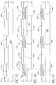
- FIG. 2Ais a cross-sectional view illustrating a resistance variable material cell 200 according to one embodiment of the invention.
- the resistance variable material cell 200can be fabricated on top of a variety of structures including semiconductors and insulators.
- the resistance variable material cell 200includes a lower electrode 202 .
- the lower electrode 202can be formed from a variety of materials, such as tungsten (W), tungsten nitride (WN), and polysilicon.
- a layer of silver-rich silver selenide (Ag 2+x Se) 206forms an active layer of a body of the resistance variable material cell 200 .
- the layer of silver-rich silver selenide (Ag 2+x Se) 206is disposed between the lower electrode 202 and an upper electrode 210 .
- the illustrated resistance variable material cell 200also includes a layer of chalcogenide glass, which can be disposed on either side of the layer of silver-rich silver selenide (Ag 2+x Se) 206 .
- the layer of chalcogenide glasscan be disposed between the layer of silver-rich silver selenide (Ag 2+x Se) 206 and the lower electrode 202 as shown by a lower layer of chalcogenide glass 204 .
- the layer of chalcogenide glasscan alternatively be disposed between layer of silver-rich silver selenide (Ag 2+x Se) 206 and the upper electrode 210 as shown by an upper layer of chalcogenide glass 207 .
- the chalcogenide glasscan correspond to a variety of chalcogenide glasses and can include, for example, germanium selenide (Ge X Se 1 ⁇ x ).
- the layer of silver rich silver selenide (Ag 2+x Se) 206is between about 100 ⁇ and about 1000 ⁇ thick. More preferably, the layer of silver rich silver selenide (Ag 2+x Se) 206 is between about 300 ⁇ and about 470 ⁇ thick.
- the upper electrode 210can be formed from a variety of materials, such as silver (Ag), titanium (Ti), tungsten (W), tungsten nitride (WN), and the like.
- a conductive pathwayis formed or is disrupted in the resistance variable material cell 200 .
- the conductive pathway(or lack thereof) can persist after the removal of the applied electric potential. This property can permit a resistance variable material cell to retain information in a nonvolatile manner.
- An insulator 208insulates the body of the resistance variable material cell 200 from other memory cells and also prevents the undesired diffusion of active material.
- the insulator 208can be formed from a variety of materials such as silicon nitride (Si 3 N 4 ). Of course, the insulator 208 can be formed in multiple steps and can include multiple structures.
- FIG. 2Bis a cross-sectional view illustrating a resistance variable material cell 250 with a conductive plug according to one embodiment of the invention.
- the illustrated resistance variable material cell 250includes a plug 214 of conductive material, such as tungsten (W) formed in an opening or via defined in the insulator 208 .
- the plug 214is disposed between the lower electrode 202 and the upper electrode 210 .
- the addition of the plug 214can help to prevent the inadvertent or unintended shorting of the lower electrode 202 and the upper electrode 210 .
- a lower layer of chalcogenide glass 205is disposed between the plug 214 and the layer of silver-rich silver selenide (Ag 2+x Se) 206
- an upper layer of chalcogenide glass 207is disposed between the layer of silver-rich silver selenide (Ag 2+x Se) 206 and the upper electrode 210 .
- the resistance variable material cell 250can include those embodiments with only one of the lower layer of chalcogenide glass 205 or the upper layer of chalcogenide glass 207 , or embodiments with both as illustrated in FIG. 2B .
- the plug 214is disposed between the layer of silver-rich silver selenide (Ag 2+x Se) 206 and the lower electrode 202 . It will be understood by the skilled practitioner that the relative location of the plug 214 and the layer of silver-rich silver selenide (Ag 2+x Se) 206 can be interchanged, such that the plug 214 can be disposed between the layer of silver-rich silver selenide (Ag 2+x Se) 206 and the upper electrode 210 .
- a layer of silver-permeable materialsuch as a layer of germanium selenide, can also be disposed between the layer of silver-rich silver selenide (Ag 2+x Se) 206 and the lower electrode 202 or the upper electrode 210 .
- the plug 214should be formed from a conductive material, such as tungsten (W).
- the illustrated plug 214provides electrical continuity between the lower electrode 202 and the layer of silver-rich silver selenide (Ag 2+x Se) 206 or between the lower electrode 202 and the lower layer of chalcogenide glass 205 , where present.
- the plug 214is formed such that the plug 214 is relatively level with the insulator 208 in which an opening or via for the plug 214 is formed.
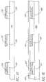
- FIGS. 3A–Eare cross-sectional views illustrating an array of resistance variable material cells in various stages of construction. It will be understood by one of ordinary skill in the art that the number of cells in an array can vary in a very broad range. In FIGS. 3A–E , three cells are shown for the purposes of illustration.
- FIG. 3Aillustrates a portion of a substrate assembly with a substrate 302 , a first lower electrode 304 , a second lower electrode 306 , and a third lower electrode 308 .
- the substratecan correspond to a variety of substrates, such as an insulating substrate, a semiconductor substrate, or an insulating layer on a semiconductor substrate.
- the memory cellswill be described in the context of silver selenide as the metal-doped chalcogenide.
- a layer of silver selenide 310is formed above the substrate 302 , the first lower electrode 304 , the second lower electrode 306 , and the third lower electrode 308 .
- the layer of silver selenide 310can be formed from stoichiometric silver selenide (Ag 2 Se) or from slightly silver-rich or silver-poor silver selenide.
- FIG. 3Billustrates the portion of the substrate assembly with a patterned mask.
- the patterned maskis formed on top of the layer of silver selenide 310 and is used to permit the selective implantation of oxygen. It will be understood that the layer of silver selenide 310 can be implanted with oxygen without a patterned mask.
- the illustrated patterned maskincludes a first portion of photoresist 312 and a second portion of photoresist 314 .
- the patterned maskis formed from a layer of photoresist material that is patterned using photolithography.
- the patterned maskis form from a hard mask, such as a mask of silicon nitride. Openings 316 are defined in the pattern mask to selectively provide access to the layer of silver selenide 310 such that oxygen can correspondingly be selectively implanted in the layer of silver selenide 310 .
- a first region 318 , a second region 320 , and a third region 322are implanted with oxygen.
- the oxygen implanter toolcan be configured to implant oxygen to a variety of depths. In one embodiment, the depth or range of implantation corresponds to approximately 100 ( ⁇ ).
- the pattern maskis removed, and the substrate assembly is annealed.
- Annealingremoves selenium oxide from the implanted regions of the layer of silver selenide illustrated by the first region 318 , the second region 320 and the third region 322 , thereby leaving silver-rich regions in the layer of silver selenide.
- These silver-rich regionsare illustrated by a first silver rich-region 328 , a second silver-rich region 330 , and a third silver-rich region 332 .
- patterning, implanting, and annealing of the silver selenide layercan be repeated multiple times to increase the amount of silver-richness in the silver selenide layer.
- FIG. 3Dillustrates the first silver-rich region 328 , the second silver-rich region 330 , and the third silver-rich region 332 that have been patterned into cells from the layer of silver selenide.
- a variety of techniquescan be used to pattern cells including, for example, wet etching, reactive ion etching (RIE) and ion beam etching (IBE) techniques. It will be understood by one of ordinary skill in the art that such patterning techniques can also include additional mask patterning steps.
- RIEreactive ion etching
- IBEion beam etching
- a layer of an insulatorcan be formed to fill the space between the cells.
- the layer of insulatorcan be made from a variety of materials, such as silicon nitride or polyimide.
- a chemical-mechanical polish (CMP)can smooth out the top of the layer of the insulator.
- a portion of the insulatorcan also be formed between the cell and the upper electrode, and the vias and plugs can be landed on the layer of silver-rich silver selenide to provide electrical continuity to the upper electrode.
- FIG. 3Eillustrates an upper electrode 334 formed above cells patterned from the first silver-rich region 328 , the second silver-rich region 330 , and the third silver-rich region 332 .
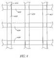
- FIG. 4is a schematic top-down view that illustrates an array of resistance variable material cells in a cross-point configuration. It will be understood that a resistance variable material cell can also be isolated and coupled to transistors for read and write operations.
- the portion of the array shown in FIG. 4includes 9 resistance variable material cells, but it will be understood by one of ordinary skill in the art that the number of cells in an array can vary in a very broad range.
- the arrayincludes lower electrodes, as illustrated by a first lower electrode 402 , a second lower electrode 404 , and a third lower electrode 406 .
- the arrayalso includes upper electrodes, as illustrated by a first upper electrode 408 , a second upper electrode 410 , and a third upper electrode 412 . In the illustrated cross-point configuration, the lower electrodes and the upper electrodes are arranged in an approximately orthogonal manner, but it will be understood that other configurations are possible.
- Memory cellslie between the lower electrodes and the upper electrodes approximately where the electrodes cross.
- a first resistance variable material cell 414is disposed between the first lower electrode 402 and the first upper electrode 408 .
- the contents of the first resistance variable material cell 414can be accessed (for reading or writing) by activating the first lower electrode 402 and the first upper electrode 408 .
- Informationcan be stored in a cell by forming or by disrupting conductive pathways, which varies the resistance of the cell. When an electric potential is applied between the upper electrode and the lower electrode, an electric field is generated in the layer of resistance variable material.
- a conductive pathwaygrows from the electrode configured as the cathode, i.e., the electrode with the more negative electric potential, to the electrode configured as the anode, i.e., the electrode with the more positive electric potential.
- Informationcan be read or retrieved from the cell by sensing the resistance of the cell.
Landscapes
- Engineering & Computer Science (AREA)
- Manufacturing & Machinery (AREA)
- Semiconductor Memories (AREA)
Abstract
Description
This application is a divisional of application Ser. No. 10/231,779 filed Aug. 29, 2002 now U.S. Pat. No. 6,867,114, which is incorporated herein by reference.
1. Field of the Invention
The invention generally relates to memory technology. In particular, the invention relates to memory devices with a metal-rich metal chalcogenide, such as silver-rich silver selenide.
2. Description of the Related Art
Computers and other digital systems use memory to store programs and data. A common form of memory is random access memory (RAM). Many memory devices, such as dynamic random access memory (DRAM) devices and static random access memory (SRAM) devices are volatile memories. A volatile memory loses its data when power is removed. In addition, certain volatile memories such as DRAM devices require periodic refresh cycles to retain their data even when power is continuously supplied.
In contrast to the potential loss of data encountered in volatile memory devices, nonvolatile memory devices retain data when power is removed. Examples of nonvolatile memory devices include read only memory (ROM), programmable read only memory (PROM), erasable programmable read only memory (EPROM), electrically erasable programmable read only memory (EEPROM), Flash ROM, and the like.
One type of memory device is known as a programmable conductor memory cell or a programmable metallization cell (PMC). See U.S. Pat. Nos. 5,761,115; 5,896,312; 5,914,893; and 6,084,796 to Kozicki, et al., entitled “Programmable metallization cell structure and method of making same,” the disclosures of which are hereby incorporated by reference in their entirety herein. Also see PCT publications WO 00/48196 and WO 02/21542 for additional information. Another term used to describe this cell is a resistance variable material cell. These memory cells can be nonvolatile. A programmable conductor random access memory (PCRAM) includes an array of programmable metallization cells or resistance variable material cells. Additional applications for a programmable metallization cell include use as a programmable resistance and a programmable capacitance.
Information can be stored in a resistance variable material cell by forming or by disrupting conductive pathways, which varies the resistance of the cell. In response to an applied electric field, which can be generated by an electric potential applied between electrodes, a conductive pathway grows from an electrode configured as the cathode, i.e., the electrode with the more negative electric potential, to an electrode configured as the anode, i.e., the electrode with the more positive electric potential. Information can be read or retrieved from the cell by sensing the resistance of the cell.
Conventional processes include techniques that diffuse silver (Ag) through a silver-permeable material, such as a chalcogenide glass. One example of a chalcogenide glass is germanium selenide (GexSe1−x). For example, one conventional process for producing a PMC applies silver (Ag) photodoping to a chalcogenide glass, such as germanium selenide, e.g., Ge3Se7. It is relatively difficult to diffuse silver uniformly across a wafer using conventional techniques. For example, in one conventional process, the doping of the silver varies across the wafer by about 5 to 10%, which can reduce production yield.
Silver-rich silver selenide is relatively difficult to produce using direct deposition techniques. For example, when silver (Ag) is directly deposited on silver selenide (Ag2−δSe), where 0≦δ≦1, in an attempt to create silver-rich silver selenide (Ag2+xSe), the silver (Ag) may agglomerate on the silver selenide and create a rough surface. Similar results may occur when attempting to deposit silver selenide (Ag2Se) directly on silver (Ag).
What is needed is a process to enrich a material, including non-transparent materials, with a metal, such as silver (Ag), to fabricate materials such as silver-rich silver selenide (Ag2+xSe) or silver-rich silver telluride (Ag2+xTe). Such materials can be useful in cell bodies of memory devices.
The invention relates to the fabrication of a resistance variable material cell or programmable metallization cell (PMC). Advantageously, the processes described herein can form a layer of a metal-rich metal chalcogenide, such as silver-rich silver selenide (Ag2+xSe), without the use of photodoping techniques and without direct deposition of the metal. Further advantageously, the processes can dope a metal, such as silver, into materials that are not transparent. In addition, the processes can form materials such as silver-rich silver selenide (Ag2+xSe) with relatively high uniformity and with relatively precise control.
One process according to an embodiment of the invention forms silver-rich silver selenide (Ag2+xSe) for a cell body for a resistance variable material cell. The process includes forming a layer of silver selenide, implanting oxygen to form selenium oxide, and annealing to remove the selenium oxide, thereby forming the silver-rich silver selenide (Ag2+xSe). In one embodiment, regions of a wafer are selectively enriched with silver by patterning the oxygen implantation. One embodiment of the process repeatedly performs implanting of oxygen and annealing to increase an amount of silver in the silver-rich silver selenide.
These and other features of the invention will now be described with reference to the drawings summarized below. These drawings (not to scale) and the associated description are provided to illustrate preferred embodiments of the invention and are not intended to limit the scope of the invention.
Although this invention will be described in terms of certain preferred embodiments, other embodiments that are apparent to those of ordinary skill in the art, including embodiments that do not provide all of the benefits and features set forth herein, are also within the scope of this invention. For example, while illustrated in the context of particular materials, the skilled artisan will appreciate that the methods described herein are applicable to doping a variety of materials with tailored amounts of metal, for a variety of applications. Accordingly, the scope of the invention is defined only by reference to the appended claims.
One process according to an embodiment of the invention can form silver-rich silver chalcogenide for use in a resistance variable material cell. The silver-rich silver chalcogenide cells include at least one layer of a silver-rich silver chalcogenide and at least one layer of a chalcogenide glass, such as germanium selenide (GexSe1−x). The process can be automated such that it is under computer control. Advantageously, the process is capable of increasing the silver content of materials in a relatively uniform and well-controlled manner. For example, the process can form silver-rich silver selenide (Ag2+xSe), silver-rich silver telluride, and the like. The silver-rich regions can be formed in a pattern across a wafer. Cells in an array of cells can be patterned to remove non-enriched regions.
These silver-rich silver chalcogenide cells can be used to store memory states, programmed resistances, and the like. When an electric potential is applied between the first electrode and the second electrode, a conductive pathway is formed or is disrupted (depending upon the polarity of the potential) in a layer of silver-permeable material, such as germanium selenide (GexSe1−x), thereby varying the resistance of the cell. The formation of the conductive pathway lowers the resistance between the electrodes. The conductive pathway can persist after the removal of the applied electric potential. This property can permit some embodiments of a resistance variable material cell to retain information in a nonvolatile manner.
While the silver chalcogenide is illustrated primarily in the context of silver selenide, the skilled artisan will appreciate that the principles and advantages described herein are applicable to other silver chalcogenides. For example, other applicable silver chalcogenides can also include silver sulfide and silver telluride.
The process forms110 a lower electrode on the substrate assembly. The process can form110 the lower electrode by forming a conductive film, which can be formed from a variety of materials, such as tungsten (W), tungsten nitride (WN), polysilicon, and others. It will be understood by one of ordinary skill in the art that the lower electrode can also include a barrier layer.
The process can proceed to form115 a layer of chalcogenide glass, such as germanium selenide (GexSe1−x), on the lower electrode. The process can include forming the layer of chalcogenide glass below a layer of silver selenide, above the layer of silver selenide, or both. It will thus be understood that in some embodiments of the process, the forming115 of the layer of chalcogenide glass on the lower electrode is optional. Where the layer of chalcogenide glass is formed115 on the lower electrode, the layer of chalcogenide glass is preferably between about 50 angstroms (Å) to about 1000 (Å) thick. In one embodiment, the layer of chalcogenide glass is about 150 Å thick. An exemplary chalcogenide glass is Ge0.4Se0.6.
The process proceeds to form120 the layer of silver selenide. It will be understood that the layer of silver selenide can be formed on the lower electrode when the process does not form a layer of chalcogenide glass below the layer of silver selenide. When the process forms the layer of chalcogenide glass on the lower electrode, the layer of silver selenide can be formed on the layer of chalcogenide glass. Although the layer of silver selenide can be formed with stoichiometric silver selenide (Ag2Se), it will be understood that the silver selenide can also initially be slightly silver-rich or silver-poor, depending on the deposition process. A variety of techniques can be used to form the layer of silver selenide. Preferably, physical vapor deposition (PVD) techniques, such as evaporative deposition and sputtering, are used to form120 the layer of silver selenide. In addition, the process can form120 the layer of silver selenide as a single layer or in multiple layers. Although a variety of techniques are available for forming silver selenide, precise control over the composition is difficult with conventional techniques.
The process proceeds to implant130 oxygen. Implanting of oxygen converts at least some of the silver selenide to silver-rich silver selenide (Ag2+xSe) and to selenium oxide (SeO2). A simplified chemical equation (not balanced) is provided in Equation 1.
Ag2Se+O2→Ag2+xSe+SeO2 (Eq. 1)
Ag2Se+O2→Ag2+xSe+SeO2 (Eq. 1)
Ion implantation techniques are preferably used to implant the oxygen into the layer of silver selenide. Advantageously, ion implantation is a relatively well-controlled process, which correspondingly permits the amount of silver richness, x, in the silver-rich silver selenide (Ag2+xSe) to be relatively well controlled. For example, ion implantation techniques can implant oxygen with less than 1% variation across a layer of silver selenide on the surface of a wafer. By contrast, a variation in uniformity of around 5 to 10 percent across the surface of a wafer can be expected from techniques that directly deposit silver or photodope silver.
Preferably, oxygen is implanted at a relatively high dosage. The high dosage permits the amount of silver richness, x, to be correspondingly high. Preferably, x is in a range of about 0 to about 10%. More preferably, x is in a range of about 1% to about 3%. Preferably, the oxygen is implanted to a relatively shallow depth that is relatively close to the surface. In one embodiment, the oxygen implanter tool is configured to implant oxygen to a depth or range of about 100 (Å) with a setting of about 1 to about 3 kilo-electron volts (keV). In addition, implanting130 of oxygen and annealing140 of the substrate assembly can be repeated as described later in connection with anoptional decision block 150.
Implanting130 of oxygen can be selectively applied to the layer of silver selenide. A pattern mask, such as a mask of photoresist, can be formed over the layer of silver selenide to allow the ion implantation to implant oxygen to selected areas. The presence of the pattern mask blocks implantation of oxygen from selected areas. The pattern mask includes open windows that permit implantation of oxygen in other areas. In another embodiment, implanting130 of oxygen is applied to the layer of silver selenide without patterning.
The process proceeds to anneal140 the substrate assembly. Annealing140 removes the selenium oxide from the layer. Where implanting of oxygen has been carried out in a patterned manner, regions of silver selenide (Ag2Se) and silver-rich/silver selenide (Ag2+xSe) are left after annealing. Prior to annealing140 the substrate assembly, the pattern mask, if present, should be removed.
Annealing140 includes heating the substrate assembly in a chamber, which is maintained at a relatively low pressure. In one embodiment, the substrate assembly is heated such that a vapor pressure of selenium oxide (or more generally, the oxide of the element to be removed) is greater than the pressure maintained in an annealing chamber. Annealing140 can be performed at a broad range of pressures and temperatures. Annealing140 can be performed for a predetermined time using data collected from experimental results. Endpoint detection techniques, such as optical emission spectroscopy techniques, can also be used to determine when to stop annealing. In one embodiment, annealing140 is performed at a temperature between about 50 degrees centigrade (C) to about 130 degrees C. for a time period of about 30 minutes to about 3 hours. Preferably, annealing is performed at a temperature of about 90 degrees C.
The process proceeds to anoptional decision block 150, where the process determines whether to repeat implanting130 andannealing 140. Implanting130 and annealing140 can be repeated multiple times to increase the amount of silver richness, i.e., the value of x, in silver-rich silver selenide (Ag2+xSe). The number of times that implanting130 and annealing140 is repeated can be predetermined. A counter, which can be implemented in a computer memory, can track the number of iterations of implanting130 andannealing 140. If implanting130 and annealing140 are to be repeated, the process returns from theoptional decision block 150 to implanting130. Otherwise, the process proceeds topattern 160 cells. When implanting130 is repeated, the process can implant to the same depth or to different depths.
The process canpattern 160 cells in accordance with a variety of techniques. Patterning techniques that can be used include reactive ion etch (RIE) and ion beam etching (IBE) techniques. In one embodiment, a potassium iodide/iodide (KI/I2) solution is used with a pattern mask to selectively etch and thereby pattern cells. It will be understood by one of ordinary skill in the art that patterning160 of cells may require additional steps, such as mask patterning and etching in conjunction with the mask.
The process can then form165 a layer of chalcogenide glass on the patterned layer of silver selenide. As described earlier, the process can form the layer of chalcogenide glass below the layer of silver selenide, above the layer of silver selenide, or both. Thus, it will be understood that in some embodiments of the process, the process does not form the layer of chalcogenide glass on the layer of silver selenide.
The process then forms170 an upper electrode. The upper electrode can be formed from a variety of materials, such as silver (Ag), titanium (Ti), tungsten (W), tungsten nitride (WN), and the like. When the process forms165 the layer of chalcogenide glass on the patterned layer of silver selenide, the process can form170 the upper electrode on the layer of chalcogenide glass. When the process does not form165 the layer of chalcogenide glass, the process can form170 the upper electrode on the patterned layer of silver selenide. It will be understood by one of ordinary skill in the art that the upper electrode can also include barrier layers preferably formed from the same metal that dopes the film.
In another embodiment of the process, the process optionally forms a layer of insulating material between the lower electrode and the upper electrode. One embodiment of a resistance variable material cell or PCRAM cell with such an insulating layer is described in greater detail later in connection withFIG. 2B . The insulating layer can be formed on the lower electrode, or the insulating layer can be formed between the silver-rich silver selenide (Ag2+xSe) layer and the upper electrode. Advantageously, the insulating layer can prevent the unintended shorting of the lower and upper electrodes. The insulating layer can be formed from a variety of dielectrics including, for example, silicon nitride (Si3N4). The insulating layer includes vias, which can be filled with plugs of conductive material to provide electrical continuity between the lower electrode and the silver-rich silver selenide (Ag2+xSe) layer or between the upper electrode and the silver-rich silver selenide (Ag2+xSe) layer. An example of a suitable material for such a plug is tungsten (W).
A layer of silver-rich silver selenide (Ag2+xSe)206 forms an active layer of a body of the resistancevariable material cell 200. The layer of silver-rich silver selenide (Ag2+xSe)206 is disposed between thelower electrode 202 and anupper electrode 210. The illustrated resistancevariable material cell 200 also includes a layer of chalcogenide glass, which can be disposed on either side of the layer of silver-rich silver selenide (Ag2+xSe)206. For example, the layer of chalcogenide glass can be disposed between the layer of silver-rich silver selenide (Ag2+xSe)206 and thelower electrode 202 as shown by a lower layer ofchalcogenide glass 204. The layer of chalcogenide glass can alternatively be disposed between layer of silver-rich silver selenide (Ag2+xSe)206 and theupper electrode 210 as shown by an upper layer ofchalcogenide glass 207. It will be understood that the chalcogenide glass can correspond to a variety of chalcogenide glasses and can include, for example, germanium selenide (GeXSe1−x). Preferably, the layer of silver rich silver selenide (Ag2+xSe)206 is between about 100 Å and about 1000 Å thick. More preferably, the layer of silver rich silver selenide (Ag2+xSe)206 is between about 300 Å and about 470 Å thick. Theupper electrode 210 can be formed from a variety of materials, such as silver (Ag), titanium (Ti), tungsten (W), tungsten nitride (WN), and the like.
In response to a difference in electric potential applied between the lower electrode and the upper electrode, a conductive pathway is formed or is disrupted in the resistancevariable material cell 200. The conductive pathway (or lack thereof) can persist after the removal of the applied electric potential. This property can permit a resistance variable material cell to retain information in a nonvolatile manner.
Aninsulator 208 insulates the body of the resistancevariable material cell 200 from other memory cells and also prevents the undesired diffusion of active material. Theinsulator 208 can be formed from a variety of materials such as silicon nitride (Si3N4). Of course, theinsulator 208 can be formed in multiple steps and can include multiple structures.
In the illustrated embodiment of the resistancevariable material cell 250, a lower layer ofchalcogenide glass 205 is disposed between theplug 214 and the layer of silver-rich silver selenide (Ag2+xSe)206, and an upper layer ofchalcogenide glass 207 is disposed between the layer of silver-rich silver selenide (Ag2+xSe)206 and theupper electrode 210. It will be understood that the resistancevariable material cell 250 can include those embodiments with only one of the lower layer ofchalcogenide glass 205 or the upper layer ofchalcogenide glass 207, or embodiments with both as illustrated inFIG. 2B .
In the illustrated embodiment of the resistancevariable material cell 250, theplug 214 is disposed between the layer of silver-rich silver selenide (Ag2+xSe)206 and thelower electrode 202. It will be understood by the skilled practitioner that the relative location of theplug 214 and the layer of silver-rich silver selenide (Ag2+xSe)206 can be interchanged, such that theplug 214 can be disposed between the layer of silver-rich silver selenide (Ag2+xSe)206 and theupper electrode 210. It will also be understood that a layer of silver-permeable material, such as a layer of germanium selenide, can also be disposed between the layer of silver-rich silver selenide (Ag2+xSe)206 and thelower electrode 202 or theupper electrode 210.
Theplug 214 should be formed from a conductive material, such as tungsten (W). The illustratedplug 214 provides electrical continuity between thelower electrode 202 and the layer of silver-rich silver selenide (Ag2+xSe)206 or between thelower electrode 202 and the lower layer ofchalcogenide glass 205, where present. Preferably, theplug 214 is formed such that theplug 214 is relatively level with theinsulator 208 in which an opening or via for theplug 214 is formed.
The cells of resistance variable materials are preferably arranged in an array of cells. The array advantageously permits a relatively large number of cells, and thereby a relatively large memory space, to be fabricated contemporaneously.FIGS. 3A–E are cross-sectional views illustrating an array of resistance variable material cells in various stages of construction. It will be understood by one of ordinary skill in the art that the number of cells in an array can vary in a very broad range. InFIGS. 3A–E , three cells are shown for the purposes of illustration.
A layer ofsilver selenide 310 is formed above thesubstrate 302, the firstlower electrode 304, the secondlower electrode 306, and the thirdlower electrode 308. The layer ofsilver selenide 310 can be formed from stoichiometric silver selenide (Ag2Se) or from slightly silver-rich or silver-poor silver selenide.
As illustrated inFIG. 3B , afirst region 318, asecond region 320, and athird region 322 are implanted with oxygen. The oxygen implanter tool can be configured to implant oxygen to a variety of depths. In one embodiment, the depth or range of implantation corresponds to approximately 100 (Å).
InFIG. 3C , the pattern mask is removed, and the substrate assembly is annealed. Annealing removes selenium oxide from the implanted regions of the layer of silver selenide illustrated by thefirst region 318, thesecond region 320 and thethird region 322, thereby leaving silver-rich regions in the layer of silver selenide. These silver-rich regions are illustrated by a first silver rich-region 328, a second silver-rich region 330, and a third silver-rich region 332. As described earlier in connection withFIG. 1 , patterning, implanting, and annealing of the silver selenide layer can be repeated multiple times to increase the amount of silver-richness in the silver selenide layer.
In addition, it will be understood that in-between patterning of cells and forming of upper electrodes, a layer of an insulator can be formed to fill the space between the cells. The layer of insulator can be made from a variety of materials, such as silicon nitride or polyimide. A chemical-mechanical polish (CMP) can smooth out the top of the layer of the insulator. A portion of the insulator can also be formed between the cell and the upper electrode, and the vias and plugs can be landed on the layer of silver-rich silver selenide to provide electrical continuity to the upper electrode.
After patterning of the cells, upper electrodes are formed on top of the cells patterned from the silver rich-regions. For example,FIG. 3E illustrates anupper electrode 334 formed above cells patterned from the first silver-rich region 328, the second silver-rich region 330, and the third silver-rich region 332.
Memory cells lie between the lower electrodes and the upper electrodes approximately where the electrodes cross. For example, a first resistancevariable material cell 414 is disposed between the firstlower electrode 402 and the firstupper electrode 408. The contents of the first resistancevariable material cell 414 can be accessed (for reading or writing) by activating the firstlower electrode 402 and the firstupper electrode 408. Information can be stored in a cell by forming or by disrupting conductive pathways, which varies the resistance of the cell. When an electric potential is applied between the upper electrode and the lower electrode, an electric field is generated in the layer of resistance variable material. In response to the electric field, a conductive pathway grows from the electrode configured as the cathode, i.e., the electrode with the more negative electric potential, to the electrode configured as the anode, i.e., the electrode with the more positive electric potential. Information can be read or retrieved from the cell by sensing the resistance of the cell.
Various embodiments of the invention have been described above. Although this invention has been described with reference to these specific embodiments, the descriptions are intended to be illustrative of the invention and are not intended to be limiting. Various modifications and applications may occur to those skilled in the art without departing from the true spirit and scope of the invention as defined in the appended claims.
Claims (9)
1. A method of forming memory cells in a programmable conductor random access memory (PCRAM) comprising:
(a) forming a plurality of electrodes;
(b) forming a layer of chalcogenide glass;
(c) forming a layer of silver selenide adjacent to the layer of chalcogenide glass;
(d) forming a mask pattern over the layer of silver selenide;
(e) implanting unmasked portions of the layer of silver selenide with oxygen;
(f) removing the mask pattern;
(g) annealing the layer of implanted silver selenide such that the layer is essentially free of selenium oxide thereby forming silver-rich regions of silver selenide; and
(h) patterning to define cells, where patterning selectively removes unenriched regions of silver selenide.
2. The method as defined inclaim 1 , further comprising repeating (d) to (g) to further increase an amount of silver in the silver-rich regions of silver selenide.
3. The process as defined inclaim 1 , further comprising forming electrodes in a cross-point configuration.
4. The process as defined inclaim 1 , wherein the layer of chalcogenide glass is formed before forming the layer of silver selenide.
5. The process as defined inclaim 1 , wherein the layer of chalcogenide glass is formed after forming, implanting, annealing, and patterning the layer of silver selenide.
6. A process to increase a ratio of silver to a chalcogenide material in a composition of silver chalcogenide, comprising:
providing silver chalcogenide; and
removing a selected amount of chalcogenide from the silver chalcogenide by implanting oxygen into the silver chalcogenide and annealing the oxygen-implanted silver chalcogenide.
7. The process as defined inclaim 6 , further comprising repeating implanting and annealing for a predetermined number of times to further increase the ratio of silver to chalcogenide.
8. The process as defined inclaim 6 , wherein the silver chalcogenide is selected from the group consisting of silver selenide, silver telluride, and silver sulfide.
9. The process as defined inclaim 6 , wherein the silver chalcogenide is silver selenide.
Priority Applications (2)
| Application Number | Priority Date | Filing Date | Title |
|---|---|---|---|
| US10/769,787US7056762B2 (en) | 2002-08-29 | 2004-02-03 | Methods to form a memory cell with metal-rich metal chalcogenide |
| US11/258,921US7294527B2 (en) | 2002-08-29 | 2005-10-27 | Method of forming a memory cell |
Applications Claiming Priority (2)
| Application Number | Priority Date | Filing Date | Title |
|---|---|---|---|
| US10/231,779US6867114B2 (en) | 2002-08-29 | 2002-08-29 | Methods to form a memory cell with metal-rich metal chalcogenide |
| US10/769,787US7056762B2 (en) | 2002-08-29 | 2004-02-03 | Methods to form a memory cell with metal-rich metal chalcogenide |
Related Parent Applications (1)
| Application Number | Title | Priority Date | Filing Date |
|---|---|---|---|
| US10/231,779DivisionUS6867114B2 (en) | 2002-08-29 | 2002-08-29 | Methods to form a memory cell with metal-rich metal chalcogenide |
Related Child Applications (1)
| Application Number | Title | Priority Date | Filing Date |
|---|---|---|---|
| US11/258,921Continuation-In-PartUS7294527B2 (en) | 2002-08-29 | 2005-10-27 | Method of forming a memory cell |
Publications (2)
| Publication Number | Publication Date |
|---|---|
| US20040157417A1 US20040157417A1 (en) | 2004-08-12 |
| US7056762B2true US7056762B2 (en) | 2006-06-06 |
Family
ID=31976812
Family Applications (2)
| Application Number | Title | Priority Date | Filing Date |
|---|---|---|---|
| US10/231,779Expired - LifetimeUS6867114B2 (en) | 2002-08-29 | 2002-08-29 | Methods to form a memory cell with metal-rich metal chalcogenide |
| US10/769,787Expired - Fee RelatedUS7056762B2 (en) | 2002-08-29 | 2004-02-03 | Methods to form a memory cell with metal-rich metal chalcogenide |
Family Applications Before (1)
| Application Number | Title | Priority Date | Filing Date |
|---|---|---|---|
| US10/231,779Expired - LifetimeUS6867114B2 (en) | 2002-08-29 | 2002-08-29 | Methods to form a memory cell with metal-rich metal chalcogenide |
Country Status (1)
| Country | Link |
|---|---|
| US (2) | US6867114B2 (en) |
Cited By (10)
| Publication number | Priority date | Publication date | Assignee | Title |
|---|---|---|---|---|
| US20060226410A1 (en)* | 2005-04-11 | 2006-10-12 | Wicker Guy C | Heating phase change material |
| US20080121859A1 (en)* | 2006-10-19 | 2008-05-29 | Boise State University | Forced ion migration for chalcogenide phase change memory device |
| US20090231910A1 (en)* | 2008-03-11 | 2009-09-17 | Micron Technology, Inc. | Non-volatile memory with resistive access component |
| US20100027324A1 (en)* | 2008-08-01 | 2010-02-04 | Boise State University | Variable integrated analog resistor |
| US20100032732A1 (en)* | 2008-08-06 | 2010-02-11 | International Business Machines Corporation | Electrical antifuse having a multi-thickness dielectric layer |
| US20100072448A1 (en)* | 2008-09-19 | 2010-03-25 | Seagate Technology Llc | Planar programmable metallization memory cells |
| US20110079709A1 (en)* | 2009-10-07 | 2011-04-07 | Campbell Kristy A | Wide band sensor |
| US8284590B2 (en) | 2010-05-06 | 2012-10-09 | Boise State University | Integratable programmable capacitive device |
| US8467236B2 (en) | 2008-08-01 | 2013-06-18 | Boise State University | Continuously variable resistor |
| US10388371B2 (en) | 2015-01-26 | 2019-08-20 | Agency For Science, Technology And Research | Memory cell selector and method of operating memory cell |
Families Citing this family (26)
| Publication number | Priority date | Publication date | Assignee | Title |
|---|---|---|---|---|
| DE102004014965B4 (en)* | 2004-03-26 | 2007-12-27 | Qimonda Ag | Method for producing a nonvolatile memory cell |
| US7224598B2 (en)* | 2004-09-02 | 2007-05-29 | Hewlett-Packard Development Company, L.P. | Programming of programmable resistive memory devices |
| DE102004052645A1 (en)* | 2004-10-29 | 2006-05-04 | Infineon Technologies Ag | Non-volatile (sic) resistive storage cell with solid electrolyte matrix between first and second electrode as active layer useful in semiconductor technology has elements from groups IVb and Vb and transition metals in active layer |
| US7138290B2 (en)* | 2004-12-03 | 2006-11-21 | Micron Technology, Inc. | Methods of depositing silver onto a metal selenide-comprising surface and methods of depositing silver onto a selenium-comprising surface |
| FR2880177B1 (en)* | 2004-12-23 | 2007-05-18 | Commissariat Energie Atomique | MEMORY PMC HAVING IMPROVED RETENTION TIME AND WRITING SPEED |
| US7709289B2 (en)* | 2005-04-22 | 2010-05-04 | Micron Technology, Inc. | Memory elements having patterned electrodes and method of forming the same |
| US7427770B2 (en)* | 2005-04-22 | 2008-09-23 | Micron Technology, Inc. | Memory array for increased bit density |
| US20070210297A1 (en)* | 2006-03-13 | 2007-09-13 | Ralf Symanczyk | Electrical structure with a solid state electrolyte layer, memory with a memory cell and method for fabricating the electrical structure |
| US7615771B2 (en)* | 2006-04-27 | 2009-11-10 | Hitachi Global Storage Technologies Netherlands, B.V. | Memory array having memory cells formed from metallic material |
| US7560723B2 (en)* | 2006-08-29 | 2009-07-14 | Micron Technology, Inc. | Enhanced memory density resistance variable memory cells, arrays, devices and systems including the same, and methods of fabrication |
| US7658773B2 (en)* | 2006-09-29 | 2010-02-09 | Qimonda Ag | Method for fabricating a solid electrolyte memory device and solid electrolyte memory device |
| FR2922368A1 (en)* | 2007-10-16 | 2009-04-17 | Commissariat Energie Atomique | METHOD FOR MANUFACTURING A CBRAM MEMORY HAVING IMPROVED RELIABILITY |
| US8097902B2 (en)* | 2008-07-10 | 2012-01-17 | Seagate Technology Llc | Programmable metallization memory cells via selective channel forming |
| MX2012005951A (en) | 2009-11-24 | 2012-10-01 | Opko Diagnostics Llc | Fluid mixing and delivery in microfluidic systems. |
| CA2795211C (en) | 2010-04-16 | 2018-11-06 | Opko Diagnostics, Llc | Feedback control in microfluidic systems |
| KR101781621B1 (en) | 2010-12-14 | 2017-09-26 | 삼성전자주식회사 | Fabricating method of Resistance Changeable Memory device |
| US8962460B2 (en) | 2011-04-26 | 2015-02-24 | Micron Technology, Inc. | Methods of selectively forming metal-doped chalcogenide materials, methods of selectively doping chalcogenide materials, and methods of forming semiconductor device structures including same |
| JP5966289B2 (en)* | 2011-09-16 | 2016-08-10 | 富士通株式会社 | Semiconductor substrate manufacturing method and semiconductor device manufacturing method |
| US8956939B2 (en) | 2013-04-29 | 2015-02-17 | Asm Ip Holding B.V. | Method of making a resistive random access memory device |
| JP2014216647A (en) | 2013-04-29 | 2014-11-17 | エーエスエムアイピー ホールディング ビー.ブイ. | Method for manufacturing resistive random access memory having metal-doped resistive switching layer |
| US9472757B2 (en) | 2013-07-19 | 2016-10-18 | Asm Ip Holding B.V. | Method of making a resistive random access memory device |
| US9520562B2 (en) | 2013-07-19 | 2016-12-13 | Asm Ip Holding B.V. | Method of making a resistive random access memory |
| TWI627301B (en)* | 2017-02-17 | 2018-06-21 | 國立清華大學 | Method for preparing vertical heterojunction of metal chalcogenide |
| US11316484B2 (en)* | 2017-05-25 | 2022-04-26 | Boise State University | Optically gated transistor selector for variable resistive memory device |
| US10700226B2 (en)* | 2017-05-25 | 2020-06-30 | Boise State University | Optically activated transistor, switch, and photodiode |
| US10930844B2 (en)* | 2018-10-11 | 2021-02-23 | International Business Machines Corporation | Three-terminal oxygen intercalation neuromorphic devices |
Citations (184)
| Publication number | Priority date | Publication date | Assignee | Title |
|---|---|---|---|---|
| US3271591A (en) | 1963-09-20 | 1966-09-06 | Energy Conversion Devices Inc | Symmetrical current controlling device |
| US3622319A (en) | 1966-10-20 | 1971-11-23 | Western Electric Co | Nonreflecting photomasks and methods of making same |
| US3743847A (en) | 1971-06-01 | 1973-07-03 | Motorola Inc | Amorphous silicon film as a uv filter |
| US3961314A (en) | 1974-03-05 | 1976-06-01 | Energy Conversion Devices, Inc. | Structure and method for producing an image |
| US3966317A (en) | 1974-04-08 | 1976-06-29 | Energy Conversion Devices, Inc. | Dry process production of archival microform records from hard copy |
| US3983542A (en) | 1970-08-13 | 1976-09-28 | Energy Conversion Devices, Inc. | Method and apparatus for recording information |
| US4177474A (en) | 1977-05-18 | 1979-12-04 | Energy Conversion Devices, Inc. | High temperature amorphous semiconductor member and method of making the same |
| US4267261A (en) | 1971-07-15 | 1981-05-12 | Energy Conversion Devices, Inc. | Method for full format imaging |
| US4269935A (en) | 1979-07-13 | 1981-05-26 | Ionomet Company, Inc. | Process of doping silver image in chalcogenide layer |
| JPS56126916A (en) | 1980-03-10 | 1981-10-05 | Nippon Telegr & Teleph Corp <Ntt> | Manufacture of semiconductor device |
| US4312938A (en) | 1979-07-06 | 1982-01-26 | Drexler Technology Corporation | Method for making a broadband reflective laser recording and data storage medium with absorptive underlayer |
| US4316946A (en) | 1979-12-03 | 1982-02-23 | Ionomet Company, Inc. | Surface sensitized chalcogenide product and process for making and using the same |
| US4320191A (en) | 1978-11-07 | 1982-03-16 | Nippon Telegraph & Telephone Public Corporation | Pattern-forming process |
| US4405710A (en) | 1981-06-22 | 1983-09-20 | Cornell Research Foundation, Inc. | Ion beam exposure of (g-Gex -Se1-x) inorganic resists |
| US4419421A (en) | 1979-01-15 | 1983-12-06 | Max-Planck-Gesellschaft Zur Forderung Der Wissenschaften E.V. | Ion conductor material |
| US4499557A (en) | 1980-10-28 | 1985-02-12 | Energy Conversion Devices, Inc. | Programmable cell for use in programmable electronic arrays |
| US4597162A (en) | 1983-01-18 | 1986-07-01 | Energy Conversion Devices, Inc. | Method for making, parallel preprogramming or field programming of electronic matrix arrays |
| US4608296A (en) | 1983-12-06 | 1986-08-26 | Energy Conversion Devices, Inc. | Superconducting films and devices exhibiting AC to DC conversion |
| US4637895A (en) | 1985-04-01 | 1987-01-20 | Energy Conversion Devices, Inc. | Gas mixtures for the vapor deposition of semiconductor material |
| US4646266A (en) | 1984-09-28 | 1987-02-24 | Energy Conversion Devices, Inc. | Programmable semiconductor structures and methods for using the same |
| US4664939A (en) | 1985-04-01 | 1987-05-12 | Energy Conversion Devices, Inc. | Vertical semiconductor processor |
| US4668968A (en) | 1984-05-14 | 1987-05-26 | Energy Conversion Devices, Inc. | Integrated circuit compatible thin film field effect transistor and method of making same |
| US4670763A (en) | 1984-05-14 | 1987-06-02 | Energy Conversion Devices, Inc. | Thin film field effect transistor |
| US4671618A (en) | 1986-05-22 | 1987-06-09 | Wu Bao Gang | Liquid crystalline-plastic material having submillisecond switch times and extended memory |
| US4673957A (en) | 1984-05-14 | 1987-06-16 | Energy Conversion Devices, Inc. | Integrated circuit compatible thin film field effect transistor and method of making same |
| US4678679A (en) | 1984-06-25 | 1987-07-07 | Energy Conversion Devices, Inc. | Continuous deposition of activated process gases |
| US4710899A (en) | 1985-06-10 | 1987-12-01 | Energy Conversion Devices, Inc. | Data storage medium incorporating a transition metal for increased switching speed |
| US4728406A (en) | 1986-08-18 | 1988-03-01 | Energy Conversion Devices, Inc. | Method for plasma - coating a semiconductor body |
| US4737379A (en) | 1982-09-24 | 1988-04-12 | Energy Conversion Devices, Inc. | Plasma deposited coatings, and low temperature plasma method of making same |
| US4766471A (en) | 1986-01-23 | 1988-08-23 | Energy Conversion Devices, Inc. | Thin film electro-optical devices |
| US4769338A (en) | 1984-05-14 | 1988-09-06 | Energy Conversion Devices, Inc. | Thin film field effect transistor and method of making same |
| US4775425A (en) | 1987-07-27 | 1988-10-04 | Energy Conversion Devices, Inc. | P and n-type microcrystalline semiconductor alloy material including band gap widening elements, devices utilizing same |
| US4788594A (en) | 1986-10-15 | 1988-11-29 | Energy Conversion Devices, Inc. | Solid state electronic camera including thin film matrix of photosensors |
| US4795657A (en) | 1984-04-13 | 1989-01-03 | Energy Conversion Devices, Inc. | Method of fabricating a programmable array |
| US4800526A (en) | 1987-05-08 | 1989-01-24 | Gaf Corporation | Memory element for information storage and retrieval system and associated process |
| US4809044A (en) | 1986-08-22 | 1989-02-28 | Energy Conversion Devices, Inc. | Thin film overvoltage protection devices |
| US4818717A (en) | 1986-06-27 | 1989-04-04 | Energy Conversion Devices, Inc. | Method for making electronic matrix arrays |
| US4843443A (en) | 1984-05-14 | 1989-06-27 | Energy Conversion Devices, Inc. | Thin film field effect transistor and method of making same |
| US4845533A (en) | 1986-08-22 | 1989-07-04 | Energy Conversion Devices, Inc. | Thin film electrical devices with amorphous carbon electrodes and method of making same |
| US4847674A (en) | 1987-03-10 | 1989-07-11 | Advanced Micro Devices, Inc. | High speed interconnect system with refractory non-dogbone contacts and an active electromigration suppression mechanism |
| US4853785A (en) | 1986-10-15 | 1989-08-01 | Energy Conversion Devices, Inc. | Electronic camera including electronic signal storage cartridge |
| US4891330A (en) | 1987-07-27 | 1990-01-02 | Energy Conversion Devices, Inc. | Method of fabricating n-type and p-type microcrystalline semiconductor alloy material including band gap widening elements |
| US5128099A (en) | 1991-02-15 | 1992-07-07 | Energy Conversion Devices, Inc. | Congruent state changeable optical memory material and device |
| US5159661A (en) | 1990-10-05 | 1992-10-27 | Energy Conversion Devices, Inc. | Vertically interconnected parallel distributed processor |
| US5166758A (en) | 1991-01-18 | 1992-11-24 | Energy Conversion Devices, Inc. | Electrically erasable phase change memory |
| US5177567A (en) | 1991-07-19 | 1993-01-05 | Energy Conversion Devices, Inc. | Thin-film structure for chalcogenide electrical switching devices and process therefor |
| US5219788A (en) | 1991-02-25 | 1993-06-15 | Ibm Corporation | Bilayer metallization cap for photolithography |
| US5238862A (en) | 1992-03-18 | 1993-08-24 | Micron Technology, Inc. | Method of forming a stacked capacitor with striated electrode |
| US5272359A (en) | 1988-04-07 | 1993-12-21 | California Institute Of Technology | Reversible non-volatile switch based on a TCNQ charge transfer complex |
| US5296716A (en) | 1991-01-18 | 1994-03-22 | Energy Conversion Devices, Inc. | Electrically erasable, directly overwritable, multibit single cell memory elements and arrays fabricated therefrom |
| US5314772A (en) | 1990-10-09 | 1994-05-24 | Arizona Board Of Regents | High resolution, multi-layer resist for microlithography and method therefor |
| US5315131A (en) | 1990-11-22 | 1994-05-24 | Matsushita Electric Industrial Co., Ltd. | Electrically reprogrammable nonvolatile memory device |
| US5335219A (en) | 1991-01-18 | 1994-08-02 | Ovshinsky Stanford R | Homogeneous composition of microcrystalline semiconductor material, semiconductor devices and directly overwritable memory elements fabricated therefrom, and arrays fabricated from the memory elements |
| US5341328A (en) | 1991-01-18 | 1994-08-23 | Energy Conversion Devices, Inc. | Electrically erasable memory elements having reduced switching current requirements and increased write/erase cycle life |
| US5350484A (en) | 1992-09-08 | 1994-09-27 | Intel Corporation | Method for the anisotropic etching of metal films in the fabrication of interconnects |
| US5359205A (en) | 1991-11-07 | 1994-10-25 | Energy Conversion Devices, Inc. | Electrically erasable memory elements characterized by reduced current and improved thermal stability |
| US5360981A (en) | 1989-05-11 | 1994-11-01 | British Telecommunications Public Limited Company | Amorphous silicon memory |
| US5406509A (en) | 1991-01-18 | 1995-04-11 | Energy Conversion Devices, Inc. | Electrically erasable, directly overwritable, multibit single cell memory elements and arrays fabricated therefrom |
| US5414271A (en) | 1991-01-18 | 1995-05-09 | Energy Conversion Devices, Inc. | Electrically erasable memory elements having improved set resistance stability |
| US5500532A (en) | 1994-08-18 | 1996-03-19 | Arizona Board Of Regents | Personal electronic dosimeter |
| US5512328A (en) | 1992-08-07 | 1996-04-30 | Hitachi, Ltd. | Method for forming a pattern and forming a thin film used in pattern formation |
| US5512773A (en) | 1993-12-23 | 1996-04-30 | U.S. Philips Corporation | Switching element with memory provided with Schottky tunnelling barrier |
| US5534712A (en) | 1991-01-18 | 1996-07-09 | Energy Conversion Devices, Inc. | Electrically erasable memory elements characterized by reduced current and improved thermal stability |
| US5534711A (en) | 1991-01-18 | 1996-07-09 | Energy Conversion Devices, Inc. | Electrically erasable, directly overwritable, multibit single cell memory elements and arrays fabricated therefrom |
| US5536947A (en) | 1991-01-18 | 1996-07-16 | Energy Conversion Devices, Inc. | Electrically erasable, directly overwritable, multibit single cell memory element and arrays fabricated therefrom |
| US5543737A (en) | 1995-02-10 | 1996-08-06 | Energy Conversion Devices, Inc. | Logical operation circuit employing two-terminal chalcogenide switches |
| US5591501A (en) | 1995-12-20 | 1997-01-07 | Energy Conversion Devices, Inc. | Optical recording medium having a plurality of discrete phase change data recording points |
| US5596522A (en) | 1991-01-18 | 1997-01-21 | Energy Conversion Devices, Inc. | Homogeneous compositions of microcrystalline semiconductor material, semiconductor devices and directly overwritable memory elements fabricated therefrom, and arrays fabricated from the memory elements |
| US5687112A (en) | 1996-04-19 | 1997-11-11 | Energy Conversion Devices, Inc. | Multibit single cell memory element having tapered contact |
| US5694054A (en) | 1995-11-28 | 1997-12-02 | Energy Conversion Devices, Inc. | Integrated drivers for flat panel displays employing chalcogenide logic elements |
| US5714768A (en) | 1995-10-24 | 1998-02-03 | Energy Conversion Devices, Inc. | Second-layer phase change memory array on top of a logic device |
| US5726083A (en) | 1994-11-29 | 1998-03-10 | Nec Corporation | Process of fabricating dynamic random access memory device having storage capacitor low in contact resistance and small in leakage current through tantalum oxide film |
| US5751012A (en) | 1995-06-07 | 1998-05-12 | Micron Technology, Inc. | Polysilicon pillar diode for use in a non-volatile memory cell |
| US5761115A (en) | 1996-05-30 | 1998-06-02 | Axon Technologies Corporation | Programmable metallization cell structure and method of making same |
| US5789277A (en) | 1996-07-22 | 1998-08-04 | Micron Technology, Inc. | Method of making chalogenide memory device |
| US5814527A (en) | 1996-07-22 | 1998-09-29 | Micron Technology, Inc. | Method of making small pores defined by a disposable internal spacer for use in chalcogenide memories |
| US5818749A (en) | 1993-08-20 | 1998-10-06 | Micron Technology, Inc. | Integrated circuit memory device |
| US5825046A (en) | 1996-10-28 | 1998-10-20 | Energy Conversion Devices, Inc. | Composite memory material comprising a mixture of phase-change memory material and dielectric material |
| US5841150A (en) | 1995-06-07 | 1998-11-24 | Micron Technology, Inc. | Stack/trench diode for use with a muti-state material in a non-volatile memory cell |
| US5846889A (en) | 1997-03-14 | 1998-12-08 | The United States Of America As Represented By The Secretary Of The Navy | Infrared transparent selenide glasses |
| US5851882A (en) | 1996-05-06 | 1998-12-22 | Micron Technology, Inc. | ZPROM manufacture and design and methods for forming thin structures using spacers as an etching mask |
| US5869843A (en) | 1995-06-07 | 1999-02-09 | Micron Technology, Inc. | Memory array having a multi-state element and method for forming such array or cells thereof |
| WO1999028914A2 (en) | 1997-12-04 | 1999-06-10 | Axon Technologies Corporation | Programmable sub-surface aggregating metallization structure and method of making same |
| US5912839A (en) | 1998-06-23 | 1999-06-15 | Energy Conversion Devices, Inc. | Universal memory element and method of programming same |
| US5920788A (en) | 1995-06-07 | 1999-07-06 | Micron Technology, Inc. | Chalcogenide memory cell with a plurality of chalcogenide electrodes |
| US5933365A (en) | 1997-06-19 | 1999-08-03 | Energy Conversion Devices, Inc. | Memory element with energy control mechanism |
| US5998066A (en) | 1997-05-16 | 1999-12-07 | Aerial Imaging Corporation | Gray scale mask and depth pattern transfer technique using inorganic chalcogenide glass |
| US6011757A (en) | 1998-01-27 | 2000-01-04 | Ovshinsky; Stanford R. | Optical recording media having increased erasability |
| US6031287A (en) | 1997-06-18 | 2000-02-29 | Micron Technology, Inc. | Contact structure and memory element incorporating the same |
| US6072716A (en) | 1999-04-14 | 2000-06-06 | Massachusetts Institute Of Technology | Memory structures and methods of making same |
| US6087674A (en) | 1996-10-28 | 2000-07-11 | Energy Conversion Devices, Inc. | Memory element with memory material comprising phase-change material and dielectric material |
| US6117720A (en) | 1995-06-07 | 2000-09-12 | Micron Technology, Inc. | Method of making an integrated circuit electrode having a reduced contact area |
| US6141241A (en) | 1998-06-23 | 2000-10-31 | Energy Conversion Devices, Inc. | Universal memory element with systems employing same and apparatus and method for reading, writing and programming same |
| US6143604A (en) | 1999-06-04 | 2000-11-07 | Taiwan Semiconductor Manufacturing Company | Method for fabricating small-size two-step contacts for word-line strapping on dynamic random access memory (DRAM) |
| US6177338B1 (en) | 1999-02-08 | 2001-01-23 | Taiwan Semiconductor Manufacturing Company | Two step barrier process |
| US6236059B1 (en) | 1996-08-22 | 2001-05-22 | Micron Technology, Inc. | Memory cell incorporating a chalcogenide element and method of making same |
| US6297170B1 (en) | 1998-06-23 | 2001-10-02 | Vlsi Technology, Inc. | Sacrificial multilayer anti-reflective coating for mos gate formation |
| US6300684B1 (en) | 1995-06-07 | 2001-10-09 | Micron Technology, Inc. | Method for fabricating an array of ultra-small pores for chalcogenide memory cells |
| WO2000048196A9 (en) | 1999-02-11 | 2001-11-01 | Univ Arizona | Programmable microelectronic devices and methods of forming and programming same |
| US6329606B1 (en) | 1996-04-24 | 2001-12-11 | Amkor Technology, Inc. | Grid array assembly of circuit boards with singulation grooves |
| US20020000666A1 (en) | 1998-08-31 | 2002-01-03 | Michael N. Kozicki | Self-repairing interconnections for electrical circuits |
| US6339544B1 (en) | 2000-09-29 | 2002-01-15 | Intel Corporation | Method to enhance performance of thermal resistor device |
| US6348365B1 (en)* | 2001-03-02 | 2002-02-19 | Micron Technology, Inc. | PCRAM cell manufacturing |
| US6350679B1 (en) | 1999-08-03 | 2002-02-26 | Micron Technology, Inc. | Methods of providing an interlevel dielectric layer intermediate different elevation conductive metal layers in the fabrication of integrated circuitry |
| WO2002021542A1 (en) | 2000-09-08 | 2002-03-14 | Axon Technologies Corporation | Microelectronic programmable device and methods of forming and programming the same |
| US6376284B1 (en) | 1996-02-23 | 2002-04-23 | Micron Technology, Inc. | Method of fabricating a memory device |
| US6404665B1 (en) | 2000-09-29 | 2002-06-11 | Intel Corporation | Compositionally modified resistive electrode |
| US20020072188A1 (en) | 2000-12-08 | 2002-06-13 | Gilton Terry L. | Non-volatile resistance variable devices and method of forming same, analog memory devices and method of forming same, programmable memory cell and method of forming same, and method of structurally changing a non-volatile device |
| US6414376B1 (en) | 1997-07-31 | 2002-07-02 | Micron Technology, Inc. | Method and apparatus for reducing isolation stress in integrated circuits |
| US6423628B1 (en) | 1999-10-22 | 2002-07-23 | Lsi Logic Corporation | Method of forming integrated circuit structure having low dielectric constant material and having silicon oxynitride caps over closely spaced apart metal lines |
| US6429064B1 (en) | 2000-09-29 | 2002-08-06 | Intel Corporation | Reduced contact area of sidewall conductor |
| US20020106849A1 (en) | 2001-02-08 | 2002-08-08 | Moore John T. | Method of forming non-volatile resistance variable devices, method of precluding diffusion of a metal into adjacent chalcogenide material, and non-volatile resistance variable devices |
| US6437383B1 (en) | 2000-12-21 | 2002-08-20 | Intel Corporation | Dual trench isolation for a phase-change memory cell and method of making same |
| US6440837B1 (en) | 2000-07-14 | 2002-08-27 | Micron Technology, Inc. | Method of forming a contact structure in a semiconductor device |
| US20020123169A1 (en) | 2001-03-01 | 2002-09-05 | Moore John T. | Methods of forming non-volatile resistance variable devices, and non-volatile resistance variable devices |
| US20020127886A1 (en) | 2001-03-07 | 2002-09-12 | Moore John T. | Method to manufacture a buried electrode PCRAM cell |
| US20020132417A1 (en) | 2001-03-15 | 2002-09-19 | Jiutao Li | Agglomeration elimination for metal sputter deposition of chalcogenides |
| US6462984B1 (en) | 2001-06-29 | 2002-10-08 | Intel Corporation | Biasing scheme of floating unselected wordlines and bitlines of a diode-based memory array |
| WO2002082452A2 (en) | 2001-04-06 | 2002-10-17 | Axon Technologies Corporation | Microelectronic device, structure, and system, including a memory structure having a variable programmable property and method of forming the same |
| US6469364B1 (en) | 1998-08-31 | 2002-10-22 | Arizona Board Of Regents | Programmable interconnection system for electrical circuits |
| US6473332B1 (en) | 2001-04-04 | 2002-10-29 | The University Of Houston System | Electrically variable multi-state resistance computing |
| US20020160551A1 (en) | 2001-03-15 | 2002-10-31 | Harshfield Steven T. | Memory elements and methods for making same |
| US20020163828A1 (en) | 2001-05-07 | 2002-11-07 | Coatue Corporation | Memory device with a self-assembled polymer film and method of making the same |
| US6480438B1 (en) | 2001-06-12 | 2002-11-12 | Ovonyx, Inc. | Providing equal cell programming conditions across a large and high density array of phase-change memory cells |
| US20020168852A1 (en) | 2001-05-11 | 2002-11-14 | Harshfield Steven T. | PCRAM memory cell and method of making same |
| US20020168820A1 (en) | 2000-09-08 | 2002-11-14 | Kozicki Michael N. | Microelectronic programmable device and methods of forming and programming the same |
| US6487113B1 (en) | 2001-06-29 | 2002-11-26 | Ovonyx, Inc. | Programming a phase-change memory with slow quench time |
| US6487106B1 (en) | 1999-01-12 | 2002-11-26 | Arizona Board Of Regents | Programmable microelectronic devices and method of forming and programming same |
| US6501111B1 (en) | 2000-06-30 | 2002-12-31 | Intel Corporation | Three-dimensional (3D) programmable device |
| US6507061B1 (en) | 2001-08-31 | 2003-01-14 | Intel Corporation | Multiple layer phase-change memory |
| US6512241B1 (en) | 2001-12-31 | 2003-01-28 | Intel Corporation | Phase change material memory device |
| US6511862B2 (en) | 2001-06-30 | 2003-01-28 | Ovonyx, Inc. | Modified contact for programmable devices |
| US6511867B2 (en) | 2001-06-30 | 2003-01-28 | Ovonyx, Inc. | Utilizing atomic layer deposition for programmable device |
| US6514805B2 (en) | 2001-06-30 | 2003-02-04 | Intel Corporation | Trench sidewall profile for device isolation |
| US20030027416A1 (en) | 2001-08-01 | 2003-02-06 | Moore John T. | Method of forming integrated circuitry, method of forming memory circuitry, and method of forming random access memory circuitry |
| US20030035315A1 (en) | 2001-04-06 | 2003-02-20 | Kozicki Michael N. | Microelectronic device, structure, and system, including a memory structure having a variable programmable property and method of forming the same |
| US20030038301A1 (en) | 2001-08-27 | 2003-02-27 | John Moore | Apparatus and method for dual cell common electrode PCRAM memory device |
| US20030045049A1 (en) | 2001-08-29 | 2003-03-06 | Campbell Kristy A. | Method of forming chalcogenide comprising devices |
| US20030045054A1 (en) | 2001-08-29 | 2003-03-06 | Campbell Kristy A. | Method of forming non-volatile resistance variable devices, method of forming a programmable memory cell of memory circuitry, and a non-volatile resistance variable device |
| US20030043631A1 (en) | 2001-08-30 | 2003-03-06 | Gilton Terry L. | Method of retaining memory state in a programmable conductor RAM |
| US6531373B2 (en) | 2000-12-27 | 2003-03-11 | Ovonyx, Inc. | Method of forming a phase-change memory cell using silicon on insulator low electrode in charcogenide elements |
| US20030047765A1 (en) | 2001-08-30 | 2003-03-13 | Campbell Kristy A. | Stoichiometry for chalcogenide glasses useful for memory devices and method of formation |
| US20030049912A1 (en) | 2001-08-29 | 2003-03-13 | Campbell Kristy A. | Method of forming chalcogenide comprsing devices and method of forming a programmable memory cell of memory circuitry |
| US20030048744A1 (en) | 2001-09-01 | 2003-03-13 | Ovshinsky Stanford R. | Increased data storage in optical data storage and retrieval systems using blue lasers and/or plasmon lenses |
| US20030048519A1 (en) | 2000-02-11 | 2003-03-13 | Kozicki Michael N. | Microelectronic photonic structure and device and method of forming the same |
| US6534781B2 (en) | 2000-12-26 | 2003-03-18 | Ovonyx, Inc. | Phase-change memory bipolar array utilizing a single shallow trench isolation for creating an individual active area region for two memory array elements and one bipolar base contact |
| US6545907B1 (en) | 2001-10-30 | 2003-04-08 | Ovonyx, Inc. | Technique and apparatus for performing write operations to a phase change material memory device |
| US6545287B2 (en) | 2001-09-07 | 2003-04-08 | Intel Corporation | Using selective deposition to form phase-change memory cells |
| US20030068861A1 (en) | 2001-08-30 | 2003-04-10 | Jiutao Li | Integrated circuit device and fabrication using metal-doped chalcogenide materials |
| US6555860B2 (en) | 2000-09-29 | 2003-04-29 | Intel Corporation | Compositionally modified resistive electrode |
| US6563164B2 (en) | 2000-09-29 | 2003-05-13 | Ovonyx, Inc. | Compositionally modified resistive electrode |
| US6566700B2 (en) | 2001-10-11 | 2003-05-20 | Ovonyx, Inc. | Carbon-containing interfacial layer for phase-change memory |
| US6567293B1 (en) | 2000-09-29 | 2003-05-20 | Ovonyx, Inc. | Single level metal memory cell using chalcogenide cladding |
| US20030096497A1 (en) | 2001-11-19 | 2003-05-22 | Micron Technology, Inc. | Electrode structure for use in an integrated circuit |
| US20030095426A1 (en) | 2001-11-20 | 2003-05-22 | Glen Hush | Complementary bit PCRAM sense amplifier and method of operation |
| US6570784B2 (en) | 2001-06-29 | 2003-05-27 | Ovonyx, Inc. | Programming a phase-change material memory |
| US6569705B2 (en) | 2000-12-21 | 2003-05-27 | Intel Corporation | Metal structure for a phase-change memory device |
| US6576921B2 (en) | 2001-11-08 | 2003-06-10 | Intel Corporation | Isolating phase change material memory cells |
| US20030107105A1 (en) | 1999-08-31 | 2003-06-12 | Kozicki Michael N. | Programmable chip-to-substrate interconnect structure and device and method of forming same |
| US20030117831A1 (en) | 2001-12-20 | 2003-06-26 | Glen Hush | Programmable conductor random access memory and a method for writing thereto |
| US6586761B2 (en) | 2001-09-07 | 2003-07-01 | Intel Corporation | Phase change material memory device |
| US6590807B2 (en) | 2001-08-02 | 2003-07-08 | Intel Corporation | Method for reading a structural phase-change memory |
| US6589714B2 (en) | 2001-06-26 | 2003-07-08 | Ovonyx, Inc. | Method for making programmable resistance memory element using silylated photoresist |
| US20030128612A1 (en) | 2002-01-04 | 2003-07-10 | John Moore | PCRAM rewrite prevention |
| US20030137869A1 (en) | 1998-12-04 | 2003-07-24 | Kozicki Michael N. | Programmable microelectronic device, structure, and system and method of forming the same |
| US20030143782A1 (en) | 2002-01-31 | 2003-07-31 | Gilton Terry L. | Methods of forming germanium selenide comprising devices and methods of forming silver selenide comprising structures |
| US6605527B2 (en) | 2001-06-30 | 2003-08-12 | Intel Corporation | Reduced area intersection between electrode and programming element |
| US20030156447A1 (en) | 2000-02-11 | 2003-08-21 | Kozicki Michael N. | Programming circuit for a programmable microelectronic device, system including the circuit, and method of forming the same |
| US20030155589A1 (en) | 2002-02-20 | 2003-08-21 | Campbell Kristy A. | Silver-selenide/chalcogenide glass stack for resistance variable memory |
| US20030156463A1 (en) | 2002-02-19 | 2003-08-21 | Casper Stephen L. | Programmable conductor random access memory and method for sensing same |
| US20030155605A1 (en) | 2002-02-15 | 2003-08-21 | Macronix International Co., Ltd. | EEPROM memory cell with high radiation resistance |
| US6613604B2 (en) | 2001-08-02 | 2003-09-02 | Ovonyx, Inc. | Method for making small pore for use in programmable resistance memory element |
| US6625054B2 (en) | 2001-12-28 | 2003-09-23 | Intel Corporation | Method and apparatus to program a phase change memory |
| US6642102B2 (en) | 2001-06-30 | 2003-11-04 | Intel Corporation | Barrier material encapsulation of programmable material |
| US6646297B2 (en) | 2000-12-26 | 2003-11-11 | Ovonyx, Inc. | Lower electrode isolation in a double-wide trench |
| US20030212724A1 (en) | 2002-05-10 | 2003-11-13 | Ovshinsky Stanford R. | Methods of computing with digital multistate phase change materials |
| US6649928B2 (en) | 2000-12-13 | 2003-11-18 | Intel Corporation | Method to selectively remove one side of a conductive bottom electrode of a phase-change memory cell and structure obtained thereby |
| US6667900B2 (en) | 2001-12-28 | 2003-12-23 | Ovonyx, Inc. | Method and apparatus to operate a memory cell |
| US6673700B2 (en) | 2001-06-30 | 2004-01-06 | Ovonyx, Inc. | Reduced area intersection between electrode and programming element |
| US6687427B2 (en) | 2000-12-29 | 2004-02-03 | Intel Corporation | Optic switch |
| US6690026B2 (en) | 2001-09-28 | 2004-02-10 | Intel Corporation | Method of fabricating a three-dimensional array of active media |
| US6696355B2 (en) | 2000-12-14 | 2004-02-24 | Ovonyx, Inc. | Method to selectively increase the top resistance of the lower programming electrode in a phase-change memory |
| US20040035401A1 (en) | 2002-08-26 | 2004-02-26 | Subramanian Ramachandran | Hydrogen powered scooter |
| US6867064B2 (en)* | 2002-02-15 | 2005-03-15 | Micron Technology, Inc. | Method to alter chalcogenide glass for improved switching characteristics |
Family Cites Families (3)
| Publication number | Priority date | Publication date | Assignee | Title |
|---|---|---|---|---|
| US454221A (en)* | 1891-06-16 | Writing-pen attachment | ||
| US4276368A (en)* | 1979-05-04 | 1981-06-30 | Bell Telephone Laboratories, Incorporated | Photoinduced migration of silver into chalcogenide layer |
| US4454221A (en)* | 1982-04-08 | 1984-06-12 | At&T Bell Laboratories | Anisotropic wet etching of chalcogenide glass resists |
- 2002
- 2002-08-29USUS10/231,779patent/US6867114B2/ennot_activeExpired - Lifetime
- 2004
- 2004-02-03USUS10/769,787patent/US7056762B2/ennot_activeExpired - Fee Related
Patent Citations (219)
| Publication number | Priority date | Publication date | Assignee | Title |
|---|---|---|---|---|
| US3271591A (en) | 1963-09-20 | 1966-09-06 | Energy Conversion Devices Inc | Symmetrical current controlling device |
| US3622319A (en) | 1966-10-20 | 1971-11-23 | Western Electric Co | Nonreflecting photomasks and methods of making same |
| US3983542A (en) | 1970-08-13 | 1976-09-28 | Energy Conversion Devices, Inc. | Method and apparatus for recording information |
| US3988720A (en) | 1970-08-13 | 1976-10-26 | Energy Conversion Devices, Inc. | Recording and retrieving information in an amorphous memory material using a catalytic material |
| US3743847A (en) | 1971-06-01 | 1973-07-03 | Motorola Inc | Amorphous silicon film as a uv filter |
| US4267261A (en) | 1971-07-15 | 1981-05-12 | Energy Conversion Devices, Inc. | Method for full format imaging |
| US3961314A (en) | 1974-03-05 | 1976-06-01 | Energy Conversion Devices, Inc. | Structure and method for producing an image |
| US3966317A (en) | 1974-04-08 | 1976-06-29 | Energy Conversion Devices, Inc. | Dry process production of archival microform records from hard copy |
| US4177474A (en) | 1977-05-18 | 1979-12-04 | Energy Conversion Devices, Inc. | High temperature amorphous semiconductor member and method of making the same |
| US4320191A (en) | 1978-11-07 | 1982-03-16 | Nippon Telegraph & Telephone Public Corporation | Pattern-forming process |
| US4419421A (en) | 1979-01-15 | 1983-12-06 | Max-Planck-Gesellschaft Zur Forderung Der Wissenschaften E.V. | Ion conductor material |
| US4312938A (en) | 1979-07-06 | 1982-01-26 | Drexler Technology Corporation | Method for making a broadband reflective laser recording and data storage medium with absorptive underlayer |
| US4269935A (en) | 1979-07-13 | 1981-05-26 | Ionomet Company, Inc. | Process of doping silver image in chalcogenide layer |
| US4316946A (en) | 1979-12-03 | 1982-02-23 | Ionomet Company, Inc. | Surface sensitized chalcogenide product and process for making and using the same |
| JPS56126916A (en) | 1980-03-10 | 1981-10-05 | Nippon Telegr & Teleph Corp <Ntt> | Manufacture of semiconductor device |
| US4499557A (en) | 1980-10-28 | 1985-02-12 | Energy Conversion Devices, Inc. | Programmable cell for use in programmable electronic arrays |
| US4405710A (en) | 1981-06-22 | 1983-09-20 | Cornell Research Foundation, Inc. | Ion beam exposure of (g-Gex -Se1-x) inorganic resists |
| US4737379A (en) | 1982-09-24 | 1988-04-12 | Energy Conversion Devices, Inc. | Plasma deposited coatings, and low temperature plasma method of making same |
| US4597162A (en) | 1983-01-18 | 1986-07-01 | Energy Conversion Devices, Inc. | Method for making, parallel preprogramming or field programming of electronic matrix arrays |
| US4608296A (en) | 1983-12-06 | 1986-08-26 | Energy Conversion Devices, Inc. | Superconducting films and devices exhibiting AC to DC conversion |
| US4795657A (en) | 1984-04-13 | 1989-01-03 | Energy Conversion Devices, Inc. | Method of fabricating a programmable array |
| US4673957A (en) | 1984-05-14 | 1987-06-16 | Energy Conversion Devices, Inc. | Integrated circuit compatible thin film field effect transistor and method of making same |
| US4769338A (en) | 1984-05-14 | 1988-09-06 | Energy Conversion Devices, Inc. | Thin film field effect transistor and method of making same |
| US4670763A (en) | 1984-05-14 | 1987-06-02 | Energy Conversion Devices, Inc. | Thin film field effect transistor |
| US4843443A (en) | 1984-05-14 | 1989-06-27 | Energy Conversion Devices, Inc. | Thin film field effect transistor and method of making same |
| US4668968A (en) | 1984-05-14 | 1987-05-26 | Energy Conversion Devices, Inc. | Integrated circuit compatible thin film field effect transistor and method of making same |
| US4678679A (en) | 1984-06-25 | 1987-07-07 | Energy Conversion Devices, Inc. | Continuous deposition of activated process gases |
| US4646266A (en) | 1984-09-28 | 1987-02-24 | Energy Conversion Devices, Inc. | Programmable semiconductor structures and methods for using the same |
| US4637895A (en) | 1985-04-01 | 1987-01-20 | Energy Conversion Devices, Inc. | Gas mixtures for the vapor deposition of semiconductor material |
| US4696758A (en) | 1985-04-01 | 1987-09-29 | Energy Conversion Devices, Inc. | Gas mixtures for the vapor deposition of semiconductor material |
| US4698234A (en) | 1985-04-01 | 1987-10-06 | Energy Conversion Devices, Inc. | Vapor deposition of semiconductor material |
| US4664939A (en) | 1985-04-01 | 1987-05-12 | Energy Conversion Devices, Inc. | Vertical semiconductor processor |
| US4710899A (en) | 1985-06-10 | 1987-12-01 | Energy Conversion Devices, Inc. | Data storage medium incorporating a transition metal for increased switching speed |
| US4766471A (en) | 1986-01-23 | 1988-08-23 | Energy Conversion Devices, Inc. | Thin film electro-optical devices |
| US4671618A (en) | 1986-05-22 | 1987-06-09 | Wu Bao Gang | Liquid crystalline-plastic material having submillisecond switch times and extended memory |
| US4818717A (en) | 1986-06-27 | 1989-04-04 | Energy Conversion Devices, Inc. | Method for making electronic matrix arrays |
| US4728406A (en) | 1986-08-18 | 1988-03-01 | Energy Conversion Devices, Inc. | Method for plasma - coating a semiconductor body |
| US4845533A (en) | 1986-08-22 | 1989-07-04 | Energy Conversion Devices, Inc. | Thin film electrical devices with amorphous carbon electrodes and method of making same |
| US4809044A (en) | 1986-08-22 | 1989-02-28 | Energy Conversion Devices, Inc. | Thin film overvoltage protection devices |
| US4788594A (en) | 1986-10-15 | 1988-11-29 | Energy Conversion Devices, Inc. | Solid state electronic camera including thin film matrix of photosensors |
| US4853785A (en) | 1986-10-15 | 1989-08-01 | Energy Conversion Devices, Inc. | Electronic camera including electronic signal storage cartridge |
| US4847674A (en) | 1987-03-10 | 1989-07-11 | Advanced Micro Devices, Inc. | High speed interconnect system with refractory non-dogbone contacts and an active electromigration suppression mechanism |
| US4800526A (en) | 1987-05-08 | 1989-01-24 | Gaf Corporation | Memory element for information storage and retrieval system and associated process |
| US4891330A (en) | 1987-07-27 | 1990-01-02 | Energy Conversion Devices, Inc. | Method of fabricating n-type and p-type microcrystalline semiconductor alloy material including band gap widening elements |
| US4775425A (en) | 1987-07-27 | 1988-10-04 | Energy Conversion Devices, Inc. | P and n-type microcrystalline semiconductor alloy material including band gap widening elements, devices utilizing same |
| US5272359A (en) | 1988-04-07 | 1993-12-21 | California Institute Of Technology | Reversible non-volatile switch based on a TCNQ charge transfer complex |
| US5360981A (en) | 1989-05-11 | 1994-11-01 | British Telecommunications Public Limited Company | Amorphous silicon memory |
| US5159661A (en) | 1990-10-05 | 1992-10-27 | Energy Conversion Devices, Inc. | Vertically interconnected parallel distributed processor |
| US5314772A (en) | 1990-10-09 | 1994-05-24 | Arizona Board Of Regents | High resolution, multi-layer resist for microlithography and method therefor |
| US5315131A (en) | 1990-11-22 | 1994-05-24 | Matsushita Electric Industrial Co., Ltd. | Electrically reprogrammable nonvolatile memory device |
| US5166758A (en) | 1991-01-18 | 1992-11-24 | Energy Conversion Devices, Inc. | Electrically erasable phase change memory |
| US5414271A (en) | 1991-01-18 | 1995-05-09 | Energy Conversion Devices, Inc. | Electrically erasable memory elements having improved set resistance stability |
| US5296716A (en) | 1991-01-18 | 1994-03-22 | Energy Conversion Devices, Inc. | Electrically erasable, directly overwritable, multibit single cell memory elements and arrays fabricated therefrom |
| US5596522A (en) | 1991-01-18 | 1997-01-21 | Energy Conversion Devices, Inc. | Homogeneous compositions of microcrystalline semiconductor material, semiconductor devices and directly overwritable memory elements fabricated therefrom, and arrays fabricated from the memory elements |
| US5536947A (en) | 1991-01-18 | 1996-07-16 | Energy Conversion Devices, Inc. | Electrically erasable, directly overwritable, multibit single cell memory element and arrays fabricated therefrom |
| US5335219A (en) | 1991-01-18 | 1994-08-02 | Ovshinsky Stanford R | Homogeneous composition of microcrystalline semiconductor material, semiconductor devices and directly overwritable memory elements fabricated therefrom, and arrays fabricated from the memory elements |
| US5341328A (en) | 1991-01-18 | 1994-08-23 | Energy Conversion Devices, Inc. | Electrically erasable memory elements having reduced switching current requirements and increased write/erase cycle life |
| US5534711A (en) | 1991-01-18 | 1996-07-09 | Energy Conversion Devices, Inc. | Electrically erasable, directly overwritable, multibit single cell memory elements and arrays fabricated therefrom |
| US5534712A (en) | 1991-01-18 | 1996-07-09 | Energy Conversion Devices, Inc. | Electrically erasable memory elements characterized by reduced current and improved thermal stability |
| US5406509A (en) | 1991-01-18 | 1995-04-11 | Energy Conversion Devices, Inc. | Electrically erasable, directly overwritable, multibit single cell memory elements and arrays fabricated therefrom |
| US5128099A (en) | 1991-02-15 | 1992-07-07 | Energy Conversion Devices, Inc. | Congruent state changeable optical memory material and device |
| US5219788A (en) | 1991-02-25 | 1993-06-15 | Ibm Corporation | Bilayer metallization cap for photolithography |
| US5177567A (en) | 1991-07-19 | 1993-01-05 | Energy Conversion Devices, Inc. | Thin-film structure for chalcogenide electrical switching devices and process therefor |
| US5359205A (en) | 1991-11-07 | 1994-10-25 | Energy Conversion Devices, Inc. | Electrically erasable memory elements characterized by reduced current and improved thermal stability |
| US5238862A (en) | 1992-03-18 | 1993-08-24 | Micron Technology, Inc. | Method of forming a stacked capacitor with striated electrode |
| US5512328A (en) | 1992-08-07 | 1996-04-30 | Hitachi, Ltd. | Method for forming a pattern and forming a thin film used in pattern formation |
| US5350484A (en) | 1992-09-08 | 1994-09-27 | Intel Corporation | Method for the anisotropic etching of metal films in the fabrication of interconnects |
| US5818749A (en) | 1993-08-20 | 1998-10-06 | Micron Technology, Inc. | Integrated circuit memory device |
| US5512773A (en) | 1993-12-23 | 1996-04-30 | U.S. Philips Corporation | Switching element with memory provided with Schottky tunnelling barrier |
| US5500532A (en) | 1994-08-18 | 1996-03-19 | Arizona Board Of Regents | Personal electronic dosimeter |
| US5726083A (en) | 1994-11-29 | 1998-03-10 | Nec Corporation | Process of fabricating dynamic random access memory device having storage capacitor low in contact resistance and small in leakage current through tantalum oxide film |
| US5543737A (en) | 1995-02-10 | 1996-08-06 | Energy Conversion Devices, Inc. | Logical operation circuit employing two-terminal chalcogenide switches |
| US5841150A (en) | 1995-06-07 | 1998-11-24 | Micron Technology, Inc. | Stack/trench diode for use with a muti-state material in a non-volatile memory cell |
| US6077729A (en) | 1995-06-07 | 2000-06-20 | Micron Technology, Inc. | Memory array having a multi-state element and method for forming such array or cellis thereof |
| US5751012A (en) | 1995-06-07 | 1998-05-12 | Micron Technology, Inc. | Polysilicon pillar diode for use in a non-volatile memory cell |
| US6117720A (en) | 1995-06-07 | 2000-09-12 | Micron Technology, Inc. | Method of making an integrated circuit electrode having a reduced contact area |
| US6420725B1 (en) | 1995-06-07 | 2002-07-16 | Micron Technology, Inc. | Method and apparatus for forming an integrated circuit electrode having a reduced contact area |
| US6391688B1 (en) | 1995-06-07 | 2002-05-21 | Micron Technology, Inc. | Method for fabricating an array of ultra-small pores for chalcogenide memory cells |
| US5920788A (en) | 1995-06-07 | 1999-07-06 | Micron Technology, Inc. | Chalcogenide memory cell with a plurality of chalcogenide electrodes |
| US6300684B1 (en) | 1995-06-07 | 2001-10-09 | Micron Technology, Inc. | Method for fabricating an array of ultra-small pores for chalcogenide memory cells |
| US5869843A (en) | 1995-06-07 | 1999-02-09 | Micron Technology, Inc. | Memory array having a multi-state element and method for forming such array or cells thereof |
| US5714768A (en) | 1995-10-24 | 1998-02-03 | Energy Conversion Devices, Inc. | Second-layer phase change memory array on top of a logic device |
| US5694054A (en) | 1995-11-28 | 1997-12-02 | Energy Conversion Devices, Inc. | Integrated drivers for flat panel displays employing chalcogenide logic elements |
| US5591501A (en) | 1995-12-20 | 1997-01-07 | Energy Conversion Devices, Inc. | Optical recording medium having a plurality of discrete phase change data recording points |
| US6376284B1 (en) | 1996-02-23 | 2002-04-23 | Micron Technology, Inc. | Method of fabricating a memory device |
| US5687112A (en) | 1996-04-19 | 1997-11-11 | Energy Conversion Devices, Inc. | Multibit single cell memory element having tapered contact |
| USRE37259E1 (en) | 1996-04-19 | 2001-07-03 | Energy Conversion Devices, Inc. | Multibit single cell memory element having tapered contact |
| US6329606B1 (en) | 1996-04-24 | 2001-12-11 | Amkor Technology, Inc. | Grid array assembly of circuit boards with singulation grooves |
| US5851882A (en) | 1996-05-06 | 1998-12-22 | Micron Technology, Inc. | ZPROM manufacture and design and methods for forming thin structures using spacers as an etching mask |
| US5914893A (en) | 1996-05-30 | 1999-06-22 | Axon Technologies Corporation | Programmable metallization cell structure and method of making same |
| US5896312A (en) | 1996-05-30 | 1999-04-20 | Axon Technologies Corporation | Programmable metallization cell structure and method of making same |
| US5761115A (en) | 1996-05-30 | 1998-06-02 | Axon Technologies Corporation | Programmable metallization cell structure and method of making same |
| WO1997048032A8 (en) | 1996-05-30 | 2000-08-10 | Axon Technologies Corp | Programmable metallization cell and method of making |
| US6084796A (en) | 1996-05-30 | 2000-07-04 | Axon Technologies Corporation | Programmable metallization cell structure and method of making same |
| US6316784B1 (en) | 1996-07-22 | 2001-11-13 | Micron Technology, Inc. | Method of making chalcogenide memory device |
| US5789277A (en) | 1996-07-22 | 1998-08-04 | Micron Technology, Inc. | Method of making chalogenide memory device |
| US5814527A (en) | 1996-07-22 | 1998-09-29 | Micron Technology, Inc. | Method of making small pores defined by a disposable internal spacer for use in chalcogenide memories |
| US6236059B1 (en) | 1996-08-22 | 2001-05-22 | Micron Technology, Inc. | Memory cell incorporating a chalcogenide element and method of making same |
| US6087674A (en) | 1996-10-28 | 2000-07-11 | Energy Conversion Devices, Inc. | Memory element with memory material comprising phase-change material and dielectric material |
| US5825046A (en) | 1996-10-28 | 1998-10-20 | Energy Conversion Devices, Inc. | Composite memory material comprising a mixture of phase-change memory material and dielectric material |
| US5846889A (en) | 1997-03-14 | 1998-12-08 | The United States Of America As Represented By The Secretary Of The Navy | Infrared transparent selenide glasses |
| US5998066A (en) | 1997-05-16 | 1999-12-07 | Aerial Imaging Corporation | Gray scale mask and depth pattern transfer technique using inorganic chalcogenide glass |
| US6031287A (en) | 1997-06-18 | 2000-02-29 | Micron Technology, Inc. | Contact structure and memory element incorporating the same |
| US5933365A (en) | 1997-06-19 | 1999-08-03 | Energy Conversion Devices, Inc. | Memory element with energy control mechanism |
| US6414376B1 (en) | 1997-07-31 | 2002-07-02 | Micron Technology, Inc. | Method and apparatus for reducing isolation stress in integrated circuits |
| US6418049B1 (en) | 1997-12-04 | 2002-07-09 | Arizona Board Of Regents | Programmable sub-surface aggregating metallization structure and method of making same |
| US20020190350A1 (en) | 1997-12-04 | 2002-12-19 | Arizona Board Of Regents | Programmable sub-surface aggregating metallization structure and method of making same |
| WO1999028914A2 (en) | 1997-12-04 | 1999-06-10 | Axon Technologies Corporation | Programmable sub-surface aggregating metallization structure and method of making same |
| US6011757A (en) | 1998-01-27 | 2000-01-04 | Ovshinsky; Stanford R. | Optical recording media having increased erasability |
| US6297170B1 (en) | 1998-06-23 | 2001-10-02 | Vlsi Technology, Inc. | Sacrificial multilayer anti-reflective coating for mos gate formation |
| US5912839A (en) | 1998-06-23 | 1999-06-15 | Energy Conversion Devices, Inc. | Universal memory element and method of programming same |
| US6141241A (en) | 1998-06-23 | 2000-10-31 | Energy Conversion Devices, Inc. | Universal memory element with systems employing same and apparatus and method for reading, writing and programming same |
| US20020000666A1 (en) | 1998-08-31 | 2002-01-03 | Michael N. Kozicki | Self-repairing interconnections for electrical circuits |
| US6469364B1 (en) | 1998-08-31 | 2002-10-22 | Arizona Board Of Regents | Programmable interconnection system for electrical circuits |
| US6388324B2 (en) | 1998-08-31 | 2002-05-14 | Arizona Board Of Regents | Self-repairing interconnections for electrical circuits |
| US20030035314A1 (en) | 1998-12-04 | 2003-02-20 | Kozicki Michael N. | Programmable microelectronic devices and methods of forming and programming same |
| US20030137869A1 (en) | 1998-12-04 | 2003-07-24 | Kozicki Michael N. | Programmable microelectronic device, structure, and system and method of forming the same |
| US6487106B1 (en) | 1999-01-12 | 2002-11-26 | Arizona Board Of Regents | Programmable microelectronic devices and method of forming and programming same |
| US6177338B1 (en) | 1999-02-08 | 2001-01-23 | Taiwan Semiconductor Manufacturing Company | Two step barrier process |
| WO2000048196A9 (en) | 1999-02-11 | 2001-11-01 | Univ Arizona | Programmable microelectronic devices and methods of forming and programming same |
| US6072716A (en) | 1999-04-14 | 2000-06-06 | Massachusetts Institute Of Technology | Memory structures and methods of making same |
| US6143604A (en) | 1999-06-04 | 2000-11-07 | Taiwan Semiconductor Manufacturing Company | Method for fabricating small-size two-step contacts for word-line strapping on dynamic random access memory (DRAM) |
| US6350679B1 (en) | 1999-08-03 | 2002-02-26 | Micron Technology, Inc. | Methods of providing an interlevel dielectric layer intermediate different elevation conductive metal layers in the fabrication of integrated circuitry |
| US20030107105A1 (en) | 1999-08-31 | 2003-06-12 | Kozicki Michael N. | Programmable chip-to-substrate interconnect structure and device and method of forming same |
| US6423628B1 (en) | 1999-10-22 | 2002-07-23 | Lsi Logic Corporation | Method of forming integrated circuit structure having low dielectric constant material and having silicon oxynitride caps over closely spaced apart metal lines |
| US20030048519A1 (en) | 2000-02-11 | 2003-03-13 | Kozicki Michael N. | Microelectronic photonic structure and device and method of forming the same |
| US20030156447A1 (en) | 2000-02-11 | 2003-08-21 | Kozicki Michael N. | Programming circuit for a programmable microelectronic device, system including the circuit, and method of forming the same |
| US6501111B1 (en) | 2000-06-30 | 2002-12-31 | Intel Corporation | Three-dimensional (3D) programmable device |
| US6440837B1 (en) | 2000-07-14 | 2002-08-27 | Micron Technology, Inc. | Method of forming a contact structure in a semiconductor device |
| US20020168820A1 (en) | 2000-09-08 | 2002-11-14 | Kozicki Michael N. | Microelectronic programmable device and methods of forming and programming the same |
| WO2002021542A1 (en) | 2000-09-08 | 2002-03-14 | Axon Technologies Corporation | Microelectronic programmable device and methods of forming and programming the same |
| US6555860B2 (en) | 2000-09-29 | 2003-04-29 | Intel Corporation | Compositionally modified resistive electrode |
| US6429064B1 (en) | 2000-09-29 | 2002-08-06 | Intel Corporation | Reduced contact area of sidewall conductor |
| US6621095B2 (en) | 2000-09-29 | 2003-09-16 | Ovonyx, Inc. | Method to enhance performance of thermal resistor device |
| US6567293B1 (en) | 2000-09-29 | 2003-05-20 | Ovonyx, Inc. | Single level metal memory cell using chalcogenide cladding |
| US6563164B2 (en) | 2000-09-29 | 2003-05-13 | Ovonyx, Inc. | Compositionally modified resistive electrode |
| US6404665B1 (en) | 2000-09-29 | 2002-06-11 | Intel Corporation | Compositionally modified resistive electrode |
| US6339544B1 (en) | 2000-09-29 | 2002-01-15 | Intel Corporation | Method to enhance performance of thermal resistor device |
| US6597009B2 (en) | 2000-09-29 | 2003-07-22 | Intel Corporation | Reduced contact area of sidewall conductor |
| US20030032254A1 (en) | 2000-12-08 | 2003-02-13 | Gilton Terry L. | Resistance variable device, analog memory device, and programmable memory cell |
| US20020072188A1 (en) | 2000-12-08 | 2002-06-13 | Gilton Terry L. | Non-volatile resistance variable devices and method of forming same, analog memory devices and method of forming same, programmable memory cell and method of forming same, and method of structurally changing a non-volatile device |
| US6649928B2 (en) | 2000-12-13 | 2003-11-18 | Intel Corporation | Method to selectively remove one side of a conductive bottom electrode of a phase-change memory cell and structure obtained thereby |
| US6696355B2 (en) | 2000-12-14 | 2004-02-24 | Ovonyx, Inc. | Method to selectively increase the top resistance of the lower programming electrode in a phase-change memory |
| US6437383B1 (en) | 2000-12-21 | 2002-08-20 | Intel Corporation | Dual trench isolation for a phase-change memory cell and method of making same |
| US6569705B2 (en) | 2000-12-21 | 2003-05-27 | Intel Corporation | Metal structure for a phase-change memory device |
| US6593176B2 (en) | 2000-12-26 | 2003-07-15 | Ovonyx, Inc. | Method for forming phase-change memory bipolar array utilizing a single shallow trench isolation for creating an individual active area region for two memory array elements and one bipolar base contact |
| US6534781B2 (en) | 2000-12-26 | 2003-03-18 | Ovonyx, Inc. | Phase-change memory bipolar array utilizing a single shallow trench isolation for creating an individual active area region for two memory array elements and one bipolar base contact |
| US6646297B2 (en) | 2000-12-26 | 2003-11-11 | Ovonyx, Inc. | Lower electrode isolation in a double-wide trench |
| US6531373B2 (en) | 2000-12-27 | 2003-03-11 | Ovonyx, Inc. | Method of forming a phase-change memory cell using silicon on insulator low electrode in charcogenide elements |
| US6687427B2 (en) | 2000-12-29 | 2004-02-03 | Intel Corporation | Optic switch |
| US20020106849A1 (en) | 2001-02-08 | 2002-08-08 | Moore John T. | Method of forming non-volatile resistance variable devices, method of precluding diffusion of a metal into adjacent chalcogenide material, and non-volatile resistance variable devices |
| US20020123169A1 (en) | 2001-03-01 | 2002-09-05 | Moore John T. | Methods of forming non-volatile resistance variable devices, and non-volatile resistance variable devices |
| US20030001229A1 (en) | 2001-03-01 | 2003-01-02 | Moore John T. | Chalcogenide comprising device |
| US20020123248A1 (en) | 2001-03-01 | 2002-09-05 | Moore John T. | Methods of metal doping a chalcogenide material |
| US20020123170A1 (en) | 2001-03-02 | 2002-09-05 | Moore John T. | PCRAM cell manufacturing |
| US6348365B1 (en)* | 2001-03-02 | 2002-02-19 | Micron Technology, Inc. | PCRAM cell manufacturing |
| US20020127886A1 (en) | 2001-03-07 | 2002-09-12 | Moore John T. | Method to manufacture a buried electrode PCRAM cell |
| US20020160551A1 (en) | 2001-03-15 | 2002-10-31 | Harshfield Steven T. | Memory elements and methods for making same |
| US20030047773A1 (en) | 2001-03-15 | 2003-03-13 | Jiutao Li | Agglomeration elimination for metal sputter deposition of chalcogenides |
| US20030047772A1 (en) | 2001-03-15 | 2003-03-13 | Jiutao Li | Agglomeration elimination for metal sputter deposition of chalcogenides |
| US20020132417A1 (en) | 2001-03-15 | 2002-09-19 | Jiutao Li | Agglomeration elimination for metal sputter deposition of chalcogenides |
| US6473332B1 (en) | 2001-04-04 | 2002-10-29 | The University Of Houston System | Electrically variable multi-state resistance computing |
| US20030035315A1 (en) | 2001-04-06 | 2003-02-20 | Kozicki Michael N. | Microelectronic device, structure, and system, including a memory structure having a variable programmable property and method of forming the same |
| WO2002082452A2 (en) | 2001-04-06 | 2002-10-17 | Axon Technologies Corporation | Microelectronic device, structure, and system, including a memory structure having a variable programmable property and method of forming the same |
| US20020163828A1 (en) | 2001-05-07 | 2002-11-07 | Coatue Corporation | Memory device with a self-assembled polymer film and method of making the same |
| US20020168852A1 (en) | 2001-05-11 | 2002-11-14 | Harshfield Steven T. | PCRAM memory cell and method of making same |
| US20020190289A1 (en) | 2001-05-11 | 2002-12-19 | Harshfield Steven T. | PCRAM memory cell and method of making same |
| US6480438B1 (en) | 2001-06-12 | 2002-11-12 | Ovonyx, Inc. | Providing equal cell programming conditions across a large and high density array of phase-change memory cells |
| US6589714B2 (en) | 2001-06-26 | 2003-07-08 | Ovonyx, Inc. | Method for making programmable resistance memory element using silylated photoresist |
| US6487113B1 (en) | 2001-06-29 | 2002-11-26 | Ovonyx, Inc. | Programming a phase-change memory with slow quench time |
| US6687153B2 (en) | 2001-06-29 | 2004-02-03 | Ovonyx, Inc. | Programming a phase-change material memory |
| US6462984B1 (en) | 2001-06-29 | 2002-10-08 | Intel Corporation | Biasing scheme of floating unselected wordlines and bitlines of a diode-based memory array |
| US6570784B2 (en) | 2001-06-29 | 2003-05-27 | Ovonyx, Inc. | Programming a phase-change material memory |
| US6642102B2 (en) | 2001-06-30 | 2003-11-04 | Intel Corporation | Barrier material encapsulation of programmable material |
| US6514805B2 (en) | 2001-06-30 | 2003-02-04 | Intel Corporation | Trench sidewall profile for device isolation |
| US6605527B2 (en) | 2001-06-30 | 2003-08-12 | Intel Corporation | Reduced area intersection between electrode and programming element |
| US6511867B2 (en) | 2001-06-30 | 2003-01-28 | Ovonyx, Inc. | Utilizing atomic layer deposition for programmable device |
| US6511862B2 (en) | 2001-06-30 | 2003-01-28 | Ovonyx, Inc. | Modified contact for programmable devices |
| US6673700B2 (en) | 2001-06-30 | 2004-01-06 | Ovonyx, Inc. | Reduced area intersection between electrode and programming element |
| US20030027416A1 (en) | 2001-08-01 | 2003-02-06 | Moore John T. | Method of forming integrated circuitry, method of forming memory circuitry, and method of forming random access memory circuitry |
| US6590807B2 (en) | 2001-08-02 | 2003-07-08 | Intel Corporation | Method for reading a structural phase-change memory |
| US6613604B2 (en) | 2001-08-02 | 2003-09-02 | Ovonyx, Inc. | Method for making small pore for use in programmable resistance memory element |
| US6707712B2 (en) | 2001-08-02 | 2004-03-16 | Intel Corporation | Method for reading a structural phase-change memory |
| US20030038301A1 (en) | 2001-08-27 | 2003-02-27 | John Moore | Apparatus and method for dual cell common electrode PCRAM memory device |
| US6737312B2 (en)* | 2001-08-27 | 2004-05-18 | Micron Technology, Inc. | Method of fabricating dual PCRAM cells sharing a common electrode |
| US20030049912A1 (en) | 2001-08-29 | 2003-03-13 | Campbell Kristy A. | Method of forming chalcogenide comprsing devices and method of forming a programmable memory cell of memory circuitry |
| US20030045054A1 (en) | 2001-08-29 | 2003-03-06 | Campbell Kristy A. | Method of forming non-volatile resistance variable devices, method of forming a programmable memory cell of memory circuitry, and a non-volatile resistance variable device |
| US20030045049A1 (en) | 2001-08-29 | 2003-03-06 | Campbell Kristy A. | Method of forming chalcogenide comprising devices |
| US20030068862A1 (en) | 2001-08-30 | 2003-04-10 | Jiutao Li | Integrated circuit device and fabrication using metal-doped chalcogenide materials |
| US20030043631A1 (en) | 2001-08-30 | 2003-03-06 | Gilton Terry L. | Method of retaining memory state in a programmable conductor RAM |
| US20030047765A1 (en) | 2001-08-30 | 2003-03-13 | Campbell Kristy A. | Stoichiometry for chalcogenide glasses useful for memory devices and method of formation |
| US20030068861A1 (en) | 2001-08-30 | 2003-04-10 | Jiutao Li | Integrated circuit device and fabrication using metal-doped chalcogenide materials |
| US6674115B2 (en) | 2001-08-31 | 2004-01-06 | Intel Corporation | Multiple layer phrase-change memory |
| US6507061B1 (en) | 2001-08-31 | 2003-01-14 | Intel Corporation | Multiple layer phase-change memory |
| US20030048744A1 (en) | 2001-09-01 | 2003-03-13 | Ovshinsky Stanford R. | Increased data storage in optical data storage and retrieval systems using blue lasers and/or plasmon lenses |
| US6586761B2 (en) | 2001-09-07 | 2003-07-01 | Intel Corporation | Phase change material memory device |
| US6545287B2 (en) | 2001-09-07 | 2003-04-08 | Intel Corporation | Using selective deposition to form phase-change memory cells |
| US6690026B2 (en) | 2001-09-28 | 2004-02-10 | Intel Corporation | Method of fabricating a three-dimensional array of active media |
| US6566700B2 (en) | 2001-10-11 | 2003-05-20 | Ovonyx, Inc. | Carbon-containing interfacial layer for phase-change memory |
| US6545907B1 (en) | 2001-10-30 | 2003-04-08 | Ovonyx, Inc. | Technique and apparatus for performing write operations to a phase change material memory device |
| US6576921B2 (en) | 2001-11-08 | 2003-06-10 | Intel Corporation | Isolating phase change material memory cells |
| US6673648B2 (en) | 2001-11-08 | 2004-01-06 | Intel Corporation | Isolating phase change material memory cells |
| US20030096497A1 (en) | 2001-11-19 | 2003-05-22 | Micron Technology, Inc. | Electrode structure for use in an integrated circuit |
| US20030095426A1 (en) | 2001-11-20 | 2003-05-22 | Glen Hush | Complementary bit PCRAM sense amplifier and method of operation |
| US20030117831A1 (en) | 2001-12-20 | 2003-06-26 | Glen Hush | Programmable conductor random access memory and a method for writing thereto |
| US6667900B2 (en) | 2001-12-28 | 2003-12-23 | Ovonyx, Inc. | Method and apparatus to operate a memory cell |
| US6625054B2 (en) | 2001-12-28 | 2003-09-23 | Intel Corporation | Method and apparatus to program a phase change memory |
| US6512241B1 (en) | 2001-12-31 | 2003-01-28 | Intel Corporation | Phase change material memory device |
| US20030128612A1 (en) | 2002-01-04 | 2003-07-10 | John Moore | PCRAM rewrite prevention |
| US20030143782A1 (en) | 2002-01-31 | 2003-07-31 | Gilton Terry L. | Methods of forming germanium selenide comprising devices and methods of forming silver selenide comprising structures |
| US6867064B2 (en)* | 2002-02-15 | 2005-03-15 | Micron Technology, Inc. | Method to alter chalcogenide glass for improved switching characteristics |
| US20030155605A1 (en) | 2002-02-15 | 2003-08-21 | Macronix International Co., Ltd. | EEPROM memory cell with high radiation resistance |
| US20030156463A1 (en) | 2002-02-19 | 2003-08-21 | Casper Stephen L. | Programmable conductor random access memory and method for sensing same |
| US20030155589A1 (en) | 2002-02-20 | 2003-08-21 | Campbell Kristy A. | Silver-selenide/chalcogenide glass stack for resistance variable memory |
| US6671710B2 (en) | 2002-05-10 | 2003-12-30 | Energy Conversion Devices, Inc. | Methods of computing with digital multistate phase change materials |
| US6714954B2 (en) | 2002-05-10 | 2004-03-30 | Energy Conversion Devices, Inc. | Methods of factoring and modular arithmetic |
| US20030212725A1 (en) | 2002-05-10 | 2003-11-13 | Ovshinsky Stanford R. | Methods of factoring and modular arithmetic |
| US20030212724A1 (en) | 2002-05-10 | 2003-11-13 | Ovshinsky Stanford R. | Methods of computing with digital multistate phase change materials |
| US20040035401A1 (en) | 2002-08-26 | 2004-02-26 | Subramanian Ramachandran | Hydrogen powered scooter |
Non-Patent Citations (177)
| Title |
|---|
| Abdell-All, A.; Elshafie,A.; Elhawary, M.M., DC electric-field effect in bulk and thin-film Ge5As38Te57 chalcogenide glass, Vacuum 59 (2000) 845-853. |
| Adler, D.: Henisch, H.K.; Mott, S.N., The mechanism of threshold switching in amorphous alloys, Rev. Mod. Phys. 50 (1978) 209-220. |
| Adler, D.: Moss, S.C., Amorphous memories and bistable switches, J. Vac. Sci. Technol. 9 (1972) 1182-1189. |
| Afifi, M.A.; Labib, H.H.; El-Fazary, M.H.; Fadel, M., Electrical and thermal properties of chalcogenide glass system Se75Ge25-xSbx, Appl. Phys. A 55 (1992) 167-169. |
| Afifi, M.A.; Labib, H.H.; Fouad, S.S.; El-Shazly, A.A., Electrical & thermal conductivity of the amorphous semiconductor GexSe1-x, Egypt, J. Phys. 17 (1986) 335-342. |
| Alekperova, Sh.M.; Gadzhieva, G.S., Current-Voltage characteristics of Ag2Se single crystal near the phase transition, Inorganic Materials 23 (1987) 137-139. |
| Aleksiejunas, A.; Cesnys, A., Switching phenomenon and memory effect in thin-film heterojunction of polycrystalline selenium-silver selenide, Phys. Stat. Sol. (a) 19 (1973) K169-K171. |
| Angell, C.A., Mobile ions in amorphous solids, Annu. Rev. Phys. Chem. 43 (1992) 693-717. |
| Aniya, M., Average electronegativity, medium-range-order, and ionic conductivity in superionic glasses, Solid state Ionics 136-137 (2000) 1085-1089. |
| Asahara, Y.; Izumitani, T., Voltage controlled switching in Cu-As-Se compositions, J. Non-Cryst. Solids 11 (1972) 97-104. |
| Asokan, S.; Prasad, M.V.N.; Parthasarathy, G.; Gopal, E.S.R., Mechanical and chemical thresholds in IV-VI chalcogenide glasses, Phys. Rev. Lett. 62 (1989) 808-810. |
| Axon Technologies Corporation, Technology Description: Programmable Metalization Cell(PMC), pp. 1-6 (Pre-May 2000). |
| Baranovskii, S.D.; Cordes, H., On the conduction mechanism in ionic glasses, J. Chem. Phys. 111 (1999) 7546-7557. |
| Belin, R.; Taillades, G.; Pradel, A.; Ribes, M., Ion dynamics in superionic chalcogenide glasses: complete conductivity spectra, Solid state Ionics 136-137 (2000) 1025-1029. |
| Belin, R.; Zerouale, A.; Pradel, A.; Ribes, M., Ion dynamics in the argyrodite compound Ag7GeSe5l: non-Arrhenius behavior and complete conductivity spectra, Solid State Ionics 143 (2001) 445-455. |
| Benmore, C.J.; Salmon, P.S., Structure of fast ion conducting and semiconducting glassy chalcogenide alloys, Phys. Rev. Lett. 73 (1994) 264-267. |
| Bernede, J.C., Influence du metal des electrodes sur les caracteristiques courant-tension des structures M-Ag2Se-M, Thin solid films 70 (1980) L1-L4. |
| Bernede, J.C., Polarized memory switching in MIS thin films, Thin Solid Films 81 (1981) 155-160. |
| Bernede, J.C., Switching and silver movements in Ag2Se thin films, Phys. Stat. Sol. (a) 57 (1980) K101-K104. |
| Bernede, J.C.; Abachi, T., Differential negative resistance in metal/insulator/metal structures with an upper bilayer electrode, Thin solid films 131 (1985) L61-L64. |
| Bernede, J.C.; Conan, A.; Fousenan't, E.; El Bouchairi, B.;Goureaux, G., Polarized memory switching effects in Ag2Se/Se/M thin film sandwiches, Thin solid films 97 (1982) 165-171. |
| Bernede, J.C.; Khelil, A.; Kettaf, M.; Conan, A., Transition from S-to N-type differential negative resistance in Al-A1203-Ag2-xSe1+x thin film structures, Phys. Stat. Sol. (a) 74 (1982) 217-224. |
| Bondarev, V.N.; Pikhitsa, P.V., A dendrite model of current instability in RbAg415, Solid State Ionics 70/71 (1994) 72-76. |
| Boolchand, P., Bresser, W.J., Compositional trends in glass transition temperature (Tg), network connectivity and nanoscale chemical phase separation in chalcogenides, Dept. of ECECS, Univ. Cincinnati (Oct. 28, 1999) 45221-0030. |
| Boolchand, P., The maximum in glass transition temperature (Tg) near x=1/3 in GexSe1-x Glasses, Asian Journal of Physics (2000) 9, 709-72. |
| Boolchand, P.; Bresser, W.J., Mobile silver ions and glass formation in solid electrolytes, Nature 410 (2001) 1070-1073. |
| Boolchand, P.; Enzweiler, R.N.; Tenhover, M., Structural ordering of evaporated amorphous chalcogenide alloy films: role of thermal annealing, Diffusion and Defeat Data vol. 53-54 (1987) 415-420. |
| Boolchand, P.; Georgiev, D.G.; Goodman, B., Discovery of the Intermediate Phase in Chalcogenide Glasses, J. Optoelectronics and Advanced Materials, 3 (2001), 703. |
| Boolchand, P.; Grothaus, J, Molecular Structure of Melt-Quenched GeSe2 and GeS2 glasses compared, Proc. Int. Conf. Phys. Semicond. (Eds. Chadi and Harrison) 17<SUP>th </SUP>(1985) 833-36. |
| Boolchand, P.; Grothaus, J, Molecular Structure of Melt-Quenched GeSe2 and GeS2 glasses compared, Proc. Int. Conf. Phys. Semicond. (Eds. Chadi and Harrison) 17th (1985) 833-36. |
| Boolchand, P.; Grothaus, J.; Bresser, W.J.; Suranyi, P., Structural origin of broken chemical order in a GeSe2 glass, Phys. Rev. B 25 (1982) 2975-2978. |
| Boolchand, P.; Grothaus, J.; Phillips; J.C., Broken chemical order and phase separation in GexSe1-x glasses, Solid state comm. 45 (1983) 183-185. |
| Boolchand, P.; Selvanathan, D.; Wang, Y.; Georgiev, D.G.; Bresser, W.J., Onset of rigidity in steps in chalcogenide glasses, Properties and Applications of Amorphous Materials, M.F. Thorpe and Tichy, L. (eds.) Kluwer Academic Publishers, the Netherlands, 2001, pp. 97-132. |
| Bresser, W.J.; Boolchand, P.; Suranyi, P.; de Neufville, J.P, Intrinsically broken chalcogen chemical order in stoichiometric glasses, Journal de Physique 42 (1981) C4-193-C4-196. |
| Bresser, W.J.; Boolchand, P.; Suranyi, P.; Hernandez, J.G., Molecular phase separation and cluster size in GeSe2 glass, Hyperfine Interactions 27 (1986) 389-392. |
| Bressser, W.; Boolchand, P.; Suranyi, P., Rigidity percolation and molecular clustering in network glasses, Phys. Rev. Lett. 56 (1986) 2493-2496. |
| Cahen, D.; Gilet, J.-M.; Schmitz, C.; Chernyak, L.; Gartsman, K.; Jakubowicz, A., Room-Temperature, electric field induced creation of stable devices in CulnSe2 Crystals, Science 258 (1992) 271-274. |
| Chatterjee, R.; Asokan, S.; Titus, S.S.K., Current-controlled negative-resistance behavior and memory switching in bulk As-Te-Se glasses, J. Phys. D: Appl. Phys. 27 (1994) 2624-2627. |
| Chen, C.H.; Tai, K.L., Whisker growth induced by Ag photodoping in glassy GexSe1-x films, Appl. Phys. Lett. 37 (1980) 1075-1077. |
| Chen, G.; Cheng, J., Role of nitrogen in the crystallization of silicon nitride-doped chalcogenide glasses, J. Am. Ceram. Soc. 82 (1999) 2934-2936. |
| Chen, G.; Cheng, J.; Chen, W., Effect of Si3N4 on chemical durability of chalcogenide glass, J. Non-Cryst. Solids 220 (1997) 249-253. |
| Cohen, M.H.; Neale, R.G.; Paskin, A., A model for an amorphous semiconductor memory device, J. Non-Cryst. Solids 8-10 (1972) 885-891. |
| Croitoru, N.; Lazarescu, M.; Popescu, C.; Telnic, M.; and Vescan, L., Ohmic and non-ohmic conduction in some amorphous semiconductors, J. Non-Cryst. Solids 8-10 (1972) 781-786. |
| Dalvern, R.; Gill, R. Electrical properties of beta-Ag2Te and beta-Ag2Se from 4.2 to 300K, J. Appl. Phys. 38 (1967) 753-756. |
| Davis, E.A., Semiconductors without form, Search 1 (1970) 152-155. |
| Dearnaley, G.; Stoneham, A.M.; Morgan, D.V., Electrical phenomena in amorphous oxide films, Rep. Prog. 33 (1970) 1129-1191. |
| Dejus, R.J.; Susman, S.; Volin, K.J.; Montague, D.G.; Price, D.L., Structure of Vitreous Ag-Ge-Se, J. Non-Cryst. Solids 143 (1992) 162-180. |
| den Boer, W., Threshold switching in hydrogenated amorphous silicon, Appl. Phys. Lett. 40 (1982) 812-813. |
| Drusedau, T.P.; Panckow, A.N.; Klabunde, F., The hydrogenated amorphous silicon/nanodisperse metal (SIMAL) system-Films of unique electronic properties, J. Non-Cryst. Solids 198-200 (1996) 829-832. |
| El Bouchairi, B.; Bernede, J.C.; Burgaud, P., Properties of Ag2-xSe1+x/n-Si diodes, Thin Solid Films 110 (1983) 107-113. |
| El Gharras, Z.; Bourahla, A; Vautier, C., Role of photoinduced defects in amorphous GexSe1-x photoconductivity, J. Non-Cryst. Solids 155 (193) 171-179. |
| El Ghrandi, R.; Calas, J.; Galibert, G., Ag dissolution kinetics in amorphous GeSe5.5 thin films from "in-situ" resistance measurements vs time, Phys. Stat. Sol. (a) 123 (1991) 451-460. |
| El Ghrandi, R.; Calas, J.; Galibert, G.; Averous, M., Silver photodissolution in amorphous chalcogenide thin films, Thin Solid Films 218 (1992)259-273. |
| El-kady, Y.L., The threshold switching in semiconducting glass Ge21Se17Te62, Indian J. Phys. 70A (1996) 507-516. |
| Elliott, S.R., A unified mechanism for metal photodissolution in amorphous chalcogenide materials, J. Non-Cryst. Solids 130 (1991) 85-97. |
| Elliott, S.R., Photodissolution of metals in chalcogenide glasses: a unified mechanism, J. Non-Cryst. Solids 137-138 (1991) 1031-1034. |
| Elsamanoudy, M.M.; Hegab, N.A.; Fadel, M., Conduction mechanism in the pre-switching state of thin films containing Te As Ge Si, Vacuum 46 (1995) 701-707. |
| El-Zahed, H.; El-Korashy, A., Influence of composition on the electrical and optical properties of Ge20BixSe80-x films, Thin Solid Films 376 (2000) 236-240. |
| Fadel, M., Switching phenomenon in evaporated Se-Ge-As thin films of amorphous chalcogenide glass, Vacuum 44 (1993) 851-855. |
| Fadel, M.; El-Shair, H.T., Electrical, thermal and optical properties of Se75Ge7Sb18, Vacuum 43 (1992) 253-257. |
| Feng, X. ;Bresser, W.J.; Boolchand, P., Direct evidence for stiffness threshold in Chalcogenide glasses, Phys. Rev. Lett. 78 (1997) 4422-4425. |
| Feng, X.; Bresser, W.J.; Zhang, M.; Goodman, B.; Boolchand, P., Role of network connectivity on the elastic, plastic and thermal behavior of covalent glasses, J. Non-Cryst. Solids 222 (1997) 137-143. |
| Fischer, Colbrie, A.; Bienenstock, A.; Fuoss, P.H.; Marcus, M.A., Structure and bonding in photodiffused amorphous Ag-GeSe2 thin films, Phys. Rev. B 38 (1988) 12388-12403. |
| Fleury, G.; Hamou, A.; Viger, C.; Vautier, C., Conductivity and crystallization of a amorphous selenium, Phys. Stat. Sol. (a) 64 (1981) 311-316. |
| Fritzsche, H, Optical and electrical energy gaps in amorphous semiconductors, J. Non-Cryst. Solids 6 (1971) 49-71. |
| Fritzsche, H., Electronic phenomena in amorphous semiconductors, Annual Review of Materials Science 2 (1972) 697-744. |
| Gates, B.; Wu, Y.; Yin, Y.; Yang, P.; Xia, Y., Single-crystalline nanowires of Ag2Se can be synthesized by templating against nanowires of trigonal Se, J. Am. Chem. Soc. (2001) currently ASAP. |
| Gosain, D.P.; Nakamura, M.; Shimizu, T.; Suzuki, M.; Okano, S., Nonvolatile memory based on reversible phase transition phenomena in telluride glasses, Jap. J. Appl. Phys. 28 (1989) 1013-1018. |
| Guin, J.-P.; Rouxel, T.; Keryvin, V.; Sangleboeuf, J.-C.; Serre, I.; Lucas, J., Indentation creep of Ge-Se chalcogenide glasses below Tg; elastic recovery and non-Newtonian flow, J. Non-Cryst. Solids 298 (2002) 260-269. |
| Guin, J.-P.; Rouxel, T.; Sangleboeuf, J.-C; Melscoet, I.; Lucas, J., Hardness, toughness, and scratchability of germanium-selenium chalcogenide glasses, J. Am. Ceram. Soc. 85 (2002) 1545-52. |
| Gupta, Y.P., On electrical switching and memory effects in amorphous chalcogenides, J. Non-Cryst. Sol. 3 (1970) 148-154. |
| Haberland, D.R.; Stiegler, H., New experiments on the charge-controlled switching effect in amorphous semiconductors, J. Non-Cryst. Solids 8-10 (1972) 408-414. |
| Haifz, M.M.; Ibrahim, M.M.; Dongol, M.; Hammad, F.H., Effect of composition on the structure and electrical properties of As-Se-Cu glasses, J. Apply. Phys. 54 (1983) 1950-1954. |
| Hajto, J.; Hu, J.; Snell, A.J.; Turvey, K.; Rose, M., DC and AC measurements on metal/a-Si:H/metal room temperature quantised resistance devices, J. Non-Cryst. Solids 266-269 (2000) 1058-1061. |
| Hajto, J.; McAuley, B.; Snell, A.J.; Owen, A.E., Theory of room temperature quantized resistance effects in metal-a-Si:H-metal thin film structures, J. Non-Cryst. Solids 198-200 (1996) 825-828. |
| Hajto, J.; Owen, A.E.; Snell, A.J.; Le Comber, P.G.; Rose, M.J., Analogue memory and ballistic electron effects in metal-amorphous silicon structures, Phil. Mag. B 63 (1991) 349-369. |
| Hajto, J.; Rose, M.J.; Osborne, I.S.; Snell, A.J.; Le Comber, P.G.; Owen, A.E., Quantization effects in metal/a-Si:H/metal devices, Int. J. Electronics 73 (1992) 911-913. |
| Hayashi, T.; Ono, Y.; Fukaya, M.; Kan, H., Polarized memory switching in amorphous Se film, Japan. J. Appl. Phys. 13 (1974) 1163-1164. |
| Hegab, N.A.; Fadel, M.; Sedeek, K., Memory switching phenomena in thin films of chalcogenide semiconductors, Vacuum 45 (1994) 459-462. |
| Helbert et al., Intralevel hybrid resist process with submicron capability, SPIE vol. 333 Submicron Lithography, pp. 24-29 (1982). |
| Hilt, Dissertation: Materials characterization of Silver Chalcogenide Programmable Metalization Cells, Arizona State University, pp. Title p. 114 (UMI Company, May 1999). |
| Hirose et al., High Speed Memory Behavior and Reliability of an Amorphous As<SUB>2</SUB>S<SUB>3 </SUB>Film Doped Ag, Phys. Stat. Sol. (a) 61, pp. 87-90 (1980). |
| Hirose et al., High Speed Memory Behavior and Reliability of an Amorphous As2S3 Film Doped Ag, Phys. Stat. Sol. (a) 61, pp. 87-90 (1980). |
| Hirose, Y.; Hirose, H., Polarity-dependent memory switching and behavior of Ag dendrite in Ag-photodoped amorphous As2S3 films, J. Appl. Phys. 47 (1976) 2767-2772. |
| Holmquist et al., Reaction and Diffusion in Silver-Arsenic Chalcogenide Glass Systems, 62 J. Amer, Ceram. Soc., No. 3-4, pp. 183-188 (Mar.-Apr. 1979). |
| Hong, K.S.; Speyer, R.F., Switching behavior in II-IV-V2 amorphous semiconductor systems, J. Non-Cryst. Solids 116 (1990) 191-200. |
| Hosokawa, S., Atomic and electronic structures of glassy GexSe1-x around the stiffness threshold composition, J. Optoelectronics and Advanced Materials 3 (2001) 199-214. |
| Hu, J.; Hajto, J.; Snell, A.J.; Owen, A.E.; Rose, M.J., Capacitance anomaly near the metal-non-metal transition in Cr-hydrogenated amorphous Si-V thin-film devices, Phil. Mag. B. 74 (1996) 37-50. |
| Hu, J.; Snell, A.J.; Hajto, J.; Owen, A.E., Constant current forming in Cr/p+a-/Si:H/V thin film devices, J. Non-Cryst. Solids 227-230 (1998) 1187-1191. |
| Hu, J.; Snell, A.J.; Hajto, J.; Owen, A.E., Current-induced instability in Cr-p+a-Si:H-V thin film devices, Phil. Mag. B 80 (2000) 29-43. |
| Huggett et al., Development of silver sensitized germanium selenide photoresist by reactive sputter etching in SF6, 42 Appl. Phys. Lett, No. 7, pp. 592-594 (Apr. 1983). |
| Iizima, S.; Sugi, M.; Kikuchi, M.; Tanaka, K., Electrical and thermal properties of semiconducting glasses As-Te-Ge, Solid State Comm. 8 (1970) 153-155. |
| Ishikawa, R.; Kikuchi, M., Photovoltaic study on the photo-enhanced diffusion of Ag in amorphous films of Ge2S3, J. Non-Cryst. Solids 35 & 36 (1980) 1061-1066. |
| Iyetomi, H.; Vashishta, P.; Kalia, R.K., Incipient phase separation in Ag/Ge/Se glasses: clustering of Ag atoms, J. Non-Cryst. Solids 262 (2000) 135-142. |
| Jones, G.; Collins, R.A., Switching properties of thin selenium films under pulsed bias, Thin Solid Films 40 (1977) L15-L18. |
| Joullie, A.M.; Marucchi, J., Electrical properties of the amorphous alloy As2Se5, Mat. Res. Bull. 8 (1973) 433-442. |
| Joullie, A.M.; Marucchi, J., On the DC electrical conduction of amorphous As2Se7 before switching, Phys. Stat. Sol. (a) 13 (1972) K105-K109. |
| Kaplan, T.; Adler, D., Electrothermal switching in amorphous semiconductors, J. Non-Cryst. Solids 8-10 (1972) 538-543. |
| Kawaguchi et al., Mechanism of photosurface deposition, 164-166 J. Non-Cryst. Solids, pp. 1231-1234 (1993). |
| Kawaguchi, T.; Maruno, S.; Elliott, S.R., Optical, electrical, and structural properties of amorphous Ag-Ge-S and Ag-Ge-Se films and comparison of photoinduced and thermally induced phenomena of both systems, J. Appl. Phys. 79 (1996) 9096-9104. |
| Kawaguchi, T.; Masui, K., Analysis of change in optical transmission spectra resulting from Ag photodoping in chalcogenide film, Japn. J. Appl. Phys. 26 (1987) 15-21. |
| Kawasaki, M.; Kawamura, J.; Nakamura, Y.; Aniya, M., Ionic conductivity of Agx(GeSe3)1-x (O<=x<=0.571) glasses, Solid state Ionics 123 (1999) 259-269. |
| Kluge, G.; Thomas, A.; Klabes, R.; Grotzschel, R., Silver photodiffusion in amorphous GexSe100-x, J. Non-Cryst. Solids 124 (1990) 186-193. |
| Kolobov et al., Photodoping of amorphous chalcogenides by metals, Advances in Physics, 1991, vol. 40, No. 5, pp. 625-684. |
| Kolobov, A.V., Lateral diffusion of silver in vitreous chalcogenide films, J. Non-Cryst. Solids 137-138 (1991) 1027-1030. |
| Kolobov, A.V., On the origin of p-type conductivity in amorphous chalcogenides, J. Non-Cryst. Solids 198-200 (1996) 728-731. |
| Korkinova, Ts. N.; Andreichin, R.E., Chalcogenide glass polarization and the type of contacts, J. Non-Cryst. Solids 194 (1996) 256-259. |
| Kotkata, M.F.; Afif, M.A.; Labib, H.H.; Hegab, N.A.; Abdel-Aziz, M.M., Memory switching in amorphous GeSeTI chalcognide semiconductor films, Thin Solid Films 240 (1994) 143-146. |
| Kozicki et al., Applications of Programmable Resistance Changes In Metal-Doped Chalcogenides, Electrochemical Society Proceedings, vol. 99-13, 1999, pp. 298-309. |
| Kozicki et al., Nanoscale effects in devices based on chalcogenide solid solutions, Superlattices and Microstructures, vol. 27, No. 516, 2000, pp. 485-488. |
| Kozicki et al., Nanoscale phase separation in Ag-Ge-Se glasses, Microelectronic Engineering 63 (2002) pp. 155-159. |
| Kozicki et al., Silver Incorporation in thin films of selenium rich Ge-Se glasses, International Congress on Glass, vol. 2, Extended Abstracts, Jul. 2001, pp. 8-9. |
| Lakshminarayan, K.N.; Srivastava, K.K.; Panwar, O.S.; Dumar, A., Amorphous semiconductor devices: memory and switching mechanism, J. Instn Electronics & Telecom. Engrs 27 (1981) 16-19. |
| Lal, M.; Goyal, N., Chemical bond approach to study the memory and threshold switching chalcogenide glasses, Indian Journal of pure & appl. phys. 29 (1991) 303-304. |
| Leimer, F.; Stotzel, H.; Kottwitz, A., Isothermal electrical polarisation of amorphous GeSe films with blocking Al contacts influenced by Poole-Frenkel conduction, Phys. Stat. Sol. (a) 29 (1975) K129-K132. |
| Leung, W.; Cheung, N.; Neureuther, A.R., Photoinduced diffusion of Ag in GexSe1-x glass, Appl. Phys. Lett. 46 (1985) 543-545. |
| Matsushita, T.; Yamagami, T.; Okuda, M., Polarized memory effect observed on amorphous selenium thin films, Jpn. J. Appl. Phys. 11 (1972) 606. |
| Matsushita, T.; Yamagami, T.; Okuda, M., Polarized memory effect observed on Se-SnO2 system, Jap. J. Appl. Phys. 11 (1972) 1657-1662. |
| Mazurier, F.; Levy, M.; Souquet, J.L, Reversible and irreversible electrical switching in TeO2-V2O5 based glasses, Journal de Physique IV 2 (1992) C2-185-C2-188. |
| McHardy et al., The dissolution of metals in amorphous chalcogenides and the effects o electron and ultraviolet radiation, 20 J. Phys. C.: Solid State Phys., pp. 4055-4075 (1987)f. |
| Messoussi, R.; Bernede, J.C.; Benhida, S.; Abachi, T.; Latef, A., Electrical characterization of M/Se structures (M=Ni,Bi), Mat. Chem. And Phys. 28 (1991) 253-258. |
| Michael N. Kozicki, 1. Programmable Metallization Cell Technology Description, Feb. 18, 2000. |
| Michael N. Koziki, Axon Technologies Corp. and Arizona State University, Presentation to Micron Technology, Inc., Apr. 6, 2000. |
| Mitkova, M.; Boolchand, P., Microscopic origin of the glass forming tendency in chalcogenides and constraint theory, J. Non-Cryst. Solids 240 (1998) 1-21. |
| Mitkova, M.; Kozicki, M.N., Silver incorporation In Ge-Se glasses used in programmable metallization cell devices, J. Non-Cryst. Solids 299-302 (2002) 1023-1027. |
| Miyatani, S.-y., Electrical properties of Ag2Se, J. Phys. Soc. Japan 13 (1958) 317. |
| Miyatani, S.-y., Ionic conduction in beta-Ag2Te and beta-Ag2Se, Journal Phys. Soc. Japan 14 (1959) 996-1002. |
| Miyatani, S-y., Electronic and ionic conduction in (AgxCu1-x)2Se, J. Phys. Soc. Japan 34 (1973) 423-432. |
| Mott, N.F., Conduction in glasses containing transition metal ions, J. Non-Cryst. Solids 1 (1968) 1-17. |
| Nakayama, K.; Kitagawa, T.; Ohmura, M.; Suzuki, M., Nonvolatile memory based on phase transitions in chalcogenide thin films, Jpn. J. Appl. Phys. 32 (1993) 564-569. |
| Nakayama, K.; Kojima, K.; Hayakawa, F.; Imai, Y.; Kitagawa, A.; Suzuki, M., Submicron nonvolatile memory cell based on reversible phase transition in chalcogenide glasses, Jpn. J. Appl. Phys. 39 (2000) 6157-6161. |
| Nang, T.T.; Okuda, M.; Matsushita, T.; Yokota, S.; Suzuki, A., Electrical and optical parameters of GexSe1-x amorphous thin films, Jap. J. App. Phys. 15 (1976) 849-853. |
| Narayanan, R.A.; Asokan, S.; Kumar, A., Evidence concerning the effect of topology on electrical switching in chalcogenide network glasses, Phys. Rev. B 54 (1996) 4413-4415. |
| Neale, R.G.; Aseltine, J.A., The application of amorphous materials to computer memories, IEEE transactions on electron dev. Ed-20 (1973) 195-209. |
| Ovshinsky S.R.; Fritzsche, H., Reversible structural transformations in amorphous semiconductors for memory and logic, Mettalurgical transactions 2 (1971) 641-645. |
| Ovshinsky, S.R., Reversible electrical switching phenomena in disordered structures, Phys. Rev. Lett. 21 (1968) 1450-1453. |
| Owen et al., Metal-Chalcogenide Photoresists for High Resolution Lithography and Sub-Micron Structures, Nanostructure Physics and Fabrication, pp. 447-451 (M. Reed ed. 1989). |
| Owen, A.E.; Firth, A.P.; Ewen, P.J.S., Photo-induced structural and physico-chemical changes in amorphous chalcogenide semiconductors, Phil. Mag. B 52. (1985) 347-362. |
| Owen, A.E.; Le Comber, P.G.; Hajto, J.; Rose, M.J.; Snell, A.J., Switching in amorphous devices, Int. J. Electonics 73 (1992) 897-906. |
| Owen, A.E.; LeComber, P.G.; Sarrabayrouse, G.; Spear, W.E., New amorphous-silicon electrically programmable nonvolatile switching device, IEE Proc. 129 (1982) 51-54. |
| Pearson, A.D.; Miller, C.E., Filamentary conduction in semiconducting glass diodes, App. Phys. Lett. 14 (1969) 280-282. |
| Pinto, R.; Ramanathan, K.V., Electric field induced memory switching in thin films of the chalcogenide system Ge-As-Se, Appl. Phys. Lett. 19 (1971) 221-223. |
| Popescu, C., The effect of local non-uniformities on thermal switching and high field behavior of structures with chalcogenide glasses, Solid-state electronics 18 (1975) 671-681. |
| Popescu, C.; Croitoru, N., The contribution of the lateral thermal instability to the switching phenomenon, J. Non-Cryst. Solids 8-10 (1972) 531-537. |
| Popov, A.I.; Geller, I.KH.; Shemetova, V.K., Memory and threshold switching effects in amorphous selenium, Phys. Stat. Sol. (a) 44 (1977) K71-K73. |
| Prakash, S.; Asokan, S.; Ghare, D.B., Easily reversible memory switching in Ge-As-Te glasses, J. Phys. D: Appl. Phys. 29 (1996) 2004-2008. |
| Rahman, S.; Sivarama Sastry, G., Electronic switching in Ge-Bi-Se-Te glasses, Mat. Sci. and Eng. B12 (1992) 219-222. |
| Ramesh, K.; Asokan, S.; Sangunni, K.S.; Gopal, E.S.R., Electrical Switching in germanium telluride glasses doped with Cu and Ag, Appl. Phys. A 69 (1999) 421-425. |
| Rose,M.J.;Hajto,J.;Lecomber,P.G.;Gage,S.M.;Choi,W.K.;Snell,A.J.;Owen,A.E., Amorphous silicon analogue memory devices, J. Non-Cryst. Solids 115 (1989) 168-170. |
| Rose,M.J.;Snell,A.J.;Lecomber,P.G.;Hajto,J.;Fitzgerald,A.G.;Owen,A.E., Aspects of non-volatility in a-Si:H memory devices, Mat. Res. Soc. Symp. Proc. V 258, 1992, 1075-1080. |
| Schuocker, D.; Rieder, G., On the reliability of amorphous chalcogenide switching deivces, J. Non-Cryst. Solids 29 (1978) 397-407. |
| Sharma, A.K.; Singh, B., Electrical conductivity measurements of evaporated selenium films in vacuum, Proc. Indian Natn. Sci. Acad. 46, A, (1980) 362-368. |
| Sharma, P., Structural, electrical and optical properties of silver selenide films, Ind. J. Of pure and applied phys. 35 (1997) 424-427. |
| Shimizu et al., The Photo-Erasable Memory Switching Effect of Ag Photo-Doped Chalcogenide Glasses, 46 B. Chem Soc. Japan, No. 12, pp. 3662-3365 (1973). |
| Snell, A.J.; Hajto, J.; Rose, M.J.; Osborne, L.S.; Holmes, A.; Owen, A.E.; Gibson, R.A.G., Analogue memory effects in metal/a-Si:H/metal thin film structures, Mat. Res. Soc. Symp. Proc. V 297, 1993, 1017-1021. |
| Snell, A.J.; Lecomber, P.G.; Hajto, J.; Rose, M.J.; Owen, A.E.; Osborne, I.L., Analogue memory effects in metal/a-Si:H/metal memory devices, J. Non-Cryst. Solids 137-138 (1991) 1257-1262. |
| Steventon, A.G., Microfilaments in amorphous chalcogenide memory devices, J. Phys. D: Appl. Phys. 8 (1975) L120-L122. |
| Steventon, A.G., The switching mechanisms in amorphous chalcogenide memory devices, J. Non-Cryst. Solids 21 (1976) 319-329. |
| Stocker, H.J., Bulk and thin film switching and memory effects in semiconducting chalcogenide glasses, App. Phys. Lett. 15 (1969) 55-57. |
| Tanaka, K., Ionic and mixed conductions in Ag photodoping process, Mod. Phys. Lett B 4 (1990) 1373-1377. |
| Tanaka, K.; Iizima, S.; Sugi, M.; Okada, Y.; Kikuchi, M., Thermal effects on switching phenomenon in chalcogenide amorphous semiconductors, Solid State Comm. 8 (1970) 387-389. |
| Thornburg, D.D., Memory switching in a Type I amorphous chalcogenide, J. Elect. Mat. 2 (1973) 3-15. |
| Thornburg, D.D., Memory switching in amorphous arsenic triselenide, J. Non-Cryst. Solids 11 (1972) 113-120. |
| Thornburg, D.D.; White, R.M., Electric field enhanced phase separation and memory switching in amorphous arsenic triselenide, Journal(??) (1972) 4609-4612. |
| Tichy, L.; Ticha, H., Remark on the glass-forming ability in GexSe1-x and AsxSe1-x systems, J. Non-Cryst. Solids 261 (2000) 277-281. |
| Titus, S.S.K.; Chatterjee, R.; Asokan, S., Electrical switching and short-range order in As-Te glasses, Phys. Rev. B 48 (1993) 14650-14652. |
| Tranchant,S.;Peytavin,S.;Ribes,M.;Flank,A.M.;Dexpert,H.;Lagarde,J.P., Silver chalcogenide glasses Ag-Ge-Se: Ionic conduction and exafs structural investigation, Transport-structure relations in fast ion and mixed conductors Proceedings of the 6th Riso International symposium. Sep. 9-13, 1985. |
| Tregouel, Y.; Bernede, J.C., Silver movements in Ag2Te thin films: switching and memory effects, Thin Solid Films 57 (1979) 49-54. |
| Uemura, O.; Kameda, Y.; Kokai, S.; Satow, T., Thermally induced crystallization of amorphous Ge0.4Se0.6, J. Non-Cryst. Solids 117-118 (1990) 219-221. |
| Uttecht, R.; Stevenson, H.; Sie, C.H.; Griener, J.D.; Raghavan, K.S., Electric field induced filament formation in As-Te-Ge glass, J. Non-Cryst. Solids 2 (1970) 358-370. |
| Viger, C.; Lefrancois, G.; Fleury, G., Anomalous behaviour of amorphous selenium films, J. Non-Cryst. Solids 33 (1976) 267-272. |
| Vodenicharov, C.; Parvanov, S.; Petkov,P., Electrode-limited currents in the thin-film M-GeSe-M system, Mat. Chem. And Phys. 21 (1989) 447-454. |
| Wang, S.-J.; Misium, G.R.; Camp, J.C.; Chen, K.-L.; Tigelaar, H.L., High-performance Metal/silicide antifuse, IEEE electron dev. Lett. 13 (1992)471-472. |
| Weirauch, D.F., Threshold switching and thermal filaments in amorphous semiconductors, App. Phys. Lett. 16 (1970) 72-73. |
| West, W.C., Electrically erasable non-volatile memory via electrochemical deposition of multifractal aggregates, Ph.D. Dissertation, ASU 1998. |
| West, W.C.; Sieradzki, K.; Kardynal, B.; Kozicki, M.N., Equivalent circuit modeling of the Ag|As0.24SO.36Ag0.40↑Ag System prepared by photodissolution of Ag, J. Electrochem. Soc. 145 (1998) 2971-2974. |
| Zhang, M.; Mancini, S.; Bresser, W.; Boolchand, P., Variation of glass transition temperature, Tg, with average coordination number, <m>, in network glasses: evidence of a threshold behavior in the slope |dTg/d<m>| at the rigidity percolation threshold (<m>=2.4), J. Non-Cryst. Solids 151 (1992) 149-154. |
Cited By (22)
| Publication number | Priority date | Publication date | Assignee | Title |
|---|---|---|---|---|
| US9343676B2 (en) | 2005-04-11 | 2016-05-17 | Micron Technology, Inc. | Heating phase change material |
| US8653495B2 (en)* | 2005-04-11 | 2014-02-18 | Micron Technology, Inc. | Heating phase change material |
| US20060226410A1 (en)* | 2005-04-11 | 2006-10-12 | Wicker Guy C | Heating phase change material |
| US7924608B2 (en) | 2006-10-19 | 2011-04-12 | Boise State University | Forced ion migration for chalcogenide phase change memory device |
| US20080121859A1 (en)* | 2006-10-19 | 2008-05-29 | Boise State University | Forced ion migration for chalcogenide phase change memory device |
| US8611146B2 (en) | 2006-10-19 | 2013-12-17 | Boise State University | Forced ion migration for chalcogenide phase change memory device |
| US8295081B2 (en) | 2006-10-19 | 2012-10-23 | Boise State University | Forced ion migration for chalcogenide phase change memory device |
| US8369139B2 (en) | 2008-03-11 | 2013-02-05 | Micron Technology, Inc. | Non-volatile memory with resistive access component |
| US20090231910A1 (en)* | 2008-03-11 | 2009-09-17 | Micron Technology, Inc. | Non-volatile memory with resistive access component |
| US7961507B2 (en) | 2008-03-11 | 2011-06-14 | Micron Technology, Inc. | Non-volatile memory with resistive access component |
| US20110233504A1 (en)* | 2008-03-11 | 2011-09-29 | Jun Liu | Non-volatile memory with resistive access component |
| US8830738B2 (en) | 2008-03-11 | 2014-09-09 | Micron Technology, Inc. | Non-volatile memory with resistive access component |
| US8467236B2 (en) | 2008-08-01 | 2013-06-18 | Boise State University | Continuously variable resistor |
| US8238146B2 (en) | 2008-08-01 | 2012-08-07 | Boise State University | Variable integrated analog resistor |
| US20100027324A1 (en)* | 2008-08-01 | 2010-02-04 | Boise State University | Variable integrated analog resistor |
| US7825479B2 (en) | 2008-08-06 | 2010-11-02 | International Business Machines Corporation | Electrical antifuse having a multi-thickness dielectric layer |
| US20100032732A1 (en)* | 2008-08-06 | 2010-02-11 | International Business Machines Corporation | Electrical antifuse having a multi-thickness dielectric layer |
| US20100072448A1 (en)* | 2008-09-19 | 2010-03-25 | Seagate Technology Llc | Planar programmable metallization memory cells |
| US7847278B2 (en) | 2008-09-19 | 2010-12-07 | Seagate Technology Llc | Planar programmable metallization memory cells |
| US20110079709A1 (en)* | 2009-10-07 | 2011-04-07 | Campbell Kristy A | Wide band sensor |
| US8284590B2 (en) | 2010-05-06 | 2012-10-09 | Boise State University | Integratable programmable capacitive device |
| US10388371B2 (en) | 2015-01-26 | 2019-08-20 | Agency For Science, Technology And Research | Memory cell selector and method of operating memory cell |
Also Published As
| Publication number | Publication date |
|---|---|
| US20040043585A1 (en) | 2004-03-04 |
| US6867114B2 (en) | 2005-03-15 |
| US20040157417A1 (en) | 2004-08-12 |
Similar Documents
| Publication | Publication Date | Title |
|---|---|---|
| US7056762B2 (en) | Methods to form a memory cell with metal-rich metal chalcogenide | |
| JP6708722B2 (en) | Resistive switching device having switching layer and intermediate electrode layer and method of forming the same | |
| US7518212B2 (en) | Graded GexSe100-x concentration in PCRAM | |
| US6933516B2 (en) | Forming tapered lower electrode phase-change memories | |
| US8030634B2 (en) | Memory array with diode driver and method for fabricating the same | |
| US6867064B2 (en) | Method to alter chalcogenide glass for improved switching characteristics | |
| US7929331B2 (en) | Microelectronic programmable device and methods of forming and programming the same | |
| US6951805B2 (en) | Method of forming integrated circuitry, method of forming memory circuitry, and method of forming random access memory circuitry | |
| US7479650B2 (en) | Method of manufacture of programmable conductor memory | |
| US7294527B2 (en) | Method of forming a memory cell | |
| US7642549B2 (en) | Phase change memory cells delineated by regions of modified film resistivity | |
| US20030209728A1 (en) | Microelectronic programmable device and methods of forming and programming the same | |
| US20060006421A1 (en) | Memory device, programmable resistance memory cell and memory array | |
| US20030035315A1 (en) | Microelectronic device, structure, and system, including a memory structure having a variable programmable property and method of forming the same | |
| US7018863B2 (en) | Method of manufacture of a resistance variable memory cell | |
| US6825135B2 (en) | Elimination of dendrite formation during metal/chalcogenide glass deposition | |
| WO2002082452A2 (en) | Microelectronic device, structure, and system, including a memory structure having a variable programmable property and method of forming the same |
Legal Events
| Date | Code | Title | Description |
|---|---|---|---|
| FEPP | Fee payment procedure | Free format text:PAYOR NUMBER ASSIGNED (ORIGINAL EVENT CODE: ASPN); ENTITY STATUS OF PATENT OWNER: LARGE ENTITY | |
| FPAY | Fee payment | Year of fee payment:4 | |
| REMI | Maintenance fee reminder mailed | ||
| LAPS | Lapse for failure to pay maintenance fees | ||
| STCH | Information on status: patent discontinuation | Free format text:PATENT EXPIRED DUE TO NONPAYMENT OF MAINTENANCE FEES UNDER 37 CFR 1.362 | |
| FP | Lapsed due to failure to pay maintenance fee | Effective date:20140606 |