US7056156B1 - Vertically offset EMI projections - Google Patents
Vertically offset EMI projectionsDownload PDFInfo
- Publication number
- US7056156B1 US7056156B1US11/259,291US25929105AUS7056156B1US 7056156 B1US7056156 B1US 7056156B1US 25929105 AUS25929105 AUS 25929105AUS 7056156 B1US7056156 B1US 7056156B1
- Authority
- US
- United States
- Prior art keywords
- housing
- latch
- module according
- module
- host
- Prior art date
- Legal status (The legal status is an assumption and is not a legal conclusion. Google has not performed a legal analysis and makes no representation as to the accuracy of the status listed.)
- Expired - Fee Related
Links
- 238000003780insertionMethods0.000claimsabstractdescription11
- 230000037431insertionEffects0.000claimsabstractdescription11
- 230000013011matingEffects0.000claimsdescription7
- 239000004020conductorSubstances0.000claimsdescription6
- 229910052802copperInorganic materials0.000abstractdescription11
- 239000010949copperSubstances0.000abstractdescription11
- RYGMFSIKBFXOCR-UHFFFAOYSA-NCopperChemical compound[Cu]RYGMFSIKBFXOCR-UHFFFAOYSA-N0.000abstractdescription10
- 239000007787solidSubstances0.000abstractdescription5
- 239000002184metalSubstances0.000abstractdescription4
- 229910052751metalInorganic materials0.000abstractdescription4
- 230000005693optoelectronicsEffects0.000abstractdescription3
- 238000000034methodMethods0.000description6
- 210000005069earsAnatomy0.000description3
- 230000003287optical effectEffects0.000description3
- 241000145637LepturusSpecies0.000description2
- 238000000605extractionMethods0.000description2
- YXOLAZRVSSWPPT-UHFFFAOYSA-NMorinChemical compoundOC1=CC(O)=CC=C1C1=C(O)C(=O)C2=C(O)C=C(O)C=C2O1YXOLAZRVSSWPPT-UHFFFAOYSA-N0.000description1
- 230000000712assemblyEffects0.000description1
- 238000000429assemblyMethods0.000description1
- 230000005540biological transmissionEffects0.000description1
- 150000001879copperChemical class0.000description1
- 230000007423decreaseEffects0.000description1
- 230000005670electromagnetic radiationEffects0.000description1
- 238000007373indentationMethods0.000description1
- UXOUKMQIEVGVLY-UHFFFAOYSA-NmorinNatural productsOC1=CC(O)=CC(C2=C(C(=O)C3=C(O)C=C(O)C=C3O2)O)=C1UXOUKMQIEVGVLY-UHFFFAOYSA-N0.000description1
- 235000007708morinNutrition0.000description1
- 238000004064recyclingMethods0.000description1
- 238000005476solderingMethods0.000description1
Images


Classifications
- H—ELECTRICITY
- H01—ELECTRIC ELEMENTS
- H01R—ELECTRICALLY-CONDUCTIVE CONNECTIONS; STRUCTURAL ASSOCIATIONS OF A PLURALITY OF MUTUALLY-INSULATED ELECTRICAL CONNECTING ELEMENTS; COUPLING DEVICES; CURRENT COLLECTORS
- H01R13/00—Details of coupling devices of the kinds covered by groups H01R12/70 or H01R24/00 - H01R33/00
- H01R13/648—Protective earth or shield arrangements on coupling devices, e.g. anti-static shielding
- H01R13/658—High frequency shielding arrangements, e.g. against EMI [Electro-Magnetic Interference] or EMP [Electro-Magnetic Pulse]
- H01R13/6591—Specific features or arrangements of connection of shield to conductive members
- H01R13/6596—Specific features or arrangements of connection of shield to conductive members the conductive member being a metal grounding panel
- H—ELECTRICITY
- H01—ELECTRIC ELEMENTS
- H01R—ELECTRICALLY-CONDUCTIVE CONNECTIONS; STRUCTURAL ASSOCIATIONS OF A PLURALITY OF MUTUALLY-INSULATED ELECTRICAL CONNECTING ELEMENTS; COUPLING DEVICES; CURRENT COLLECTORS
- H01R13/00—Details of coupling devices of the kinds covered by groups H01R12/70 or H01R24/00 - H01R33/00
- H01R13/648—Protective earth or shield arrangements on coupling devices, e.g. anti-static shielding
- H01R13/658—High frequency shielding arrangements, e.g. against EMI [Electro-Magnetic Interference] or EMP [Electro-Magnetic Pulse]
- H01R13/6581—Shield structure
- H01R13/659—Shield structure with plural ports for distinct connectors
- G—PHYSICS
- G02—OPTICS
- G02B—OPTICAL ELEMENTS, SYSTEMS OR APPARATUS
- G02B6/00—Light guides; Structural details of arrangements comprising light guides and other optical elements, e.g. couplings
- G02B6/24—Coupling light guides
- G02B6/42—Coupling light guides with opto-electronic elements
- G02B6/4292—Coupling light guides with opto-electronic elements the light guide being disconnectable from the opto-electronic element, e.g. mutually self aligning arrangements
Definitions
- the present inventionrelates to electromagnetic interference (EMI) projections for an electronic module, and in particular to vertically offset EMI projections positioned on opposite sides of the electronic module for use in highly populated electronic module receptacles.
- EMIelectromagnetic interference
- Various prior art solutionshave been proposed to reduce EMI emissions including providing a ring of spring fingers surrounding the openings in the housing for contacting the modules during use, such as those disclosed in U.S. Pat. No. 5,767,999 issued Jun. 16, 1998 to Kayner, and U.S. Pat. No. 6,206,730 issued Mar. 27, 2001 to Avery et al.
- a module receptacle in the device housingcan be provided with spring fingers for contacting the modules when inserted therein, such as the module receptacle disclosed in U.S. Pat. No. 6,416,361 issued Jul. 9, 2002 to Hwang.
- Copper transceiver'sare used as short distance patch cables, typically in datacom or telcom equipment rooms, to establish a link between ports in the same room or even in the same cabinet without having to convert to an optical signal and back again to an electrical signal.
- a multi-conductor electrical cableextends between a pair of copper transceivers, and is soldered at each end thereof directly to the printed circuit board within each of the copper transceivers.
- Each copper transceiver housinghas the size and features of a typical SFP transceiver housing; however, since the electrical cable is permanently fixed within each housing, the typical bail latching mechanism, requiring approximately 90° of rotation is not suitable.
- Highly populated module receptaclessuch as those disclosed in U.S. Pat. No. 6,878,872 issued Apr. 12, 2005 to Lloyd et al, and U.S. Pat. No. 6,943,287 issued Sep. 13, 2005 to Lloyd et al, include adjacent cage structures which share a common wall.
- Such tightly packed cage structuresmake the use of cage mounted spring fingers difficult to mount and align.
- symmetrically-positioned module-mounted spring fingersusually apply equal and opposite forces to a common wall, which can end up deforming one side or the other making one opening too large and the adjacent opening too small.
- spring fingerswhich are made of thin sheet metal, can become bent out of position making them ineffective or an obstruction during insertion.
- An object of the present inventionis to overcome the shortcomings of the prior art by providing an electronic module with solid EMI shielding projections, including one extending from each side of the module, which are vertically offset from one another.
- the present inventionrelates to an electronic module for plugging into a host receptacle comprising:
- FIG. 1is an isometric view of an electronic module with a delatching mechanism in accordance with the present invention
- FIG. 2is an isometric view of the electronic module of FIG. 1 with the delatching mechanism in a release position;
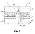
- FIG. 3is a rear view of a pair of the electronic modules of FIGS. 1 and 2 adjacent one another sharing a common receptacle cage wall;
- FIG. 4is an exploded view of components of the electronic module of FIGS. 1 and 2 illustrating a first step in an assembly process
- FIG. 5is as exploded view of components of the electronic module of FIGS. 1 to 2 illustrating a second step in the assembly process
- FIG. 6is as exploded view of components of the electronic module of FIGS. 1 to 2 illustrating a third step in the assembly process
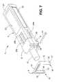
- FIG. 7is as exploded view of components of the electronic module of FIGS. 1 to 2 illustrating a fourth step in the assembly process
- FIG. 8is as exploded view of components of the electronic module of FIGS. 1 to 2 illustrating a fifth step in the assembly process.
- FIG. 9is a perspective view of a copper transceiver patch cable including the electronic module of FIGS. 1 and 2 on either end thereof.
- a pluggable electronic module 1includes a generally rectangular housing 2 , a printed circuit board 3 longitudinally extending in the housing 2 , a hot-pluggable electrical connector 4 extending from the rear of the housing 2 , and a cable connector 5 mounted on the front of the housing 2 .
- the rear electrical connector 4can take any suitable form depending upon the type of mating electrical connector on a host printed circuit board; however, the illustrated card edge connector is preferred.
- the illustrated front cable connector 5is in the form of a block for receiving a multi-conductor cable 10 soldered to the printed circuit board 3 ; however, other front cable connectors can be provided depending upon the function of the module 1 , e.g.
- a bi-directional opto-electronic transceiverrequires a duplex optical connector (LC or SC), a uni-directional opto-electronic module requires a single (LC or SC) connector.
- Conventional transceiverswould also include some form of electro-optical converter, e.g. a photo-detector and/or a laser; however, copper transceivers do not.
- the electronic module 1is slid into a host receptacle, e.g. a cage or guide rail, system with an electrical connector corresponding to the electrical connector 4 , which are mounted on the host printed circuit board in a host device.
- a de-latching mechanism 6is mounted on the bottom of the housing 2 , and includes a latch 7 pivotally connected proximate the middle thereof to the housing 2 about a first axis defined by a first pivoting pin 8 .
- a leverpreferably in the form of a bail handle 9 , extends around the front end of the housing 2 , and is pivotally connected to a first end of the latch 7 about a second axis, parallel to the first axis, defined by a second pivoting pin 11 .
- the bail handle 9includes a pair of side arms 12 and 13 , lower ends of which are pivotally connected to the second pivoting pin 11 , and upper ends of which are connected to a cross bar 14 extending therebetween.
- the bail handle 9can be replaced by a single arm or other form of lever.
- An eccentric projection 16extends substantially perpendicularly from each of the lower ends of the side arms 12 and 13 , and includes a lower rounded surface 17 and an upper flat camming surface 18 (see FIG. 7 ).
- Each projection 16extends into a recessed area 19 , in the housing 2 , which includes an abutment surface.
- the recessed area 19is a rectangular step or indentation formed in the front end of the housing 2 , e.g. in the lower front corners of the cable connector block 5 .
- the lower rounded surface 17enables the projection 16 , and therefore the bail handle 9 , to act like a first class lever and rotate about the second axis, i.e.
- the bail handle 9is not only able to pivot about the second axis; but, further force on the bail handle 9 causes the bail handle 9 to pivot about a third axis defined by the intersection of the camming surface 18 and the abutment surface.
- the bail handle 9also becomes a second class lever with the fulcrum at the intersection of the camming surface 18 and the abutment surface, whereby any added force on the bail handle 9 is applied through the pivot pin 11 to the first end of the latch 7 , thereby pivoting the first end of the latch away from the housing 2 .
- a second end of the latch 7includes a release arm 20 with a latching finger 21 , which engages a corresponding latching opening on the host cage or guide rail system. Pivoting the first end of the latch 7 away from the housing 2 into a release position ( FIG.
- the release arm 20 and the latching finger 21causes the release arm 20 and the latching finger 21 to detract into an opening in the housing 2 , thereby releasing the latching finger 21 from the latching opening on the host cage enabling the transceiver 1 to be removed therefrom.
- the latch 7In the latched position, the latch 7 is recessed into the housing 2 with only the latching finger 21 extending outwardly therefrom.
- the unlatched or release positionthe first end of the latch 7 is pivoted outwardly from the housing 2 , while the latching finger 21 is detracted further into the housing body, whereby the latching finger 21 no longer extends therefrom.
- the housing 2is formed by a housing bottom 22 and a housing top 23 , joined approximately along a midline of the housing 2 .
- the housing bottom 22 and the housing top 23are at least partially formed from a conductive material, and preferably comprise cast metal.
- a solid rectangular conductive projection 25 aextends outwardly from a side of the housing bottom 22 for contacting the host receptacle and providing electromagnetic interference (EMI) protection.
- the projection 25 aextends rearwardly from the cable connector 5 longitudinally along the side of the housing bottom 22 .
- the projection 25 aincludes a sloped rear ramp portion at a leading edge thereof, which gradually decreases in height from the front to the back of the housing 2 to facilitate insertion of the module into a host receptacle, whereby the walls of the cage will engage the ramp portion first and gradually ride up the ramp portion to the main body of the projections.
- solid rectangular projections 25 b and 25 csimilar to projection 25 a , extend longitudinally along the top of a housing top 23 for contacting a top portion of a host receptacle.
- Another projection 25 dextends along a side of the housing top 23 , i.e. the opposite side to the projection 25 a , for added EMI protection.
- Projections 25 a and 25 dmake the width to the housing 2 slightly larger than the width of the host receptacle, whereby the projections 25 a and 25 d frictionally engage the sides of the host receptacle.
- no projectionsare provided on the bottom of the housing bottom 22 , which slides on the host printed circuit board, parallel thereto, during insertion.
- the sides of the housing top 23 and the housing bottom 22are substantially perpendicular to the host printed circuit board.
- a plurality of electronic modulescan be disposed side-by-side, with the adjacent electronic modules 41 and 42 sharing the same cage wall 43 .
- electronic modulesare equipped with projections 25 a and 25 d at the same height and position on both sides of the housing 2 , i.e. same horizontal plane, insertion and extraction of the modules 1 becomes very difficult as the projections 25 a on one side tend to bend the walls of the cage outwardly into the space designated for the projection of the adjacent module. Accordingly, the walls of the host receptacle will squeeze the module therebetween, requiring excessive force for insertion or extraction.
- a solution to the problemis to vertically offset the projections 25 a and 25 d on opposite sides of each housing 2 , so that the projections 25 a and 25 d are not in the same horizontal plane.
- a simple way to provide this vertical offsetis to provide the projection 25 a on one side of the housing bottom 23 , and to provide the projection 25 d on the opposite side of the housing top 22 .
- the lower projection 25 a of the module 41is not directly adjacent the upper projection 25 d of the module 42 , thereby enabling the cage side wall 43 to bend in two vertically spaced apart places.
- the electronic module 1in the form of a copper transceiver, is assembled by first connecting, e.g. soldering, an end of the multi-conductor cable 10 to the printed circuit board 3 , and mounting the assembly into either the housing bottom 22 or the housing top 23 .
- the housing top 23includes a thin tail section 24 , and a pair of generally rectangular tapering ears 26 , i.e. tenons, extending therefrom for mating with the housing bottom 22 .
- the tail section 24has smaller dimensions, i.e. length and width, than the remainder of the housing top 23 .
- a U-shaped bar 27extends across the back of the housing bottom 22 providing a bearing surface and a hold-down bar for the thin tail section 24 of the housing top 23 .
- the tail section 24is inserted under the bar 27 , and the housing top 23 is rotated down until the ears 26 are received in mating recesses 28 , i.e. mortises, in the housing bottom 22 (see FIG. 5 ).
- the first pin 8is then inserted through holes 29 in the sides of the housing bottom 22 , through holes in the ears 26 , and through a bushing extending across the middle of the latch 7 , thereby securing the housing top 23 to the housing bottom 22 , and pivotally mounting the latch 7 to the housing bottom 22 .
- Some form of springe.g. coil spring 31 , is positioned between the release arm 20 and the housing bottom 22 to spring bias the release arm 20 into a latched position, whereby a sufficient force must be applied to the bail handle 9 to overcome the spring force of the spring 31 to pivot the latch 7 into an unlatched or release position.
- the next step in the assemblyincludes the insertion of the second pivoting pin 11 through a hole in the lower end of the side arm 12 , through a bushing in the first end of the latch 7 , and through a hole in the lower end of the side arm 13 .
- the first and second pivoting pins 8 and 11are identical to each other to simplify the supply and the assembly processes.
- the first and second pivoting pins 8 and 11are tapered at the insertion end to facilitate insertion and part alignment, and have a flattened head at the other end for engaging a recessed annular wall in the countersunk hole 29 .
- the cross section of the first and second pivoting pins 8 and 11changes from circular to oblong or oval, so that the major diameter of the oval is large enough to form a slight press fit with the holes 29 at the wall of the housing bottom 22 and of the side arm 12 . Accordingly, the final assembly step, see FIG.
- first and second pivoting pins 8is forcing the in head end of the first and second pivoting pins 8 and 11 into engagement with the side of the housing bottom 22 and the side arm 12 , respectively.
- the first and second pivoting pins 8 and 11can be pressed out, if necessary, without damaging the housing bottom 22 or the first and second pivoting pins 8 and 11 , to facilitate repair or the recycling of parts.
- a patch cable 35comprises the multi-conductor electrical cable 10 and copper transceivers 1 ′ and 1 ′′, similar to electronic module 1 , on either end thereof.
- Each of the copper transceivers 1 ′ and 1 ′′includes the delatching mechanism 6 , as hereinbefore described with reference to FIGS. 1 to 7 . Since the cable 10 is permanently installed inside the copper transceivers 1 ′ and 1 ′′, it is imperative that each bail lever 9 need only be rotated through a small angle, e.g. 5° to 45°, preferably 10° to 30°, before unlatching the latch 7 , as the cable 10 prevents the bail lever 9 from reaching a horizontal position.
Landscapes
- Details Of Connecting Devices For Male And Female Coupling (AREA)
Abstract
Description
- a housing for at least partially enclosing the electronic module, and being at least partially electrically conductive;
- a printed circuit board mounted within the housing having an electrical connector at one end thereof for electrically connecting the module to a mating connector in the host receptacle;
- a latch extending from the housing for releasably holding the module in the host receptacle;
- first and second conductive projections extending from opposite sides of the housing for contacting side walls of the host receptacle;
- wherein the first and second conductive projections are vertically offset, whereby no two conductive projections are in the same horizontal plane.
Claims (20)
Priority Applications (1)
| Application Number | Priority Date | Filing Date | Title |
|---|---|---|---|
| US11/259,291US7056156B1 (en) | 2004-12-06 | 2005-10-26 | Vertically offset EMI projections |
Applications Claiming Priority (2)
| Application Number | Priority Date | Filing Date | Title |
|---|---|---|---|
| US63364304P | 2004-12-06 | 2004-12-06 | |
| US11/259,291US7056156B1 (en) | 2004-12-06 | 2005-10-26 | Vertically offset EMI projections |
Publications (2)
| Publication Number | Publication Date |
|---|---|
| US7056156B1true US7056156B1 (en) | 2006-06-06 |
| US20060121794A1 US20060121794A1 (en) | 2006-06-08 |
Family
ID=36568833
Family Applications (1)
| Application Number | Title | Priority Date | Filing Date |
|---|---|---|---|
| US11/259,291Expired - Fee RelatedUS7056156B1 (en) | 2004-12-06 | 2005-10-26 | Vertically offset EMI projections |
Country Status (1)
| Country | Link |
|---|---|
| US (1) | US7056156B1 (en) |
Cited By (7)
| Publication number | Priority date | Publication date | Assignee | Title |
|---|---|---|---|---|
| WO2008067489A3 (en)* | 2006-11-30 | 2008-07-17 | Finisar Corp | Latching mechanism for a module |
| US20100330841A1 (en)* | 2009-06-24 | 2010-12-30 | Hon Hai Precision Industry Co., Ltd. | Cable connector for terminating different types of cables |
| US20120288240A1 (en)* | 2010-12-14 | 2012-11-15 | Sumitomo Electric Industries, Ltd. | Optical transceiver with finger tightly fastened to housing |
| US20140235091A1 (en)* | 2011-09-16 | 2014-08-21 | HARTING Electronics GmbH | Locking device for electrical connectors |
| US20140307400A1 (en)* | 2013-04-10 | 2014-10-16 | International Business Machines Corporation | Latching cam handle assembly for securing mated circuit boards |
| US10193268B1 (en)* | 2017-10-31 | 2019-01-29 | Teralux Technology Co., Ltd. | SFP cable connector capable of protecting solder joints |
| US11098738B2 (en)* | 2018-01-02 | 2021-08-24 | Delta Electronics, Inc. | Transceiver module |
Families Citing this family (7)
| Publication number | Priority date | Publication date | Assignee | Title |
|---|---|---|---|---|
| JP4643423B2 (en)* | 2005-12-01 | 2011-03-02 | 富士通コンポーネント株式会社 | Cable connector type transceiver module |
| US7351090B1 (en)* | 2006-11-30 | 2008-04-01 | Finisar Corporation | Latching mechanism for a module |
| US7557305B2 (en)* | 2007-11-01 | 2009-07-07 | Nextronics Engineering Corp. | Connector housing for a small and portable transmitting-receiving module |
| CN102377078B (en)* | 2010-08-16 | 2015-05-06 | 富士康(昆山)电脑接插件有限公司 | Connector |
| CN201966402U (en)* | 2010-12-08 | 2011-09-07 | 富士康(昆山)电脑接插件有限公司 | Cable connector |
| US9210817B2 (en)* | 2014-02-03 | 2015-12-08 | Tyco Electronics Corporation | Pluggable module |
| WO2016018345A1 (en)* | 2014-07-31 | 2016-02-04 | Hewlett-Packard Development Company, L.P. | Next generation form factor (ngff) carrier |
Citations (13)
| Publication number | Priority date | Publication date | Assignee | Title |
|---|---|---|---|---|
| US5767999A (en) | 1996-05-02 | 1998-06-16 | Vixel Corporation | Hot-pluggable/interchangeable circuit module and universal guide system having a standard form factor |
| US5766041A (en) | 1996-05-31 | 1998-06-16 | The Whitaker Corporation | Shield member for panel mount connector |
| US6201704B1 (en) | 1995-01-13 | 2001-03-13 | Stratos Lightwave, Inc. | Transceive module with EMI shielding |
| US6206730B1 (en) | 1999-02-04 | 2001-03-27 | Molex Incorporated | Shielded electrical connector |
| US6220878B1 (en) | 1995-10-04 | 2001-04-24 | Methode Electronics, Inc. | Optoelectronic module with grounding means |
| US6416361B1 (en) | 2001-11-16 | 2002-07-09 | Hon Hai Precision Ind. Co., Ltd. | Small form-factor pluggable transceiver cage |
| US6604964B2 (en)* | 2001-01-31 | 2003-08-12 | Tyco Electronics Amp K.K. | Shielded connector assembly |
| US6607308B2 (en) | 2001-02-12 | 2003-08-19 | E20 Communications, Inc. | Fiber-optic modules with shielded housing/covers having mixed finger types |
| US6623307B2 (en)* | 2001-11-08 | 2003-09-23 | Hon Hai Precision Ind. Co., Ltd. | High frequency modular jack connector |
| US6874953B2 (en)* | 2001-02-12 | 2005-04-05 | Jds Uniphase Corporation | Methods and apparatus for fiber-optic modules with shielded housings/covers with fingers |
| US6878872B2 (en) | 2003-03-31 | 2005-04-12 | Molex Incorporated | Shielding cage with multiple module-receiving bays |
| US6884937B1 (en)* | 2003-10-08 | 2005-04-26 | Nortel Networks Limited | Electromagnetic compliant shield having electrostatic discharge protection |
| US6943287B2 (en) | 2003-03-31 | 2005-09-13 | Molex Incorporated | Shielding cage with improved EMI shielding gasket construction |
Family Cites Families (1)
| Publication number | Priority date | Publication date | Assignee | Title |
|---|---|---|---|---|
| US5716361A (en)* | 1995-11-02 | 1998-02-10 | Masini; Michael A. | Bone cutting guides for use in the implantation of prosthetic joint components |
- 2005
- 2005-10-26USUS11/259,291patent/US7056156B1/ennot_activeExpired - Fee Related
Patent Citations (13)
| Publication number | Priority date | Publication date | Assignee | Title |
|---|---|---|---|---|
| US6201704B1 (en) | 1995-01-13 | 2001-03-13 | Stratos Lightwave, Inc. | Transceive module with EMI shielding |
| US6220878B1 (en) | 1995-10-04 | 2001-04-24 | Methode Electronics, Inc. | Optoelectronic module with grounding means |
| US5767999A (en) | 1996-05-02 | 1998-06-16 | Vixel Corporation | Hot-pluggable/interchangeable circuit module and universal guide system having a standard form factor |
| US5766041A (en) | 1996-05-31 | 1998-06-16 | The Whitaker Corporation | Shield member for panel mount connector |
| US6206730B1 (en) | 1999-02-04 | 2001-03-27 | Molex Incorporated | Shielded electrical connector |
| US6604964B2 (en)* | 2001-01-31 | 2003-08-12 | Tyco Electronics Amp K.K. | Shielded connector assembly |
| US6607308B2 (en) | 2001-02-12 | 2003-08-19 | E20 Communications, Inc. | Fiber-optic modules with shielded housing/covers having mixed finger types |
| US6874953B2 (en)* | 2001-02-12 | 2005-04-05 | Jds Uniphase Corporation | Methods and apparatus for fiber-optic modules with shielded housings/covers with fingers |
| US6623307B2 (en)* | 2001-11-08 | 2003-09-23 | Hon Hai Precision Ind. Co., Ltd. | High frequency modular jack connector |
| US6416361B1 (en) | 2001-11-16 | 2002-07-09 | Hon Hai Precision Ind. Co., Ltd. | Small form-factor pluggable transceiver cage |
| US6878872B2 (en) | 2003-03-31 | 2005-04-12 | Molex Incorporated | Shielding cage with multiple module-receiving bays |
| US6943287B2 (en) | 2003-03-31 | 2005-09-13 | Molex Incorporated | Shielding cage with improved EMI shielding gasket construction |
| US6884937B1 (en)* | 2003-10-08 | 2005-04-26 | Nortel Networks Limited | Electromagnetic compliant shield having electrostatic discharge protection |
Cited By (10)
| Publication number | Priority date | Publication date | Assignee | Title |
|---|---|---|---|---|
| WO2008067489A3 (en)* | 2006-11-30 | 2008-07-17 | Finisar Corp | Latching mechanism for a module |
| US20100330841A1 (en)* | 2009-06-24 | 2010-12-30 | Hon Hai Precision Industry Co., Ltd. | Cable connector for terminating different types of cables |
| US20120288240A1 (en)* | 2010-12-14 | 2012-11-15 | Sumitomo Electric Industries, Ltd. | Optical transceiver with finger tightly fastened to housing |
| US9039300B2 (en)* | 2010-12-14 | 2015-05-26 | Sumitomo Electric Industries, Ltd. | Optical transceiver with finger tightly fastened to housing |
| US20140235091A1 (en)* | 2011-09-16 | 2014-08-21 | HARTING Electronics GmbH | Locking device for electrical connectors |
| US9219333B2 (en)* | 2011-09-16 | 2015-12-22 | HARTING Electronics GmbH | Locking device for electrical connectors |
| US20140307400A1 (en)* | 2013-04-10 | 2014-10-16 | International Business Machines Corporation | Latching cam handle assembly for securing mated circuit boards |
| US8976536B2 (en)* | 2013-04-10 | 2015-03-10 | Lenovo Enterprise Solutions (Singapore) Pte. Ltd. | Latching cam handle assembly for securing mated circuit boards |
| US10193268B1 (en)* | 2017-10-31 | 2019-01-29 | Teralux Technology Co., Ltd. | SFP cable connector capable of protecting solder joints |
| US11098738B2 (en)* | 2018-01-02 | 2021-08-24 | Delta Electronics, Inc. | Transceiver module |
Also Published As
| Publication number | Publication date |
|---|---|
| US20060121794A1 (en) | 2006-06-08 |
Similar Documents
| Publication | Publication Date | Title |
|---|---|---|
| US7090527B2 (en) | Transceiver delatching mechanism | |
| US10847930B2 (en) | Asymmetric latches for pluggable transceivers | |
| CN100508298C (en) | Transceiver Module Assembly Release Mechanism | |
| US6304436B1 (en) | Connector system with outwardly opening door for a removable transceiver module | |
| US6890206B2 (en) | Optical transceiver latch | |
| US6980437B2 (en) | Pluggable electronic receptacle with heat sink assembly | |
| US7056156B1 (en) | Vertically offset EMI projections | |
| US7229317B2 (en) | Shielding tabs for reduction of electromagnetic interference | |
| US7296937B1 (en) | Transceiver module assembly with unlatch detection switch | |
| US7794241B2 (en) | Straddle mount connector for pluggable transceiver module | |
| US20100178790A1 (en) | Receptacle connector for a transceiver assembly | |
| US8545234B2 (en) | Electrical connector for a pluggable transceiver module | |
| KR20120063500A (en) | Combined optical and electrical interface | |
| US7433193B2 (en) | Techniques for controlling a position of a transceiver module relative to a connector | |
| CN110417474A (en) | optical transceiver | |
| US7377702B2 (en) | Cageless, pluggable optoelectronic device which enables belly-to-belly layouts | |
| US20250189737A1 (en) | Biased connector system | |
| US7204710B1 (en) | SFP module mounting structure | |
| US20120170890A1 (en) | Miniature Pluggable Video Module | |
| US7175475B2 (en) | Receptacle for copper wire transceivers | |
| US20060056774A1 (en) | Pluggable optical transceiver module assembly | |
| US11177594B2 (en) | Housing for pluggable module | |
| US9583862B1 (en) | Connector assembly and retention mechanism configured to maintain a mated relationship | |
| US9176290B2 (en) | Miniature pluggable video module | |
| CN209497047U (en) | Hot swap type interface connector |
Legal Events
| Date | Code | Title | Description |
|---|---|---|---|
| AS | Assignment | Owner name:JDS UNIPHASE CORPORATION, CALIFORNIA Free format text:ASSIGNMENT OF ASSIGNORS INTEREST;ASSIGNORS:HANLEY, MICHAEL FRANCIS;MOON, JAMES ROBERT;KRUGER, BRUCE P.;AND OTHERS;REEL/FRAME:017148/0499;SIGNING DATES FROM 20051014 TO 20051017 | |
| FPAY | Fee payment | Year of fee payment:4 | |
| FPAY | Fee payment | Year of fee payment:8 | |
| AS | Assignment | Owner name:LUMENTUM OPERATIONS LLC, CALIFORNIA Free format text:ASSIGNMENT OF ASSIGNORS INTEREST;ASSIGNOR:JDS UNIPHASE CORPORATION;REEL/FRAME:036420/0340 Effective date:20150731 | |
| FEPP | Fee payment procedure | Free format text:PAYOR NUMBER ASSIGNED (ORIGINAL EVENT CODE: ASPN); ENTITY STATUS OF PATENT OWNER: LARGE ENTITY | |
| AS | Assignment | Owner name:LUMENTUM OPERATIONS LLC, CALIFORNIA Free format text:CORRECTIVE ASSIGNMENT TO CORRECT THE PATENTS LISTED ON PAGE A-A33 PREVIOUSLY RECORDED ON REEL 036420 FRAME 0340. ASSIGNOR(S) HEREBY CONFIRMS THE PATENT NUMBERS 7,868,247 AND 6,476,312 WERE LISTED IN ERROR AND SHOULD BE REMOVED;ASSIGNOR:JDS UNIPHASE CORPORATION;REEL/FRAME:037562/0513 Effective date:20150731 Owner name:LUMENTUM OPERATIONS LLC, CALIFORNIA Free format text:CORRECTIVE ASSIGNMENT TO CORRECT INCORRECT PATENTS 7,868,247 AND 6,476,312 ON PAGE A-A33 PREVIOUSLY RECORDED ON REEL 036420 FRAME 0340. ASSIGNOR(S) HEREBY CONFIRMS THE ASSIGNMENT;ASSIGNOR:JDS UNIPHASE CORPORATION;REEL/FRAME:037562/0513 Effective date:20150731 | |
| AS | Assignment | Owner name:LUMENTUM OPERATIONS LLC, CALIFORNIA Free format text:CORRECTIVE ASSIGNMENT TO CORRECT THE PATENTS LISTED ON PAGE A-A33 PATENT NUMBERS 7,868,247 AND 6,476,312 WERE LISTED IN ERROR AND SHOULD BE REMOVED. PREVIOUSLY RECORDED ON REEL 036420 FRAME 0340. ASSIGNOR(S) HEREBY CONFIRMS THE ASSIGNMENT;ASSIGNOR:JDS UNIPHASE CORPORATION;REEL/FRAME:037627/0641 Effective date:20150731 Owner name:LUMENTUM OPERATIONS LLC, CALIFORNIA Free format text:CORRECTIVE ASSIGNMENT TO CORRECT PATENTS 7,868,247 AND 6,476,312 LISTED ON PAGE A-A33 PREVIOUSLY RECORDED ON REEL 036420 FRAME 0340. ASSIGNOR(S) HEREBY CONFIRMS THE ASSIGNMENT;ASSIGNOR:JDS UNIPHASE CORPORATION;REEL/FRAME:037627/0641 Effective date:20150731 | |
| FEPP | Fee payment procedure | Free format text:PAYER NUMBER DE-ASSIGNED (ORIGINAL EVENT CODE: RMPN); ENTITY STATUS OF PATENT OWNER: LARGE ENTITY Free format text:PAYOR NUMBER ASSIGNED (ORIGINAL EVENT CODE: ASPN); ENTITY STATUS OF PATENT OWNER: LARGE ENTITY | |
| FEPP | Fee payment procedure | Free format text:MAINTENANCE FEE REMINDER MAILED (ORIGINAL EVENT CODE: REM.) | |
| LAPS | Lapse for failure to pay maintenance fees | Free format text:PATENT EXPIRED FOR FAILURE TO PAY MAINTENANCE FEES (ORIGINAL EVENT CODE: EXP.) | |
| STCH | Information on status: patent discontinuation | Free format text:PATENT EXPIRED DUE TO NONPAYMENT OF MAINTENANCE FEES UNDER 37 CFR 1.362 | |
| FP | Lapsed due to failure to pay maintenance fee | Effective date:20180606 |