US7055127B2 - Mask data preparation - Google Patents
Mask data preparationDownload PDFInfo
- Publication number
- US7055127B2 US7055127B2US10/694,474US69447403AUS7055127B2US 7055127 B2US7055127 B2US 7055127B2US 69447403 AUS69447403 AUS 69447403AUS 7055127 B2US7055127 B2US 7055127B2
- Authority
- US
- United States
- Prior art keywords
- shapes
- mask
- layout
- polygon
- smaller
- Prior art date
- Legal status (The legal status is an assumption and is not a legal conclusion. Google has not performed a legal analysis and makes no representation as to the accuracy of the status listed.)
- Expired - Lifetime, expires
Links
- 238000000034methodMethods0.000claimsabstractdescription56
- 238000012937correctionMethods0.000claimsabstractdescription54
- 238000004519manufacturing processMethods0.000claimsabstractdescription36
- 230000000694effectsEffects0.000claimsdescription35
- 238000013467fragmentationMethods0.000claimsdescription12
- 238000006062fragmentation reactionMethods0.000claimsdescription12
- 230000005855radiationEffects0.000claimsdescription11
- 230000002238attenuated effectEffects0.000claimsdescription5
- 239000000463materialSubstances0.000claimsdescription5
- 239000004065semiconductorSubstances0.000claimsdescription5
- 238000007689inspectionMethods0.000claimsdescription3
- 238000013500data storageMethods0.000claimsdescription2
- 230000003287optical effectEffects0.000abstractdescription13
- 235000012431wafersNutrition0.000description24
- 238000012986modificationMethods0.000description9
- 230000004048modificationEffects0.000description9
- 230000008901benefitEffects0.000description8
- 230000008569processEffects0.000description8
- 238000013459approachMethods0.000description5
- 238000005286illuminationMethods0.000description5
- 238000012545processingMethods0.000description5
- 230000004075alterationEffects0.000description3
- 230000005540biological transmissionEffects0.000description3
- 238000013461designMethods0.000description3
- 238000001459lithographyMethods0.000description3
- 238000000206photolithographyMethods0.000description3
- 230000011218segmentationEffects0.000description3
- 239000000758substrateSubstances0.000description3
- 230000007423decreaseEffects0.000description2
- 238000002224dissectionMethods0.000description2
- 238000011156evaluationMethods0.000description2
- 238000012546transferMethods0.000description2
- 239000011800void materialSubstances0.000description2
- VYZAMTAEIAYCRO-UHFFFAOYSA-NChromiumChemical compound[Cr]VYZAMTAEIAYCRO-UHFFFAOYSA-N0.000description1
- 230000001154acute effectEffects0.000description1
- 238000006243chemical reactionMethods0.000description1
- 239000011248coating agentSubstances0.000description1
- 238000000576coating methodMethods0.000description1
- 238000004891communicationMethods0.000description1
- 230000000295complement effectEffects0.000description1
- 238000010276constructionMethods0.000description1
- 230000003247decreasing effectEffects0.000description1
- 230000001066destructive effectEffects0.000description1
- 238000010586diagramMethods0.000description1
- 238000006073displacement reactionMethods0.000description1
- 238000001312dry etchingMethods0.000description1
- 238000002513implantationMethods0.000description1
- 230000007246mechanismEffects0.000description1
- 239000010453quartzSubstances0.000description1
- 230000002040relaxant effectEffects0.000description1
- VYPSYNLAJGMNEJ-UHFFFAOYSA-Nsilicon dioxideInorganic materialsO=[Si]=OVYPSYNLAJGMNEJ-UHFFFAOYSA-N0.000description1
- 238000000638solvent extractionMethods0.000description1
- 238000001228spectrumMethods0.000description1
- 238000012795verificationMethods0.000description1
Images


Classifications
- G—PHYSICS
- G03—PHOTOGRAPHY; CINEMATOGRAPHY; ANALOGOUS TECHNIQUES USING WAVES OTHER THAN OPTICAL WAVES; ELECTROGRAPHY; HOLOGRAPHY
- G03F—PHOTOMECHANICAL PRODUCTION OF TEXTURED OR PATTERNED SURFACES, e.g. FOR PRINTING, FOR PROCESSING OF SEMICONDUCTOR DEVICES; MATERIALS THEREFOR; ORIGINALS THEREFOR; APPARATUS SPECIALLY ADAPTED THEREFOR
- G03F1/00—Originals for photomechanical production of textured or patterned surfaces, e.g., masks, photo-masks, reticles; Mask blanks or pellicles therefor; Containers specially adapted therefor; Preparation thereof
- G03F1/36—Masks having proximity correction features; Preparation thereof, e.g. optical proximity correction [OPC] design processes
- G—PHYSICS
- G03—PHOTOGRAPHY; CINEMATOGRAPHY; ANALOGOUS TECHNIQUES USING WAVES OTHER THAN OPTICAL WAVES; ELECTROGRAPHY; HOLOGRAPHY
- G03F—PHOTOMECHANICAL PRODUCTION OF TEXTURED OR PATTERNED SURFACES, e.g. FOR PRINTING, FOR PROCESSING OF SEMICONDUCTOR DEVICES; MATERIALS THEREFOR; ORIGINALS THEREFOR; APPARATUS SPECIALLY ADAPTED THEREFOR
- G03F1/00—Originals for photomechanical production of textured or patterned surfaces, e.g., masks, photo-masks, reticles; Mask blanks or pellicles therefor; Containers specially adapted therefor; Preparation thereof
- G03F1/68—Preparation processes not covered by groups G03F1/20 - G03F1/50
Definitions
- the inventionrelates to the process of fabricating semiconductor chips. More specifically, the invention relates to a method for preparing mask data.
- the high volume manufacturing of integrated circuitsrelies on the use of optical lithography to define the features printed on the semiconductor chips.
- the lithography processstarts first by coating the surface of the semiconductor wafer with a material called resist. A source of radiation is then shone through the mask in the case of a transparent mask. For a reflective mask the radiation is reflected by the mask.
- the transparent maskis made of a substrate transparent to the radiation and coated with a patterned opaque layer defining clear and opaque regions to the radiation.
- Transparent masksare mostly used in optical lithography with typical wavelengths of 436 nm, 405 nm, 365 nm, 248 nm, 193 nm, and 157 nm.
- the reflective masksare made using a substrate reflective to the radiation and coated with a patterned non-reflective layer defining reflective and non-reflective regions to the radiation.
- a reflective maskcould be made of a non-reflective substrate coated with a reflective layer. Reflective masks are mostly used for shorter radiation wavelength on the order of 13 nm usually referred to as EUV or Extreme Ultra Violet.
- an image of the maskis formed using an optical system on top of the resist layer.
- Various optical systemscan be used to produce an image of the mask.
- the main technique used today in volume productionrelies on the projection of the image of the mask onto the wafer.
- the wafer imageis reduced by a factor of 4 (usually named mask image magnification factor or wafer image demagnification factor) as compared to the mask image, thus relaxing the mask fabrication requirements.
- the field on the wafer corresponding to the image of the maskis exposed multiple times to cover the entire wafer. The entire field can be exposed in one shot, in this case the equipment is named a stepper.
- the fieldcan be scanned by moving the mask and the wafer relative to the projection lens.
- the equipmentis named a scanner.
- Scannersoffer the advantage to mitigate some field non-uniformities observed in steppers but the scanning mechanism adds residual noise that partially degrades the aerial image.
- scannersshow differences of the aerial image for features perpendicular to the scan direction versus features parallel to the scan direction.
- the resist layeris exposed by the radiation passing through the mask in case of a transparent mask or reflected by the mask in the case of a reflective mask.
- the resistis then developed in a developer bath and depending on the polarity of the resist (positive or negative), the exposed regions or the unexposed regions of the resist are removed.
- the end resultis a semiconductor wafer with a resist layer having a desired pattern. This resist pattern can then be used by subsequent processing steps of the underlying regions of the wafer.
- OPCOptical Proximity Correction
- modifications of the design imageaccount for optical limitations as well as mask fabrication limitations and resist limitations. Modifications of the design image can also account for the subsequent process steps like dry etching or implantation. It can also account for flare in the optical system as well as pattern density variations.
- Another application of proximity effect correctionis the compensation of the effects of aberrations of the optical system used to print the image of the mask onto the wafers. In this case, a mask with aberration correction would be dedicated to a given lithography tool as the aberrations are tool-specific.
- FIG. 1illustrates the modification of the mask data to correct for proximity effects.
- the processing of the mask datastarts with a target layout 101 representing the desired dimensions of the image on the wafer.
- the printed image 102 of the target layout 101differs from the desired image due to proximity effect.
- the target image 101is shown with the printed image 102 .
- the edges of the featuresare then moved ( 103 ) so that the corresponding printed image on the wafer 104 is correct (as close to the target as possible).
- all the areas of the layouthave been corrected but different degrees of proximity effect correction aggressiveness can be applied to different regions depending on the criticality of the region in the integrated circuit.
- the corrections to layout 101can be applied using a rule-based approach or a model-based approach.
- Rule-based OPCthe displacement of the segments would be set by a list of rules depending, for example, on the feature size and its environment.
- model-based OPCthe printed image on the wafer would be simulated using a model of the pattern transfer process. The correction would be set such that the simulated image matches the desired wafer image.
- a combination of rule-based OPC and model-based OPCsometimes referred to as hybrid OPC can also be used.
- the original layout 201 as shown in FIG. 2is dissected in smaller segments 203 shown in modified layout 202 .
- Each segmentis associated an evaluation point 204 .
- the printed errors of the evaluation pointsare compensated by moving the corresponding segment in a direction perpendicular to the segment as shown in the final layout 205 .
- the segmentsare corrected using multiple iterations in order to account for corrections of neighboring segments.
- the image qualitycan be improved by adding printing or non-printing assist features along the edges of the main features.
- These assist featuresmodify the diffraction spectrum of the pattern in a way that improves the printing of the main feature.
- the practical implementation of assist featuresis enhanced with the use of proximity effect correction as described above to correct for any optical printing artifact as well as resist and etch artifacts.
- the image qualitycan also be improved by using phase-shifting masks.
- phase-shifting masksIn this case, at least two different regions are created on the masks corresponding to different phase and transmission of the light either going through these regions (for transparent mask) or reflected by these regions (for reflective mask).
- the phase difference between the two regionsis chosen to be substantially equal to 180 degrees.
- the destructive interference between adjacent regions of opposite phasecreates a very sharp contrast at the boundary between the regions, thus leading to the printing of small features on the wafer.
- Two main classes of phase-shifting masksare in use today. For the first class, the amount of light transmitted for transparent masks (or reflected for reflective masks) by one region is only a portion of the light transmitted (or reflected) by the other region, typically 5% to 15%.
- phase-shifting masksregions opaque to the light source for transparent mask (with low reflection for reflective masks) are kept on the mask.
- regions opaque to the light source for transparent maskare kept on the mask.
- These types of maskare referred to as tri-tone mask as they have for transparent masks, clear regions, opaque regions, and partially transparent regions (non-reflective, reflective, and partially reflective for reflective masks).
- the light transmitted (for transparent masks) or reflected (for reflective masks) by one regionis substantially equal to the light transmitted (for transparent masks) or reflected (for reflective masks) by the other region.
- the second class of masksincludes the following types of phase-shifting masks: alternating aperture phase-shifting masks, chromeless phase-shifting masks, and rim phase-shifting masks.
- phase-shifting masksalternating aperture phase-shifting masks, chromeless phase-shifting masks, and rim phase-shifting masks.
- the practical implementation of these techniquesis improved with the use of proximity effect correction as described above to correct for any optical printing artifact as well as resist and etch artifacts. All the techniques described in this paragraph can also be combined with the use of assist features.
- the image qualitycan also be improved by using off-axis illumination.
- the illuminator of the stepper or scanneris shaped in a way that only the light at certain angles with respect to the optical axis is used to create the image thereby favoring certain spatial frequencies of the mask pattern.
- the off-axis settingcan be adjusted for a given feature size and type or for a collection of feature sizes and types.
- Off-axis illuminationcan be used in combination with binary masks, attenuated phase-shifting masks, chromeless phase-shifting masks, or rim phase-shifting masks. Off-axis illumination will also be improved by the use of proximity effect correction as described in a previous paragraph. Off-axis illumination can also be combined with the use of assist-features.
- anglesare 45 degree, 90 degree and 135 degree angles because of the restriction of the shapes that can be produced by the exposure tool.
- the complexity of the correction after OPCcan create some issue for vector-scan e-beam mask writing tool as very small slivers are created when the data is converted to the mask write tool format as shown in FIG. 3.
- 301represents the data before OPC
- 302the data after OPC
- 303the data after fracturing.
- a sliver 304was created during the fracturing of the data.
- 401represents the data before OPC, 402 the data after OPC and 403 the data after fracturing.
- the data 404represents the same data as 401 rotated by 90 degree clockwise.
- the data 405corresponds to the data 404 after OPC. It should be noted that the data 405 can be obtained by rotating by 90 degree clockwise the data 402 .
- the data 406corresponds to the data 405 after fracturing. In this case 406 cannot be obtained by rotating by 90 degree clockwise the data 403 .
- the fracturing tooldoes not recognize the fact that the structures 402 and 405 are the same except for a 90-degree clockwise rotation and it creates two outputs 403 and 406 with different fracturing shapes.
- the difference in fracturing shapeswill create some dosage difference between 403 and 406 when the photo-mask is exposed and it will result in dimension errors.
- This problemcan be even more acute in critical areas of the layout.
- 401 and 404could represent a portion of a poly level and the dotted line 407 and 408 could represent the corresponding active area.
- the intersections between 401 and 407 (region 409 ), and 404 and 408 (region 410 )represent the gate regions of the poly level whose dimensions are critical for ensuring the proper operation of the transistors.
- the regions corresponding to 409 and 410have been decomposed differently thus creating dimensional difference on the mask because of the nature of the vector scan mask exposure tools.
- a method for performing proximity effect correction on a layout of an integrated circuitis described.
- the methodconsists of fragmenting the polygons of the layout into shapes based upon parameters of a manufacturing tool used for implementing the layout and then performing proximity effect correction on some of the segments of the shapes.
- the manufacturing toolcan be a mask writer or more specifically a vector-scan, e-beam, mask writer.
- the fragmentation of the shapescan be such that no shape larger than the maximum allowable shape size is created after correction or no shape smaller than the minimum allowable shape size is created after correction.
- This methodcan also be used to generate the data needed for various types of masks such as binary masks, attenuated phase-shifting masks, tri-tone phase-shifting masks, and alternating phase-shifting masks.
- alternating phase-shifting maskstwo edges of a given shape may end up abutting two distinct phase-shifting regions and these two regions will need to be out of phase. This information can be stored and used later on when the phase assignment of the shifter regions is performed.
- the manufacturing toolis a mask inspection tool.
- some edges of the shapesare abutting the boundary of a critical area of the layout.
- the position of the boundary between the two shapescan also be adjusted to account for the position of the corrected edges of the shapes.
- polygons within proximity range of a first polygonare taken into account in the fragmentation of the shapes of the first polygon.
- corners of the polygons within proximity rangecan be used.
- Embodiments of the inventioninclude a photolithographic mask.
- the photolithographic maskcomprises a layout pattern that has been corrected for proximity effects using the method described above.
- Embodiments of the inventioninclude a method for manufacturing integrated circuits.
- the methodincludes exposing a layer of material in an integrated circuit using a mask defined above.
- the polarity of the resist used to define the features on the maskis chosen such that the critical regions of the layout correspond to exposed shapes.
- Embodiments of the inventioninclude a method for producing a photolithographic mask.
- the photolithographic maskis fabricated using a mask layout.
- the mask layoutincludes a layout pattern that has been corrected for proximity effects using the method described above.
- Embodiments of the inventioninclude a system for producing a layout.
- the systemincludes a data processor which executes programs of instruction and a memory accessible by the data processor to store programs of instruction.
- the programs of instructioninclude logic to receive the computer readable layout of a portion of the integrated circuit and to correct the layout using the correction method described above.
- Embodiments of the inventioninclude an article of manufacture, comprising a machine readable data storage medium storing programs of instruction.
- the programs of instructioninclude logic to receive a computer readable layout of a portion of the integrated circuit and to correct the layout using the correction method described above.
- Embodiments of the inventioninclude a method for manufacturing integrated circuits. The method includes exposing a layer of material in an integrated circuit using a mask having a mask layout based on the corrected layout described above. In some embodiments, the polarity of the resist used to define the features on the mask is chosen such that the critical regions of the layout correspond to exposed shapes.
- FIG. 1illustrates the modification of the data to correct proximity effects.
- FIG. 2illustrates the process flow used for model-based OPC.
- FIG. 3illustrates the modification of the data to correct proximity effect and to fracture the polygons.
- FIG. 4compares the OPC and fracturing steps for a polygon oriented at 0 and 90 degrees.
- FIG. 5depicts a new methodology where the polygons are fractured first and the OPC step is performed next.
- FIG. 6 adescribes the OPC effects of a maximum inner or outer correction on the shape dimensions.
- FIG. 6 bdescribes the OPC effects on the stitching of the shapes.
- FIG. 7illustrates the advantage of the invention in terms of preventing the creation of slivers and in terms of reducing the number of shapes created.
- FIG. 8illustrates the use of polygons in proximity range to define the fracturing of a given polygon.
- FIG. 9illustrates the notion of shape and the associated edges.
- FIG. 10illustrates the notion of shape and the associated edges for use in phase-shifting mask.
- FIG. 11is a block diagram of a computer system adapted for fracturing, proximity effect correction, and verification according to the present invention.
- FIG. 12is a flow chart for a process of integrated circuit manufacturing according to the present invention.
- FIG. 5A technique described in FIG. 5 was developed to address the issues encountered during the fracturing of data for vector-scan mask writer.
- the polygon 501 before correctionis first fractured in smaller shapes 502 . Some of the edges of the shapes are abutting the original polygon.
- the shapesare modified into 503 and no sliver was created as shown in FIG. 5 .
- Fracturing into shapes before OPCpresents some important advantages.
- the shapescan be chosen such that even with the largest OPC correction, the shape will not turn into a shape difficult to manufacture for the vector-scan e-beam mask writer.
- 601represents a shape after fracturing which is a part of a larger polygon 602 (not completely drawn on the figure).
- the shape 602could receive a maximum inner correction or a maximum outer correction as described in FIG. 6 a .
- 603represents the shape after maximum inner correction
- 604represents the shape after maximum outer correction.
- the advantage of fracturing the shape before OPC as described earlier in FIG. 5is that the dimensions of the shape 601 are chosen such that both cases 603 or 604 can be manufactured reliably using a vector-scan e-beam mask writer.
- the width of 603is larger than the minimum width the vector-scan e-beam mask writer can print reliably, i.e. 603 is not a sliver as shown in FIG. 3 .
- the width of 604is smaller than the maximum width the vector-scan e-beam mask writer can print in one single shot, i.e. the shape does not need to be split into two shapes.
- the fracturing of the shapescan also be optimized for other manufacturing tools besides mask writers like for example mask inspection tools.
- FIG. 6 bshows an example or a corner polygon before correction 605 , after fracturing 606 , and after OPC 607 .
- the shapes in dotted lines in 607represent the shapes before OPC, the solid lines represent the shapes after OPC. Note that the original shape 605 was fractured in two shapes 606 containing a 45-degree angle which are valid shapes for the shaped-beam vector-scan mask writer.
- the advantage of the 45-degree angle in this casei.e. elbow
- the advantage of the 45-degree angle in this caseis that it minimizes the number of shapes created and facilitates the OPC step.
- the 45-degree boundary between the two shapeswas moved after correction to accommodate for the asymmetric OPC, i.e. the shapes have been stitched back together after OPC. Stitching the shapes is important for shaped-beam vector-scan mask writers as no void can be left between the shapes and no overlap is allowed between the shapes. A void would result in no exposure, an overlap would result in double exposure.
- 501can represent a polygon part of the poly level and 504 represents the corresponding active area.
- the intersection between the polygons 501 and 504is the gate region which is the critical area of the poly level as explained earlier in reference to FIG. 4 .
- this critical areawas fractured in exactly two shapes 505 and 506 . Some of the edges of the shapes 505 and 506 are abutting the critical area. The two shapes 505 and 506 are converted respectively into the shapes 507 and 508 after OPC.
- the tolerance on the correction of these shapescan be made tighter, for example, ⁇ 1 nm maximum edge placement error after correction versus ⁇ 3 nm maximum edge placement error for shapes corresponding to non-critical areas of the layout.
- the number of shapes in the critical regionscan be increased compared to non-critical regions in order to achieve a more accurate correction.
- FIG. 7shows the example of a polygon 701 (only a portion of the polygon is represented).
- the polygon 701is corrected into the polygon 702 , which is then fractured into 703 .
- any misalignment of the segmentation on the left edge with regard to the right edgecan potentially create a sliver during subsequent fracturing as shown on 703 .
- the new method described in this applicationsolves the problem by creating fractured shapes before OPC.
- the original polygon 704is fractured into the polygon 705 which is subsequently corrected into the polygon 706 .
- the shapes defined in 705prevent the issue described in 703 . Moreover the total number of shapes can be decreased which in turn will decrease the time it takes to write the mask and the overall cost of manufacturing the mask.
- the fracturing stepcan be tailored to the OPC step requirements.
- the layout 801is fractured into the layout 802 and then turned into the layout 803 after OPC. Since the rectangle 804 is within proximity range of the rectangle 805 , its presence will have an impact on the printing of the rectangle 805 . Therefore, the corners of the rectangle 804 are used as a reference to create the shape 805 since it is likely that the correction along the edge of the rectangle 805 will be different in the proximity of the rectangle 804 . The correction after OPC shows such a difference on the layout 803 . If the shape 806 had not been created the correction between the polygons 804 and 805 would have been incorrect.
- Rectangle 804could belong to the same layer as rectangle 805 or it could belong to a different layer.
- 804could belong to the active area layer and 805 could belong to the gate layer.
- FIGS. 5 , 6 , 7 , and 8emphasize the need to combine OPC parameters and fracturing parameters.
- the segmentation performed during the OPC stepneed to be consistent with the segmentation done at fracturing.
- the usual flow of fracturing the data after performing OPCcan also be improved if the OPC parameters are chosen in such a way that they do not create any issue with the subsequent fracturing step.
- the advantage of fracturing firsti.e. before the OPC step
- the shapesare defined first and the creation of small slivers as described in FIG. 5 can be avoided by making sure that the shape dimension is compatible with the maximum OPC correction (described in FIG. 6 a ).
- the datais represented in a hierarchical fashion in order to minimize the amount of data needed to describe the circuitry.
- the hierarchical tree obtainedis made of cells containing data and placement of other cells.
- hierarchical fracturingwill be required.
- One of the hurdles to the implementation of hierarchical fracturingis the need for partitioning the layout into fields required by the vector-scan e-beam mask writers. At the boundaries of these fields, or for some mask writer in the vicinity of the boundaries, the polygons should be cut.
- two placements of a cell in two different environments with a different fracturing boundarywill have to be named differently since the fracturing result of the cell could be different.
- the layout data or a reverse-tone image of the layout datawill be needed. If the layout data represents areas of the mask that should be dark, the layout data can be fractured directly to expose the mask with a negative-tone resist. On the other hand, the reverse-tone image of the layout data will be needed to expose the mask with a positive tone resist. If the layout data represents areas of the mask that should be clear (quartz), the layout data can be fractured directly to expose the mask with a positive-tone resist. On the other hand, the reverse-tone image of the layout data will be needed to expose the mask with a negative tone resist. The technique of this invention works for both cases.
- the resist polarity used to fabricate the maskwill be chosen to minimize the volume of data, i.e. the number of shapes.
- the resist polarityshould be chosen in such a way that the critical dimensions of the layout are defined by exposed shapes.
- a negative tone resistshould be used to manufacture the mask to obtain a dark (chrome) 503 representation. If a positive tone resist were used the data volume would considerably increase (the complementary of data 503 would be exposed). Since the regions outside of data 503 are exposed, the size and dimensions of the shapes needed to expose the mask would depend on adjacent patterns. It would therefore be impossible to predict the shapes needed to create the critical gate regions thus creating possible dimensional control issue.
- 507 and 508clearly define the gate region for a negative-tone resist in this specific example thus ensuring a better control of the exposure of the gate region independently of its environment.
- FIG. 9describes how the shapes can be used for subsequent processing steps.
- a shape 902is shown in polygon 901 .
- a magnified view of the shapeis given on the right side of FIG. 9 .
- the shapecan be decomposed in two types of edges, edges that will create a printed edge on the wafer ( 903 ) and edges that will not create a printed edge on the wafer ( 904 , 905 , 906 ). All edges ( 903 , 904 , 905 , 906 ) are important for the fracturing step as they are all required to define the shape.
- edges creating printed edges on the waferare important ( 903 ) as the position of the printed edge is being corrected to reflect the original layout.
- the datacan also be verified to make sure that the printed edge is at the location defined in the original layout. In this case, only the edges creating printed edges on the wafer are important ( 903 ).
- FIG. 10describes how the shapes can be used for phase-shifting the layout.
- a shape 1002is shown in polygon 1001 .
- a magnified view of the shapeis given on the right side of FIG. 10 .
- the shapecan be decomposed in two types of edges, edges that will create a printed edge on the wafer ( 1003 and 1005 ) and edges that will not create a printed edge on the wafer ( 1004 , 1006 ).
- edge 1003 and 1005are adjacent to a shifter region.
- the shifter region adjacent to edge 1003should be out of phase of the shifter region adjacent to edge 1005 .
- the information about the edges 1003 and 1005can be stored and later on used to assign the phase of the phase-shifting regions.
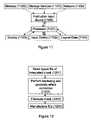
- FIG. 11illustrates a computer system that can be used to fracture the data, applying OPC and verifying the data.
- This computer systemrepresents a wide variety of computer systems and computer architectures suitable for this application.
- a processor 1101is connected to receive data indicating user signals from user input device 1102 and to provide data defining images to display 1103 .
- Processor 1101is also connected for accessing mask layout data 1104 , which define a mask layout under construction and a layout for a layer of material to be exposed using the mask.
- Processor 1101is also connected for receiving instruction data from instruction input device 1105 , which can provide instructions received from connections to memory 1106 , storage medium access device 1107 , or network 1108 .
- FIG. 12illustrates the manufacturing process of an IC (Integrated Circuit).
- the layout file of the integrated circuitis first read using a computer system described in FIG. 11 .
- the layoutis fractured and then corrected for proximity effect.
- the data resulting from step 1202is used to create a mask at step 1203 , and the mask is finally used in the fabrication process of an IC at step 1204 .
- the technique described abovecan also be used to directly create an image on the wafer using tools referred to as “direct-write” tools.
- the direct-write toolcould be an optical tool, an e-beam tool, or and EUV tool.
- the OPC stepwould be replaced by a step including the correction of the proximity effects created by the direct write tool.
- the data structures and code described in this descriptioncan be stored on a computer readable storage medium, which may be any device or medium that can store code and/or data for use by a computer system.
- a computer readable storage mediumwhich includes, but is not limited to, magnetic and optical storage devices such as disk drives, magnetic tapes, CD (compact discs) and DVD (digital video disks), and computer instruction signals embodied in a transmission medium.
- the transmission mediummay include a communication network, such as the Internet.
- the inventioncan be applied to any binary masks, rim phase-shifting masks, chromeless phase-shifting masks, attenuated phase-shifting masks, alternating aperture phase-shifting masks used in single or multiple exposure methodologies.
Landscapes
- Physics & Mathematics (AREA)
- General Physics & Mathematics (AREA)
- Preparing Plates And Mask In Photomechanical Process (AREA)
- Exposure And Positioning Against Photoresist Photosensitive Materials (AREA)
Abstract
Description
Claims (20)
Priority Applications (3)
| Application Number | Priority Date | Filing Date | Title |
|---|---|---|---|
| US10/694,474US7055127B2 (en) | 2003-10-27 | 2003-10-27 | Mask data preparation |
| PCT/US2004/035622WO2005045897A2 (en) | 2003-10-27 | 2004-10-27 | Mask data preparation |
| US11/442,110US7614033B2 (en) | 2003-10-01 | 2006-05-26 | Mask data preparation |
Applications Claiming Priority (1)
| Application Number | Priority Date | Filing Date | Title |
|---|---|---|---|
| US10/694,474US7055127B2 (en) | 2003-10-27 | 2003-10-27 | Mask data preparation |
Related Child Applications (1)
| Application Number | Title | Priority Date | Filing Date |
|---|---|---|---|
| US11/442,110ContinuationUS7614033B2 (en) | 2003-10-01 | 2006-05-26 | Mask data preparation |
Publications (2)
| Publication Number | Publication Date |
|---|---|
| US20050091632A1 US20050091632A1 (en) | 2005-04-28 |
| US7055127B2true US7055127B2 (en) | 2006-05-30 |
Family
ID=34522612
Family Applications (2)
| Application Number | Title | Priority Date | Filing Date |
|---|---|---|---|
| US10/694,474Expired - LifetimeUS7055127B2 (en) | 2003-10-01 | 2003-10-27 | Mask data preparation |
| US11/442,110ActiveUS7614033B2 (en) | 2003-10-01 | 2006-05-26 | Mask data preparation |
Family Applications After (1)
| Application Number | Title | Priority Date | Filing Date |
|---|---|---|---|
| US11/442,110ActiveUS7614033B2 (en) | 2003-10-01 | 2006-05-26 | Mask data preparation |
Country Status (2)
| Country | Link |
|---|---|
| US (2) | US7055127B2 (en) |
| WO (1) | WO2005045897A2 (en) |
Cited By (14)
| Publication number | Priority date | Publication date | Assignee | Title |
|---|---|---|---|---|
| US20060190919A1 (en)* | 2005-02-24 | 2006-08-24 | Texas Instruments Incorporated | Method of locating sub-resolution assist feature(s) |
| US20070085032A1 (en)* | 2005-10-03 | 2007-04-19 | Applied Materials, Inc. | Writing a circuit design pattern with shaped particle beam flashes |
| US20070130558A1 (en)* | 2005-09-26 | 2007-06-07 | Lars Ivansen | Methods and systems for pattern generation based on multiple forms of design data |
| US20090037867A1 (en)* | 2007-08-03 | 2009-02-05 | International Business Machines Corporation | Method for optimization of optical proximity correction |
| US20090046263A1 (en)* | 2007-08-14 | 2009-02-19 | Applied Materials, Inc. | Using phase difference of interference lithography for resolution enhancement |
| WO2009029824A1 (en)* | 2007-08-31 | 2009-03-05 | Applied Materials, Inc. | Resolution enhancement techniques combining interference-assisted lithography with other photolithography techniques |
| US7930653B2 (en) | 2007-04-17 | 2011-04-19 | Micronic Laser Systems Ab | Triangulating design data and encoding design intent for microlithographic printing |
| US20110286658A1 (en)* | 2010-05-24 | 2011-11-24 | Tadashi Mitsui | Pattern inspection method and semiconductor device manufacturing method |
| US20120268813A1 (en)* | 2011-04-21 | 2012-10-25 | Jin-Pil Kim | Mask for black matrix |
| US8769445B2 (en) | 2010-09-22 | 2014-07-01 | International Business Machines Corporation | Method for determining mask operation activities |
| US20140220786A1 (en)* | 2013-02-01 | 2014-08-07 | GlobalFoundries, Inc. | Methods for optical proximity correction in the design and fabrication of integrated circuits |
| US9018108B2 (en) | 2013-01-25 | 2015-04-28 | Applied Materials, Inc. | Low shrinkage dielectric films |
| US20160162624A1 (en)* | 2014-12-09 | 2016-06-09 | GlobalFoundries, Inc. | Methods for optical proximity correction in the design and fabrication of integrated circuits using extreme ultraviolet lithography |
| US11733604B2 (en) | 2020-08-18 | 2023-08-22 | Samsung Electronics Co., Ltd. | Optical proximity correction method and method of fabricating a semiconductor device using the same |
Families Citing this family (38)
| Publication number | Priority date | Publication date | Assignee | Title |
|---|---|---|---|---|
| KR100911595B1 (en)* | 2004-03-09 | 2009-08-07 | 호야 가부시키가이샤 | Method and system for obtaining mask blank information, method for providing mask blank information, method for supporting transfer mask manufacture and manufacturing transfer mask, and method for manufacturing and providing mask blank |
| US7401319B2 (en)* | 2004-12-23 | 2008-07-15 | Invarium, Inc. | Method and system for reticle-wide hierarchy management for representational and computational reuse in integrated circuit layout design |
| US7315999B2 (en)* | 2005-03-17 | 2008-01-01 | Synopsys, Inc. | Method and apparatus for identifying assist feature placement problems |
| US20070083846A1 (en)* | 2005-07-28 | 2007-04-12 | Taiwan Semiconductor Manufacturing Company, Ltd. | Optimized modules' proximity correction |
| KR100732772B1 (en)* | 2006-04-25 | 2007-06-27 | 주식회사 하이닉스반도체 | Mask Layout Formation Method and Layout |
| US7823110B2 (en)* | 2006-09-15 | 2010-10-26 | Softjin Technologies Private Limited | Method and system for processing geometrical layout design data |
| US7444199B2 (en)* | 2006-11-09 | 2008-10-28 | Taiwan Semiconductor Manufacturing Company, Ltd. | Method for preparing mask and wafer data files |
| US7669173B2 (en)* | 2006-12-07 | 2010-02-23 | Infineon Technologies Ag | Semiconductor mask and method of making same |
| US20080168419A1 (en)* | 2007-01-04 | 2008-07-10 | International Business Machines Corporation | Optical proximity correction improvement by fracturing after pre-optical proximity correction |
| US7535044B2 (en)* | 2007-01-31 | 2009-05-19 | Qimonda Ag | Semiconductor device, method for manufacturing a semiconductor device and mask for manufacturing a semiconductor device |
| US20090077519A1 (en)* | 2007-09-17 | 2009-03-19 | Le Hong | Displacement Aware Optical Proximity Correction For Microcircuit Layout Designs |
| JP2009210707A (en)* | 2008-03-03 | 2009-09-17 | Nec Electronics Corp | Photomask, method for designing the same and design program |
| US8369569B2 (en)* | 2008-03-21 | 2013-02-05 | Synopsys, Inc. | Method and apparatus for detecting non-uniform fracturing of a photomask shape |
| KR100955158B1 (en)* | 2008-04-15 | 2010-04-28 | 주식회사 하이닉스반도체 | Optical proximity correction method |
| US7901850B2 (en) | 2008-09-01 | 2011-03-08 | D2S, Inc. | Method and system for design of a reticle to be manufactured using variable shaped beam lithography |
| US9341936B2 (en) | 2008-09-01 | 2016-05-17 | D2S, Inc. | Method and system for forming a pattern on a reticle using charged particle beam lithography |
| US20120219886A1 (en) | 2011-02-28 | 2012-08-30 | D2S, Inc. | Method and system for forming patterns using charged particle beam lithography with variable pattern dosage |
| US9323140B2 (en) | 2008-09-01 | 2016-04-26 | D2S, Inc. | Method and system for forming a pattern on a reticle using charged particle beam lithography |
| US8057970B2 (en) | 2008-09-01 | 2011-11-15 | D2S, Inc. | Method and system for forming circular patterns on a surface |
| US8039176B2 (en) | 2009-08-26 | 2011-10-18 | D2S, Inc. | Method for fracturing and forming a pattern using curvilinear characters with charged particle beam lithography |
| US8669023B2 (en) | 2008-09-01 | 2014-03-11 | D2S, Inc. | Method for optical proximity correction of a reticle to be manufactured using shaped beam lithography |
| US7985514B2 (en)* | 2009-10-21 | 2011-07-26 | D2S, Inc. | Method for fracturing a pattern for writing with a shaped charged particle beam writing system using dragged shots |
| US9448473B2 (en) | 2009-08-26 | 2016-09-20 | D2S, Inc. | Method for fracturing and forming a pattern using shaped beam charged particle beam lithography |
| US20120278770A1 (en) | 2011-04-26 | 2012-11-01 | D2S, Inc. | Method and system for forming non-manhattan patterns using variable shaped beam lithography |
| TWI496182B (en)* | 2009-08-26 | 2015-08-11 | D2S Inc | Method and system for manufacturing surface using charged beam lithography using variable beam blur technique |
| US9164372B2 (en) | 2009-08-26 | 2015-10-20 | D2S, Inc. | Method and system for forming non-manhattan patterns using variable shaped beam lithography |
| US20110089345A1 (en)* | 2009-10-21 | 2011-04-21 | D2S, Inc. | Method and system for manufacturing a surface using charged particle beam lithography |
| US9612530B2 (en) | 2011-02-28 | 2017-04-04 | D2S, Inc. | Method and system for design of enhanced edge slope patterns for charged particle beam lithography |
| US9057956B2 (en)* | 2011-02-28 | 2015-06-16 | D2S, Inc. | Method and system for design of enhanced edge slope patterns for charged particle beam lithography |
| US9034542B2 (en) | 2011-06-25 | 2015-05-19 | D2S, Inc. | Method and system for forming patterns with charged particle beam lithography |
| US9343267B2 (en) | 2012-04-18 | 2016-05-17 | D2S, Inc. | Method and system for dimensional uniformity using charged particle beam lithography |
| KR102154105B1 (en) | 2012-04-18 | 2020-09-09 | 디2에스, 인코포레이티드 | Method and system for forming patterns using charged particle beam lithograph |
| US8578303B1 (en)* | 2012-07-06 | 2013-11-05 | National Taiwan University | Method for compensating effect of patterning process and apparatus thereof |
| EP2728499A1 (en)* | 2012-10-31 | 2014-05-07 | NP Komplete Technologies B.V. | Design rule checking |
| US8869075B2 (en)* | 2012-12-18 | 2014-10-21 | Globalfoundries Inc. | Locally optimized coloring for cleaning lithographic hotspots |
| CN107133944B (en) | 2017-04-27 | 2020-02-07 | 上海华虹宏力半导体制造有限公司 | Graph classification method for OPC verification |
| KR102525162B1 (en)* | 2017-12-18 | 2023-04-24 | 삼성전자주식회사 | OPC(Optical Proximity Correction) method, and methods for manufacturing mask using the OPC method |
| TWI773823B (en)* | 2018-09-07 | 2022-08-11 | 聯華電子股份有限公司 | Method of pattern data preparation and method of forming pattern in layer |
Citations (11)
| Publication number | Priority date | Publication date | Assignee | Title |
|---|---|---|---|---|
| US4475037A (en)* | 1982-05-11 | 1984-10-02 | International Business Machines Corporation | Method of inspecting a mask using an electron beam vector scan system |
| US5121256A (en) | 1991-03-14 | 1992-06-09 | The Board Of Trustees Of The Leland Stanford Junior University | Lithography system employing a solid immersion lens |
| US5469299A (en) | 1990-05-15 | 1995-11-21 | Olympus Optical Co., Ltd. | Objective lens system |
| US5553274A (en)* | 1995-04-17 | 1996-09-03 | International Business Machines Corporation | Vertex minimization in a smart optical proximity correction system |
| US5982558A (en) | 1995-12-27 | 1999-11-09 | Carl-Zeiss-Stiftung | REMA objective for microlithographic projection exposure systems |
| US6081658A (en) | 1997-12-31 | 2000-06-27 | Avant! Corporation | Proximity correction system for wafer lithography |
| US6198576B1 (en) | 1998-07-16 | 2001-03-06 | Nikon Corporation | Projection optical system and exposure apparatus |
| US6330078B1 (en)* | 1998-12-09 | 2001-12-11 | Xerox Corporation | Feedback method and apparatus for printing calibration |
| US6522484B1 (en) | 1998-11-30 | 2003-02-18 | Carl-Zeiss-Stiftung | Projection objective |
| US20040052411A1 (en)* | 2002-09-13 | 2004-03-18 | Numerical Technologies, Inc. | Soft defect printability simulation and analysis for masks |
| US6760640B2 (en)* | 2002-03-14 | 2004-07-06 | Photronics, Inc. | Automated manufacturing system and method for processing photomasks |
- 2003
- 2003-10-27USUS10/694,474patent/US7055127B2/ennot_activeExpired - Lifetime
- 2004
- 2004-10-27WOPCT/US2004/035622patent/WO2005045897A2/enactiveApplication Filing
- 2006
- 2006-05-26USUS11/442,110patent/US7614033B2/enactiveActive
Patent Citations (11)
| Publication number | Priority date | Publication date | Assignee | Title |
|---|---|---|---|---|
| US4475037A (en)* | 1982-05-11 | 1984-10-02 | International Business Machines Corporation | Method of inspecting a mask using an electron beam vector scan system |
| US5469299A (en) | 1990-05-15 | 1995-11-21 | Olympus Optical Co., Ltd. | Objective lens system |
| US5121256A (en) | 1991-03-14 | 1992-06-09 | The Board Of Trustees Of The Leland Stanford Junior University | Lithography system employing a solid immersion lens |
| US5553274A (en)* | 1995-04-17 | 1996-09-03 | International Business Machines Corporation | Vertex minimization in a smart optical proximity correction system |
| US5982558A (en) | 1995-12-27 | 1999-11-09 | Carl-Zeiss-Stiftung | REMA objective for microlithographic projection exposure systems |
| US6081658A (en) | 1997-12-31 | 2000-06-27 | Avant! Corporation | Proximity correction system for wafer lithography |
| US6198576B1 (en) | 1998-07-16 | 2001-03-06 | Nikon Corporation | Projection optical system and exposure apparatus |
| US6522484B1 (en) | 1998-11-30 | 2003-02-18 | Carl-Zeiss-Stiftung | Projection objective |
| US6330078B1 (en)* | 1998-12-09 | 2001-12-11 | Xerox Corporation | Feedback method and apparatus for printing calibration |
| US6760640B2 (en)* | 2002-03-14 | 2004-07-06 | Photronics, Inc. | Automated manufacturing system and method for processing photomasks |
| US20040052411A1 (en)* | 2002-09-13 | 2004-03-18 | Numerical Technologies, Inc. | Soft defect printability simulation and analysis for masks |
Non-Patent Citations (17)
| Title |
|---|
| Baek, So-Yeon, et al., "Simulation Study of Process Latitude for Liquid Immersion Lithography," Optical Microlithography XVI, Proceedings of SPIE vol. 5040 (Feb. 27, 2003), 11 pages. |
| Brunner Timothy A., et al., "Optical/Laser Microlithography VIII," SPIE, vol. 2440, 301-312. |
| Chiba, Yuji, et al., "New generation projection optics for ArF lithography," Optical Microlithography XV, Proceedings of SPIE vol. 4691 (2002), 679-686. |
| Flagello, Donis G., et al., "High-numerical-aperture eefects in photoresist," Applied Optics 36(34)(Dec. 1, 1997) 8944-8951. |
| French, Roger H., et al., "Fluoropolymers for 157nm Lithography: Optical Properties from VUV Absorbance and Ellipsometry Measurements," SPIE Proceedings, Microlithography 2000, 12 pages. |
| French, Roger H., et al., "Materials Design and Development of Fluoropolymers for Use as Pellicles in 157nm Photolithography," Optical Microlithography XIV, Proceedings of SPIE vol. 4346 (2001). |
| Garofalo, J., et al., "Automatic Proximity Correction for 0.35Fm I-Line Photolithography," IEEE, Numerical Modeling of Processes and Devices for Integrated Circuits, 1994. NUPAD V., International Workshop on Jun. 5-6, 1994, 92-94. |
| Hafeman, Scott, et al., "Simulation of imaging and stray light effects in immersion lithography," Optical Microlithography XVI, Proceedings of SPIE vol. 5040 (Feb. 27, 2003), 13 pages. |
| Liebmann, L.W. et al., "TCAD development for lithography resolution enhancement," IBM J. Res. & Dev. vol. 45, No. 5, Sep. 2001, 651-665. |
| Ober, Christopher K., "Polymer Surfaces and Surface Analysis," Nanobiotechnology MSE 563/AEP 663 (2000), 43 pages. |
| Pendry, J.B., et al., "Near-field lenses in two dimensions," J. Phys.: Condens. Matter 14 (2002) 8463-8479. |
| Pierrat, Christophe, et al., "The MEF Revisited: Low k1 Effects versus Mask Topography Effects," Optical Microlithography XVI, Proceedings of SPIE vol. 5040 (Feb. 25, 2003). |
| Rieger, Michael L., et al., "Using Behavior Modelling for Proximity Correction," SPIE, 1994, 6 pages. |
| Stirniman, John P., et al., "Fast Proximity Correction with Zone Sampling," SPIE, vol. 2197, 294-390. |
| Stirniman, John P., et al., "Optimizing Proximity Correction for Wafer Fabrication Processes," SPIE, vol. 2322, Photomask Technology and Management (1994) 239-246. |
| Torres, J.A., et al., "Contrast-Based Assist Feature Optimization," Deep Submicron Technical Publication, May 2002, Mentor Graphics, 8 pages. |
| Yamamoto et al., Hierarchical Processing of Levwnson-Type Phase Shifter Generation.* |
Cited By (24)
| Publication number | Priority date | Publication date | Assignee | Title |
|---|---|---|---|---|
| US20060190919A1 (en)* | 2005-02-24 | 2006-08-24 | Texas Instruments Incorporated | Method of locating sub-resolution assist feature(s) |
| US7200835B2 (en)* | 2005-02-24 | 2007-04-03 | Texas Instruments Incorporated | Method of locating sub-resolution assist feature(s) |
| US7650588B2 (en)* | 2005-09-26 | 2010-01-19 | Micronic Laser Systems Ab | Methods and systems for pattern generation based on multiple forms of design data |
| US20070130558A1 (en)* | 2005-09-26 | 2007-06-07 | Lars Ivansen | Methods and systems for pattern generation based on multiple forms of design data |
| US7476880B2 (en)* | 2005-10-03 | 2009-01-13 | Applied Materials, Inc. | Writing a circuit design pattern with shaped particle beam flashes |
| US20070085032A1 (en)* | 2005-10-03 | 2007-04-19 | Applied Materials, Inc. | Writing a circuit design pattern with shaped particle beam flashes |
| US7930653B2 (en) | 2007-04-17 | 2011-04-19 | Micronic Laser Systems Ab | Triangulating design data and encoding design intent for microlithographic printing |
| US20090037867A1 (en)* | 2007-08-03 | 2009-02-05 | International Business Machines Corporation | Method for optimization of optical proximity correction |
| US7694268B2 (en) | 2007-08-03 | 2010-04-06 | International Business Machines Corporation | Method for optimization of optical proximity correction |
| US20090046263A1 (en)* | 2007-08-14 | 2009-02-19 | Applied Materials, Inc. | Using phase difference of interference lithography for resolution enhancement |
| US8582079B2 (en) | 2007-08-14 | 2013-11-12 | Applied Materials, Inc. | Using phase difference of interference lithography for resolution enhancement |
| WO2009029824A1 (en)* | 2007-08-31 | 2009-03-05 | Applied Materials, Inc. | Resolution enhancement techniques combining interference-assisted lithography with other photolithography techniques |
| US20090117491A1 (en)* | 2007-08-31 | 2009-05-07 | Applied Materials, Inc. | Resolution enhancement techniques combining interference-assisted lithography with other photolithography techniques |
| US20110286658A1 (en)* | 2010-05-24 | 2011-11-24 | Tadashi Mitsui | Pattern inspection method and semiconductor device manufacturing method |
| US8532395B2 (en)* | 2010-05-24 | 2013-09-10 | Kabushiki Kaisha Toshiba | Pattern inspection method and semiconductor device manufacturing method |
| US8769445B2 (en) | 2010-09-22 | 2014-07-01 | International Business Machines Corporation | Method for determining mask operation activities |
| US20120268813A1 (en)* | 2011-04-21 | 2012-10-25 | Jin-Pil Kim | Mask for black matrix |
| US9057907B2 (en)* | 2011-04-21 | 2015-06-16 | Lg Display Co., Ltd. | Mask for black matrix |
| US9018108B2 (en) | 2013-01-25 | 2015-04-28 | Applied Materials, Inc. | Low shrinkage dielectric films |
| US20140220786A1 (en)* | 2013-02-01 | 2014-08-07 | GlobalFoundries, Inc. | Methods for optical proximity correction in the design and fabrication of integrated circuits |
| US8975195B2 (en)* | 2013-02-01 | 2015-03-10 | GlobalFoundries, Inc. | Methods for optical proximity correction in the design and fabrication of integrated circuits |
| US20160162624A1 (en)* | 2014-12-09 | 2016-06-09 | GlobalFoundries, Inc. | Methods for optical proximity correction in the design and fabrication of integrated circuits using extreme ultraviolet lithography |
| US9651855B2 (en)* | 2014-12-09 | 2017-05-16 | GlobalFoundries, Inc. | Methods for optical proximity correction in the design and fabrication of integrated circuits using extreme ultraviolet lithography |
| US11733604B2 (en) | 2020-08-18 | 2023-08-22 | Samsung Electronics Co., Ltd. | Optical proximity correction method and method of fabricating a semiconductor device using the same |
Also Published As
| Publication number | Publication date |
|---|---|
| US20050091632A1 (en) | 2005-04-28 |
| WO2005045897A2 (en) | 2005-05-19 |
| WO2005045897A3 (en) | 2005-11-24 |
| US20060218520A1 (en) | 2006-09-28 |
| US7614033B2 (en) | 2009-11-03 |
Similar Documents
| Publication | Publication Date | Title |
|---|---|---|
| US7055127B2 (en) | Mask data preparation | |
| US7458056B2 (en) | Effective proximity effect correction methodology | |
| US7337421B2 (en) | Method and system for managing design corrections for optical and process effects based on feature tolerances | |
| US6185727B1 (en) | Design verification for asymmetric phase shift mask layouts | |
| US6057063A (en) | Phase shifted mask design system, phase shifted mask and VLSI circuit devices manufactured therewith | |
| US6807662B2 (en) | Performance of integrated circuit components via a multiple exposure technique | |
| US8037429B2 (en) | Model-based SRAF insertion | |
| JP3751051B2 (en) | I-line stepper lithography method for phase shift mask patterning | |
| US7348108B2 (en) | Design and layout of phase shifting photolithographic masks | |
| EP1478976B1 (en) | Critical dimension control using full phase and trim masks | |
| US5923566A (en) | Phase shifted design verification routine | |
| US6901574B2 (en) | Data management method for mask writing | |
| WO2008033879A2 (en) | Method for achieving compliant sub-resolution assist features | |
| US6901576B2 (en) | Phase-width balanced alternating phase shift mask design | |
| US20090258302A1 (en) | Sub-resolution assist feature of a photomask | |
| US6875624B2 (en) | Combined E-beam and optical exposure semiconductor lithography | |
| US7005215B2 (en) | Mask repair using multiple exposures | |
| US6924071B1 (en) | Photomask and method for reducing exposure times of high density patterns on the same | |
| US6360134B1 (en) | Method for creating and improved image on a photomask by negatively and positively overscanning the boundaries of an image pattern at inside corner locations | |
| US20050130047A1 (en) | Method for printability enhancement of complementary masks | |
| US7361434B2 (en) | Phase shift mask | |
| JPH09297390A (en) | Photomask, exposure method using the same, and method of forming photomask pattern | |
| JP2000066370A (en) | Mask pattern creation method and apparatus |
Legal Events
| Date | Code | Title | Description |
|---|---|---|---|
| AS | Assignment | Owner name:FORTIS SYSTEMS, INC., CALIFORNIA Free format text:ASSIGNMENT OF ASSIGNORS INTEREST;ASSIGNORS:PIERRAT, CHRISTOPHE;WONG, ALFRED KWOK-KIT;REEL/FRAME:014644/0774 Effective date:20031024 | |
| AS | Assignment | Owner name:PIERRAT, CHRISTOPHE, CALIFORNIA Free format text:ASSIGNMENT OF ASSIGNORS INTEREST;ASSIGNOR:FORTIS SYSTEMS, INC.;REEL/FRAME:015244/0026 Effective date:20041001 | |
| AS | Assignment | Owner name:TAKUMI TECHNOLOGY CORP., CALIFORNIA Free format text:ASSIGNMENT OF ASSIGNORS INTEREST;ASSIGNOR:PIERRAT, CHRISTOPHE;REEL/FRAME:015975/0685 Effective date:20041021 | |
| STCF | Information on status: patent grant | Free format text:PATENTED CASE | |
| FPAY | Fee payment | Year of fee payment:4 | |
| REMI | Maintenance fee reminder mailed | ||
| FPAY | Fee payment | Year of fee payment:8 | |
| SULP | Surcharge for late payment | Year of fee payment:7 | |
| MAFP | Maintenance fee payment | Free format text:PAYMENT OF MAINTENANCE FEE, 12TH YR, SMALL ENTITY (ORIGINAL EVENT CODE: M2553) Year of fee payment:12 | |
| AS | Assignment | Owner name:APPLIED MATERIALS SOUTH EAST ASIA PTE. LTD., SINGAPORE Free format text:ASSIGNMENT OF ASSIGNORS INTEREST;ASSIGNORS:SAGANTEC ISRAEL LTD.;TAKUMI TECHNOLOGY CORPORATION;REEL/FRAME:057010/0059 Effective date:20210602 | |
| AS | Assignment | Owner name:APPLIED MATERIALS, INC., CALIFORNIA Free format text:ASSIGNMENT OF ASSIGNORS INTEREST;ASSIGNOR:APPLIED MATERIALS SOUTH EAST ASIA PTE. LTD.;REEL/FRAME:057131/0770 Effective date:20210706 |