US7050138B1 - Method of manufacturing a display device having a driver circuit attached to a display substrate - Google Patents
Method of manufacturing a display device having a driver circuit attached to a display substrateDownload PDFInfo
- Publication number
- US7050138B1 US7050138B1US09/517,354US51735400AUS7050138B1US 7050138 B1US7050138 B1US 7050138B1US 51735400 AUS51735400 AUS 51735400AUS 7050138 B1US7050138 B1US 7050138B1
- Authority
- US
- United States
- Prior art keywords
- electrodes
- glass substrate
- substrate
- forming
- display device
- Prior art date
- Legal status (The legal status is an assumption and is not a legal conclusion. Google has not performed a legal analysis and makes no representation as to the accuracy of the status listed.)
- Expired - Fee Related
Links
- 239000000758substrateSubstances0.000titleclaimsabstractdescription194
- 238000004519manufacturing processMethods0.000titleclaimsabstractdescription27
- 239000011521glassSubstances0.000claimsabstractdescription50
- 238000000034methodMethods0.000claimsabstractdescription47
- 239000011159matrix materialSubstances0.000claimsabstractdescription38
- 239000004973liquid crystal related substanceSubstances0.000claimsabstractdescription35
- 239000004033plasticSubstances0.000claimsabstractdescription8
- 229920003023plasticPolymers0.000claimsabstractdescription8
- 239000010408filmSubstances0.000claimsdescription95
- 239000004065semiconductorSubstances0.000claimsdescription83
- 238000002161passivationMethods0.000claimsdescription25
- 239000010409thin filmSubstances0.000claimsdescription21
- 239000010410layerSubstances0.000claimsdescription19
- PXHVJJICTQNCMI-UHFFFAOYSA-NNickelChemical compound[Ni]PXHVJJICTQNCMI-UHFFFAOYSA-N0.000claimsdescription4
- 229910052581Si3N4Inorganic materials0.000claimsdescription3
- 229910052751metalInorganic materials0.000claimsdescription3
- 239000002184metalSubstances0.000claimsdescription3
- HQVNEWCFYHHQES-UHFFFAOYSA-Nsilicon nitrideChemical compoundN12[Si]34N5[Si]62N3[Si]51N64HQVNEWCFYHHQES-UHFFFAOYSA-N0.000claimsdescription3
- 238000002425crystallisationMethods0.000claimsdescription2
- 230000008025crystallizationEffects0.000claimsdescription2
- 229910052759nickelInorganic materials0.000claimsdescription2
- 238000000059patterningMethods0.000claims7
- 239000003054catalystSubstances0.000claims2
- 239000013078crystalSubstances0.000abstractdescription37
- 239000003562lightweight materialSubstances0.000abstractdescription2
- 230000035939shockEffects0.000abstractdescription2
- XUIMIQQOPSSXEZ-UHFFFAOYSA-NSiliconChemical compound[Si]XUIMIQQOPSSXEZ-UHFFFAOYSA-N0.000description22
- 229910052710siliconInorganic materials0.000description19
- 239000010703siliconSubstances0.000description19
- 239000000463materialSubstances0.000description16
- VYPSYNLAJGMNEJ-UHFFFAOYSA-NSilicium dioxideChemical compoundO=[Si]=OVYPSYNLAJGMNEJ-UHFFFAOYSA-N0.000description12
- 229910052736halogenInorganic materials0.000description12
- -1halogen fluorideChemical class0.000description10
- 229910052814silicon oxideInorganic materials0.000description10
- JOHWNGGYGAVMGU-UHFFFAOYSA-NtrifluorochlorineChemical compoundFCl(F)FJOHWNGGYGAVMGU-UHFFFAOYSA-N0.000description10
- 239000000853adhesiveSubstances0.000description8
- 230000001070adhesive effectEffects0.000description8
- 238000010276constructionMethods0.000description8
- IJGRMHOSHXDMSA-UHFFFAOYSA-NAtomic nitrogenChemical compoundN#NIJGRMHOSHXDMSA-UHFFFAOYSA-N0.000description6
- 239000007789gasSubstances0.000description6
- 150000002367halogensChemical class0.000description6
- 238000007639printingMethods0.000description6
- 238000010438heat treatmentMethods0.000description5
- 229910052782aluminiumInorganic materials0.000description4
- XAGFODPZIPBFFR-UHFFFAOYSA-NaluminiumChemical compound[Al]XAGFODPZIPBFFR-UHFFFAOYSA-N0.000description4
- 230000015572biosynthetic processEffects0.000description4
- 229910021419crystalline siliconInorganic materials0.000description4
- 239000003566sealing materialSubstances0.000description4
- 239000003513alkaliSubstances0.000description3
- 230000006378damageEffects0.000description3
- 238000005530etchingMethods0.000description3
- PCHJSUWPFVWCPO-UHFFFAOYSA-NgoldChemical compound[Au]PCHJSUWPFVWCPO-UHFFFAOYSA-N0.000description3
- 239000010931goldSubstances0.000description3
- 229910052737goldInorganic materials0.000description3
- 239000011229interlayerSubstances0.000description3
- 150000002500ionsChemical class0.000description3
- 229910052757nitrogenInorganic materials0.000description3
- 239000002245particleSubstances0.000description3
- 238000000348solid-phase epitaxyMethods0.000description3
- 125000006850spacer groupChemical group0.000description3
- 229910000838Al alloyInorganic materials0.000description2
- 238000000137annealingMethods0.000description2
- MZJUGRUTVANEDW-UHFFFAOYSA-Nbromine fluorideChemical compoundBrFMZJUGRUTVANEDW-UHFFFAOYSA-N0.000description2
- 230000007547defectEffects0.000description2
- OMRRUNXAWXNVFW-UHFFFAOYSA-NfluoridochlorineChemical compoundClFOMRRUNXAWXNVFW-UHFFFAOYSA-N0.000description2
- 239000012212insulatorSubstances0.000description2
- PDJAZCSYYQODQF-UHFFFAOYSA-Niodine monofluorideChemical compoundIFPDJAZCSYYQODQF-UHFFFAOYSA-N0.000description2
- VJUJMLSNVYZCDT-UHFFFAOYSA-Niodine trifluorideChemical compoundFI(F)FVJUJMLSNVYZCDT-UHFFFAOYSA-N0.000description2
- QKCGXXHCELUCKW-UHFFFAOYSA-Nn-[4-[4-(dinaphthalen-2-ylamino)phenyl]phenyl]-n-naphthalen-2-ylnaphthalen-2-amineChemical compoundC1=CC=CC2=CC(N(C=3C=CC(=CC=3)C=3C=CC(=CC=3)N(C=3C=C4C=CC=CC4=CC=3)C=3C=C4C=CC=CC4=CC=3)C3=CC4=CC=CC=C4C=C3)=CC=C21QKCGXXHCELUCKW-UHFFFAOYSA-N0.000description2
- 230000002093peripheral effectEffects0.000description2
- 238000005268plasma chemical vapour depositionMethods0.000description2
- 238000002310reflectometryMethods0.000description2
- 229920005989resinPolymers0.000description2
- 239000011347resinSubstances0.000description2
- 239000000565sealantSubstances0.000description2
- TXEYQDLBPFQVAA-UHFFFAOYSA-NtetrafluoromethaneChemical compoundFC(F)(F)FTXEYQDLBPFQVAA-UHFFFAOYSA-N0.000description2
- FQFKTKUFHWNTBN-UHFFFAOYSA-Ntrifluoro-$l^{3}-bromaneChemical compoundFBr(F)FFQFKTKUFHWNTBN-UHFFFAOYSA-N0.000description2
- PXGOKWXKJXAPGV-UHFFFAOYSA-NFluorineChemical compoundFFPXGOKWXKJXAPGV-UHFFFAOYSA-N0.000description1
- 239000004642PolyimideSubstances0.000description1
- RTAQQCXQSZGOHL-UHFFFAOYSA-NTitaniumChemical compound[Ti]RTAQQCXQSZGOHL-UHFFFAOYSA-N0.000description1
- 229910021417amorphous siliconInorganic materials0.000description1
- 239000010407anodic oxideSubstances0.000description1
- 230000003197catalytic effectEffects0.000description1
- 239000011248coating agentSubstances0.000description1
- 238000000576coating methodMethods0.000description1
- 239000003086colorantSubstances0.000description1
- 210000002858crystal cellAnatomy0.000description1
- 238000005520cutting processMethods0.000description1
- 230000002542deteriorative effectEffects0.000description1
- 239000003822epoxy resinSubstances0.000description1
- 150000002221fluorineChemical class0.000description1
- 229910052731fluorineInorganic materials0.000description1
- 239000011737fluorineSubstances0.000description1
- 239000012535impuritySubstances0.000description1
- AMGQUBHHOARCQH-UHFFFAOYSA-Nindium;oxotinChemical compound[In].[Sn]=OAMGQUBHHOARCQH-UHFFFAOYSA-N0.000description1
- 238000005468ion implantationMethods0.000description1
- 238000005224laser annealingMethods0.000description1
- 238000001465metallisationMethods0.000description1
- 150000002739metalsChemical class0.000description1
- 239000000203mixtureSubstances0.000description1
- 230000010287polarizationEffects0.000description1
- 229920003207poly(ethylene-2,6-naphthalate)Polymers0.000description1
- 239000004417polycarbonateSubstances0.000description1
- 229920000647polyepoxidePolymers0.000description1
- 239000011112polyethylene naphthalateSubstances0.000description1
- 229920000139polyethylene terephthalatePolymers0.000description1
- 239000005020polyethylene terephthalateSubstances0.000description1
- 229920001721polyimidePolymers0.000description1
- 239000012260resinous materialSubstances0.000description1
- 238000005096rolling processMethods0.000description1
- 229910021332silicideInorganic materials0.000description1
- 229910001415sodium ionInorganic materials0.000description1
- 238000005507sprayingMethods0.000description1
- 238000004544sputter depositionMethods0.000description1
- 239000000126substanceSubstances0.000description1
- 238000002230thermal chemical vapour depositionMethods0.000description1
- 229920001187thermosetting polymerPolymers0.000description1
- 239000010936titaniumSubstances0.000description1
- 229910052719titaniumInorganic materials0.000description1
- WFKWXMTUELFFGS-UHFFFAOYSA-NtungstenChemical compound[W]WFKWXMTUELFFGS-UHFFFAOYSA-N0.000description1
- 229910052721tungstenInorganic materials0.000description1
- 239000010937tungstenSubstances0.000description1
Images


Classifications
- G—PHYSICS
- G02—OPTICS
- G02F—OPTICAL DEVICES OR ARRANGEMENTS FOR THE CONTROL OF LIGHT BY MODIFICATION OF THE OPTICAL PROPERTIES OF THE MEDIA OF THE ELEMENTS INVOLVED THEREIN; NON-LINEAR OPTICS; FREQUENCY-CHANGING OF LIGHT; OPTICAL LOGIC ELEMENTS; OPTICAL ANALOGUE/DIGITAL CONVERTERS
- G02F1/00—Devices or arrangements for the control of the intensity, colour, phase, polarisation or direction of light arriving from an independent light source, e.g. switching, gating or modulating; Non-linear optics
- G02F1/01—Devices or arrangements for the control of the intensity, colour, phase, polarisation or direction of light arriving from an independent light source, e.g. switching, gating or modulating; Non-linear optics for the control of the intensity, phase, polarisation or colour
- G02F1/13—Devices or arrangements for the control of the intensity, colour, phase, polarisation or direction of light arriving from an independent light source, e.g. switching, gating or modulating; Non-linear optics for the control of the intensity, phase, polarisation or colour based on liquid crystals, e.g. single liquid crystal display cells
- G02F1/133—Constructional arrangements; Operation of liquid crystal cells; Circuit arrangements
- G02F1/1333—Constructional arrangements; Manufacturing methods
- G02F1/1345—Conductors connecting electrodes to cell terminals
- G02F1/13452—Conductors connecting driver circuitry and terminals of panels
- G—PHYSICS
- G02—OPTICS
- G02F—OPTICAL DEVICES OR ARRANGEMENTS FOR THE CONTROL OF LIGHT BY MODIFICATION OF THE OPTICAL PROPERTIES OF THE MEDIA OF THE ELEMENTS INVOLVED THEREIN; NON-LINEAR OPTICS; FREQUENCY-CHANGING OF LIGHT; OPTICAL LOGIC ELEMENTS; OPTICAL ANALOGUE/DIGITAL CONVERTERS
- G02F1/00—Devices or arrangements for the control of the intensity, colour, phase, polarisation or direction of light arriving from an independent light source, e.g. switching, gating or modulating; Non-linear optics
- G02F1/01—Devices or arrangements for the control of the intensity, colour, phase, polarisation or direction of light arriving from an independent light source, e.g. switching, gating or modulating; Non-linear optics for the control of the intensity, phase, polarisation or colour
- G02F1/13—Devices or arrangements for the control of the intensity, colour, phase, polarisation or direction of light arriving from an independent light source, e.g. switching, gating or modulating; Non-linear optics for the control of the intensity, phase, polarisation or colour based on liquid crystals, e.g. single liquid crystal display cells
- G02F1/1303—Apparatus specially adapted to the manufacture of LCDs
- G—PHYSICS
- G02—OPTICS
- G02F—OPTICAL DEVICES OR ARRANGEMENTS FOR THE CONTROL OF LIGHT BY MODIFICATION OF THE OPTICAL PROPERTIES OF THE MEDIA OF THE ELEMENTS INVOLVED THEREIN; NON-LINEAR OPTICS; FREQUENCY-CHANGING OF LIGHT; OPTICAL LOGIC ELEMENTS; OPTICAL ANALOGUE/DIGITAL CONVERTERS
- G02F1/00—Devices or arrangements for the control of the intensity, colour, phase, polarisation or direction of light arriving from an independent light source, e.g. switching, gating or modulating; Non-linear optics
- G02F1/01—Devices or arrangements for the control of the intensity, colour, phase, polarisation or direction of light arriving from an independent light source, e.g. switching, gating or modulating; Non-linear optics for the control of the intensity, phase, polarisation or colour
- G02F1/13—Devices or arrangements for the control of the intensity, colour, phase, polarisation or direction of light arriving from an independent light source, e.g. switching, gating or modulating; Non-linear optics for the control of the intensity, phase, polarisation or colour based on liquid crystals, e.g. single liquid crystal display cells
- G02F1/133—Constructional arrangements; Operation of liquid crystal cells; Circuit arrangements
- G02F1/1333—Constructional arrangements; Manufacturing methods
- G02F1/1345—Conductors connecting electrodes to cell terminals
- H—ELECTRICITY
- H01—ELECTRIC ELEMENTS
- H01L—SEMICONDUCTOR DEVICES NOT COVERED BY CLASS H10
- H01L21/00—Processes or apparatus adapted for the manufacture or treatment of semiconductor or solid state devices or of parts thereof
- H01L21/67—Apparatus specially adapted for handling semiconductor or electric solid state devices during manufacture or treatment thereof; Apparatus specially adapted for handling wafers during manufacture or treatment of semiconductor or electric solid state devices or components ; Apparatus not specifically provided for elsewhere
- H01L21/67005—Apparatus not specifically provided for elsewhere
- H01L21/67011—Apparatus for manufacture or treatment
- H01L21/67132—Apparatus for placing on an insulating substrate, e.g. tape
- G—PHYSICS
- G02—OPTICS
- G02F—OPTICAL DEVICES OR ARRANGEMENTS FOR THE CONTROL OF LIGHT BY MODIFICATION OF THE OPTICAL PROPERTIES OF THE MEDIA OF THE ELEMENTS INVOLVED THEREIN; NON-LINEAR OPTICS; FREQUENCY-CHANGING OF LIGHT; OPTICAL LOGIC ELEMENTS; OPTICAL ANALOGUE/DIGITAL CONVERTERS
- G02F1/00—Devices or arrangements for the control of the intensity, colour, phase, polarisation or direction of light arriving from an independent light source, e.g. switching, gating or modulating; Non-linear optics
- G02F1/01—Devices or arrangements for the control of the intensity, colour, phase, polarisation or direction of light arriving from an independent light source, e.g. switching, gating or modulating; Non-linear optics for the control of the intensity, phase, polarisation or colour
- G02F1/13—Devices or arrangements for the control of the intensity, colour, phase, polarisation or direction of light arriving from an independent light source, e.g. switching, gating or modulating; Non-linear optics for the control of the intensity, phase, polarisation or colour based on liquid crystals, e.g. single liquid crystal display cells
- G02F1/133—Constructional arrangements; Operation of liquid crystal cells; Circuit arrangements
- G02F1/1333—Constructional arrangements; Manufacturing methods
- G02F1/133305—Flexible substrates, e.g. plastics, organic film
- G—PHYSICS
- G02—OPTICS
- G02F—OPTICAL DEVICES OR ARRANGEMENTS FOR THE CONTROL OF LIGHT BY MODIFICATION OF THE OPTICAL PROPERTIES OF THE MEDIA OF THE ELEMENTS INVOLVED THEREIN; NON-LINEAR OPTICS; FREQUENCY-CHANGING OF LIGHT; OPTICAL LOGIC ELEMENTS; OPTICAL ANALOGUE/DIGITAL CONVERTERS
- G02F1/00—Devices or arrangements for the control of the intensity, colour, phase, polarisation or direction of light arriving from an independent light source, e.g. switching, gating or modulating; Non-linear optics
- G02F1/01—Devices or arrangements for the control of the intensity, colour, phase, polarisation or direction of light arriving from an independent light source, e.g. switching, gating or modulating; Non-linear optics for the control of the intensity, phase, polarisation or colour
- G02F1/13—Devices or arrangements for the control of the intensity, colour, phase, polarisation or direction of light arriving from an independent light source, e.g. switching, gating or modulating; Non-linear optics for the control of the intensity, phase, polarisation or colour based on liquid crystals, e.g. single liquid crystal display cells
- G02F1/133—Constructional arrangements; Operation of liquid crystal cells; Circuit arrangements
- G02F1/1333—Constructional arrangements; Manufacturing methods
- G02F1/1345—Conductors connecting electrodes to cell terminals
- G02F1/13454—Drivers integrated on the active matrix substrate
- H—ELECTRICITY
- H01—ELECTRIC ELEMENTS
- H01L—SEMICONDUCTOR DEVICES NOT COVERED BY CLASS H10
- H01L2221/00—Processes or apparatus adapted for the manufacture or treatment of semiconductor or solid state devices or of parts thereof covered by H01L21/00
- H01L2221/67—Apparatus for handling semiconductor or electric solid state devices during manufacture or treatment thereof; Apparatus for handling wafers during manufacture or treatment of semiconductor or electric solid state devices or components; Apparatus not specifically provided for elsewhere
- H01L2221/683—Apparatus for handling semiconductor or electric solid state devices during manufacture or treatment thereof; Apparatus for handling wafers during manufacture or treatment of semiconductor or electric solid state devices or components; Apparatus not specifically provided for elsewhere for supporting or gripping
- H01L2221/68304—Apparatus for handling semiconductor or electric solid state devices during manufacture or treatment thereof; Apparatus for handling wafers during manufacture or treatment of semiconductor or electric solid state devices or components; Apparatus not specifically provided for elsewhere for supporting or gripping using temporarily an auxiliary support
- H01L2221/68363—Apparatus for handling semiconductor or electric solid state devices during manufacture or treatment thereof; Apparatus for handling wafers during manufacture or treatment of semiconductor or electric solid state devices or components; Apparatus not specifically provided for elsewhere for supporting or gripping using temporarily an auxiliary support used in a transfer process involving transfer directly from an origin substrate to a target substrate without use of an intermediate handle substrate
- H—ELECTRICITY
- H01—ELECTRIC ELEMENTS
- H01L—SEMICONDUCTOR DEVICES NOT COVERED BY CLASS H10
- H01L2224/00—Indexing scheme for arrangements for connecting or disconnecting semiconductor or solid-state bodies and methods related thereto as covered by H01L24/00
- H01L2224/01—Means for bonding being attached to, or being formed on, the surface to be connected, e.g. chip-to-package, die-attach, "first-level" interconnects; Manufacturing methods related thereto
- H01L2224/10—Bump connectors; Manufacturing methods related thereto
- H01L2224/15—Structure, shape, material or disposition of the bump connectors after the connecting process
- H01L2224/16—Structure, shape, material or disposition of the bump connectors after the connecting process of an individual bump connector
- H—ELECTRICITY
- H01—ELECTRIC ELEMENTS
- H01L—SEMICONDUCTOR DEVICES NOT COVERED BY CLASS H10
- H01L2924/00—Indexing scheme for arrangements or methods for connecting or disconnecting semiconductor or solid-state bodies as covered by H01L24/00
- H01L2924/01—Chemical elements
- H01L2924/01079—Gold [Au]
Definitions
- the present inventionrelates to a passive matrix or active matrix display such as a liquid crystal display and, more particularly, to a fashionable display device in which the ratio of the area of the display portion to the area of the substrates of the display device is increased by effectively mounting a driver semiconductor integrated circuit.
- Passive matrix type and active matrix type constructionsare known as matrix display devices.
- a number of stripe-shaped conducting lines (row lines) made of a transparent conductive film or the likeare arrayed in a certain direction on a first substrate.
- similar stripe-shaped conducting lines (column lines)are arrayed in a direction substantially perpendicular to the conducting lines on the first substrate. Both substrates are so arranged that the conducting lines on them intersect each other.
- An electrooptical materialsuch as a liquid crystal material whose transparency, reflectivity, or scattering performance is varied by a voltage, current, or the like is positioned between both substrates. If a voltage or current is applied between an addressed row line on the first substrate and an addressed column line on the second substrate, then the transparency, reflectivity, or scattering performance at the intersection can be set to a desired value. In this way, the display device can be matrix driven.
- row and column linesare formed on the first substrate by multilayer metallization techniques.
- Pixel electrodesare formed at the intersections of the row and column lines.
- An active devicesuch as a thin-film transistor (TFT) is formed at each pixel electrode to control the potential or current in the pixel electrode.
- a transparent conductive filmis also formed on the second substrate. Both substrates are so arranged that the pixel electrodes on the first substrate are located opposite to the transparent conductive film on the second substrate.
- the substratesare selected according to the used process.
- the passive matrix constructionneeds no complex process steps except for steps where the transparent conductive films are formed and etched into row and column conducting line patterns.
- the substrates of this passive matrix typemay be made from plastic, as well as from glass.
- to manufacture the active matrix constructiona relatively high-temperature film formation step is required.
- the active matrix typemust keep out mobile ions such as sodium ions.
- the substrates of the active matrix typemust be made of glass containing a quite low concentration of alkali.
- a semiconductor integrated circuitfor driving the matrix is required to be mounted.
- TABtape automated bonding
- COGchip on glass
- the matrix constructioncontains as many as several hundreds of rows. Therefore, the integrated circuit has a very large number of terminals.
- the corresponding driver circuittakes the form of a rectangular IC package or semiconductor chip. To connect these terminals with the conducting lines on the substrates, it is necessary to lay the conducting lines in a complex manner. As a consequence, the ratio of the area of the peripheral portion, or non-display portion, to the area of the display portion is not negligibly small.
- a method for solving this problemis disclosed in Japanese Patent Laid-Open No. 14880/1995, and consisting of forming a driver circuit on an elongated substrate (referred to as a stick or stick crystal) having a length substantially equal to one side of the matrix construction and connecting the driver circuit with the terminal portion of the matrix.
- a driver circuiton an elongated substrate (referred to as a stick or stick crystal) having a length substantially equal to one side of the matrix construction and connecting the driver circuit with the terminal portion of the matrix.
- This arrangementis permitted, because a width of about 2 mm suffices for the driver circuit. Therefore, almost the whole area of the substrate can be made a viewing screen.
- the thickness of the substrate of the driver circuithas been an obstacle to miniaturization of the whole display device.
- the thickness of the substrateis allowed to be set to 0.3 mm by optimizing the kind of the substrate and the manufacturing steps.
- the strength necessary during manufacturing stepsit is difficult to reduce the thickness of the stick crystal below 0.5 mm.
- the stick crystalprotrudes as long as 0.2 mm or more.
- the stick crystaldiffers from the substrates of the display device in kind, then defects may be produced in the circuit because of the difference in coefficient of thermal expansion and for other causes.
- this problemis conspicuous, because poor heat resistance of plastics makes it substantially impossible to use a plastic substrate as a stick crystal substrate.
- a semiconductor integrated circuit having TFTsis fabricated on other support substrate. Then, the circuit is peeled off and adhesively bonded to another substrate. In another known method, the original support substrate is removed after adhesively bonding the circuit to another substrate. This technique is generally known as silicon-on-insulator (SOI) technique.
- SOIsilicon-on-insulator
- the present inventionis characterized in that the driver circuit portion of a display device is made thinner by mechanically bonding a semiconductor integrated circuit equivalent to a stick crystal to a substrate for the display device, making electrical connections, and then removing only the substrate from the stick crystal.
- stress induced by deformation caused by thermal expansion of the substrateis applied uniformly to the whole circuit. Therefore, the stress is prevented from being concentrated in certain portions; otherwise it would be inevitable that defects are produced.
- the present inventionlies in a display device comprising a first substrate and a second substrate having a transparent conductive film on its surface. Conducting lines are formed on the first substrate.
- the first substratehas an elongated semiconductor integrated circuit which is electrically connected with the conducting lines and has TFTs.
- the transparent conductive film on the second substratefaces the surface of the first substrate on which the conducting lines are formed.
- the length of the semiconductor integrated circuitis roughly equal to the length of one side of the viewing surface, or the matrix, of the display device, in the same way as the stick crystal described in the above-cited Japanese Patent Laid-Open No. 14880/1995.
- the semiconductor integrated circuitis first fabricated on another substrate. The integrated circuit is peeled off and mounted on the first substrate.
- the display devicecomprises a first substrate having an elongated first semiconductor circuit and a second substrate having a second semiconductor integrated circuit.
- a plurality of first conducting lines extending in a first directionare formed from a transparent conductive film on the first semiconductor integrated circuit.
- the first semiconductor integrated circuitis connected with the first conducting lines, has TFTs, and extends in a second direction substantially perpendicular to the first direction.
- the second substratehas second conducting lines which are formed from a transparent conductive film and extend in the second direction.
- the second semiconductor integrated circuitis connected with the second conducting lines, has TFTs, and extend in the first direction.
- the first and second substratesare so arranged that the first conducting lines are located opposite to the second conducting lines.
- the first and second semiconductor integrated circuitsare obtained by fabricating them on other substrates, peeling the integrated circuits off, and bonding them to their respective substrates.
- the display devicecomprises a first substrate having a first and a second semiconductor integrated circuits and a second substrate having a transparent conductive film on its surface.
- a plurality of first conducting lines extending in a first directionare formed on the first substrate.
- the first semiconductor integrated circuitis connected with the first conducting lines, has TFTs, and extend in a second direction substantially perpendicular to the first direction.
- a plurality of second conducting lines extending in the second directionare formed also on the first substrate.
- the second semiconductor integrated circuitis connected with the second conducting lines, has TFTs, and extends in the first direction.
- the first and second substratesare so arranged that the first and second conducting lines on the first substrate are opposite to the transparent conductive film on the second substrate.
- the first and second semiconductor integrated circuitsare obtained by fabricating them on other substrates, peeling the integrated circuits off, and mounting them to the first substrate.
- the methodconsisting of forming a semiconductor integrated circuit having TFTs on other substrate, peeling off the circuit, and bonding the circuit to a further substrate (alternatively, the original substrate is removed after bonding to another substrate) is generally known as one of SOI (silicon-on-insulator) techniques and described in Japanese Patent Laid-Open No. 504139/1994. Also, other well-known techniques can be used.
- SOIsilicon-on-insulator
- the step for peeling a semiconductor integrated circuit from its support substrateneeds the most advanced technique.
- the present inventionis characterized in that when the semiconductor integrated circuit is peeled from the support substrate, a gas containing a halogen, especially halogen fluoride, is used.
- halogen fluorideis given by a chemical formula XF n , where X is a halogen other than fluorine and n is an integer. It is known that halogen fluorides include chlorine monofluoride (ClF), chlorine trifluoride (ClF 3 ), bromine monofluoride (BrF), bromine trifluoride (BrF 3 ), iodine monofluoride (IF), and iodine trifluoride (IF 3 ).
- a halogen fluorideis characterized in that it etches silicon even under a non-plasma state but does not etch silicon oxide at all. Since it is not necessary to use a plasma, the circuit is not destroyed by plasma damage. This effectively contributes to an improvement in the production yield. Furthermore, the etching selectivity between silicon oxide and silicon is quite high. This is advantageous in that neither the circuit nor the elements are destroyed.
- a peeling layerconsisting principally of silicon is formed on a support substrate.
- a semiconductor integrated circuit coated with silicon oxideis formed on the peeling layer.
- siliconis etched by a halogen fluoride without using a plasma.
- gases containing a halogensuch as carbon tetrafluoride (CF 4 ) and nitrogen trifluoride (NF 3 ) etch silicon under a plasma condition and so they can be used for the invention.
- the peeling layeris peeled from the support substrate.
- the semiconductor integrated circuitcan be peeled off.
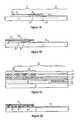
- FIGS. 1 (A)- 1 (D)An example of a display device according to the present invention is shown in FIGS. 1 (A)- 1 (D) in cross section.
- FIG. 1 (A)depicts the device with a relatively small magnification.
- the left side of this figureshows a driver circuit portion 7 having a semiconductor integrated circuit 2 .
- the right sideshows a matrix portion 8 .
- a conducting line pattern 4is formed from a transparent conductive film on a substrate 1 .
- a bump 6is made of gold or other similar material.
- the semiconductor integrated circuit 2has a thickness substantially equal to the thickness of TFTs.
- the integrated circuit 2has a connector portion having an electrode 5 made of a conductive oxide whose contact resistance is not varied if it is oxidized. The electrode 5 is brought into contact with the bump 6 .
- a resin 3is injected between the semiconductor integrated circuit 2 and the substrate 1 to mechanically hold the components (FIG. 1 (A)).
- FIG. 1 (B)is an enlarged view of the contact portion surrounded by the dotted line in FIG. 1 (A). It is to be noted that like components are indicated by like reference numerals in various figures.
- FIG. 1 (C)is an enlarged view of the portion surrounded by the dotted line in FIG. 1 (B).
- the semiconductor integrated circuitincludes an N-channel TFT 12 and a P-channel TFT 13 which are sandwiched by a buffer dielectric film 11 and an interlayer dielectric layer 14 and a passivation film 15 made of silicon nitride or the like (FIGS. 1 (B) and 1 (C)).
- the buffer film 11is normally made of silicon oxide. However, sufficient moisture resistance cannot be obtained only with this scheme. Therefore, a passivation film must be formed on the buffer film. If the semiconductor circuit and its contact portion are thinner than the spacing between the substrates of the device as shown in FIG. 3 , then it is possible to form a counter substrate 16 on the circuit. In this case, the outer side of the driver circuit portion 7 is sealed with a sealing material 17 such as epoxy resin, in the same way as the manufacture of a liquid crystal device as disclosed in Japanese Patent Laid-Open No. 66413/1993. The gap between the substrates 1 and 16 is filled with a liquid crystal material 18 and so mobile ions do not intrude into the gap from the outside. Hence, any special passivation film is not required (FIG. 3 ).
- the contact portioncan use a bump as described above. Another method is illustrated in FIG. 1 (D). That is, conductive particles 9 such as particles of gold are diffused into the contact portion to provide electrical contact. The diameter of the particles is slightly greater than the spacing between the semiconductor integrated circuit 2 and the substrate 1 (FIG. 1 (D)).
- FIGS. 2 (A)- 2 (G)The sequence for fabricating this display device which is of the passive matrix type is shown in FIGS. 2 (A)- 2 (G). First, a number of semiconductor integrated circuits 22 are formed on an appropriate substrate 21 (FIG. 2 (A)).
- the resulting laminateis cut to form stick crystals 23 and 24 .
- the electrical characteristics of the obtained stick crystals 23 and 24may be checked before the next manufacturing step is effected, to judge whether the crystals are acceptable or rejected (FIG. 2 (B)).
- the stick drivers 23 and 24are peeled from their respective substrates by SOI techniques or by processing with a gas containing a halogen. In this way, only semiconductor integrated circuits 29 and 30 are left on the surfaces 26 and 28 , respectively, of the substrates (FIGS. 2 (E) and 2 (F)).
- the row stick crystali.e., the stick crystal for a driver circuit for driving row lines
- the column stick crystali.e., the stick crystal for a driver circuit for driving column lines
- each substrateis made of a filmy material.
- FIGS. 1 (A)- 1 (D)are cross-sectional views of a display device according to the present invention.
- FIGS. 2 (A)- 2 (G)are exploded perspective views of another display device according to the invention, schematically illustrating a method of fabricating the device;
- FIG. 3is a cross-sectional view of a further display device according to the invention.
- FIGS. 4 (A)- 4 (C)are cross-sectional views of a stick crystal used for manufacturing steps according to the invention.
- FIGS. 5 (A)- 5 (D)are cross-sectional views, illustrating steps for bonding a stick crystal to a substrate.
- FIG. 6is a schematic view of a system for fabricating filmy liquid crystal devices in succession.
- Steps for forming a driver circuit on a stick crystalare schematically shown in FIGS. 4 (A)- 4 (C).
- Steps for mounting the stick crystal on the substrate of the liquid crystal displayare schematically shown in FIGS. 5 (A)- 5 (D).
- a silicon film having a thickness of 3000 ⁇was deposited as a peeling layer 32 on a glass substrate 31 . Since the silicon film becoming the peeling layer 32 is etched away when circuitry and a substrate formed on the silicon film are separated, the quality of the silicon film will present almost no problems. Therefore, the silicon film may be deposited by a method which permits mass production. Furthermore, the silicon film may be either amorphous or crystalline in character.
- the glass substratemay be made of Corning 7059 glass, Corning 1737 glass, NH Technoglass NA45, NH Technoglass NA35, Nippon Denki Glass OA2, other non-alkali or low-alkali glass, or quartz glass. Where quartz glass is used, the cost poses a problem. In the present invention, however, the area of the substrate used in one liquid crystal display is quite small and so the cost per device is sufficiently low.
- a silicon oxide filmwas deposited as a buffer film 33 having a thickness of 5000 ⁇ on the peeling layer 32 . Sufficient care must be taken in fabricating the buffer film 33 from silicon oxide. Islands 34 and 35 of crystalline silicon region were formed by a well-known method. The thickness of the islands of crystalline silicon region greatly affects the required semiconductor characteristics. Generally, it was desired to make the thickness smaller. In the present example, the thickness was 400-600 ⁇ .
- gate-insulating film 36 of silicon oxide having a thickness of 1200 ⁇was deposited by plasma CVD or thermal CVD.
- gate electrodes/interconnects 37 , 38were formed from a crystalline silicon film having a thickness of 5000 ⁇ .
- the gate electrodes/interconnects 37 , 38may be made from metals such as aluminum, tungsten, and titanium, or their silicides. Where metallic gate electrodes/interconnects 37 , 38 are formed, their top or side surfaces may be coated with anodic oxide as disclosed in Japanese Patent Laid-Open Nos. 267667/1993 and 338612/1994.
- the material of the gate electrodes/interconnects 37 , 38is determined according to the required semiconductor circuit characteristics, the maximum processing temperature of the substrate, and other factors (FIG. 4 (A)).
- N- and P-type impurity ionswere introduced into the islands of silicon 34 and 35 by self-aligned ion implantation or other method to form N-type regions 39 and P-type regions 40 .
- an interlayer dielectric film 41 of silicon oxide having a thickness of 5000 ⁇was deposited by a well-known means. Contact holes were created in this interlayer dielectric film.
- Aluminum alloy interconnects 41 - 44were formed (FIG. 4 (B)).
- a silicon nitride film 46 having a thickness of 2000 ⁇was deposited as a passivation film on the laminate by plasma CVD. Contact holes communicating with the output terminal lines 44 were formed in this passivation film.
- An ITO (indium-tin oxide) electrode 47 having a thickness of 1000 ⁇was formed by sputtering techniques. ITO is a transparent conductive oxide.
- a gold bump 48 having a diameter of about 50 ⁇ m and a height of 30 ⁇ mwas mechanically formed on the ITO electrode 47 . The resulting circuit was cut into appropriate size, thus obtaining a stick crystal (FIG. 4 (C)).
- An electrode 50was formed also from ITO to a thickness of 1000 ⁇ on another substrate 49 of the liquid crystal display.
- a substrate of polyethylene sulfite having a thickness of 0.3 mmwas used.
- the substrate 31 of the stick driverwas bonded to this substrate 49 under pressure.
- the electrodes 47 and 50were electrically connected to each other via the bump 48 (FIG. 5 (A)).
- an adhesive 51 to which a thermosetting organic resin was addedwas injected into the gap between the stick crystal 31 and the substrate 49 of the liquid crystal display.
- the adhesivemay be applied to the surface of any one of the stick crystal 31 and the substrate 49 before they are bonded together under pressure.
- the laminatewas processed for 15 minutes in an oven filled with a nitrogen ambient at 120° C. In this way, electrical connection and mechanical bonding between the stick crystal 31 and the substrate 49 were completed. Before the bonding operation is completed in this way, a check may be done to see whether the electrical connection is satisfactory or not by the method disclosed in the above-cited Japanese Patent Laid-Open No. 14880/1995 (FIG. 5 (B)).
- the laminate processed in this waywas allowed to stand in a stream of mixture gas of chlorine trifluoride (ClF 3 ) and nitrogen.
- the flow rate of each of the chlorine trifluoride and nitrogenwas 500 SCCM.
- the reaction pressurewas 1 to 10 torr.
- the temperaturewas room temperature. It is known that halogenated fluorine such as chlorine trifluoride selectively etches silicon. On the other hand, oxides such as silicon oxide and ITO are hardly etched. Also with respect to aluminum, if a stable oxide coating is formed on an aluminum film, then reaction no longer progresses. Hence, the aluminum is not etched.
- materials which might be attacked by chlorine trifluorideare the peeling layer (silicon) 32 , the islands of silicon 34 , 35 , the gate electrodes/interconnects 37 , 38 , the aluminum alloy interconnects 41 - 44 , and the adhesive 51 .
- These materials excluding the peeling layer 32 and the adhesive 51are capped with silicon oxide and other materials and, therefore, chlorine trifluoride is unable to reach them.
- only the peeling layer 32was selectively etched as shown in FIG. 5 (C), thus forming voids 52 .
- the present examplerelates to a method (referred to as the roll-to-roll method) of successively fabricating filmy passive matrix liquid crystal displays.
- a production system for implementing the present exampleis shown in FIG. 6 .
- the substrate material for obtaining the filmy liquid crystal displaysmay be selected from polyethylene sulfite, poly-carbonate, and polyimide. Since polyethylene terephthalate and polyethylene naphthalate are polycrystalline plastics, they are not appropriate as liquid crystal materials which provide displays making use of polarization of light.
- the production system shown in FIG. 6is divided into two major parts: the upper portion and the lower portion.
- a substrate on which color filters are formedis fabricated as a component of a liquid crystal display.
- a counter substrateis manufactured in the upper portion. First, steps for fabricating the substrate on which the color filters are formed are described.
- Color filters of the three primary colorsare printed on the surface of a film wound on a roll 71 .
- the color filtersare formed, using three sets of rolls 72 .
- this stepis dispensed with. This step is referred to as color filter printing.
- an overcoatis printed to form a planarization film, using rolls 73 .
- the overcoatacts to planarize the surface which is made uneven by the formation of the color filters.
- a transparent resinous materialmay be used as the material of the overcoat. This step is referred to as printing of overcoat (planarization film).
- row (column) electrodesare printed in a desired pattern, using a conductive ink, by means of rolls 74 . This step is referred to as formation of electrodes.
- orientation filmis printed, using rolls 75 .
- This stepis referred to as printing of orientation film.
- the filmis passed through a heating furnace 76 to bake and solidify the orientation film.
- This stepis referred to as the baking of orientation film.
- the filmis then passed between rolls 77 to rub the surface of the orientation film. In this way, the orientation step is completed. This step is referred to as rubbing.
- a stick crystalis mounted on the substrate by a pressure connection device 78 .
- This stepis referred to as mounting of the stick crystal.
- the laminateis passed through a heating furnace 79 to cure the adhesive.
- This stepis referred to as curing of the adhesive.
- the peeling layeruses silicon, in the same way as in Example 1. Then, the peeling layer is etched by a chlorine trifluoride chamber 80 which is differentially pumped to prevent the chlorine trifluoride from leaking out. As a result, the substrate is peeled from the stick crystal. This step is referred to as peeling of the stick crystal.
- spacersare sprayed onto the filmy substrate by a spacer applicator 81 .
- This stepis referred to as spraying of spacers.
- a sealing materialis printed, using rolls 82 .
- the sealing materialacts to bond together the two opposite substrates and to prevent the liquid crystal material from leaking from the space between the substrates.
- the semiconductor circuitis rendered thinner than the spacing between the substrates to seal the outer surface of the semiconductor integrated circuit as shown in FIG. 3 , as disclosed in the above-cited Japanese Patent Laid-Open No. 66413/1993.
- This stepis referred to as printing of the sealant.
- a liquid crystal materialis dripped, using a liquid crystal dripper 83 .
- a liquid crystal material layeris formed on the filmy substrate.
- the substrate on the side of the color filters, or a color filter panel,is completed.
- an orientation filmis formed by printing techniques, using rolls 63 .
- This stepis referred to as printing of the orientation film.
- the filmis passed through a heating furnace 64 to bake and solidify the orientation film. This step is referred to as baking of the orientation film.
- the filmy substrateis passed between rolls 65 to orient the molecules of the liquid crystal material. This step is referred to as rubbing.
- the stick crystalis mounted on the substrate by a pressure connection device 66 . This step is referred to mounting of the stick crystal.
- the laminateis passed through a heating furnace 67 to cure the adhesive. This step is referred to as curing of the adhesive.
- the substrate of the stick crystalis peeled off by a chlorine trifluoride chamber 68 .
- This stepis referred to as peeling of the stick crystal.
- the filmy substrate undergone the steps described thus faris passed around a roll 69 and sent to next rolls 84 .
- the substrate having the color filters and the counter substrateare bonded together by the rolls 84 , thus forming a liquid crystal cell. This step is referred to as bonding.
- the assemblyis then heated by a heating furnace 85 to cure the sealing material. In this way, the bonding of the substrates is completed. This step is referred to as curing of the sealant.
- the assemblyis cut into desired dimensions by a cutter 86 , thus completing a filmy liquid crystal display. This step is referred to as cutting.
- the kinds, the thickness, and the size of the substrates of the display devicecan be varied variously.
- a liquid crystal display in the form of a quite thin filmcan be obtained.
- the display devicemay be curved along a curved surface and bonded to it.
- less restrictionsare imposed on the kind of the substrates.
- a lightweight material having high shock resistancesuch as a plastic substrate may also be used. This improves the portability.
- the semiconductor integrated circuit forming a driver circuitis peeled from its support substrate by a halogen-containing gas which is not in a plasma state. Therefore, destruction of the semiconductor integrated circuit which would normally be caused by plasma damage can be prevented. This leads to an improvement in the yield with which liquid crystal displays are manufactured.
- the driver circuitoccupies less area and so the display device can be arranged relative to other devices with a greater degree of freedom.
- the driver circuitcan be confined within a region only a few centimeters wide around the display surface. Therefore, the display device itself is quite simple and is a highly fashionable industrial product. It can find extensive application. Hence, the present invention is industrially quite advantageous.
Landscapes
- Physics & Mathematics (AREA)
- Nonlinear Science (AREA)
- General Physics & Mathematics (AREA)
- Optics & Photonics (AREA)
- Crystallography & Structural Chemistry (AREA)
- Chemical & Material Sciences (AREA)
- Engineering & Computer Science (AREA)
- Mathematical Physics (AREA)
- Manufacturing & Machinery (AREA)
- Condensed Matter Physics & Semiconductors (AREA)
- Computer Hardware Design (AREA)
- Microelectronics & Electronic Packaging (AREA)
- Power Engineering (AREA)
- Liquid Crystal (AREA)
- Devices For Indicating Variable Information By Combining Individual Elements (AREA)
Abstract
Description
This is a continuation of U.S. application Ser. No. 09/062,873, filed Apr. 20, 1998, now U.S. Pat. No. 6,118,502, which is a continuation of U.S. application Ser. No. 08/611,336, filed Mar. 8, 1996, now U.S. Pat. No. 5,757,456, which claims priority from Japanese Patent applications 7-86457 filed Mar. 16, 1995 and 7-79708 filed Mar. 10, 1995.
1. Field of the Invention
The present invention relates to a passive matrix or active matrix display such as a liquid crystal display and, more particularly, to a fashionable display device in which the ratio of the area of the display portion to the area of the substrates of the display device is increased by effectively mounting a driver semiconductor integrated circuit.
2. Description of the Related Art
Passive matrix type and active matrix type constructions are known as matrix display devices. In the passive matrix type, a number of stripe-shaped conducting lines (row lines) made of a transparent conductive film or the like are arrayed in a certain direction on a first substrate. On a second substrate, similar stripe-shaped conducting lines (column lines) are arrayed in a direction substantially perpendicular to the conducting lines on the first substrate. Both substrates are so arranged that the conducting lines on them intersect each other.
An electrooptical material such as a liquid crystal material whose transparency, reflectivity, or scattering performance is varied by a voltage, current, or the like is positioned between both substrates. If a voltage or current is applied between an addressed row line on the first substrate and an addressed column line on the second substrate, then the transparency, reflectivity, or scattering performance at the intersection can be set to a desired value. In this way, the display device can be matrix driven.
In the active matrix construction, row and column lines are formed on the first substrate by multilayer metallization techniques. Pixel electrodes are formed at the intersections of the row and column lines. An active device such as a thin-film transistor (TFT) is formed at each pixel electrode to control the potential or current in the pixel electrode. A transparent conductive film is also formed on the second substrate. Both substrates are so arranged that the pixel electrodes on the first substrate are located opposite to the transparent conductive film on the second substrate.
In either type, the substrates are selected according to the used process. For example, the passive matrix construction needs no complex process steps except for steps where the transparent conductive films are formed and etched into row and column conducting line patterns. The substrates of this passive matrix type may be made from plastic, as well as from glass. On the other hand, to manufacture the active matrix construction, a relatively high-temperature film formation step is required. Furthermore, the active matrix type must keep out mobile ions such as sodium ions. The substrates of the active matrix type must be made of glass containing a quite low concentration of alkali.
In any type of prior art matrix display device excluding special constructions, a semiconductor integrated circuit (peripheral driver circuit) for driving the matrix is required to be mounted. In the past, this has been done by tape automated bonding (TAB) or chip on glass (COG). However, the matrix construction contains as many as several hundreds of rows. Therefore, the integrated circuit has a very large number of terminals. The corresponding driver circuit takes the form of a rectangular IC package or semiconductor chip. To connect these terminals with the conducting lines on the substrates, it is necessary to lay the conducting lines in a complex manner. As a consequence, the ratio of the area of the peripheral portion, or non-display portion, to the area of the display portion is not negligibly small.
A method for solving this problem is disclosed in Japanese Patent Laid-Open No. 14880/1995, and consisting of forming a driver circuit on an elongated substrate (referred to as a stick or stick crystal) having a length substantially equal to one side of the matrix construction and connecting the driver circuit with the terminal portion of the matrix. This arrangement is permitted, because a width of about 2 mm suffices for the driver circuit. Therefore, almost the whole area of the substrate can be made a viewing screen.
Of course, in this case, where the matrix has a large area, it is impossible to form a circuit on a silicon wafer. Consequently, it is necessary to form the circuit on a glass substrate or the like. Hence, active devices used in semiconductor devices are TFTs.
However, where a stick crystal is employed, the thickness of the substrate of the driver circuit has been an obstacle to miniaturization of the whole display device. For example, where the display device should be made thinner, the thickness of the substrate is allowed to be set to 0.3 mm by optimizing the kind of the substrate and the manufacturing steps. However, because of the strength necessary during manufacturing steps, it is difficult to reduce the thickness of the stick crystal below 0.5 mm. As a result, where two substrates are bonded together, the stick crystal protrudes as long as 0.2 mm or more.
Furthermore, if the stick crystal differs from the substrates of the display device in kind, then defects may be produced in the circuit because of the difference in coefficient of thermal expansion and for other causes. Especially, where a plastic substrate is used in a display device, this problem is conspicuous, because poor heat resistance of plastics makes it substantially impossible to use a plastic substrate as a stick crystal substrate.
Moreover, where the kind of the substrate supporting the stick crystal is different from the kind of the substrates of the display device, other known methods are used to circumvent the above-described problem. In one known method, a semiconductor integrated circuit having TFTs is fabricated on other support substrate. Then, the circuit is peeled off and adhesively bonded to another substrate. In another known method, the original support substrate is removed after adhesively bonding the circuit to another substrate. This technique is generally known as silicon-on-insulator (SOI) technique.
However, when the support substrate is removed, the semiconductor integrated circuit is often damaged, thus deteriorating the manufacturing yield.
It is an object of the present invention to provide a smaller display device of reduced weight by solving the foregoing problems with the stick crystal.
It is another object of the invention to provide a method of fabricating display devices with a high production yield by solving the aforementioned problems.
The present invention is characterized in that the driver circuit portion of a display device is made thinner by mechanically bonding a semiconductor integrated circuit equivalent to a stick crystal to a substrate for the display device, making electrical connections, and then removing only the substrate from the stick crystal. In this construction, stress induced by deformation caused by thermal expansion of the substrate is applied uniformly to the whole circuit. Therefore, the stress is prevented from being concentrated in certain portions; otherwise it would be inevitable that defects are produced.
Essentially, the present invention lies in a display device comprising a first substrate and a second substrate having a transparent conductive film on its surface. Conducting lines are formed on the first substrate. The first substrate has an elongated semiconductor integrated circuit which is electrically connected with the conducting lines and has TFTs. The transparent conductive film on the second substrate faces the surface of the first substrate on which the conducting lines are formed. The length of the semiconductor integrated circuit is roughly equal to the length of one side of the viewing surface, or the matrix, of the display device, in the same way as the stick crystal described in the above-cited Japanese Patent Laid-Open No. 14880/1995. The semiconductor integrated circuit is first fabricated on another substrate. The integrated circuit is peeled off and mounted on the first substrate.
In the case of the passive matrix type, the display device comprises a first substrate having an elongated first semiconductor circuit and a second substrate having a second semiconductor integrated circuit. A plurality of first conducting lines extending in a first direction are formed from a transparent conductive film on the first semiconductor integrated circuit. The first semiconductor integrated circuit is connected with the first conducting lines, has TFTs, and extends in a second direction substantially perpendicular to the first direction. The second substrate has second conducting lines which are formed from a transparent conductive film and extend in the second direction. The second semiconductor integrated circuit is connected with the second conducting lines, has TFTs, and extend in the first direction. The first and second substrates are so arranged that the first conducting lines are located opposite to the second conducting lines. The first and second semiconductor integrated circuits are obtained by fabricating them on other substrates, peeling the integrated circuits off, and bonding them to their respective substrates.
In the case of an active matrix type, the display device comprises a first substrate having a first and a second semiconductor integrated circuits and a second substrate having a transparent conductive film on its surface. A plurality of first conducting lines extending in a first direction are formed on the first substrate. The first semiconductor integrated circuit is connected with the first conducting lines, has TFTs, and extend in a second direction substantially perpendicular to the first direction. A plurality of second conducting lines extending in the second direction are formed also on the first substrate. The second semiconductor integrated circuit is connected with the second conducting lines, has TFTs, and extends in the first direction. The first and second substrates are so arranged that the first and second conducting lines on the first substrate are opposite to the transparent conductive film on the second substrate. The first and second semiconductor integrated circuits are obtained by fabricating them on other substrates, peeling the integrated circuits off, and mounting them to the first substrate.
The method consisting of forming a semiconductor integrated circuit having TFTs on other substrate, peeling off the circuit, and bonding the circuit to a further substrate (alternatively, the original substrate is removed after bonding to another substrate) is generally known as one of SOI (silicon-on-insulator) techniques and described in Japanese Patent Laid-Open No. 504139/1994. Also, other well-known techniques can be used.
The step for peeling a semiconductor integrated circuit from its support substrate needs the most advanced technique. The present invention is characterized in that when the semiconductor integrated circuit is peeled from the support substrate, a gas containing a halogen, especially halogen fluoride, is used.
A halogen fluoride is given by a chemical formula XFn, where X is a halogen other than fluorine and n is an integer. It is known that halogen fluorides include chlorine monofluoride (ClF), chlorine trifluoride (ClF3), bromine monofluoride (BrF), bromine trifluoride (BrF3), iodine monofluoride (IF), and iodine trifluoride (IF3).
A halogen fluoride is characterized in that it etches silicon even under a non-plasma state but does not etch silicon oxide at all. Since it is not necessary to use a plasma, the circuit is not destroyed by plasma damage. This effectively contributes to an improvement in the production yield. Furthermore, the etching selectivity between silicon oxide and silicon is quite high. This is advantageous in that neither the circuit nor the elements are destroyed.
In the present invention, a peeling layer consisting principally of silicon is formed on a support substrate. A semiconductor integrated circuit coated with silicon oxide is formed on the peeling layer. As mentioned above, silicon is etched by a halogen fluoride without using a plasma. Other gases containing a halogen such as carbon tetrafluoride (CF4) and nitrogen trifluoride (NF3) etch silicon under a plasma condition and so they can be used for the invention.
Accordingly, by placing the support substrate either within a gas containing a halogen such as a halogen fluoride or within a plasma, the peeling layer is peeled from the support substrate. As a consequence, the semiconductor integrated circuit can be peeled off.
An example of a display device according to the present invention is shown in FIGS.1(A)-1(D) in cross section. FIG.1(A) depicts the device with a relatively small magnification. The left side of this figure shows adriver circuit portion 7 having a semiconductor integratedcircuit 2. The right side shows amatrix portion 8. A conductingline pattern 4 is formed from a transparent conductive film on asubstrate 1. Abump 6 is made of gold or other similar material. The semiconductor integratedcircuit 2 has a thickness substantially equal to the thickness of TFTs. Theintegrated circuit 2 has a connector portion having anelectrode 5 made of a conductive oxide whose contact resistance is not varied if it is oxidized. Theelectrode 5 is brought into contact with thebump 6. Aresin 3 is injected between the semiconductor integratedcircuit 2 and thesubstrate 1 to mechanically hold the components (FIG.1(A)).
FIG.1(B) is an enlarged view of the contact portion surrounded by the dotted line in FIG.1(A). It is to be noted that like components are indicated by like reference numerals in various figures. FIG.1(C) is an enlarged view of the portion surrounded by the dotted line in FIG.1(B). The semiconductor integrated circuit includes an N-channel TFT 12 and a P-channel TFT 13 which are sandwiched by abuffer dielectric film 11 and aninterlayer dielectric layer 14 and apassivation film 15 made of silicon nitride or the like (FIGS.1(B) and1(C)).
When a semiconductor integrated circuit is formed, thebuffer film 11 is normally made of silicon oxide. However, sufficient moisture resistance cannot be obtained only with this scheme. Therefore, a passivation film must be formed on the buffer film. If the semiconductor circuit and its contact portion are thinner than the spacing between the substrates of the device as shown inFIG. 3 , then it is possible to form acounter substrate 16 on the circuit. In this case, the outer side of thedriver circuit portion 7 is sealed with a sealingmaterial 17 such as epoxy resin, in the same way as the manufacture of a liquid crystal device as disclosed in Japanese Patent Laid-Open No. 66413/1993. The gap between thesubstrates liquid crystal material 18 and so mobile ions do not intrude into the gap from the outside. Hence, any special passivation film is not required (FIG.3).
The contact portion can use a bump as described above. Another method is illustrated in FIG.1(D). That is,conductive particles 9 such as particles of gold are diffused into the contact portion to provide electrical contact. The diameter of the particles is slightly greater than the spacing between the semiconductor integratedcircuit 2 and the substrate1 (FIG.1(D)).
The sequence for fabricating this display device which is of the passive matrix type is shown in FIGS.2(A)-2(G). First, a number of semiconductor integratedcircuits 22 are formed on an appropriate substrate21 (FIG.2(A)).
The resulting laminate is cut to formstick crystals stick crystals
Then, the surfaces of thestick crystals surfaces separate substrates surfaces
Subsequently, thestick drivers circuits surfaces
Finally, the laminates obtained in this manner are made to face each other. As a result, a passive matrix display is derived. Asurface 26 faces away from thesurface 26. That is, no conducting line pattern is formed on the surface26 (FIG.2(G)).
In the above example, the row stick crystal (i.e., the stick crystal for a driver circuit for driving row lines) and the column stick crystal (i.e., the stick crystal for a driver circuit for driving column lines) are extracted from thesame substrate 21. Of course, they may be extracted from separate substrates.
The example shown in FIGS.2(A)-2(G) is a passive matrix display. Obviously, the invention can be similarly applied to an active matrix display. In the illustrated examples given below, each substrate is made of a filmy material.
Other objects and features of the invention will appear in the course of the description thereof, which follows.
FIGS.1(A)-1(D) are cross-sectional views of a display device according to the present invention;
FIGS.2(A)-2(G) are exploded perspective views of another display device according to the invention, schematically illustrating a method of fabricating the device;
FIGS.4(A)-4(C) are cross-sectional views of a stick crystal used for manufacturing steps according to the invention;
FIGS.5(A)-5(D) are cross-sectional views, illustrating steps for bonding a stick crystal to a substrate; and
Manufacturing steps for fabricating one substrate of a passive matrix liquid crystal display are briefly described now. The present example is described by referring to FIGS.4(A)-4(C) and5(A)-5(D). Steps for forming a driver circuit on a stick crystal are schematically shown in FIGS.4(A)-4(C). Steps for mounting the stick crystal on the substrate of the liquid crystal display are schematically shown in FIGS.5(A)-5(D).
First, a silicon film having a thickness of 3000 Å was deposited as a peeling layer32 on aglass substrate 31. Since the silicon film becoming the peeling layer32 is etched away when circuitry and a substrate formed on the silicon film are separated, the quality of the silicon film will present almost no problems. Therefore, the silicon film may be deposited by a method which permits mass production. Furthermore, the silicon film may be either amorphous or crystalline in character.
The glass substrate may be made of Corning 7059 glass, Corning 1737 glass, NH Technoglass NA45, NH Technoglass NA35, Nippon Denki Glass OA2, other non-alkali or low-alkali glass, or quartz glass. Where quartz glass is used, the cost poses a problem. In the present invention, however, the area of the substrate used in one liquid crystal display is quite small and so the cost per device is sufficiently low.
A silicon oxide film was deposited as a buffer film33 having a thickness of 5000 Å on the peeling layer32. Sufficient care must be taken in fabricating the buffer film33 from silicon oxide.Islands
Where crystalline silicon is obtained, laser annealing (i.e., amorphous silicon is illuminated with intense light such as laser light) or solid-phase epitaxy using thermal annealing is employed. Where solid-phase epitaxy is utilized, if a catalytic element such as nickel is added to the silicon as disclosed in Japanese Patent Laid-Open No. 244104/1994, then the crystallization temperature can be lowered, and the annealing time can be shortened. Furthermore, as described in Japanese Patent Laid-Open No. 318701/1994, once silicon is crystallized by solid-phase epitaxy, it may be laser-annealed. The adopted method is determined, taking account of the required semiconductor circuit characteristics, the maximum processing temperature of the substrate, and other factors. Then, a gate-insulatingfilm 36 of silicon oxide having a thickness of 1200 Å was deposited by plasma CVD or thermal CVD. Subsequently, gate electrodes/interconnects37,38 were formed from a crystalline silicon film having a thickness of 5000 Å. The gate electrodes/interconnects37,38 may be made from metals such as aluminum, tungsten, and titanium, or their silicides. Where metallic gate electrodes/interconnects37,38 are formed, their top or side surfaces may be coated with anodic oxide as disclosed in Japanese Patent Laid-Open Nos. 267667/1993 and 338612/1994. The material of the gate electrodes/interconnects37,38 is determined according to the required semiconductor circuit characteristics, the maximum processing temperature of the substrate, and other factors (FIG.4(A)).
Thereafter, N- and P-type impurity ions were introduced into the islands ofsilicon type regions 39 and P-type regions40. Then, aninterlayer dielectric film 41 of silicon oxide having a thickness of 5000 Å was deposited by a well-known means. Contact holes were created in this interlayer dielectric film. Aluminum alloy interconnects41-44 were formed (FIG.4(B)).
Asilicon nitride film 46 having a thickness of 2000 Å was deposited as a passivation film on the laminate by plasma CVD. Contact holes communicating with theoutput terminal lines 44 were formed in this passivation film. An ITO (indium-tin oxide)electrode 47 having a thickness of 1000 Å was formed by sputtering techniques. ITO is a transparent conductive oxide. Agold bump 48 having a diameter of about 50 μm and a height of 30 μm was mechanically formed on theITO electrode 47. The resulting circuit was cut into appropriate size, thus obtaining a stick crystal (FIG.4(C)).
Anelectrode 50 was formed also from ITO to a thickness of 1000 Å on anothersubstrate 49 of the liquid crystal display. In the present example, a substrate of polyethylene sulfite having a thickness of 0.3 mm was used. Thesubstrate 31 of the stick driver was bonded to thissubstrate 49 under pressure. At this time, theelectrodes
Then, an adhesive51 to which a thermosetting organic resin was added was injected into the gap between thestick crystal 31 and thesubstrate 49 of the liquid crystal display. The adhesive may be applied to the surface of any one of thestick crystal 31 and thesubstrate 49 before they are bonded together under pressure.
The laminate was processed for 15 minutes in an oven filled with a nitrogen ambient at 120° C. In this way, electrical connection and mechanical bonding between thestick crystal 31 and thesubstrate 49 were completed. Before the bonding operation is completed in this way, a check may be done to see whether the electrical connection is satisfactory or not by the method disclosed in the above-cited Japanese Patent Laid-Open No. 14880/1995 (FIG.5(B)).
The laminate processed in this way was allowed to stand in a stream of mixture gas of chlorine trifluoride (ClF3) and nitrogen. The flow rate of each of the chlorine trifluoride and nitrogen was 500 SCCM. The reaction pressure was 1 to 10 torr. The temperature was room temperature. It is known that halogenated fluorine such as chlorine trifluoride selectively etches silicon. On the other hand, oxides such as silicon oxide and ITO are hardly etched. Also with respect to aluminum, if a stable oxide coating is formed on an aluminum film, then reaction no longer progresses. Hence, the aluminum is not etched.
In the present example, materials which might be attacked by chlorine trifluoride are the peeling layer (silicon)32, the islands ofsilicon
As time passed further, the peeling layer32 was completely etched away, so that thebottom surface 53 of the buffer film33 was exposed. Thus, thesubstrate 31 of the stick crystal was separated from the semiconductor circuit. With etching using chlorine trifluoride, the etching process came to a stop at the bottom surface of the buffer film and so thebottom surface 53 was quite flat (FIG.5(D)).
In this manner, fabrication of the semiconductor integrated circuit on one substrate of the liquid crystal display was completed. The liquid crystal display is completed, using the substrate obtained in this way.
The present example relates to a method (referred to as the roll-to-roll method) of successively fabricating filmy passive matrix liquid crystal displays. A production system for implementing the present example is shown in FIG.6. The substrate material for obtaining the filmy liquid crystal displays may be selected from polyethylene sulfite, poly-carbonate, and polyimide. Since polyethylene terephthalate and polyethylene naphthalate are polycrystalline plastics, they are not appropriate as liquid crystal materials which provide displays making use of polarization of light.
The production system shown inFIG. 6 is divided into two major parts: the upper portion and the lower portion. In the lower portion, a substrate on which color filters are formed is fabricated as a component of a liquid crystal display. In the upper portion, a counter substrate is manufactured. First, steps for fabricating the substrate on which the color filters are formed are described.
Color filters of the three primary colors (RGB) are printed on the surface of a film wound on aroll 71. The color filters are formed, using three sets ofrolls 72. Where the manufactured liquid crystal displays are monochrome devices, this step is dispensed with. This step is referred to as color filter printing.
Then, an overcoat is printed to form a planarization film, using rolls73. The overcoat acts to planarize the surface which is made uneven by the formation of the color filters. A transparent resinous material may be used as the material of the overcoat. This step is referred to as printing of overcoat (planarization film).
Then, row (column) electrodes are printed in a desired pattern, using a conductive ink, by means ofrolls 74. This step is referred to as formation of electrodes.
Thereafter, an orientation film is printed, using rolls75. This step is referred to as printing of orientation film. The film is passed through aheating furnace 76 to bake and solidify the orientation film. This step is referred to as the baking of orientation film.
The film is then passed betweenrolls 77 to rub the surface of the orientation film. In this way, the orientation step is completed. This step is referred to as rubbing.
Then, a stick crystal is mounted on the substrate by apressure connection device 78. This step is referred to as mounting of the stick crystal. The laminate is passed through aheating furnace 79 to cure the adhesive. Thus, the bonding operation is completed. This step is referred to as curing of the adhesive.
In the present example, the peeling layer uses silicon, in the same way as in Example 1. Then, the peeling layer is etched by achlorine trifluoride chamber 80 which is differentially pumped to prevent the chlorine trifluoride from leaking out. As a result, the substrate is peeled from the stick crystal. This step is referred to as peeling of the stick crystal.
Then, spacers are sprayed onto the filmy substrate by aspacer applicator 81. This step is referred to as spraying of spacers. A sealing material is printed, using rolls82. The sealing material acts to bond together the two opposite substrates and to prevent the liquid crystal material from leaking from the space between the substrates. In the present example, the semiconductor circuit is rendered thinner than the spacing between the substrates to seal the outer surface of the semiconductor integrated circuit as shown inFIG. 3 , as disclosed in the above-cited Japanese Patent Laid-Open No. 66413/1993. This step is referred to as printing of the sealant.
Subsequently, a liquid crystal material is dripped, using aliquid crystal dripper 83. As a result, a liquid crystal material layer is formed on the filmy substrate. In this way, the substrate on the side of the color filters, or a color filter panel, is completed. These manufacturing steps are made to progress successively by rotating the various rolls.
Then, steps for manufacturing the counter substrate are described. Column (row) electrodes are formed in a desired pattern on the filmy substrate fed out of aroll 61 by means ofrolls 62. This step is referred to as formation of electrodes.
Thereafter, an orientation film is formed by printing techniques, using rolls63. This step is referred to as printing of the orientation film. The film is passed through aheating furnace 64 to bake and solidify the orientation film. This step is referred to as baking of the orientation film.
Then, the filmy substrate is passed betweenrolls 65 to orient the molecules of the liquid crystal material. This step is referred to as rubbing.
The stick crystal is mounted on the substrate by apressure connection device 66. This step is referred to mounting of the stick crystal. The laminate is passed through aheating furnace 67 to cure the adhesive. This step is referred to as curing of the adhesive.
Then, the substrate of the stick crystal is peeled off by achlorine trifluoride chamber 68. This step is referred to as peeling of the stick crystal.
The filmy substrate undergone the steps described thus far is passed around aroll 69 and sent to next rolls84. The substrate having the color filters and the counter substrate are bonded together by therolls 84, thus forming a liquid crystal cell. This step is referred to as bonding.
The assembly is then heated by aheating furnace 85 to cure the sealing material. In this way, the bonding of the substrates is completed. This step is referred to as curing of the sealant.
The assembly is cut into desired dimensions by acutter 86, thus completing a filmy liquid crystal display. This step is referred to as cutting.
In the present invention, the kinds, the thickness, and the size of the substrates of the display device can be varied variously. For example, as described in Example 2, a liquid crystal display in the form of a quite thin film can be obtained. In this case, the display device may be curved along a curved surface and bonded to it. Furthermore, less restrictions are imposed on the kind of the substrates. As a consequence, a lightweight material having high shock resistance such as a plastic substrate may also be used. This improves the portability.
In addition, in the present invention, the semiconductor integrated circuit forming a driver circuit is peeled from its support substrate by a halogen-containing gas which is not in a plasma state. Therefore, destruction of the semiconductor integrated circuit which would normally be caused by plasma damage can be prevented. This leads to an improvement in the yield with which liquid crystal displays are manufactured.
Moreover, the driver circuit occupies less area and so the display device can be arranged relative to other devices with a greater degree of freedom. Typically, the driver circuit can be confined within a region only a few centimeters wide around the display surface. Therefore, the display device itself is quite simple and is a highly fashionable industrial product. It can find extensive application. Hence, the present invention is industrially quite advantageous.
Claims (27)
1. A method of manufacturing an active matrix display device wherein said display device has a first substrate provided with a plurality of pixel electrodes and switching thin film transistors for switching said pixel electrodes, and a first electrode comprising a transparent conductive oxide, the method comprising the steps of:
forming a semiconductor film over a glass substrate;
crystallizing said semiconductor film;
patterning the crystallized semiconductor film into a plurality of semiconductor islands;
forming a plurality of thin film transistors using said semiconductor islands;
forming a driver circuit with said plurality of thin film transistors;
forming a passivation film over said driver circuit;
forming a second electrode comprising a transparent conductive oxide over said passivation film, said second electrode electrically connected to said driver circuit through a contact hole of said passivation film;
attaching said glass substrate provided with said driver circuit to said first substrate so that said second electrode is electrically connected to said first electrode.
2. A method of manufacturing a display device comprising:
preparing at least one display substrate provided with first electrodes comprising a transparent conductive oxide;
forming a semiconductor film over a glass substrate;
crystallizing said semiconductor film formed over said glass substrate;
patterning the crystallized semiconductor film into a plurality of semiconductor islands;
forming a plurality of thin film transistors with said semiconductor islands for constituting a plurality of driver circuits;
forming a passivation film over said plurality of thin film transistors;
forming second electrodes comprising a transparent conductive oxide over said passivation film, said second electrodes electrically connected to said driver circuits through contact holes of said passivation film;
dividing said glass substrate to obtain at least one divided glass substrate wherein said divided glass substrate carries at least one of said driver circuits and at least one of said second electrodes thereon; and
attaching said divided glass substrate to a display substrate so that said at least one of the second electrodes is electrically connected to said first electrodes.
3. A method according toclaim 2 wherein said display device is a passive type liquid crystal device.
4. A method according toclaim 2 wherein said display device is an active matrix type liquid crystal device.
5. A method according toclaim 2 further comprising a step of removing the divided glass substrate from said display substrate.
6. A method of manufacturing a display device comprising:
preparing at least one display substrate provided with first electrodes wherein said display substrate comprises a plastic;
forming a semiconductor film over a glass substrate;
crystallizing said semiconductor film formed over said display substrate;
patterning the crystallized semiconductor film into a plurality of semiconductor islands;
forming a plurality of thin film transistors with said semiconductor islands as an active layer thereof for constituting a plurality of driver circuits;
forming a passivation film over said plurality of thin film transistors;
forming second electrodes over said passivation film, said second electrodes electrically connected to said driver circuits through contact holes of said passivation film;
dividing said glass substrate to obtain at least one divided glass substrate wherein said divided glass substrate carries at least one of said driver circuits thereon and at least one of said second electrodes; and
attaching said divided glass substrate to a display substrate so that said at least one of the second electrodes is electrically connected to said first electrodes,
wherein both of said first and second electrodes comprise a transparent conductive oxide.
7. A method according toclaim 6 wherein said display device is a passive type liquid crystal device.
8. A method according toclaim 6 further comprising a step of removing the divided glass substrate from said display substrate.
9. A method of manufacturing an active matrix type display device comprising:
preparing at least one display substrate provided with a plurality of pixel electrodes and switching thin film transistors for switching said pixel electrodes and first electrodes for supplying signals to said switching thin film transistors;
forming a semiconductor film over a glass substrate;
crystallizing said semiconductor film;
patterning the crystallized semiconductor film into a plurality of semiconductor islands;
forming a plurality of thin film transistors with said semiconductor islands as an active layer thereof for constituting a plurality of driver circuits;
forming a passivation film over said plurality of thin film transistors;
forming second electrodes over said passivation film, said second electrodes electrically connected to said driver circuits through contact holes of said passivation film;
dividing said glass substrate to obtain at least one divided glass substrate wherein said divided glass substrate carries at least one of said driver circuits thereon and at least one of said second electrodes; and
attaching said divided glass substrate to a display substrate so that said at least one of the second electrodes is electrically connected to at least one of said first electrodes,
wherein both of said first and second electrodes comprise a transparent conductive oxide.
10. A method according toclaim 9 further comprising a step of removing the divided glass substrate from said display substrate.
11. A method according toclaim 9 wherein a thickness of said semiconductor islands is from 400 to 600 Å.
12. A method of manufacturing an active matrix type display device comprising:
preparing at least one display substrate provided with a plurality of pixel electrodes and switching thin film transistors for switching said pixel electrodes and first electrodes for supplying signals to said thin film transistors;
forming a semiconductor film over a glass substrate;
crystallizing said semiconductor film wherein the crystallization is promoted by adding a catalyst to said semiconductor film;
patterning the crystallized semiconductor film into a plurality of semiconductor islands;
forming a plurality of thin film transistors with said semiconductor islands as an active layer thereof for constituting a plurality of driver circuits;
forming a passivation film over said plurality of thin film transistors;
forming second electrodes over said passivation film, said second electrodes electrically connected to said driver circuits through contact holes of said passivation film;
dividing said glass substrate to obtain at least one divided glass substrate wherein said divided glass substrate carries at least one of said driver circuits thereon and at least one of said second electrodes; and
attaching said divided glass substrate to a display substrate so that said at least one of the second electrodes is electrically connected to said first electrodes,
wherein both of said first and second electrodes comprise a transparent conductive oxide.
13. A method according toclaim 12 further comprising a step of removing the divided glass substrate from said display substrate.
14. A method according toclaim 12 wherein a thickness of said semiconductor islands is from 400 to 600 Å.
15. A method according toclaim 12 wherein said catalyst comprises nickel.
16. A method of manufacturing a display device comprising:
preparing at least one display substrate provided with a plurality of first electrodes comprising a transparent oxide;
forming a semiconductor film over a glass substrate;
crystallizing said semiconductor film;
patterning the crystallized semiconductor film into a plurality of semiconductor islands;
forming a plurality of thin film transistors with said semiconductor islands as an active layer thereof for constituting a plurality of driver circuits;
forming a passivation film over the plurality of thin film transistors;
forming transparent electrodes over said passivation film wherein said transparent electrodes comprise a transparent conductive oxide;
forming metal bumps on said transparent electrodes;
dividing said glass substrate to obtain at least one divided glass substrate wherein said divided glass substrate carries at least one of said driver circuits thereon; and
attaching said divided glass substrate to a display substrate so that said driver circuit is electrically connected to said first electrodes through said transparent electrodes and said metal bumps.
17. A method according toclaim 16 further comprising a step of removing the divided glass substrate from said display substrate.
18. A method according toclaim 16 wherein a thickness of said semiconductor islands is from 400 to 600 Å.
19. A method according toclaim 16 wherein said passivation film comprises silicon nitride.
20. A method according toclaim 16 wherein said display device is a passive type liquid crystal device.
21. A method according toclaim 16 wherein said display device is an active matrix type liquid crystal device.
22. A method of manufacturing a display device comprising:
preparing at least one display substrate provided with a plurality of first transparent electrodes;
forming a semiconductor film over a glass substrate;
crystallizing said semiconductor film;
patterning the crystallized semiconductor film into a plurality of semiconductor islands;
forming a plurality of thin film transistors with said semiconductor islands as an active layer thereof for constituting a plurality of driver circuits;
forming a passivation film over the plurality of thin film transistors;
forming second transparent electrodes over said passivation film wherein said transparent electrodes comprise a transparent conductive oxide;
dividing said glass substrate to obtain at least one divided glass substrate wherein said divided glass substrate carries at least one of said driver circuits thereon; and
attaching said divided glass substrate to a display substrate so that said driver circuit is electrically connected to said electrodes through said first and second transparent electrodes.
23. A method according toclaim 22 wherein a thickness of said semiconductor islands is from 400 to 600 Å.
24. A method according toclaim 22 wherein said display device is a passive type liquid crystal device.
25. A method according toclaim 22 further comprising a step of removing the divided glass substrate from said display substrate so that said driver circuit remains connected to said electrodes.
26. A method according toclaim 22 wherein said display device is a passive type liquid crystal device.
27. A method according toclaim 22 wherein said display device is an active matrix type liquid crystal device.
Priority Applications (6)
| Application Number | Priority Date | Filing Date | Title |
|---|---|---|---|
| US09/517,354US7050138B1 (en) | 1995-03-10 | 2000-03-02 | Method of manufacturing a display device having a driver circuit attached to a display substrate |
| US10/300,226US20030071953A1 (en) | 1995-03-10 | 2002-11-19 | Display device and method of fabricating the same |
| US10/968,953US20050070038A1 (en) | 1995-03-10 | 2004-10-21 | Display device and method of fabricating the same |
| US11/776,683US7446843B2 (en) | 1995-03-10 | 2007-07-12 | Display device and method of fabricating the same |
| US12/264,641US8013972B2 (en) | 1995-03-10 | 2008-11-04 | Display device and method of fabricating the same |
| US13/224,395US8547516B2 (en) | 1995-03-10 | 2011-09-02 | Display device and method of fabricating the same |
Applications Claiming Priority (5)
| Application Number | Priority Date | Filing Date | Title |
|---|---|---|---|
| JP07970895AJP3406727B2 (en) | 1995-03-10 | 1995-03-10 | Display device |
| JP8645795AJP3579492B2 (en) | 1995-03-16 | 1995-03-16 | Method for manufacturing display device |
| US08/611,336US5757456A (en) | 1995-03-10 | 1996-03-08 | Display device and method of fabricating involving peeling circuits from one substrate and mounting on other |
| US09/062,873US6118502A (en) | 1995-03-10 | 1998-04-20 | Using a temporary substrate to attach components to a display substrate when fabricating a passive type display device |
| US09/517,354US7050138B1 (en) | 1995-03-10 | 2000-03-02 | Method of manufacturing a display device having a driver circuit attached to a display substrate |
Related Parent Applications (1)
| Application Number | Title | Priority Date | Filing Date |
|---|---|---|---|
| US09/062,873ContinuationUS6118502A (en) | 1995-03-10 | 1998-04-20 | Using a temporary substrate to attach components to a display substrate when fabricating a passive type display device |
Related Child Applications (2)
| Application Number | Title | Priority Date | Filing Date |
|---|---|---|---|
| US10/300,226ContinuationUS20030071953A1 (en) | 1995-03-10 | 2002-11-19 | Display device and method of fabricating the same |
| US11/776,683ContinuationUS7446843B2 (en) | 1995-03-10 | 2007-07-12 | Display device and method of fabricating the same |
Publications (1)
| Publication Number | Publication Date |
|---|---|
| US7050138B1true US7050138B1 (en) | 2006-05-23 |
Family
ID=26420707
Family Applications (8)
| Application Number | Title | Priority Date | Filing Date |
|---|---|---|---|
| US08/611,336Expired - LifetimeUS5757456A (en) | 1995-03-10 | 1996-03-08 | Display device and method of fabricating involving peeling circuits from one substrate and mounting on other |
| US09/062,873Expired - LifetimeUS6118502A (en) | 1995-03-10 | 1998-04-20 | Using a temporary substrate to attach components to a display substrate when fabricating a passive type display device |
| US09/517,354Expired - Fee RelatedUS7050138B1 (en) | 1995-03-10 | 2000-03-02 | Method of manufacturing a display device having a driver circuit attached to a display substrate |
| US10/300,226AbandonedUS20030071953A1 (en) | 1995-03-10 | 2002-11-19 | Display device and method of fabricating the same |
| US10/968,953AbandonedUS20050070038A1 (en) | 1995-03-10 | 2004-10-21 | Display device and method of fabricating the same |
| US11/776,683Expired - Fee RelatedUS7446843B2 (en) | 1995-03-10 | 2007-07-12 | Display device and method of fabricating the same |
| US12/264,641Expired - Fee RelatedUS8013972B2 (en) | 1995-03-10 | 2008-11-04 | Display device and method of fabricating the same |
| US13/224,395Expired - Fee RelatedUS8547516B2 (en) | 1995-03-10 | 2011-09-02 | Display device and method of fabricating the same |
Family Applications Before (2)
| Application Number | Title | Priority Date | Filing Date |
|---|---|---|---|
| US08/611,336Expired - LifetimeUS5757456A (en) | 1995-03-10 | 1996-03-08 | Display device and method of fabricating involving peeling circuits from one substrate and mounting on other |
| US09/062,873Expired - LifetimeUS6118502A (en) | 1995-03-10 | 1998-04-20 | Using a temporary substrate to attach components to a display substrate when fabricating a passive type display device |
Family Applications After (5)
| Application Number | Title | Priority Date | Filing Date |
|---|---|---|---|
| US10/300,226AbandonedUS20030071953A1 (en) | 1995-03-10 | 2002-11-19 | Display device and method of fabricating the same |
| US10/968,953AbandonedUS20050070038A1 (en) | 1995-03-10 | 2004-10-21 | Display device and method of fabricating the same |
| US11/776,683Expired - Fee RelatedUS7446843B2 (en) | 1995-03-10 | 2007-07-12 | Display device and method of fabricating the same |
| US12/264,641Expired - Fee RelatedUS8013972B2 (en) | 1995-03-10 | 2008-11-04 | Display device and method of fabricating the same |
| US13/224,395Expired - Fee RelatedUS8547516B2 (en) | 1995-03-10 | 2011-09-02 | Display device and method of fabricating the same |
Country Status (1)
| Country | Link |
|---|---|
| US (8) | US5757456A (en) |
Cited By (55)
| Publication number | Priority date | Publication date | Assignee | Title |
|---|---|---|---|---|
| US20030032210A1 (en)* | 2001-07-16 | 2003-02-13 | Semiconductor Energy Laboratory Co., Ltd. | Semiconductor device and peeling off method and method of manufacturing semiconductor device |
| US20040124542A1 (en)* | 2002-12-26 | 2004-07-01 | Hideaki Kuwabara | Semiconductor device and method for manufacturing the same |
| US20040212012A1 (en)* | 2003-01-22 | 2004-10-28 | Shunpei Yamazaki | Semiconductor device |
| US20040238827A1 (en)* | 2003-03-14 | 2004-12-02 | Toru Takayama | Semiconductor device and method for manufacturing the same |
| US20050082463A1 (en)* | 2003-09-19 | 2005-04-21 | Jun Koyama | Optical sensor device and electronic apparatus |
| US20050167573A1 (en)* | 2003-10-06 | 2005-08-04 | Junya Maruyama | Semiconductor device and manufacturing method thereof |
| US20050253178A1 (en)* | 2004-04-23 | 2005-11-17 | Semiconductor Energy Laboratory Co., Ltd. | Thin film integrated circuit and method for manufacturing the same, CPU, memory, electronic card and electronic device |
| US20050280037A1 (en)* | 2002-03-29 | 2005-12-22 | Seiko Epson Corporation | Semiconductor, electrooptic apparatus and electronic apparatus |
| US20060110863A1 (en)* | 2004-11-22 | 2006-05-25 | Yoshiaki Yamamoto | Semiconductor device, and method for manufacturing the same |
| US20060146266A1 (en)* | 1996-04-12 | 2006-07-06 | Semiconductor Energy Laboratory Co., Ltd. | Liquid crystal display device and method for fabricating thereof |
| US20060163710A1 (en)* | 2002-12-27 | 2006-07-27 | Semiconductor Energy Laboratory Co., Ltd. | Semiconductor device and manufacturing method thereof |
| US20070028444A1 (en)* | 2002-04-25 | 2007-02-08 | Seiko Epson Corporation | Method of manufacturing electronic device including aligning first substrate, second substrate and mask, and transferring object from first substrate to second substrate, including irradiating object on first substrate with light through mask |
| US20070115416A1 (en)* | 1997-11-28 | 2007-05-24 | Semiconductor Energy Laboratory Co., Ltd. | Liquid Crystal Electrooptical Device |
| US20070159547A1 (en)* | 2006-01-10 | 2007-07-12 | Fujifilm Corporation | Solid state image pickup device |
| US20070181246A1 (en)* | 2003-11-28 | 2007-08-09 | Semiconductor Energy Laboratory Co., Ltd. | Method of manufacturing display device |
| US20070212875A1 (en)* | 2004-06-24 | 2007-09-13 | Semiconductor Energy Laboratory Co., Ltd. | Method for manufacturing thin film integrated circuit |
| US20080042168A1 (en)* | 2004-07-30 | 2008-02-21 | Semiconductor Energy Laboratory Co., Ltd. | Laminating System, Ic Sheet, Scroll of Ic Sheet, and Method for Manufacturing Ic Chip |
| US20080044940A1 (en)* | 2004-06-02 | 2008-02-21 | Ryosuke Watanabe | Laminating System |
| US20080303140A1 (en)* | 2007-06-07 | 2008-12-11 | Semiconductor Energy Laboratory Co., Ltd. | Semiconductor device |
| US20090042387A1 (en)* | 2005-05-20 | 2009-02-12 | Semiconductor Energy Laboratory Co., Ltd. | Manufacturing method of semiconductor device |
| US20090061721A1 (en)* | 2007-08-30 | 2009-03-05 | Semiconductor Energy Laboratory Co., Ltd. | Method for manufacturing semiconductor device |
| US20090085182A1 (en)* | 2007-07-27 | 2009-04-02 | Shunpei Yamazaki | Semiconductor device and method for manufacturing the same |
| US20090090940A1 (en)* | 2005-05-31 | 2009-04-09 | Semiconductor Energy Laboratory Co., Ltd. | Semiconductor device |
| US20090166896A1 (en)* | 2007-12-28 | 2009-07-02 | Shunpei Yamazaki | Semiconductor device and method of manufacturing semiconductor device |
| US20090174023A1 (en)* | 2007-12-28 | 2009-07-09 | Hidekazu Takahashi | Semiconductor device and method of manufacturing semiconductor device |
| US20090183766A1 (en)* | 2008-01-22 | 2009-07-23 | Hidekazu Takahashi | Semiconductor device and method of manufacturing semiconductor device |
| US20090194154A1 (en)* | 2008-02-01 | 2009-08-06 | Semiconductor Energy Laboratory Co., Ltd. | Semiconductor device and method of manufacturing semiconductor device |
| US7591863B2 (en) | 2004-07-16 | 2009-09-22 | Semiconductor Energy Laboratory Co., Ltd. | Laminating system, IC sheet, roll of IC sheet, and method for manufacturing IC chip |
| US20090267173A1 (en)* | 2008-03-27 | 2009-10-29 | Hidekazu Takahashi | Semiconductor device and method for manufacturing semiconductor device |
| US20090267225A1 (en)* | 2008-04-25 | 2009-10-29 | Shingo Eguchi | Semiconductor device and method for manufacturing the same |
| US20090278252A1 (en)* | 2008-05-12 | 2009-11-12 | Semiconductor Energy Laboratory Co., Ltd. | Semiconductor device and method for manufacturing semiconductor device |
| US20090291516A1 (en)* | 2001-08-22 | 2009-11-26 | Semiconductor Energy Laboratory Co., Ltd. | Peeling Method and Method of Manufacturing Semiconductor Device |
| US20090289340A1 (en)* | 2008-05-23 | 2009-11-26 | Semiconductor Energy Laboratory Co., Ltd | Semiconductor device and method for manufacturing the same |
| US20090289341A1 (en)* | 2008-05-23 | 2009-11-26 | Semiconductor Energy Laboratory Co., Ltd. | Semiconductor device |
| US20090305467A1 (en)* | 2008-06-06 | 2009-12-10 | Semiconductor Energy Laboratory Co., Ltd. | Method for manufacturing semiconductor device |
| US20090302455A1 (en)* | 2008-06-06 | 2009-12-10 | Semiconductor Energy Laboratory Co., Ltd. | Semiconductor device and method for manufacturing the same |
| US20100007829A1 (en)* | 2008-07-10 | 2010-01-14 | Yoshiaki Oikawa | Liquid crystal display device and method for manufacturing the same |
| US20100006746A1 (en)* | 2008-07-10 | 2010-01-14 | Semiconductor Energy Laboratory Co., Ltd. | Color sensor and electronic device having the same |
| US20100013372A1 (en)* | 2008-07-10 | 2010-01-21 | Yoshiaki Oikawa | Light Emitting Device and Electronic Device |
| US20100039602A1 (en)* | 1993-12-03 | 2010-02-18 | Semiconductor Energy Laboratory Co., Ltd. | Electro-optical device and method for manufacturing the same |
| US20100065952A1 (en)* | 2008-09-18 | 2010-03-18 | Semiconductor Energy Laboratory Co., Ltd. | Semiconductor Device |
| US20100072548A1 (en)* | 2008-09-19 | 2010-03-25 | Semiconductor Energy Laboratory Co., Ltd. | Semiconductor Device and Method for Manufacturing the Same |
| US20100078787A1 (en)* | 2008-10-01 | 2010-04-01 | Semiconductor Energy Laboratory Co., Ltd. | Semiconductor device |
| US7759788B2 (en) | 2007-08-30 | 2010-07-20 | Semiconductor Energy Laboratory Co., Ltd | Semiconductor device |
| US20100193788A1 (en)* | 2000-08-10 | 2010-08-05 | Semiconductor Energy Laboratory Co., Ltd. | Area sensor and display apparatus provided with an area sensor |
| US20100311212A1 (en)* | 1995-03-18 | 2010-12-09 | Semiconductor Energy Laboratory Co., Ltd. | Method for producing display device |
| US7888714B2 (en) | 2004-10-04 | 2011-02-15 | Semiconductor Energy Laboratory Co., Ltd. | Semiconductor device and method of manufacturing the same |
| US8284369B2 (en) | 2008-08-20 | 2012-10-09 | Semiconductor Energy Laboratory Co., Ltd. | Flexible light-emitting device, and method for fabricating the same |
| US8344369B2 (en) | 2001-12-28 | 2013-01-01 | Semiconductor Energy Laboratory Co., Ltd. | Vehicle that includes a display panel having a curved surface |
| US8878275B2 (en)* | 2013-02-18 | 2014-11-04 | Fairchild Semiconductor Corporation | LDMOS device with double-sloped field plate |
| US8981641B2 (en) | 2003-10-28 | 2015-03-17 | Semiconductor Energy Laboratory Co., Ltd. | Method of manufacturing optical film |
| US9419355B2 (en) | 2012-12-07 | 2016-08-16 | Samsung Electronics Co., Ltd. | Display module with dual power lines |
| US9947568B2 (en) | 2013-02-20 | 2018-04-17 | Semiconductor Energy Laboratory Co., Ltd. | Peeling method, semiconductor device, and peeling apparatus |
| US10189048B2 (en) | 2013-12-12 | 2019-01-29 | Semiconductor Energy Laboratory Co., Ltd. | Peeling method and peeling apparatus |
| US11188805B2 (en) | 2004-07-30 | 2021-11-30 | Semiconductor Energy Laboratory Co., Ltd. | Lamination system, IC sheet, scroll of IC sheet, and method for manufacturing IC chip |
Families Citing this family (136)
| Publication number | Priority date | Publication date | Assignee | Title |
|---|---|---|---|---|
| JP2900229B2 (en)* | 1994-12-27 | 1999-06-02 | 株式会社半導体エネルギー研究所 | Semiconductor device, manufacturing method thereof, and electro-optical device |
| JP3698749B2 (en)* | 1995-01-11 | 2005-09-21 | 株式会社半導体エネルギー研究所 | Liquid crystal cell manufacturing method and apparatus, and liquid crystal cell production system |
| JP3364081B2 (en) | 1995-02-16 | 2003-01-08 | 株式会社半導体エネルギー研究所 | Method for manufacturing semiconductor device |
| US5757456A (en)* | 1995-03-10 | 1998-05-26 | Semiconductor Energy Laboratory Co., Ltd. | Display device and method of fabricating involving peeling circuits from one substrate and mounting on other |
| US6849471B2 (en)* | 2003-03-28 | 2005-02-01 | Reflectivity, Inc. | Barrier layers for microelectromechanical systems |
| US5888906A (en) | 1996-09-16 | 1999-03-30 | Micron Technology, Inc. | Plasmaless dry contact cleaning method using interhalogen compounds |
| JPH10198292A (en)* | 1996-12-30 | 1998-07-31 | Semiconductor Energy Lab Co Ltd | Semiconductor device and manufacturing method thereof |
| US6331722B1 (en)* | 1997-01-18 | 2001-12-18 | Semiconductor Energy Laboratory Co., Ltd. | Hybrid circuit and electronic device using same |
| JP3883641B2 (en) | 1997-03-27 | 2007-02-21 | 株式会社半導体エネルギー研究所 | Contact structure and active matrix display device |
| JPH11102867A (en) | 1997-07-16 | 1999-04-13 | Sony Corp | Method of forming semiconductor thin film and plastic substrate |
| JP3907804B2 (en) | 1997-10-06 | 2007-04-18 | 株式会社半導体エネルギー研究所 | Liquid crystal display |
| GB9721804D0 (en) | 1997-10-15 | 1997-12-17 | Gec Marconi Avionics Holdings | Improvements in or relating to liquid crystal displays |
| US6080607A (en)* | 1998-05-26 | 2000-06-27 | National Science Council | Method for manufacturing a transistor having a low leakage current |
| JP3730124B2 (en)* | 1999-03-02 | 2005-12-21 | セイコーインスツル株式会社 | Manufacturing method of liquid crystal display device |
| US6204906B1 (en) | 1999-03-22 | 2001-03-20 | Lawrence E. Tannas, Jr. | Methods of customizing the physical size and shape of commercial off-the-shelf (COTS) electronic displays |
| US6275277B1 (en)* | 1999-05-17 | 2001-08-14 | Colorado Microdisplay, Inc. | Micro liquid crystal displays having a circular cover glass and a viewing area free of spacers |
| TW556357B (en)* | 1999-06-28 | 2003-10-01 | Semiconductor Energy Lab | Method of manufacturing an electro-optical device |
| US7411211B1 (en) | 1999-07-22 | 2008-08-12 | Semiconductor Energy Laboratory Co., Ltd. | Contact structure and semiconductor device |
| US6290864B1 (en)* | 1999-10-26 | 2001-09-18 | Reflectivity, Inc. | Fluoride gas etching of silicon with improved selectivity |
| US7041224B2 (en)* | 1999-10-26 | 2006-05-09 | Reflectivity, Inc. | Method for vapor phase etching of silicon |
| US6949202B1 (en) | 1999-10-26 | 2005-09-27 | Reflectivity, Inc | Apparatus and method for flow of process gas in an ultra-clean environment |
| US7060153B2 (en)* | 2000-01-17 | 2006-06-13 | Semiconductor Energy Laboratory Co., Ltd. | Display device and method of manufacturing the same |
| TW494447B (en) | 2000-02-01 | 2002-07-11 | Semiconductor Energy Lab | Semiconductor device and manufacturing method thereof |
| US6882012B2 (en)* | 2000-02-28 | 2005-04-19 | Semiconductor Energy Laboratory Co., Ltd. | Semiconductor device and a method of manufacturing the same |
| JP4118484B2 (en) | 2000-03-06 | 2008-07-16 | 株式会社半導体エネルギー研究所 | Method for manufacturing semiconductor device |
| JP2001257350A (en) | 2000-03-08 | 2001-09-21 | Semiconductor Energy Lab Co Ltd | Semiconductor device and manufacturing method thereof |
| JP4118485B2 (en) | 2000-03-13 | 2008-07-16 | 株式会社半導体エネルギー研究所 | Method for manufacturing semiconductor device |
| JP4700160B2 (en) | 2000-03-13 | 2011-06-15 | 株式会社半導体エネルギー研究所 | Semiconductor device |
| JP4683688B2 (en) | 2000-03-16 | 2011-05-18 | 株式会社半導体エネルギー研究所 | Method for manufacturing liquid crystal display device |
| JP4393662B2 (en) | 2000-03-17 | 2010-01-06 | 株式会社半導体エネルギー研究所 | Method for manufacturing liquid crystal display device |
| JP2001267578A (en)* | 2000-03-17 | 2001-09-28 | Sony Corp | Thin film semiconductor device and method of manufacturing the same |
| US7579203B2 (en)* | 2000-04-25 | 2009-08-25 | Semiconductor Energy Laboratory Co., Ltd. | Light emitting device |
| US6900084B1 (en) | 2000-05-09 | 2005-05-31 | Semiconductor Energy Laboratory Co., Ltd. | Semiconductor device having a display device |
| US7088322B2 (en) | 2000-05-12 | 2006-08-08 | Semiconductor Energy Laboratory Co., Ltd. | Semiconductor device |
| US6646364B1 (en)* | 2000-07-11 | 2003-11-11 | Honeywell International Inc. | MEMS actuator with lower power consumption and lower cost simplified fabrication |
| SG148819A1 (en)* | 2000-09-14 | 2009-01-29 | Semiconductor Energy Lab | Semiconductor device and manufacturing method thereof |
| JP4708577B2 (en)* | 2001-01-31 | 2011-06-22 | キヤノン株式会社 | Method for manufacturing thin film semiconductor device |
| JP4803884B2 (en)* | 2001-01-31 | 2011-10-26 | キヤノン株式会社 | Method for manufacturing thin film semiconductor device |
| JP2002229473A (en)* | 2001-01-31 | 2002-08-14 | Canon Inc | Display device manufacturing method |
| US7071037B2 (en) | 2001-03-06 | 2006-07-04 | Semiconductor Energy Laboratory Co., Ltd. | Semiconductor device and manufacturing method thereof |
| JP2002366051A (en)* | 2001-06-08 | 2002-12-20 | Sanyo Electric Co Ltd | Integrated circuit chip and display device using the same |
| US6727970B2 (en)* | 2001-06-25 | 2004-04-27 | Avery Dennison Corporation | Method of making a hybrid display device having a rigid substrate and a flexible substrate |
| TW546857B (en)* | 2001-07-03 | 2003-08-11 | Semiconductor Energy Lab | Light-emitting device, method of manufacturing a light-emitting device, and electronic equipment |
| JP2003109773A (en)* | 2001-07-27 | 2003-04-11 | Semiconductor Energy Lab Co Ltd | Light emitting device, semiconductor device, and manufacturing method thereof |
| JP5057619B2 (en)* | 2001-08-01 | 2012-10-24 | 株式会社半導体エネルギー研究所 | Method for manufacturing semiconductor device |
| TW554398B (en)* | 2001-08-10 | 2003-09-21 | Semiconductor Energy Lab | Method of peeling off and method of manufacturing semiconductor device |
| US7189332B2 (en) | 2001-09-17 | 2007-03-13 | Texas Instruments Incorporated | Apparatus and method for detecting an endpoint in a vapor phase etch |
| US20030073302A1 (en)* | 2001-10-12 | 2003-04-17 | Reflectivity, Inc., A California Corporation | Methods for formation of air gap interconnects |
| KR100944886B1 (en)* | 2001-10-30 | 2010-03-03 | 가부시키가이샤 한도오따이 에네루기 켄큐쇼 | Method for manufacturing semiconductor device |
| TWI264121B (en) | 2001-11-30 | 2006-10-11 | Semiconductor Energy Lab | A display device, a method of manufacturing a semiconductor device, and a method of manufacturing a display device |
| US6965468B2 (en)* | 2003-07-03 | 2005-11-15 | Reflectivity, Inc | Micromirror array having reduced gap between adjacent micromirrors of the micromirror array |
| US6811815B2 (en) | 2002-06-14 | 2004-11-02 | Avery Dennison Corporation | Method for roll-to-roll deposition of optically transparent and high conductivity metallic thin films |
| TW575646B (en)* | 2002-09-04 | 2004-02-11 | Sipix Imaging Inc | Novel adhesive and sealing layers for electrophoretic displays |
| US7166182B2 (en)* | 2002-09-04 | 2007-01-23 | Sipix Imaging, Inc. | Adhesive and sealing layers for electrophoretic displays |
| US7616374B2 (en)* | 2002-09-23 | 2009-11-10 | Sipix Imaging, Inc. | Electrophoretic displays with improved high temperature performance |
| JP2004140267A (en)* | 2002-10-18 | 2004-05-13 | Semiconductor Energy Lab Co Ltd | Semiconductor device and manufacturing method thereof |
| WO2004040648A1 (en)* | 2002-10-30 | 2004-05-13 | Semiconductor Energy Laboratory Co., Ltd. | Semiconductor device and method for manufacturing semiconductor device |
| JP4554152B2 (en)* | 2002-12-19 | 2010-09-29 | 株式会社半導体エネルギー研究所 | Manufacturing method of semiconductor chip |
| CN100392861C (en) | 2003-01-08 | 2008-06-04 | 株式会社半导体能源研究所 | Semiconductor device and manufacturing method thereof |
| US7572491B2 (en)* | 2003-01-24 | 2009-08-11 | Sipix Imaging, Inc. | Adhesive and sealing layers for electrophoretic displays |
| TWI230832B (en)* | 2003-01-24 | 2005-04-11 | Sipix Imaging Inc | Novel adhesive and sealing layers for electrophoretic displays |
| US9346987B2 (en)* | 2003-01-24 | 2016-05-24 | E Ink California, Llc | Adhesive and sealing layers for electrophoretic displays |
| WO2004070819A1 (en)* | 2003-02-05 | 2004-08-19 | Semiconductor Energy Laboratory Co., Ltd. | Method for manufacturing display |
| JP4549866B2 (en)* | 2003-02-05 | 2010-09-22 | 株式会社半導体エネルギー研究所 | Manufacturing method of display device |
| KR101186919B1 (en)* | 2003-02-06 | 2012-10-02 | 가부시키가이샤 한도오따이 에네루기 켄큐쇼 | Method for manufacturing display device |
| JP4526951B2 (en)* | 2003-02-06 | 2010-08-18 | 株式会社半導体エネルギー研究所 | Method for manufacturing display device |
| JP4748990B2 (en)* | 2003-02-06 | 2011-08-17 | 株式会社半導体エネルギー研究所 | Manufacturing method of semiconductor device |
| JP2004247373A (en) | 2003-02-12 | 2004-09-02 | Semiconductor Energy Lab Co Ltd | Semiconductor device |
| US6989299B2 (en)* | 2003-02-25 | 2006-01-24 | Forhouse Corporation | Method of fabricating on-chip spacers for a TFT panel |
| KR100510821B1 (en)* | 2003-06-09 | 2005-08-30 | 한국전자통신연구원 | Fabrication method using a temporary substrate of micro structures |
| US7645704B2 (en)* | 2003-09-17 | 2010-01-12 | Texas Instruments Incorporated | Methods and apparatus of etch process control in fabrications of microstructures |
| TWI228190B (en)* | 2003-09-29 | 2005-02-21 | Ind Tech Res Inst | Method of fabricating a passive matrix plastic display by roll-to-roll process |
| EP1528594B1 (en)* | 2003-10-28 | 2019-05-29 | Semiconductor Energy Laboratory Co., Ltd. | Method for manufacturing semiconductor device |
| US7566640B2 (en) | 2003-12-15 | 2009-07-28 | Semiconductor Energy Laboratory Co., Ltd. | Method for manufacturing thin film integrated circuit device, noncontact thin film integrated circuit device and method for manufacturing the same, and idtag and coin including the noncontact thin film integrated circuit device |
| US7271076B2 (en)* | 2003-12-19 | 2007-09-18 | Semiconductor Energy Laboratory Co., Ltd. | Manufacturing method of thin film integrated circuit device and manufacturing method of non-contact type thin film integrated circuit device |
| US7566010B2 (en)* | 2003-12-26 | 2009-07-28 | Semiconductor Energy Laboratory Co., Ltd. | Securities, chip mounting product, and manufacturing method thereof |
| US7632721B2 (en)* | 2004-02-06 | 2009-12-15 | Semiconductor Energy Laboratory Co., Ltd. | Method for manufacturing thin film integrated circuit, and element substrate |
| TWI513489B (en)* | 2004-02-26 | 2015-12-21 | Semiconductor Energy Lab | Semiconductor device |
| CN1934707B (en)* | 2004-03-22 | 2014-09-10 | 株式会社半导体能源研究所 | method of manufacturing integrated circuits |
| US7938051B2 (en)* | 2004-05-21 | 2011-05-10 | Tannas Lawrence E | Apparatus and methods for cutting electronic displays during resizing |
| US7534702B2 (en)* | 2004-06-29 | 2009-05-19 | Semiconductor Energy Laboratory Co., Ltd. | Method for manufacturing a semiconductor device |
| WO2006011664A1 (en) | 2004-07-30 | 2006-02-02 | Semiconductor Energy Laboratory Co., Ltd. | Method for manufacturing semiconductor device |
| WO2006022169A1 (en)* | 2004-08-23 | 2006-03-02 | Semiconductor Energy Laboratory Co., Ltd. | Wireless chip and manufacturing method thereof |
| US7780492B2 (en)* | 2004-09-02 | 2010-08-24 | Tannas Jr Lawrence E | Apparatus and methods for resizing electronic displays |
| US8040469B2 (en)* | 2004-09-10 | 2011-10-18 | Semiconductor Energy Laboratory Co., Ltd. | Display device, method for manufacturing the same and apparatus for manufacturing the same |
| JP4801337B2 (en)* | 2004-09-21 | 2011-10-26 | 株式会社半導体エネルギー研究所 | Method for manufacturing semiconductor device |
| US7422935B2 (en)* | 2004-09-24 | 2008-09-09 | Semiconductor Energy Laboratory Co., Ltd. | Method for manufacturing semiconductor device, and semiconductor device and electronic device |
| TWI372413B (en)* | 2004-09-24 | 2012-09-11 | Semiconductor Energy Lab | Semiconductor device and method for manufacturing the same, and electric appliance |
| US7482248B2 (en) | 2004-12-03 | 2009-01-27 | Semiconductor Energy Laboratory Co., Ltd. | Manufacturing method of semiconductor device |
| US9040420B2 (en)* | 2005-03-01 | 2015-05-26 | Semiconductor Energy Laboratory Co., Ltd. | Manufacturing method of semiconductor device including peeling layers from substrates by etching |
| JP2006250984A (en)* | 2005-03-08 | 2006-09-21 | Sanyo Epson Imaging Devices Corp | Electrooptical apparatus, manufacturing method for the same and electronic equipment |
| US20060270066A1 (en) | 2005-04-25 | 2006-11-30 | Semiconductor Energy Laboratory Co., Ltd. | Organic transistor, manufacturing method of semiconductor device and organic transistor |
| US7364954B2 (en)* | 2005-04-28 | 2008-04-29 | Semiconductor Energy Laboratory Co., Ltd. | Method for manufacturing semiconductor device |
| US7785947B2 (en)* | 2005-04-28 | 2010-08-31 | Semiconductor Energy Laboratory Co., Ltd. | Method for manufacturing semiconductor device comprising the step of forming nitride/oxide by high-density plasma |
| US8318554B2 (en)* | 2005-04-28 | 2012-11-27 | Semiconductor Energy Laboratory Co., Ltd. | Method of forming gate insulating film for thin film transistors using plasma oxidation |
| TWI408734B (en)* | 2005-04-28 | 2013-09-11 | Semiconductor Energy Lab | Semiconductor device and method of manufacturing same |
| US7465674B2 (en)* | 2005-05-31 | 2008-12-16 | Semiconductor Energy Laboratory Co., Ltd. | Manufacturing method of semiconductor device |
| US7605056B2 (en)* | 2005-05-31 | 2009-10-20 | Semiconductor Energy Laboratory Co., Ltd. | Method of manufacturing a semiconductor device including separation by physical force |
| US7485511B2 (en)* | 2005-06-01 | 2009-02-03 | Semiconductor Energy Laboratory Co., Ltd. | Integrated circuit device and method for manufacturing integrated circuit device |
| US7767543B2 (en)* | 2005-09-06 | 2010-08-03 | Semiconductor Energy Laboratory Co., Ltd. | Method for manufacturing a micro-electro-mechanical device with a folded substrate |
| JP5089033B2 (en) | 2005-11-04 | 2012-12-05 | 株式会社半導体エネルギー研究所 | Method for manufacturing semiconductor device |
| JP2007139912A (en)* | 2005-11-15 | 2007-06-07 | Sharp Corp | Drive element mounted display device |
| KR101319468B1 (en)* | 2005-12-02 | 2013-10-30 | 가부시키가이샤 한도오따이 에네루기 켄큐쇼 | Manufacturing method of semiconductor device |
| US20070183184A1 (en)* | 2006-02-03 | 2007-08-09 | Semiconductor Energy Laboratory Ltd. | Apparatus and method for manufacturing semiconductor device |
| US8900970B2 (en)* | 2006-04-28 | 2014-12-02 | Semiconductor Energy Laboratory Co., Ltd. | Method for manufacturing a semiconductor device using a flexible substrate |
| US7968382B2 (en) | 2007-02-02 | 2011-06-28 | Semiconductor Energy Laboratory Co., Ltd. | Method of manufacturing semiconductor device |
| EP1970951A3 (en)* | 2007-03-13 | 2009-05-06 | Semiconductor Energy Laboratory Co., Ltd. | Semiconductor device and manufacturing method thereof |
| EP2372756A1 (en)* | 2007-03-13 | 2011-10-05 | Semiconductor Energy Laboratory Co, Ltd. | Semiconductor device and manufacturing method thereof |
| US7846817B2 (en)* | 2007-03-26 | 2010-12-07 | Semiconductor Energy Laboratory Co., Ltd. | Method for manufacturing semiconductor device |
| EP1976001A3 (en)* | 2007-03-26 | 2012-08-22 | Semiconductor Energy Laboratory Co., Ltd. | Method for manufacturing semiconductor device |
| EP1976000A3 (en)* | 2007-03-26 | 2009-05-13 | Semiconductor Energy Laboratory Co., Ltd. | Method for manufacturing semiconductor device |
| US8502952B2 (en)* | 2007-04-14 | 2013-08-06 | Industrial Technology Research Institute | Color cholesteric liquid crystal display devices and fabrication methods thereof |
| KR101441346B1 (en)* | 2007-04-27 | 2014-09-18 | 가부시키가이샤 한도오따이 에네루기 켄큐쇼 | Semiconductor device and method of fabricating the same |
| KR101457656B1 (en)* | 2007-05-17 | 2014-11-04 | 가부시키가이샤 한도오따이 에네루기 켄큐쇼 | Method of manufacturing semiconductor device, method of manufacturing display device, semiconductor device, display device and electronic device |
| US7897482B2 (en)* | 2007-05-31 | 2011-03-01 | Semiconductor Energy Laboratory Co., Ltd. | Semiconductor device and manufacturing method thereof |
| US7911059B2 (en)* | 2007-06-08 | 2011-03-22 | SeniLEDS Optoelectronics Co., Ltd | High thermal conductivity substrate for a semiconductor device |
| TWI368061B (en)* | 2007-08-16 | 2012-07-11 | Ind Tech Res Inst | Fabrication methods for liquid crystal display devices |
| JP5205012B2 (en) | 2007-08-29 | 2013-06-05 | 株式会社半導体エネルギー研究所 | Display device and electronic apparatus including the display device |
| JP2009205669A (en)* | 2008-01-31 | 2009-09-10 | Semiconductor Energy Lab Co Ltd | Semiconductor device |
| TWI401519B (en)* | 2008-03-10 | 2013-07-11 | Ind Tech Res Inst | Display production equipment |
| JP2010041045A (en)* | 2008-07-09 | 2010-02-18 | Semiconductor Energy Lab Co Ltd | Semiconductor device and method for producing the same |
| JP5586920B2 (en)* | 2008-11-20 | 2014-09-10 | 株式会社半導体エネルギー研究所 | Method for manufacturing flexible semiconductor device |
| JP5581106B2 (en)* | 2009-04-27 | 2014-08-27 | 株式会社半導体エネルギー研究所 | Method for manufacturing semiconductor device |
| CN102460722B (en)* | 2009-06-05 | 2015-04-01 | 株式会社半导体能源研究所 | Photoelectric conversion device and manufacturing method thereof |
| CN102460721B (en)* | 2009-06-05 | 2015-07-01 | 株式会社半导体能源研究所 | Photoelectric conversion device and method for manufacturing the same |
| KR101732397B1 (en)* | 2009-06-05 | 2017-05-04 | 가부시키가이샤 한도오따이 에네루기 켄큐쇼 | Photoelectric conversion device and manufacturing method thereof |
| US8021960B2 (en)* | 2009-10-06 | 2011-09-20 | Semiconductor Energy Laboratory Co., Ltd. | Method for manufacturing semiconductor device |
| US8259282B2 (en) | 2010-05-17 | 2012-09-04 | Tannas Jr Lawrence E | Method of repairing short or potential short circuits during resizing of an electronic flat panel display |
| CN102004350B (en)* | 2010-09-17 | 2012-07-25 | 昆山龙腾光电有限公司 | Aligning and matching system and method for liquid crystal display panel |
| US8804090B2 (en) | 2010-12-02 | 2014-08-12 | Lawrence E. Tannas, Jr. | Methods for creating a minimally visible seal along the edge of a flat panel display |
| WO2013067473A1 (en) | 2011-11-04 | 2013-05-10 | Tannas Lawrence E Jr | Apparatus and methods for resealing resized electronic displays |
| WO2013152142A1 (en) | 2012-04-03 | 2013-10-10 | Tannas Jr Lawrence E | Apparatus and methods for resizing electronic displays |
| US9397149B2 (en) | 2013-12-27 | 2016-07-19 | Semiconductor Energy Laboratory Co., Ltd. | Semiconductor device |
| JP6545976B2 (en) | 2014-03-07 | 2019-07-17 | 株式会社半導体エネルギー研究所 | Semiconductor device |
| JP6917700B2 (en) | 2015-12-02 | 2021-08-11 | 株式会社半導体エネルギー研究所 | Semiconductor device |
| WO2018063305A1 (en) | 2016-09-30 | 2018-04-05 | Intel Corporation | Film bulk acoustic resonator (fbar) rf filter having epitaxial layers |
Citations (69)
| Publication number | Priority date | Publication date | Assignee | Title |
|---|---|---|---|---|
| JPS49126350A (en) | 1973-04-03 | 1974-12-03 | ||
| JPS5015495A (en) | 1973-06-08 | 1975-02-18 | ||
| US3892471A (en) | 1972-11-06 | 1975-07-01 | Werk Fernsehelektronik Veb | Electrodes for liquid crystal components |
| JPS5165656A (en) | 1974-12-04 | 1976-06-07 | Shinshu Seiki Kk | |
| JPS5391763A (en) | 1977-01-21 | 1978-08-11 | Mitsubishi Electric Corp | Compression bonding device |
| WO1981002947A1 (en) | 1980-04-07 | 1981-10-15 | Western Electric Co | Fabrication of microminiature devices using plasma etching of silicon and resultant products |
| US4325610A (en) | 1979-02-01 | 1982-04-20 | Ricoh Watch Co., Ltd. | Sealing agent for plastic liquid crystal display panels |
| JPS57124827A (en) | 1981-01-27 | 1982-08-03 | Nec Corp | Brazing method for radiating vanes of electron tube |
| US4409268A (en) | 1979-03-19 | 1983-10-11 | Ricoh Company, Ltd. | Liquid crystal display panels and process for their production |
| JPS5957221A (en) | 1982-09-28 | 1984-04-02 | Asahi Glass Co Ltd | Production of display element |
| US4470667A (en) | 1980-04-01 | 1984-09-11 | Canon Kabushiki Kaisha | Display process and apparatus thereof incorporating overlapping of color filters |
| JPS59171925A (en) | 1983-03-22 | 1984-09-28 | Nippon Denso Co Ltd | Liquid crystal packing method and device |
| JPS59195222A (en) | 1983-04-19 | 1984-11-06 | Matsushita Electric Ind Co Ltd | Manufacture of liquid-crystal panel |
| US4482213A (en) | 1982-11-23 | 1984-11-13 | Texas Instruments Incorporated | Perimeter seal reinforcement holes for plastic LCDs |
| JPS6021028A (en) | 1983-07-15 | 1985-02-02 | Canon Inc | Optical modulating element and its production |
| JPS6075817A (en) | 1983-09-30 | 1985-04-30 | Sharp Corp | Production of liquid crystal display element |
| JPS60111221A (en) | 1983-11-19 | 1985-06-17 | Nippon Denso Co Ltd | Method and device for charging liquid crystal |
| JPS60126624A (en) | 1983-12-14 | 1985-07-06 | Seiko Epson Corp | liquid crystal electro-optical device |
| JPS61190313A (en) | 1985-02-20 | 1986-08-25 | Matsushita Electric Ind Co Ltd | LCD panel manufacturing method |
| US4643526A (en) | 1984-05-12 | 1987-02-17 | Citizen Watch Co., Ltd. | Liquid crystal display device having a resin-coated IC chip |
| US4691995A (en) | 1985-07-15 | 1987-09-08 | Semiconductor Energy Laboratory Co., Ltd. | Liquid crystal filling device |
| US4808983A (en) | 1984-02-01 | 1989-02-28 | The Secretary Of State For Defence In Her Majesty's Government Of The United Kingdom Of Great Britain And Northern Ireland | Flat-panel display and a process for its manufacture |
| JPH04170520A (en) | 1990-11-01 | 1992-06-18 | Matsushita Electric Ind Co Ltd | Manufacture of liquid crystal display panel and liquid crystal display substrate |
| JPH04178633A (en) | 1990-11-14 | 1992-06-25 | Nippon Telegr & Teleph Corp <Ntt> | Formation of semiconductor circuit |
| WO1992012453A1 (en) | 1990-12-31 | 1992-07-23 | Kopin Corporation | Single crystal silicon arrayed devices for display panels |
| JPH04275444A (en) | 1991-03-04 | 1992-10-01 | Toshiba Corp | Tape carrier transfer sprocket or roller |
| US5187604A (en)* | 1989-01-18 | 1993-02-16 | Hitachi, Ltd. | Multi-layer external terminals of liquid crystal displays with thin-film transistors |
| JPH0566413A (en) | 1991-09-05 | 1993-03-19 | Sony Corp | Liquid crystal display device |
| US5200847A (en) | 1990-05-01 | 1993-04-06 | Casio Computer Co., Ltd. | Liquid crystal display device having driving circuit forming on a heat-resistant sub-substrate |
| JPH05249496A (en) | 1992-03-05 | 1993-09-28 | Sharp Corp | Liquid crystal display substrate and manufacturing method thereof |
| JPH05267667A (en) | 1991-08-23 | 1993-10-15 | Semiconductor Energy Lab Co Ltd | Semiconductor device and its manufacture |
| US5258320A (en) | 1990-12-31 | 1993-11-02 | Kopin Corporation | Single crystal silicon arrayed devices for display panels |
| US5261156A (en) | 1991-02-28 | 1993-11-16 | Semiconductor Energy Laboratory Co., Ltd. | Method of electrically connecting an integrated circuit to an electric device |
| US5274602A (en) | 1991-10-22 | 1993-12-28 | Florida Atlantic University | Large capacity solid-state memory |
| JPH06224104A (en) | 1993-01-28 | 1994-08-12 | Nikon Corp | Alignment device |
| US5339180A (en) | 1991-11-05 | 1994-08-16 | Tadanobu Katoh | Flat display |
| US5341012A (en) | 1988-05-17 | 1994-08-23 | Seiko Epson Corporation | CMOS device for use in connection with an active matrix panel |
| JPH06268022A (en) | 1993-03-12 | 1994-09-22 | Matsushita Electric Ind Co Ltd | Conductive film sticking device |
| JPH06295940A (en) | 1993-04-08 | 1994-10-21 | Matsushita Electron Corp | Semiconductor manufacturing device |
| JPH06310570A (en) | 1993-04-23 | 1994-11-04 | Disco Abrasive Syst Ltd | Tab tape transport mechanism |
| JPH06318701A (en) | 1993-03-12 | 1994-11-15 | Semiconductor Energy Lab Co Ltd | Semiconductor circuit and its manufacture |
| JPH06338612A (en) | 1993-03-30 | 1994-12-06 | Semiconductor Energy Lab Co Ltd | Thin film transistor and manufacturing method thereof |
| US5376561A (en) | 1990-12-31 | 1994-12-27 | Kopin Corporation | High density electronic circuit modules |
| JPH0714880A (en) | 1991-03-22 | 1995-01-17 | Semiconductor Energy Lab Co Ltd | Mounting method for chip of semiconductor integrated circuit and electronic equipment mounted therewith |
| US5426526A (en) | 1991-04-05 | 1995-06-20 | Sharp Kabushiki Kaisha | Reflection type single crystal silicon substrate liquid crystal display device and system |
| US5436744A (en) | 1993-09-03 | 1995-07-25 | Motorola Inc. | Flexible liquid crystal display with integrated driver circuit and display electrodes formed on opposite sides of folded substrate |
| US5499124A (en) | 1990-12-31 | 1996-03-12 | Vu; Duy-Phach | Polysilicon transistors formed on an insulation layer which is adjacent to a liquid crystal material |
| JPH08250745A (en)* | 1995-03-10 | 1996-09-27 | Semiconductor Energy Lab Co Ltd | Display device |
| JPH08254686A (en)* | 1995-03-16 | 1996-10-01 | Semiconductor Energy Lab Co Ltd | Production of display device |
| US5569610A (en) | 1993-03-12 | 1996-10-29 | Semiconductor Energy Laboratory Co., Ltd. | Method of manufacturing multiple polysilicon TFTs with varying degrees of crystallinity |
| US5572046A (en) | 1993-06-30 | 1996-11-05 | Semiconductor Energy Laboratory Co., Ltd. | Semiconductor device having at least two thin film transistors |
| US5576869A (en) | 1989-10-09 | 1996-11-19 | Sharp Kabushiki Kaisha | Liquid crystal display apparatus including an electrode wiring having pads of molybdenum formed on portions of input and output wiring |
| US5576868A (en) | 1993-04-09 | 1996-11-19 | Citizen Watch Co., Ltd. | Liquid crystal display having IC driving circuits formed on first and second substrates |
| US5576231A (en) | 1993-11-05 | 1996-11-19 | Semiconductor Energy Laboratory Co., Ltd. | Process for fabricating an insulated gate field effect transistor with an anodic oxidized gate electrode |
| US5596023A (en) | 1992-11-18 | 1997-01-21 | Sharp Kabushiki Kaisha | Sealing material for liquid crystal display panel, and liquid crystal display panel using it |
| US5646432A (en) | 1992-05-14 | 1997-07-08 | Seiko Instruments Inc. | Semiconductor thin film formed on a supporting substrate |
| US5654811A (en)* | 1992-09-11 | 1997-08-05 | Kopin Corporation | Color filter system for display panels |
| US5672900A (en) | 1993-03-30 | 1997-09-30 | Konuma; Toshimitsu | Insulated gate field effect transistor with an anodic oxidized gate electrode |
| US5672518A (en) | 1990-10-16 | 1997-09-30 | Agency Of Industrial Science And Technology | Method of fabricating semiconductor device having stacked layered substrate |
| US5701167A (en) | 1990-12-25 | 1997-12-23 | Semiconductor Energy Laboratory Co., Ltd. | LCD having a peripheral circuit with TFTs having the same structure as TFTs in the display region |
| US5757456A (en) | 1995-03-10 | 1998-05-26 | Semiconductor Energy Laboratory Co., Ltd. | Display device and method of fabricating involving peeling circuits from one substrate and mounting on other |
| US5766977A (en) | 1995-03-27 | 1998-06-16 | Semiconductor Energy Laboratory Co., Ltd. | Method for producing semiconductor device |
| US5781164A (en)* | 1992-11-04 | 1998-07-14 | Kopin Corporation | Matrix display systems |
| US5786242A (en) | 1994-11-25 | 1998-07-28 | Semiconductor Energy Laboratory Co., Ltd. | Method of manufacturing SOI semiconductor integrated circuit |
| US5821138A (en) | 1995-02-16 | 1998-10-13 | Semiconductor Energy Laboratory Co., Ltd. | Method of manufacturing a semiconductor device using a metal which promotes crystallization of silicon and substrate bonding |
| US5834327A (en) | 1995-03-18 | 1998-11-10 | Semiconductor Energy Laboratory Co., Ltd. | Method for producing display device |
| US5879977A (en) | 1993-02-15 | 1999-03-09 | Semiconductor Energy Laboratory Co., Ltd. | Process for fabricating a thin film transistor semiconductor device |
| US6143582A (en)* | 1990-12-31 | 2000-11-07 | Kopin Corporation | High density electronic circuit modules |
| US6153893A (en)* | 1993-11-05 | 2000-11-28 | Sony Corporation | Thin film semiconductor device for display |
Family Cites Families (21)
| Publication number | Priority date | Publication date | Assignee | Title |
|---|---|---|---|---|
| JPS4619008Y1 (en) | 1967-08-11 | 1971-07-02 | ||
| JPS4718298U (en) | 1971-04-02 | 1972-10-31 | ||
| JPS5223750Y2 (en) | 1973-06-06 | 1977-05-30 | ||
| US4094058A (en)* | 1976-07-23 | 1978-06-13 | Omron Tateisi Electronics Co. | Method of manufacture of liquid crystal displays |
| JPH0136179Y2 (en) | 1981-01-27 | 1989-11-02 | ||
| JPS59195222U (en) | 1983-06-14 | 1984-12-25 | 松下冷機株式会社 | compressor |
| JPS62280889A (en)* | 1986-05-30 | 1987-12-05 | シャープ株式会社 | flat display device |
| JPH0378728A (en) | 1989-08-22 | 1991-04-03 | Matsushita Electric Ind Co Ltd | Production of liquid crystal panel |
| US5130833A (en)* | 1989-09-01 | 1992-07-14 | Semiconductor Energy Laboratory Co., Ltd. | Liquid crystal device and manufacturing method therefor |
| US5148301A (en)* | 1990-02-27 | 1992-09-15 | Casio Computer Co., Ltd. | Liquid crystal display device having a driving circuit inside the seal boundary |
| JP3072326B2 (en) | 1990-09-25 | 2000-07-31 | セイコーインスツルメンツ株式会社 | Semiconductor single crystal thin film substrate light valve device and method of manufacturing the same |
| JPH04255268A (en) | 1991-02-07 | 1992-09-10 | Seiko Instr Inc | Semiconductor device and manufacture thereof |
| JPH05127179A (en) | 1991-11-01 | 1993-05-25 | Ricoh Co Ltd | Production of liquid crystal display element |
| US5317433A (en) | 1991-12-02 | 1994-05-31 | Canon Kabushiki Kaisha | Image display device with a transistor on one side of insulating layer and liquid crystal on the other side |
| JP3092761B2 (en) | 1991-12-02 | 2000-09-25 | キヤノン株式会社 | Image display device and method of manufacturing the same |
| JP2939384B2 (en) | 1992-04-01 | 1999-08-25 | 松下電器産業株式会社 | Liquid crystal panel manufacturing method |
| JPH06281960A (en) | 1993-03-26 | 1994-10-07 | Sharp Corp | Liquid crystal display device |
| US6980275B1 (en)* | 1993-09-20 | 2005-12-27 | Semiconductor Energy Laboratory Co., Ltd. | Electro-optical device |
| WO1995013625A1 (en)* | 1993-11-12 | 1995-05-18 | Seiko Epson Corporation | Structure and method for mounting semiconductor device and liquid crystal display device |
| JP4178633B2 (en) | 1998-12-22 | 2008-11-12 | 松下電器産業株式会社 | Rotary throttle position sensor |
| JP4718298B2 (en) | 2005-10-24 | 2011-07-06 | 光洋機械工業株式会社 | Centerless grinding method and centerless grinding apparatus for bar workpiece |
- 1996
- 1996-03-08USUS08/611,336patent/US5757456A/ennot_activeExpired - Lifetime
- 1998
- 1998-04-20USUS09/062,873patent/US6118502A/ennot_activeExpired - Lifetime
- 2000
- 2000-03-02USUS09/517,354patent/US7050138B1/ennot_activeExpired - Fee Related
- 2002
- 2002-11-19USUS10/300,226patent/US20030071953A1/ennot_activeAbandoned
- 2004
- 2004-10-21USUS10/968,953patent/US20050070038A1/ennot_activeAbandoned
- 2007
- 2007-07-12USUS11/776,683patent/US7446843B2/ennot_activeExpired - Fee Related
- 2008
- 2008-11-04USUS12/264,641patent/US8013972B2/ennot_activeExpired - Fee Related
- 2011
- 2011-09-02USUS13/224,395patent/US8547516B2/ennot_activeExpired - Fee Related
Patent Citations (79)
| Publication number | Priority date | Publication date | Assignee | Title |
|---|---|---|---|---|
| US3892471A (en) | 1972-11-06 | 1975-07-01 | Werk Fernsehelektronik Veb | Electrodes for liquid crystal components |
| JPS49126350A (en) | 1973-04-03 | 1974-12-03 | ||
| JPS5015495A (en) | 1973-06-08 | 1975-02-18 | ||
| JPS5165656A (en) | 1974-12-04 | 1976-06-07 | Shinshu Seiki Kk | |
| JPS5391763A (en) | 1977-01-21 | 1978-08-11 | Mitsubishi Electric Corp | Compression bonding device |
| US4325610A (en) | 1979-02-01 | 1982-04-20 | Ricoh Watch Co., Ltd. | Sealing agent for plastic liquid crystal display panels |
| US4409268A (en) | 1979-03-19 | 1983-10-11 | Ricoh Company, Ltd. | Liquid crystal display panels and process for their production |
| US4470667A (en) | 1980-04-01 | 1984-09-11 | Canon Kabushiki Kaisha | Display process and apparatus thereof incorporating overlapping of color filters |
| US4310380A (en) | 1980-04-07 | 1982-01-12 | Bell Telephone Laboratories, Incorporated | Plasma etching of silicon |
| JPH03114226A (en) | 1980-04-07 | 1991-05-15 | At & T Technol Inc | Manufacture of fine structure device by the use of plasma etching of silicon |
| WO1981002947A1 (en) | 1980-04-07 | 1981-10-15 | Western Electric Co | Fabrication of microminiature devices using plasma etching of silicon and resultant products |
| JPS57124827A (en) | 1981-01-27 | 1982-08-03 | Nec Corp | Brazing method for radiating vanes of electron tube |
| JPS5957221A (en) | 1982-09-28 | 1984-04-02 | Asahi Glass Co Ltd | Production of display element |
| US4482213A (en) | 1982-11-23 | 1984-11-13 | Texas Instruments Incorporated | Perimeter seal reinforcement holes for plastic LCDs |
| JPS59171925A (en) | 1983-03-22 | 1984-09-28 | Nippon Denso Co Ltd | Liquid crystal packing method and device |
| JPS59195222A (en) | 1983-04-19 | 1984-11-06 | Matsushita Electric Ind Co Ltd | Manufacture of liquid-crystal panel |
| JPS6021028A (en) | 1983-07-15 | 1985-02-02 | Canon Inc | Optical modulating element and its production |
| JPS6075817A (en) | 1983-09-30 | 1985-04-30 | Sharp Corp | Production of liquid crystal display element |
| JPS60111221A (en) | 1983-11-19 | 1985-06-17 | Nippon Denso Co Ltd | Method and device for charging liquid crystal |
| JPS60126624A (en) | 1983-12-14 | 1985-07-06 | Seiko Epson Corp | liquid crystal electro-optical device |
| US4808983A (en) | 1984-02-01 | 1989-02-28 | The Secretary Of State For Defence In Her Majesty's Government Of The United Kingdom Of Great Britain And Northern Ireland | Flat-panel display and a process for its manufacture |
| US4643526A (en) | 1984-05-12 | 1987-02-17 | Citizen Watch Co., Ltd. | Liquid crystal display device having a resin-coated IC chip |
| JPS61190313A (en) | 1985-02-20 | 1986-08-25 | Matsushita Electric Ind Co Ltd | LCD panel manufacturing method |
| US4691995A (en) | 1985-07-15 | 1987-09-08 | Semiconductor Energy Laboratory Co., Ltd. | Liquid crystal filling device |
| US5341012B1 (en) | 1988-05-17 | 1997-02-04 | Seiko Epson Corp | CMOS device for use in connection with an active matrix panel |
| US5341012A (en) | 1988-05-17 | 1994-08-23 | Seiko Epson Corporation | CMOS device for use in connection with an active matrix panel |
| US5187604A (en)* | 1989-01-18 | 1993-02-16 | Hitachi, Ltd. | Multi-layer external terminals of liquid crystal displays with thin-film transistors |
| US5576869A (en) | 1989-10-09 | 1996-11-19 | Sharp Kabushiki Kaisha | Liquid crystal display apparatus including an electrode wiring having pads of molybdenum formed on portions of input and output wiring |
| US5200847A (en) | 1990-05-01 | 1993-04-06 | Casio Computer Co., Ltd. | Liquid crystal display device having driving circuit forming on a heat-resistant sub-substrate |
| US5759878A (en) | 1990-10-16 | 1998-06-02 | Agency Of Industrial Science And Technology | Method of fabricating semiconductor device having epitaxially grown semiconductor single crystal film |
| US5672518A (en) | 1990-10-16 | 1997-09-30 | Agency Of Industrial Science And Technology | Method of fabricating semiconductor device having stacked layered substrate |
| JPH04170520A (en) | 1990-11-01 | 1992-06-18 | Matsushita Electric Ind Co Ltd | Manufacture of liquid crystal display panel and liquid crystal display substrate |
| JPH04178633A (en) | 1990-11-14 | 1992-06-25 | Nippon Telegr & Teleph Corp <Ntt> | Formation of semiconductor circuit |
| US5701167A (en) | 1990-12-25 | 1997-12-23 | Semiconductor Energy Laboratory Co., Ltd. | LCD having a peripheral circuit with TFTs having the same structure as TFTs in the display region |
| WO1992012453A1 (en) | 1990-12-31 | 1992-07-23 | Kopin Corporation | Single crystal silicon arrayed devices for display panels |
| US5258320A (en) | 1990-12-31 | 1993-11-02 | Kopin Corporation | Single crystal silicon arrayed devices for display panels |
| US5376561A (en) | 1990-12-31 | 1994-12-27 | Kopin Corporation | High density electronic circuit modules |
| JPH06504139A (en) | 1990-12-31 | 1994-05-12 | コピン・コーポレーシヨン | Single crystal silicon array element for display panels |
| US5317236A (en) | 1990-12-31 | 1994-05-31 | Kopin Corporation | Single crystal silicon arrayed devices for display panels |
| US6143582A (en)* | 1990-12-31 | 2000-11-07 | Kopin Corporation | High density electronic circuit modules |
| US5499124A (en) | 1990-12-31 | 1996-03-12 | Vu; Duy-Phach | Polysilicon transistors formed on an insulation layer which is adjacent to a liquid crystal material |
| US5261156A (en) | 1991-02-28 | 1993-11-16 | Semiconductor Energy Laboratory Co., Ltd. | Method of electrically connecting an integrated circuit to an electric device |
| JPH04275444A (en) | 1991-03-04 | 1992-10-01 | Toshiba Corp | Tape carrier transfer sprocket or roller |
| JPH0714880A (en) | 1991-03-22 | 1995-01-17 | Semiconductor Energy Lab Co Ltd | Mounting method for chip of semiconductor integrated circuit and electronic equipment mounted therewith |
| US5426526A (en) | 1991-04-05 | 1995-06-20 | Sharp Kabushiki Kaisha | Reflection type single crystal silicon substrate liquid crystal display device and system |
| JPH05267667A (en) | 1991-08-23 | 1993-10-15 | Semiconductor Energy Lab Co Ltd | Semiconductor device and its manufacture |
| JPH0566413A (en) | 1991-09-05 | 1993-03-19 | Sony Corp | Liquid crystal display device |
| US5274602A (en) | 1991-10-22 | 1993-12-28 | Florida Atlantic University | Large capacity solid-state memory |
| US5339180A (en) | 1991-11-05 | 1994-08-16 | Tadanobu Katoh | Flat display |
| JPH05249496A (en) | 1992-03-05 | 1993-09-28 | Sharp Corp | Liquid crystal display substrate and manufacturing method thereof |
| US5646432A (en) | 1992-05-14 | 1997-07-08 | Seiko Instruments Inc. | Semiconductor thin film formed on a supporting substrate |
| US5654811A (en)* | 1992-09-11 | 1997-08-05 | Kopin Corporation | Color filter system for display panels |
| US5781164A (en)* | 1992-11-04 | 1998-07-14 | Kopin Corporation | Matrix display systems |
| US5596023A (en) | 1992-11-18 | 1997-01-21 | Sharp Kabushiki Kaisha | Sealing material for liquid crystal display panel, and liquid crystal display panel using it |
| JPH06224104A (en) | 1993-01-28 | 1994-08-12 | Nikon Corp | Alignment device |
| US5879977A (en) | 1993-02-15 | 1999-03-09 | Semiconductor Energy Laboratory Co., Ltd. | Process for fabricating a thin film transistor semiconductor device |
| US5569610A (en) | 1993-03-12 | 1996-10-29 | Semiconductor Energy Laboratory Co., Ltd. | Method of manufacturing multiple polysilicon TFTs with varying degrees of crystallinity |
| JPH06318701A (en) | 1993-03-12 | 1994-11-15 | Semiconductor Energy Lab Co Ltd | Semiconductor circuit and its manufacture |
| US5783468A (en) | 1993-03-12 | 1998-07-21 | Semiconductor Energy Laboratory Co. Ltd. | Semiconductor circuit and method of fabricating the same |
| US5614733A (en) | 1993-03-12 | 1997-03-25 | Semiconductor Energy Laboratory Co., Inc. | Semiconductor device having crystalline thin film transistors |
| JPH06268022A (en) | 1993-03-12 | 1994-09-22 | Matsushita Electric Ind Co Ltd | Conductive film sticking device |
| US5747355A (en) | 1993-03-30 | 1998-05-05 | Semiconductor Energy Laboratory Co., Ltd. | Method for producing a transistor using anodic oxidation |
| JPH06338612A (en) | 1993-03-30 | 1994-12-06 | Semiconductor Energy Lab Co Ltd | Thin film transistor and manufacturing method thereof |
| US5672900A (en) | 1993-03-30 | 1997-09-30 | Konuma; Toshimitsu | Insulated gate field effect transistor with an anodic oxidized gate electrode |
| JPH06295940A (en) | 1993-04-08 | 1994-10-21 | Matsushita Electron Corp | Semiconductor manufacturing device |
| US5576868A (en) | 1993-04-09 | 1996-11-19 | Citizen Watch Co., Ltd. | Liquid crystal display having IC driving circuits formed on first and second substrates |
| JPH06310570A (en) | 1993-04-23 | 1994-11-04 | Disco Abrasive Syst Ltd | Tab tape transport mechanism |
| US5572046A (en) | 1993-06-30 | 1996-11-05 | Semiconductor Energy Laboratory Co., Ltd. | Semiconductor device having at least two thin film transistors |
| US5436744A (en) | 1993-09-03 | 1995-07-25 | Motorola Inc. | Flexible liquid crystal display with integrated driver circuit and display electrodes formed on opposite sides of folded substrate |
| US5576231A (en) | 1993-11-05 | 1996-11-19 | Semiconductor Energy Laboratory Co., Ltd. | Process for fabricating an insulated gate field effect transistor with an anodic oxidized gate electrode |
| US5619045A (en) | 1993-11-05 | 1997-04-08 | Semiconductor Energy Laboratory Co., Ltd. | Thin film transistor |
| US6153893A (en)* | 1993-11-05 | 2000-11-28 | Sony Corporation | Thin film semiconductor device for display |
| US5786242A (en) | 1994-11-25 | 1998-07-28 | Semiconductor Energy Laboratory Co., Ltd. | Method of manufacturing SOI semiconductor integrated circuit |
| US5821138A (en) | 1995-02-16 | 1998-10-13 | Semiconductor Energy Laboratory Co., Ltd. | Method of manufacturing a semiconductor device using a metal which promotes crystallization of silicon and substrate bonding |
| US5757456A (en) | 1995-03-10 | 1998-05-26 | Semiconductor Energy Laboratory Co., Ltd. | Display device and method of fabricating involving peeling circuits from one substrate and mounting on other |
| JPH08250745A (en)* | 1995-03-10 | 1996-09-27 | Semiconductor Energy Lab Co Ltd | Display device |
| JPH08254686A (en)* | 1995-03-16 | 1996-10-01 | Semiconductor Energy Lab Co Ltd | Production of display device |
| US5834327A (en) | 1995-03-18 | 1998-11-10 | Semiconductor Energy Laboratory Co., Ltd. | Method for producing display device |
| US5766977A (en) | 1995-03-27 | 1998-06-16 | Semiconductor Energy Laboratory Co., Ltd. | Method for producing semiconductor device |
Non-Patent Citations (18)
| Title |
|---|
| Japan 04-275444 A-No Abstract: Derwent-ACC-No: 1992-376410; Derwent-Week: 199246; Copyright 1999 Derwent Information Ltd. |
| Japan 06-268022 A-No Abstract: Derwent-ACC-No: 1994-345113; Derwent-Week: 200121; Copyright 1999 Derwent Information Ltd. and family to JP 3151995 B2. |
| Japan 06-295940 A-English Abstract: Derwent-ACC-No: 1995-010440; Derwent-Week: 199502; Copyright 1999 Derwent Information Ltd. |
| Japan 06-310570 A-English Abstract: Derwent-ACC-No: 1995-026177; Derwent-Week: 199504; Copyright 1999 Derwent Information Ltd. |
| Japan 47-18298-Full English Translation; Japan Patent Office. |
| Japan 49-126350-Full English Translation; Japan Patent Office. |
| Japan 51-065656-Full English Translation; Japan Patent Office. |
| Japan 53-091763-Full English Translation; Japan Patent Office. |
| Japan 59-057221-Full English Translation; Japan Patent Office. |
| Japan 59-171925-Full English Translation; Japan Patent Office. |
| Japan 59-195222-Full English Translation; Japan Patent Office. |
| Japan 60-021028-Full English Translation; Japan Patent Office. |
| Japan 60-075817-Full English Translation; Japan Patent Office. |
| Japan 60-111221-Full English Translation; Japan Patent Office. |
| Japan 60-126624-Full English Translation; Japan Patent Office. |
| Japan 61-190313-Full English Translation; Japan Patent Office. |
| Japan UM-A-57-124827-Full English Translation; Japan Patent Office. |
| Japan UM-B-50-15495-Full English Translation; Japan Patent Office. |
Cited By (177)
| Publication number | Priority date | Publication date | Assignee | Title |
|---|---|---|---|---|
| US20110012122A1 (en)* | 1993-12-03 | 2011-01-20 | Semiconductor Energy Laboratory Co., Ltd. | Electro-optical device and method for manufacturing the same |
| US20100039602A1 (en)* | 1993-12-03 | 2010-02-18 | Semiconductor Energy Laboratory Co., Ltd. | Electro-optical device and method for manufacturing the same |
| US8339562B2 (en) | 1993-12-03 | 2012-12-25 | Semiconductor Energy Laboratory Co., Ltd. | Electro-optical device and method for manufacturing the same |
| US8223289B2 (en) | 1993-12-03 | 2012-07-17 | Semiconductor Energy Laboratory | Electro-optical device and method for manufacturing the same |
| US8563979B2 (en) | 1995-03-18 | 2013-10-22 | Semiconductor Energy Laboratory Co., Ltd. | Method for producing display device |
| US8012782B2 (en)* | 1995-03-18 | 2011-09-06 | Semiconductor Energy Laboratory Co., Ltd. | Method for producing display device |
| US20100311212A1 (en)* | 1995-03-18 | 2010-12-09 | Semiconductor Energy Laboratory Co., Ltd. | Method for producing display device |
| US7636136B2 (en) | 1996-04-12 | 2009-12-22 | Semiconductor Energy Laboratory Co., Ltd. | Liquid crystal display device and method for fabricating thereof |
| US20070177068A1 (en)* | 1996-04-12 | 2007-08-02 | Semiconductor Energy Laboratory Co., Ltd. | Liquid crystal display device and method for fabricating thereof |
| US20060146266A1 (en)* | 1996-04-12 | 2006-07-06 | Semiconductor Energy Laboratory Co., Ltd. | Liquid crystal display device and method for fabricating thereof |
| US7196749B2 (en) | 1996-04-12 | 2007-03-27 | Semiconductor Energy Laboratory Co., Ltd. | Liquid crystal display device and method for fabricating thereof |
| US20070115416A1 (en)* | 1997-11-28 | 2007-05-24 | Semiconductor Energy Laboratory Co., Ltd. | Liquid Crystal Electrooptical Device |
| US8570479B2 (en) | 1997-11-28 | 2013-10-29 | Semiconductor Energy Laboratory Co., Ltd. | Liquid crystal electrooptical device |
| US8058699B2 (en) | 2000-08-10 | 2011-11-15 | Semiconductor Energy Laboratory Co., Ltd. | Area sensor and display apparatus provided with an area sensor |
| US8378443B2 (en) | 2000-08-10 | 2013-02-19 | Semiconductor Energy Laboratory Co., Ltd. | Area sensor and display apparatus provided with an area sensor |
| US9941343B2 (en) | 2000-08-10 | 2018-04-10 | Semiconductor Energy Laboratory Co., Ltd. | Area sensor and display apparatus provided with an area sensor |
| US7786544B2 (en) | 2000-08-10 | 2010-08-31 | Semiconductor Energy Laboratory Co., Ltd. | Area sensor and display apparatus provided with an area sensor |
| US20100193788A1 (en)* | 2000-08-10 | 2010-08-05 | Semiconductor Energy Laboratory Co., Ltd. | Area sensor and display apparatus provided with an area sensor |
| US9711582B2 (en) | 2000-08-10 | 2017-07-18 | Semiconductor Energy Laboratory Co., Ltd. | Area sensor and display apparatus provided with an area sensor |
| US9082677B2 (en) | 2000-08-10 | 2015-07-14 | Semiconductor Energy Laboratory Co., Ltd. | Area sensor and display apparatus provided with an area sensor |
| US9337243B2 (en) | 2000-08-10 | 2016-05-10 | Semiconductor Energy Laboratory Co., Ltd. | Area sensor and display apparatus provided with an area sensor |
| US9202987B2 (en) | 2001-07-16 | 2015-12-01 | Semiconductor Energy Laboratory Co., Ltd. | Semiconductor device and peeling off method and method of manufacturing semiconductor device |
| US8367440B2 (en) | 2001-07-16 | 2013-02-05 | Semiconductor Energy Laboratory Co., Ltd. | Semiconductor device and peeling off method and method of manufacturing semiconductor device |
| US8415208B2 (en) | 2001-07-16 | 2013-04-09 | Semiconductor Energy Laboratory Co., Ltd. | Semiconductor device and peeling off method and method of manufacturing semiconductor device |
| US9608004B2 (en) | 2001-07-16 | 2017-03-28 | Semiconductor Energy Laboratory Co., Ltd. | Semiconductor device and peeling off method and method of manufacturing semiconductor device |
| US20030032210A1 (en)* | 2001-07-16 | 2003-02-13 | Semiconductor Energy Laboratory Co., Ltd. | Semiconductor device and peeling off method and method of manufacturing semiconductor device |
| US20090239320A1 (en)* | 2001-07-16 | 2009-09-24 | Semiconductor Energy Laboratory Co., Ltd. | Semiconductor device and peeling off method and method of manufacturing semiconductor device |
| US10586816B2 (en) | 2001-07-16 | 2020-03-10 | Semiconductor Energy Laboratory Co., Ltd. | Semiconductor device and peeling off method and method of manufacturing semiconductor device |
| US8674364B2 (en) | 2001-08-22 | 2014-03-18 | Semiconductor Energy Laboratory Co., Ltd. | Peeling method and method of manufacturing semiconductor device |
| US9755148B2 (en) | 2001-08-22 | 2017-09-05 | Semiconductor Energy Laboratory Co., Ltd. | Peeling method and method of manufacturing semiconductor device |
| US8338198B2 (en) | 2001-08-22 | 2012-12-25 | Semiconductor Energy Laboratory Co., Ltd. | Method of peeling thin film device and method of manufacturing semiconductor device using peeled thin film device |
| US10529748B2 (en) | 2001-08-22 | 2020-01-07 | Semiconductor Energy Laboratory Co., Ltd. | Peeling method and method of manufacturing semiconductor device |
| US20090291516A1 (en)* | 2001-08-22 | 2009-11-26 | Semiconductor Energy Laboratory Co., Ltd. | Peeling Method and Method of Manufacturing Semiconductor Device |
| US11296131B2 (en) | 2001-08-22 | 2022-04-05 | Semiconductor Energy Laboratory Co., Ltd. | Peeling method and method of manufacturing semiconductor device |
| US9281403B2 (en) | 2001-08-22 | 2016-03-08 | Semiconductor Energy Laboratory Co., Ltd. | Peeling method and method of manufacturing semiconductor device |
| US9842994B2 (en) | 2001-08-22 | 2017-12-12 | Semiconductor Energy Laboratory Co., Ltd. | Peeling method and method of manufacturing semiconductor device |
| US8344369B2 (en) | 2001-12-28 | 2013-01-01 | Semiconductor Energy Laboratory Co., Ltd. | Vehicle that includes a display panel having a curved surface |
| US9536901B2 (en) | 2001-12-28 | 2017-01-03 | Semiconductor Energy Laboratory Co., Ltd. | Method for fabricating a semiconductor device by bonding a layer to a support with curvature |
| US8610118B2 (en) | 2001-12-28 | 2013-12-17 | Semiconductor Energy Laboratory Co., Ltd. | Flexible display panel having curvature that matches curved surface of vehicle part |
| US9337341B2 (en) | 2001-12-28 | 2016-05-10 | Semiconductor Energy Laboratory Co., Ltd. | Semiconductor device having aluminum-containing layer between two curved substrates |
| US9123595B2 (en) | 2001-12-28 | 2015-09-01 | Semiconductor Energy Laboratory Co., Ltd. | Method for fabricating a semiconductor device by bonding a layer to a support with curvature |
| US20050280037A1 (en)* | 2002-03-29 | 2005-12-22 | Seiko Epson Corporation | Semiconductor, electrooptic apparatus and electronic apparatus |
| US7341894B2 (en) | 2002-03-29 | 2008-03-11 | Seiko Epson Corporation | Semiconductor, electrooptic apparatus and electronic apparatus |
| US20070028444A1 (en)* | 2002-04-25 | 2007-02-08 | Seiko Epson Corporation | Method of manufacturing electronic device including aligning first substrate, second substrate and mask, and transferring object from first substrate to second substrate, including irradiating object on first substrate with light through mask |
| US7526858B2 (en) | 2002-04-25 | 2009-05-05 | Seiko Epson Corporation | Apparatus for making electronic devices |
| US7303942B2 (en) | 2002-12-26 | 2007-12-04 | Semiconductor Energy Laboratory Co., Ltd. | Semiconductor device and method for manufacturing the same |
| US7564139B2 (en) | 2002-12-26 | 2009-07-21 | Semiconductor Energy Laboratory Co., Ltd. | Semiconductor device and method for manufacturing the same |
| US20080088034A1 (en)* | 2002-12-26 | 2008-04-17 | Semiconductor Energy Laboratory Co., Ltd. | Semiconductor device and method for manufacturing the same |
| US20040124542A1 (en)* | 2002-12-26 | 2004-07-01 | Hideaki Kuwabara | Semiconductor device and method for manufacturing the same |
| US20060163710A1 (en)* | 2002-12-27 | 2006-07-27 | Semiconductor Energy Laboratory Co., Ltd. | Semiconductor device and manufacturing method thereof |
| US7863754B2 (en) | 2002-12-27 | 2011-01-04 | Semiconductor Energy Laboratory Co., Ltd. | Semiconductor device and manufacturing method thereof |
| US20040212012A1 (en)* | 2003-01-22 | 2004-10-28 | Shunpei Yamazaki | Semiconductor device |
| US7622797B2 (en) | 2003-01-22 | 2009-11-24 | Semiconductor Energy Laboratory Co., Ltd. | Semiconductor device having a flexible printed circuit |
| US7436050B2 (en) | 2003-01-22 | 2008-10-14 | Semiconductor Energy Laboratory Co., Ltd. | Semiconductor device having a flexible printed circuit |
| US11196020B2 (en) | 2003-03-14 | 2021-12-07 | Semiconductor Energy Laboratory Co., Ltd. | Semiconductor device and method for manufacturing the same |
| US7576362B2 (en) | 2003-03-14 | 2009-08-18 | Semiconductor Energy Laboratory Co., Ltd. | Semiconductor device having EL element, integrated circuit and adhesive layer therebetween |
| US8044397B2 (en) | 2003-03-14 | 2011-10-25 | Semiconductor Energy Laboratory Co., Ltd. | Semiconductor device having light emitting element, integrated circuit and adhesive layer |
| US9640778B2 (en) | 2003-03-14 | 2017-05-02 | Semiconductor Energy Laboratory Co., Ltd. | Semiconductor device and method for manufacturing the same |
| US10727437B2 (en) | 2003-03-14 | 2020-07-28 | Semiconductor Energy Laboratory Co., Ltd. | Semiconductor device and method for manufacturing the same |
| US9178182B2 (en) | 2003-03-14 | 2015-11-03 | Semiconductor Energy Laboratory Co., Ltd. | Semiconductor device and method for manufacturing the same |
| US20040238827A1 (en)* | 2003-03-14 | 2004-12-02 | Toru Takayama | Semiconductor device and method for manufacturing the same |
| US20090127556A1 (en)* | 2003-03-14 | 2009-05-21 | Semiconductor Energy Laboratory Co., Ltd. | Semiconductor device having light emitting element, integrated circuit and adhesive layer (as amended) |
| US10186682B2 (en) | 2003-03-14 | 2019-01-22 | Semiconductor Energy Laboratory Co., Ltd. | Semiconductor device and method for manufacturing the same |
| US7253391B2 (en) | 2003-09-19 | 2007-08-07 | Semiconductor Energy Laboratory Co., Ltd. | Optical sensor device and electronic apparatus |
| US8039782B2 (en) | 2003-09-19 | 2011-10-18 | Semiconductor Energy Laboratory Co., Ltd. | Optical sensor device and electronic apparatus with an amplifier circuit and dual level shift circuit |
| US8461509B2 (en) | 2003-09-19 | 2013-06-11 | Semiconductor Energy Laboratory Co., Ltd. | Optical sensor device including amplifier circuit and feedback resistor |
| US20050082463A1 (en)* | 2003-09-19 | 2005-04-21 | Jun Koyama | Optical sensor device and electronic apparatus |
| US7495272B2 (en) | 2003-10-06 | 2009-02-24 | Semiconductor Energy Labortaory Co., Ltd. | Semiconductor device having photo sensor element and amplifier circuit |
| US20090117681A1 (en)* | 2003-10-06 | 2009-05-07 | Semiconductor Energy Laboratory Co., Ltd. | Semiconductor device and manufacturing method thereof |
| US20050167573A1 (en)* | 2003-10-06 | 2005-08-04 | Junya Maruyama | Semiconductor device and manufacturing method thereof |
| US7932126B2 (en) | 2003-10-06 | 2011-04-26 | Semiconductor Energy Laboratory Co., Ltd. | Semiconductor device and manufacturing method thereof |
| US10634944B2 (en) | 2003-10-28 | 2020-04-28 | Semiconductor Energy Laboratory Co., Ltd. | Method of manufacturing optical film |
| US9927653B2 (en) | 2003-10-28 | 2018-03-27 | Semiconductor Energy Laboratory Co., Ltd. | Method of manufacturing optical film |
| US8981641B2 (en) | 2003-10-28 | 2015-03-17 | Semiconductor Energy Laboratory Co., Ltd. | Method of manufacturing optical film |
| US9004970B2 (en) | 2003-11-28 | 2015-04-14 | Semiconductor Energy Laboratory Co., Ltd. | Method of manufacturing display device |
| US8581491B2 (en) | 2003-11-28 | 2013-11-12 | Semiconductor Energy Laboratory Co., Ltd. | Method of manufacturing display device |
| US20070181246A1 (en)* | 2003-11-28 | 2007-08-09 | Semiconductor Energy Laboratory Co., Ltd. | Method of manufacturing display device |
| US10128402B2 (en) | 2003-11-28 | 2018-11-13 | Semiconductor Energy Laboratory Co., Ltd. | Method of manufacturing display device |
| US9666752B2 (en) | 2003-11-28 | 2017-05-30 | Semiconductor Energy Laboratory Co., Ltd. | Method of manufacturing display device |
| US7601236B2 (en)* | 2003-11-28 | 2009-10-13 | Semiconductor Energy Laboratory Co., Ltd. | Method of manufacturing display device |
| US7935969B2 (en) | 2003-11-28 | 2011-05-03 | Semiconductor Energy Laboratory Co., Ltd. | Method of manufacturing display device |
| US7923778B2 (en) | 2004-04-23 | 2011-04-12 | Semiconductor Energy Laboratory Co., Ltd. | Thin film integrated circuit and method for manufacturing the same, CPU, memory, electronic card and electronic device |
| US20050253178A1 (en)* | 2004-04-23 | 2005-11-17 | Semiconductor Energy Laboratory Co., Ltd. | Thin film integrated circuit and method for manufacturing the same, CPU, memory, electronic card and electronic device |
| US7288480B2 (en) | 2004-04-23 | 2007-10-30 | Semiconductor Energy Laboratory Co., Ltd. | Thin film integrated circuit and method for manufacturing the same, CPU, memory, electronic card and electronic device |
| US20080179599A1 (en)* | 2004-04-23 | 2008-07-31 | Semiconductor Energy Laboratory Co., Ltd. | Thin film integrated circuit and method for manufacturing the same, cpu, memory, electronic card and electronic device |
| US8698156B2 (en) | 2004-06-02 | 2014-04-15 | Semiconductor Energy Laboratory Co., Ltd. | Laminating system |
| US20080044940A1 (en)* | 2004-06-02 | 2008-02-21 | Ryosuke Watanabe | Laminating System |
| US20090212297A1 (en)* | 2004-06-02 | 2009-08-27 | Semiconductor Energy Laboratory Co., Ltd. | Laminating system |
| US9536755B2 (en) | 2004-06-02 | 2017-01-03 | Semiconductor Energy Laboratory Co., Ltd. | Laminating system |
| US8123896B2 (en) | 2004-06-02 | 2012-02-28 | Semiconductor Energy Laboratory Co., Ltd. | Laminating system |
| US20070212875A1 (en)* | 2004-06-24 | 2007-09-13 | Semiconductor Energy Laboratory Co., Ltd. | Method for manufacturing thin film integrated circuit |
| US7476575B2 (en) | 2004-06-24 | 2009-01-13 | Semiconductor Energy Laboratory Co., Ltd. | Method for manufacturing thin film integrated circuit |
| US7591863B2 (en) | 2004-07-16 | 2009-09-22 | Semiconductor Energy Laboratory Co., Ltd. | Laminating system, IC sheet, roll of IC sheet, and method for manufacturing IC chip |
| US9053401B2 (en) | 2004-07-30 | 2015-06-09 | Semiconductor Energy Laboratory Co., Ltd. | Laminating system, IC sheet, scroll of IC sheet, and method for manufacturing IC chip |
| US11188805B2 (en) | 2004-07-30 | 2021-11-30 | Semiconductor Energy Laboratory Co., Ltd. | Lamination system, IC sheet, scroll of IC sheet, and method for manufacturing IC chip |
| US20080042168A1 (en)* | 2004-07-30 | 2008-02-21 | Semiconductor Energy Laboratory Co., Ltd. | Laminating System, Ic Sheet, Scroll of Ic Sheet, and Method for Manufacturing Ic Chip |
| US7888714B2 (en) | 2004-10-04 | 2011-02-15 | Semiconductor Energy Laboratory Co., Ltd. | Semiconductor device and method of manufacturing the same |
| US20060110863A1 (en)* | 2004-11-22 | 2006-05-25 | Yoshiaki Yamamoto | Semiconductor device, and method for manufacturing the same |
| US8546210B2 (en) | 2004-11-22 | 2013-10-01 | Semiconductor Energy Laboratory Co., Ltd. | Semiconductor device and method for manufacturing the same |
| US7736964B2 (en)* | 2004-11-22 | 2010-06-15 | Semiconductor Energy Laboratory Co., Ltd. | Semiconductor device, and method for manufacturing the same |
| US20110039394A1 (en)* | 2005-05-20 | 2011-02-17 | Semiconductor Energy Laboratory Co., Ltd. | Manufacturing method of semiconductor device |
| US20090042387A1 (en)* | 2005-05-20 | 2009-02-12 | Semiconductor Energy Laboratory Co., Ltd. | Manufacturing method of semiconductor device |
| US7820526B2 (en) | 2005-05-20 | 2010-10-26 | Semiconductor Energy Laboratory Co., Ltd. | Manufacturing method of semiconductor device |
| US7989317B2 (en) | 2005-05-20 | 2011-08-02 | Semiconductor Energy Laboratory Co., Ltd. | Manufacturing method of semiconductor device |
| US20090090940A1 (en)* | 2005-05-31 | 2009-04-09 | Semiconductor Energy Laboratory Co., Ltd. | Semiconductor device |
| US8101990B2 (en) | 2005-05-31 | 2012-01-24 | Semiconductor Energy Laboratory Co., Ltd. | Semiconductor device |
| US20070159547A1 (en)* | 2006-01-10 | 2007-07-12 | Fujifilm Corporation | Solid state image pickup device |
| US7755091B2 (en)* | 2006-01-10 | 2010-07-13 | Fujifilm Corporation | Solid state image pickup device |
| US7906847B2 (en) | 2007-06-07 | 2011-03-15 | Semiconductor Energy Laboratory Co., Ltd. | Semiconductor device |
| US20080303140A1 (en)* | 2007-06-07 | 2008-12-11 | Semiconductor Energy Laboratory Co., Ltd. | Semiconductor device |
| US20110186949A1 (en)* | 2007-07-27 | 2011-08-04 | Semiconductor Energy Laboratory Co., Ltd. | Semiconductor device and method for manufacturing the same |
| US20090085182A1 (en)* | 2007-07-27 | 2009-04-02 | Shunpei Yamazaki | Semiconductor device and method for manufacturing the same |
| US8872331B2 (en) | 2007-07-27 | 2014-10-28 | Semiconductor Energy Laboratory Co., Ltd. | Semiconductor device and method for manufacturing the same |
| US7932589B2 (en) | 2007-07-27 | 2011-04-26 | Semiconductor Energy Laboratory Co., Ltd. | Semiconductor device and method for manufacturing the same |
| US9412060B2 (en) | 2007-07-27 | 2016-08-09 | Semiconductor Energy Laboratory Co., Ltd. | Semiconductor device and method for manufacturing the same |
| US20090061721A1 (en)* | 2007-08-30 | 2009-03-05 | Semiconductor Energy Laboratory Co., Ltd. | Method for manufacturing semiconductor device |
| US7759788B2 (en) | 2007-08-30 | 2010-07-20 | Semiconductor Energy Laboratory Co., Ltd | Semiconductor device |
| US7838328B2 (en) | 2007-08-30 | 2010-11-23 | Semiconductor Energy Laboratory Co., Ltd. | Method for manufacturing semiconductor device |
| US7897483B2 (en) | 2007-12-28 | 2011-03-01 | Semiconductor Energy Laboratory Co., Ltd. | Semiconductor device and method of manufacturing semiconductor device |
| US8999818B2 (en) | 2007-12-28 | 2015-04-07 | Semiconductor Energy Laboratory Co., Ltd. | Semiconductor device and method of manufacturing semiconductor device |
| US20090174023A1 (en)* | 2007-12-28 | 2009-07-09 | Hidekazu Takahashi | Semiconductor device and method of manufacturing semiconductor device |
| US20090166896A1 (en)* | 2007-12-28 | 2009-07-02 | Shunpei Yamazaki | Semiconductor device and method of manufacturing semiconductor device |
| US20090183766A1 (en)* | 2008-01-22 | 2009-07-23 | Hidekazu Takahashi | Semiconductor device and method of manufacturing semiconductor device |
| US8610152B2 (en) | 2008-01-22 | 2013-12-17 | Semiconductor Energy Laboratory Co., Ltd. | Semiconductor device and method of manufacturing semiconductor device |
| TWI427777B (en)* | 2008-01-22 | 2014-02-21 | Semiconductor Energy Lab | Semiconductor device and method of manufacturing the same |
| US8324079B2 (en) | 2008-01-22 | 2012-12-04 | Semiconductor Energy Laboratory Co., Ltd. | Method of manufacturing semiconductor device |
| US20090194154A1 (en)* | 2008-02-01 | 2009-08-06 | Semiconductor Energy Laboratory Co., Ltd. | Semiconductor device and method of manufacturing semiconductor device |
| US8227886B2 (en) | 2008-02-01 | 2012-07-24 | Semiconductor Energy Laboratory Co., Ltd. | Semiconductor device and method of manufacturing semiconductor device |
| US8507308B2 (en) | 2008-03-27 | 2013-08-13 | Semiconductor Energy Laboratory Co., Ltd. | Semiconductor device and method for manufacturing semiconductor device |
| US20090267173A1 (en)* | 2008-03-27 | 2009-10-29 | Hidekazu Takahashi | Semiconductor device and method for manufacturing semiconductor device |
| US8049292B2 (en) | 2008-03-27 | 2011-11-01 | Semiconductor Energy Laboratory Co., Ltd. | Semiconductor device and method for manufacturing semiconductor device |
| US9171808B2 (en) | 2008-04-25 | 2015-10-27 | Semiconductor Energy Laboratory Co., Ltd. | Semiconductor device and method for manufacturing the same |
| US8637932B2 (en) | 2008-04-25 | 2014-01-28 | Semiconductor Energy Laboratory Co., Ltd. | Semiconductor device and method for manufacturing the same |
| US20090267225A1 (en)* | 2008-04-25 | 2009-10-29 | Shingo Eguchi | Semiconductor device and method for manufacturing the same |
| US8133749B2 (en) | 2008-04-25 | 2012-03-13 | Semiconductor Energy Laboratory Co., Ltd. | Semiconductor device and method for manufacturing the same |
| US20090278252A1 (en)* | 2008-05-12 | 2009-11-12 | Semiconductor Energy Laboratory Co., Ltd. | Semiconductor device and method for manufacturing semiconductor device |
| US9048277B2 (en) | 2008-05-12 | 2015-06-02 | Semiconductor Energy Laboratory Co., Ltd. | Semiconductor device and method for manufacturing semiconductor device |
| US8384209B2 (en) | 2008-05-12 | 2013-02-26 | Semiconductor Energy Laboratory Co., Ltd. | Semiconductor device and method for manufacturing semiconductor device |
| US20090289340A1 (en)* | 2008-05-23 | 2009-11-26 | Semiconductor Energy Laboratory Co., Ltd | Semiconductor device and method for manufacturing the same |
| US8148818B2 (en) | 2008-05-23 | 2012-04-03 | Semiconductor Energy Laboratory Co., Ltd. | Semiconductor device and method for manufacturing the same |
| US8237248B2 (en) | 2008-05-23 | 2012-08-07 | Semiconductor Energy Laboratory Co., Ltd. | Semiconductor device |
| US20090289341A1 (en)* | 2008-05-23 | 2009-11-26 | Semiconductor Energy Laboratory Co., Ltd. | Semiconductor device |
| US8420409B2 (en) | 2008-06-06 | 2013-04-16 | Semiconductor Energy Laboratory Co., Ltd. | Method for manufacturing semiconductor device |
| US20090302455A1 (en)* | 2008-06-06 | 2009-12-10 | Semiconductor Energy Laboratory Co., Ltd. | Semiconductor device and method for manufacturing the same |
| US8053253B2 (en) | 2008-06-06 | 2011-11-08 | Semiconductor Energy Laboratory Co., Ltd. | Method for manufacturing semiconductor device |
| US7888163B2 (en) | 2008-06-06 | 2011-02-15 | Semiconductor Energy Laboratory Co., Ltd. | Semiconductor device and method for manufacturing the same |
| US20090305467A1 (en)* | 2008-06-06 | 2009-12-10 | Semiconductor Energy Laboratory Co., Ltd. | Method for manufacturing semiconductor device |
| US10205062B2 (en) | 2008-07-10 | 2019-02-12 | Semiconductor Energy Laboratory Co., Ltd. | Light emitting device that is highly reliable, thin and is not damaged by external local pressure and electronic device |
| US20100013372A1 (en)* | 2008-07-10 | 2010-01-21 | Yoshiaki Oikawa | Light Emitting Device and Electronic Device |
| US8502131B2 (en) | 2008-07-10 | 2013-08-06 | Semiconductor Energy Laboratory Co., Ltd. | Color sensor and electronic device having the same |
| US20100007829A1 (en)* | 2008-07-10 | 2010-01-14 | Yoshiaki Oikawa | Liquid crystal display device and method for manufacturing the same |
| US11908976B2 (en) | 2008-07-10 | 2024-02-20 | Semiconductor Energy Laboratory Co., Ltd. | Light emitting device and electronic device |
| US20100006746A1 (en)* | 2008-07-10 | 2010-01-14 | Semiconductor Energy Laboratory Co., Ltd. | Color sensor and electronic device having the same |
| US9804080B2 (en) | 2008-07-10 | 2017-10-31 | Semiconductor Energy Laboratory Co., Ltd. | Color sensor and electronic device having the same |
| US8860306B2 (en) | 2008-07-10 | 2014-10-14 | Semiconductor Energy Laboratory Co., Ltd. | Display device having a fibrous encapsulating structure |
| US11557697B2 (en) | 2008-07-10 | 2023-01-17 | Semiconductor Energy Laboratory Co., Ltd. | Flexible light emitting device comprising a polyimide resin |
| US8264144B2 (en) | 2008-07-10 | 2012-09-11 | Semiconductor Energy Laboratory Co., Ltd. | Light emitting device and electronic device utilizing fibrous barrier layers impregnated with organic resin |
| US8169588B2 (en) | 2008-07-10 | 2012-05-01 | Semiconductor Energy Laboratory Co., Ltd. | Liquid crystal display device and method for manufacturing the same |
| US11101407B2 (en) | 2008-07-10 | 2021-08-24 | Semiconductor Energy Laboratory Co., Ltd. | Light emitting device sealed in a fibrous body to improve manufacturability and electronic device including the light emitting device |
| US10079330B2 (en) | 2008-07-10 | 2018-09-18 | Semiconductor Energy Laboratory Co., Ltd. | Light emitting device and electronic device having an embedded pixel electrode |
| US8284369B2 (en) | 2008-08-20 | 2012-10-09 | Semiconductor Energy Laboratory Co., Ltd. | Flexible light-emitting device, and method for fabricating the same |
| US10020296B2 (en) | 2008-09-18 | 2018-07-10 | Semiconductor Energy Laboratory Co., Ltd. | Semiconductor device |
| US11127732B2 (en) | 2008-09-18 | 2021-09-21 | Semiconductor Energy Laboratory Co., Ltd. | Semiconductor device |
| US9177978B2 (en) | 2008-09-18 | 2015-11-03 | Semiconductor Energy Laboratory Co., Ltd. | Semiconductor device |
| US20100065952A1 (en)* | 2008-09-18 | 2010-03-18 | Semiconductor Energy Laboratory Co., Ltd. | Semiconductor Device |
| US20100072548A1 (en)* | 2008-09-19 | 2010-03-25 | Semiconductor Energy Laboratory Co., Ltd. | Semiconductor Device and Method for Manufacturing the Same |
| US8552498B2 (en) | 2008-09-19 | 2013-10-08 | Semiconductor Energy Laboratory Co., Ltd. | Semiconductor device and method for manufacturing the same |
| US8957423B2 (en) | 2008-09-19 | 2015-02-17 | Semiconductor Energy Laboratory Co., Ltd. | Semiconductor device |
| US9196593B2 (en) | 2008-10-01 | 2015-11-24 | Semiconductor Energy Laboratory Co., Ltd. | Semiconductor device |
| US20100078787A1 (en)* | 2008-10-01 | 2010-04-01 | Semiconductor Energy Laboratory Co., Ltd. | Semiconductor device |
| US9419355B2 (en) | 2012-12-07 | 2016-08-16 | Samsung Electronics Co., Ltd. | Display module with dual power lines |
| US8878275B2 (en)* | 2013-02-18 | 2014-11-04 | Fairchild Semiconductor Corporation | LDMOS device with double-sloped field plate |
| TWI595660B (en)* | 2013-02-18 | 2017-08-11 | 費爾契德半導體公司 | Ldmos device with double-sloped field plate and method of forming the same |
| US10636692B2 (en) | 2013-02-20 | 2020-04-28 | Semiconductor Energy Laboratory Co., Ltd. | Peeling method, semiconductor device, and peeling apparatus |
| US9947568B2 (en) | 2013-02-20 | 2018-04-17 | Semiconductor Energy Laboratory Co., Ltd. | Peeling method, semiconductor device, and peeling apparatus |
| US11355382B2 (en) | 2013-02-20 | 2022-06-07 | Semiconductor Energy Laboratory Co., Ltd. | Peeling method, semiconductor device, and peeling apparatus |
| US10189048B2 (en) | 2013-12-12 | 2019-01-29 | Semiconductor Energy Laboratory Co., Ltd. | Peeling method and peeling apparatus |
Also Published As
| Publication number | Publication date |
|---|---|
| US8013972B2 (en) | 2011-09-06 |
| US20050070038A1 (en) | 2005-03-31 |
| US20070259585A1 (en) | 2007-11-08 |
| US6118502A (en) | 2000-09-12 |
| US20120113345A1 (en) | 2012-05-10 |
| US5757456A (en) | 1998-05-26 |
| US20090185130A1 (en) | 2009-07-23 |
| US8547516B2 (en) | 2013-10-01 |
| US20030071953A1 (en) | 2003-04-17 |
| US7446843B2 (en) | 2008-11-04 |
Similar Documents
| Publication | Publication Date | Title |
|---|---|---|
| US7050138B1 (en) | Method of manufacturing a display device having a driver circuit attached to a display substrate | |
| JP3406727B2 (en) | Display device | |
| US7483091B1 (en) | Semiconductor display devices | |
| JP3579492B2 (en) | Method for manufacturing display device | |
| US7046312B2 (en) | Active matrix liquid crystal display and method of fabricating same | |
| US7023518B1 (en) | Semiconductor device having a non-conductive material or a weakly conductive material applied to a side edge of a substrate and a method of fabricating the same | |
| JP3454965B2 (en) | Liquid crystal display device and manufacturing method thereof | |
| JPH08262475A (en) | Production of display device | |
| JP3638656B2 (en) | Display device and manufacturing method thereof | |
| JP3406894B2 (en) | Method for manufacturing display device | |
| JP4094539B2 (en) | Method for manufacturing semiconductor integrated circuit | |
| JP3442726B2 (en) | Method of mounting semiconductor integrated circuit for display device | |
| JP3406893B2 (en) | Method for manufacturing display device | |
| JP4799509B2 (en) | Peeling method | |
| JP4339102B2 (en) | Method for manufacturing display device | |
| JP4387258B2 (en) | Semiconductor integrated circuit and manufacturing method thereof |
Legal Events
| Date | Code | Title | Description |
|---|---|---|---|
| AS | Assignment | Owner name:SEMICONDUCTOR ENERGY LABORATORY CO., LTD., JAPAN Free format text:ASSIGNMENT OF ASSIGNORS INTEREST;ASSIGNORS:YAMAZAKI, SHUNPEI;TAKEMURA, YASUHIKO;NAKAJIMA, SETSUO;AND OTHERS;REEL/FRAME:016277/0841 Effective date:19960229 | |
| FEPP | Fee payment procedure | Free format text:PAYOR NUMBER ASSIGNED (ORIGINAL EVENT CODE: ASPN); ENTITY STATUS OF PATENT OWNER: LARGE ENTITY | |
| FPAY | Fee payment | Year of fee payment:4 | |
| REMI | Maintenance fee reminder mailed | ||
| LAPS | Lapse for failure to pay maintenance fees | ||
| STCH | Information on status: patent discontinuation | Free format text:PATENT EXPIRED DUE TO NONPAYMENT OF MAINTENANCE FEES UNDER 37 CFR 1.362 | |
| FP | Lapsed due to failure to pay maintenance fee | Effective date:20140523 |