US7049962B2 - Materials and construction for a tamper indicating radio frequency identification label - Google Patents
Materials and construction for a tamper indicating radio frequency identification labelDownload PDFInfo
- Publication number
- US7049962B2 US7049962B2US09/915,760US91576001AUS7049962B2US 7049962 B2US7049962 B2US 7049962B2US 91576001 AUS91576001 AUS 91576001AUS 7049962 B2US7049962 B2US 7049962B2
- Authority
- US
- United States
- Prior art keywords
- transponder
- tamper indicating
- layer
- coating
- tamper
- Prior art date
- Legal status (The legal status is an assumption and is not a legal conclusion. Google has not performed a legal analysis and makes no representation as to the accuracy of the status listed.)
- Expired - Lifetime, expires
Links
Images


Classifications
- G—PHYSICS
- G08—SIGNALLING
- G08B—SIGNALLING OR CALLING SYSTEMS; ORDER TELEGRAPHS; ALARM SYSTEMS
- G08B13/00—Burglar, theft or intruder alarms
- G08B13/22—Electrical actuation
- G08B13/24—Electrical actuation by interference with electromagnetic field distribution
- G08B13/2402—Electronic Article Surveillance [EAS], i.e. systems using tags for detecting removal of a tagged item from a secure area, e.g. tags for detecting shoplifting
- G08B13/2405—Electronic Article Surveillance [EAS], i.e. systems using tags for detecting removal of a tagged item from a secure area, e.g. tags for detecting shoplifting characterised by the tag technology used
- G08B13/2414—Electronic Article Surveillance [EAS], i.e. systems using tags for detecting removal of a tagged item from a secure area, e.g. tags for detecting shoplifting characterised by the tag technology used using inductive tags
- G—PHYSICS
- G06—COMPUTING OR CALCULATING; COUNTING
- G06K—GRAPHICAL DATA READING; PRESENTATION OF DATA; RECORD CARRIERS; HANDLING RECORD CARRIERS
- G06K19/00—Record carriers for use with machines and with at least a part designed to carry digital markings
- G06K19/06—Record carriers for use with machines and with at least a part designed to carry digital markings characterised by the kind of the digital marking, e.g. shape, nature, code
- G06K19/067—Record carriers with conductive marks, printed circuits or semiconductor circuit elements, e.g. credit or identity cards also with resonating or responding marks without active components
- G06K19/07—Record carriers with conductive marks, printed circuits or semiconductor circuit elements, e.g. credit or identity cards also with resonating or responding marks without active components with integrated circuit chips
- G06K19/073—Special arrangements for circuits, e.g. for protecting identification code in memory
- G06K19/07309—Means for preventing undesired reading or writing from or onto record carriers
- G06K19/07372—Means for preventing undesired reading or writing from or onto record carriers by detecting tampering with the circuit
- G06K19/07381—Means for preventing undesired reading or writing from or onto record carriers by detecting tampering with the circuit with deactivation or otherwise incapacitation of at least a part of the circuit upon detected tampering
- G06K19/0739—Means for preventing undesired reading or writing from or onto record carriers by detecting tampering with the circuit with deactivation or otherwise incapacitation of at least a part of the circuit upon detected tampering the incapacitated circuit being part of an antenna
- G—PHYSICS
- G08—SIGNALLING
- G08B—SIGNALLING OR CALLING SYSTEMS; ORDER TELEGRAPHS; ALARM SYSTEMS
- G08B13/00—Burglar, theft or intruder alarms
- G08B13/22—Electrical actuation
- G08B13/24—Electrical actuation by interference with electromagnetic field distribution
- G08B13/2402—Electronic Article Surveillance [EAS], i.e. systems using tags for detecting removal of a tagged item from a secure area, e.g. tags for detecting shoplifting
- G08B13/2405—Electronic Article Surveillance [EAS], i.e. systems using tags for detecting removal of a tagged item from a secure area, e.g. tags for detecting shoplifting characterised by the tag technology used
- G08B13/2414—Electronic Article Surveillance [EAS], i.e. systems using tags for detecting removal of a tagged item from a secure area, e.g. tags for detecting shoplifting characterised by the tag technology used using inductive tags
- G08B13/2417—Electronic Article Surveillance [EAS], i.e. systems using tags for detecting removal of a tagged item from a secure area, e.g. tags for detecting shoplifting characterised by the tag technology used using inductive tags having a radio frequency identification chip
- G—PHYSICS
- G08—SIGNALLING
- G08B—SIGNALLING OR CALLING SYSTEMS; ORDER TELEGRAPHS; ALARM SYSTEMS
- G08B13/00—Burglar, theft or intruder alarms
- G08B13/22—Electrical actuation
- G08B13/24—Electrical actuation by interference with electromagnetic field distribution
- G08B13/2402—Electronic Article Surveillance [EAS], i.e. systems using tags for detecting removal of a tagged item from a secure area, e.g. tags for detecting shoplifting
- G08B13/2428—Tag details
- G08B13/2437—Tag layered structure, processes for making layered tags
- G08B13/244—Tag manufacturing, e.g. continuous manufacturing processes
- G—PHYSICS
- G08—SIGNALLING
- G08B—SIGNALLING OR CALLING SYSTEMS; ORDER TELEGRAPHS; ALARM SYSTEMS
- G08B13/00—Burglar, theft or intruder alarms
- G08B13/22—Electrical actuation
- G08B13/24—Electrical actuation by interference with electromagnetic field distribution
- G08B13/2402—Electronic Article Surveillance [EAS], i.e. systems using tags for detecting removal of a tagged item from a secure area, e.g. tags for detecting shoplifting
- G08B13/2428—Tag details
- G08B13/2437—Tag layered structure, processes for making layered tags
- G08B13/2442—Tag materials and material properties thereof, e.g. magnetic material details
Definitions
- Radio Frequency Identificationis being used increasingly as a means to identify goods at a distance, without requiring physical contact or even line of sight access to the goods.
- RFIDenables information about an item to be stored on an item and in some implementations also allows this stored information to be modified at a distance.
- the most compact and cost effective means to provide this RFID capabilityis by means of a pressure sensitive (i.e. self-adhesive) label incorporating an RFID capability.
- a disadvantage of current pressure sensitive label technologyis that it does not allow the remote determination of whether or not a label has been tampered with or removed and relocated.
- a tamper indicating labelis provided.
- the labelmay comprise RFID components and a tamper track connected to the RFID components.
- the tamper trackis preferably formed by destructible electronics.
- the tamper trackmay be modified when the label is tampered with.
- the RFID componentsare able to detect the modification in the tamper track while maintaining their RFID capability. Detection of the modification in the tamper track indicates tampering of the label.
- the modification in the tamper trackdisables the RFID function.
- the labelcomprises an RFID layer.
- the RFID layermay include a memory chip and at least one of an antenna or loop inductor.
- Means for attaching the RFID layer to an objectmay also be provided.
- the means for attachingmay be an adhesive layer.
- the adhesive layercan support the RFID layer.
- a destructible conducting pathmay be sandwiched between the RFID layer and the adhesive layer. The destructible conducting path should be disrupted when the label is tampered. The disruption preferably modifies in some way the RFID characteristics of the RFID layer.
- the destructible conducting pathmay be in contact with the adhesive layer.
- the destructible conducting pathcan thereby be modified when the label is at least partially removed from a surface, and in turn, modify the RFID characteristics of the label, indicating tampering.
- the inventionincludes an RFID system.
- a substrate having a top and a bottom surfaceis provided.
- RFID electronic componentsare applied to the bottom surface of the substrate.
- a conductive layermay also be formed in a pattern on the bottom surface of the substrate.
- An adhesive layermay support the substrate such that the RFID electronic components and the conductive layer are sandwiched between the substrate and the adhesive layer.
- the adhesive layer, the substrate, and conductive layershould have relative adhesion strengths such that when the system is partially removed from a surface to which it has been applied, at least one of the RFID components and the conductive layer is altered to modify the RFID characteristics of the system.
- the relative adhesion between layers of the transponderis determined by an adhesion modifying coating which affects the relative adhesion strengths between the different layers or areas of the label.
- the adhesion modifying coatingis applied to the label or portions thereof, in selected patterns which provide the relative adhesion strengths and selected separation of the label or portions thereof during attempts to remove the label from a surface to which it is applied.
- FIG. 1is a schematic illustration of the general design of a tamper indicating RFID label, which is the subject of the present invention
- FIG. 2A–2Bare schematic illustrations of a preferred embodiment and characteristics of the tamper indicating layer within a tamper indicating REID label;
- FIGS. 3A–3Bare schematic illustrations of a preferred embodiment of the tamper indicating conducting track in the tamper indicating layer of a tamper indicating RFID label;
- FIGS. 4A–4Bare schematic illustrations of a preferred embodiment of a tamper indicating RFID label in which the tamper indicating conducting track is in series with an induction loop in said label;
- FIGS 5 A– 5 Bare schematic illustrations of a preferred embodiment of a tamper indicating RFTD label in which the tamper indicating conducting track forms the induction loop of said label;
- FIGS. 6A–6Bare schematic illustrations of a preferred embodiment of a tamper indicating RFID label in which the tamper indicating conducting tracks form the antenna of said label;
- FIGS. 7A–7Bare schematic illustrations of a variation of the RFID label of FIG. 6 ;
- FIGS. 8A–8Bare schematic illustrations of another embodiment of the invention.
- FIGS. 9A , 9 B and 9 Care a schematic illustration of the top view, side view and bottom view of a preferred embodiment of a tamper indicating RFID label which is the subject of the present invention.
- FIG. 9Dis a schematic illustration of the detail of a portion of the tamper indicating RFID label of FIG. 1 ;
- FIGS. 10A , 10 B and 10 Care schematic illustrations of the top view, side view and bottom view of a preferred embodiment of a tamper indicating RFID label which is the subject of the present invention
- FIG. 10Dis a schematic illustration of a preferred embodiment of the adhesion modifying layer pattern
- FIG. 11is a schematic illustration of the side view of a preferred embodiment of a tamper indicating label which is the subject of the present invention.
- FIGS. 12 A( 1 ), 12 A( 2 ) and 12 Bare schematic illustrations of the side view of a preferred embodiment involving two RFID transponders
- FIG. 13is a schematic illustration of the side view of a preferred embodiment involving two RFID transponders.
- passiverefers to an RFID label or transponder which does not include an on-board power source such as a battery.
- activerefers to an RFID label or transponder which includes an on-board power source such as a battery.
- label and tagmay be used interchangeably in this document. Where the term label is used, the term tag may validly be substituted. The essential difference between the two is the thickness and types of material used in the construction. In general a label will be made from thin, flexible materials, while a tag will be made from thicker, stiffer materials. A tag may, for example, be similar to a plastic card with a pressure sensitive adhesive on the underside. Such tags may be used, for example, as compliance plates or rating plates or specification plates on various types of equipment. A tag, because of its greater thickness, is better suited to active RFID technology.
- a tamper indicating labelmay include RFID components and a tamper track coupled to the RFID components.
- the tamper trackshould be constructed from a destructible electrically conducting path. Additionally, the tamper track can be formed such that it is damaged when the label is tampered.
- adhesion characteristics of the tamper trackare adapted to break apart the tamper track when the label is tampered, for example, by removal from an object.
- the RFID componentsmay retain their RFID capability and detect when the tamper track has been damaged to indicate that the label has been tampered. Alternatively, the RFID capability of the RFID components may be disabled when the tamper track is damaged, indicating tampering.
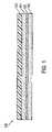
- FIG. 1is a schematic illustration of the general design of a tamper indicating RFID label according to an embodiment of the invention.
- FIG. 1shows schematically a pressure sensitive (i.e. self-adhesive) label 100 in cross sectional view.
- the label 100may include four functionally distinct layers.
- the RFID layer 101may be a layer, which includes RFID components, for example, an RFID memory chip.
- the label 100may in some embodiments provide an “active” RFID capability, in which case the layer 101 can also include a battery or other power source.
- the second layer 102may include one or more thin electrically conducting tracks which should be coupled to the RFID components in the layer 101 .
- the tracksare known herein as “tamper tracks” since they provide a means to detect tampering with or removal of the label 100 from a surface to which it has been applied.
- the layer 101 and the layer 102may together provide an RFID capability.
- the layer 101can provide an RFID capability in its own right, while the tamper tracks 102 can modify the RFID performance of the layer 101 depending on whether said tamper tracks 102 are damaged or not.
- the RFID capability provided by the layer 101usually includes the ability to store information in the RFID memory chip in the layer 101 , and the ability to read and modify said stored information from a distance. Additional capabilities, such as the ability to encrypt stored information or control access to the stored information, may also be provided.
- the third layer 103may be an adhesive layer, which in some embodiments is a pressure sensitive adhesive.
- the fourth layer 104is a top-coat layer applied over the top of the RFID layer 101 .
- the top-coatmay be applied to protect the RFID layer and to provide a top surface to accept a printing process.
- the top-coat layer 104is not essential and in some embodiments may not be included.
- the finished constructionis the adhesive label 100 .
- the tamper tracks 102should be destructible.
- the pressure sensitive adhesive 103damages the tamper tracks 102 —for example, by tearing all or part of them from the underside of the layer 101 —which in turn affects the RFID performance of the label 100 .
- the tamper tracks 102are electrically connected to the RFID components in the label 100 , and may form part of the RFID components of the label 100 , the RFID function of the label 100 is modified if the label is applied to a surface and subsequently tampered or removed. In this way tampering with or removal of the label 100 can be detected at a distance via the change in the RFID characteristics and response of the label 100 .
- stamperingand “tampered” as used herein refer to complete or partial removal of a tamper indicating label, such as the label 100 , from a surface to which it has been applied.
- destructibleis used in relation to the tamper tracks 102 in FIG. 1 and in relation to other tamper tracks throughout the document.
- destructiblemeans that the tamper tracks are designed to be damaged or broken in regions of the label which are tampered.
- conductive trackis defined herein as any circuit feature conducting electricity. Tamper tracks, destructible electronics, antennae and through hole interconnects are all forms of conductive tracks.
- the tamper tracks 102may be produced in one of a number of different ways.
- the tamper tracksmay be produced by printing electrically conducting ink (such as a carbon/graphite based conductive ink or a precious metal ink).
- the tamper tracks 102may be produced using electrically conductive adhesive.
- the tamper tracksmay be metallic tracks made of Aluminum, Copper or some other suitable metal.
- the tamper tracks 102should be made from a material, such as an electrically conducting ink, which has appropriate electrical properties but which does not have high intrinsic physical strength. In this way the tamper tracks 102 can be more easily disrupted or damaged as the label 100 is partially or completely removed from a surface to which it has been applied.
- the destructibility of the tamper tracks 102may be enhanced by including a thin layer of a suitable adhesion modifying coating on the underside of the layer 101 either between the layer 101 and the tamper tracks 102 , or between the tamper tracks 102 and the adhesive 103 . At least a part of the tamper tracks should contact the adhesive 103 .
- the layer of adhesion modifying coatingmay be applied as a uniform layer, or in a specified pattern, or in some other manner such that the properties of the adhesion modifying coating vary across the layer 101 . In some embodiments multiple layers of adhesion modifying coating may be applied to “fine tune” the properties of the final composite adhesion modifying coating.
- a adhesion modifying coating between the RFID layer 101 and the tamper tracks 102results in the adhesion of the layers to each other being greater or less in a particular region according to whether the adhesion modifying coating is present or absent in that region.
- inclusion of an adhesion modifying coating between the tamper tracks 102 and the adhesive layer 103results in the adhesion of the layers to each other being greater or less in a particular region according to whether the adhesion modifying coating is absent or present in that region.
- the adhesion modifying coatingreduces the adhesion of two layers, which it separates, so that the two layers can be more easily separated.
- the relative adhesion between the layer 101 , adhesion modifying coating, tamper tracks 102 and adhesive layer 103can be adjusted so that when the label 100 is applied to a surface and subsequently tampered or removed, the tamper tracks 102 are damaged in a pattern corresponding to the pattern of the adhesion modifying coating.
- the tamper tracks 102may be physically separated in a pattern corresponding to the pattern of the adhesion modifying coating, with some of the tamper tracks 102 remaining on the layer 101 and the remainder of the tamper tracks 102 remaining on the adhesive layer 103 . This damage to the tamper tracks 102 may affect the RFID performance of the label 100 .
- the adhesion modifying coatingmay be a layer of lacquer, or a layer of tamper indicating varnish (for example, similar to that used in some visual tamper indicating label constructions), or a layer of some other suitable material formulation.
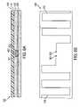
- FIG. 2shows the label 100 in cross section view before and after removal from a surface 201 .
- FIG. 2illustrates in particular the physical disruption of the tamper tracks 102 during tampering or removal of the label 100 .
- FIG. 2Athe label 100 is shown before removal from the surface 201 .
- the tamper tracks 102are intact and the label 100 exhibits its normal RFID operation.
- FIG. 2Bthe label 100 has been partially removed from the surface 201 . As the label 100 is removed, portions of the tamper tracks 102 remain with the top layer 101 , and complementary portions of the tamper tracks 102 remain with the adhesive layer 103 .
- the differential separation of the tamper tracks 102may in some embodiments be enhanced or achieved through the inclusion of an adhesion modifying coating (as described above) in a specified pattern at the interface between the layer 101 and the tamper tracks 102 , such that the tamper tracks 102 bond less strongly to the layer 101 where the adhesion modifying coating has been applied and therefore in such regions the tamper tracks 102 remain with the adhesive layer 103 when the label 100 is removed from the surface 201 .
- the tamper tracks 102are damaged, and their electrical properties are thereby affected. This in turn affects the RFID properties of the label 100 , since the tamper tracks 102 are electrically connected to the layer 101 which includes RFID components.
- FIG. 2the separation of (i.e. damage to) the tamper tracks 102 during tampering of the label 100 is shown to form a regular repeating pattern. It should be appreciated that the pattern of the separation may instead be irregular and may be on a larger or smaller scale relative to the size of the label 100 or the RFID components in the label 100 than shown in FIG. 2 .
- FIG. 3shows an embodiment of the RFID label 100 in cross sectional view ( FIG. 3A ) and looking from below through the adhesive layer 103 at the tamper tracks 102 ( FIG. 3B ).
- the RFID layer 101has two “through-connect” electrical connection points, 301 and 302 , where the electrical circuitry in the RFID layer 101 is connected to the underside of the layer 101 .
- the electrical connection between the points 301 and 302 by means of the tamper track 102should be intact in order to maintain normal RFID operation of the label 100 .
- the tamper track 102may be disrupted even if only a portion of the label 100 is tampered.
- the tamper track 102runs around the perimeter of the underside of the layer 101 between points 301 and 302 .
- the configuration for the tamper track 102 illustrated in FIG. 3ensures that tampering of even a small portion of the label 100 will result in a break in the tamper track 102 and therefore a break in the electrical connection between the points 301 and 302 , which in turn modifies the RFID behavior of the label 100 .
- the tamper track 102may form all or part of an antenna, in which case the points 301 and 302 may not be electrically connected to each other via a single tamper track 102 .
- An RFID labelwill generally include an electronic memory chip connected to either an induction loop or an antenna.
- the induction loop or antennamay enable communication and data exchange with a remote reading device. (It should be appreciated that different types of antenna design may be employed.)
- Other electrical or electronic componentsmay also be included in an RFID label.
- An active RFID labelwill include an on-board power source such as a battery.
- the tamper tracks 102may be designed to be destructible in some regions and durable in other regions.
- the tamper tracks 102may include some sections, which are durable and rugged, joined by sections which are destructible.
- the tamper tracks 102may be connected in one of several different ways to the RFID layer 101 , depending on the design and operation of the RFID layer 101 . Several non-limiting examples are listed below.
- the tamper tracks 102may be connected in series with an induction loop or antenna in the layer 101 .
- the tamper tracks 102may constitute all or part of the induction loop or antenna of the label 100 .
- the tamper tracks 102may be part of a tamper-sensing electrical circuit in the label 100 , which is separate from the induction loop or antenna of the label 100 .
- FIGS. 4 to 7are schematic illustrations of further preferred embodiments of the tamper indicating RFID label 100 , showing both a cross sectional view and a view looking from below through the adhesive layer 103 at the tamper tracks 102 .
- FIG. 4is a schematic illustration of a preferred embodiment in which the tamper track 102 connects the points 301 and 302 and is in series with an induction loop 401 in the RFID layer 101 .
- the RFID layer 101may include the induction loop 401 and other components 402 , which may be passive or active.
- the components 402in one embodiment may be a capacitor which, with the induction loop 401 , forms a resonant electrical circuit.
- the components 402may include a passive electronic memory chip for storing data.
- the tamper track 102should be intact for the RFID label 100 of FIG. 4 to be operational. When the label 100 is tampered, the tamper track 102 is broken and the RFID function of the label 100 can be disabled or modified. In this way it can be determined whether or not the label 100 has been tampered.
- An adhesion modifying coatingmay be included, as described above, to enhance destructibility of the tamper track 102 .
- FIG. 5is a schematic illustration of another preferred embodiment in which the tamper track 102 forms an induction loop 501 for the RFID label 100 .
- the through-connect points 301 and 302are connected to the RFID components 402 in the layer 101 .
- the tamper track 102forms a number of loops, with the overall layout of the tamper track 102 acting as an induction loop. Tampering or removing the label 100 results in a break in the tamper track 102 , thereby disabling or modifying the RFID function of the label 100 . In this way it can be determined whether or not the label 100 has been tampered.
- An adhesion modifying coatingmay be included, as described above, to enhance destructibility of the tamper tracks 102 .
- FIG. 6is a schematic illustration of another preferred embodiment, which is a variation on the embodiment of FIG. 5 .
- the tamper tracks 102form an antenna
- the tamper track 102forms an induction loop.
- the principal differenceis that in FIG. 6 the points 301 and 302 are not connected together by a single tamper track 102 . Instead there are two tamper tracks 102 , one starting at point 301 and the other starting at the point 302 .
- the two tamper tracks 102form an antenna.
- a so-called meander antennais illustrated, although it should be appreciated that other forms of antenna may also be employed.
- the points 301 and 302may be connected to each other by the tamper track 102 .
- the through-connect points 301 and 302are connected to the RFID components 402 .
- Tampering the label 100should result in damage to at least one of the tamper tracks 102 , thereby affecting the characteristics of the antenna and modifying or disabling the RFID function of the label 100 . In this way it can be determined whether or not the label 100 has been tampered.
- An adhesion modifying coatingmay be included, as described above, to enhance destructibility of the tamper tracks 102 .
- FIG. 7is a schematic illustration of another preferred embodiment, based on the embodiments of FIGS. 5 and 6 .
- the principal difference between the designs illustrated in FIGS. 5 and 6 , and the design illustrated in FIG. 7is that in the design of FIG. 7 the RFID components 402 are on the underside of the layer 101 .
- the RFID components 402may comprise only an RFID memory chip, in which case in the design of FIG. 7 , both the RFID memory chip 402 and the tamper tracks 102 are on the underside of the layer 101 .
- the tamper tracksare designed to be destructible, as described herein.
- An advantage of the design of FIG. 7 compared with the designs of FIGS. 5 and 6is that in the design of FIG.
- the tamper tracks 102may form an induction loop, as in the design of FIG. 5 , or may form an antenna, as in the design of FIG. 6 . In FIG. 7 an antenna is shown.
- An adhesion modifying coatingmay be included, as described above, to enhance destructibility of the tamper tracks 102 .
- the label 100may be designed to show visual evidence of tampering if the label is removed from a surface to which it has been applied.
- Visual tamper indicationcan be achieved in several ways.
- a thin colored layeris applied to the underside of the RFID layer 101 .
- a pattern of adhesion-modifying layermay be applied to the underside of the colored layer.
- the adhesion-modifying layermay be the same layer or a layer in addition to the adhesion modifying coating described above. The presence of the adhesion-modifying layer modifies the adhesion of the colored layer to the adhesive layer 103 such that when the label 100 is removed from a surface to which it has been applied, the colored layer breaks up.
- Areas of colormay adhere to the adhesive layer 103 and other complementary areas of color may adhere to the RFID layer 101 .
- An alternative to this embodimentis to apply a pattern of said adhesion modifying layer directly to the underside of the RFID layer 101 and apply said thin colored layer to the underside of said adhesion modifying layer.
- the adhesion modifying coatingmay be applied directly to the underside of the RFID layer 101 and a colored adhesive can be used as the adhesive layer 103 .
- the colored adhesive 103should break up and areas of the colored adhesive may adhere to the RFID layer 101 and complementary areas of the colored adhesive 103 may adhere to the surface. It should be appreciated that other methods may be used to produce a visual tamper indicating effect.
- a portion of the RFID layer 101 and top coat 104should be transparent so the visual effect can be seen by looking through the RFID layer 101 and top coat 104 . This enables easy inspection of the visual tamper indicating feature without having to remove the label.
- the RFID components in the RFID layer 101such as a memory chip, may not be transparent, but should only occupy a small portion of the surface area.
- FIG. 8is a schematic illustration of another preferred embodiment in which the tamper track 102 forms part of a separate tamper indicating electrical circuit.
- the RFID layer 101may contain an induction loop or antenna 801 and other electronic components 402 , including an electronic memory chip, to provide an RFID capability.
- the RFID layer 101should be capable of interacting with an RFID reading device to allow reading of or modification to data stored in the electronic memory chip.
- the through-connect points 301 and 302are connected to the components 402 in the layer 101 , and to each other via the tamper track 102 .
- the components 402should be configured to respond differently to a signal from an RFID reader depending on whether or not the points 301 and 302 are connected to each other via the tamper track 102 or not.
- the label 100will respond in a specified manner to an RFID reader.
- the label 100should still respond to an RFID reader but in a different manner, thereby indicating that the label 100 has been tampered.
- the label 100 of FIG. 8can provide an RFID means to (i) determine whether the label 100 is present, (ii) read data from the label 100 and modify data stored in the label 100 , and (iii) determine whether the label 100 has been tampered.
- the components 402may consist only of a passive RFID electronic memory chip, and the tamper track 102 forms a connection, which may be separate from the induction loop or antenna 801 , between two contact points on the memory chip.
- An adhesion modifying coatingmay be applied between the RFID layer 101 and the adhesive layer 103 , in a manner as described in relation to FIGS. 1 to 7 .
- the components 402may undergo an irreversible change if the label 100 is tampered and the tamper track 102 is damaged, so that even if the tamper track 102 is subsequently restored, the label 100 will still respond to an RFID reader with a signal indicating it has been tampered.
- the RFID components 402is “active” (i.e. powered) and is configured to test the integrity of the tamper track 102 either continuously or at specified intervals. In this embodiment if the RFID components 402 detect that the tamper track 102 has been disrupted they may then preferably be configured to record data to this effect in the electronic memory chip within the components 402 , preferably in a manner which is permanent and irreversible.
- the components 402may also include a clock.
- the date and time of any tampering of the tamper track 102 or label 100may also preferably be recorded permanently and irreversibly in the electronic memory chip within the RFID components 402 .
- FIG. 8A preferred embodiment of the tamper indicating RFID label configuration of FIG. 8 will now be described by way of non-limiting example with reference to the schematic illustrations shown in FIG. 9 .
- antennamay refer to a conventional antenna or to an induction loop (which is used as an antenna at some RFID operating frequencies).
- FIG. 9is a schematic illustration of a tamper indicating RFID label 900 shown in top view ( FIG. 9A ), cross sectional side view ( FIG. 9B ), and bottom view ( FIG. 9C ).
- the label 900may include a substrate layer 901 made of, for example, polyester or some other suitable material. On top of the substrate layer 901 , electronics to form an RFID transponder, which provides an RFID function, may be applied.
- the electronicsmay include an RFID electronic memory chip 902 and an antenna 903 . (In FIG. 9 an antenna 903 in the form of an induction loop is shown.)
- FIG. 9Dis a more detailed schematic illustration of an example of the electrical connections to the electronic chip 902 .
- the chip 902 and antenna 903should provide an RFID capability, which may include the ability to store information in the chip 902 , the ability to read information from the chip 902 at a distance using a suitable RFID device, and the ability to modify information in the chip 902 from a distance using a suitable RFID device.
- the chip 902may include two contact points, or contact pads, connected to the antenna 903 , as illustrated in FIG. 9D .
- Two contact pads on the chip 902can be connected via electrical “through-connects” 904 to the underside of the substrate layer 901 .
- One or both or neither of these two contact padsmay be the same as the contact pads used to connect the chip 902 to the antenna 903 .
- FIG. 9Dshows the through-connects 904 directly beneath the chip 902 . It should be appreciated that other configurations may instead be used for the through-connects 904 .
- the through-connects 904are positioned away from the contact pads on the chip 902 , and electrical tracks on the top surface of the substrate layer 901 connect the contact pads on the chip 902 to the tops of the through-connects 904 .
- the two through-connect points 904 on the underside of the substrate layer 901are connected to each other by means of a tamper track 905 which is positioned on the underside of the substrate layer 901 .
- a layer of adhesive 906may also be applied to the underside of the substrate layer 901 and tamper track 905 .
- said adhesive 906is a pressure sensitive adhesive.
- a top layer 907may be applied over the top of the substrate 901 , chip 902 and antenna 903 .
- the top layer 907can provide protection for these components and can also provide a surface to accept printing—for example printing of a number, a barcode, a logo, or other image.
- FIG. 9the top view ( FIG. 9A ) is a view looking through the top layer 907
- the side view ( FIG. 9B )is a cross sectional side view
- the bottom view ( FIG. 9C )is a view looking though the adhesive layer 906 .
- the tamper track 905is preferably applied to the underside of the substrate layer 901 , along with one or more layers of adhesion modifying coating to enhance the destructibility of the tamper track 905 . Consequently, if the label 900 is applied to a surface and subsequently removed, the tamper track 905 should be broken or disrupted so as to interrupt the electrical connection between the through-connect points 904 on the underside of the substrate layer 901 .
- Application of the tamper track 905 and any other adhesion modifying coatings to the underside of the substrate 901 to enhance the destructible nature of the tamper track 905may preferably be carried out as described herein and in the above-identified provisional patent applications, which are incorporated by reference.
- the tamper track 905may be laid out in a number of different ways on the underside of the substrate layer 901 .
- the tamper trackruns from one through-connect point 904 almost all the way around the perimeter of the underside of the substrate layer 901 and then back to the other through-connect point, with the outward and return paths of the tamper track 905 very close together in order to avoid any electrical induction effects which may interfere with the antenna 903 positioned above on the upper surface of the substrate layer 901 .
- the width and thickness of the tamper track 905can be adjusted to provide the correct properties in terms of electrical resistance and physical destructibility.
- the path made by the tamper track 905may run inside, or outside, or directly beneath the antenna 903 , which in FIG. 9 is an induction loop.
- the tamper track 905forms a path which is outside the outer perimeter of the induction loop 903 , thereby ensuring that any disturbance around the perimeter of the label 900 will cause the tamper track 905 to be disrupted.
- the tamper track 905When the label 900 is applied to a surface, the tamper track 905 is intact and the corresponding contact pads on the chip 902 are electrically connected to each other. When the label 900 is removed or substantially tampered with, the tamper track 905 should be broken or disrupted and there will then be an open circuit between the corresponding contact pads on the chip 902 . When such an open circuit occurs, the function of the RFID chip 902 or the information stored in the chip 902 will be modified in a way which can be detected by an RFID reader.
- the modified chip function or informationcan be detected during the first read operation of the label after the label 900 is removed or tampered, and the reader (if it has a write capability) can be programmed to write data back to the chip 902 to indicate that the label 900 has been removed or tampered.
- Said data which is written back to the chip 902 to indicate removal or tampering of the label 900is preferably permanent and irreversible, to prevent the memory contents of the chip being altered back to the original state to disguise the fact that the label has been moved or tampered.
- an RFID read/write devicecapable of detecting the change in RFID performance of the label 900 when the label 900 is tampered, and writing data back to the chip 902 within the label 900 to indicate such tampering has occurred, said data preferably being written into the chip 902 so as to be permanent and irreversible.
- the label 900can be configured such that any disruption to the tamper track 905 can be detected internally within the label 900 without requiring an RFID read operation.
- the chip 902can be programmed to modify its own memory contents to indicate that the label 900 has been removed or tampered. Said modification to the memory contents of the chip 902 to indicate removal or tampering of the label 900 should preferably be permanent and irreversible, to prevent the memory contents of the chip being altered back to the original state to disguise the fact that the label has been moved or tampered.
- the label 900may function as a normal REID label when it is first applied to a surface. After the label is moved or tampered, the RFID function of the label 900 may be maintained and information can be read from and written to the REID chip 902 , while the label also provides an RFID means to determine that it has been moved or tampered.
- Controlling the relative adhesion between the layers of the transponder constructionis critical to achieving the desired performance of the above-described tamper indicating device.
- the reasons for this and the methodologies to achieveare presented by means of a non-limiting example of a particular preferred embodiment. It is appreciated that the same concepts presented here apply to other embodiments as well.
- FIG. 10is a schematic illustration of a tamper indicating RFID label 900 as shown in FIG. 9 .
- FIG. 10Aillustrates a top view of the antenna layer 903 and the RFID device 902
- FIG. 10Cillustrates a bottom view of the tamper track layer 905 and the through connects 904 .
- FIG. 10Billustrates a side view with the adhesion modifying layer 1001 specifically shown.
- the adhesion modifying layer 1001is applied to the bottom of substrate 901 , between the substrate 901 and tamper track 905 .
- a release liner layer 1002is shown on the bottom side of adhesive layer 906 .
- This release liner layeris typically applied during the fabrication of the tamper indicating RFID label 900 and subsequently removed when the said label is applied to an object.
- the purpose of the release lineris to carry the RFID label 900 and prevent the adhesive layer 906 from inadvertently adhering to any surface prior to the label 900 being applied to a surface or object.
- the adhesion modifying layer 1001is designed such that its adhesion to the substrate 901 is weaker than that of tamper track.
- the tamper trackwill preferably have substantially strong adhesion to the substrate 901 and to the adhesion modifying layer 1001 .
- the adhesion of the tamper track 905 to the substrate 901will preferably be stronger than the adhesion of the adhesive layer 906 to the tamper track 905 .
- the adhesion modifying layer 1001will fail (i.e., separate) at the interface to the substrate 901 , thereby transferring the adhesion modifying coating 1001 and portions of the tamper track 905 in contact with the adhesion modifying coating 1001 to the adhesive layer 906 .
- the adhesive layer 906will separate from the tamper track 905 , leaving those regions of the tamper track 905 in contact with the substrate 901 .
- the adhesion of the adhesion modifying layer 1001 to the substrate 901must be sufficiently strong to prevent delamination or separation between the said layers during the transponder manufacturing processes, subsequent handling, removal of the release liner layer 1002 and application to the intended surface.
- the tamper indicating transponder 900is subjected to thermal, mechanical and other stresses. Examples of these include, but are not limited to the following: application of subsequent layers, thermal or radiation exposure, mechanical assembly, die cutting, splicing, hole formation, slitting, unwinding rewinding.
- the transpondermay also be subjected to thermal and mechanical stresses during handling and shipping.
- the adhesion of the adhesion modifying layer 1001 to the substrate 901can be controlled by the formulation of the adhesion modifying material, as will be discussed in a following section of this patent, as well as by the features of the release coating layer 1001 pattern.
- these featuresinclude, but are not limited to the following: regions containing geometric shapes of solid areas of adhesion modifying coating, regions containing geometric shapes completely absent of adhesion modifying coating, and regions containing an alternating pattern of geometric features with and without adhesion modifying material.
- FIG. 10Dillustrates an example of a preferred embodiment of the adhesion modifying layer 1001 pattern as viewed from the bottom of the tamper indicating RFID label 900 through the adhesive layer 906 (not shown) and release liner layer 1002 (not shown).
- the adhesion modifying layer 1001 patterncontains the following features: a grid pattern comprised of lines and spaces, a solid border at the perimeter of the substrate layer 901 , relatively large regions absent of any adhesion modifying coating.
- the grid patternis comprised of lines and spaces, oriented at an angle relative to the perimeter of the substrate layer 901 . It is appreciated that there are many angles at which the pattern may be oriented relative to the perimeter and/or the tamper track. Angles of 90°, 45° and 22.5° are examples. The angle affects the printing of the adhesion modifying layer during manufacturing as well as the release (destruction) characteristics during application. The width of the lines and spaces can be varied to adjust the dimensions of the area of substrate 901 covered by the adhesion modifying coating layer 1001 versus the dimensions of the area of substrate 901 in direct contact with the tamper track layer 905 .
- a relatively large area of substrate 901 in direct contact with the tamper tack layer 905will produce a relatively strong adhesion between these two layers and therefore generate an overall construction more resistant to inadvertent delamination while simultaneously less susceptible to destruction of the tamper track layer 905 in the application.
- a relatively large area of substrate 901 covered by adhesion modifying coating layer 1001will generate an overall construction more susceptible to inadvertent delamination but also more likely to result in the intended destruction of tamper track layer 905 in the application.
- adhesion modifying coating patternscan be employed, including but not limited to patterns of lines, dots, and other geometric shapes with the adhesion modifying coating, with the same or different shapes in the regions with adhesion modifying coating. It is appreciated that the dimensions of the regions with material may be different from those without material. Patterns of lines, circles and triangles have been tested. The table below provides a non-limiting example of grid patterns, which have been evaluated:
- the destructibility of layers 1001 and 905 , and the level of adhesion between the label 900 and the surface to which it is applied,can also be varied across the label 900 by varying the pattern of the adhesion modifying coating layer 1001 , and more specifically by varying the density of the pattern of the said adhesion modifying coating.
- Increasing the density of the adhesion modifying coating patterndecreases the overall adhesion strength between the label 900 and the surface to which it is applied.
- the increased densitymay result in large regions of solid release coating, such as the solid border of layer 1001 illustrated in FIG. 10D .
- larger areas without adhesion modifying coatingcan be employed.
- the adhesion modifying layer 1001is applied to the substrate 901 already in the format of its final dimensions, in that the perimeter of substrate 901 is the same size as the final product label 900 .
- the adhesion modifying layeris applied to the substrate layer 901 having dimensions larger than the final size of label 900 , from which the label 900 is created via by cutting the substrate 901 to the final perimeter dimensions using any one of a variety of cutting processes (e.g., die cutting, laser cutting, etc.).
- the adhesion modifying coating layer 1001may be printed larger than final perimeter dimensions, and the cutting process therefore cuts through layer 1001 in addition to the substrate layer 901 , thus producing a label 900 with adhesion modifying coating extending to the perimeter.
- FIG. 10Ddepicts relatively large oval shaped regions in layer 1001 absent of adhesion modifying coating. These regions are positioned diagonally at the four corners and orthogonally on two sides. It is appreciated that other shapes, positions and orientations could be employed.
- the label 900is applied to a cardboard surface and later removed, it is possible that the cardboard will begin to delaminate, with a portion of the cardboard in contact with the adhesive layer 906 .
- the oval regions in layer 1001 absent of adhesion modifying coatingwill transfer the plane of fracture from within the cardboard to the intended plane between the adhesion modifying layer 1001 and substrate 901 .
- the use of the adhesion modifying layer pattern to control adhesion and destruction patternshas been illustrated using the particular construction of FIG. 10 wherein the tamper track is located on the opposite side of substrate 901 from the antenna 903 and the adhesion modifying layer is applied between the substrate layer 901 and the tamper track 905 . It is appreciated that the same principles apply to the other previously presented embodiments involving different tamper indicating label transponder constructions. These include, but are not limited to, constructions where the tamper track is on the same side of the substrate as the antenna, the tamper track may be integral to the antenna, or the release coating is applied between the tamper track and the adhesive.
- the destructible electronicsmay be applied to the substrate layer 901 using a transfer lamination technique.
- the destructible pattern or tamper track layer 905is created separately and then transfer laminated to the underside of the substrate layer 901 .
- a bonding adhesive layermay be applied uniformly or selectively between substrate layer 901 and tamper track layer 905 to secure the said tamper track layer to the substrate.
- the adhesion modifying layer 1001 patternis preferably applied immediately adjacent to the destructible electronics tamper track layer 905 , either before or after the application of the tamper track layer 905 to the bonding adhesive. The resulting construction will produce differential separation of the destructible electronics upon tampering of the label 900 .
- the transfer laminated destructible electronicsmay be an etched or stamped piece of continuous metal (e.g., copper, aluminum).
- the transfer laminated destructible electronicsmay be a printed electrically conductive material that may or may not include a polymer binder.
- the bonding adhesivemay be selectively applied in a pattern to the underside of the substrate 901 such that, after transfer lamination of the tamper track layer 905 , portions of the destructible layer are not attached by said bonding adhesive to the substrate 901 .
- the unattached regions of the destructible electronicslead to selective failure of the destructible electronics when the label construction 900 is tampered. In this embodiment, it may not be necessary to use an adhesion modifying coating.
- the bonding adhesiveis applied uniformly to the bottom side of substrate 901 .
- the adhesion modifying layer 1001is required.
- the bonding adhesive layeris applied to the bottom side of layer 901 , onto which the tamper track layer 905 is applied.
- the adhesion modifying coating layeris applied between the tamper track layer and the adhesive layer 906 .
- the adhesion modifying coatinginhibits local delamination of the destructible electronics by the adhesive layer 906 when the label construction 900 is tampered, since in this configuration said adhesive modifying coating weakens the adhesion between the destructible electronics and the adhesive layer 906 .
- FIG. 11is a schematic illustration of the general design of a dual-transponder tamper indicating RFID label construction 1100 .
- This second tamper indicating RFID labelis designed such that when tampered it remains operational in an RFID sense, but provides information, via RFID means, to indicate that it has been tampered.
- FIG. 11shows said second tamper indicating RFID label 1100 schematically in cross sectional view.
- the label 1100includes a first RFID layer 1101 , which is a tamper indicating RFID construction of the type described in relation to FIG. 1 , so that the underside of the first RFID layer 1101 includes destructible electronics.
- a second RFID layer 1102is bonded in a permanent manner to the top surface of the first RFID layer 1101 .
- the layer 1102includes components to provide an RFID capability.
- Said second RFID layer 1102is preferably designed to be strong and durable rather than destructible.
- the second RFID layer 1102may be designed to provide a read-only RFID capability, or a read-write RFID capability, or some other RFID capability.
- the adhesive layer 1103will be a pressure sensitive adhesive, although it should be appreciated that other types of adhesive layer could be used instead.
- a top layer 1104will be applied over the top of the second RFID layer 1102 .
- the layer 1104is included to provide physical protection for the second RFID layer 1102 and to provide a surface to accept printing processes (where appropriate).
- the combined construction of the FIG. 11is tamper indicating, so that an attempt, using methods such as those described above in relation to FIG. 1 , to partially or completely remove the label 1100 from a surface to which it has been applied will result either in a break in the destructible electronics of the first RFID layer 1101 , or distortion to the destructible electronics, or a disruption to the connection between the destructible electronics and the RFID chip in the first RFID layer 1101 , or other modification to the first RFID layer 1101 to the extent that the RFID function of the first RFID layer 1101 is modified in a manner detectable by an RFID reader or read/write device.
- the RFID function of the second RFID layer 1102will preferably be unaltered by tampering of the label 1100 , since damage due to tampering will usually be confirmed to the region of the bottom surface of the first RFID layer 1101 and the adhesive layer 1103 .
- FIG. 12illustrates schematically ways in which the first RFID layer 1101 and second RFID layer 1102 of FIG. 11 can be configured.
- the layers 1101 and 1102 of FIG. 11will each include an electronic chip. Typically the chip will be significantly thicker than the rest of the layer.
- the layer 1101includes the electronic chip 1201
- the layer 1102includes the electronic chip 1202 which is positioned on the top surface of the layer 1102 .
- FIG. 12Aillustrates schematically two cross sectional views of preferred embodiments of the tamper indicating RFID label 1100 in which the RFID chip 1201 is on the top surface of the layer 1101 .
- the layer 1101is longer than the layer 1102 , and the chip 1201 is positioned to the side of, rather than underneath, the layer 1102 so as to allow the layer 1101 to be bonded evenly to the layer 1102 across the entire bottom surface of the layer 1102 .
- the layer 1102includes a hole and the layer 1101 is positioned under the layer 1102 such that the chip 1201 is in said hole, thereby enabling the layer 1101 to be bonded evenly to the layer 1102 across the entire bottom surface of the layer 1102 .
- the benefit of the design of FIG. 12 A( 2 )is that it provides a more uniform top surface to the layer 1102 , on which top surface a top layer may be applied.
- An adhesive layer 1103is applied to the bottom surface of the first REID layer 1101 .
- the adhesive layer 1103is a pressure sensitive adhesive, although it should be appreciated that other types of adhesive layer could be used.
- a top layer 1104may be applied to the top surface of the second RFID layer 1102 .
- the top layer 1104may be applied in order to protect the layer 1102 and also in order to provide a surface to accept printing.
- FIG. 12Billustrates schematically a cross sectional view of a preferred embodiment of the tamper indicating RFID label 1100 in which the RFID chip 1201 is on the bottom surface of the layer 1101 .
- the mating surfaces of the RFID layers 1101 and 1102are both flat and even, and the layers 1101 and 1102 can be bonded together across the entire mating surface of the layers without difficulty.
- An adhesive layer 1103is applied to the bottom surface of the layer 1101 such that the chip 1201 and destructible electronics on the bottom surface of the layer 1101 are sandwiched between the layer 1101 and the adhesive 1103 .
- the adhesive layer 1103is a pressure sensitive adhesive, although it should be appreciated that other types of adhesive layer could be used.
- a top layer 1104is applied to the top surface of the layer 1102 .
- the top layer 1104may be applied to protect the layer 1102 and also to provide a surface to accept a printing process.
- the performance of the RFID layer 1101 and 1102may be adversely affected by the proximity of the other layer. This can occur especially when the antennas or induction loops in the layers 1101 and 1102 are in close proximity.
- the antenna or induction loop in the tamper indicating RFID layer 1101may in some preferred embodiments be separated laterally from the antenna or induction loop in the RFID layer 1102 , rather than being placed directly beneath the antenna or induction loop in the layer 1102 . This is illustrated schematically in FIG.
- the antenna or induction loop of the layer 1102is positioned in the region 1204
- the antenna or induction loop 1101is positioned mainly in the region 1203
- some preferred embodimentsalso including a portion of the destructible electronics on the bottom surface of the layer 1101 extending into the region 1204 in order to provide the tamper indicating function of the layer 1101 across all portions of the label construction 1100 .
- the two substrates 1101 and 1102may be replaced by a single substrate.
- the durable transpondermay be fabricated directly on the top surface of said substrate and the destructible transponder may be fabricated directly on the bottom surface of said substrate.
- the destructible transpondermay be constructed using any of the methodologies described herein.
- FIG. 13is schematic illustration of said second tamper indicating RFID label in which both electronic chips are positioned on the top side of the single substrate layer.
- the electronic chip 1302 of said destructible transponderis on the top side 1303 of the substrate 1301 and the destructible electronics of said destructible transponder are on the underside 1304 of the substrate 1301 , with one or more through-connects 1305 connecting the top and bottom layers 1303 and 1304 of the substrate 1301 .
- a durable transponderis applied to the top surface 1303 of the substrate 1301 , so that the electronic chip 1306 of the durable transponder is also on the top surface 1303 of the substrate 1301 .
- An adhesive layer 1307is applied to the underside of the substrate layer 1301 .
- a top layer 1308may be applied to the top surface of the substrate 1301 , such that the electronic chips 1302 and 1306 and any other electronics on the top surface 1303 of the substrate 1301 are covered over and protected.
- said top layer 1308may be a layer designed to accept a printing process.
- the two transponders in the construction illustrated in FIG. 13may be displaced laterally to avoid transponder interference, as described above.
- the durable transponder and destructible transpondermay be fabricated using two different electrical conductor technologies.
- the durable transpondermay be fabricated using etched metal (e.g., copper or aluminum) electrical conductors, and the destructible transponder could be conducted using any of the conductor technologies described herein.
- the durable transponder and destructible transpondermay operate at different frequencies or use different RFID protocols, or both.
- Operating the two transponders at different frequenciesoffers several potential advantages. As discussed above, when two transponders operating at the same frequency are placed in close proximity, the two antenna coils or induction loops have a de-tuning effect on each other which can result in the read distance for each transponder being reduced from the normal operating range. The magnitude of this effect will depend on the operating frequency, antenna geometry and position of one transponder relative to the other. For instance, when two similar transponders are placed directly on top of each other, the read distance for each may be substantially reduced.
- Two transponders operating at two different frequenciesusually have a lesser de-tuning effect on each other than two transponders operating at the same frequency. For instance, it can be demonstrated that placing a 2.45 GHz transponder in the center of a 13.56 MHz transponder coil will have minimal effect on the performance of either transponder.
- Another potential benefit of using different frequencies for the two transpondersis reduced label size. For instance, even when placed adjacent to each other (rather than on top of each other or one within the other), a combination of a 2.45 GHz transponder and a 13.56 MHz transponder will be smaller than two adjacent 13.56 MHz transponders, simply due to the smaller size of the 2.45 GHz transponder.
- one chipcould be an industry standard chip while the other could be a custom chip, said custom chip incorporating enhanced features, functionally or security and being visible (in an RFID sense) only to especially configured RFID readers.
- the dual transponder constructionwould “look” like a standard single transponder construction to a standard RFID reader.
- the adhesion modifying layer 1001is comprised of an adhesion modifying material applied according to the previously described methodologies.
- the formulation of the said materialaffects the relative adhesion strengths between the different layers and therefore affects the performance of the tamper indicating RFID label.
- a typical formulation of said adhesion modifying coatingis as follows.
- the polymer resincan be a thermoplastic resin such as a phenoxy resin (for example, Paphen® PKHC manufactured by Phenoxy Specialties).
- thermosetting resin compositionsmay also be employed.
- radiation cured formulationscan be used, such as free radical initiated acrylate or methacrylate systems based on acrylated or methacrylated oligomers.
- free radical initiated acrylate or methacrylate systemsbased on acrylated or methacrylated oligomers.
- acrylated or methacrylated epoxy, urethane and polyester oligomers or cationic initiated systems based on vinyl ethers, epoxies, cycloaliphatic epoxies, epoxidized oils and rubbersmay be used.
- the diluentwhich is selected based on compatibility with the chosen resin, the viscosity of the solution, speed of drying and ease of printing, can be water and/or an organic solvent.
- glycol ethers or glycol ether acetatessuch as di(ethylene glycol) butyl ether (butyl carbitol) and di(ethylene glycol) ethyl ether acetate (carbitol acetate), dibasic esters such as dimethyl adipate, dimethyl succinate or dimethyl glutarate, gamma butyrolactone, n-methyl pyrrolidinone, aromatics such as toluene and xylene, ketones such as methyl ethyl ketone and isophorone or mixtures thereof, may be used.
- the diluentmay include reactive diluents in addition to or in place of the water or organic solvent, such as low viscosity glycols (for example, diethylene, triethylene, dipropylene or tripropylene glycol), polyglycols (for example, polyethylene, polytetramethylene or polypropylene glycol) and polyester polyols (for example, Tone® polyols available from Union Carbide).
- low viscosity glycolsfor example, diethylene, triethylene, dipropylene or tripropylene glycol
- polyglycolsfor example, polyethylene, polytetramethylene or polypropylene glycol
- polyester polyolsfor example, Tone® polyols available from Union Carbide.
- free radical initiated formulationslow viscosity acrylate or methacrylate monomers are used. In some instances when using a low viscosity resin or oligomer the diluent may be omitted entirely.
- thermosetting and radiation cured formulasalso employ a catalyst.
- the catalystcan be a blocked organic or inorganic acid, such as Nacure® 2530 manufactured by King Industries.
- Epoxy formulationsemploy catalysts or hardeners such as anhydrides (for example, Methylhexahydrophthaliic anhydride), tertiary amine or imidazole catalysts (for example, Imicure® AMI-2 manufactured by Air Products and Chemicals), dicyandiamide and amine, amidoamine or modified amine hardeners (for example, ANCAMINE® 2337S manufactured by Air Products and Chemicals).
- anhydridesfor example, Methylhexahydrophthaliic anhydride
- tertiary amine or imidazole catalystsfor example, Imicure® AMI-2 manufactured by Air Products and Chemicals
- dicyandiamide and aminefor example, amidoamine or modified amine hardeners (for example, ANCAMINE® 2337S manufactured by Air Products and Chemicals).
- the Ultraviolet/visible light formulasare cured using free radical or cationic photoinitiators, such as Irgacure® 184 manufactured by Ciba specialty chemicals or Cyracure® UVI 6992 manufactured by Union Carbide. Electron beam cured formulasdo not require a catalyst.
- Fillersare used alone or in combination to control the viscosity and rheology of the coating for ease of application.
- Inert fillerssuch as talc, silica, kaolin, calcium carbonate or barium sulfate may be added.
- Thixotropic fillerssuch as synthetic silica can also be used (for example, Aerosil® R-202 manufactured by Degussa).
- Flow control additivestypically include materials such as surfactants and leveling agents. These ingredients contribute to the wetting of the substrate and the quality of the coating surface.
- Typical Flow control additivesare modified silicone oils such as BYK Chemie's BYK® 323 or non-silicone leveling agents such as Modaflow® manufactured by Solutia.
- Typical surfactantsare fluorocarbons such as FC430 manufactured by 3M or silicone materials such as BYK® 307.
- one ingrediente.g., a surfactant
- FC430manufactured by 3M
- silicone materialssuch as BYK® 307.
- one ingrediente.g., a surfactant
- one or more of the major ingredientse.g., diluent or polymer might provide the performance attribute normally provided by these minor ingredients.
- Defoamersare chemicals added to control the formation of foam during mixing and application of the coating.
- a typical defoameris BYK® 075.
- silicone or non silicone leveling agentsmay provide the performance attributes of a defoamer or air release agent.
- colorantssuch as dyes (e.g organic dyes), inorganic, organic or organometallic pigments or mixtures, solutions or dispersions thereof may also be added.
- dyese.g organic dyes
- organic or organometallic pigments or mixturese.g., Polytrend® colorant dispersions manufactured by Creanova.
- a coatingwas prepared using the following ingredients.
- the phenoxy resinis dissolved in the solvent with stirring and heating to 50–60° C.
- the mixtureis cooled to 25° C. and the defoamer and colorant added.
- the solutionis further mixed to combine the ingredients.
- example 1The coating of example 1 was applied to 0.05 mm thick untreated polyethylene terephthalate film through a patterned 300 mesh stainless steel screen using standard screen printing technology.
- the screen meshwas selected to produce a dry ink film thickness (DIFT) of between 3 and 7 microns, 4–5 microns being the typical DIFT. Stainless steel or polymer mesh screens are acceptable.
- DIFTdry ink film thickness
- Stainless steel or polymer mesh screensare acceptable.
- the applied coatingwas cured in a conveyor oven at 120° C. for 60 seconds.
- a subtractive techniquecan be used. These formulas are commonly referred to as photo imagable wherein the coating is applied as a solid continuous layer. This layer is then exposed to the radiation through a mask or phototool containing the desired pattern. The areas of the coating where the radiation is not blocked by the mask are cured and remain intact. The areas of the coating where the radiation is blocked remain uncured and are subsequently removed by a developer. Developers are typically organic solvents, water or aqueous solutions of an inorganic base (for example, Sodium Carbonate).
- a preferred method of manufacture of a preferred embodiment of the inventionare illustrated by way of a non-limiting example using the construction of tamper indicating label 900 as depicted in FIGS. 10A , 10 B, 10 C, and 10 D. It is appreciated that the methods described herein are typical approaches and other methods familiar to those practiced in the art may also be employed.
- Each layer of the transponder designis step and repeated to create a multi-up layout on large area, such as 18 by 24 inches, in order to economically manufacture multiple pieces on each sheet of material processed. It is appreciated that multiple pieces will be processed for each step described below. It is also appreciated that typical manufacturing practices will process multiple sheets sequentially at each process step.
- the substrate layer 901is comprised of Polyethylene terephtalate (PET) film.
- PETPolyethylene terephtalate
- the PET filmis heat stabilized to relieve mechanical stresses and reduce dimension instability as a function of temperature exposure.
- the holes for the through connects 904are then formed by laser, drilling or punching.
- the antenna layer 903is applied to the top surface of the substrate 901 by screen printing a conductive polymer thick film ink (e.g. silver filled ink).
- a conductive polymer thick film inke.g. silver filled ink.
- the polymer thick film inkis then thermally cured.
- a layer of insulting dielectricis then screen printed over the antenna layer 903 and UV cured to form the insulating cross-over layer.
- a second layermay be applied in a similar fashion.
- a layer of conductive polymer thick film inke.g., silver filled ink
- the filling of the through connect holes 904may be accomplished at the same process step or by an addition printing and curing step.
- the cross-over layeris consider to be a part of antenna layer 903 .
- the adhesion modifying layer 1001is then applied to the bottom surface of substrate 901 by screen printing and thermally curing the adhesion modifying material.
- the tamper track 905is then formed by screen printing and thermally curing a conductive polymer thick film ink (e.g., silver filled ink).
- the RFID memory device(usually referred to as an RFID “chip”) 902 is applied to the top surface of the substrate 901 by applying an anisotropic conductive adhesive paste to the chip location, placing the chip into said paste, and curing said paste via thermal compression bonding to form both a mechanical and electrical connection between the chip 902 , substrate 901 and antenna 903 .
- the assembled constructionmay be tested for functionality, after which the sheet is cut into strips which are then spliced together to form a roll of transponders.
- the adhesive layer 906 and release liner layer 1002are then applied to the bottom of the substrate 901 , adhesion modifying layer 1001 and tamper track layer 905 .
- the top layeris then applied to the top of the substrate 901 , over the chip 902 and antenna 903 .
- a tamper indicating transponder labelcan be created using an active or passive RF device.
- materials, methods and constructions described hereinmay be utilized to create tamper indicating circuitry containing non-RF devices or no discrete electronic devices at all.
Landscapes
- Engineering & Computer Science (AREA)
- Physics & Mathematics (AREA)
- Computer Security & Cryptography (AREA)
- General Physics & Mathematics (AREA)
- Automation & Control Theory (AREA)
- Electromagnetism (AREA)
- Computer Hardware Design (AREA)
- General Engineering & Computer Science (AREA)
- Microelectronics & Electronic Packaging (AREA)
- Theoretical Computer Science (AREA)
- Manufacturing & Machinery (AREA)
- Credit Cards Or The Like (AREA)
- Laminated Bodies (AREA)
Abstract
Description
| Line Width | Gap Width | Orientation of grid |
| (inches) | (inches) | to tamper track |
| 0.020 | 0.020 | Orthogonal | (90°/0°) |
| 0.020 | 0.030 | Orthogonal | (90°/0°) |
| 0.020 | 0.040 | Orthogonal | (90°/0°) |
| 0.020 | 0.020 | Angled | (22.5°) |
| 0.020 | 0.030 | Angled | (22.5°) |
| 0.020 | 0.040 | Angled | (22.5°) |
| Weight % | |||
| Component | Range | Preferred | ||
| Polymer resin or oligomer | 5–97 | 15–65 | ||
| Diluent | 0–80 | 25–80 | ||
| Catalyst | 0–10 | 0–7 | ||
| Filler | 0–30 | 0–20 | ||
| Colorant | 0–1.0 | 0.1–1.0 | ||
| Flow control additive | 0.0–2.0 | 0.05–1.5 | ||
| Defoamer | 0.01–1.0 | 0.05–0.5 | ||
It should be noted that not all of the above components are necessarily present in every formulation.
| TABLE 2 | |||
| Approx. | |||
| Component | Weight % | ||
| Resin | 25.4 | ||
| Phenoxy Resin (Paphen ® PKHC) | |||
| Diluent | 74.1 | ||
| (Di(ethylene glycol) ethyl ether acetate) | |||
| Defoamer | 0.1 | ||
| (BYK ® 075) | |||
| Colorant | 0.4 | ||
| (Phthalocyanine Blue 12% dispersion) | |||
| Polytrend ® 850-7240 | |||
Claims (48)
Priority Applications (3)
| Application Number | Priority Date | Filing Date | Title |
|---|---|---|---|
| US09/915,760US7049962B2 (en) | 2000-07-28 | 2001-07-26 | Materials and construction for a tamper indicating radio frequency identification label |
| AU2001279041AAU2001279041A1 (en) | 2000-07-28 | 2001-07-27 | Materials and construction for a tamper indicating radio frequency identification label |
| CA002417616ACA2417616C (en) | 2000-07-28 | 2001-07-27 | Materials and construction for a tamper indicating radio frequency identification label |
Applications Claiming Priority (3)
| Application Number | Priority Date | Filing Date | Title |
|---|---|---|---|
| US22164000P | 2000-07-28 | 2000-07-28 | |
| US23621800P | 2000-09-28 | 2000-09-28 | |
| US09/915,760US7049962B2 (en) | 2000-07-28 | 2001-07-26 | Materials and construction for a tamper indicating radio frequency identification label |
Publications (2)
| Publication Number | Publication Date |
|---|---|
| US20020036237A1 US20020036237A1 (en) | 2002-03-28 |
| US7049962B2true US7049962B2 (en) | 2006-05-23 |
Family
ID=26915976
Family Applications (1)
| Application Number | Title | Priority Date | Filing Date |
|---|---|---|---|
| US09/915,760Expired - LifetimeUS7049962B2 (en) | 2000-07-28 | 2001-07-26 | Materials and construction for a tamper indicating radio frequency identification label |
Country Status (5)
| Country | Link |
|---|---|
| US (1) | US7049962B2 (en) |
| EP (1) | EP1309959A4 (en) |
| AU (1) | AU2001279041A1 (en) |
| CA (1) | CA2417616C (en) |
| WO (1) | WO2002011094A1 (en) |
Cited By (77)
| Publication number | Priority date | Publication date | Assignee | Title |
|---|---|---|---|---|
| US20050057424A1 (en)* | 2003-07-10 | 2005-03-17 | Vesa Kukko | Planar antenna |
| US20050068180A1 (en)* | 2003-07-10 | 2005-03-31 | Jarkko Miettinen | Usage modification of RFID transponder |
| US20050121421A1 (en)* | 2001-10-02 | 2005-06-09 | Neil Kirby | Method of manufacturing circuits |
| US20060000891A1 (en)* | 2004-07-01 | 2006-01-05 | American Express Travel Related Services Company, Inc. | System for biometric security using a smartcard |
| US20060000892A1 (en)* | 2004-07-01 | 2006-01-05 | American Express Travel Related Services Company, Inc. | Method for biometric security using a smartcard |
| US20060016870A1 (en)* | 2004-07-01 | 2006-01-26 | American Express Travel Related Services Company, Inc. | Method and system for smellprint recognition biometrics on a smartcard |
| US20060016877A1 (en)* | 2004-07-01 | 2006-01-26 | American Express Travel Related Services Company, Inc. | Biometric safeguard method with a smartcard |
| US20060016875A1 (en)* | 2004-07-01 | 2006-01-26 | American Express Travel Related Services Company, Inc. | Method for registering a biometric for use with a smartcard |
| US20060226985A1 (en)* | 2005-02-08 | 2006-10-12 | Goodnow Timothy T | RF tag on test strips, test strip vials and boxes |
| US20060232424A1 (en)* | 2003-03-07 | 2006-10-19 | Checkpoint Systems International Gmbh | Security label and method for safeguarding objects |
| US20060290512A1 (en)* | 2005-06-22 | 2006-12-28 | Smurfit-Stone Container Enterprises, Inc. | Methods and apparatus for RFID transponder fabrication |
| US20070011870A1 (en)* | 2005-07-18 | 2007-01-18 | Lerch John W | Method of manufacture of an identification wristband construction |
| US20070060311A1 (en)* | 2005-09-12 | 2007-03-15 | Igt | Enhanced gaming chips and table game security |
| US20070069899A1 (en)* | 2005-09-26 | 2007-03-29 | Chin-Ming Shih | Flexible radio frequency identification label and method for fabricating the same |
| US20070115129A1 (en)* | 2005-11-23 | 2007-05-24 | Kessler John R | Deactivatable RFID labels and tags and methods of making same |
| US20070120687A1 (en)* | 2005-11-29 | 2007-05-31 | Lerch John W | Identification band using a conductive fastening for enhanced security and functionality |
| US20070152822A1 (en)* | 2005-12-29 | 2007-07-05 | International Business Machines Corporation | Monitoring device for detecting opening of packaging |
| US20070252704A1 (en)* | 2006-04-13 | 2007-11-01 | Tsuyoshi Nagae | RFID label |
| US20070257801A1 (en)* | 2006-04-13 | 2007-11-08 | Tsuyoshi Nagae | RFID label, tag tape roll, RFID circuit element cartridge |
| US7303120B2 (en)* | 2001-07-10 | 2007-12-04 | American Express Travel Related Services Company, Inc. | System for biometric security using a FOB |
| US20080016002A1 (en)* | 2001-07-10 | 2008-01-17 | American Express Travel Related Services Company, Inc. | Method for using a sensor to register a biometric for use with a transponder-reader system related applications |
| US7341185B1 (en)* | 2007-10-30 | 2008-03-11 | International Business Machines Corporation | Method of marking and monitoring products at a self-service checkout terminal |
| US20080075934A1 (en)* | 2006-08-07 | 2008-03-27 | Pliant Corporation | Tamper Event Detection Films, Systems and Methods |
| US7363504B2 (en) | 2004-07-01 | 2008-04-22 | American Express Travel Related Services Company, Inc. | Method and system for keystroke scan recognition biometrics on a smartcard |
| US7360689B2 (en)* | 2001-07-10 | 2008-04-22 | American Express Travel Related Services Company, Inc. | Method and system for proffering multiple biometrics for use with a FOB |
| US20080143519A1 (en)* | 2006-12-19 | 2008-06-19 | 3M Innovative Properties Company | Tamper-indicating radio frequency identification tag and methods of indicating tampering of a radio frequency identification tag |
| US20080248382A1 (en)* | 2007-03-30 | 2008-10-09 | The Regents Of The University Of Michigan | Deposited Microarchitectured Battery and Manufacturing Method |
| US20080272885A1 (en)* | 2004-01-22 | 2008-11-06 | Mikoh Corporation | Modular Radio Frequency Identification Tagging Method |
| US20080303640A1 (en)* | 2007-06-05 | 2008-12-11 | Heiko Rommelmann | Hybrid system option key |
| US20090022999A1 (en)* | 2007-07-19 | 2009-01-22 | Luzenac America, Inc. | Silicone coatings, methods of making silicone coated articles and coated articles therefrom |
| US20090128340A1 (en)* | 2007-11-21 | 2009-05-21 | Masin Joseph V | Tamper resistant RFID tags and associated methods |
| US7543738B1 (en) | 2001-07-10 | 2009-06-09 | American Express Travel Related Services Company, Inc. | System and method for secure transactions manageable by a transaction account provider |
| US7557715B1 (en)* | 2006-02-08 | 2009-07-07 | Tc License Ltd. | Destructible RFID transponder |
| US7639116B2 (en) | 2001-07-10 | 2009-12-29 | Peter D Saunders | Converting account data associated with a radio frequency device |
| US20100018640A1 (en)* | 2006-12-21 | 2010-01-28 | Gisela Simons | Method for applying markings to substrate surfaces by means of a transfer method |
| US7668750B2 (en) | 2001-07-10 | 2010-02-23 | David S Bonalle | Securing RF transactions using a transactions counter |
| US7705732B2 (en) | 2001-07-10 | 2010-04-27 | Fred Bishop | Authenticating an RF transaction using a transaction counter |
| US7725427B2 (en) | 2001-05-25 | 2010-05-25 | Fred Bishop | Recurrent billing maintenance with radio frequency payment devices |
| US7735725B1 (en) | 2001-07-10 | 2010-06-15 | Fred Bishop | Processing an RF transaction using a routing number |
| US7814332B2 (en) | 2001-07-10 | 2010-10-12 | Blayn W Beenau | Voiceprint biometrics on a payment device |
| US7889052B2 (en) | 2001-07-10 | 2011-02-15 | Xatra Fund Mx, Llc | Authorizing payment subsequent to RF transactions |
| US20110043339A1 (en)* | 2009-08-19 | 2011-02-24 | Intelleflex Corporation | RF device with tamper detection |
| US20110174885A1 (en)* | 2008-07-15 | 2011-07-21 | Syntag Manufacturing, LLC | Durable rfid tag |
| US8001054B1 (en) | 2001-07-10 | 2011-08-16 | American Express Travel Related Services Company, Inc. | System and method for generating an unpredictable number using a seeded algorithm |
| US20110210030A1 (en)* | 2009-01-07 | 2011-09-01 | Meadwestvaco Corporation | Security packaging |
| US8029443B2 (en) | 2003-07-15 | 2011-10-04 | Abbott Diabetes Care Inc. | Glucose measuring device integrated into a holster for a personal area network device |
| US8029927B2 (en) | 2005-03-22 | 2011-10-04 | Blue Spark Technologies, Inc. | Thin printable electrochemical cell utilizing a “picture frame” and methods of making the same |
| USRE43157E1 (en) | 2002-09-12 | 2012-02-07 | Xatra Fund Mx, Llc | System and method for reassociating an account number to another transaction account |
| US8279042B2 (en) | 2001-07-10 | 2012-10-02 | Xatra Fund Mx, Llc | Iris scan biometrics on a payment device |
| US8294552B2 (en) | 2001-07-10 | 2012-10-23 | Xatra Fund Mx, Llc | Facial scan biometrics on a payment device |
| US8441411B2 (en) | 2007-07-18 | 2013-05-14 | Blue Spark Technologies, Inc. | Integrated electronic device and methods of making the same |
| US8444058B2 (en) | 2011-01-20 | 2013-05-21 | Trovan, Ltd. | Embedded RFID tags and associated methods and systems |
| US8460243B2 (en) | 2003-06-10 | 2013-06-11 | Abbott Diabetes Care Inc. | Glucose measuring module and insulin pump combination |
| WO2013101654A1 (en)* | 2011-12-27 | 2013-07-04 | The Gillette Company | Radio frequency identification tag |
| US8574754B2 (en) | 2007-12-19 | 2013-11-05 | Blue Spark Technologies, Inc. | High current thin electrochemical cell and methods of making the same |
| US8618938B2 (en) | 2011-11-21 | 2013-12-31 | Trovan, Ltd. | Gas cylinder and RFID transponder assemblies and related methods having fixed transponder orientations |
| US8722235B2 (en) | 2004-04-21 | 2014-05-13 | Blue Spark Technologies, Inc. | Thin printable flexible electrochemical cell and method of making the same |
| US8722233B2 (en) | 2005-05-06 | 2014-05-13 | Blue Spark Technologies, Inc. | RFID antenna-battery assembly and the method to make the same |
| US8765284B2 (en) | 2012-05-21 | 2014-07-01 | Blue Spark Technologies, Inc. | Multi-cell battery |
| US8991709B2 (en) | 2010-08-30 | 2015-03-31 | Tagstar Systems Gmbh | Tamper-proof RFID label |
| US9024719B1 (en) | 2001-07-10 | 2015-05-05 | Xatra Fund Mx, Llc | RF transaction system and method for storing user personal data |
| US9027242B2 (en) | 2011-09-22 | 2015-05-12 | Blue Spark Technologies, Inc. | Cell attachment method |
| US9031880B2 (en) | 2001-07-10 | 2015-05-12 | Iii Holdings 1, Llc | Systems and methods for non-traditional payment using biometric data |
| US9041540B2 (en) | 2012-02-29 | 2015-05-26 | International Business Machines Corporation | Radio frequency identification tag gripper device |
| US9444078B2 (en) | 2012-11-27 | 2016-09-13 | Blue Spark Technologies, Inc. | Battery cell construction |
| US9454752B2 (en) | 2001-07-10 | 2016-09-27 | Chartoleaux Kg Limited Liability Company | Reload protocol at a transaction processing entity |
| US9607189B2 (en) | 2015-01-14 | 2017-03-28 | Tactilis Sdn Bhd | Smart card system comprising a card and a carrier |
| US20170166369A1 (en)* | 2013-03-15 | 2017-06-15 | Altria Client Services Llc | Label having tear strip |
| US9693689B2 (en) | 2014-12-31 | 2017-07-04 | Blue Spark Technologies, Inc. | Body temperature logging patch |
| US9782082B2 (en) | 2012-11-01 | 2017-10-10 | Blue Spark Technologies, Inc. | Body temperature logging patch |
| US10037528B2 (en) | 2015-01-14 | 2018-07-31 | Tactilis Sdn Bhd | Biometric device utilizing finger sequence for authentication |
| US10395227B2 (en) | 2015-01-14 | 2019-08-27 | Tactilis Pte. Limited | System and method for reconciling electronic transaction records for enhanced security |
| US10849501B2 (en) | 2017-08-09 | 2020-12-01 | Blue Spark Technologies, Inc. | Body temperature logging patch |
| US10963417B2 (en) | 2004-06-04 | 2021-03-30 | Abbott Diabetes Care Inc. | Systems and methods for managing diabetes care data |
| US11281952B2 (en) | 2019-06-04 | 2022-03-22 | Trovan, Ltd. | Systems and methods to secure transponders within RFID tags without potting elements |
| US11461610B2 (en) | 2020-08-28 | 2022-10-04 | Trovan, Ltd. | Apparatus and methods for retrofitting an object with an RFID transponder |
| US11534089B2 (en) | 2011-02-28 | 2022-12-27 | Abbott Diabetes Care Inc. | Devices, systems, and methods associated with analyte monitoring devices and devices incorporating the same |
Families Citing this family (59)
| Publication number | Priority date | Publication date | Assignee | Title |
|---|---|---|---|---|
| US7306158B2 (en) | 2001-07-10 | 2007-12-11 | American Express Travel Related Services Company, Inc. | Clear contactless card |
| FR2823310B1 (en)* | 2001-04-05 | 2004-05-14 | Arjo Wiggins Sa | STICKER DOCUMENT INCORPORATING A RADIO FREQUENCY IDENTIFICATION DEVICE |
| US6758405B2 (en)* | 2001-12-19 | 2004-07-06 | 3M Innovative Properties Company | Article with retroreflective and radio frequency-responsive features |
| EP1363233A1 (en)* | 2002-05-13 | 2003-11-19 | Orell Füssli Sicherheitsdruck AG | Security document having a resonant circuit |
| JP4342771B2 (en)* | 2002-05-15 | 2009-10-14 | リンテック株式会社 | IC tag |
| US20040061655A1 (en)* | 2002-08-07 | 2004-04-01 | Forster Ian J. | Environmentally sensitive multi-frequency antenna |
| JP3948660B2 (en)* | 2002-08-27 | 2007-07-25 | 富士フイルム株式会社 | Recording medium cartridge |
| US7294917B2 (en) | 2002-11-21 | 2007-11-13 | Lintec Corporation | IC tag |
| GB0229124D0 (en)* | 2002-12-13 | 2003-01-15 | Hills Numberplates Ltd | Signs |
| US7102522B2 (en) | 2002-12-24 | 2006-09-05 | 3M Innovative Properties Company | Tamper-indicating radio frequency identification antenna and sticker, a radio frequency identification antenna, and methods of using the same |
| US6995674B2 (en)* | 2003-02-28 | 2006-02-07 | Saxon, Inc. | Package assembly |
| US6816125B2 (en) | 2003-03-01 | 2004-11-09 | 3M Innovative Properties Company | Forming electromagnetic communication circuit components using densified metal powder |
| US7098792B1 (en)* | 2003-05-14 | 2006-08-29 | Rf Technologies, Inc. | Tamper proof system and method |
| JP3945476B2 (en)* | 2003-12-02 | 2007-07-18 | セイコーエプソン株式会社 | Contactless data communication system and contactless identification tag |
| US7259678B2 (en) | 2003-12-08 | 2007-08-21 | 3M Innovative Properties Company | Durable radio frequency identification label and methods of manufacturing the same |
| US20050159222A1 (en)* | 2003-12-18 | 2005-07-21 | Matthew Pasulka | Data plate |
| CN1898686A (en)* | 2003-12-24 | 2007-01-17 | 新加坡科技物资管理私人有限公司 | Rfid sealing label |
| US7250868B2 (en)* | 2004-03-12 | 2007-07-31 | A K Stamping Co. Inc. | Manufacture of RFID tags and intermediate products therefor |
| JP4596844B2 (en)* | 2004-07-23 | 2010-12-15 | テルモ株式会社 | Medical article and ordering system for medical article |
| US7229018B2 (en)* | 2004-08-03 | 2007-06-12 | Kurz Arthur A | Manufacture of RFID tags and intermediate products therefor |
| US7956752B2 (en)* | 2005-01-14 | 2011-06-07 | Matthew Henderson | Transponder bolt seal and a housing for a transponder |
| DE602006004494D1 (en) | 2005-04-20 | 2009-02-12 | Ibm | System and method for manipulation detection |
| WO2006124400A2 (en)* | 2005-05-13 | 2006-11-23 | University Of Pittsburgh - Of The Commonwealth System Of Higher Education | Method of making an electronic device using an electrically conductive polymer, and associated products |
| US7571862B2 (en)* | 2005-06-02 | 2009-08-11 | Avery Dennison Corporation | RFID tag that provides a flat print area and a pinch roller that enables the same |
| WO2006133380A2 (en)* | 2005-06-07 | 2006-12-14 | University Of Pittsburgh - Of The Commonwealth System Of Higher Education | Manufacturing of electronic devices using conductive polymer |
| US7546948B2 (en)* | 2005-09-14 | 2009-06-16 | Meadwestvaco Corporation | Identification device and method |
| US7224278B2 (en)* | 2005-10-18 | 2007-05-29 | Avery Dennison Corporation | Label with electronic components and method of making same |
| US7410103B2 (en)* | 2006-03-13 | 2008-08-12 | Andreas Rolf Nagel | System, method and device to detect product tampering |
| ATE452325T1 (en) | 2006-06-30 | 2010-01-15 | Ibm | DEVICE FOR SECURING A SURVEY MARKER BASED ON THE USE OF A HIGH FREQUENCY IDENTIFICATION LABEL |
| US20080048434A1 (en)* | 2006-07-06 | 2008-02-28 | S&C Electric Co. | Apparatus and method for authenticating fuse products |
| DE502006004394D1 (en)* | 2006-10-09 | 2009-09-10 | Schreiner Group Gmbh & Co Kg | RFID tag |
| DE102006052517A1 (en)* | 2006-11-06 | 2008-05-08 | Bielomatik Leuze Gmbh + Co.Kg | Chip module for an RFID system |
| US8212677B2 (en)* | 2007-02-12 | 2012-07-03 | Alexander Ferguson | Automated medication management system and method for use |
| US20080290176A1 (en)* | 2007-05-22 | 2008-11-27 | Precision Dynamics Corporation | Methods and devices with a circuit for carrying information on a host |
| CN101755292A (en)* | 2007-06-15 | 2010-06-23 | 马修·亨德森 | Transponder bolt seal and housing for a transponder |
| EP3364501A1 (en)* | 2007-07-04 | 2018-08-22 | Murata Manufacturing Co., Ltd. | Wireless ic device and component for wireless ic device |
| TW200905753A (en)* | 2007-07-18 | 2009-02-01 | Yuen Foong Yu Paper Mfg Co Ltd | Flexible and super-thin smart card and packaging method thereof |
| FR2923050B1 (en)* | 2007-10-30 | 2011-09-23 | Oberthur Card Syst Sa | AUTHENTICATION OF AN ELECTRONIC LABEL BY ASSOCIATION WITH AN ENTITY, ASSOCIATED METHODS, SYSTEMS AND LABEL. |
| WO2009080420A1 (en) | 2007-12-20 | 2009-07-02 | International Business Machines Corporation | System and method to locate rfid devices |
| CN101896924A (en) | 2007-12-20 | 2010-11-24 | 国际商业机器公司 | System and method for determining RFID tagged items encompassed in a given area |
| DE102008027560A1 (en)* | 2008-06-10 | 2009-12-24 | Lin, Chih-Cheng, Sinhua | Maintenance system for vehicle, has wireless data transmission unit for wirelessly receiving data, and central processing unit detecting rank according to transmission signal and transmitting data corresponding to rank |
| US8207820B2 (en) | 2008-06-24 | 2012-06-26 | International Business Machines Corporation | Location localization method and system |
| PL2164032T3 (en)* | 2008-09-15 | 2019-01-31 | Hueck Folien Ges.M.B.H. | Manipulation-proof RFID antenna with safety feature |
| DE102009021722B4 (en)* | 2009-05-18 | 2011-05-19 | Schreiner Group Gmbh & Co. Kg | Label, use of a printing ink for a label and method for producing a label |
| US20120032394A1 (en)* | 2010-08-05 | 2012-02-09 | Levine Jonathan E | Electronic game piece |
| US9129202B2 (en)* | 2010-11-15 | 2015-09-08 | Orpak Systems Ltd. | Device for automated fuel delivery authorization and method for installation thereof |
| JP6073048B2 (en)* | 2011-07-04 | 2017-02-01 | 東洋アルミニウム株式会社 | RFID inlet antenna and RFID using the same |
| TWI444899B (en)* | 2011-09-16 | 2014-07-11 | Favite Inc | Rfid tag structure having anti-reuse function and manufacture method thereof |
| TWI453677B (en)* | 2011-12-01 | 2014-09-21 | Mutual Pak Technology Co Ltd | Radio frequency identification tag and cloth having the same |
| US9324020B2 (en)* | 2012-08-30 | 2016-04-26 | Nxp B.V. | Antenna structures and methods for omni directional radiation patterns |
| JP2014134997A (en)* | 2013-01-11 | 2014-07-24 | Nippon Package System Kk | Film antenna and method for manufacturing the same, and rfid label |
| DE102013005486B4 (en) | 2013-04-02 | 2019-02-14 | Heraeus Deutschland GmbH & Co. KG | Layer structure with conductive polymer for tamper detection as well as method for its production |
| US9313195B2 (en) | 2013-09-30 | 2016-04-12 | Protegrity Corporation | Collision avoidance in a distributed tokenization environment |
| US9111116B2 (en) | 2013-09-30 | 2015-08-18 | Protegrity Corporation | Collision avoidance in a distributed tokenization environment |
| US9370401B2 (en)* | 2014-05-12 | 2016-06-21 | Philip W. Sayles | Millimeter-sized recognition signal badge and identification system for accurately discerning and sorting among similar kinds, shapes, and sizes of surgical instruments |
| US9679237B2 (en)* | 2015-09-22 | 2017-06-13 | Pallettechnology, Inc. | Board embedded with electronic device |
| US11288561B2 (en)* | 2019-11-07 | 2022-03-29 | CoreKinect LLC | Methods and apparatus for a security sticker anti-tampering system |
| CN116745775A (en)* | 2021-02-17 | 2023-09-12 | 富士通先端科技株式会社 | RFID tag |
| WO2023217358A1 (en)* | 2022-05-10 | 2023-11-16 | Assa Abloy Ab | Rfid tag for a tamper proof attachment to an object such as a licence plate |
Citations (17)
| Publication number | Priority date | Publication date | Assignee | Title |
|---|---|---|---|---|
| US3671721A (en)* | 1968-12-12 | 1972-06-20 | Revenue Systems Ltd | Data reading systems |
| US4029945A (en)* | 1975-08-27 | 1977-06-14 | Stanley Electric Co., Ltd. | Card and card reader apparatus therefor |
| US4740536A (en) | 1985-09-06 | 1988-04-26 | Rohm And Haas Company | Water-based binder, coating and adhesive compositions from alkaline-curable latex polymers, epoxies and amines |
| US4752680A (en)* | 1984-11-20 | 1988-06-21 | Saab Automation Ab | Tags for identification system |
| US5358982A (en) | 1992-08-06 | 1994-10-25 | Hoechst Aktiengesellschaft Ag | Crosslinked polymer microparticles based on epoxy resin, their preparation and their use |
| US5442334A (en) | 1992-07-20 | 1995-08-15 | Stoplift Corporation | Security system having deactivatable security tag |
| US5567760A (en) | 1994-11-15 | 1996-10-22 | The Dow Chemical Company | Films from aqueous dispersions of block copolymers having hydrogenated conjugated diene block |
| US5604485A (en)* | 1993-04-21 | 1997-02-18 | Motorola Inc. | RF identification tag configurations and assemblies |
| US5644295A (en)* | 1994-09-05 | 1997-07-01 | Permasign Limited | Security device |
| US5767772A (en) | 1993-12-15 | 1998-06-16 | Lemaire; Gerard | Marker for an article which is detected when it passes through a surveillance zone |
| US5777003A (en) | 1994-11-10 | 1998-07-07 | Wacker-Chemie Gmbh | Redispersible polymer powder composition comprising cyclodextrins or cyclodextrin derivitaves |
| US5834538A (en) | 1996-06-18 | 1998-11-10 | Hercules Incorporated | Pressure sensitive adhesives |
| US6050622A (en)* | 1991-12-19 | 2000-04-18 | Gustafson; Ake | Safety sealing device |
| US6110551A (en) | 1995-04-07 | 2000-08-29 | William Exline, Inc. | Adhesive strip for use in a wallet size card book |
| US6147604A (en) | 1998-10-15 | 2000-11-14 | Intermec Ip Corporation | Wireless memory device |
| US6242512B1 (en) | 1996-01-18 | 2001-06-05 | Wacker Chemie Gmbh | Re-dispersible polymer powder and aqueous polymer dispersions obtainable therefrom |
| US6255958B1 (en) | 1998-05-05 | 2001-07-03 | H-G-Tek Ltd. | Anti-theft electronic tag |
Family Cites Families (5)
| Publication number | Priority date | Publication date | Assignee | Title |
|---|---|---|---|---|
| US5406263A (en)* | 1992-07-27 | 1995-04-11 | Micron Communications, Inc. | Anti-theft method for detecting the unauthorized opening of containers and baggage |
| ATE165767T1 (en)* | 1994-02-15 | 1998-05-15 | Owens Illinois Labels Inc | MULTI-LAYER LABEL |
| KR100498670B1 (en)* | 1996-05-14 | 2005-11-01 | 다이니폰 인사츠 가부시키가이샤 | Thermal Transfer Award Sheet |
| JP3883264B2 (en)* | 1997-09-08 | 2007-02-21 | 大日本印刷株式会社 | Thermal transfer image receiving sheet for sealing and method for producing the same |
| US5982284A (en)* | 1997-09-19 | 1999-11-09 | Avery Dennison Corporation | Tag or label with laminated thin, flat, flexible device |
- 2001
- 2001-07-26USUS09/915,760patent/US7049962B2/ennot_activeExpired - Lifetime
- 2001-07-27WOPCT/US2001/023639patent/WO2002011094A1/ennot_activeApplication Discontinuation
- 2001-07-27AUAU2001279041Apatent/AU2001279041A1/ennot_activeAbandoned
- 2001-07-27EPEP01957281Apatent/EP1309959A4/ennot_activeWithdrawn
- 2001-07-27CACA002417616Apatent/CA2417616C/ennot_activeExpired - Fee Related
Patent Citations (17)
| Publication number | Priority date | Publication date | Assignee | Title |
|---|---|---|---|---|
| US3671721A (en)* | 1968-12-12 | 1972-06-20 | Revenue Systems Ltd | Data reading systems |
| US4029945A (en)* | 1975-08-27 | 1977-06-14 | Stanley Electric Co., Ltd. | Card and card reader apparatus therefor |
| US4752680A (en)* | 1984-11-20 | 1988-06-21 | Saab Automation Ab | Tags for identification system |
| US4740536A (en) | 1985-09-06 | 1988-04-26 | Rohm And Haas Company | Water-based binder, coating and adhesive compositions from alkaline-curable latex polymers, epoxies and amines |
| US6050622A (en)* | 1991-12-19 | 2000-04-18 | Gustafson; Ake | Safety sealing device |
| US5442334A (en) | 1992-07-20 | 1995-08-15 | Stoplift Corporation | Security system having deactivatable security tag |
| US5358982A (en) | 1992-08-06 | 1994-10-25 | Hoechst Aktiengesellschaft Ag | Crosslinked polymer microparticles based on epoxy resin, their preparation and their use |
| US5604485A (en)* | 1993-04-21 | 1997-02-18 | Motorola Inc. | RF identification tag configurations and assemblies |
| US5767772A (en) | 1993-12-15 | 1998-06-16 | Lemaire; Gerard | Marker for an article which is detected when it passes through a surveillance zone |
| US5644295A (en)* | 1994-09-05 | 1997-07-01 | Permasign Limited | Security device |
| US5777003A (en) | 1994-11-10 | 1998-07-07 | Wacker-Chemie Gmbh | Redispersible polymer powder composition comprising cyclodextrins or cyclodextrin derivitaves |
| US5567760A (en) | 1994-11-15 | 1996-10-22 | The Dow Chemical Company | Films from aqueous dispersions of block copolymers having hydrogenated conjugated diene block |
| US6110551A (en) | 1995-04-07 | 2000-08-29 | William Exline, Inc. | Adhesive strip for use in a wallet size card book |
| US6242512B1 (en) | 1996-01-18 | 2001-06-05 | Wacker Chemie Gmbh | Re-dispersible polymer powder and aqueous polymer dispersions obtainable therefrom |
| US5834538A (en) | 1996-06-18 | 1998-11-10 | Hercules Incorporated | Pressure sensitive adhesives |
| US6255958B1 (en) | 1998-05-05 | 2001-07-03 | H-G-Tek Ltd. | Anti-theft electronic tag |
| US6147604A (en) | 1998-10-15 | 2000-11-14 | Intermec Ip Corporation | Wireless memory device |
Cited By (168)
| Publication number | Priority date | Publication date | Assignee | Title |
|---|---|---|---|---|
| US7725427B2 (en) | 2001-05-25 | 2010-05-25 | Fred Bishop | Recurrent billing maintenance with radio frequency payment devices |
| US7705732B2 (en) | 2001-07-10 | 2010-04-27 | Fred Bishop | Authenticating an RF transaction using a transaction counter |
| US7814332B2 (en) | 2001-07-10 | 2010-10-12 | Blayn W Beenau | Voiceprint biometrics on a payment device |
| US7543738B1 (en) | 2001-07-10 | 2009-06-09 | American Express Travel Related Services Company, Inc. | System and method for secure transactions manageable by a transaction account provider |
| US8074889B2 (en) | 2001-07-10 | 2011-12-13 | Xatra Fund Mx, Llc | System for biometric security using a fob |
| US8279042B2 (en) | 2001-07-10 | 2012-10-02 | Xatra Fund Mx, Llc | Iris scan biometrics on a payment device |
| USRE45416E1 (en) | 2001-07-10 | 2015-03-17 | Xatra Fund Mx, Llc | Processing an RF transaction using a routing number |
| US7506819B2 (en) | 2001-07-10 | 2009-03-24 | Xatra Fund Mx, Llc | Biometric security using a fob |
| US8284025B2 (en) | 2001-07-10 | 2012-10-09 | Xatra Fund Mx, Llc | Method and system for auditory recognition biometrics on a FOB |
| US9024719B1 (en) | 2001-07-10 | 2015-05-05 | Xatra Fund Mx, Llc | RF transaction system and method for storing user personal data |
| US8001054B1 (en) | 2001-07-10 | 2011-08-16 | American Express Travel Related Services Company, Inc. | System and method for generating an unpredictable number using a seeded algorithm |
| US7988038B2 (en) | 2001-07-10 | 2011-08-02 | Xatra Fund Mx, Llc | System for biometric security using a fob |
| US8289136B2 (en) | 2001-07-10 | 2012-10-16 | Xatra Fund Mx, Llc | Hand geometry biometrics on a payment device |
| US8294552B2 (en) | 2001-07-10 | 2012-10-23 | Xatra Fund Mx, Llc | Facial scan biometrics on a payment device |
| US8548927B2 (en) | 2001-07-10 | 2013-10-01 | Xatra Fund Mx, Llc | Biometric registration for facilitating an RF transaction |
| US7578448B2 (en) | 2001-07-10 | 2009-08-25 | Blayn W Beenau | Authorizing radio frequency transactions using a keystroke scan |
| US7637434B2 (en)* | 2001-07-10 | 2009-12-29 | Blayn W Beenau | Registering a biometric for radio frequency transactions |
| US7500616B2 (en) | 2001-07-10 | 2009-03-10 | Xatra Fund Mx, Llc | Authenticating fingerprints for radio frequency payment transactions |
| US10839388B2 (en) | 2001-07-10 | 2020-11-17 | Liberty Peak Ventures, Llc | Funding a radio frequency device transaction |
| US7303120B2 (en)* | 2001-07-10 | 2007-12-04 | American Express Travel Related Services Company, Inc. | System for biometric security using a FOB |
| US7506818B2 (en) | 2001-07-10 | 2009-03-24 | Xatra Fund Mx, Llc | Biometrics for radio frequency payment transactions |
| US9031880B2 (en) | 2001-07-10 | 2015-05-12 | Iii Holdings 1, Llc | Systems and methods for non-traditional payment using biometric data |
| US7889052B2 (en) | 2001-07-10 | 2011-02-15 | Xatra Fund Mx, Llc | Authorizing payment subsequent to RF transactions |
| US7886157B2 (en) | 2001-07-10 | 2011-02-08 | Xatra Fund Mx, Llc | Hand geometry recognition biometrics on a fob |
| US7639116B2 (en) | 2001-07-10 | 2009-12-29 | Peter D Saunders | Converting account data associated with a radio frequency device |
| US20080016002A1 (en)* | 2001-07-10 | 2008-01-17 | American Express Travel Related Services Company, Inc. | Method for using a sensor to register a biometric for use with a transponder-reader system related applications |
| US7735725B1 (en) | 2001-07-10 | 2010-06-15 | Fred Bishop | Processing an RF transaction using a routing number |
| US9336634B2 (en) | 2001-07-10 | 2016-05-10 | Chartoleaux Kg Limited Liability Company | Hand geometry biometrics on a payment device |
| US7690577B2 (en) | 2001-07-10 | 2010-04-06 | Blayn W Beenau | Registering a biometric for radio frequency transactions |
| US9454752B2 (en) | 2001-07-10 | 2016-09-27 | Chartoleaux Kg Limited Liability Company | Reload protocol at a transaction processing entity |
| US7668750B2 (en) | 2001-07-10 | 2010-02-23 | David S Bonalle | Securing RF transactions using a transactions counter |
| US7360689B2 (en)* | 2001-07-10 | 2008-04-22 | American Express Travel Related Services Company, Inc. | Method and system for proffering multiple biometrics for use with a FOB |
| US7642126B2 (en)* | 2001-10-02 | 2010-01-05 | Poly-Flex Circuits Limited | Method of manufacturing circuits |
| US20050121421A1 (en)* | 2001-10-02 | 2005-06-09 | Neil Kirby | Method of manufacturing circuits |
| USRE43157E1 (en) | 2002-09-12 | 2012-02-07 | Xatra Fund Mx, Llc | System and method for reassociating an account number to another transaction account |
| US7450011B2 (en)* | 2003-03-07 | 2008-11-11 | Checkpoint Systems, Inc. | Security tag and method for securing articles |
| US20060232424A1 (en)* | 2003-03-07 | 2006-10-19 | Checkpoint Systems International Gmbh | Security label and method for safeguarding objects |
| US8460243B2 (en) | 2003-06-10 | 2013-06-11 | Abbott Diabetes Care Inc. | Glucose measuring module and insulin pump combination |
| US20050057424A1 (en)* | 2003-07-10 | 2005-03-17 | Vesa Kukko | Planar antenna |
| US7469126B2 (en)* | 2003-07-10 | 2008-12-23 | Upm Raflatac Oy | Usage modification of RFID transponder |
| US20050068180A1 (en)* | 2003-07-10 | 2005-03-31 | Jarkko Miettinen | Usage modification of RFID transponder |
| US8029443B2 (en) | 2003-07-15 | 2011-10-04 | Abbott Diabetes Care Inc. | Glucose measuring device integrated into a holster for a personal area network device |
| US20080272885A1 (en)* | 2004-01-22 | 2008-11-06 | Mikoh Corporation | Modular Radio Frequency Identification Tagging Method |
| US8722235B2 (en) | 2004-04-21 | 2014-05-13 | Blue Spark Technologies, Inc. | Thin printable flexible electrochemical cell and method of making the same |
| US11182332B2 (en) | 2004-06-04 | 2021-11-23 | Abbott Diabetes Care Inc. | Systems and methods for managing diabetes care data |
| US11507530B2 (en) | 2004-06-04 | 2022-11-22 | Abbott Diabetes Care Inc. | Systems and methods for managing diabetes care data |
| US12056079B2 (en) | 2004-06-04 | 2024-08-06 | Abbott Diabetes Care Inc. | Systems and methods for managing diabetes care data |
| US10963417B2 (en) | 2004-06-04 | 2021-03-30 | Abbott Diabetes Care Inc. | Systems and methods for managing diabetes care data |
| US9922320B2 (en) | 2004-07-01 | 2018-03-20 | Iii Holdings 1, Llc | System and method of a smartcard transaction with biometric scan recognition |
| US20060000891A1 (en)* | 2004-07-01 | 2006-01-05 | American Express Travel Related Services Company, Inc. | System for biometric security using a smartcard |
| US7497375B2 (en) | 2004-07-01 | 2009-03-03 | American Express Travel Related Services Company, Inc. | Smartcard transaction method and system using smellprint recognition |
| US8016191B2 (en) | 2004-07-01 | 2011-09-13 | American Express Travel Related Services Company, Inc. | Smartcard transaction system and method |
| US7506806B2 (en) | 2004-07-01 | 2009-03-24 | American Express Travel Related Services Company, Inc. | Smartcard transaction method and system using fingerprint recognition |
| US7510115B2 (en) | 2004-07-01 | 2009-03-31 | American Express Travel Related Services Company, Inc. | Smartcard transaction method and system using auditory scan recognition |
| US7523860B2 (en) | 2004-07-01 | 2009-04-28 | American Express Travel Related Services Company, Inc. | Smartcard transaction method and system using facial scan recognition |
| US7530493B2 (en) | 2004-07-01 | 2009-05-12 | American Express Travel Related Services Company, Inc. | Smartcard transaction method and system using iris scan recognition |
| US20060016875A1 (en)* | 2004-07-01 | 2006-01-26 | American Express Travel Related Services Company, Inc. | Method for registering a biometric for use with a smartcard |
| US7533827B2 (en) | 2004-07-01 | 2009-05-19 | American Express Travel Related Services Company, Inc. | Smartcard transaction method and system using signature recognition |
| US20060016877A1 (en)* | 2004-07-01 | 2006-01-26 | American Express Travel Related Services Company, Inc. | Biometric safeguard method with a smartcard |
| US7494058B2 (en) | 2004-07-01 | 2009-02-24 | American Express Travel Related Services Company, Inc. | Smartcard transaction method and system using voiceprint recognition |
| US8360322B2 (en) | 2004-07-01 | 2013-01-29 | American Express Travel Related Services Company, Inc. | System and method of a smartcard transaction with biometric scan recognition |
| US7314165B2 (en)* | 2004-07-01 | 2008-01-01 | American Express Travel Related Services Company, Inc. | Method and system for smellprint recognition biometrics on a smartcard |
| US7451925B2 (en) | 2004-07-01 | 2008-11-18 | American Express Travel Related Services Company, Inc. | System for biometric security using a smartcard |
| US7325724B2 (en)* | 2004-07-01 | 2008-02-05 | American Express Travel Related Services Company, Inc. | Method for registering a biometric for use with a smartcard |
| US7451924B2 (en) | 2004-07-01 | 2008-11-18 | American Express Travel Related Services Company, Inc. | System for biometric security using a smartcard |
| US7594612B2 (en) | 2004-07-01 | 2009-09-29 | American Express Travel Related Services Company, Inc. | Smartcard transaction method and system using retinal scan recognition |
| US7597265B2 (en) | 2004-07-01 | 2009-10-06 | American Express Travel Related Services Company, Inc. | Method and system for vascular scan recognition with a smartcard |
| US7445149B2 (en) | 2004-07-01 | 2008-11-04 | American Express Travel Related Services Company, Inc. | System for biometric security using a smartcard |
| US7314164B2 (en) | 2004-07-01 | 2008-01-01 | American Express Travel Related Services Company, Inc. | System for biometric security using a smartcard |
| US20080006691A1 (en)* | 2004-07-01 | 2008-01-10 | American Express Travel Related Services Company, Inc. | Method and system for smellprint recognition biometrics on a smartcard |
| US7318550B2 (en)* | 2004-07-01 | 2008-01-15 | American Express Travel Related Services Company, Inc. | Biometric safeguard method for use with a smartcard |
| US20060000892A1 (en)* | 2004-07-01 | 2006-01-05 | American Express Travel Related Services Company, Inc. | Method for biometric security using a smartcard |
| US7363504B2 (en) | 2004-07-01 | 2008-04-22 | American Express Travel Related Services Company, Inc. | Method and system for keystroke scan recognition biometrics on a smartcard |
| US7793845B2 (en) | 2004-07-01 | 2010-09-14 | American Express Travel Related Services Company, Inc. | Smartcard transaction system and method |
| US20060016870A1 (en)* | 2004-07-01 | 2006-01-26 | American Express Travel Related Services Company, Inc. | Method and system for smellprint recognition biometrics on a smartcard |
| US7438234B2 (en) | 2004-07-01 | 2008-10-21 | American Express Travel Related Services Company, Inc. | System for biometric security using a smartcard |
| US7341181B2 (en)* | 2004-07-01 | 2008-03-11 | American Express Travel Related Services Company, Inc. | Method for biometric security using a smartcard |
| US9336423B2 (en) | 2005-02-08 | 2016-05-10 | Abbott Diabetes Care Inc. | Analyte meter including an RFID reader |
| US9907470B2 (en) | 2005-02-08 | 2018-03-06 | Abbott Diabetes Care Inc. | Analyte meter including an RFID reader |
| US8410939B2 (en) | 2005-02-08 | 2013-04-02 | Abbott Diabetes Care Inc. | Analyte meter including an RFID reader |
| US8542122B2 (en) | 2005-02-08 | 2013-09-24 | Abbott Diabetes Care Inc. | Glucose measurement device and methods using RFID |
| US8390455B2 (en) | 2005-02-08 | 2013-03-05 | Abbott Diabetes Care Inc. | RF tag on test strips, test strip vials and boxes |
| US20060226985A1 (en)* | 2005-02-08 | 2006-10-12 | Goodnow Timothy T | RF tag on test strips, test strip vials and boxes |
| US9060805B2 (en) | 2005-02-08 | 2015-06-23 | Abbott Diabetes Care Inc. | Analyte meter including an RFID reader |
| US8760297B2 (en) | 2005-02-08 | 2014-06-24 | Abbott Diabetes Care Inc. | Analyte meter including an RFID reader |
| US7545272B2 (en)* | 2005-02-08 | 2009-06-09 | Therasense, Inc. | RF tag on test strips, test strip vials and boxes |
| US8358210B2 (en) | 2005-02-08 | 2013-01-22 | Abbott Diabetes Care Inc. | RF tag on test strips, test strip vials and boxes |
| US8115635B2 (en) | 2005-02-08 | 2012-02-14 | Abbott Diabetes Care Inc. | RF tag on test strips, test strip vials and boxes |
| US8223021B2 (en) | 2005-02-08 | 2012-07-17 | Abbott Diabetes Care Inc. | RF tag on test strips, test strip vials and boxes |
| US8268475B2 (en) | 2005-03-22 | 2012-09-18 | Blue Spark Technologies, Inc. | Thin printable electrochemical cell and methods of making the same |
| US8029927B2 (en) | 2005-03-22 | 2011-10-04 | Blue Spark Technologies, Inc. | Thin printable electrochemical cell utilizing a “picture frame” and methods of making the same |
| US8722233B2 (en) | 2005-05-06 | 2014-05-13 | Blue Spark Technologies, Inc. | RFID antenna-battery assembly and the method to make the same |
| US8734980B2 (en) | 2005-05-06 | 2014-05-27 | Blue Spark Technologies, Inc. | Electrical device-battery assembly and the method to make the same |
| US20060290512A1 (en)* | 2005-06-22 | 2006-12-28 | Smurfit-Stone Container Enterprises, Inc. | Methods and apparatus for RFID transponder fabrication |
| US20070011870A1 (en)* | 2005-07-18 | 2007-01-18 | Lerch John W | Method of manufacture of an identification wristband construction |
| US20100095522A1 (en)* | 2005-07-18 | 2010-04-22 | Bartronics America, Inc. | Method of manufacture of an identification wristband construction |
| US7562445B2 (en) | 2005-07-18 | 2009-07-21 | Bartronics America, Inc. | Method of manufacture of an identification wristband construction |
| US20070060311A1 (en)* | 2005-09-12 | 2007-03-15 | Igt | Enhanced gaming chips and table game security |
| US7938722B2 (en)* | 2005-09-12 | 2011-05-10 | Igt | Enhanced gaming chips and table game security |
| US20070069899A1 (en)* | 2005-09-26 | 2007-03-29 | Chin-Ming Shih | Flexible radio frequency identification label and method for fabricating the same |
| US7385512B2 (en)* | 2005-09-26 | 2008-06-10 | Industrial Technology Research Institute | Flexible radio frequency identification label and method for fabricating the same |
| US7893839B2 (en) | 2005-11-23 | 2011-02-22 | Avery Dennison Corporation | Deactivatable RFID labels and tags and methods of making same |
| US20080180251A1 (en)* | 2005-11-23 | 2008-07-31 | Paxar Americas, Inc. | Deactivatable rfid labels and tags and methods of making same |
| US8068030B2 (en) | 2005-11-23 | 2011-11-29 | Avery Dennison Corporation | Deactivatable RFID labels and tags and methods of making same |
| US20070115129A1 (en)* | 2005-11-23 | 2007-05-24 | Kessler John R | Deactivatable RFID labels and tags and methods of making same |
| US7375635B2 (en)* | 2005-11-23 | 2008-05-20 | Paxar Americas, Inc. | Deactivatable RFID labels and tags and methods of making same |
| US20110101107A1 (en)* | 2005-11-23 | 2011-05-05 | Avery Dennison Retail Information Services Llc | Deactivatable RFID Labels and Tags and Methods of Making Same |
| US7535356B2 (en)* | 2005-11-29 | 2009-05-19 | Bartronics America, Inc. | Identification band using a conductive fastening for enhanced security and functionality |
| US20100012733A1 (en)* | 2005-11-29 | 2010-01-21 | Bartronics America, Inc. | Identification band using a conductive fastening for enhanced security and functionality |
| WO2007064430A3 (en)* | 2005-11-29 | 2007-12-21 | Proximities Inc | Identification band using a conductive fastening for enhanced security and functionality |
| US20070120687A1 (en)* | 2005-11-29 | 2007-05-31 | Lerch John W | Identification band using a conductive fastening for enhanced security and functionality |
| US20070152822A1 (en)* | 2005-12-29 | 2007-07-05 | International Business Machines Corporation | Monitoring device for detecting opening of packaging |
| US7564354B2 (en)* | 2005-12-29 | 2009-07-21 | International Business Machines Corporation | Monitoring device for detecting opening of packaging |
| US7557715B1 (en)* | 2006-02-08 | 2009-07-07 | Tc License Ltd. | Destructible RFID transponder |
| US20070252704A1 (en)* | 2006-04-13 | 2007-11-01 | Tsuyoshi Nagae | RFID label |
| US20070257801A1 (en)* | 2006-04-13 | 2007-11-08 | Tsuyoshi Nagae | RFID label, tag tape roll, RFID circuit element cartridge |
| US7812726B2 (en)* | 2006-08-07 | 2010-10-12 | Pliant Corporation | Tamper event detection films, systems and methods |
| US20080075934A1 (en)* | 2006-08-07 | 2008-03-27 | Pliant Corporation | Tamper Event Detection Films, Systems and Methods |
| US20080143519A1 (en)* | 2006-12-19 | 2008-06-19 | 3M Innovative Properties Company | Tamper-indicating radio frequency identification tag and methods of indicating tampering of a radio frequency identification tag |
| US20100018640A1 (en)* | 2006-12-21 | 2010-01-28 | Gisela Simons | Method for applying markings to substrate surfaces by means of a transfer method |
| US8430987B2 (en)* | 2006-12-21 | 2013-04-30 | Gisela Simons | Method for applying markings to substrate surfaces by means of a transfer method |
| US20080248382A1 (en)* | 2007-03-30 | 2008-10-09 | The Regents Of The University Of Michigan | Deposited Microarchitectured Battery and Manufacturing Method |
| US8231998B2 (en) | 2007-03-30 | 2012-07-31 | The Regents Of The University Of Michigan | Deposited microarchitectured battery and manufacturing method |
| US8603662B2 (en) | 2007-03-30 | 2013-12-10 | The Regents Of The University Of Michigan | Deposited microarchitectured battery and manufacturing method |
| WO2008121972A3 (en)* | 2007-03-30 | 2008-11-27 | Univ Michigan | Deposited microarchitectured battery and manufacturing method |
| US7902964B2 (en)* | 2007-06-05 | 2011-03-08 | Xerox Corporation | Hybrid system option key |
| US20080303640A1 (en)* | 2007-06-05 | 2008-12-11 | Heiko Rommelmann | Hybrid system option key |
| US8441411B2 (en) | 2007-07-18 | 2013-05-14 | Blue Spark Technologies, Inc. | Integrated electronic device and methods of making the same |
| US20090022999A1 (en)* | 2007-07-19 | 2009-01-22 | Luzenac America, Inc. | Silicone coatings, methods of making silicone coated articles and coated articles therefrom |
| US7341185B1 (en)* | 2007-10-30 | 2008-03-11 | International Business Machines Corporation | Method of marking and monitoring products at a self-service checkout terminal |
| US20090128340A1 (en)* | 2007-11-21 | 2009-05-21 | Masin Joseph V | Tamper resistant RFID tags and associated methods |
| US7855649B2 (en) | 2007-11-21 | 2010-12-21 | Masin Joseph V | Tamper resistant RFID tags and associated methods |
| US8574754B2 (en) | 2007-12-19 | 2013-11-05 | Blue Spark Technologies, Inc. | High current thin electrochemical cell and methods of making the same |
| US8763910B2 (en) | 2008-07-15 | 2014-07-01 | Syntag Manufacturing, LLC | Durable RFID tag |
| US9330352B2 (en) | 2008-07-15 | 2016-05-03 | Syntag Manufacturing, LLC | Durable RFID tag |
| US20110174885A1 (en)* | 2008-07-15 | 2011-07-21 | Syntag Manufacturing, LLC | Durable rfid tag |
| US8698627B2 (en) | 2009-01-07 | 2014-04-15 | Meadwestvaco Corporation | Security packaging |
| US20110210030A1 (en)* | 2009-01-07 | 2011-09-01 | Meadwestvaco Corporation | Security packaging |
| US9082057B2 (en)* | 2009-08-19 | 2015-07-14 | Intelleflex Corporation | RF device with tamper detection |
| US20110043339A1 (en)* | 2009-08-19 | 2011-02-24 | Intelleflex Corporation | RF device with tamper detection |
| US8991709B2 (en) | 2010-08-30 | 2015-03-31 | Tagstar Systems Gmbh | Tamper-proof RFID label |
| US8444058B2 (en) | 2011-01-20 | 2013-05-21 | Trovan, Ltd. | Embedded RFID tags and associated methods and systems |
| US11534089B2 (en) | 2011-02-28 | 2022-12-27 | Abbott Diabetes Care Inc. | Devices, systems, and methods associated with analyte monitoring devices and devices incorporating the same |
| US9027242B2 (en) | 2011-09-22 | 2015-05-12 | Blue Spark Technologies, Inc. | Cell attachment method |
| US8618938B2 (en) | 2011-11-21 | 2013-12-31 | Trovan, Ltd. | Gas cylinder and RFID transponder assemblies and related methods having fixed transponder orientations |
| WO2013101654A1 (en)* | 2011-12-27 | 2013-07-04 | The Gillette Company | Radio frequency identification tag |
| WO2014043445A3 (en)* | 2011-12-27 | 2014-06-05 | The Gillette Company | Radio frequency identification tag |
| US9041540B2 (en) | 2012-02-29 | 2015-05-26 | International Business Machines Corporation | Radio frequency identification tag gripper device |
| US8765284B2 (en) | 2012-05-21 | 2014-07-01 | Blue Spark Technologies, Inc. | Multi-cell battery |
| US9782082B2 (en) | 2012-11-01 | 2017-10-10 | Blue Spark Technologies, Inc. | Body temperature logging patch |
| US10617306B2 (en) | 2012-11-01 | 2020-04-14 | Blue Spark Technologies, Inc. | Body temperature logging patch |
| US9444078B2 (en) | 2012-11-27 | 2016-09-13 | Blue Spark Technologies, Inc. | Battery cell construction |
| US20170166369A1 (en)* | 2013-03-15 | 2017-06-15 | Altria Client Services Llc | Label having tear strip |
| US20220355987A1 (en)* | 2013-03-15 | 2022-11-10 | Altria Client Services Llc | Label having tear strip |
| US11414249B2 (en)* | 2013-03-15 | 2022-08-16 | Altria Client Services Llc | Label having tear strip |
| US12420996B2 (en)* | 2013-03-15 | 2025-09-23 | Altria Client Services Llc | Label having tear strip |
| US9693689B2 (en) | 2014-12-31 | 2017-07-04 | Blue Spark Technologies, Inc. | Body temperature logging patch |
| US10631731B2 (en) | 2014-12-31 | 2020-04-28 | Blue Spark Technologies, Inc. | Body temperature logging patch |
| US10395227B2 (en) | 2015-01-14 | 2019-08-27 | Tactilis Pte. Limited | System and method for reconciling electronic transaction records for enhanced security |
| US10275768B2 (en) | 2015-01-14 | 2019-04-30 | Tactilis Pte. Limited | System and method for selectively initiating biometric authentication for enhanced security of financial transactions |
| US10229408B2 (en) | 2015-01-14 | 2019-03-12 | Tactilis Pte. Limited | System and method for selectively initiating biometric authentication for enhanced security of access control transactions |
| US10223555B2 (en) | 2015-01-14 | 2019-03-05 | Tactilis Pte. Limited | Smart card systems comprising a card and a carrier |
| US10147091B2 (en) | 2015-01-14 | 2018-12-04 | Tactilis Sdn Bhd | Smart card systems and methods utilizing multiple ATR messages |
| US10037528B2 (en) | 2015-01-14 | 2018-07-31 | Tactilis Sdn Bhd | Biometric device utilizing finger sequence for authentication |
| US9607189B2 (en) | 2015-01-14 | 2017-03-28 | Tactilis Sdn Bhd | Smart card system comprising a card and a carrier |
| US10849501B2 (en) | 2017-08-09 | 2020-12-01 | Blue Spark Technologies, Inc. | Body temperature logging patch |
| US11281952B2 (en) | 2019-06-04 | 2022-03-22 | Trovan, Ltd. | Systems and methods to secure transponders within RFID tags without potting elements |
| US11461610B2 (en) | 2020-08-28 | 2022-10-04 | Trovan, Ltd. | Apparatus and methods for retrofitting an object with an RFID transponder |
Also Published As
| Publication number | Publication date |
|---|---|
| EP1309959A4 (en) | 2004-06-23 |
| WO2002011094A1 (en) | 2002-02-07 |
| WO2002011094A8 (en) | 2002-08-29 |
| US20020036237A1 (en) | 2002-03-28 |
| EP1309959A1 (en) | 2003-05-14 |
| AU2001279041A1 (en) | 2002-02-13 |
| CA2417616A1 (en) | 2002-02-07 |
| CA2417616C (en) | 2007-01-09 |
Similar Documents
| Publication | Publication Date | Title |
|---|---|---|
| US7049962B2 (en) | Materials and construction for a tamper indicating radio frequency identification label | |
| US8162231B2 (en) | Noncontact IC tag label and method of manufacturing the same | |
| US6888509B2 (en) | Tamper indicating radio frequency identification label | |
| US8169318B2 (en) | Radio frequency identification tag with tamper detection capability | |
| US20040066296A1 (en) | Tamper indicating radio frequency identification label with tracking capability | |
| US7843341B2 (en) | Label with electronic components and method of making same | |
| US7498947B2 (en) | Antenna circuit, IC inlet, multi tag, and method for producing multi tag | |
| US7212127B2 (en) | RFID tag and label | |
| AU772878B2 (en) | Radio frequency identification tags and labels | |
| KR101107555B1 (en) | A modular radio frequency identification tagging method | |
| US7384496B2 (en) | Security tag system for fabricating a tag including an integrated surface processing system | |
| CA2429374A1 (en) | A tamper indicating radio frequency identification label with tracking capability | |
| CA2387612C (en) | A tamper indicating radio frequency identification label | |
| US7119685B2 (en) | Method for aligning capacitor plates in a security tag and a capacitor formed thereby | |
| US7138919B2 (en) | Identification marking and method for applying the identification marking to an item | |
| EP1644873B1 (en) | Usage modification of rfid transponder | |
| US7116227B2 (en) | Tag having patterned circuit elements and a process for making same | |
| JP4553906B2 (en) | Method for forming a series of articles having an indicia and an EAS or RFID security circuit | |
| JP4163579B2 (en) | Non-contact IC label | |
| JP4826155B2 (en) | Non-contact IC tag manufacturing method | |
| JP4736555B2 (en) | Information recording medium | |
| EP1249055B1 (en) | A tamper indicating radio frequency identification label | |
| JP2003030619A (en) | IC chip package | |
| JP2006139326A (en) | Ic tag inlet | |
| JP2008250764A (en) | Defective inlet sheet marking method |
Legal Events
| Date | Code | Title | Description |
|---|---|---|---|
| AS | Assignment | Owner name:MIKOH CORPORATION, VIRGINIA Free format text:ASSIGNMENT OF ASSIGNORS INTEREST;ASSIGNOR:ATHERTON, PETER S.;REEL/FRAME:012187/0074 Effective date:20010730 | |
| AS | Assignment | Owner name:PARLEX CORPORATION, MASSACHUSETTS Free format text:ASSIGNMENT OF ASSIGNORS INTEREST;ASSIGNORS:PRICE, DAVID M.;WHITEFIELD, JAMES;CAO, MIAO YONG;REEL/FRAME:012254/0969 Effective date:20010913 | |
| AS | Assignment | Owner name:J.E.C. ELECTRONICS SUB ONE, INC., MASSACHUSETTS Free format text:ASSIGNMENT OF ASSIGNORS INTEREST;ASSIGNOR:PARLEX CORPORATION;REEL/FRAME:017136/0059 Effective date:20051209 | |
| AS | Assignment | Owner name:PARLEX CORPORATION, MASSACHUSETTS Free format text:MERGER & CHANGE OF NAME;ASSIGNORS:PARLEX CORPORATION;J.E.C. ELECTRONICS SUB ONE, INC.;REEL/FRAME:017537/0409 Effective date:20051220 Owner name:PARLEX USA INC., MASSACHUSETTS Free format text:CHANGE OF NAME;ASSIGNOR:PARLEX CORPORATION;REEL/FRAME:017537/0426 Effective date:20051221 | |
| STCF | Information on status: patent grant | Free format text:PATENTED CASE | |
| CC | Certificate of correction | ||
| FPAY | Fee payment | Year of fee payment:4 | |
| FPAY | Fee payment | Year of fee payment:8 | |
| MAFP | Maintenance fee payment | Free format text:PAYMENT OF MAINTENANCE FEE, 12TH YEAR, LARGE ENTITY (ORIGINAL EVENT CODE: M1553) Year of fee payment:12 |