US7049034B2 - Photomask having an internal substantially transparent etch stop layer - Google Patents
Photomask having an internal substantially transparent etch stop layerDownload PDFInfo
- Publication number
- US7049034B2 US7049034B2US10/658,039US65803903AUS7049034B2US 7049034 B2US7049034 B2US 7049034B2US 65803903 AUS65803903 AUS 65803903AUS 7049034 B2US7049034 B2US 7049034B2
- Authority
- US
- United States
- Prior art keywords
- substantially transparent
- layer
- etch stop
- deposited
- photomask
- Prior art date
- Legal status (The legal status is an assumption and is not a legal conclusion. Google has not performed a legal analysis and makes no representation as to the accuracy of the status listed.)
- Expired - Lifetime, expires
Links
- 239000000463materialSubstances0.000claimsabstractdescription48
- 239000004065semiconductorSubstances0.000claimsabstractdescription32
- 239000000758substrateSubstances0.000claimsabstractdescription27
- 238000004519manufacturing processMethods0.000claimsabstractdescription6
- 238000000034methodMethods0.000claimsdescription45
- VYPSYNLAJGMNEJ-UHFFFAOYSA-Nsilicon dioxideInorganic materialsO=[Si]=OVYPSYNLAJGMNEJ-UHFFFAOYSA-N0.000claimsdescription30
- 230000010363phase shiftEffects0.000claimsdescription28
- VYZAMTAEIAYCRO-UHFFFAOYSA-NChromiumChemical compound[Cr]VYZAMTAEIAYCRO-UHFFFAOYSA-N0.000claimsdescription16
- 238000012545processingMethods0.000claimsdescription14
- 230000003667anti-reflective effectEffects0.000claimsdescription13
- 238000005530etchingMethods0.000claimsdescription12
- 239000005350fused silica glassSubstances0.000claimsdescription12
- 229910052731fluorineInorganic materials0.000claimsdescription11
- 239000011521glassSubstances0.000claimsdescription10
- 239000010453quartzSubstances0.000claimsdescription10
- 230000007547defectEffects0.000claimsdescription8
- 238000010884ion-beam techniqueMethods0.000claimsdescription2
- IGELFKKMDLGCJO-UHFFFAOYSA-Nxenon difluorideChemical compoundF[Xe]FIGELFKKMDLGCJO-UHFFFAOYSA-N0.000claimsdescription2
- 229910052804chromiumInorganic materials0.000claims4
- 239000011651chromiumSubstances0.000claims4
- 229910001635magnesium fluorideInorganic materials0.000abstractdescription7
- PNEYBMLMFCGWSK-UHFFFAOYSA-Naluminium oxideInorganic materials[O-2].[O-2].[O-2].[Al+3].[Al+3]PNEYBMLMFCGWSK-UHFFFAOYSA-N0.000abstractdescription5
- 229910052593corundumInorganic materials0.000abstractdescription5
- 230000008020evaporationEffects0.000abstractdescription5
- 238000001704evaporationMethods0.000abstractdescription5
- 229910001845yogo sapphireInorganic materials0.000abstractdescription5
- 238000000206photolithographyMethods0.000abstractdescription2
- 235000012431wafersNutrition0.000description25
- 230000005540biological transmissionEffects0.000description13
- 230000008569processEffects0.000description8
- 230000003287optical effectEffects0.000description7
- 229920003259poly(silylenemethylene)Polymers0.000description7
- 230000008439repair processEffects0.000description7
- 238000001514detection methodMethods0.000description6
- YCKRFDGAMUMZLT-UHFFFAOYSA-NFluorine atomChemical compound[F]YCKRFDGAMUMZLT-UHFFFAOYSA-N0.000description5
- 239000011737fluorineSubstances0.000description5
- 230000005855radiationEffects0.000description5
- 230000008859changeEffects0.000description4
- 230000000694effectsEffects0.000description4
- 230000006872improvementEffects0.000description4
- 229920002120photoresistant polymerPolymers0.000description4
- 229910016909AlxOyInorganic materials0.000description2
- 238000010521absorption reactionMethods0.000description2
- 230000002238attenuated effectEffects0.000description2
- 230000015556catabolic processEffects0.000description2
- 229910052681coesiteInorganic materials0.000description2
- 229910052906cristobaliteInorganic materials0.000description2
- 238000006731degradation reactionMethods0.000description2
- 238000000151depositionMethods0.000description2
- 238000013461designMethods0.000description2
- 230000010354integrationEffects0.000description2
- 239000000377silicon dioxideSubstances0.000description2
- 229910052682stishoviteInorganic materials0.000description2
- 229910052905tridymiteInorganic materials0.000description2
- VHUUQVKOLVNVRT-UHFFFAOYSA-NAmmonium hydroxideChemical compound[NH4+].[OH-]VHUUQVKOLVNVRT-UHFFFAOYSA-N0.000description1
- ZAMOUSCENKQFHK-UHFFFAOYSA-NChlorine atomChemical compound[Cl]ZAMOUSCENKQFHK-UHFFFAOYSA-N0.000description1
- 229910016006MoSiInorganic materials0.000description1
- QAOWNCQODCNURD-UHFFFAOYSA-NSulfuric acidChemical compoundOS(O)(=O)=OQAOWNCQODCNURD-UHFFFAOYSA-N0.000description1
- 239000002253acidSubstances0.000description1
- 230000004888barrier functionEffects0.000description1
- 230000008033biological extinctionEffects0.000description1
- 230000015572biosynthetic processEffects0.000description1
- 238000003486chemical etchingMethods0.000description1
- 238000006243chemical reactionMethods0.000description1
- 238000005229chemical vapour depositionMethods0.000description1
- 229910052801chlorineInorganic materials0.000description1
- 239000000460chlorineSubstances0.000description1
- 238000000576coating methodMethods0.000description1
- 230000003247decreasing effectEffects0.000description1
- 230000002950deficientEffects0.000description1
- 230000008021depositionEffects0.000description1
- 230000001066destructive effectEffects0.000description1
- 238000010586diagramMethods0.000description1
- QDOXWKRWXJOMAK-UHFFFAOYSA-Ndichromium trioxideChemical compoundO=[Cr]O[Cr]=OQDOXWKRWXJOMAK-UHFFFAOYSA-N0.000description1
- 238000001312dry etchingMethods0.000description1
- 238000010894electron beam technologyMethods0.000description1
- 238000000295emission spectrumMethods0.000description1
- 238000000407epitaxyMethods0.000description1
- 238000002474experimental methodMethods0.000description1
- 238000005468ion implantationMethods0.000description1
- 150000002500ionsChemical class0.000description1
- 238000001459lithographyMethods0.000description1
- ORUIBWPALBXDOA-UHFFFAOYSA-Lmagnesium fluorideChemical compound[F-].[F-].[Mg+2]ORUIBWPALBXDOA-UHFFFAOYSA-L0.000description1
- 229910052751metalInorganic materials0.000description1
- 239000002184metalSubstances0.000description1
- 238000012986modificationMethods0.000description1
- 230000004048modificationEffects0.000description1
- 238000000059patterningMethods0.000description1
- 238000003672processing methodMethods0.000description1
- 238000009877renderingMethods0.000description1
- 230000035945sensitivityEffects0.000description1
- 229910052814silicon oxideInorganic materials0.000description1
- 238000004544sputter depositionMethods0.000description1
- 150000003482tantalum compoundsChemical class0.000description1
- 238000002207thermal evaporationMethods0.000description1
- 238000012546transferMethods0.000description1
- 238000007704wet chemistry methodMethods0.000description1
Images


Classifications
- G—PHYSICS
- G03—PHOTOGRAPHY; CINEMATOGRAPHY; ANALOGOUS TECHNIQUES USING WAVES OTHER THAN OPTICAL WAVES; ELECTROGRAPHY; HOLOGRAPHY
- G03F—PHOTOMECHANICAL PRODUCTION OF TEXTURED OR PATTERNED SURFACES, e.g. FOR PRINTING, FOR PROCESSING OF SEMICONDUCTOR DEVICES; MATERIALS THEREFOR; ORIGINALS THEREFOR; APPARATUS SPECIALLY ADAPTED THEREFOR
- G03F1/00—Originals for photomechanical production of textured or patterned surfaces, e.g., masks, photo-masks, reticles; Mask blanks or pellicles therefor; Containers specially adapted therefor; Preparation thereof
- G03F1/26—Phase shift masks [PSM]; PSM blanks; Preparation thereof
- G03F1/30—Alternating PSM, e.g. Levenson-Shibuya PSM; Preparation thereof
Definitions
- the present inventiongenerally relates to optical lithography and more particularly relates to improved photomasks and methods of making the same, including alternating aperture phase shift masks (“aaPSMs”), and methods of making the same. More particularly, the present invention relates to improved aaPSMs having an internal substantially transparent etch stop layer and a layer deposited thereon.
- aaPSMsalternating aperture phase shift masks
- Photomasksare high precision plates containing microscopic images of electronic circuits. Photomasks are typically made from flat pieces of material that are substantially transparent, such as quartz or glass, with an opaque layer, such as chrome, on one side. Etched in the opaque layer (e.g., chrome) of the mask is a pattern corresponding to a portion of an electronic circuit design.
- a variety of different photomasksincluding for example, aaPSMs, embedded attenuated phase shift masks and binary photomasks (e.g., chrome-on-glass), are used in semiconductor processing to transfer these patterns onto a semiconductor wafer or other type of wafer.
- a photomask 9is interposed between the semiconductor wafer 20 (which includes a layer of photosensitive material) and an optical system 22 .
- Energy generated by an energy source 23commonly referred to as a Stepper, is inhibited from passing through opaque areas of the photomask 9 .
- energy from the Stepperpasses through the substantially transparent portions of the photomask 9 , thereby projecting a diffraction limited, latent image of the pattern on the photomask onto the semiconductor wafer 20 .
- the energy generated by the Steppercauses a reaction in the photosensitive material on the semiconductor wafer such that the solubility of the photosensitive material is changed in areas exposed to the energy.
- the soluble photosensitive material(either exposed or unexposed) is removed from the semiconductor wafer 20 , depending upon the type of photolithographic process being used. For example, where a positive photolithographic process is implemented, the exposed photosensitive material becomes soluble and is removed. By contrast, where a negative photolithographic process is used, the exposed photosensitive material becomes insoluble and the unexposed, soluble photosensitive material is removed. After the appropriate photosensitive material is removed, a pattern corresponding to the photomask 9 appears on the semiconductor wafer 20 . Thereafter, the semiconductor wafer 20 can be used for deposition, etching, and/or ion implantation processes in any combination to form an integrated circuit.
- the devices' sensitivity to the varying exposure tool wavelengthse.g., 248 nm, 193 nm, 157 nm, 13 nm, etc.
- the exposure tool wavelengthse.g., 248 nm, 193 nm, 157 nm, 13 nm, etc.
- the photomaskare exacerbated, thereby increasing the likelihood that defects will manifest in a pattern written on a semiconductor wafer. Accordingly, it has become necessary to develop new methods to minimize the problems associated with these smaller feature sizes.
- PSMsphase shifting masks
- a PSMreduces the diffraction limitation ordinarily associated with a binary COG mask by passing light through substantially transparent areas (e.g., glass, quartz or fused silica) which have either different thickness and/or different refractive indices than an ordinary binary COG mask.
- substantially transparent arease.g., glass, quartz or fused silica
- destructive interferenceis created in regions on the target semiconductor wafer that are designed to see no exposure.
- the overall printability of an imageis vastly improved such that the minimum width of a pattern resolved by using a PSM is approximately half the width of a pattern resolved in using an ordinary binary COG mask.
- FIGS. 2 a–billustrate an example of a conventional aaPSM 10 .
- An aaPSMis typically comprised of a layer of opaque material and a substantially transparent substrate which is etched on one side of the opaque features, while not etched on the other side (e.g., etching of the transparent substrate occurs in alternating locations in the substantially transparent substrate). More particularly, as shown in FIGS.
- the aaPSM 10includes a substantially transparent layer 13 (e.g., glass, quartz or fused silica) and an opaque layer (e.g., chrome).
- the opaque layeris etched to form opaque regions 15 and alternating substantially transparent regions 13 , as shown in FIG. 2 b .
- the substantially transparent regions 13are further etched such that the aaPSM 10 has recesses 14 in the substantially transparent layer.
- the aaPSM 10has substantially transparent regions 13 (which are un-etched) that alternate with etched recesses 14 between each opaque region 15 , as shown in FIGS. 2 a–b .
- an aaPSMhaving an internal substantially transparent etch stop layer and at least one deposited layer formed thereon.
- the deposited layermay be either a deposited substantially transparent layer, such as SiO 2 , a deposited partially transparent layer, such as MoSi, or a deposited opaque layer, such as Cr.
- the internal substantially transparent etch stop layer of the present inventionremains on the blank although the additional layers will be removed to form a patterned photomask.
- the characteristics of the internal substantially transparent etch stop layer of the present inventionmay include: (1) imperviousness to dry etch attack; (2) imperviousness to wet etch attack; (3) offering high transmission at desired wavelengths; (4) imperviousness to degradation under exposed radiation conditions; (5) offering an improvement for defect repair integration; (6) capability of being deposited in sufficient thickness as to allow for intensity balancing without undercut for alternating aperture phase shifting applications; (7) imperviousness to absorption of significant radiation at the exposure wavelengths such as 157 nm, 193 nm, and/or 248 nm; (8) capability of being deposited with either evaporative or sputtered techniques; (9) film properties of excellent adhesion and proper stress balancing; (10) allowing for end point detection during plasma dry etch processing to remove the top layer(s).
- the internal substantially transparent etch stop layer of the present inventionis comprised of MgF x and even more particularly is comprised of MgF 2 deposited under evaporation.
- Other materials that may be used for the substantially transparent etch stop layer of the present inventioninclude, but are not limited to, Al 2 O 3 and Al x N y .
- the present inventionrelates to a blank photomask comprising: a photosensitive resist material layer; an opaque layer underlying the photosensitive resist material layer; a deposited substantially transparent layer underlying the opaque layer, a substantially transparent etch stop layer underlying the deposited substantially transparent layer, and a substantially transparent substrate underlying the substantially transparent etch stop layer.
- the deposited substantially transparent layeris of a thickness equal to ⁇ /2(n ⁇ 1), so that when the blank photomask is processed into an aaPSM, patterned regions are formed to comprise at least one opening exposing the deposited substantially transparent layer, and at least one light transmitting opening in which the deposited substantially transparent layer has been removed.
- the present inventionis also directed to a method for creating an aaPSM from the blank photomask described above and comprises the step of providing a blank photomask comprising a photosensitive resist material layer; an opaque layer underlying the photosensitive resist material layer; a deposited substantially transparent layer underlying the opaque layer, a substantially transparent etch stop layer underlying the deposited substantially transparent layer, and a substantially transparent substrate underlying the substantially transparent etch stop layer.
- the methodfurther comprises the steps of forming in the blank photomask at least one opening exposing the deposited substantially transparent layer, and at least one light transmitting opening in which the deposited substantially transparent layer has been removed.
- an aaPSMcomprising: a patterned opaque layer with a first set of at least one light transmitting openings and a second set of at least one light transmitting openings; a deposited substantially transparent layer underlying the opaque layer wherein the deposited substantially transparent layer has corresponding light transmitting openings to each of the openings of the first set of at least one light transmitting openings, a substantially transparent etch stop layer underlying the deposited substantially transparent layer, and a substantially transparent substrate underlying the substantially transparent etch stop layer.
- the present inventionis directed to a method for manufacturing a semiconductor comprising the steps of: interposing an aaPSM between a semiconductor wafer and an energy source, wherein the aaPSM comprises an patterned opaque layer with a first set of at least one light transmitting openings and a second set of at least one light transmitting openings; a deposited substantially transparent layer underlying the opaque layer wherein the deposited substantially transparent layer has corresponding light transmitting openings to each of the openings of the first set of at least one light transmitting openings, a substantially transparent etch stop layer underlying the deposited substantially transparent layer, and a substantially transparent substrate underlying the substantially transparent etch stop layer.
- the methodfurther comprises the steps of generating energy in the energy source; transmitting the generated energy through the first and second set of at least one light transmitting openings; and etching an image on the semiconductor wafer corresponding to a pattern formed by the first and second set of at least one light transmitting openings.
- FIG. 1 ashows the equipment which can be used to make a semiconductor device from the aaPSM of the present invention
- FIG. 1 bis flow diagram showing an example of the process for making a semiconductor device
- FIG. 2 ashows a plan view of a conventional aaPSM
- FIG. 2 bshows a cross-sectional view of conventional aaPSM
- FIG. 2 cshows the light intensity transmitted through the aaPSM of FIGS. 2 a–b;
- FIG. 2 dis a semiconductor wafer exposed to light transmitted through the aaPSM of FIGS. 2 a–b;
- FIG. 3shows a cross-sectional view of a photomask blank made in accordance with the present invention.
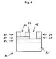
- FIG. 4shows a finished aaPSM made in accordance with the present invention using the photomask blank of FIG. 3 ;
- FIG. 5shows the processing steps used to manufacture an aaPSM in accordance with the present invention
- FIG. 6is a graph showing the effectiveness of MgF x as a substantially transparent etch stop layer in accordance with the present invention.
- FIG. 7shows a blank phase shift mask having a deposited partially transparent layer and a substantially transparent etch stop layer in accordance with the present invention.
- FIG. 8shows a blank photomask having a deposited opaque layer and a substantially transparent etch stop layer in accordance with the present invention.
- the present inventionis directed to an improved aaPSM and method for making the same. More particularly, the present invention utilizes a substantially transparent etch stop layer between a substantially transparent substrate and a deposited substantially transparent layer to insure that a proper opening depth is obtained in the formation of an aaPSM and other photomasks which require etching of substantially transparent substrates.
- the internal substantially transparent etch stop layer of the present inventioncan have additional layers deposited thereon. The internal substantially transparent etch stop layer of the present invention remains on the blank although the additional layers will be removed to form a patterned photomask.
- the characteristics of the internal substantially transparent etch stop layer of the present inventionmay include: (1) imperviousness to dry etch attack; (2) imperviousness to wet etch attack; (3) offering high transmission at desired wavelengths; (4) imperviousness to degradation under exposed radiation conditions; (5) offering an improvement for defect repair integration; (6) capability of being deposited in sufficient thickness as to allow for intensity balancing without undercut for alternating aperture phase shifting applications; (7) imperviousness to absorption of significant radiation at the exposure wavelengths of 157 nm, 193 nm, and or 248 nm; (8) capability of being deposited with either evaporative or sputtered techniques; (9) film properties of excellent adhesion and proper stress balancing; (10) allowing for end point detection during plasma dry etch processing to remove the top layer(s).
- the internal substantially transparent etch stop layer of the present inventionis comprised of MgF 2 deposited under evaporation.
- suitable materialssuch as Al 2 O 3 or Al x N y may also be used as the substantially transparent etch stop layer.
- the blank photomask 31preferably includes five layers, but may include additional layers as needed or desired by the photomask manufacturer.
- the blank photomask 31includes a substantially transparent layer 33 , such as quartz, glass or fused silica.
- the next layeris a substantially transparent etch stop layer 35 .
- the substantially transparent etch stop layer 35is comprised of magnesium fluoride (MgF x ).
- the substantially transparent etch stop layeris comprised of e-beam evaporation of optical quality MgF 2 coatings at ⁇ /4 thickness at 193 nm.
- the next layeris a deposited substantially transparent layer 37 having a thickness of ⁇ /2(n ⁇ 1).
- the deposited substantially transparent layer 37is preferably comprised of SiO 2 , but may be comprised of other materials that are substantially transparent at the exposure wavelengths.
- the next layeris a opaque layer 39 (e.g., chrome) capable of absorbing all (or most) light to which it is exposed.
- the opaque layer 38may additionally include an anti-reflective layer, such as chrome oxide, if desired or needed.
- the next layeris a photosensitive material 41 .
- a pattern defined by an electronic fileis transferred to the blank photomask using conventional lithography tools, including, for example, E-beam and/or laser beam writing tools.
- the laser source which is usedoperates at 365 nm, however, the present invention is not limited to this particular wavelength laser source and will work with a variety of different image sources as discussed herein.
- the blank photomask 31is etched to form an aaPSM 51 having types of transmissive regions: (1) an unetched, film recess 40 covering a corresponding unetched portion of the deposited substantially transparent layer 37 ; and (2) a subtractively etched trench 42 etched in the deposited substantially transparent layer 37 up to the substantially transparent etch stop layer 35 .
- these transmissive regionsalternate between opaque regions on the photomask, as shown in FIG. 4 .
- a pattern in the opaque regions of the photomaskis defined by the following steps.
- the blank photomask of FIG. 3is provided, Step 1 .
- Predefined areas 32 in the photosensitive resist layer 41 of the blank photomask 31are exposed to an energy source (e.g., a light source), Step 2 .
- the exposed photoresist 32is developed (e.g., removed), thereby forming a recess 34 in the photosensitive resist layer 31 , Step 3 .
- the portions of the opaque layer 39 underlying the recesses 34are removed by conventional etching techniques (e.g., dry etching or chemical etching), Step 4 .
- the remaining photosensitive resist 41 overlying the undeveloped portions of the opaque layer 39is removed, thereby exposing portions of the deposited substantially transparent layer 37 underlying the removed portions of the opaque layer 39 , Step 5 .
- the un-etched portions of the opaque layer 33serve to block the exposure light during wafer printing, whereas the portions of the opaque layer which have been etched away define the region of the deposited substantially transparent layer 37 and substantially transparent layer 33 which allows exposure light from the Stepper to pass through.
- the first processing stage of the method of the present inventionis used to form a modified version of a conventional binary photomask by patterning an opaque layer.
- alternating phase-shift featuresare formed in the deposited substantially transparent layer 37 .
- Step 5the remaining portions of the opaque layer 39 and the uncovered portions of the deposited substantially transparent layer are re-coated with photosensitive resist 43 , Step 6 .
- Predefined areas 36 in the photosensitive resist layer 43 of the partially processed photomaskare exposed to an energy source, Step 7 .
- these predefined areaspreferably alternate with the recesses 40 wherein a portion of chrome separates each alternating recess 40 (see Step 10 below) and predefined area.
- the present inventionis not limited to PSMs which have alternating etched regions.
- the exposed areas 36 of the photosensitive resist layer 39are developed (e.g., removed), Step 8 .
- the portions of the deposited substantially transparent layer 39 that are no longer covered by photosensitive resist material 43 (or opaque material 39 )are etched to the substantially transparent etch stop layer 35 , Step 9 .
- the thickness of the deposited substantially transparent layeris chosen to satisfy equation (1).
- a phase shifted, transmissive vertical trench 45is formed in the deposited substantially transparent layer 37 .
- the remaining photoresist 43is removed, Step 10 .
- the resultis an aaPSM having a vertical trench 45 alternating with unetched recess 40 in the deposited substantially transparent layer.
- the method for processing the aaPSM of the present inventionis not limited to the particular processing steps. In this regard, the processing method could be modified so long as the same results are achieved. Additionally, it is noted that the aaPSM of the present invention can be modified to be etched to different depths, in which case more than one substantially transparent etch stop layer and a corresponding number of deposited substantially transparent layers can be used.
- the specified depth and the thickness of substantially transparent layer 33can be selected so that the light that passes through the unetched recess 40 is approximately 180° out of phase from light that passes through the vertical trench 45 , in accordance with the teachings of co-pending U.S. patent application Ser. No. 10/391,001, filed Mar. 18, 2003 to the same assignee, which is hereby incorporated by reference herein.
- aaPSMBy making and using an aaPSM in this manner, there is zero asymmetry between the critical dimensions of the trench 45 and the unetched recess 40 of the deposited substantially transparent layer 37 . As a result, the light intensity transmitted through these regions is balanced.
- Impervious to dry etch attackThe deposited material should have very low and perhaps no noticeable removal in dry plasma etch chemistry containing chlorine and/or fluorine species. Hence, it should as a barrier in the removal of the top layers of the photomask during pattern definition.
- a substantially transparent etch stop layercomprised of MgF 2 deposited under evaporation are impervious to fluorine species using a decoupled plasma source system such as manufactured by Applied Materials, Inc.
- the substantially transparent etch stop layersshould not be removed in sufficient quantity in Inductively Couple Plasma Source, Reactive Ion Etch Sources and similar sources that those skilled in the art may want to apply.
- Impervious to wet etch attackThe deposited material should have very low and perhaps no noticeable removal in wet chemistry containing NH 4 OH and acid based solutions, such as H 2 SO 4 or HCL or other similar chemistries that those skilled in the art should apply.
- the etch stop layershould be made of a material which when deposited should improve the transmission of the photomask above the standard measured transmission by minimizing reflections off the photomask that would be lost from the system. For example, as FIG. 6 shows, when MgF 2 was used as an etch stop layer, the transmission improved by about 3 to 5 percent at the exposure wavelength.
- the optical properties of the materialshould not significantly change under actinic exposures (e.g., 157 nm, 193 nm, and 248 nm). Hence, the transmission remains the same for the lifetime of the photomask during normal use, the optical properties do not change during normal use, the film does not change in any undesired way during normal usage.
- the use of a substantially transparent etch stop layerallows for additional opportunities to repair defects detected in an unwanted area.
- One techniqueis to utilize a focused ion beam (FIB) with XeF 2 chemistry to remove the defect over substantially transparent etch stop layer.
- the substantially transparent etch stop layeracts as protection layer for the underlying substrate so that a phase and or transmission error should not occur during the repair technique.
- One skilled in the artshould be able to repair the substrate using an electron beam or laser beam in similar conditions. Without the substantially transparent etch stop layer, repair work of the defect by further etching would be more difficult since it is likely that there would be a significant change to the optical properties of the photomask rendering it sufficiently deficient or perhaps totally useless for the given application.
- the etch stop layershould be able to provide compensation for the intensity balance one would see in an alternating phase shift application.
- the etch stop layercan act as an attenuator if deposited in the correct thickness in the areas where a trench does not exist. Hence, this eliminates the need for an undercut process which enable very advanced applications such as at the 65 nm node and below that would normally have problems in designing around the undercut requirement and minimum feature width. It allows for smaller geometries on the photomask and hence, smaller geometries on the wafer.
- the material of the etch stop layer of the present inventionshould have a low extinction coefficient (k) at or near zero. Therefore, the transmission through the material is at close to 100% of the exposed wavelength.
- the material of the etch stop layer of the present inventionshould be able to be deposited with known deposition techniques such as sputter deposition, evaporative deposition, chemical vapor deposition, metal organic epitaxy, etc.
- the material of the etch stop layer of the present inventionshould be made to exhibit the proper stress and adhesion to be used in this application.
- the etch stop layerallows for end point detection for dry plasma etch applications, or other etching procedures.
- the substantially transparent etch stop layermay be used in a blank phase shift photomask 60 (e.g., embedded attenuated phase shift photomask (“EAPSM”)) comprising: a photosensitive resist material layer 61 ; an opaque layer 63 underlying said photosensitive resist material layer 61 ; a deposited partially transparent layer 65 underlying the opaque layer 63 ; a substantially transparent etch stop layer 67 underlying the deposited partially transparent layer 65 ; and a substantially transparent substrate 69 underlying the substantially transparent etch stop layer 65 .
- EAPSMembedded attenuated phase shift photomask
- the substantially transparent etch stop layermay be comprised of MgF x
- the substantially transparent etch stop layermay be comprised of Al 2 O 3 or Al x O y , or other similar materials based on the selection criteria discussed above.
- the deposited partially transparent layer 65may be comprised of SiON and the substantially transparent layer (e.g., quartz or fused silica) may be doped with fluorine to facilitate a high transmission of light (e.g., about 85%).
- the blank phase shift photomaskcan be processed as discussed above such that during processing, the etch stop layer will act as an etch stop of the deposited partially transparent layer.
- the substantially transparent etch stop layermay be used in a blank photomask 70 comprising: a photosensitive resist material layer 71 ; an opaque layer 73 underlying said photosensitive resist material layer 71 ; a substantially transparent etch stop layer 75 underlying the opaque layer 73 ; and a substantially transparent substrate 77 underlying the substantially transparent etch stop layer.
- the substantially transparent etch stop layer 75may be comprised of MgF x
- the opaque layer 73is comprised of chrome
- the substantially transparent layer 75is comprised of fused silica. This combination of materials will not impart a phase error or transmission error, thus preventing over etching into the fused silica substrate.
- the substantially transparent etch stop layer 75may be comprised of Al 2 O 3 or Al x O y , or other similar materials based on the selection criteria discussed above.
- the opaque layermay be comprised of tantalum compounds (e.g., Ta, TaN, etc.). These materials etch in fluorine, and thus, when used with an internal substantially transparent etch stop layer (e.g., MgF x ), over etching into the substantially transparent substrate (e.g., fused silica) is prevented.
- the substantially transparent layere.g., quartz or fused silica
- the blank photomaskcan be processed as discussed above or in any other appropriate manner such that during processing, the etch stop layer will act as an etch stop of the opaque layer.
- the etch stop layer of the present inventionmay be used in a wide variety of photomasks.
- the present inventionis not limited to the precise processing steps described herein.
- the aaPSM or other photomasks of the present inventionmay be made with fewer or more processing steps, depending upon the equipment used and needs of the photomask maker.
- the method of the present inventionmay also, for example, form all the unetched regions 40 in a series of processing steps, and form the etched regions 45 in a second series of processing steps.
Landscapes
- Physics & Mathematics (AREA)
- General Physics & Mathematics (AREA)
- Preparing Plates And Mask In Photomechanical Process (AREA)
Abstract
Description
d=λ/2(n−1) (1)
where d is film thickness, n is refractive index at exposure wavelength, λ is exposure wavelength. Thus, it is possible to etch smaller features in a semiconductor wafer and use shorter exposure wavelengths. Since the photoresist layer on the semiconductor wafer (
Claims (35)
Priority Applications (4)
| Application Number | Priority Date | Filing Date | Title |
|---|---|---|---|
| US10/658,039US7049034B2 (en) | 2003-09-09 | 2003-09-09 | Photomask having an internal substantially transparent etch stop layer |
| US10/936,026US20050026053A1 (en) | 2002-08-27 | 2004-09-08 | Photomask having an internal substantially transparent etch stop layer |
| TW093127353ATWI296126B (en) | 2003-09-09 | 2004-09-09 | Photomask having an internal substantially transparent etch stop layer |
| PCT/US2004/029452WO2005036264A2 (en) | 2003-09-09 | 2004-09-09 | Photomask having an internal substantially transparent etch stop layer |
Applications Claiming Priority (1)
| Application Number | Priority Date | Filing Date | Title |
|---|---|---|---|
| US10/658,039US7049034B2 (en) | 2003-09-09 | 2003-09-09 | Photomask having an internal substantially transparent etch stop layer |
Related Child Applications (1)
| Application Number | Title | Priority Date | Filing Date |
|---|---|---|---|
| US10/936,026Continuation-In-PartUS20050026053A1 (en) | 2002-08-27 | 2004-09-08 | Photomask having an internal substantially transparent etch stop layer |
Publications (2)
| Publication Number | Publication Date |
|---|---|
| US20050053847A1 US20050053847A1 (en) | 2005-03-10 |
| US7049034B2true US7049034B2 (en) | 2006-05-23 |
Family
ID=34226700
Family Applications (1)
| Application Number | Title | Priority Date | Filing Date |
|---|---|---|---|
| US10/658,039Expired - LifetimeUS7049034B2 (en) | 2002-08-27 | 2003-09-09 | Photomask having an internal substantially transparent etch stop layer |
Country Status (2)
| Country | Link |
|---|---|
| US (1) | US7049034B2 (en) |
| TW (1) | TWI296126B (en) |
Cited By (4)
| Publication number | Priority date | Publication date | Assignee | Title |
|---|---|---|---|---|
| US20110159415A1 (en)* | 2009-12-30 | 2011-06-30 | Hynix Semiconductor Inc. | Etching apparatus and method for fabricating alternating phase shift mask using the same |
| US20110159414A1 (en)* | 2009-12-30 | 2011-06-30 | Hynix Semiconductor Inc. | Method and system of fabricating alternating phase shift mask |
| US8465885B2 (en) | 2011-02-07 | 2013-06-18 | International Business Machines Corporation | Boundary layer formation and resultant structures |
| US9646847B2 (en) | 2013-12-20 | 2017-05-09 | Boe Technology Group Co., Ltd. | Method for manufacturing array substrate, film-etching monitoring method and device |
Families Citing this family (6)
| Publication number | Priority date | Publication date | Assignee | Title |
|---|---|---|---|---|
| JP2004264415A (en)* | 2003-02-28 | 2004-09-24 | Pioneer Electronic Corp | Electron beam recording board |
| US8900469B2 (en)* | 2011-12-19 | 2014-12-02 | Applied Materials, Inc. | Etch rate detection for anti-reflective coating layer and absorber layer etching |
| CN104335117B (en)* | 2012-06-04 | 2016-09-07 | 应用材料公司 | optical projection array exposure system |
| US9921467B2 (en)* | 2015-11-30 | 2018-03-20 | Taiwan Semiconductor Manufacturing Company Ltd. | Mask blank and mask and fabrication method thereof |
| US10816891B2 (en) | 2016-12-14 | 2020-10-27 | Taiwan Semiconductor Manufacturing Company, Ltd. | Photomask and fabrication method therefor |
| US10859905B2 (en) | 2018-09-18 | 2020-12-08 | Taiwan Semiconductor Manufacturing Company Ltd. | Photomask and method for forming the same |
Citations (59)
| Publication number | Priority date | Publication date | Assignee | Title |
|---|---|---|---|---|
| US4178403A (en) | 1977-08-04 | 1979-12-11 | Konishiroku Photo Industry Co., Ltd. | Mask blank and mask |
| US4556608A (en) | 1980-10-09 | 1985-12-03 | Dai Nippon Insatsu Kabushiki Kaisha | Photomask blank and photomask |
| US4720442A (en) | 1985-05-28 | 1988-01-19 | Asahi Glass Company Ltd. | Photomask blank and photomask |
| JPH0239153A (en) | 1988-07-29 | 1990-02-08 | Toppan Printing Co Ltd | Photomask blank and photomask |
| JPH07104457A (en) | 1993-08-13 | 1995-04-21 | Toshiba Corp | Exposure mask, manufacturing method and manufacturing apparatus therefor |
| US5439763A (en) | 1991-03-19 | 1995-08-08 | Hitachi, Ltd. | Optical mask and method of correcting the same |
| US5451543A (en) | 1994-04-25 | 1995-09-19 | Motorola, Inc. | Straight sidewall profile contact opening to underlying interconnect and method for making the same |
| US5460908A (en) | 1991-08-02 | 1995-10-24 | Micron Technology, Inc. | Phase shifting retical fabrication method |
| US5472811A (en) | 1993-01-21 | 1995-12-05 | Sematech, Inc. | Phase shifting mask structure with multilayer optical coating for improved transmission |
| US5477058A (en) | 1994-11-09 | 1995-12-19 | Kabushiki Kaisha Toshiba | Attenuated phase-shifting mask with opaque reticle alignment marks |
| US5482799A (en) | 1993-10-08 | 1996-01-09 | Mitsubishi Denki Kabushiki Kaisha | Phase shift mask and manufacturing method thereof |
| JPH0876353A (en) | 1994-09-08 | 1996-03-22 | Nec Corp | Production of phase shift mask |
| US5547787A (en) | 1992-04-22 | 1996-08-20 | Kabushiki Kaisha Toshiba | Exposure mask, exposure mask substrate, method for fabricating the same, and method for forming pattern based on exposure mask |
| US5578402A (en) | 1990-06-21 | 1996-11-26 | Matsushita Electronics Corporation | Photomask used by photolithography and a process of producing same |
| US5693568A (en) | 1995-12-14 | 1997-12-02 | Advanced Micro Devices, Inc. | Reverse damascene via structures |
| US5725973A (en) | 1994-02-07 | 1998-03-10 | Samsung Electronic Co., Ltd. | Photo mask and method for manufacturing same |
| US5756396A (en) | 1996-05-06 | 1998-05-26 | Taiwan Semiconductor Manufacturing Company Ltd | Method of making a multi-layer wiring structure having conductive sidewall etch stoppers and a stacked plug interconnect |
| US5876877A (en)* | 1990-12-28 | 1999-03-02 | Fujitsu Limited | Patterned mask having a transparent etching stopper layer |
| US5935740A (en) | 1996-12-09 | 1999-08-10 | Micron Technology, Inc. | Method and apparatus for the fabrication of semiconductor photomask |
| US5935733A (en) | 1996-04-05 | 1999-08-10 | Intel Corporation | Photolithography mask and method of fabrication |
| US5939227A (en) | 1998-03-09 | 1999-08-17 | Rochester Institute Of Technology | Multi-layered attenuated phase shift mask and a method for making the mask |
| US5955222A (en) | 1996-12-03 | 1999-09-21 | International Business Machines Corporation | Method of making a rim-type phase-shift mask and mask manufactured thereby |
| US5981110A (en) | 1998-02-17 | 1999-11-09 | International Business Machines Corporation | Method for repairing photomasks |
| US6120942A (en) | 1997-02-18 | 2000-09-19 | Micron Technology, Inc. | Method for making a photomask with multiple absorption levels |
| US6174771B1 (en) | 1998-11-17 | 2001-01-16 | Winbond Electronics Corp. | Split gate flash memory cell with self-aligned process |
| US6187480B1 (en) | 1998-04-03 | 2001-02-13 | United Microelectronics Corp. | Alternating phase-shifting mask |
| US6190836B1 (en) | 1997-01-21 | 2001-02-20 | International Business Machines Corporation | Methods for repair of photomasks |
| JP2001174973A (en) | 1999-12-15 | 2001-06-29 | Dainippon Printing Co Ltd | Halftone phase shift photomask and blank for halftone phase shift photomask |
| US6261963B1 (en) | 2000-07-07 | 2001-07-17 | Advanced Micro Devices, Inc. | Reverse electroplating of barrier metal layer to improve electromigration performance in copper interconnect devices |
| US20010035547A1 (en) | 2000-04-27 | 2001-11-01 | Nec Corporation | Semiconductor device and method of fabricating same |
| US20010044056A1 (en) | 2000-05-17 | 2001-11-22 | Haruo Kokubo | Phase-shift photomask manufacturing method and phase-shift photomask |
| US20010051420A1 (en) | 2000-01-19 | 2001-12-13 | Besser Paul R. | Dielectric formation to seal porosity of low dielectic constant (low k) materials after etch |
| US6335130B1 (en) | 2000-05-01 | 2002-01-01 | Asml Masktools Netherlands B.V. | System and method of providing optical proximity correction for features using phase-shifted halftone transparent/semi-transparent features |
| US6355557B2 (en) | 1998-07-22 | 2002-03-12 | Applied Materials, Inc. | Oxide plasma etching process with a controlled wineglass shape |
| US6368967B1 (en) | 2000-05-04 | 2002-04-09 | Advanced Micro Devices, Inc. | Method to control mechanical stress of copper interconnect line using post-plating copper anneal |
| US6429033B1 (en) | 2001-02-20 | 2002-08-06 | Nayna Networks, Inc. | Process for manufacturing mirror devices using semiconductor technology |
| US20020111030A1 (en) | 1998-12-17 | 2002-08-15 | Shubneesh Batra | Stepped photoresist profile and opening formed using the profile |
| US20020123217A1 (en) | 2000-12-05 | 2002-09-05 | Ramkumar Subramanian | Damascene processing employing low si-sion etch stop layer/arc |
| US20020142585A1 (en) | 2000-01-18 | 2002-10-03 | Applied Materials, Inc. | Very low dielectric constant plasma-enhanced CVD films |
| US20020160520A1 (en) | 2001-03-16 | 2002-10-31 | Phoenix Bioscience | Silicon nano-collection analytic device |
| US20020173162A1 (en) | 2000-03-10 | 2002-11-21 | Jingbao Liu | Magnetically enhanced plasma oxide etch using hexafluorobutadiene |
| US20020192944A1 (en) | 2001-06-13 | 2002-12-19 | Sonderman Thomas J. | Method and apparatus for controlling a thickness of a copper film |
| US6515343B1 (en) | 1998-11-19 | 2003-02-04 | Quicklogic Corporation | Metal-to-metal antifuse with non-conductive diffusion barrier |
| US6544696B2 (en) | 2000-12-01 | 2003-04-08 | Unaxis Usa Inc. | Embedded attenuated phase shift mask and method of making embedded attenuated phase shift mask |
| US6562522B1 (en) | 1999-10-29 | 2003-05-13 | Intel Corporation | Photomasking |
| US6582856B1 (en)* | 2000-02-28 | 2003-06-24 | Chartered Semiconductor Manufacturing Ltd. | Simplified method of fabricating a rim phase shift mask |
| US20030118920A1 (en) | 2001-12-13 | 2003-06-26 | Dupont Photomasks, Inc. | Multi-tone photomask and method for manufacturing the same |
| US6610594B2 (en) | 2001-07-10 | 2003-08-26 | Advanced Micro Devices, Inc. | Locally increasing sidewall density by ion implantation |
| US20030228047A1 (en) | 2002-06-07 | 2003-12-11 | Taiwan Semiconductor Manufacturing Co., Ltd. | Photomask transparent substrate protection during removal of opaque photomask defects |
| US20030228529A1 (en) | 2002-06-10 | 2003-12-11 | Dupont Photomasks, Inc. | Photomask and method for repairing defects |
| US6699625B2 (en) | 2000-10-13 | 2004-03-02 | Samsung Electronics Co., Ltd. | Reflection photomasks including buffer layer comprising group VIII metal, and methods of fabricating and using the same |
| US6703252B2 (en) | 2002-01-31 | 2004-03-09 | Hewlett-Packard Development Company, L.P. | Method of manufacturing an emitter |
| US20040058139A1 (en) | 2002-09-23 | 2004-03-25 | Dubin Valery M. | Seed layer treatment |
| US6730445B2 (en) | 2002-04-12 | 2004-05-04 | International Business Machines Corporation | Attenuated embedded phase shift photomask blanks |
| US20040094760A1 (en) | 2002-10-25 | 2004-05-20 | The University Of Connecticut | Optoelectronic circuit employing a heterojunction thyristor device to convert a digital optical signal to a digital electrical signal |
| US6743553B2 (en) | 2000-12-26 | 2004-06-01 | Hoya Corporation | Halftone phase shift mask and mask blank |
| US20040126057A1 (en) | 2002-01-16 | 2004-07-01 | Yoo Sung-Joo Ben | Optical routing method |
| US20040137335A1 (en) | 2003-01-14 | 2004-07-15 | Asml Netherlands B.V. | Embedded etch stop for phase shift masks and planar phase shift masks to reduce topography induced and wave guide effects |
| US6780548B1 (en) | 2001-01-11 | 2004-08-24 | Dupont Photomasks, Inc. | Alternating aperture phase shifting photomask with improved transmission balancing |
Family Cites Families (1)
| Publication number | Priority date | Publication date | Assignee | Title |
|---|---|---|---|---|
| US5965936A (en)* | 1997-12-31 | 1999-10-12 | Micron Technology, Inc. | Multi-layer lead frame for a semiconductor device |
- 2003
- 2003-09-09USUS10/658,039patent/US7049034B2/ennot_activeExpired - Lifetime
- 2004
- 2004-09-09TWTW093127353Apatent/TWI296126B/ennot_activeIP Right Cessation
Patent Citations (61)
| Publication number | Priority date | Publication date | Assignee | Title |
|---|---|---|---|---|
| US4178403A (en) | 1977-08-04 | 1979-12-11 | Konishiroku Photo Industry Co., Ltd. | Mask blank and mask |
| US4556608A (en) | 1980-10-09 | 1985-12-03 | Dai Nippon Insatsu Kabushiki Kaisha | Photomask blank and photomask |
| US4720442A (en) | 1985-05-28 | 1988-01-19 | Asahi Glass Company Ltd. | Photomask blank and photomask |
| JPH0239153A (en) | 1988-07-29 | 1990-02-08 | Toppan Printing Co Ltd | Photomask blank and photomask |
| US5578402A (en) | 1990-06-21 | 1996-11-26 | Matsushita Electronics Corporation | Photomask used by photolithography and a process of producing same |
| US5876877A (en)* | 1990-12-28 | 1999-03-02 | Fujitsu Limited | Patterned mask having a transparent etching stopper layer |
| US5439763A (en) | 1991-03-19 | 1995-08-08 | Hitachi, Ltd. | Optical mask and method of correcting the same |
| US5460908A (en) | 1991-08-02 | 1995-10-24 | Micron Technology, Inc. | Phase shifting retical fabrication method |
| US5547787A (en) | 1992-04-22 | 1996-08-20 | Kabushiki Kaisha Toshiba | Exposure mask, exposure mask substrate, method for fabricating the same, and method for forming pattern based on exposure mask |
| US5472811A (en) | 1993-01-21 | 1995-12-05 | Sematech, Inc. | Phase shifting mask structure with multilayer optical coating for improved transmission |
| JPH07104457A (en) | 1993-08-13 | 1995-04-21 | Toshiba Corp | Exposure mask, manufacturing method and manufacturing apparatus therefor |
| US5482799A (en) | 1993-10-08 | 1996-01-09 | Mitsubishi Denki Kabushiki Kaisha | Phase shift mask and manufacturing method thereof |
| US5725973A (en) | 1994-02-07 | 1998-03-10 | Samsung Electronic Co., Ltd. | Photo mask and method for manufacturing same |
| US5451543A (en) | 1994-04-25 | 1995-09-19 | Motorola, Inc. | Straight sidewall profile contact opening to underlying interconnect and method for making the same |
| JPH0876353A (en) | 1994-09-08 | 1996-03-22 | Nec Corp | Production of phase shift mask |
| US5477058A (en) | 1994-11-09 | 1995-12-19 | Kabushiki Kaisha Toshiba | Attenuated phase-shifting mask with opaque reticle alignment marks |
| US5693568A (en) | 1995-12-14 | 1997-12-02 | Advanced Micro Devices, Inc. | Reverse damascene via structures |
| US5935733A (en) | 1996-04-05 | 1999-08-10 | Intel Corporation | Photolithography mask and method of fabrication |
| US5756396A (en) | 1996-05-06 | 1998-05-26 | Taiwan Semiconductor Manufacturing Company Ltd | Method of making a multi-layer wiring structure having conductive sidewall etch stoppers and a stacked plug interconnect |
| US5955222A (en) | 1996-12-03 | 1999-09-21 | International Business Machines Corporation | Method of making a rim-type phase-shift mask and mask manufactured thereby |
| US5935740A (en) | 1996-12-09 | 1999-08-10 | Micron Technology, Inc. | Method and apparatus for the fabrication of semiconductor photomask |
| US6190836B1 (en) | 1997-01-21 | 2001-02-20 | International Business Machines Corporation | Methods for repair of photomasks |
| US6120942A (en) | 1997-02-18 | 2000-09-19 | Micron Technology, Inc. | Method for making a photomask with multiple absorption levels |
| US6221542B1 (en) | 1997-02-18 | 2001-04-24 | Micron Technology, Inc. | Method for patterning a substrate using a photomask with multiple absorption levels |
| US5981110A (en) | 1998-02-17 | 1999-11-09 | International Business Machines Corporation | Method for repairing photomasks |
| US5939227A (en) | 1998-03-09 | 1999-08-17 | Rochester Institute Of Technology | Multi-layered attenuated phase shift mask and a method for making the mask |
| US6187480B1 (en) | 1998-04-03 | 2001-02-13 | United Microelectronics Corp. | Alternating phase-shifting mask |
| US6355557B2 (en) | 1998-07-22 | 2002-03-12 | Applied Materials, Inc. | Oxide plasma etching process with a controlled wineglass shape |
| US6174771B1 (en) | 1998-11-17 | 2001-01-16 | Winbond Electronics Corp. | Split gate flash memory cell with self-aligned process |
| US6515343B1 (en) | 1998-11-19 | 2003-02-04 | Quicklogic Corporation | Metal-to-metal antifuse with non-conductive diffusion barrier |
| US20020111030A1 (en) | 1998-12-17 | 2002-08-15 | Shubneesh Batra | Stepped photoresist profile and opening formed using the profile |
| US6562522B1 (en) | 1999-10-29 | 2003-05-13 | Intel Corporation | Photomasking |
| JP2001174973A (en) | 1999-12-15 | 2001-06-29 | Dainippon Printing Co Ltd | Halftone phase shift photomask and blank for halftone phase shift photomask |
| US20030211728A1 (en) | 2000-01-18 | 2003-11-13 | Applied Materials, Inc. | Very low dielectric constant plasma-enhanced CVD films |
| US20020142585A1 (en) | 2000-01-18 | 2002-10-03 | Applied Materials, Inc. | Very low dielectric constant plasma-enhanced CVD films |
| US20010051420A1 (en) | 2000-01-19 | 2001-12-13 | Besser Paul R. | Dielectric formation to seal porosity of low dielectic constant (low k) materials after etch |
| US6582856B1 (en)* | 2000-02-28 | 2003-06-24 | Chartered Semiconductor Manufacturing Ltd. | Simplified method of fabricating a rim phase shift mask |
| US20020173162A1 (en) | 2000-03-10 | 2002-11-21 | Jingbao Liu | Magnetically enhanced plasma oxide etch using hexafluorobutadiene |
| US20010035547A1 (en) | 2000-04-27 | 2001-11-01 | Nec Corporation | Semiconductor device and method of fabricating same |
| US6335130B1 (en) | 2000-05-01 | 2002-01-01 | Asml Masktools Netherlands B.V. | System and method of providing optical proximity correction for features using phase-shifted halftone transparent/semi-transparent features |
| US6368967B1 (en) | 2000-05-04 | 2002-04-09 | Advanced Micro Devices, Inc. | Method to control mechanical stress of copper interconnect line using post-plating copper anneal |
| US20010044056A1 (en) | 2000-05-17 | 2001-11-22 | Haruo Kokubo | Phase-shift photomask manufacturing method and phase-shift photomask |
| US6261963B1 (en) | 2000-07-07 | 2001-07-17 | Advanced Micro Devices, Inc. | Reverse electroplating of barrier metal layer to improve electromigration performance in copper interconnect devices |
| US6699625B2 (en) | 2000-10-13 | 2004-03-02 | Samsung Electronics Co., Ltd. | Reflection photomasks including buffer layer comprising group VIII metal, and methods of fabricating and using the same |
| US6544696B2 (en) | 2000-12-01 | 2003-04-08 | Unaxis Usa Inc. | Embedded attenuated phase shift mask and method of making embedded attenuated phase shift mask |
| US20020123217A1 (en) | 2000-12-05 | 2002-09-05 | Ramkumar Subramanian | Damascene processing employing low si-sion etch stop layer/arc |
| US6743553B2 (en) | 2000-12-26 | 2004-06-01 | Hoya Corporation | Halftone phase shift mask and mask blank |
| US6780548B1 (en) | 2001-01-11 | 2004-08-24 | Dupont Photomasks, Inc. | Alternating aperture phase shifting photomask with improved transmission balancing |
| US6429033B1 (en) | 2001-02-20 | 2002-08-06 | Nayna Networks, Inc. | Process for manufacturing mirror devices using semiconductor technology |
| US20020160520A1 (en) | 2001-03-16 | 2002-10-31 | Phoenix Bioscience | Silicon nano-collection analytic device |
| US20020192944A1 (en) | 2001-06-13 | 2002-12-19 | Sonderman Thomas J. | Method and apparatus for controlling a thickness of a copper film |
| US6610594B2 (en) | 2001-07-10 | 2003-08-26 | Advanced Micro Devices, Inc. | Locally increasing sidewall density by ion implantation |
| US20030118920A1 (en) | 2001-12-13 | 2003-06-26 | Dupont Photomasks, Inc. | Multi-tone photomask and method for manufacturing the same |
| US20040126057A1 (en) | 2002-01-16 | 2004-07-01 | Yoo Sung-Joo Ben | Optical routing method |
| US6703252B2 (en) | 2002-01-31 | 2004-03-09 | Hewlett-Packard Development Company, L.P. | Method of manufacturing an emitter |
| US6730445B2 (en) | 2002-04-12 | 2004-05-04 | International Business Machines Corporation | Attenuated embedded phase shift photomask blanks |
| US20030228047A1 (en) | 2002-06-07 | 2003-12-11 | Taiwan Semiconductor Manufacturing Co., Ltd. | Photomask transparent substrate protection during removal of opaque photomask defects |
| US20030228529A1 (en) | 2002-06-10 | 2003-12-11 | Dupont Photomasks, Inc. | Photomask and method for repairing defects |
| US20040058139A1 (en) | 2002-09-23 | 2004-03-25 | Dubin Valery M. | Seed layer treatment |
| US20040094760A1 (en) | 2002-10-25 | 2004-05-20 | The University Of Connecticut | Optoelectronic circuit employing a heterojunction thyristor device to convert a digital optical signal to a digital electrical signal |
| US20040137335A1 (en) | 2003-01-14 | 2004-07-15 | Asml Netherlands B.V. | Embedded etch stop for phase shift masks and planar phase shift masks to reduce topography induced and wave guide effects |
Non-Patent Citations (12)
| Title |
|---|
| Armin Semmler, L. Mader, A. Elsner, R. Koehle, O. Griesinger, C. Noelscher "Application of 3D EMF Simulation for Development and Optimization of Alternating Phase Shifting Masks", Optical Microlithography XIV, Proceedings of SPIE, 2001, p. 356-367, vol. 4346 (Christopher J. Progler, ed.). |
| Canon Presentation, "Canon's IDEAL: Innovative Double Exposure by Advanced Lithography," BACUS News, SPIE, Apr. 2001, vol. 17, Issue 4, p. 1-7. |
| K.D. Lucas, C.M. Yuan, and A.J. Stroljwas, "A rigorous and practical vector model for phase shigting masks in optical lithography", Proc. SPIE 1674, 252-263 (1992). |
| M.D. Levenson, N.S. Viswanathan, and R.A. Simpson, "Improving Resolution with a Phase-Shifting Mask", IEEE Trans. Elect. Dev. ED-29, 1828-1836 (1982.) |
| Matthew Lassiter, et al., "157nm Binary and Embedded Attenuated PSM Films", 157 nm Symposium, Yokohama (2003). |
| Matthew Lassiter, et al., "Improved Phase Uniformity Control Using a New AAPSM Etch Stop Layer Technique", SPIE vol. 5256, 23rd Annual BACUS Symposium on Photomask Technology (2003). |
| Michael Cangemi, et al., "Implementation of a Transparent Etch Stop Layer for an Improved Alternating PSM", VDE vol. 43, 20th European Conference on Mask Technology for Integrated Circuits and Microcomponents 2004. |
| R.L. Kosetelak, C. Pierrat, J.G. Garofalo, and S. Vaidya, "Exposure characteristics of alternate aperture phase-shifting masks fabricated using a subtractive process", J. Vac. Sci. Tech. B0, 3055-3061 (1992). |
| Song Peng, "Through-Focus Image Balancing of Alternating Phase Shifting Maskes", SPIE vol. 3873, p. 328-336 (1999). |
| T. Ebihara, T. Oga, P.D. Rhyins, M. Sweis, P.M. Martin, "150-nm dense/isolated contact hole study with Canon IDEAL technique", SPIE Proceeding 4562-119. |
| T. Terasawa, N. Hasegawa, A. IMAI and S. Okazaki, "Analysis of Nonplanar Topography Effects of Phase Shift Masks on Imaging Characteristics", Japanese J. Appl. Phys. 34, 6578-6583 (1995). |
| T. Teresawa, N, Hasegawa, T. Tanaka, S. Katagiri, and T. Kurosaki, "Improved Resolution of an i-line stepper using a phase-shift mask", J. Vac. Sci. Tech. B8, 1300-1308, (1990). |
Cited By (5)
| Publication number | Priority date | Publication date | Assignee | Title |
|---|---|---|---|---|
| US20110159415A1 (en)* | 2009-12-30 | 2011-06-30 | Hynix Semiconductor Inc. | Etching apparatus and method for fabricating alternating phase shift mask using the same |
| US20110159414A1 (en)* | 2009-12-30 | 2011-06-30 | Hynix Semiconductor Inc. | Method and system of fabricating alternating phase shift mask |
| US8470499B2 (en) | 2009-12-30 | 2013-06-25 | SK Hynix Inc. | Method and system of fabricating alternating phase shift mask |
| US8465885B2 (en) | 2011-02-07 | 2013-06-18 | International Business Machines Corporation | Boundary layer formation and resultant structures |
| US9646847B2 (en) | 2013-12-20 | 2017-05-09 | Boe Technology Group Co., Ltd. | Method for manufacturing array substrate, film-etching monitoring method and device |
Also Published As
| Publication number | Publication date |
|---|---|
| US20050053847A1 (en) | 2005-03-10 |
| TWI296126B (en) | 2008-04-21 |
| TW200514135A (en) | 2005-04-16 |
Similar Documents
| Publication | Publication Date | Title |
|---|---|---|
| US5582939A (en) | Method for fabricating and using defect-free phase shifting masks | |
| EP0674223B1 (en) | An attenuating phase-shift mask structure and fabrication method | |
| KR100758052B1 (en) | Phase Shift Photo Mask and Phase Shift Photo Mask Dry Etching Method | |
| TW535211B (en) | Transmission and phase balance for phase-shifting mask | |
| KR100425903B1 (en) | Pattern shape evaluation method in photomask, photomask, photomask production method, photomask pattern formation method, and exposure method | |
| EP0838726A1 (en) | Halftone phase shift mask, blank for the same, and methods of manufacturing these | |
| US7906252B2 (en) | Multiple resist layer phase shift mask (PSM) blank and PSM formation method | |
| US10670956B2 (en) | Photomask having a plurality of shielding layers | |
| US20060051681A1 (en) | Method of repairing a photomask having an internal etch stop layer | |
| TWI388922B (en) | Pattern forming method and method of manufacturing phase shift mask | |
| US5380608A (en) | Phase shift photomask comprising a layer of aluminum oxide with magnesium oxide | |
| US8563227B2 (en) | Method and system for exposure of a phase shift mask | |
| US7049034B2 (en) | Photomask having an internal substantially transparent etch stop layer | |
| EP1321820A1 (en) | Halftone phase shift photomask and blank for halftone phase shift photomask | |
| CN101006329A (en) | Embedded attenuated phase shift mask with tunable transmission | |
| US7008735B2 (en) | Mask for improving lithography performance by using multi-transmittance photomask | |
| US6933084B2 (en) | Alternating aperture phase shift photomask having light absorption layer | |
| US20050026053A1 (en) | Photomask having an internal substantially transparent etch stop layer | |
| US20040086787A1 (en) | Alternating aperture phase shift photomask having plasma etched isotropic quartz features | |
| US6660436B1 (en) | OPC-like repair method for attenuated phase shift masks | |
| KR20040010870A (en) | Photomask for forming small contact holes array, method for fabricating the same and method for using the same | |
| JPH08123008A (en) | Phase shift mask and manufacturing method thereof | |
| US6780548B1 (en) | Alternating aperture phase shifting photomask with improved transmission balancing | |
| WO2005103820A1 (en) | Levenson type phase shift mask and production method therefor | |
| US6924069B2 (en) | Method for repairing attenuated phase shift masks |
Legal Events
| Date | Code | Title | Description |
|---|---|---|---|
| AS | Assignment | Owner name:PHOTRONICS, INC., CONNECTICUT Free format text:ASSIGNMENT OF ASSIGNORS INTEREST;ASSIGNORS:MARTIN, PATRICK M.;LASSITER, MATTHEW;TAYLOR, DARREN;AND OTHERS;REEL/FRAME:015122/0491;SIGNING DATES FROM 20040123 TO 20040204 | |
| STCF | Information on status: patent grant | Free format text:PATENTED CASE | |
| AS | Assignment | Owner name:JPMORGAN CHASE BANK, NATIONAL ASSOCIATION, ILLINOI Free format text:SECURITY AGREEMENT;ASSIGNOR:PHOTRONICS, INC.;REEL/FRAME:021976/0635 Effective date:20081212 Owner name:JPMORGAN CHASE BANK, NATIONAL ASSOCIATION,ILLINOIS Free format text:SECURITY AGREEMENT;ASSIGNOR:PHOTRONICS, INC.;REEL/FRAME:021976/0635 Effective date:20081212 | |
| AS | Assignment | Owner name:JPMORGAN CHASE BANK, NATIONAL ASSOCIATION, ILLINOI Free format text:SECURITY AGREEMENT;ASSIGNOR:PHOTRONICS, INC.;REEL/FRAME:022012/0009 Effective date:20081212 Owner name:JPMORGAN CHASE BANK, NATIONAL ASSOCIATION,ILLINOIS Free format text:SECURITY AGREEMENT;ASSIGNOR:PHOTRONICS, INC.;REEL/FRAME:022012/0009 Effective date:20081212 | |
| FPAY | Fee payment | Year of fee payment:4 | |
| AS | Assignment | Owner name:JPMORGAN CHASE BANK, N.A., AS COLLATERAL AGENT,ILL Free format text:SECURITY AGREEMENT;ASSIGNOR:PHOTRONICS, INC.;REEL/FRAME:023928/0612 Effective date:20100212 Owner name:JPMORGAN CHASE BANK, N.A., AS COLLATERAL AGENT, IL Free format text:SECURITY AGREEMENT;ASSIGNOR:PHOTRONICS, INC.;REEL/FRAME:023928/0612 Effective date:20100212 | |
| FPAY | Fee payment | Year of fee payment:8 | |
| MAFP | Maintenance fee payment | Free format text:PAYMENT OF MAINTENANCE FEE, 12TH YEAR, LARGE ENTITY (ORIGINAL EVENT CODE: M1553) Year of fee payment:12 | |
| AS | Assignment | Owner name:JPMORGAN CHASE BANK, N.A., AS COLLATERAL AGENT, ILLINOIS Free format text:SECURITY INTEREST;ASSIGNOR:PHOTRONICS, INC.;REEL/FRAME:047002/0633 Effective date:20180927 Owner name:JPMORGAN CHASE BANK, N.A., AS COLLATERAL AGENT, IL Free format text:SECURITY INTEREST;ASSIGNOR:PHOTRONICS, INC.;REEL/FRAME:047002/0633 Effective date:20180927 |