US7046022B2 - Assembly for electrically connecting a test component to a testing machine for testing electrical circuits on the test component - Google Patents
Assembly for electrically connecting a test component to a testing machine for testing electrical circuits on the test componentDownload PDFInfo
- Publication number
- US7046022B2 US7046022B2US10/912,785US91278504AUS7046022B2US 7046022 B2US7046022 B2US 7046022B2US 91278504 AUS91278504 AUS 91278504AUS 7046022 B2US7046022 B2US 7046022B2
- Authority
- US
- United States
- Prior art keywords
- electrical
- contactor
- assembly
- test component
- interposer
- Prior art date
- Legal status (The legal status is an assumption and is not a legal conclusion. Google has not performed a legal analysis and makes no representation as to the accuracy of the status listed.)
- Expired - Lifetime, expires
Links
- 238000012360testing methodMethods0.000titleclaimsabstractdescription42
- 239000000758substrateSubstances0.000claimsdescription15
- 239000004020conductorSubstances0.000claimsdescription10
- PCHJSUWPFVWCPO-UHFFFAOYSA-NgoldChemical compound[Au]PCHJSUWPFVWCPO-UHFFFAOYSA-N0.000claimsdescription5
- 239000010931goldSubstances0.000claimsdescription5
- 229910052737goldInorganic materials0.000claimsdescription5
- 239000000523sampleSubstances0.000abstractdescription23
- 238000010586diagramMethods0.000description12
- 239000002184metalSubstances0.000description8
- 229910052751metalInorganic materials0.000description8
- 238000006073displacement reactionMethods0.000description6
- 230000015572biosynthetic processEffects0.000description4
- 239000000463materialSubstances0.000description4
- 230000000295complement effectEffects0.000description3
- 230000008878couplingEffects0.000description3
- 238000010168coupling processMethods0.000description3
- 238000005859coupling reactionMethods0.000description3
- 230000006835compressionEffects0.000description2
- 238000007906compressionMethods0.000description2
- NJPPVKZQTLUDBO-UHFFFAOYSA-NnovaluronChemical compoundC1=C(Cl)C(OC(F)(F)C(OC(F)(F)F)F)=CC=C1NC(=O)NC(=O)C1=C(F)C=CC=C1FNJPPVKZQTLUDBO-UHFFFAOYSA-N0.000description2
- 239000004642PolyimideSubstances0.000description1
- 238000006243chemical reactionMethods0.000description1
- 230000002950deficientEffects0.000description1
- 230000000694effectsEffects0.000description1
- 239000012530fluidSubstances0.000description1
- 238000004519manufacturing processMethods0.000description1
- 230000015654memoryEffects0.000description1
- 238000000034methodMethods0.000description1
- 230000004048modificationEffects0.000description1
- 238000012986modificationMethods0.000description1
- 239000004033plasticSubstances0.000description1
- 229920001721polyimidePolymers0.000description1
- 239000012858resilient materialSubstances0.000description1
Images


Classifications
- G—PHYSICS
- G01—MEASURING; TESTING
- G01R—MEASURING ELECTRIC VARIABLES; MEASURING MAGNETIC VARIABLES
- G01R1/00—Details of instruments or arrangements of the types included in groups G01R5/00 - G01R13/00 and G01R31/00
- G01R1/02—General constructional details
- G01R1/04—Housings; Supporting members; Arrangements of terminals
- G01R1/0408—Test fixtures or contact fields; Connectors or connecting adaptors; Test clips; Test sockets
- G01R1/0491—Test fixtures or contact fields; Connectors or connecting adaptors; Test clips; Test sockets for testing integrated circuits on wafers, e.g. wafer-level test cartridge
- G—PHYSICS
- G01—MEASURING; TESTING
- G01R—MEASURING ELECTRIC VARIABLES; MEASURING MAGNETIC VARIABLES
- G01R1/00—Details of instruments or arrangements of the types included in groups G01R5/00 - G01R13/00 and G01R31/00
- G01R1/02—General constructional details
- G01R1/06—Measuring leads; Measuring probes
- G01R1/067—Measuring probes
- G01R1/073—Multiple probes
- G01R1/07307—Multiple probes with individual probe elements, e.g. needles, cantilever beams or bump contacts, fixed in relation to each other, e.g. bed of nails fixture or probe card
- G01R1/07364—Multiple probes with individual probe elements, e.g. needles, cantilever beams or bump contacts, fixed in relation to each other, e.g. bed of nails fixture or probe card with provisions for altering position, number or connection of probe tips; Adapting to differences in pitch
- G01R1/07378—Multiple probes with individual probe elements, e.g. needles, cantilever beams or bump contacts, fixed in relation to each other, e.g. bed of nails fixture or probe card with provisions for altering position, number or connection of probe tips; Adapting to differences in pitch using an intermediate adapter, e.g. space transformers
- G—PHYSICS
- G01—MEASURING; TESTING
- G01R—MEASURING ELECTRIC VARIABLES; MEASURING MAGNETIC VARIABLES
- G01R31/00—Arrangements for testing electric properties; Arrangements for locating electric faults; Arrangements for electrical testing characterised by what is being tested not provided for elsewhere
- G01R31/28—Testing of electronic circuits, e.g. by signal tracer
- G01R31/2851—Testing of integrated circuits [IC]
- G01R31/2855—Environmental, reliability or burn-in testing
- G01R31/286—External aspects, e.g. related to chambers, contacting devices or handlers
- G01R31/2863—Contacting devices, e.g. sockets, burn-in boards or mounting fixtures
- G—PHYSICS
- G01—MEASURING; TESTING
- G01R—MEASURING ELECTRIC VARIABLES; MEASURING MAGNETIC VARIABLES
- G01R31/00—Arrangements for testing electric properties; Arrangements for locating electric faults; Arrangements for electrical testing characterised by what is being tested not provided for elsewhere
- G01R31/28—Testing of electronic circuits, e.g. by signal tracer
- G01R31/2851—Testing of integrated circuits [IC]
- G01R31/2886—Features relating to contacting the IC under test, e.g. probe heads; chucks
Definitions
- This inventionrelates to test equipment.
- itrelates to test equipment for testing electrical circuits including integrated circuits.
- burn-inrelates to operation of an integrated circuit at a predetermined temperature or temperature profile, typically an elevated temperature in an oven. Certain operating electrical bias levels and/or signals are supplied to the electronic devices while they are at the elevated temperature. The use of the elevated temperature accelerates stress to which the devices are subjected during burn-in, so that marginal devices that would otherwise fail shortly after being placed in service fail during burn-in, and are therefore not shipped.
- Test equipment for burn-in testing of electrical circuitsgenerally comprise a connection arrangement for electrically connecting an electrical circuit to be tested such as an integrated circuit on a wafer or test substrate, to a test probe circuit.
- the inventionprovides a test assembly for electrically connecting a test component to a testing machine for testing electrical circuits on the test component.
- the assemblycomprises a contactor assembly to interconnect with the test component, a probe assembly to mechanically support the contactor assembly and electrically connect the contactor assembly to the testing machine, and a clamping mechanism comprising a first clamping member and a second clamping member, the clamping members being urged together to exert a clamping force to deform conductive bumps of an electrical connection between the probe assembly and the contactor assembly.
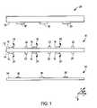
- FIG. 1is a block diagram of an interposer, an electrical contactor and a wafer comprising circuits to be tested;
- FIG. 2is a block diagram of a contactor assembly in accordance with one embodiment of the invention.
- FIG. 4is a perspective view of a vacuum plate connected to a ring, in accordance with one embodiment of the invention.
- FIG. 5is a top plan view of the vacuum plate and ring of FIG. 4 ;
- FIG. 6is a section on 6 — 6 in FIG. 5 ;
- FIG. 7is a block diagram illustrating how a ring and interposer seated therein may be aligned with a contactor, in accordance with one embodiment of the invention.
- FIG. 8is a perspective view of an alignment machine in accordance with one embodiment of the invention.
- FIG. 9is an end view of the alignment machine shown in FIG. 8 of the drawings with a microscope mounted thereon;
- FIG. 10is a perspective view of the alignment machine of FIG. 8 mounted on a probe plate;
- FIG. 11is an end view of FIG. 10 ;
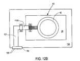
- FIG. 12Ais a block diagram of the probe plate showing a flexible connector in accordance with another embodiment of the invention electrically connecting a contactor assembly to the probe plate;
- FIG. 12Bis a block diagram of a probe plate showing a flexible connector in accordance with one embodiment of the invention electrically connecting a contactor assembly to the probe plate;
- FIGS. 13A and 13Bare block diagrams of an end of the flexible connector of FIG. 12A ;
- FIG. 14shows an arrangement of electrical contact elements on an electrical contactor in accordance with one embodiment of the invention
- FIGS. 15 and 16are block diagrams showing different stages in the formation of an electrical connection between the flexible electrical connector and the electrical contactor of FIG. 12 ;
- FIG. 17is a block diagram of the probe plate of FIG. 12 wherein without the electrical connector and showing fiducial markings on the contactor assembly;
- FIG. 18is a block diagram of a test probe assembly in accordance with one embodiment of the invention.
- FIG. 1 of the accompanying drawingsillustrates an interposer 10 and an electrical contactor 26 which together form a contactor assembly, according to an embodiment of the invention, used to test electrical circuits, for example, on a wafer 32 .
- the interposer 10includes a substrate having a first side 12 and a second side 14 .
- the interposer 10includes a number of electrical terminals 16 on the first side 12 .
- the interposer 10also includes resilient interconnection elements in the form of interconnection spring elements 18 .
- Each interconnection spring element 18extends from an electrical terminal 16 on the side 12 and terminates in a free end.
- the purpose of each interconnection spring elements 16is to make good electrical contact with corresponding electrical terminals on the electrical contactor 26 .
- the resilient interconnection elementsinclude pogo pins and compliant conductive bumps.
- the interposer 10also has an interconnection spring element 20 on each electrical terminal 16 on side 14 .
- the interconnection spring elements 20are similar to the interconnection spring elements 18 except that the interconnection spring elements 20 are for making electrical contact with corresponding electrical terminals on the wafer 32 .
- the interposeralso includes mechanical alignment stops 22 on the sides 12 and 14 to prevent overtravel of the interconnection spring elements 18 and to prevent the interposer from touching certain areas of the wafer 32 .
- the electrical contactor 26includes a contactor substrate which includes a side 28 . Electrical contactor 26 also includes electrical terminals 30 on the side 28 .
- the wafer 32is shown to include a side 34 which has the electrical circuits to be tested.
- the wafer 32has electrical terminals 36 on the side 34 whereby electrical connection to the electrical circuits may be made.
- FIG. 2 of the drawingsshows a contactor assembly 40 in accordance with one embodiment of the invention.
- the assembly 40includes an interposer 10 and a retaining component in the form of a ring 42 .
- the interposer 10is secured or held in a predetermined or aligned position relative to the electrical contactor 26 by a ring 42 . It will be seen that in the predetermined or aligned position, each interconnection spring element 18 has been deformed against a spring force thereof to make electrical contact with a corresponding electrical terminal 30 of electrical contactor 26 .
- the predetermined positionis reached by moving the ring 42 and the interposer 10 seated therein until the alignment stops 22 bear against the side 28 of the electrical contactor 26 .
- the predetermined positionis reached when sufficient pressure is exerted by the interconnection spring elements 18 (or the pogo pins or compliant conductive bumps in other embodiments) to keep the contactor 26 in place.
- the stops 22are thus optional.
- a spacing between the interposer 10 and the electrical contactor 26is such that each of the interconnection spring elements 18 is under compression.
- the ring 42is formed with a recessed surface 44 which defines a seat for the interposer 10 .
- the ring 42has a flat flange-like face 46 which bears against side 28 of electrical contactor 26 .
- the ring 42is secured to the electrical contactor 26 by means of fasteners 43 , for example screws, extending through screw holes 48 (see FIG. 4 ).
- the holes 48are dimensioned to accommodate the fasteners 43 with some degree of play to permit alignment of fiducial markings on the interposer 10 and contactor 26 , respectively.
- FIG. 3 of the drawingsshows a first stage in the formation of the contactor assembly 40 .
- a vacuum plate 50is releasably secured to a side of the ring 42 opposing face 46 to form a sub-assembly 51 .
- the vacuum plate 50can be connected to a pump (not shown) by means of a coupling 54 and a hose 52 connected to the coupling 54 .
- the pumpcreates a vacuum in a region 56 between the vacuum plate 50 the interposer 10 .
- the vacuumretains interposer 10 against the recessed surface 44 .
- the vacuum plate 50is shaped and dimensioned to provide access to the fasteners 43 .
- FIG. 6which shows a sectional view through sub-assembly 51 taken at 6 — 6 in FIG. 5 , the interposer 10 seats snugly in the ring 42 .
- FIG. 7 of the drawingsshows a block diagram of how alignment of the interposer 10 with the electrical contactor 26 is achieved.
- the interposer 10is seated in the ring 42 and moved in an x, y, or ⁇ direction such that a fiducial marking 58 on the side 12 of the interposer 10 is aligned with a fiducial marking 60 on the side 28 of the electrical contactor 26 .
- the ring 42 together with the interposer 10is displaced in a z direction so that the ring 42 makes contact with the electrical contactor 26 .
- a screw 43 located in hole 48is then screw-threaded into a complementary threaded socket 68 formed in electrical contactor 26 .
- the fiducial markings 58 , 60allow for alignment for the electrical terminals 30 on the electrical contactor 26 with the ends of the interconnection spring elements 18 without having to take an image of the interconnection spring elements 18 . Tolerances in the position of each interconnection spring element in the x-y plane or the angle at which it projects from the x-y plane do not effect the alignment process.
- the mechanical stops 22 on the side 18 of the interposer 10may be used to limit movement of the interposer 10 towards the electrical contactor 26 when forming the assembly 40 , such that each of the interconnection spring elements 18 is under the desired compression.
- FIG. 8 of the drawingsshows a perspective view of an alignment machine 70 , in accordance with one embodiment of the invention, which may be used to align the ring 42 and interposer 10 combination with the electrical contactor 26 .
- the alignment machine 70includes a base 72 which is shaped and dimensioned to rest on a probe plate 152 which, in use, houses the electrical contactor 26 .
- the alignment machine 70also includes a raised platform or plate 74 which is secured to the base 72 by means of mounting brackets 76 .
- the platform 74supports a carriage 78 .
- the carriage 78is seen in FIG. 9 of the drawings which shows a side view of the alignment machine 70 .
- the carriage 78is secured to an underside of the platform 74 by means of a mounting arrangement comprising angle brackets 88 and horizontal springs 90 .
- the angle brackets 88are secured to the platform 74 and provide an anchor for one end of the springs 90 , the other end of the springs 90 being secured to a floating plate 80 of carriage 78 as can be seen in FIG. 9 of the drawings.
- the carriage 78further includes ring holders 82 which are secured to the floating plate 80 of vertical members 84 extending between the ring holders mounting plate 82 and the floating plate 80 .
- Roller bearings 94 disposed between the platform 74 and the floating plate 80allow for slidable displacement of the floating plate 80 relative to the platform 74 .
- Vertical springs 95urge the floating plate 80 into contact with roller bearings 94 .
- the spring mounting arrangement of the floating plate 80 to the platform 74allows for movement of the floating plate 80 in an x-y plane.
- Such movement in the x y planeis controlled by means of an adjustment mechanism which, in one embodiment, includes micrometers 96 , 98 , and 100 , each of which can be operated to urge a tip thereof to bear against an edge of the floating plate 80 thereby to cause the displacement of floating plate 80 .
- a tip 98.
- the micrometer 98may be displaced in a y direction to bear against an edge of the floating plate 80 thereby to cause the floating plate 80 to be displaced in the y direction. Because the ring holders 82 are rigidly connected to the floating plate 80 , displacement of the floating plate 80 also causes corresponding displacement of the ring holders 82 .
- the interposer 10which is seated in the ring 42 by means of a suction force created with the aid of the vacuum plate 50 and a pump (not shown) is connected mechanically to the ring holders 82 of the carriage 78 . Thereafter, the alignment machine 70 is positioned on a probe plate 152 as is shown in FIG. 10 . In this position, the ring 42 and the interposer 10 which is seated in the ring 42 is positioned directly over the electrical connector 26 which is seated in the probe plate 152 .
- a magnification systemcomprising a microscope 102 which includes a scope section 104 and a base 106 is secured on the platform 74 as can be seen in FIG. 9 of the drawings.
- the microscope 102magnifies the fiducial markings 58 , 60 on the interposer 10 and the electrical connector 26 , respectively.
- the micrometers 96 , 98 and 100may then be operated to move the carriage 78 , which carries the ring 42 and the interposer 10 with it, so that the interposer 10 may be positioned over the electrical connector 26 in a predetermined or aligned position in which the fiducial markings, 58 , 60 on the interposer 10 and the electrical contactor 26 , respectively, are in alignment.
- the alignment machine 70further includes micrometer heads 108 which may be operated to move the carriage 78 in a z direction which causes the interposer and ring combination to be displaced in the z direction towards the electrical contactor 26 .
- displacement in the z directionis continued until alignment the stops 22 contact the side 28 of electrical contactor 26 , or the desired z position is reached.
- the screws 43are screwed into the sockets 68 in the electrical contactor 26 , thereby to secure the ring 42 and the interposer 10 seated therein to the electrical contactor 26 .
- the probe plate 152includes an external interface component 164 comprising a plurality of electrical connectors in the form of electrical pins 166 as can be seen in FIG. 12 .
- a flexible connector 110electrically connects the contactor assembly 40 to the interface component 164 which in turn is electrically connected to a burn-in chamber of a testing machine (not shown) via the pins 166 .
- the flexible connector 110includes a flexible substrate 112 having sides 112 . 1 and 112 . 2 as can be seen in FIG. 13A . Further, the flexible substrate 112 has a first end 115 and a second end 116 . Flexible line conductors 114 . 1 and 114 . 2 are formed on the sides 112 . 1 and 112 . 2 respectively, as can be seen in FIGS. 13A and 13B of the drawings. Each flexible line conductor 114 . 1 has a first end which is electrically connected to the interface component 164 and a second end remote from the first end. Each flexible line conductor 114 . 1 includes a terminal at its second end comprising two conductive bumps 118 . 1 as can be seen in FIG. 13B of the drawings.
- Each flexible line conductor 114 . 2likewise, has a first end which is electrically connected to the interface component 164 and a second end remote from the first end which is connected by a via 113 extending though the substrate 112 to a terminal comprising two conductive bumps 118 . 2 on the side 112 . 1 . It will be appreciated that by having flexible line conductors on each side 112 . 1 and 112 . 2 of the substrate 112 it is possible for the substrate 112 to carry more line conductors 114 . 1 and 114 . 2 .
- the flexible connector 110is sufficiently flexible so that it can fold onto itself without damage to the flexible substrate 112 , and is typically made of a material such as polyimide.
- the flexible substrate 112may have a thickness of 25.4 microns or 49 microns, although a thickness of up to 125 microns is still flexible in a sense that folding onto itself will still be possible without damage to the flexible substrate 112 .
- the bumps 118 . 1 , 118 . 2are formed of gold and have a width of about 100 micrometers and a height of about 60 micrometers. Gold is preferred as a material for the bumps 118 since it does not oxidize and is able to tolerate temperatures of between 150° C. to 350° C. Further, gold maintains its elasticity within a temperature range of between 180° C. to 240° C.
- the flexible connector 110includes a layer 119 which covers the line conductors 114 . 1 and 114 . 2 .
- the layer 119is made of a non-conductive flexible material as can be seen in FIG. 15 .
- the flexible connector 110is electrically connected to the rigidly, substantially unbendable electrical contactor 26 of the contactor assembly 40 .
- the electrical contactor 26has a plurality of electrical contact elements 120 that are compatible for electrical connection to the conductive bumps 118 . 1 and 118 . 2 of the flexible connector 110 .
- FIG. 15shows a layout of the electrical contact elements 120 on the electrical contactor 26 . Referring to FIG. 15 , it will be seen that the electrical contact elements 120 are generally rectangular and are arranged in two rows 125 . Each of the elements 120 has a flat contact surface 120 . 1 . The contact surfaces 120 . 1 of all the electrical contactor elements 120 are in the same plane.
- each electrical contact element 120has lateral dimensions of 125 and 500 microns and a height of 30 microns. In this embodiment, the electrical contact elements 120 are spaced on a pitch of 100 microns.
- the electrical contactor elements 120are typically formed of gold which provides a fairly robust connection with the conductor bumps 118 . 1 and 118 . 2 .
- the electrical connection between the flexible connector 110 and the electrical contactor 26has a low profile and in one embodiment is only about 6 millimeters high.
- FIG. 15 of the drawingsshows a block diagram of a stage in the formation of the electrical connection between the flexible connector 110 and the electrical contact elements 120 .
- the second end 116 of the flexible electrical connector 110is clamped onto the electrical contactor 26 using a clamp.
- the clampcomprises a first clamping member in the form of an elongate bar 122 of a work hardened metal and a second clamping member which is defined by the electrical contactor 26 .
- a coefficient of thermal expansion of the metal bar 122is matched to a coefficient of thermal expansion of the electrical contactor 26 .
- the coefficient of thermal expansion of the metal bar 122is within 0.5 ppm/° C. of the coefficient of thermal expansion of the electrical contactor 26 .
- the elongate metal bar 122 , the flexible connector 110 , and the electrical contactor 26have axially extending holes to receive a fastening bolt 124 therein.
- a nut 126mates with threads on the bolt 124 and urges the conductive bumps 118 . 1 and 118 . 2 into contact with the electrical contactor elements 120 to a position shown in FIG. 16 of the drawings.
- the clamping force exerted by the fastening bolt 124causes the conductive bumps 118 . 1 and 118 . 2 to bear against the electrical contactor elements 120 which results in an elastic and plastic deformation of the conductive bumps 118 . 1 and 118 . 2 . This ensures good electrical contact between the conductive bumps 118 . 1 and 118 . 2 and the electrical contactor elements 120 .
- the fastening bolt 124may have different thermal coefficients, and due to the high temperatures achieved during the burn-in testing, the fastening bolt 124 may lengthen during the burn-in testing. This results in a gap between a head 124 . 1 , of the fastening bolt 124 , and the metal bar 122 .
- an expander member 128 of resilient materialmay be interposed or sandwiched between the elongate metal bar 122 and the flexible connector 110 as can be seen in FIG. 16 .
- the expander member 128which is compressed under the clamping force generated by tightening of the fastening bolt 124 and relaxes or expands if lengthening of the fastening bolt 124 occurs.
- the expander member 128takes up any gap between the head 124 . 1 and the metal bar 122 , thereby to maintain the clamping force of the fastening bolt 124 .
- the expander memberis of a material that is able to withstand the elevated temperatures within a burn-in chamber. Further, since a height of the conductive bumps 118 . 1 and 118 . 2 may vary, the expander member 128 deforms the flexible substrate 112 , differentially to compensate for variations in the height of the conductive bumps 118 . 1 and 118 . 2 .
- FIG. 12Ashows another embodiment 110 A of a flexible connector.
- the flexible connector 110 Ais similar to the flexible connector 110 , except that each end thereof has conductive bumps similar to the bumps 118 . 1 and 118 . 2 .
- One end of the flexible connection 110 Ais clamped to the electrical contactor 26 as described above and an opposite end of the flexible connector 110 A is clamped, in a similar fashion, to a connector 121 which carries electrical signals to and from the external interface 164 .
- the contactor 26includes fiducial markings 130 (as can be seen in FIG. 17 ) to facilitate alignment of the conductive bumps 118 with the electrical contactor elements 120 prior to clamping.
- the fiducial markings 130are visible through the flexible connector 110 .
- the flexible connector 110has complementary fiducial markings 132 (as can be seen in FIG. 13B ) which can then be aligned with the fiducial markings 130 on the contactor 26 to ensure alignment of the conductive bumps 118 with the contactor elements 120 .
- FIG. 18 of the drawingsillustrates the components of test probe assembly 160 in accordance with one embodiment of the invention.
- the test probe assembly 150includes a probe plate 152 and a chuck plate 154 which together define a space therebetween for receiving a contactor assembly such as the contactor assembly 40 shown in FIG. 2 of the drawings.
- the chuck plate 154has a pedestal 156 which provides support for the wafer 32 .
- the probe plate 152includes a piston 158 which is displaceable in a cylinder 160 by a hydraulic fluid which, in use, is introduced into the chamber 160 through a hose 162 which is releasably connectable to the cylinder 160 .
- the piston 158is connected to an electrical contactor 26 of the contactor assembly 40 .
- airis introduced intro the chamber 160 through hose 162 to urge the piston 158 to move in a z direction, thereby to displace the contactor assembly 40 towards the chuck plate 154 until the mechanical alignment stops 22 on the side 14 of the interposer 10 make contact with the side 34 of the wafer 32 .
- a resiliently deformable member in form of an O-ring 163 positioned between the ring 42 and the chuck plate 154serves to limit or control how much displacement of the contactor assembly 40 is produced by movement of the piston 158 .
- movement of the piston 158does not require precise control.
- the O-ring 163provides a seal between the ring 42 and the chuck plate 154 .
- the O-ring 163allows for variations in which the faces 46 of the ring 42 may not be on the same z-plane by cushioning the ring 42 as it is displaced towards the chuck plate 154 .
- the O-ring 163may be replaced by springs which provide a reaction against movement of the piston 158 .
- the probe assembly 152also includes a securing mechanism to releasably secure or fasten the chuck plate 154 to the probe plate 152 .
- the securing mechanismhas not been shown in FIG. 12 , but includes any suitably clamping arrangement such as the kinematic couplings of U.S. Pat. No. 6,340,895 which is hereby incorporated by reference.
- the test probe assembly 150is then inserted into a test burn-in chamber wherein the electrical connection pins 166 are received in complementary electrical sockets.
Landscapes
- Engineering & Computer Science (AREA)
- Physics & Mathematics (AREA)
- General Physics & Mathematics (AREA)
- Computer Hardware Design (AREA)
- Microelectronics & Electronic Packaging (AREA)
- General Engineering & Computer Science (AREA)
- Power Engineering (AREA)
- Environmental & Geological Engineering (AREA)
- Testing Or Measuring Of Semiconductors Or The Like (AREA)
- Measuring Leads Or Probes (AREA)
Abstract
Description
Claims (4)
Priority Applications (3)
| Application Number | Priority Date | Filing Date | Title |
|---|---|---|---|
| US10/912,785US7046022B2 (en) | 2002-07-16 | 2004-08-06 | Assembly for electrically connecting a test component to a testing machine for testing electrical circuits on the test component |
| US11/433,845US7385407B2 (en) | 2002-07-16 | 2006-05-12 | Assembly for electrically connecting a test component to a testing machine for testing electrical circuits on the test component |
| US12/045,480US7511521B2 (en) | 2002-07-16 | 2008-03-10 | Assembly for electrically connecting a test component to a testing machine for testing electrical circuits on the test component |
Applications Claiming Priority (2)
| Application Number | Priority Date | Filing Date | Title |
|---|---|---|---|
| US10/197,104US6867608B2 (en) | 2002-07-16 | 2002-07-16 | Assembly for electrically connecting a test component to a testing machine for testing electrical circuits on the test component |
| US10/912,785US7046022B2 (en) | 2002-07-16 | 2004-08-06 | Assembly for electrically connecting a test component to a testing machine for testing electrical circuits on the test component |
Related Parent Applications (1)
| Application Number | Title | Priority Date | Filing Date |
|---|---|---|---|
| US10/197,104DivisionUS6867608B2 (en) | 2002-07-16 | 2002-07-16 | Assembly for electrically connecting a test component to a testing machine for testing electrical circuits on the test component |
Related Child Applications (1)
| Application Number | Title | Priority Date | Filing Date |
|---|---|---|---|
| US11/433,845DivisionUS7385407B2 (en) | 2002-07-16 | 2006-05-12 | Assembly for electrically connecting a test component to a testing machine for testing electrical circuits on the test component |
Publications (2)
| Publication Number | Publication Date |
|---|---|
| US20050007132A1 US20050007132A1 (en) | 2005-01-13 |
| US7046022B2true US7046022B2 (en) | 2006-05-16 |
Family
ID=30442900
Family Applications (4)
| Application Number | Title | Priority Date | Filing Date |
|---|---|---|---|
| US10/197,104Expired - LifetimeUS6867608B2 (en) | 2002-07-16 | 2002-07-16 | Assembly for electrically connecting a test component to a testing machine for testing electrical circuits on the test component |
| US10/912,785Expired - LifetimeUS7046022B2 (en) | 2002-07-16 | 2004-08-06 | Assembly for electrically connecting a test component to a testing machine for testing electrical circuits on the test component |
| US11/433,845Expired - LifetimeUS7385407B2 (en) | 2002-07-16 | 2006-05-12 | Assembly for electrically connecting a test component to a testing machine for testing electrical circuits on the test component |
| US12/045,480Expired - LifetimeUS7511521B2 (en) | 2002-07-16 | 2008-03-10 | Assembly for electrically connecting a test component to a testing machine for testing electrical circuits on the test component |
Family Applications Before (1)
| Application Number | Title | Priority Date | Filing Date |
|---|---|---|---|
| US10/197,104Expired - LifetimeUS6867608B2 (en) | 2002-07-16 | 2002-07-16 | Assembly for electrically connecting a test component to a testing machine for testing electrical circuits on the test component |
Family Applications After (2)
| Application Number | Title | Priority Date | Filing Date |
|---|---|---|---|
| US11/433,845Expired - LifetimeUS7385407B2 (en) | 2002-07-16 | 2006-05-12 | Assembly for electrically connecting a test component to a testing machine for testing electrical circuits on the test component |
| US12/045,480Expired - LifetimeUS7511521B2 (en) | 2002-07-16 | 2008-03-10 | Assembly for electrically connecting a test component to a testing machine for testing electrical circuits on the test component |
Country Status (1)
| Country | Link |
|---|---|
| US (4) | US6867608B2 (en) |
Cited By (4)
| Publication number | Priority date | Publication date | Assignee | Title |
|---|---|---|---|---|
| US20070063721A1 (en)* | 2005-09-19 | 2007-03-22 | Formfactor, Inc. | Apparatus And Method Of Testing Singulated Dies |
| US20100134101A1 (en)* | 2008-12-03 | 2010-06-03 | Stmicroelectronics S.R.L. | Broad-range magnetic sensor and manufacturing process thereof |
| US8501502B2 (en)* | 2011-12-28 | 2013-08-06 | Princo Middle East Fze | Package method for electronic components by thin substrate |
| US8658437B2 (en)* | 2011-12-28 | 2014-02-25 | Princo Middle East Fze | Package method for electronic components by thin substrate |
Families Citing this family (24)
| Publication number | Priority date | Publication date | Assignee | Title |
|---|---|---|---|---|
| US20050025449A1 (en)* | 2002-11-08 | 2005-02-03 | Dirkson John C. | Methods and structures for testing optical subassemblies at higher and lower temperatures |
| US6975124B2 (en)* | 2003-09-22 | 2005-12-13 | International Business Machines Corp. | Multipoint nanoprobe |
| US9476911B2 (en) | 2004-05-21 | 2016-10-25 | Microprobe, Inc. | Probes with high current carrying capability and laser machining methods |
| KR20070034595A (en)* | 2004-07-21 | 2007-03-28 | 어포어 오와이 | Pressure test device and pressure test method |
| US7762822B2 (en) | 2005-04-27 | 2010-07-27 | Aehr Test Systems | Apparatus for testing electronic devices |
| US7583100B2 (en)* | 2006-11-30 | 2009-09-01 | Sts Instruments, Inc. | Test head for testing electrical components |
| US7919839B2 (en)* | 2007-07-24 | 2011-04-05 | Northrop Grumman Systems Corporation | Support structures for on-wafer testing of wafer-level packages and multiple wafer stacked structures |
| US7800382B2 (en) | 2007-12-19 | 2010-09-21 | AEHR Test Ststems | System for testing an integrated circuit of a device and its method of use |
| US7936177B2 (en)* | 2008-03-07 | 2011-05-03 | Formfactor, Inc. | Providing an electrically conductive wall structure adjacent a contact structure of an electronic device |
| US8030957B2 (en) | 2009-03-25 | 2011-10-04 | Aehr Test Systems | System for testing an integrated circuit of a device and its method of use |
| US8154119B2 (en) | 2010-03-31 | 2012-04-10 | Toyota Motor Engineering & Manufacturing North America, Inc. | Compliant spring interposer for wafer level three dimensional (3D) integration and method of manufacturing |
| US8829937B2 (en)* | 2011-01-27 | 2014-09-09 | Formfactor, Inc. | Fine pitch guided vertical probe array having enclosed probe flexures |
| MY163629A (en)* | 2011-05-02 | 2017-10-13 | Johnstech Int Corp | Compliant contact plate for use in testing integrated circuits |
| US8803001B2 (en) | 2011-06-21 | 2014-08-12 | Toyota Motor Engineering & Manufacturing North America, Inc. | Bonding area design for transient liquid phase bonding process |
| US10058951B2 (en) | 2012-04-17 | 2018-08-28 | Toyota Motor Engineering & Manufacturing North America, Inc. | Alloy formation control of transient liquid phase bonding |
| US9044822B2 (en) | 2012-04-17 | 2015-06-02 | Toyota Motor Engineering & Manufacturing North America, Inc. | Transient liquid phase bonding process for double sided power modules |
| CN105531593B (en)* | 2013-05-06 | 2019-05-03 | 佛姆法克特股份有限公司 | For testing the probe card assembly of electronic device |
| CN104198866A (en)* | 2014-09-19 | 2014-12-10 | 湖北泰晶电子科技股份有限公司 | Test device for surface mount device tuning fork crystals |
| US10379156B2 (en)* | 2015-05-29 | 2019-08-13 | Taiwan Semiconductor Manufacturing Company, Ltd. | Bump ball testing system and method |
| TWI836645B (en) | 2016-01-08 | 2024-03-21 | 美商艾爾測試系統 | Tester apparatus and method of testing microelectronic device |
| US11079406B2 (en)* | 2016-08-31 | 2021-08-03 | International Business Machines Corporation | Semiconductor micro probe array having compliance |
| KR20250122540A (en) | 2017-03-03 | 2025-08-13 | 에어 테스트 시스템즈 | Cartridge, test piece and method of testing one or more electronic devices |
| EP4226165A4 (en) | 2020-10-07 | 2024-10-30 | AEHR Test Systems | Electronics tester |
| WO2023049281A2 (en)* | 2021-09-22 | 2023-03-30 | Samtec, Inc. | Rf connector mounting |
Citations (8)
| Publication number | Priority date | Publication date | Assignee | Title |
|---|---|---|---|---|
| US4783719A (en)* | 1987-01-20 | 1988-11-08 | Hughes Aircraft Company | Test connector for electrical devices |
| US5313157A (en) | 1990-10-31 | 1994-05-17 | Hughes Aircraft Company | Probe for jesting an electrical circuit chip |
| EP0639777A1 (en) | 1993-08-21 | 1995-02-22 | Hewlett-Packard Company | Inspecting electrical components using a probe |
| US6005401A (en) | 1993-12-16 | 1999-12-21 | Matsushita Electric Industrial Co., Ltd. | Semiconductor wafer package, method and apparatus for connecting testing IC terminals of semiconductor wafer and probe terminals, testing method of a semiconductor integrated circuit, probe card and its manufacturing method |
| US6137297A (en) | 1999-01-06 | 2000-10-24 | Vertest Systemsn Corp. | Electronic test probe interface assembly and method of manufacture |
| US6292007B1 (en) | 1997-05-19 | 2001-09-18 | Si Diamond Technology Inc. | Probe head assembly |
| US20020075025A1 (en) | 1999-06-30 | 2002-06-20 | Masahiro Tanaka | Semiconductor testing tool |
| US6897672B2 (en)* | 2001-06-25 | 2005-05-24 | Micron Technology, Inc. | Apparatus to prevent damage to probe card |
Family Cites Families (7)
| Publication number | Priority date | Publication date | Assignee | Title |
|---|---|---|---|---|
| US3654585A (en)* | 1970-03-11 | 1972-04-04 | Brooks Research And Mfg Inc | Coordinate conversion for the testing of printed circuit boards |
| JPH07115113A (en)* | 1993-08-25 | 1995-05-02 | Nec Corp | Semiconductor wafer testing device and testing method |
| US5974662A (en)* | 1993-11-16 | 1999-11-02 | Formfactor, Inc. | Method of planarizing tips of probe elements of a probe card assembly |
| US6577148B1 (en)* | 1994-08-31 | 2003-06-10 | Motorola, Inc. | Apparatus, method, and wafer used for testing integrated circuits formed on a product wafer |
| US5600257A (en)* | 1995-08-09 | 1997-02-04 | International Business Machines Corporation | Semiconductor wafer test and burn-in |
| US6483328B1 (en) | 1995-11-09 | 2002-11-19 | Formfactor, Inc. | Probe card for probing wafers with raised contact elements |
| JP4047116B2 (en)* | 2002-09-19 | 2008-02-13 | キヤノン株式会社 | Image forming system |
- 2002
- 2002-07-16USUS10/197,104patent/US6867608B2/ennot_activeExpired - Lifetime
- 2004
- 2004-08-06USUS10/912,785patent/US7046022B2/ennot_activeExpired - Lifetime
- 2006
- 2006-05-12USUS11/433,845patent/US7385407B2/ennot_activeExpired - Lifetime
- 2008
- 2008-03-10USUS12/045,480patent/US7511521B2/ennot_activeExpired - Lifetime
Patent Citations (9)
| Publication number | Priority date | Publication date | Assignee | Title |
|---|---|---|---|---|
| US4783719A (en)* | 1987-01-20 | 1988-11-08 | Hughes Aircraft Company | Test connector for electrical devices |
| US5313157A (en) | 1990-10-31 | 1994-05-17 | Hughes Aircraft Company | Probe for jesting an electrical circuit chip |
| EP0639777A1 (en) | 1993-08-21 | 1995-02-22 | Hewlett-Packard Company | Inspecting electrical components using a probe |
| US5491427A (en)* | 1993-08-21 | 1996-02-13 | Hewlett-Packard Company | Probe and electrical part/circuit inspecting apparatus as well as electrical part/circuit inspecting method |
| US6005401A (en) | 1993-12-16 | 1999-12-21 | Matsushita Electric Industrial Co., Ltd. | Semiconductor wafer package, method and apparatus for connecting testing IC terminals of semiconductor wafer and probe terminals, testing method of a semiconductor integrated circuit, probe card and its manufacturing method |
| US6292007B1 (en) | 1997-05-19 | 2001-09-18 | Si Diamond Technology Inc. | Probe head assembly |
| US6137297A (en) | 1999-01-06 | 2000-10-24 | Vertest Systemsn Corp. | Electronic test probe interface assembly and method of manufacture |
| US20020075025A1 (en) | 1999-06-30 | 2002-06-20 | Masahiro Tanaka | Semiconductor testing tool |
| US6897672B2 (en)* | 2001-06-25 | 2005-05-24 | Micron Technology, Inc. | Apparatus to prevent damage to probe card |
Cited By (7)
| Publication number | Priority date | Publication date | Assignee | Title |
|---|---|---|---|---|
| US20070063721A1 (en)* | 2005-09-19 | 2007-03-22 | Formfactor, Inc. | Apparatus And Method Of Testing Singulated Dies |
| US7733106B2 (en)* | 2005-09-19 | 2010-06-08 | Formfactor, Inc. | Apparatus and method of testing singulated dies |
| US20100244873A1 (en)* | 2005-09-19 | 2010-09-30 | Formfactor, Inc. | Apparatus and method of testing singulated dies |
| US8513969B2 (en) | 2005-09-19 | 2013-08-20 | Formfactor, Inc. | Apparatus and method of testing singulated dies |
| US20100134101A1 (en)* | 2008-12-03 | 2010-06-03 | Stmicroelectronics S.R.L. | Broad-range magnetic sensor and manufacturing process thereof |
| US8501502B2 (en)* | 2011-12-28 | 2013-08-06 | Princo Middle East Fze | Package method for electronic components by thin substrate |
| US8658437B2 (en)* | 2011-12-28 | 2014-02-25 | Princo Middle East Fze | Package method for electronic components by thin substrate |
Also Published As
| Publication number | Publication date |
|---|---|
| US20080150560A1 (en) | 2008-06-26 |
| US6867608B2 (en) | 2005-03-15 |
| US20050007132A1 (en) | 2005-01-13 |
| US20040012403A1 (en) | 2004-01-22 |
| US7511521B2 (en) | 2009-03-31 |
| US20060267624A1 (en) | 2006-11-30 |
| US7385407B2 (en) | 2008-06-10 |
Similar Documents
| Publication | Publication Date | Title |
|---|---|---|
| US7511521B2 (en) | Assembly for electrically connecting a test component to a testing machine for testing electrical circuits on the test component | |
| US7301358B2 (en) | Contactor assembly for testing electrical circuits | |
| US7872482B2 (en) | High density interconnect system having rapid fabrication cycle | |
| US7195503B2 (en) | Electrical contactor, especially wafer level contactor, using fluid pressure | |
| WO2004008163A2 (en) | Assembly for connecting a test device to an object to be tested | |
| US6756797B2 (en) | Planarizing interposer for thermal compensation of a probe card | |
| US7808259B2 (en) | Component assembly and alignment | |
| JP4704426B2 (en) | Electrical connection device, method of manufacturing the same, and electrical connection device | |
| TWI550276B (en) | Probe card assembly, stiffener for use with a probe card assembly, and test apparatus | |
| US7382143B2 (en) | Wafer probe interconnect system | |
| JPWO2008146705A1 (en) | Probe card fixing device | |
| KR100707044B1 (en) | Structure of integrated circuit wafer probe card assembly and its manufacturing method | |
| US20080100323A1 (en) | Low cost, high pin count, wafer sort automated test equipment (ate) device under test (dut) interface for testing electronic devices in high parallelism | |
| JP2000055983A (en) | Carrier board for testing IC devices | |
| KR101922848B1 (en) | Probe card with elastic body | |
| HK1060399B (en) | Planarizing interposer |
Legal Events
| Date | Code | Title | Description |
|---|---|---|---|
| STCF | Information on status: patent grant | Free format text:PATENTED CASE | |
| FPAY | Fee payment | Year of fee payment:4 | |
| SULP | Surcharge for late payment | ||
| AS | Assignment | Owner name:SILICON VALLEY BANK, CALIFORNIA Free format text:SECURITY AGREEMENT;ASSIGNOR:AEHR TEST SYSTEMS;REEL/FRAME:031171/0001 Effective date:20130821 | |
| FPAY | Fee payment | Year of fee payment:8 | |
| AS | Assignment | Owner name:AEHR TEST SYSTEMS, CALIFORNIA Free format text:RELEASE BY SECURED PARTY;ASSIGNOR:SILICON VALLEY BANK;REEL/FRAME:035420/0390 Effective date:20150410 | |
| AS | Assignment | Owner name:QUINTESSENCE FUND L.P., NEW YORK Free format text:SECURITY INTEREST;ASSIGNOR:AEHR TEST SYSTEMS;REEL/FRAME:035424/0783 Effective date:20150410 Owner name:QVT FUND LP, NEW YORK Free format text:SECURITY INTEREST;ASSIGNOR:AEHR TEST SYSTEMS;REEL/FRAME:035424/0783 Effective date:20150410 | |
| FEPP | Fee payment procedure | Free format text:MAINTENANCE FEE REMINDER MAILED (ORIGINAL EVENT CODE: REM.) | |
| FEPP | Fee payment procedure | Free format text:11.5 YR SURCHARGE- LATE PMT W/IN 6 MO, SMALL ENTITY (ORIGINAL EVENT CODE: M2556) | |
| MAFP | Maintenance fee payment | Free format text:PAYMENT OF MAINTENANCE FEE, 12TH YR, SMALL ENTITY (ORIGINAL EVENT CODE: M2553) Year of fee payment:12 | |
| AS | Assignment | Owner name:AEHR TEST SYSTEMS, CALIFORNIA Free format text:RELEASE BY SECURED PARTY;ASSIGNORS:QVT FUND LP;QUINTESSENCE FUND L.P.;REEL/FRAME:050928/0695 Effective date:20191031 |