US7045791B2 - Column simultaneously focusing a partilce beam and an optical beam - Google Patents
Column simultaneously focusing a partilce beam and an optical beamDownload PDFInfo
- Publication number
- US7045791B2 US7045791B2US10/239,293US23929303AUS7045791B2US 7045791 B2US7045791 B2US 7045791B2US 23929303 AUS23929303 AUS 23929303AUS 7045791 B2US7045791 B2US 7045791B2
- Authority
- US
- United States
- Prior art keywords
- optical
- column
- focusing device
- particle
- outlet aperture
- Prior art date
- Legal status (The legal status is an assumption and is not a legal conclusion. Google has not performed a legal analysis and makes no representation as to the accuracy of the status listed.)
- Expired - Fee Related, expires
Links
Images


Classifications
- H—ELECTRICITY
- H01—ELECTRIC ELEMENTS
- H01J—ELECTRIC DISCHARGE TUBES OR DISCHARGE LAMPS
- H01J37/00—Discharge tubes with provision for introducing objects or material to be exposed to the discharge, e.g. for the purpose of examination or processing thereof
- H01J37/02—Details
- H01J37/22—Optical, image processing or photographic arrangements associated with the tube
- H01J37/226—Optical arrangements for illuminating the object; optical arrangements for collecting light from the object
- H01J37/228—Optical arrangements for illuminating the object; optical arrangements for collecting light from the object whereby illumination or light collection take place in the same area of the discharge
- H—ELECTRICITY
- H01—ELECTRIC ELEMENTS
- H01J—ELECTRIC DISCHARGE TUBES OR DISCHARGE LAMPS
- H01J37/00—Discharge tubes with provision for introducing objects or material to be exposed to the discharge, e.g. for the purpose of examination or processing thereof
- H01J37/02—Details
- H01J37/04—Arrangements of electrodes and associated parts for generating or controlling the discharge, e.g. electron-optical arrangement or ion-optical arrangement
- H01J37/10—Lenses
- H01J37/12—Lenses electrostatic
- H—ELECTRICITY
- H01—ELECTRIC ELEMENTS
- H01J—ELECTRIC DISCHARGE TUBES OR DISCHARGE LAMPS
- H01J37/00—Discharge tubes with provision for introducing objects or material to be exposed to the discharge, e.g. for the purpose of examination or processing thereof
- H01J37/30—Electron-beam or ion-beam tubes for localised treatment of objects
- H01J37/304—Controlling tubes by information coming from the objects or from the beam, e.g. correction signals
- H—ELECTRICITY
- H01—ELECTRIC ELEMENTS
- H01J—ELECTRIC DISCHARGE TUBES OR DISCHARGE LAMPS
- H01J37/00—Discharge tubes with provision for introducing objects or material to be exposed to the discharge, e.g. for the purpose of examination or processing thereof
- H01J37/30—Electron-beam or ion-beam tubes for localised treatment of objects
- H01J37/305—Electron-beam or ion-beam tubes for localised treatment of objects for casting, melting, evaporating, or etching
- H01J37/3053—Electron-beam or ion-beam tubes for localised treatment of objects for casting, melting, evaporating, or etching for evaporating or etching
- H01J37/3056—Electron-beam or ion-beam tubes for localised treatment of objects for casting, melting, evaporating, or etching for evaporating or etching for microworking, e. g. etching of gratings or trimming of electrical components
- G—PHYSICS
- G02—OPTICS
- G02B—OPTICAL ELEMENTS, SYSTEMS OR APPARATUS
- G02B17/00—Systems with reflecting surfaces, with or without refracting elements
- G02B17/08—Catadioptric systems
- G02B17/082—Catadioptric systems using three curved mirrors
- H—ELECTRICITY
- H01—ELECTRIC ELEMENTS
- H01J—ELECTRIC DISCHARGE TUBES OR DISCHARGE LAMPS
- H01J2237/00—Discharge tubes exposing object to beam, e.g. for analysis treatment, etching, imaging
- H01J2237/10—Lenses
- H01J2237/12—Lenses electrostatic
- H01J2237/121—Lenses electrostatic characterised by shape
- H—ELECTRICITY
- H01—ELECTRIC ELEMENTS
- H01J—ELECTRIC DISCHARGE TUBES OR DISCHARGE LAMPS
- H01J2237/00—Discharge tubes exposing object to beam, e.g. for analysis treatment, etching, imaging
- H01J2237/248—Components associated with the control of the tube
- H01J2237/2482—Optical means
- H—ELECTRICITY
- H01—ELECTRIC ELEMENTS
- H01J—ELECTRIC DISCHARGE TUBES OR DISCHARGE LAMPS
- H01J2237/00—Discharge tubes exposing object to beam, e.g. for analysis treatment, etching, imaging
- H01J2237/30—Electron or ion beam tubes for processing objects
- H01J2237/317—Processing objects on a microscale
- H01J2237/31749—Focused ion beam
Definitions
- This inventionrelates that to an optical column for simultaneously focusing an ion beam and a photon beam onto the same region.
- the inventionis particularly useful in the field of analysis and repair and manufacture of integrated circuits.
- Focused ion beamssuch as ion or electron beams are currently widely used for various types of integrated circuit analysis and manufacturing operations, notably characterisation, identification, design and failure analysis, depassivation, vapor phase deposition, micro-machining, etc. These operations are performed using a particle beam production column designed to be focused onto the integrated circuit at the place intended for the desired intervention.
- Such a columntypically comprises a source of ions such as Ga+ produced from liquid metal which, after extraction, form an ion beam, which is then manipulated by a focusing device comprising a certain number of electrodes operating at determined potentials so as to form an electrostatic lens system adapted to focus the ion beam onto the integrated circuit.
- a focusing devicecomprising a certain number of electrodes operating at determined potentials so as to form an electrostatic lens system adapted to focus the ion beam onto the integrated circuit.
- Each electrode of the focusing devicenotably the output electrode, consists of a series of metallic electrodes having an aperture for passage of the particle beam. It should be noted here that the shape of the various electrodes as well as the aperture diameter plays a determining part in aberrations, notably spherical and chromatic aberration, of the particle focusing device.
- Certain ion beam production columnsalso include an optical focusing device, a Cassegrain-Schwartzfeld (C-S) mirror objective lens for example, terminating at an outlet aperture placed close to the surface of a sample subjected to the ion beam.
- C-SCassegrain-Schwartzfeld
- French patent 2,437,695discloses an emission ion lens associated with a C-S type mirror objective lens.
- the ionic lens partthe elements of which consist of two perforated electrodes and of the sample itself, is located between the object and the mirror objective lens.
- the apertures in the ion focusing device electrodesmust simultaneously be sufficiently large to provide a geometrical expanse for the optical beam allowing sufficient sample illumination, and, relatively small so as not to deteriorate ion beam quality through excessive aberrations.
- the final diameter chosen for the outlet apertureis consequently a trade-off which is not satisfactory either for the optical beam extent or for ion beam focusing.
- a focused particle beam production columncomprising:
- a device for focusing said particlescarrying an output electrode having an outlet aperture for the passage of said particle beam
- an optical focusing devicefor simultaneously focusing a light beam, carrying an outlet opening
- the solution to the technical problem posedconsists, according to this invention, in that the outlet opening is transparent to said light beam, said output electrode being formed by a metal insert held in said opening and carrying a central aperture forming said outlet aperture.
- the column of the inventionintroduces independence between outlet aperture diameter of the particle focusing device and outlet aperture diameter of the optical focusing device. It is thus possible to adjust central aperture diameter of the metal insert to an optimum value for reducing output electrode aberrations, without this in any way prejudicing optical beam numerical aperture, the latter being determined by the diameter of the aperture transparent to the optical beam.
- the particle focusing devicewith said particle focusing device including an intermediate electrode, for the metal insert to project from the opening towards the intermediate electrode.
- said particle focusing deviceincluding an intermediate electrode, for the metal insert to project from the opening towards the intermediate electrode.
- the particle production column of the inventionis suited to a great number of applications including:
- FIG. 1is a partial side view in section of a particle beam production column according to one first embodiment of the invention.
- FIG. 2is a partial side view in section of a particle beam production column according to a second embodiment of the invention.
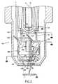
- FIG. 1we have partially shown, in section, a particle beam production column for focusing onto an integrated circuit 1 .
- the particle beam axis which coincides with the column axisis identified by reference letter A.
- the column in FIG. 1applies to all sorts of charged particles, electrons or ions, we shall take below the example of an ion beam.
- FIG. 1Only the downstream part of the column is shown in FIG. 1 , the ion source and the means for extracting and conditioning the ion beam which are known per se, not being shown.
- the part of the column shown in FIG. 1essentially comprises a device 100 for focusing the ion beam onto integrated circuit 1 .
- This device 100carries three electrodes, specifically an input electrode 110 which is grounded, an intermediate electrode 120 brought to a nonzero potential V which may be positive or negative for example of 20 Kev, and an output electrode 130 also grounded. These electrodes 110 , 120 , 130 are contained between lateral walls 140 of the column, the latter being grounded.
- intermediate electrode 120is a complex two-part electrode made up by a first intermediate electrode 121 arranged close to input electrode 110 and by a second intermediate electrode 122 arranged close to output electrode 130 . These electrodes together form an electrostatic lens of the thick, geometrically asymmetric but electrically symmetric type.
- an optical focusing device 200designed to focus an optical beam F simultaneously and coaxially with the particle beam on axis A is located between the two intermediate electrodes 121 , 122 .
- This device 200allows both optical beam F to be focused onto sample 1 thereby forming an enlarged image of the sample as well as collection of light radiation emitted by said sample or by sputtered atoms following ionic bombardment.
- Optical beam Fis obtained from a non-illustrated light source generally arranged laterally with respect to the column with the light being re-directed parallel to axis A and by a mirror at 45° located on said axis and including an aperture for passage of the ion beam.
- optical focusing device 200is a Cassegrain-type mirror objective lens comprising a first convex spherical mirror 210 located in optical beam path F and a second concave spherical mirror 220 focusing onto integrated circuit 1 the beam coming from first mirror 210 .
- the latterincludes an aperture 211 for allowing the ion beam to pass through the second intermediate electrode 122 , the assembly formed by the first mirror 210 and said second intermediate electrode 122 being held at the centre of the column by a metal tripod 212 providing a high degree of transparency to the light beam.
- optical focusing device 200also carries an outlet aperture 230 itself including a window 240 that is transparent to photons of optical beam F, held by its edges to the outer housing of the grounded column.
- Output electrode 130is formed by a metal insert passing through a window 240 , and which is retained by said window 240 and including a central aperture at its middle 131 for the output of electrode 130 .
- transparent window 240is electrically conducting. In particular, it can be glass-plated covered with at least one conducting layer 241 such as indium and/or tin oxide.
- outlet window 240could just as well be made of any bulk material transparent to photons, and electrically conducting.
- metal insert 130projects from the surface of window 240 towards second intermediate electrode 122 , thereby protecting said window in the case of electrical breakdown, the latter occurring between insert 130 and the second electrode 122 .
- optical focusing device 200 of the embodiment of the invention shown in FIG. 2is a Cassegrain-type objective lens with mirrors 210 , 220 brought to a high-voltage comprised, for example, between 10 and 20 keV.
- a first mirror 300is located on ion beam axis A between the first intermediate electrode 121 and the second intermediate electrode 122 and, more precisely, between first intermediate electrode 121 and the Cassegrain-type objective lens with mirrors 210 , 220 .
- This mirror 300carries an aperture 310 for passage of the ion beam. It is inclined substantially at 45° with respect to axis A in order to deflect optical beam F through about 90° laterally towards a second mirror 320 arranged in the space comprised between the lateral walls 140 of the column and part 120 .
- This second mirror 320is itself angled at 45° with respect to axis A. It deflects beam F through 90 degrees in the same direction as axis A, parallel to the latter.
- the diameter of aperture 111 provided at the extremity of input electrode 110designed to allow passage of ion beam A but the function of which is not, contrary to the embodiment of FIG. 1 , to allow passage of the optical beam, can be reduced to values of millimetric scale order.
- deflector plates 10 located upstream of input electrode 110no longer require the anti-reflection treatment needed for good conduction of the optical beam.
- artefacts due to the light beam interacting with the walls of the ionic optical elements which did exist upstream of first mirror 300in particular at deflector plates 10 of the embodiment in FIG. 1 and which notably decrease quality of interpretation of the images obtained, are eliminated.
- aperture 230does not carry a window 240 but rather a set of metallic or, at the least electrically-conducting, tabs or legs.
- tabsThere are for example three such tabs forming a metallic tripod 250 which is retained by the edges of the outer housing of the grounded column, delimiting aperture 230 . They ensure good retention of insert 150 while ensuring aperture 230 is kept transparent for the optical beam.
- the tabs or legs of metal tripod 212 designed to hold the unit formed by mirror 210 and the second intermediate electrode 122are curved so as to increase their spacing from the legs of tripod 250 and output electrode 130 . Thanks to this, risks of spark-over are limited as are distortions of the electrical field due to the tripod.
Landscapes
- Chemical & Material Sciences (AREA)
- Analytical Chemistry (AREA)
- Physics & Mathematics (AREA)
- Engineering & Computer Science (AREA)
- Plasma & Fusion (AREA)
- Analysing Materials By The Use Of Radiation (AREA)
- Electron Tubes For Measurement (AREA)
Abstract
Description
Claims (20)
Priority Applications (2)
| Application Number | Priority Date | Filing Date | Title |
|---|---|---|---|
| US11/295,801US7297948B2 (en) | 2000-03-20 | 2005-12-06 | Column simultaneously focusing a particle beam and an optical beam |
| US11/930,734US7573050B2 (en) | 2000-03-20 | 2007-10-31 | Column simultaneously focusing a particle beam and an optical beam |
Applications Claiming Priority (3)
| Application Number | Priority Date | Filing Date | Title |
|---|---|---|---|
| FR00/03501 | 2000-03-20 | ||
| FR0003501AFR2806527B1 (en) | 2000-03-20 | 2000-03-20 | SIMULTANEOUS FOCUSING COLUMN OF PARTICLE BEAM AND OPTICAL BEAM |
| PCT/FR2001/000812WO2001071766A1 (en) | 2000-03-20 | 2001-03-19 | Column simultaneously focusing a particle beam and an optical beam |
Related Child Applications (1)
| Application Number | Title | Priority Date | Filing Date |
|---|---|---|---|
| US11/295,801ContinuationUS7297948B2 (en) | 2000-03-20 | 2005-12-06 | Column simultaneously focusing a particle beam and an optical beam |
Publications (2)
| Publication Number | Publication Date |
|---|---|
| US20030102436A1 US20030102436A1 (en) | 2003-06-05 |
| US7045791B2true US7045791B2 (en) | 2006-05-16 |
Family
ID=8848259
Family Applications (3)
| Application Number | Title | Priority Date | Filing Date |
|---|---|---|---|
| US10/239,293Expired - Fee RelatedUS7045791B2 (en) | 2000-03-20 | 2001-03-19 | Column simultaneously focusing a partilce beam and an optical beam |
| US11/295,801Expired - LifetimeUS7297948B2 (en) | 2000-03-20 | 2005-12-06 | Column simultaneously focusing a particle beam and an optical beam |
| US11/930,734Expired - LifetimeUS7573050B2 (en) | 2000-03-20 | 2007-10-31 | Column simultaneously focusing a particle beam and an optical beam |
Family Applications After (2)
| Application Number | Title | Priority Date | Filing Date |
|---|---|---|---|
| US11/295,801Expired - LifetimeUS7297948B2 (en) | 2000-03-20 | 2005-12-06 | Column simultaneously focusing a particle beam and an optical beam |
| US11/930,734Expired - LifetimeUS7573050B2 (en) | 2000-03-20 | 2007-10-31 | Column simultaneously focusing a particle beam and an optical beam |
Country Status (6)
| Country | Link |
|---|---|
| US (3) | US7045791B2 (en) |
| EP (1) | EP1292965A1 (en) |
| AU (1) | AU2001246611A1 (en) |
| FR (1) | FR2806527B1 (en) |
| TW (1) | TW591703B (en) |
| WO (1) | WO2001071766A1 (en) |
Cited By (16)
| Publication number | Priority date | Publication date | Assignee | Title |
|---|---|---|---|---|
| US20060076503A1 (en)* | 2004-10-12 | 2006-04-13 | Credence Systems Corporation | Optical coupling apparatus for a dual column charged particle beam tool for imaging and forming silicide in a localized manner |
| US20070115468A1 (en)* | 2005-10-28 | 2007-05-24 | Barnard Bryan R | Spectrometer for surface analysis and method therefor |
| US20080185509A1 (en)* | 2007-02-06 | 2008-08-07 | Fei Company | Particle-optical apparatus for simultaneous observing a sample with particles and photons |
| US20080283777A1 (en)* | 2007-05-16 | 2008-11-20 | International Business Machines Corporation | In-situ high-resolution light-optical channel for optical viewing and surface processing in parallel with charged particle (fib and sem) techniques |
| EP2105943A2 (en) | 2008-03-28 | 2009-09-30 | FEI Company | Environmental cell for a particle-optical apparatus |
| US20100051828A1 (en)* | 2008-09-01 | 2010-03-04 | Carl Zeiss Nts Gmbh | Processing system |
| US20100051802A1 (en)* | 2008-08-29 | 2010-03-04 | Omniprobe, Inc. | Single-channel optical processing system for energetic-beam microscopes |
| US20100163729A1 (en)* | 2008-12-26 | 2010-07-01 | Kabushiki Kaisha Topcon | Electron microscope device |
| US20110115129A1 (en)* | 2008-07-09 | 2011-05-19 | Fei Company | Method and Apparatus for Laser Machining |
| US20110226949A1 (en)* | 2010-03-18 | 2011-09-22 | Carl Zeiss NTSGmbH | Inspection System |
| US20110315877A1 (en)* | 2010-06-24 | 2011-12-29 | Kabushiki Kaisha Topcon | Electron Microscope Device |
| US8440969B2 (en) | 2010-08-02 | 2013-05-14 | Omniprobe, Inc. | Method and apparatus for acquiring simultaneous and overlapping optical and charged particle beam images |
| US8648301B2 (en) | 2011-09-22 | 2014-02-11 | Carl Zeiss Microscopy Ltd. | Particle beam system having a hollow light guide |
| US20160020062A1 (en)* | 2014-07-17 | 2016-01-21 | Fei Company | Charged-Particle Lens that Transmits Emissions from Sample |
| US10546719B2 (en) | 2017-06-02 | 2020-01-28 | Fei Company | Face-on, gas-assisted etching for plan-view lamellae preparation |
| DE102024004479B3 (en) | 2024-04-09 | 2025-10-02 | Carl Zeiss Microscopy Gmbh | Method for operating a particle beam microscope, particle beam microscope and computer program product |
Families Citing this family (14)
| Publication number | Priority date | Publication date | Assignee | Title |
|---|---|---|---|---|
| FR2806527B1 (en) | 2000-03-20 | 2002-10-25 | Schlumberger Technologies Inc | SIMULTANEOUS FOCUSING COLUMN OF PARTICLE BEAM AND OPTICAL BEAM |
| US8202440B1 (en)* | 2002-08-27 | 2012-06-19 | Kla-Tencor Corporation | Methods and apparatus for electron beam assisted etching at low temperatures |
| JP5107506B2 (en)* | 2002-11-12 | 2012-12-26 | エフ・イ−・アイ・カンパニー | Defect analyzer |
| NL1026547C2 (en)* | 2004-07-01 | 2006-01-03 | Fei Co | Device for evacuating a sample. |
| US7245133B2 (en) | 2004-07-13 | 2007-07-17 | Credence Systems Corporation | Integration of photon emission microscope and focused ion beam |
| US7439168B2 (en) | 2004-10-12 | 2008-10-21 | Dcg Systems, Inc | Apparatus and method of forming silicide in a localized manner |
| EP1724809A1 (en)* | 2005-05-18 | 2006-11-22 | FEI Company | Particle-optical apparatus for the irradiation of a sample |
| US7842920B2 (en)* | 2006-12-14 | 2010-11-30 | Dcg Systems, Inc. | Methods and systems of performing device failure analysis, electrical characterization and physical characterization |
| EP1956632A1 (en)* | 2007-02-14 | 2008-08-13 | FEI Company | Particle-optical apparatus for simultaneous observing a sample with particles and photons |
| JP5756585B2 (en)* | 2010-04-07 | 2015-07-29 | エフ・イ−・アイ・カンパニー | Combined laser and charged particle beam system |
| CN102971823B (en)* | 2010-07-08 | 2016-03-30 | Fei公司 | There is the charged particle beam treatment system of visible ray and infrared imaging |
| JP5825964B2 (en)* | 2011-10-05 | 2015-12-02 | 株式会社日立ハイテクノロジーズ | Inspection or observation device and sample inspection or observation method |
| US9991091B1 (en) | 2015-07-02 | 2018-06-05 | Battelle Memorial Institute | Optical column for focused ion beam workstation |
| EP3966844A2 (en)* | 2019-05-09 | 2022-03-16 | Attolight AG | Cathodoluminescence electron microscope |
Citations (64)
| Publication number | Priority date | Publication date | Assignee | Title |
|---|---|---|---|---|
| US3845305A (en) | 1972-05-12 | 1974-10-29 | Max Planck Gesellschaft | Microbeam probe apparatus |
| FR2245937A1 (en)* | 1973-10-01 | 1975-04-25 | Beauvineau Jacky | Study of luminescent materials by electron beam microscope - involves spectroscope with slit adjustable in height and width |
| US3936639A (en) | 1974-05-01 | 1976-02-03 | Raytheon Company | Radiographic imaging system for high energy radiation |
| US3961197A (en) | 1974-08-21 | 1976-06-01 | The United States Of America As Represented By The United States Energy Research And Development Administration | X-ray generator |
| US3970960A (en) | 1974-01-31 | 1976-07-20 | Bell Telephone Laboratories, Incorporated | Broadly tunable continuous-wave laser using color centers |
| US4009391A (en) | 1974-06-25 | 1977-02-22 | Jersey Nuclear-Avco Isotopes, Inc. | Suppression of unwanted lasing in laser isotope separation |
| US4017730A (en) | 1974-05-01 | 1977-04-12 | Raytheon Company | Radiographic imaging system for high energy radiation |
| US4076420A (en) | 1974-02-22 | 1978-02-28 | Max-Planck-Gesellschaft Zur Forderung Der Wissenschaften E.V. | Apparatus for investigating fast chemical reactions by optical detection |
| US4087763A (en) | 1975-11-10 | 1978-05-02 | The United States Of America As Represented By The United States Department Of Energy | Method and apparatus for secondary laser pumping by electron beam excitation |
| US4153675A (en) | 1975-10-20 | 1979-05-08 | Marcos Kleinerman | Immunofluorometric method and apparatus for measuring minute quantities of antigens, antibodies and other substances |
| FR2437695A1 (en) | 1978-09-29 | 1980-04-25 | Max Planck Gesellschaft | ELECTROSTATIC TRANSMISSION LENS |
| US4330295A (en) | 1979-03-05 | 1982-05-18 | Wisconsin Alumni Research Foundation | Microwave discharge degradation of organics for analysis |
| US4345331A (en) | 1980-01-14 | 1982-08-17 | Locke Technology, Inc. | Apparatus for generating an electric field |
| US4418283A (en) | 1978-07-24 | 1983-11-29 | Thomson-Csf | Microlithographic system using a charged particle beam |
| US4440475A (en)* | 1981-01-23 | 1984-04-03 | Compagnie D'applications Mecaniques A L'electronique, Au Cinema Et A L'atomistique (C.A.M.E.C.A.) | Electron probe microanalyzer comprising an observation system having double magnification |
| US4443278A (en) | 1981-05-26 | 1984-04-17 | International Business Machines Corporation | Inspection of multilayer ceramic circuit modules by electrical inspection of green specimens |
| US4551599A (en) | 1982-08-20 | 1985-11-05 | Max-Planck-Gesellschaft Zur Furderung Der Wissenschaften E.V. | Combined electrostatic objective and emission lens |
| US4578279A (en) | 1981-05-26 | 1986-03-25 | International Business Machines Corporation | Inspection of multilayer ceramic circuit modules by electrical inspection of unfired green sheets |
| US4670685A (en) | 1986-04-14 | 1987-06-02 | Hughes Aircraft Company | Liquid metal ion source and alloy for ion emission of multiple ionic species |
| US4673257A (en) | 1985-06-19 | 1987-06-16 | Avco Corporation | Method of and apparatus for correction of laser beam phase front aberrations |
| US4714902A (en) | 1985-06-17 | 1987-12-22 | Avco Everett Research Laboratory, Inc. | Gaseous non linear dispersion laser beam control |
| US4755683A (en) | 1987-10-05 | 1988-07-05 | Oregon Graduate Center | Liquid-metal ion beam source substructure |
| US4764674A (en)* | 1985-06-11 | 1988-08-16 | Hamamatsu Photonics Kabushiki Kaisha | High time resolution electron microscope |
| US4782840A (en) | 1984-03-02 | 1988-11-08 | Neoprobe Corporation | Method for locating, differentiating, and removing neoplasms |
| US4788431A (en) | 1987-04-10 | 1988-11-29 | The Perkin-Elmer Corporation | Specimen distance measuring system |
| US4797892A (en) | 1987-05-11 | 1989-01-10 | Oregon Graduate Center | Longitudinally coupled surface emitting semiconductor laser array |
| US4988879A (en) | 1987-02-24 | 1991-01-29 | The Board Of Trustees Of The Leland Stanford Junior College | Apparatus and method for laser desorption of molecules for quantitation |
| US4990776A (en)* | 1987-08-28 | 1991-02-05 | Hitachi, Ltd. | Electron microscope |
| US5020411A (en) | 1989-03-06 | 1991-06-04 | Larry Rowan | Mobile assault logistic kinetmatic engagement device |
| US5061838A (en) | 1989-06-23 | 1991-10-29 | Massachusetts Institute Of Technology | Toroidal electron cyclotron resonance reactor |
| US5063586A (en) | 1989-10-13 | 1991-11-05 | At&T Bell Laboratories | Apparatus for semiconductor lithography |
| US5192866A (en)* | 1990-07-26 | 1993-03-09 | Shimadzu Corporation | Sample-moving automatic analyzing apparatus |
| US5202744A (en) | 1988-07-29 | 1993-04-13 | Louis Thomas A | Electro-optical measuring instruments |
| US5206594A (en) | 1990-05-11 | 1993-04-27 | Mine Safety Appliances Company | Apparatus and process for improved photoionization and detection |
| US5221561A (en) | 1991-04-02 | 1993-06-22 | France Telecom, Etablissement Autonome De Droit Public | Process for the photochemical treatment of a material using a flash tube light source |
| US5342283A (en) | 1990-08-13 | 1994-08-30 | Good Roger R | Endocurietherapy |
| US5359621A (en) | 1993-05-11 | 1994-10-25 | General Atomics | High efficiency gas laser with axial magnetic field and tunable microwave resonant cavity |
| US5394500A (en) | 1993-12-22 | 1995-02-28 | At&T Corp. | Fiber probe device having multiple diameters |
| US5401973A (en) | 1992-12-04 | 1995-03-28 | Atomic Energy Of Canada Limited | Industrial material processing electron linear accelerator |
| US5485277A (en) | 1994-07-26 | 1996-01-16 | Physical Optics Corporation | Surface plasmon resonance sensor and methods for the utilization thereof |
| US5488681A (en) | 1994-09-09 | 1996-01-30 | Deacon Research | Method for controllable optical power splitting |
| US5491762A (en) | 1994-09-09 | 1996-02-13 | Deacon Research | ATM switch with electrically-controlled waveguide-routing |
| US5504772A (en) | 1994-09-09 | 1996-04-02 | Deacon Research | Laser with electrically-controlled grating reflector |
| US5598002A (en)* | 1993-08-26 | 1997-01-28 | Hitachi, Ltd. | Electron beam apparatus |
| US5679952A (en)* | 1994-05-23 | 1997-10-21 | Hitachi, Ltd. | Scanning probe microscope |
| US5821549A (en) | 1997-03-03 | 1998-10-13 | Schlumberger Technologies, Inc. | Through-the-substrate investigation of flip-chip IC's |
| US5827786A (en) | 1994-06-28 | 1998-10-27 | Fei Company | Charged particle deposition of electrically insulating films |
| US5905266A (en) | 1996-12-19 | 1999-05-18 | Schlumberger Technologies, Inc. | Charged particle beam system with optical microscope |
| WO1999039367A1 (en) | 1998-01-29 | 1999-08-05 | Fei Company | Gaseous backscattered electron detector for an environmental scanning electron microscope |
| US5936237A (en) | 1995-07-05 | 1999-08-10 | Van Der Weide; Daniel Warren | Combined topography and electromagnetic field scanning probe microscope |
| US6014203A (en)* | 1998-01-27 | 2000-01-11 | Toyo Technologies, Inc. | Digital electron lithography with field emission array (FEA) |
| WO2000022670A1 (en) | 1998-10-09 | 2000-04-20 | Fei Company | Integrated circuit rewiring using gas-assisted fib etching |
| US6054713A (en)* | 1997-01-29 | 2000-04-25 | Canon Kabushiki Kaisha | Electron beam exposure apparatus |
| US6087673A (en)* | 1997-05-21 | 2000-07-11 | Hitachi, Ltd. | Method of inspecting pattern and apparatus thereof |
| WO2001004611A2 (en) | 1999-07-09 | 2001-01-18 | Koninklijke Philips Electronics N.V. | Method and apparatus for enhancing yield of secondary ions |
| US6211527B1 (en) | 1998-10-09 | 2001-04-03 | Fei Company | Method for device editing |
| WO2001027967A1 (en) | 1999-10-12 | 2001-04-19 | Koninklijke Philips Electronics N.V. | Method and apparatus for a coaxial optical microscope with focused ion beam |
| WO2001054163A1 (en) | 2000-01-21 | 2001-07-26 | Koninklijke Philips Electronics N.V. | Shaped and low density focused ion beams |
| US6268606B1 (en) | 1998-06-26 | 2001-07-31 | Advantest Corporation | Electrostatic deflector, for electron beam exposure apparatus, with reduced charge-up |
| WO2001059806A1 (en) | 2000-02-09 | 2001-08-16 | Fei Company | Through-the-lens collection of secondary particles for a focused ion beam system |
| WO2001063266A2 (en) | 2000-02-25 | 2001-08-30 | Fei Company | System for imaging a cross-section of a substrate |
| US6333497B2 (en)* | 1997-02-19 | 2001-12-25 | Canon Kabushiki Kaisha | Probe with tip having micro aperture for detecting or irradiating light, near-field optical microscope, recording/reproduction apparatus, and exposure apparatus using the probe, and method of manufacturing the probe |
| US6376985B2 (en)* | 1998-03-31 | 2002-04-23 | Applied Materials, Inc. | Gated photocathode for controlled single and multiple electron beam emission |
| US6539521B1 (en) | 2000-09-29 | 2003-03-25 | Numerical Technologies, Inc. | Dissection of corners in a fabrication layout for correcting proximity effects |
Family Cites Families (44)
| Publication number | Priority date | Publication date | Assignee | Title |
|---|---|---|---|---|
| NL268333A (en) | 1960-08-18 | |||
| FR1298094A (en)* | 1960-08-18 | 1962-07-06 | Rca Corp | Magnetic devices, in particular for controlling signals, and manufacturing processes |
| US3378670A (en)* | 1964-03-23 | 1968-04-16 | Westinghouse Electric Corp | Method of craterless electron beam welding |
| US3573454A (en)* | 1968-04-22 | 1971-04-06 | Applied Res Lab | Method and apparatus for ion bombardment using negative ions |
| US3508045A (en)* | 1968-07-12 | 1970-04-21 | Applied Res Lab | Analysis by bombardment with chemically reactive ions |
| US3740147A (en)* | 1972-01-10 | 1973-06-19 | Farrand Optical Co Inc | Microspectrophotometer with two fields of view |
| US3944826A (en)* | 1973-07-19 | 1976-03-16 | Applied Research Laboratories Limited | Methods and apparatus for analyzing mixtures |
| DE2340372A1 (en)* | 1973-08-09 | 1975-02-20 | Max Planck Gesellschaft | DOUBLE FOCUSING MASS SPECTROMETER HIGH ENTRANCE APERTURE |
| US3878392A (en)* | 1973-12-17 | 1975-04-15 | Etec Corp | Specimen analysis with ion and electrom beams |
| FR2376511A1 (en)* | 1976-12-31 | 1978-07-28 | Cameca | ULTRA-FAST SCAN MASS SPECTROMETER |
| FR2520553A1 (en)* | 1982-01-22 | 1983-07-29 | Cameca | ELECTRONIC OPTICAL APPARATUS COMPRISING PYROLYTIC GRAPHITE ELEMENTS |
| JPS6020440A (en)* | 1983-07-14 | 1985-02-01 | Tokyo Daigaku | Ion beam processing equipment |
| US4564758A (en)* | 1984-02-01 | 1986-01-14 | Cameca | Process and device for the ionic analysis of an insulating sample |
| CA1251243A (en) | 1985-01-22 | 1989-03-14 | Hadi A. Akeel | Electric robot for use in a hazardous location |
| JPH067471B2 (en)* | 1986-03-26 | 1994-01-26 | 株式会社日立製作所 | Mass spectrometer |
| FR2602051B1 (en)* | 1986-07-23 | 1988-09-16 | Cameca | METHOD AND DEVICE FOR DISCHARGE OF INSULATING SAMPLES DURING ION ANALYSIS |
| GB8707516D0 (en) | 1987-03-30 | 1987-05-07 | Vg Instr Group | Surface analysis |
| FR2620532B1 (en)* | 1987-09-11 | 1989-12-01 | Cameca | METHOD FOR ANALYZING A SAMPLE BY EROSION USING A PARTICLE BEAM, AND DEVICE FOR CARRYING OUT SAID METHOD |
| DE3803424C2 (en)* | 1988-02-05 | 1995-05-18 | Gsf Forschungszentrum Umwelt | Method for the quantitative, depth-differential analysis of solid samples |
| JP2753306B2 (en)* | 1988-03-18 | 1998-05-20 | 株式会社日立製作所 | Ion beam processing method and focused ion beam device |
| JPH0262039A (en)* | 1988-08-29 | 1990-03-01 | Hitachi Ltd | Microfabrication method and device for multilayer elements |
| US4948941A (en)* | 1989-02-27 | 1990-08-14 | Motorola, Inc. | Method of laser drilling a substrate |
| US5063280A (en)* | 1989-07-24 | 1991-11-05 | Canon Kabushiki Kaisha | Method and apparatus for forming holes into printed circuit board |
| DE4000579A1 (en)* | 1990-01-10 | 1991-07-11 | Integrated Circuit Testing | ION RAY DEVICE AND METHOD FOR CARRYING OUT POTENTIAL MEASURES BY MEANS OF AN ION RAY |
| JP2578519B2 (en)* | 1990-06-01 | 1997-02-05 | 株式会社日立製作所 | Charged particle beam exposure system with position detection function by light beam |
| JPH07122484B2 (en) | 1990-06-15 | 1995-12-25 | 株式会社テイエルブイ | Boiler equipment |
| FR2666171B1 (en)* | 1990-08-24 | 1992-10-16 | Cameca | HIGH TRANSMISSION STIGMA MASS SPECTROMETER. |
| US5128509A (en)* | 1990-09-04 | 1992-07-07 | Reliant Laser Corp. | Method and apparatus for transforming and steering laser beams |
| US5429730A (en)* | 1992-11-02 | 1995-07-04 | Kabushiki Kaisha Toshiba | Method of repairing defect of structure |
| US5504340A (en)* | 1993-03-10 | 1996-04-02 | Hitachi, Ltd. | Process method and apparatus using focused ion beam generating means |
| US5401972A (en)* | 1993-09-02 | 1995-03-28 | Schlumberger Technologies, Inc. | Layout overlay for FIB operations |
| US5770123A (en)* | 1994-09-22 | 1998-06-23 | Ebara Corporation | Method and apparatus for energy beam machining |
| US5838005A (en)* | 1995-05-11 | 1998-11-17 | The Regents Of The University Of California | Use of focused ion and electron beams for fabricating a sensor on a probe tip used for scanning multiprobe microscopy and the like |
| JPH09203864A (en)* | 1996-01-25 | 1997-08-05 | Nikon Corp | NFM integrated microscope |
| US6373071B1 (en)* | 1999-06-30 | 2002-04-16 | Applied Materials, Inc. | Real-time prediction of proximity resist heating and correction of raster scan electron beam lithography |
| FR2806527B1 (en) | 2000-03-20 | 2002-10-25 | Schlumberger Technologies Inc | SIMULTANEOUS FOCUSING COLUMN OF PARTICLE BEAM AND OPTICAL BEAM |
| GB2367686B (en) | 2000-08-10 | 2002-12-11 | Leo Electron Microscopy Ltd | Improvements in or relating to particle detectors |
| US7439168B2 (en)* | 2004-10-12 | 2008-10-21 | Dcg Systems, Inc | Apparatus and method of forming silicide in a localized manner |
| US7612321B2 (en)* | 2004-10-12 | 2009-11-03 | Dcg Systems, Inc. | Optical coupling apparatus for a dual column charged particle beam tool for imaging and forming silicide in a localized manner |
| JP2006114225A (en)* | 2004-10-12 | 2006-04-27 | Hitachi High-Technologies Corp | Charged particle beam equipment |
| US7697146B2 (en)* | 2005-02-24 | 2010-04-13 | Dcg Systems, Inc. | Apparatus and method for optical interference fringe based integrated circuit processing |
| US7884024B2 (en)* | 2005-02-24 | 2011-02-08 | Dcg Systems, Inc. | Apparatus and method for optical interference fringe based integrated circuit processing |
| US7312448B2 (en)* | 2005-04-06 | 2007-12-25 | Carl Zeiss Nts Gmbh | Method and apparatus for quantitative three-dimensional reconstruction in scanning electron microscopy |
| EP1956633A3 (en)* | 2007-02-06 | 2009-12-16 | FEI Company | Particle-optical apparatus for simultaneous observing a sample with particles and photons |
- 2000
- 2000-03-20FRFR0003501Apatent/FR2806527B1/ennot_activeExpired - Fee Related
- 2001
- 2001-03-19EPEP01919529Apatent/EP1292965A1/ennot_activeWithdrawn
- 2001-03-19WOPCT/FR2001/000812patent/WO2001071766A1/enactiveApplication Filing
- 2001-03-19USUS10/239,293patent/US7045791B2/ennot_activeExpired - Fee Related
- 2001-03-19AUAU2001246611Apatent/AU2001246611A1/ennot_activeAbandoned
- 2001-03-20TWTW090106480Apatent/TW591703B/ennot_activeIP Right Cessation
- 2005
- 2005-12-06USUS11/295,801patent/US7297948B2/ennot_activeExpired - Lifetime
- 2007
- 2007-10-31USUS11/930,734patent/US7573050B2/ennot_activeExpired - Lifetime
Patent Citations (69)
| Publication number | Priority date | Publication date | Assignee | Title |
|---|---|---|---|---|
| US3845305A (en) | 1972-05-12 | 1974-10-29 | Max Planck Gesellschaft | Microbeam probe apparatus |
| FR2245937A1 (en)* | 1973-10-01 | 1975-04-25 | Beauvineau Jacky | Study of luminescent materials by electron beam microscope - involves spectroscope with slit adjustable in height and width |
| US3970960A (en) | 1974-01-31 | 1976-07-20 | Bell Telephone Laboratories, Incorporated | Broadly tunable continuous-wave laser using color centers |
| US4076420A (en) | 1974-02-22 | 1978-02-28 | Max-Planck-Gesellschaft Zur Forderung Der Wissenschaften E.V. | Apparatus for investigating fast chemical reactions by optical detection |
| US3936639A (en) | 1974-05-01 | 1976-02-03 | Raytheon Company | Radiographic imaging system for high energy radiation |
| US4017730A (en) | 1974-05-01 | 1977-04-12 | Raytheon Company | Radiographic imaging system for high energy radiation |
| US4009391A (en) | 1974-06-25 | 1977-02-22 | Jersey Nuclear-Avco Isotopes, Inc. | Suppression of unwanted lasing in laser isotope separation |
| US3961197A (en) | 1974-08-21 | 1976-06-01 | The United States Of America As Represented By The United States Energy Research And Development Administration | X-ray generator |
| US4153675A (en) | 1975-10-20 | 1979-05-08 | Marcos Kleinerman | Immunofluorometric method and apparatus for measuring minute quantities of antigens, antibodies and other substances |
| US4087763A (en) | 1975-11-10 | 1978-05-02 | The United States Of America As Represented By The United States Department Of Energy | Method and apparatus for secondary laser pumping by electron beam excitation |
| US4418283A (en) | 1978-07-24 | 1983-11-29 | Thomson-Csf | Microlithographic system using a charged particle beam |
| FR2437695A1 (en) | 1978-09-29 | 1980-04-25 | Max Planck Gesellschaft | ELECTROSTATIC TRANSMISSION LENS |
| US4255661A (en) | 1978-09-29 | 1981-03-10 | Max-Planck-Gesellschaft Zur Forderung Der Wissenschaften E.V. | Electrostatic emission lens |
| US4330295A (en) | 1979-03-05 | 1982-05-18 | Wisconsin Alumni Research Foundation | Microwave discharge degradation of organics for analysis |
| US4345331A (en) | 1980-01-14 | 1982-08-17 | Locke Technology, Inc. | Apparatus for generating an electric field |
| US4440475A (en)* | 1981-01-23 | 1984-04-03 | Compagnie D'applications Mecaniques A L'electronique, Au Cinema Et A L'atomistique (C.A.M.E.C.A.) | Electron probe microanalyzer comprising an observation system having double magnification |
| US4443278A (en) | 1981-05-26 | 1984-04-17 | International Business Machines Corporation | Inspection of multilayer ceramic circuit modules by electrical inspection of green specimens |
| US4578279A (en) | 1981-05-26 | 1986-03-25 | International Business Machines Corporation | Inspection of multilayer ceramic circuit modules by electrical inspection of unfired green sheets |
| US4551599A (en) | 1982-08-20 | 1985-11-05 | Max-Planck-Gesellschaft Zur Furderung Der Wissenschaften E.V. | Combined electrostatic objective and emission lens |
| US4782840A (en) | 1984-03-02 | 1988-11-08 | Neoprobe Corporation | Method for locating, differentiating, and removing neoplasms |
| US4764674A (en)* | 1985-06-11 | 1988-08-16 | Hamamatsu Photonics Kabushiki Kaisha | High time resolution electron microscope |
| US4714902A (en) | 1985-06-17 | 1987-12-22 | Avco Everett Research Laboratory, Inc. | Gaseous non linear dispersion laser beam control |
| US4673257A (en) | 1985-06-19 | 1987-06-16 | Avco Corporation | Method of and apparatus for correction of laser beam phase front aberrations |
| US4670685A (en) | 1986-04-14 | 1987-06-02 | Hughes Aircraft Company | Liquid metal ion source and alloy for ion emission of multiple ionic species |
| US4988879A (en) | 1987-02-24 | 1991-01-29 | The Board Of Trustees Of The Leland Stanford Junior College | Apparatus and method for laser desorption of molecules for quantitation |
| US4788431A (en) | 1987-04-10 | 1988-11-29 | The Perkin-Elmer Corporation | Specimen distance measuring system |
| US4797892A (en) | 1987-05-11 | 1989-01-10 | Oregon Graduate Center | Longitudinally coupled surface emitting semiconductor laser array |
| US4990776A (en)* | 1987-08-28 | 1991-02-05 | Hitachi, Ltd. | Electron microscope |
| US4755683A (en) | 1987-10-05 | 1988-07-05 | Oregon Graduate Center | Liquid-metal ion beam source substructure |
| US5202744A (en) | 1988-07-29 | 1993-04-13 | Louis Thomas A | Electro-optical measuring instruments |
| US5020411A (en) | 1989-03-06 | 1991-06-04 | Larry Rowan | Mobile assault logistic kinetmatic engagement device |
| US5061838A (en) | 1989-06-23 | 1991-10-29 | Massachusetts Institute Of Technology | Toroidal electron cyclotron resonance reactor |
| US5063586A (en) | 1989-10-13 | 1991-11-05 | At&T Bell Laboratories | Apparatus for semiconductor lithography |
| US5206594A (en) | 1990-05-11 | 1993-04-27 | Mine Safety Appliances Company | Apparatus and process for improved photoionization and detection |
| US5192866A (en)* | 1990-07-26 | 1993-03-09 | Shimadzu Corporation | Sample-moving automatic analyzing apparatus |
| US5342283A (en) | 1990-08-13 | 1994-08-30 | Good Roger R | Endocurietherapy |
| US5221561A (en) | 1991-04-02 | 1993-06-22 | France Telecom, Etablissement Autonome De Droit Public | Process for the photochemical treatment of a material using a flash tube light source |
| US5401973A (en) | 1992-12-04 | 1995-03-28 | Atomic Energy Of Canada Limited | Industrial material processing electron linear accelerator |
| US5434420A (en) | 1992-12-04 | 1995-07-18 | Atomic Energy Of Canada Limited | Industrial material processing electron linear accelerator |
| US5451794A (en) | 1992-12-04 | 1995-09-19 | Atomic Energy Of Canada Limited | Electron beam current measuring device |
| US5359621A (en) | 1993-05-11 | 1994-10-25 | General Atomics | High efficiency gas laser with axial magnetic field and tunable microwave resonant cavity |
| US5598002A (en)* | 1993-08-26 | 1997-01-28 | Hitachi, Ltd. | Electron beam apparatus |
| US5394500A (en) | 1993-12-22 | 1995-02-28 | At&T Corp. | Fiber probe device having multiple diameters |
| US5679952A (en)* | 1994-05-23 | 1997-10-21 | Hitachi, Ltd. | Scanning probe microscope |
| US5827786A (en) | 1994-06-28 | 1998-10-27 | Fei Company | Charged particle deposition of electrically insulating films |
| US5485277A (en) | 1994-07-26 | 1996-01-16 | Physical Optics Corporation | Surface plasmon resonance sensor and methods for the utilization thereof |
| US5488681A (en) | 1994-09-09 | 1996-01-30 | Deacon Research | Method for controllable optical power splitting |
| US5491762A (en) | 1994-09-09 | 1996-02-13 | Deacon Research | ATM switch with electrically-controlled waveguide-routing |
| US5504772A (en) | 1994-09-09 | 1996-04-02 | Deacon Research | Laser with electrically-controlled grating reflector |
| US5936237A (en) | 1995-07-05 | 1999-08-10 | Van Der Weide; Daniel Warren | Combined topography and electromagnetic field scanning probe microscope |
| US5905266A (en) | 1996-12-19 | 1999-05-18 | Schlumberger Technologies, Inc. | Charged particle beam system with optical microscope |
| US6054713A (en)* | 1997-01-29 | 2000-04-25 | Canon Kabushiki Kaisha | Electron beam exposure apparatus |
| US6333497B2 (en)* | 1997-02-19 | 2001-12-25 | Canon Kabushiki Kaisha | Probe with tip having micro aperture for detecting or irradiating light, near-field optical microscope, recording/reproduction apparatus, and exposure apparatus using the probe, and method of manufacturing the probe |
| US5821549A (en) | 1997-03-03 | 1998-10-13 | Schlumberger Technologies, Inc. | Through-the-substrate investigation of flip-chip IC's |
| US6087673A (en)* | 1997-05-21 | 2000-07-11 | Hitachi, Ltd. | Method of inspecting pattern and apparatus thereof |
| US6014203A (en)* | 1998-01-27 | 2000-01-11 | Toyo Technologies, Inc. | Digital electron lithography with field emission array (FEA) |
| US5945672A (en) | 1998-01-29 | 1999-08-31 | Fei Company | Gaseous backscattered electron detector for an environmental scanning electron microscope |
| WO1999039367A1 (en) | 1998-01-29 | 1999-08-05 | Fei Company | Gaseous backscattered electron detector for an environmental scanning electron microscope |
| US6376985B2 (en)* | 1998-03-31 | 2002-04-23 | Applied Materials, Inc. | Gated photocathode for controlled single and multiple electron beam emission |
| US6268606B1 (en) | 1998-06-26 | 2001-07-31 | Advantest Corporation | Electrostatic deflector, for electron beam exposure apparatus, with reduced charge-up |
| US6211527B1 (en) | 1998-10-09 | 2001-04-03 | Fei Company | Method for device editing |
| WO2000022670A1 (en) | 1998-10-09 | 2000-04-20 | Fei Company | Integrated circuit rewiring using gas-assisted fib etching |
| WO2001004611A2 (en) | 1999-07-09 | 2001-01-18 | Koninklijke Philips Electronics N.V. | Method and apparatus for enhancing yield of secondary ions |
| WO2001027967A1 (en) | 1999-10-12 | 2001-04-19 | Koninklijke Philips Electronics N.V. | Method and apparatus for a coaxial optical microscope with focused ion beam |
| US6373070B1 (en) | 1999-10-12 | 2002-04-16 | Fei Company | Method apparatus for a coaxial optical microscope with focused ion beam |
| WO2001054163A1 (en) | 2000-01-21 | 2001-07-26 | Koninklijke Philips Electronics N.V. | Shaped and low density focused ion beams |
| WO2001059806A1 (en) | 2000-02-09 | 2001-08-16 | Fei Company | Through-the-lens collection of secondary particles for a focused ion beam system |
| WO2001063266A2 (en) | 2000-02-25 | 2001-08-30 | Fei Company | System for imaging a cross-section of a substrate |
| US6539521B1 (en) | 2000-09-29 | 2003-03-25 | Numerical Technologies, Inc. | Dissection of corners in a fabrication layout for correcting proximity effects |
Non-Patent Citations (59)
| Title |
|---|
| "Duoplasmatron", http://www.tunl.duke.edu/~consen/phy217/MottScatteringReport/node11.html, 2 pages, (at least as early as Dec. 9, 2003). |
| "IDS OptiFIB", brochure, Schlumberger Semiconductor Solutions, (Apr. 2002). |
| "Ion Energy Analyzers", Charles Evans & Associates, http://www.evanstexas.com/cai/simsinst/e anal.htm, 2 pages, (at least as early as Dec. 5, 2003). |
| "ion", Dictionary of Science and Technology, Academic Press, Harcourt, Inc., http://www.Harcourt.com/dictionary, 2 pages, (at least as early as Oct. 28, 2003). |
| "Mass Analyzers", Charles Evans & Associates, http://www.evanstexas.com/cai/simsinst/m<SUB>-</SUB>anal.htm, 3 pages, (at least as early as Dec. 5, 2003). |
| "Nanosolutions", Brochure, Orsay Physics, 12 pages (date unknown). |
| "Optical Instruments-Contrast Generation," Microscopes (pp. 17.22-17.25) (date unknown). |
| "Photomultiplier Tubes", Brochure, Hamamatsu, 4 pages, (date unknown). |
| "Secondary Ion Detectors", Charles Evans & Associates, http://www.evanstexas.com/cai/simsinst/detector.htm, 4 pages, (at least as early as Dec. 5, 2003). |
| "Secondary Ion Extraction and Transfer", Charles Evans & Associates, http://www.evanstexas.com/cai/simsinst/transfer.htm, 2 pages, (at least as early as Dec. 5, 2003). |
| "Secondary Ion Mass Spectrometry (SIMS)", Catalogue of Methods of IFS/IFW Dresden, http://www.ifw-dresden.de/ifs/mk/31/mk<SUB>-</SUB>sims<SUB>-</SUB>e.htm, 3 pages, (Mar. 3, 2000). |
| "Secondary Ion Mass Spectrometry Instrumentation Tutorial", Charles Evans & Associates, http://www.evanstexas.com/cai/simsinst/caisinst.htm, 1 page, (at least as early as Dec. 5, 2003). |
| "SIMS Primary Ion Column", Charles Evans & Associates, http://www.evanstexas.com/cai/simsinst/column.htm, 2 pages, (at least as early as Dec. 5, 2003). |
| "SIMS Primary Ion Sources", Charles Evans & Associates, http://www.evanstexas.com/cai/simsinst/sources.htm, 2 pages, (at least as early as Dec. 5, 2003). |
| "The CEA(R) Online Tutorial," The Evans Analytical Group Online Tutorial, http://www/evanstexas.com/tutorial. htm, 2 pages, (at least as early as Dec. 5, 2003). |
| A. Benninghoven et al., Secondary Ion Mass Spectrometry, John Wiley & sons, 1987, pp 601-639. |
| B. Senftinger et al., Performance Evaluation of a Novel Type of Low-Energy Electron Microscope, Proceedings of the Xllth International Congress for Electron Microscopy (1990) 354-355. |
| Barbier, J., et al., "Khmaralite, a New Beryllium-Bearing Mineral Related to Sapphirine: A Superstructure Resulting From Partial Ordering of Be, A1, and Si on Tetrahedral Sites", American Mineralogist, vol. 84, pp. 1650-1660 (1999). |
| Brown et al., "Failure Analysis of Plastic Encapsulated Components-the Advantages of IR Microscopy", Journal of Microscopy, vol. 148, Pt. 2, pp. 179-194 (Nov. 1987). |
| Cerrina, F., "The Schwarzschild Objective", Chapter 27, pp. 27.1-27.5 (date unknown). |
| Davis, A. M., et al., "Microbeam Laser Resonant Ionization Mass Spectrometry For Isotopic Compositions of Individual Grains of Stardust", Eleventh Annual V.M. Goldschmidt Conference, 1 page, (2001). |
| Fischer, Albert K., et al., "Adaptation of an ION Microprobe for ION Bombardment of Liquid Metals", Rev. Sci. Instrum., vol. 48, No. 3, pp. 219-220 (Mar. 1977). |
| G. Mollenstedt et al., Electron Emission Microscopy, published in Advances in Electronics and Electron Physics, No. 18 (1963). pp 251-329. |
| H. Liebl et al., Ion Optics of Submicron Ion Beams, Scanning Electron Microscopy/1986/III, pp. 793-798. |
| H. Liebl, Combined Electrostatic Objective and Emisssion Lens, International Journal of Mass Spectrometry and Ion Physics, 46 (1983), pp. 511-514. |
| H. Liebl, Design of a combined ion and electron microprobe apparatus, Int. J. Mass Spectrom. Ion Phys., 6 (1971) pp. 401-412. |
| H. Liebl, et al., Low-energy electron microscope of novel design, Ultramicroscopy 36 (1991) 91-98. |
| H. Liebl, Ion Microprobe Analysers: History and Outlook, Analytical Chemistry, vol. 46, No. 1, Jan. 1974, pp. 22-30. |
| H. Liebl, Ion Microscope Mass-Analyzer, Journal of Applied Physics, vol. 38, No. 13, Dec. 1967, pp. 5277-5283. |
| H. Liebl, Ion optics for surface analysis, Inst. Phys. Conf. Ser. No. 38, 1978, Chapter 6, pp. 266-281. |
| H. Liebl, Ionen-Mikrosonden-Analysatoren, messtecnik 12/72, pp. 358-365. |
| H. Liebl, Mass Spectrometry of Solids-With Special Emphasis on Probe Sampling, Mikrochimica Acta (Wien) 1978 I, 241-259. |
| H. Liebl, New Trends in Instrumentation, US-Japan Seminar on SIMS, Oct. 22-28, 1978, Osaka, pp. 205-210. |
| H. Liebl, The Ion Microprobe-Instrumentation and Techniques, NBS Spec. Publ. 427, Workshop on Secondary Ion Mass Spectrometry and Ion Microprobe Mass Analysis, 1974, pp. 1-31. |
| H. Tamura et al., Microprobe for the Ion Bombard Mass Analyzer, Recent Developments in Mass Spectroscopy, Proceeding of the International Conference on Mass Spectroscopy, Kyoto, 1970, pp. 205-209. |
| Hannemann, U., et al., "Effect of Cr and Ta Buffers on Hard Magnetic Nd<SUB>2</SUB>Fe<SUB>14</SUB>B Films", Journal of Magnetism and Magnetic Materials, 10 pages (2002). |
| Hervig, R., "Analyses of Geological Materials for Boron By Secondary Ion Mass Spectrometry", RiM, vol. 33, Chapter 16 (date unknown). |
| Hinthorne, James R., et al., "Microanalysis for Fluorine and Hydrogen in Silicates With the Ion Microprobe Mass Analyzer", American Mineralogist, vol. 60, pp. 143-147 (1975). |
| Kolac, U., et al., "High-Performance GaAs Polarized Electron Source for Use in Inverse Photoemission Spectroscopy", Rev. Sci. Instrum. 59 (9), pp. 1933-1940 (Sep. 1988). |
| Liebl, H., "A Coaxial Combined Electrostatic Objective and Anode Lens for Microprobe Mass Analysers", Pergamon Press Ltd., vol. 22, No. 11, pp. 619-621 (Jul. 10, 1972). |
| Liebl, H., "Ion Probe Microanalysis", Journal of Physics E: Scientific Instruments, vol. 8, pp. 797-808 (1975). |
| Liebl, H., "Optimal Sample Utilization in Secondary Ion Mass Spectrometry", presented at the Vth International Conference on Ion Beam Analysis in Sydney, Australia (Feb. 16-20, 1981). |
| Liebl, H., "Optimum Sample Utilization in Secondary Ion Mass Spectrometry", Nuclear Instruments and Methods, 191, pp. 183-188 (1981). |
| Liebl, H., "SIMS Instrumentation and Imaging Techniques", Scanning, vol. 3, pp. 79-89 (1980). |
| Ma, Z., et al., "New Instrument For Microbeam Analysis Incorporating Submicron Imaging and Resonance Ionization Mass Spectrometry", Rev. Sci. Instrum., vol. 66, No. 5, pp. 3168-3176, (May 1995). |
| Morrison, G., et al., "Ion Microscopy", Analytical Chemistry, vol. 47, No. 11, pp. 933A-943A (Sep. 1975). |
| Reynolds, G. O., et al., The New Physical Optics Notebook: Tutorials in Fourier Optics, Spie Optical Engineering press, Bellingham, Washington, pp. 478-479, (1989). |
| Sengupta, M., et al, "Subresolution Placement Using Infrared Image Alignment to the Computer-Aided Design Database for Backside Probing and Editing", J. Vac. Sci. Technol. B 19 (6), pp. 2878-2883 (Nov./Dec. 2001). |
| Sengupta, M., et al., "Through-Silicon IR Image to CAD Database Alignment", Article, Schlumberger Probe Systems, (date unknown). |
| Sturrock, P., "Composition Analysis of the Brazil Magnetism", http://www.nicap.dabsol.co.uk/ubatubanal.htm, pp. 1-29 (at least as early as Dec. 5, 2003). |
| T.A Whatley et al., Perfomance Evaluation of an Ion Micrprobe, Proc. 6th Int. Conf. X-Ray Optics and Microanalysis, Tokyo 1971, Univ. Tokyo Press 1972, pp. 417-522. |
| Tamura, H., "The Scanning Ion Microscope and Its Application", Article, pp. 423-429 (date unknown). |
| Thompson, M.A., et al., Coaxial, Photon-Ion Technology Enables Direct Navigation to Buried Nodes on Planarized Surfaces, Including Silicon, Article, NPTest, Inc., pp. 1-10, (date unknown). |
| Tsao, C.-C, et al., "Imaging and Material Analysis from Sputter-Induced Light Emission Using Coaxial Ion-Photon Column", Article, NPTest, (date unknown). |
| Tsao, C.-C., et al., "Coaxial Ion-Photon System", Article, Schlumberger Technologies and Orsay Physics, (date unknown). |
| Tsao, C.-C., et al., "Editing of IC Interconnects Through Back Side Silicon With A Novel Coaxial Photon-Ion Beam Column", Article, Schlumberger Probe Systems and Orsay Physics, (date unknown). |
| Unknown Author, "Physical Electronics and Photonics", pp. 14 and 15, (date unknown). |
| Wang, Q. S., et al., "Effect of Ga Staining Due to FIB Editing on IR Imaging of Flip Chips", Article, Schlumberger Probe Systems and IBM, (date unknown). |
| Wegmann, L., "Progress Towards a Metallurgical Electron Microscope", Article, originally presented in part at the German Electron Microscopy Conference, Marburg, pp. 240-263 (1967). |
Cited By (38)
| Publication number | Priority date | Publication date | Assignee | Title |
|---|---|---|---|---|
| US20060076503A1 (en)* | 2004-10-12 | 2006-04-13 | Credence Systems Corporation | Optical coupling apparatus for a dual column charged particle beam tool for imaging and forming silicide in a localized manner |
| US7612321B2 (en)* | 2004-10-12 | 2009-11-03 | Dcg Systems, Inc. | Optical coupling apparatus for a dual column charged particle beam tool for imaging and forming silicide in a localized manner |
| US20100038555A1 (en)* | 2004-10-12 | 2010-02-18 | Dcg Systems, Inc. | Optical coupling apparatus for a dual column charged particle beam tool for imaging and forming silicide in a localized manner |
| US8173948B2 (en) | 2004-10-12 | 2012-05-08 | Dcg Systems, Inc. | Optical coupling apparatus for a dual column charged particle beam tool for imaging and forming silicide in a localized manner |
| US7714285B2 (en)* | 2005-10-28 | 2010-05-11 | Thermo Fisher Scientific Inc. | Spectrometer for surface analysis and method therefor |
| US20070115468A1 (en)* | 2005-10-28 | 2007-05-24 | Barnard Bryan R | Spectrometer for surface analysis and method therefor |
| US20100181476A1 (en)* | 2005-10-28 | 2010-07-22 | Barnard Bryan Robert | Spectrometer for Surface Analysis and Method Therefor |
| US20080185509A1 (en)* | 2007-02-06 | 2008-08-07 | Fei Company | Particle-optical apparatus for simultaneous observing a sample with particles and photons |
| EP1956633A2 (en) | 2007-02-06 | 2008-08-13 | FEI Company | Particle-optical apparatus for simultaneous observing a sample with particles and photons |
| US7718979B2 (en)* | 2007-02-06 | 2010-05-18 | Fei Company | Particle-optical apparatus for simultaneous observing a sample with particles and photons |
| US20080283777A1 (en)* | 2007-05-16 | 2008-11-20 | International Business Machines Corporation | In-situ high-resolution light-optical channel for optical viewing and surface processing in parallel with charged particle (fib and sem) techniques |
| US7781733B2 (en)* | 2007-05-16 | 2010-08-24 | International Business Machines Corporation | In-situ high-resolution light-optical channel for optical viewing and surface processing in parallel with charged particle (FIB and SEM) techniques |
| EP2105943A2 (en) | 2008-03-28 | 2009-09-30 | FEI Company | Environmental cell for a particle-optical apparatus |
| US8658974B2 (en)* | 2008-03-28 | 2014-02-25 | Fei Company | Environmental cell for a particle-optical apparatus |
| US20090242763A1 (en)* | 2008-03-28 | 2009-10-01 | Fei Company | Environmental Cell for a Particle-Optical Apparatus |
| EP2105944A1 (en) | 2008-03-28 | 2009-09-30 | FEI Company | Environmental cell for a particle-optical apparatus |
| US8093558B2 (en)* | 2008-03-28 | 2012-01-10 | Fei Company | Environmental cell for a particle-optical apparatus |
| US20120091338A1 (en)* | 2008-03-28 | 2012-04-19 | Fei Company | Environmental cell for a particle-optical apparatus |
| US8853592B2 (en)* | 2008-07-09 | 2014-10-07 | Fei Company | Method for laser machining a sample having a crystalline structure |
| US20110115129A1 (en)* | 2008-07-09 | 2011-05-19 | Fei Company | Method and Apparatus for Laser Machining |
| US7961397B2 (en) | 2008-08-29 | 2011-06-14 | Omniprobe, Inc | Single-channel optical processing system for energetic-beam microscopes |
| US20100051802A1 (en)* | 2008-08-29 | 2010-03-04 | Omniprobe, Inc. | Single-channel optical processing system for energetic-beam microscopes |
| US8350227B2 (en) | 2008-09-01 | 2013-01-08 | Carl Zeiss Microscopy Gmbh | Processing system |
| US8115180B2 (en) | 2008-09-01 | 2012-02-14 | Carl Zeiss Nts Gmbh | Processing system |
| US20100051828A1 (en)* | 2008-09-01 | 2010-03-04 | Carl Zeiss Nts Gmbh | Processing system |
| US8558174B2 (en) | 2008-09-01 | 2013-10-15 | Carl Zeiss Microscopy Gmbh | Processing system |
| US20100163729A1 (en)* | 2008-12-26 | 2010-07-01 | Kabushiki Kaisha Topcon | Electron microscope device |
| US8791415B2 (en) | 2008-12-26 | 2014-07-29 | Horiba Ltd. | Electron microscope device |
| US8759760B2 (en) | 2010-03-18 | 2014-06-24 | Carl Zeiss Microscopy Gmbh | Inspection system |
| US20110226949A1 (en)* | 2010-03-18 | 2011-09-22 | Carl Zeiss NTSGmbH | Inspection System |
| US8692194B2 (en)* | 2010-06-24 | 2014-04-08 | Horiba Ltd. | Electron microscope device |
| US20110315877A1 (en)* | 2010-06-24 | 2011-12-29 | Kabushiki Kaisha Topcon | Electron Microscope Device |
| US8440969B2 (en) | 2010-08-02 | 2013-05-14 | Omniprobe, Inc. | Method and apparatus for acquiring simultaneous and overlapping optical and charged particle beam images |
| US8648301B2 (en) | 2011-09-22 | 2014-02-11 | Carl Zeiss Microscopy Ltd. | Particle beam system having a hollow light guide |
| US20160020062A1 (en)* | 2014-07-17 | 2016-01-21 | Fei Company | Charged-Particle Lens that Transmits Emissions from Sample |
| US9349564B2 (en)* | 2014-07-17 | 2016-05-24 | Fei Company | Charged-particle lens that transmits emissions from sample |
| US10546719B2 (en) | 2017-06-02 | 2020-01-28 | Fei Company | Face-on, gas-assisted etching for plan-view lamellae preparation |
| DE102024004479B3 (en) | 2024-04-09 | 2025-10-02 | Carl Zeiss Microscopy Gmbh | Method for operating a particle beam microscope, particle beam microscope and computer program product |
Also Published As
| Publication number | Publication date |
|---|---|
| AU2001246611A1 (en) | 2001-10-03 |
| WO2001071766A1 (en) | 2001-09-27 |
| US20060097198A1 (en) | 2006-05-11 |
| US20030102436A1 (en) | 2003-06-05 |
| US20080111084A1 (en) | 2008-05-15 |
| US7297948B2 (en) | 2007-11-20 |
| FR2806527B1 (en) | 2002-10-25 |
| EP1292965A1 (en) | 2003-03-19 |
| TW591703B (en) | 2004-06-11 |
| US7573050B2 (en) | 2009-08-11 |
| FR2806527A1 (en) | 2001-09-21 |
Similar Documents
| Publication | Publication Date | Title |
|---|---|---|
| US7045791B2 (en) | Column simultaneously focusing a partilce beam and an optical beam | |
| EP3408829B1 (en) | Apparatus of plural charged-particle beams | |
| US7947951B2 (en) | Multi-beam ion/electron spectra-microscope | |
| JP5147734B2 (en) | Aberration correction cathode lens microscope equipment | |
| EP1045425B1 (en) | Charged particle beam column with chromatic aberration compensation | |
| EP0669635B1 (en) | Scanning imaging high resolution electron spectroscopy | |
| Rempfer et al. | Simultaneous correction of spherical and chromatic aberrations with an electron mirror: an electron optical achromat | |
| US6949756B2 (en) | Shaped and low density focused ion beams | |
| US8269188B2 (en) | Charged particle beam apparatus and sample processing method | |
| US9443692B2 (en) | Focused ion beam low kV enhancement | |
| EP1587128A1 (en) | Apparatus and method for investigating or modifying a surface with a beam of charged particles | |
| US8314404B2 (en) | Distributed ion source acceleration column | |
| US5637879A (en) | Focused ion beam column with electrically variable blanking aperture | |
| NL8902450A (en) | FOCUSED ION BUNDLE COLUMN. | |
| JP2019537228A (en) | Aberration correction method and system in electron beam system | |
| US20050230621A1 (en) | Apparatus and method for investigating or modifying a surface with a beam of charged particles | |
| US6522056B1 (en) | Method and apparatus for simultaneously depositing and observing materials on a target | |
| EP3889995A1 (en) | Transmission charged particle microscope with an electron energy loss spectroscopy detector | |
| JPH0447944B2 (en) | ||
| JP2008166137A (en) | Focused ion beam device | |
| JPH08148116A (en) | Microscopic laser time-of-flight mass spectrometer | |
| CN111971776B (en) | Charged particle beam device | |
| JP3712559B2 (en) | Cathode lens | |
| Van Someren et al. | Multibeam electron source using mems electron optical components | |
| EP4060714A1 (en) | Flood column and charged particleapparatus |
Legal Events
| Date | Code | Title | Description |
|---|---|---|---|
| AS | Assignment | Owner name:NPTEST, LLC, CALIFORNIA Free format text:ASSIGNMENT OF ASSIGNORS INTEREST;ASSIGNORS:BENAS-SAYAG, GERARD;BOUCHET, PATRICK;CORBIN, ANTOINE;AND OTHERS;REEL/FRAME:015099/0250 Effective date:20040519 Owner name:ORSAY-PHYSICS, S.A., FRANCE Free format text:ASSIGNMENT OF ASSIGNORS INTEREST;ASSIGNORS:BENAS-SAYAG, GERARD;BOUCHET, PATRICK;CORBIN, ANTOINE;AND OTHERS;REEL/FRAME:015099/0250 Effective date:20040519 Owner name:CREDENCE SYSTEMS CORPORATION, CALIFORNIA Free format text:ASSIGNMENT OF ASSIGNORS INTEREST;ASSIGNOR:NPTEST, LLC;REEL/FRAME:015099/0490 Effective date:20040713 | |
| FEPP | Fee payment procedure | Free format text:PAT HOLDER CLAIMS SMALL ENTITY STATUS, ENTITY STATUS SET TO SMALL (ORIGINAL EVENT CODE: LTOS); ENTITY STATUS OF PATENT OWNER: SMALL ENTITY | |
| AS | Assignment | Owner name:DCG SYSTEMS, INC., CALIFORNIA Free format text:ASSIGNMENT OF ASSIGNORS INTEREST;ASSIGNOR:CREDENCE SYSTEMS CORPORATION;REEL/FRAME:022783/0158 Effective date:20080220 | |
| FPAY | Fee payment | Year of fee payment:4 | |
| REMI | Maintenance fee reminder mailed | ||
| LAPS | Lapse for failure to pay maintenance fees | ||
| STCH | Information on status: patent discontinuation | Free format text:PATENT EXPIRED DUE TO NONPAYMENT OF MAINTENANCE FEES UNDER 37 CFR 1.362 | |
| FP | Lapsed due to failure to pay maintenance fee | Effective date:20140516 |