US7045383B2 - Method for making tapered opening for programmable resistance memory element - Google Patents
Method for making tapered opening for programmable resistance memory elementDownload PDFInfo
- Publication number
- US7045383B2 US7045383B2US10/396,587US39658703AUS7045383B2US 7045383 B2US7045383 B2US 7045383B2US 39658703 AUS39658703 AUS 39658703AUS 7045383 B2US7045383 B2US 7045383B2
- Authority
- US
- United States
- Prior art keywords
- layer
- opening
- recess
- memory
- spacer
- Prior art date
- Legal status (The legal status is an assumption and is not a legal conclusion. Google has not performed a legal analysis and makes no representation as to the accuracy of the status listed.)
- Expired - Lifetime
Links
Images


Classifications
- H—ELECTRICITY
- H10—SEMICONDUCTOR DEVICES; ELECTRIC SOLID-STATE DEVICES NOT OTHERWISE PROVIDED FOR
- H10N—ELECTRIC SOLID-STATE DEVICES NOT OTHERWISE PROVIDED FOR
- H10N70/00—Solid-state devices having no potential barriers, and specially adapted for rectifying, amplifying, oscillating or switching
- H10N70/011—Manufacture or treatment of multistable switching devices
- H10N70/061—Shaping switching materials
- H10N70/068—Shaping switching materials by processes specially adapted for achieving sub-lithographic dimensions, e.g. using spacers
- H—ELECTRICITY
- H10—SEMICONDUCTOR DEVICES; ELECTRIC SOLID-STATE DEVICES NOT OTHERWISE PROVIDED FOR
- H10N—ELECTRIC SOLID-STATE DEVICES NOT OTHERWISE PROVIDED FOR
- H10N70/00—Solid-state devices having no potential barriers, and specially adapted for rectifying, amplifying, oscillating or switching
- H10N70/20—Multistable switching devices, e.g. memristors
- H10N70/231—Multistable switching devices, e.g. memristors based on solid-state phase change, e.g. between amorphous and crystalline phases, Ovshinsky effect
- H—ELECTRICITY
- H10—SEMICONDUCTOR DEVICES; ELECTRIC SOLID-STATE DEVICES NOT OTHERWISE PROVIDED FOR
- H10N—ELECTRIC SOLID-STATE DEVICES NOT OTHERWISE PROVIDED FOR
- H10N70/00—Solid-state devices having no potential barriers, and specially adapted for rectifying, amplifying, oscillating or switching
- H10N70/801—Constructional details of multistable switching devices
- H10N70/821—Device geometry
- H10N70/826—Device geometry adapted for essentially vertical current flow, e.g. sandwich or pillar type devices
- H—ELECTRICITY
- H10—SEMICONDUCTOR DEVICES; ELECTRIC SOLID-STATE DEVICES NOT OTHERWISE PROVIDED FOR
- H10N—ELECTRIC SOLID-STATE DEVICES NOT OTHERWISE PROVIDED FOR
- H10N70/00—Solid-state devices having no potential barriers, and specially adapted for rectifying, amplifying, oscillating or switching
- H10N70/801—Constructional details of multistable switching devices
- H10N70/881—Switching materials
- H10N70/882—Compounds of sulfur, selenium or tellurium, e.g. chalcogenides
- H10N70/8828—Tellurides, e.g. GeSbTe
Definitions
- the present inventionrelates generally to electrically operated memory elements. More specifically, the present invention relates to programmable resistance memory elements.
- Programmable resistance memory elementsformed from materials that can be programmed to exhibit at least a high or low stable resistance state are known in the art. Such programmable resistance elements may be programmed to a high resistance state to store, for example, a logic ONE data bit. As well, they may be programmed to a low resistance state to store, for example, a logic ZERO data bit.
- phase change materialOne type of material that can be used as the memory material for programmable resistance elements is phase change material.
- Phase change materialsmay be programmed between a first structural state where the material is generally more amorphous (less ordered) and a second structural state where the material is generally more crystalline (more ordered).
- amorphousrefers to a condition which is relatively structurally less ordered or more disordered than a single crystal and has a detectable characteristic, such as high electrical resistivity.
- crystallinerefers to a condition which is relatively structurally more ordered than amorphous and has lower electrical resistivity than the amorphous state.
- phase change materialsfor electronic memory applications
- U.S. Pat. Nos. 3,271,591 and 3,530,441the contents of which are incorporated herein by reference.
- the early phase change materials described in the '591 and '441 Patentswere based on changes in local structural order.
- the changes in structural orderwere typically accompanied by atomic migration of certain species within the material. Such atomic migration between the amorphous and crystalline states made programming energies relatively high.
- the electrical energy required to produce a detectable change in resistance in these materialswas typically in the range of about a microjoule. This amount of energy must be delivered to each of the memory elements in the solid state matrix of rows and columns of memory cells. Such high energy requirements translate into high current carrying requirements for the address lines and for the cell isolation/address device associated with each discrete memory element.
- the high energy requirements for programming the memory cells described in the '591 and '441 patentslimited the use of these cells as a direct and universal replacement for present computer memory applications, such as tape, floppy disks, magnetic or optical hard disk drives, solid state disk flash, DRAM, SRAM, and socket flash memory.
- low programming energyis important when the EEPROMs are used for large-scale archival storage. Used in this manner, the EEPROMs would replace the mechanical hard drives (such as magnetic or optical hard drives) of present computer systems.
- mechanical hard drivessuch as magnetic or optical hard drives
- the programming energy requirements of a programmable resistance memory elementmay be reduced in different ways.
- the programming energiesmay be reduced by the appropriate selection of the composition of the memory material.
- An example of a phase change material having reduced energy requirementsis described in U.S. Pat. No. 5,166,758, the disclosure of which is incorporated by reference herein.
- Other examples of memory materialsare provided in U.S. Pat. Nos. 5,296,716, 5,414,271, 5,359,205, and 5,534,712 disclosures of which are all incorporated by reference herein.
- the programming energy requirementmay also be reduced through the appropriate modification of the electrical contacts used to deliver the programming energy to the memory material.
- reduction in programming energymay be achieved by modifying the composition and/or shape and/or configuration (positioning relative to the memory material) of the electrical contacts. Examples of such “contact modification” are provided in U.S. Pat. Nos. 5341,328, 5,406,509, 5,534,711, 5,536,947, 5,687,112, 5,933,365 all of which are incorporated by reference herein. Examples are also provided in U.S. patent application Ser. No. 09/276,273 the disclosure of which is incorporated herein by reference. Examples are also provided in U.S. patent application Ser. No. 09/620,318 the disclosure of which is incorporated herein by reference. More examples are provided in U.S. patent application Ser. No. 09/677,957 the disclosure of which is incorporated herein by reference. The present invention is directed to novel method of making a programmable resistance memory element.
- An aspect of the present inventionis a method of fabricating a second opening, comprising: providing a layer of a first material; forming a layer of a second material over the layer of the first material; forming a layer of a third material over the layer of the second material; forming a first opening in the layer of the third material to expose the second material; forming a sidewall spacer of a fourth material on a sidewall surface of the first opening; removing a portion of the layer of the second material to form a recess in the layer of the second material; and removing the third material, the fourth material and an additional portion of the second material to form the second opening in the layer of the second material to expose the first material.
- Another aspect of the present inventionis a method of fabricating a memory element, comprising: providing a layer of a first material; forming the layer of the second material over the layer of the first material; forming a layer of a third material over the layer of the second material; forming an opening in the layer of the third material to expose the second material; forming a sidewall spacer of a fourth material on a sidewall surface of the opening; removing a portion of the second material to form a recess in the layer of the second material; removing the third material, the fourth material and an additional portion of the layer of the second material to form an opening in the layer of the second material to expose the first material; and forming a programmable resistance material in the opening of the second material.
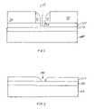
- FIG. 1shows a high-level diagram of a memory device of the present invention including a memory array and periphery circuitry formed on a substrate;
- FIG. 2Ashows a high-level diagram of a memory array of the present invention
- FIG. 2Bis a schematic diagram of a memory array of the present invention.
- FIG. 3is a schematic diagram of a memory cell incorporating a programmable resistance memory material
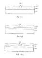
- FIGS. 4 through 11shows an embodiment of the process of the present invention for making a programmable resistance memory element with a tapered opening
- FIGS. 12A through 12Cshows examples of three pores having different degrees of taper made by the process of the present invention.
- the memory device 10is an integrated circuit memory formed on a semiconductor substrate 100 .
- the memory device 10includes a memory matrix or array 14 that includes a plurality of memory cells for storing data.
- the memory matrix 14is coupled to periphery circuitry 16 by the plurality of control lines 18 .
- the periphery circuitry 16may include circuitry for addressing the memory cells contained within the memory array 14 , along with circuitry for storing data in and retrieving data from the memory cells.
- the periphery circuitry 16may also include other circuitry used for controlling or otherwise insuring the proper functioning of the memory device 10 .
- FIG. 2AA top view of the memory array 14 is shown in FIG. 2A .
- the memory array 14includes a plurality of memory cells 20 that are arranged in generally perpendicular rows and columns.
- the memory cells 20 in each roware coupled together by a respective wordline 22
- the memory cells 20 in each columnare coupled together by a respective bitline 24 .
- each memory cell 20includes a wordline node 26 that is coupled to a respective wordline 22
- each memory cell 20includes a bitline node 28 that is coupled to a respective bitline 24 .
- the conductive wordlines 22 and bitlines 24are collectively referred to as address lines. These address lines are electrically coupled to the periphery circuitry 16 (shown in FIG. 1 ) so that each of the memory cells 20 can be accessed for the storage and retrieval of information.
- FIG. 3illustrates an exemplary memory cell 20 that may be used in the memory array 14 .
- the memory cell 20includes a memory element 30 which is coupled to an access device 32 .
- the access deviceelectrically isolates each memory element from all other memory elements in the array.
- the memory element 30is illustrated as a programmable resistive element, and the access device 32 is illustrated as a diode.
- the programmable resistive elementmay be made of a chalcogenide material, as will be more fully explained below.
- the memory element 30is coupled to a wordline 22
- the access device 32is coupled to a bitline 24 .
- connections of the memory element 20may be reversed without adversely affecting the operation of the memory array 14 .
- each memory cellis electrically isolated from other memory cells in the array in any suitable manner, such as by the addition of imbedded field oxide regions between each memory cell.
- a semiconductor substrate 100is provided.
- the substrate 100may include the access devices as well as the bitlines and/or wordlines.
- a layer 110is then deposited on top of the substrate 100 .
- the layer 110is preferably formed of a conductive material. Any conductive material may be used. Examples of the conductive materials which may be used include, but not limited to, titanium tungsten, titanium nitride, titanium aluminum nitride, titanium carbonitride, titanium silicon nitride, molybdenum, carbon, carbon silicide, tungsten silicide.
- the layer 110serves as a first electrode (in this case the bottom electrode) for the memory element.
- a layer 120is then formed over the layer 110 of conductive material.
- the layer 120is preferably formed of a dielectric material.
- the dielectric materialmay be any dielectric material, such as an oxide or a nitride.
- the oxidemay be silicon dioxide while the nitride may be silicon nitride.
- the dielectric materialis preferably silicon dioxide.
- the silicon dioxidemay be from a TEOS source.
- the layer 120 ofmay be formed in any suitable manner, such as by chemical vapor deposition (CVD).
- a layer 130is then formed over the dielectric layer 120 .
- the layer 130is preferably formed of polysilicon. (However, in other embodiments of the invention it is possible that layer 130 be formed of a dielectric material such as an oxide or a nitride).
- an opening 140is then formed through the polysilicon layer 130 so as to expose a portion of the underlying layer 120 of dielectric material.
- the opening 140may be any shape.
- the opening 140may be a hole.
- the holemay have any shape, and may, for example, be a substantially circular hole, a subtantially square hole, or a rectangular hole.
- the opening 140may be formed as a trench.
- the opening 140is formed as a substantially circular hole.
- the opening 140includes the sidewall surface 140 S about the periphery of the opening and the bottom surface 140 B. In the embodiment shown in FIG. 5 , the opening is a substantially circular hole.
- the openinghas a minimum lateral dimension X 1 (where the lateral dimension is a dimension parallel to the substrate).
- any suitable method of forming the opening 140may be used. For example, using standard photolithographic techniques, a hard mask (not shown) may be deposited on top of the layer 130 and patterned in the size and shape of the resulting opening 140 .
- the opening 140may be formed using a conventional contact hole mask.
- the opening 140may be formed so that its minimum lateral dimension is at or above the photolithographic limit. Presently, the photolithographic limit is greater than about 1000 Angstroms. In one embodiment, the opening 140 may have a minimum lateral dimension which is greater than about 1300 Angstroms.
- the opening 140is preferably formed so that the layer 120 is exposed.
- the opening 140does not extend into substantially any of layer 120 .
- a layer 150is then formed over the sidewall and bottom surfaces of the opening 140 .
- the layer 150is formed over the top surface of the layer 130 as well as over the sidewall surface 140 S and over the bottom surface 140 B of the opening 140 .
- the layer 150is preferably formed of the same material as layer 130 . (However, it is also possible that layer 150 be formed of a different material from layer 130 ).
- the layer 150is preferably formed of polysilicon. (In other embodiments of the invention, it is possible that the layer 150 , like layer 130 , may be formed of a dielectric material such as an oxide or a nitride).
- the deposition of layer 150is a substantially conformal deposition so that the layer 150 of polysilicon preferably has a substantially uniform thickness on the top surface of the layer 130 as well as on the sidewall surface 140 S and bottom surface 140 B. As shown, the layer 150 of polysilicon lines the sidewall and bottom surface of the opening 140 but does not fill the opening.
- the layer 150 of polysiliconincludes a sidewall layer portion that is formed on the sidewall surface 140 S of the opening 140 . It also includes a bottom layer portion that is formed on the bottom surface 140 B of the opening.
- the thickness chosen for the layer 150may be based on the minimum lateral dimension X 1 of the opening 140 .
- the thickness of layer 150may be chosen so that it is about one-third the minimum lateral dimension X 1 of the opening 140 .
- the thickness of the layer 150may be chosen to be about 1200 Angstroms or less.
- the thickness of the layer 150may be chosen to be about 500 Angstroms or less.
- Other thickness values for the layer 150are possible and the present invention is not limited to any particular thickness value or to any particular way of choosing the thickness value.
- the layer 150 of polysiliconis then anisotropically etched so as to remove the horizontally disposed portions of the layer 150 .
- the anisotropic etchremoves the horizontally disposed portion of layer 150 that is on the top surface of layer 130 . It also removes the horizontally disposed portion of layer 150 that is on the bottom surface 140 B of the opening 140 .
- the anisotropic etchleaves a portion of the layer 150 that is disposed on the sidewall surface 140 S.
- the portion of the layer 150 that remains after the anisotropic etchis a sidewall spacer 160 (as shown in FIG. 7 ) disposed on the sidewall surface 140 S.
- the sidewall spacer 160 of polysiliconis formed over the sidewall surface 140 S of the opening 140 . If the opening is in the form of a substantially circular hole, then the sidewall spacer 160 is cylindrically shaped (having two open ends).
- the bottom of sidewall spacer 160 shown in FIG. 7has a lateral thickness “t SPACER ”.
- the thickness of the bottom of the sidewall spacer 160is substantially equal to the thickness of the layer 150 (shown in FIG. 6 ) provided that the deposition of the layer 150 is a substantially conformal deposition and that the etch which removes the horizontally disposed portions of layer 150 is a substantially anisotropic etch.
- the sidewall spacer 160reduces the lateral cross-sectional dimension of opening 140 (shown in FIG. 5 ) so as to form a smaller second opening 170 (shown in FIG. 6 ). That is, the second opening 170 has a smaller lateral cross-sectional dimension than the opening 140 . Since the opening 140 may be sized to have a lateral cross-sectional dimension at the photolithographic limit, it is thus possible that the lateral cross-sectional dimension of the second opening 170 be less than the photolithographic limit. In one embodiment of the invention, the minimum lateral dimension of the second opening 170 may be less than about 1300 Angstroms, preferably less than about 1000 Angstroms, more preferably less than about 600 Angstroms, and most preferably less than about 400 Angstroms.
- the remaining portion of layer 130 of polysilicon in combination with sidewall spacer 160 of polysiliconforms a mask overlying a portion of the layer 120 of dielectric material. That portion of the layer 120 which is exposed is the portion of the layer 120 which is directly underneath the smaller opening 170 and which is thus not covered by the layer 130 or spacer 160 of polysilicon.
- the exposed portion of the layer 120 that is underlying the smaller opening 170is then etched.
- the etching technique usedis preferably an anisotropic etch.
- the etching processremoves a sufficient amount of the dielectric layer 120 to form a recess 180 in the dielectric layer 120 .
- the etchstops short of forming a complete opening through the dielectric layer 120 . That is, the etch stops short of exposing the underlying layer 110 .
- the etch of the dielectric layer 120creates a recess having a depth “d”.
- the etching step that forms the recess 180is referred to herein as the “recess forming etch”.
- the layer 130 of polysilicon as well as the sidewall spacer 160 of polysiliconare then removed.
- the removal of the layer 130 as well as the sidewall spacer 160is referred to as the “strip step”.
- the polysilicon materialis preferably removed by using a dry etch process.
- the same dry etch process that is used to remove the polysilicon material of layer 130 and spacer 160also etches the underlying dielectric material of layer 120 . That is, the dry etch process etches (1) the polysilicon material of layer 130 and spacer 160 , and (2) the dielectric material of layer 120 .
- the two different materialsare preferably etched at different rates.
- the etch processis chosen so that the etch rate r 1 of the polysilicon material of layer 130 and spacer 160 is greater than the etch rate r 2 of the dielectric material of layer 120 .
- the etch processis chosen so that the etch rate of the layer 110 (preferably formed of a conductive material) is negligible.
- the ratio of the etch rate r 1 to the etch rate r 2forms an etch rate ratio R. That is, the etch rate r 1 divided by etch rate r 2 provides an etch rate ratio R.
- the etching process of the strip stepetches the recess 175 so that an opening 180 is formed (as shown in FIG. 9 ) that extends through the dielectric layer 120 and exposes the conductive layer 110 .
- the opening 180is preferably in the form of a hole.
- a holeis also referred to as a pore.
- the pore 180preferably has a substantially circular cross section.
- the minimum lateral cross-sectional dimension of the pore 180is preferably less than 1000 Angstroms, more preferably less than 600 Angstroms and more preferably less than 400 Angstroms.
- FIGS. 12A–12CExamples of pore contours are shown in FIGS. 12A–12C .
- the method of the present inventionprovides a way to control the contour of the sidewall surface of an opening such as a hole (also referred to as a pore) or a trench.
- the pore 180may be made to taper so that the slope of the sidewall surface of the pore 180 becomes less and less vertical in the direction from the bottom of the pore to the top of the pore.
- the minimum lateral cross-sectional dimensionis larger at the top of the pore than at the bottom of the pore.
- the tapering of the poreallows for improved step coverage of the material (such as a programmable resistance material) sputtered into the pore.
- the slope of a bottom portion of the sidewall surface of the poremay be kept substantially vertical to allow for better control of the area of the exposed underlying conductive layer 110 (e.g. the bottom electrode of the memory element).
- the exposed surface of the conductive layer 110is preferably not a strong function of etch time in the strip process.
- the method of the present inventionis applicable to all types of openings, including holes (of all cross-sectional shapes) as well as trenches.
- the present inventionmay be used to control the contour of all types of openings, including holes (of all cross-sectional shapes) as well as trenches.
- the material of layer 120is a dielectric material formed of TEOS oxide
- the material of layer 110is a conductive material formed of TiAlN
- an SF 6 /N 2 etch chemistrymay be used during the strip step. This etch chemistry has a negligible etch rate of the TiAlN.
- a specific example of an etch rate ratio Ris an etch rate ratio of about 5.
- the recess 175is formed that has a depth d.
- the recess 175is formed so that the ratio of the depth d of the recess 175 to the thickness of the layer 120 is preferably less than about 0.75, more preferably less than about 0.5, and most preferably less than about 0.4.
- the ratio of the depth d of the recess 175 to the thickness of the layer 120may be less than 0.35. In one embodiment of the invention, the ratio of the depth d of the recess 175 to the thickness of the layer 120 is about 1 ⁇ 3 (one-third).
- a layer of programmable resistance memory material 190(preferably a phase-change material and more preferably a chalcogenide material) is then deposited over the dielectric layer 120 and into the pore 180 .
- the memory material 190fills the pore 180 .
- the memory materialmay be deposited by methods such as sputtering, evaporation or chemical vapor deposition.
- a layer 195is then deposited over the memory material 190 to form an upper electrode for the memory element.
- the layer 195is formed of a conductive material.
- the conductive material that is used to form the upper electrode 195may be formed of the same conductive materials used to form the bottom electrode 110 .
- Examples of a conductive materials that may be used for the upper electrode 195include titanium tungsten, carbon and titanium nitride.
- layer 110may be utilized for layer 110 , layer 120 , layer 130 , and spacer 160 .
- Spacer 160is formed by etching the layer 150 shown in FIG. 6 ).
- layer 130 and spacer 160may be formed of polysilicon while layer 120 may be formed of a dielectric such as an oxide or a nitride.
- layer 130 and spacer 160be formed of a dielectric material such as an oxide or a nitride.
- the oxidemay be silicon oxide while the nitride may be silicon nitride).
- layer 130 and spacer 160may be formed of a nitride while the layer 120 may be formed of an oxide.
- layer 130 and spacer 160may be formed of an oxide while layer 120 may be formed of a nitride. Examples of possible combinations of materials are provided in the table below. The invention is not limited to the examples provided in the table below.
- the etch processbe chosen so that the etch rate r 1 of the material of layer 130 and spacer 160 be greater than the etch rate r 2 of the material of layer 120 .
- a specific example of an etch rate ratiois an etch rate ratio R of about 5.
- layer 130 and spacer 160be formed of the same material, it is also possible that the layer 130 be formed of a material which is different from spacer 160 .
- layer 130may be formed of one type of oxide while spacer 160 may be formed of another type of oxide.
- the etching processbe chosen so that etch rate of layer 130 be greater than the etch rate of layer 120 .
- the etching processbe chosen so that etch rate of spacer 160 also be greater than the etch rate of layer 120 .
- the etch rate ratio of the etch rate of layer 130 to the etch rate of layer 120is preferably between 2 and 100, more preferably between 2 and 50, and most preferably between 2 and 10. In one embodiment, the etch rate ratio of layer 130 to layer 120 may be between 4 and 6. A specific example of an etch rate ratio of layer 130 to layer 120 is an etch rate ratio of about 5. Likewise, the etch rate ratio of the etch rate of spacer 160 to the etch rate of layer 120 is also preferably between 2 and 100, more preferably between 2 and 50, and most preferably between 2 and 10. In one embodiment, the etch rate ratio of spacer 160 to layer 120 may be between 4 and 6. A specific example of an etch rate ratio of spacer 160 to layer 120 is an etch rate ratio of about 5.
- layer 110be a conductive material
- layer 110be formed of a material other than a conductive material.
- the method of the present inventionbe used to form an opening (such as a pore) that overlies and exposes a layer formed from a material that is not a conductive material.
- the particular materials selected for each of the layers 110 , 120 , 130 and 150will be selected to provide proper selectivity during the various etching processes as will be recognized by persons of ordinary skill in the art.
- the memory elements of the present inventionmay be electrically coupled to isolation/selection devices and to addressing lines in order to form a memory array.
- the isolation/addressing devicespermit each discrete memory cell to be read and written to without interfering with information stored in adjacent or remote memory cells of the array.
- the present inventionis not limited to the use of any specific type of isolation/addressing device.
- isolation/addressing devicesinclude field-effect transistors, bipolar junction transistors, and diodes.
- Examples of field-effect transistorsinclude JFET and MOSFET.
- Examples of MOSFETinclude NMOS transistors and PMOS transistors.
- NMOS and PMOSmay even be formed on the same chip for CMOS technologies.
- isolation/addressing deviceassociated with each memory element of a memory array structure is isolation/addressing device which serves as an isolation/addressing device for that memory element thereby enabling that cell to be read and written without interfering with information stored in other adjacent or remote memory elements of the array.
- the memory element of the present inventioncomprises a volume of memory material.
- the volume of memory materialis a programmable resistance memory material which is programmable to at least a first resistance state and a second resistance state.
- the memory materialis preferably programmed in response to electrical signals.
- the electrical signals used to program the materialsare electrical currents which are directed to the memory material.
- the memory materialis programmable to two resistance states so that each of the memory elements is capable of storing a single bit of information. In another embodiment, the memory material is programmable to at least three resistance states so that each of the memory elements is capable of storing more than one bit of information. In yet another embodiment, the memory material is programmable to at least four resistance states so that each of the memory elements is capable of storing at least two bits of information.
- the memory materialsmay have a range of resistance values providing for the gray scale storage of multiple bits of information.
- the memory materialsmay be directly overwritable so that they can be programmed from any of their resistance states to any other of their resistance states without first having to be set to a starting state.
- the same programming pulse or pulsesmay be used to program the memory material to a specific resistance state regardless of its previous resistance state.
- the same current pulse or pulsesmay be used to program the material to its high resistance state regardless of its previous state.
- the memory materialmay be a phase change material.
- the phase-change materialsmay be any phase change memory material known in the art.
- the phase change materialsare capable of exhibiting a first order phase transition. Examples of materials are described in U.S. Pat. Nos. 5,166,758, 5,296,716, 5,414,271, 5,359,205, 5,341,328, 5,536,947, 5,534,712, 5,687,112, and 5,825,046 the disclosures of which are all incorporated by reference herein.
- the phase change materialsmay be formed from a plurality of atomic elements.
- the memory materialincludes at least one chalcogen element.
- the chalcogen elementmay be chosen from the group consisting of Te, Se, and mixtures or alloys thereof.
- the memory materialmay further include at least one element selected from the group consisting of Ge, Sb, Bi, Pb, Sn, As, S, Si, P, O, and mixtures or alloys thereof.
- the memory materialcomprises the elements Te, Ge and Sb.
- the memory materialconsists essentially of Te, Ge and Sb.
- the memory materialmay include at least one transition metal element.
- transition metalas used herein includes elements 21 to 30 , 39 to 48 , 57 and 72 to 80 .
- the one or more transition metal elementsare selected from the group consisting of Cr, Fe, Ni, Nb, Pd, Pt and mixtures or alloys thereof.
- the memory materials which include transition metalsmay be elementally modified forms of the memory materials in the Te—Ge—Sb ternary system. This elemental modification may be achieved by the incorporation of transition metals into the basic Te—Ge—Sb ternary system, with or without an additional chalcogen element, such as Se.
- a first example of an elementally modified memory materialis a phase-change memory material which includes Te, Ge, Sb and a transition metal, in the ratio (Te a Ge b Sb 100 ⁇ (a+b) ) c TM 100 ⁇ c where the subscripts are in atomic percentages which total 100% of the constituent elements, wherein TM is one or more transition metals, a and b are as set forth herein above for the basic Te—Ge—Sb ternary system and c is between about 90% and about 99.99%.
- the transition metalmay include Cr, Fe, Ni, Nb, Pd, Pt and mixtures or alloys thereof.
- a second example of an elementally modified memory materialis a phase-change memory material which includes Te, Ge, Sb, Se and a transition metal, in the ratio (Te a Ge b Sb 100 ⁇ (a+b) ) c TM d Se 100 ⁇ (c+d) where the subscripts are in atomic percentages which total 100% of the constituent elements, TM is one or more transition metals, a and b are as set forth hereinabove for the basic Te—Ge—Sb ternary system, c is between about 90% and 99.5% and d is between about 0.01% and 10%.
- the transition metalmay include Cr, Fe, Ni, Pd, Pt, Nb, and mixtures or alloys thereof.
Landscapes
- Engineering & Computer Science (AREA)
- Manufacturing & Machinery (AREA)
- Semiconductor Memories (AREA)
Abstract
Description
| layer | |||||
| 120 | |||||
| combination 1 | oxide | polysilicon | polysilicon | ||
| combination 2 | nitride | polysilicon | polysilicon | ||
| combination 3 | oxide | nitride | nitride | ||
| combination 4 | nitride | oxide | oxide | ||
Claims (41)
Priority Applications (3)
| Application Number | Priority Date | Filing Date | Title |
|---|---|---|---|
| US10/396,587US7045383B2 (en) | 2001-09-19 | 2003-03-24 | Method for making tapered opening for programmable resistance memory element |
| PCT/US2004/008633WO2004086459A2 (en) | 2003-03-24 | 2004-03-22 | Method for making tapered opening for programmable resistance memory element |
| US11/434,383US20060205108A1 (en) | 2001-09-19 | 2006-05-15 | Method for making tapered opening for programmable resistance memory element |
Applications Claiming Priority (2)
| Application Number | Priority Date | Filing Date | Title |
|---|---|---|---|
| US09/955,408US6613604B2 (en) | 2001-08-02 | 2001-09-19 | Method for making small pore for use in programmable resistance memory element |
| US10/396,587US7045383B2 (en) | 2001-09-19 | 2003-03-24 | Method for making tapered opening for programmable resistance memory element |
Related Parent Applications (1)
| Application Number | Title | Priority Date | Filing Date |
|---|---|---|---|
| US09/955,408Continuation-In-PartUS6613604B2 (en) | 2001-06-26 | 2001-09-19 | Method for making small pore for use in programmable resistance memory element |
Related Child Applications (1)
| Application Number | Title | Priority Date | Filing Date |
|---|---|---|---|
| US11/434,383ContinuationUS20060205108A1 (en) | 2001-09-19 | 2006-05-15 | Method for making tapered opening for programmable resistance memory element |
Publications (2)
| Publication Number | Publication Date |
|---|---|
| US20030215978A1 US20030215978A1 (en) | 2003-11-20 |
| US7045383B2true US7045383B2 (en) | 2006-05-16 |
Family
ID=33096795
Family Applications (2)
| Application Number | Title | Priority Date | Filing Date |
|---|---|---|---|
| US10/396,587Expired - LifetimeUS7045383B2 (en) | 2001-09-19 | 2003-03-24 | Method for making tapered opening for programmable resistance memory element |
| US11/434,383AbandonedUS20060205108A1 (en) | 2001-09-19 | 2006-05-15 | Method for making tapered opening for programmable resistance memory element |
Family Applications After (1)
| Application Number | Title | Priority Date | Filing Date |
|---|---|---|---|
| US11/434,383AbandonedUS20060205108A1 (en) | 2001-09-19 | 2006-05-15 | Method for making tapered opening for programmable resistance memory element |
Country Status (2)
| Country | Link |
|---|---|
| US (2) | US7045383B2 (en) |
| WO (1) | WO2004086459A2 (en) |
Cited By (4)
| Publication number | Priority date | Publication date | Assignee | Title |
|---|---|---|---|---|
| US20060226409A1 (en)* | 2005-04-06 | 2006-10-12 | International Business Machines Corporation | Structure for confining the switching current in phase memory (PCM) cells |
| US20090231911A1 (en)* | 2008-03-14 | 2009-09-17 | Micron Technology, Inc. | Phase change memory cell with constriction structure |
| US20120051124A1 (en)* | 2010-08-31 | 2012-03-01 | Micron Technology, Inc. | Phase change memory structures and methods |
| US8158476B2 (en) | 2005-03-28 | 2012-04-17 | Micron Technology, Inc. | Integrated circuit fabrication |
Families Citing this family (123)
| Publication number | Priority date | Publication date | Assignee | Title |
|---|---|---|---|---|
| US7109056B2 (en)* | 2001-09-20 | 2006-09-19 | Micron Technology, Inc. | Electro-and electroless plating of metal in the manufacture of PCRAM devices |
| DE10340405B3 (en)* | 2003-09-02 | 2004-12-23 | Infineon Technologies Ag | Integrated semiconductor memory with selective reduction of effective bit line length for reducing current requirement by partial disconnection of second bit line section from first bit line section |
| DE102004031742A1 (en)* | 2004-06-30 | 2006-01-19 | Infineon Technologies Ag | Production of a sub-lithographic contact structure of a memory cell in a semiconductor component comprises preparing a front-end-of-line semiconductor wafer with an electrical contact, depositing an insulating layer and further processing |
| KR100629367B1 (en) | 2004-07-22 | 2006-09-29 | 삼성전자주식회사 | Via hole formation method and method for manufacturing phase change memory device using the same |
| US7151040B2 (en)* | 2004-08-31 | 2006-12-19 | Micron Technology, Inc. | Methods for increasing photo alignment margins |
| US7910288B2 (en) | 2004-09-01 | 2011-03-22 | Micron Technology, Inc. | Mask material conversion |
| US7655387B2 (en) | 2004-09-02 | 2010-02-02 | Micron Technology, Inc. | Method to align mask patterns |
| US7115525B2 (en)* | 2004-09-02 | 2006-10-03 | Micron Technology, Inc. | Method for integrated circuit fabrication using pitch multiplication |
| US7253118B2 (en) | 2005-03-15 | 2007-08-07 | Micron Technology, Inc. | Pitch reduced patterns relative to photolithography features |
| US7390746B2 (en)* | 2005-03-15 | 2008-06-24 | Micron Technology, Inc. | Multiple deposition for integration of spacers in pitch multiplication process |
| DE102005012047A1 (en)* | 2005-03-16 | 2006-09-28 | Infineon Technologies Ag | Solid-state electrolyte memory manufacture involves coating first electrode with solid-state electrolyte layer, and then forming second electrode on solid-state electrolyte layer |
| US7429536B2 (en) | 2005-05-23 | 2008-09-30 | Micron Technology, Inc. | Methods for forming arrays of small, closely spaced features |
| US7560390B2 (en) | 2005-06-02 | 2009-07-14 | Micron Technology, Inc. | Multiple spacer steps for pitch multiplication |
| US7396781B2 (en) | 2005-06-09 | 2008-07-08 | Micron Technology, Inc. | Method and apparatus for adjusting feature size and position |
| US7696503B2 (en)* | 2005-06-17 | 2010-04-13 | Macronix International Co., Ltd. | Multi-level memory cell having phase change element and asymmetrical thermal boundary |
| US8237140B2 (en) | 2005-06-17 | 2012-08-07 | Macronix International Co., Ltd. | Self-aligned, embedded phase change RAM |
| US7413981B2 (en) | 2005-07-29 | 2008-08-19 | Micron Technology, Inc. | Pitch doubled circuit layout |
| US8123968B2 (en) | 2005-08-25 | 2012-02-28 | Round Rock Research, Llc | Multiple deposition for integration of spacers in pitch multiplication process |
| US7816262B2 (en) | 2005-08-30 | 2010-10-19 | Micron Technology, Inc. | Method and algorithm for random half pitched interconnect layout with constant spacing |
| US7829262B2 (en) | 2005-08-31 | 2010-11-09 | Micron Technology, Inc. | Method of forming pitch multipled contacts |
| US7759197B2 (en)* | 2005-09-01 | 2010-07-20 | Micron Technology, Inc. | Method of forming isolated features using pitch multiplication |
| US7776744B2 (en) | 2005-09-01 | 2010-08-17 | Micron Technology, Inc. | Pitch multiplication spacers and methods of forming the same |
| US7393789B2 (en) | 2005-09-01 | 2008-07-01 | Micron Technology, Inc. | Protective coating for planarization |
| US7572572B2 (en) | 2005-09-01 | 2009-08-11 | Micron Technology, Inc. | Methods for forming arrays of small, closely spaced features |
| US7786460B2 (en) | 2005-11-15 | 2010-08-31 | Macronix International Co., Ltd. | Phase change memory device and manufacturing method |
| US7635855B2 (en) | 2005-11-15 | 2009-12-22 | Macronix International Co., Ltd. | I-shaped phase change memory cell |
| US7449710B2 (en) | 2005-11-21 | 2008-11-11 | Macronix International Co., Ltd. | Vacuum jacket for phase change memory element |
| US7599217B2 (en) | 2005-11-22 | 2009-10-06 | Macronix International Co., Ltd. | Memory cell device and manufacturing method |
| US7459717B2 (en) | 2005-11-28 | 2008-12-02 | Macronix International Co., Ltd. | Phase change memory cell and manufacturing method |
| US7688619B2 (en)* | 2005-11-28 | 2010-03-30 | Macronix International Co., Ltd. | Phase change memory cell and manufacturing method |
| US7531825B2 (en) | 2005-12-27 | 2009-05-12 | Macronix International Co., Ltd. | Method for forming self-aligned thermal isolation cell for a variable resistance memory array |
| US8062833B2 (en) | 2005-12-30 | 2011-11-22 | Macronix International Co., Ltd. | Chalcogenide layer etching method |
| US7741636B2 (en) | 2006-01-09 | 2010-06-22 | Macronix International Co., Ltd. | Programmable resistive RAM and manufacturing method |
| US7560337B2 (en) | 2006-01-09 | 2009-07-14 | Macronix International Co., Ltd. | Programmable resistive RAM and manufacturing method |
| US20070200202A1 (en)* | 2006-02-28 | 2007-08-30 | International Business Machines Corporation | Phase change memory structure having an electrically formed constriction |
| US7842558B2 (en) | 2006-03-02 | 2010-11-30 | Micron Technology, Inc. | Masking process for simultaneously patterning separate regions |
| US7902074B2 (en) | 2006-04-07 | 2011-03-08 | Micron Technology, Inc. | Simplified pitch doubling process flow |
| US8003310B2 (en)* | 2006-04-24 | 2011-08-23 | Micron Technology, Inc. | Masking techniques and templates for dense semiconductor fabrication |
| US7488685B2 (en) | 2006-04-25 | 2009-02-10 | Micron Technology, Inc. | Process for improving critical dimension uniformity of integrated circuit arrays |
| US7608848B2 (en) | 2006-05-09 | 2009-10-27 | Macronix International Co., Ltd. | Bridge resistance random access memory device with a singular contact structure |
| US7732800B2 (en)* | 2006-05-30 | 2010-06-08 | Macronix International Co., Ltd. | Resistor random access memory cell with L-shaped electrode |
| US7795149B2 (en) | 2006-06-01 | 2010-09-14 | Micron Technology, Inc. | Masking techniques and contact imprint reticles for dense semiconductor fabrication |
| US7723009B2 (en) | 2006-06-02 | 2010-05-25 | Micron Technology, Inc. | Topography based patterning |
| US7785920B2 (en) | 2006-07-12 | 2010-08-31 | Macronix International Co., Ltd. | Method for making a pillar-type phase change memory element |
| US7611980B2 (en) | 2006-08-30 | 2009-11-03 | Micron Technology, Inc. | Single spacer process for multiplying pitch by a factor greater than two and related intermediate IC structures |
| US7666578B2 (en) | 2006-09-14 | 2010-02-23 | Micron Technology, Inc. | Efficient pitch multiplication process |
| US7504653B2 (en) | 2006-10-04 | 2009-03-17 | Macronix International Co., Ltd. | Memory cell device with circumferentially-extending memory element |
| US7510929B2 (en)* | 2006-10-18 | 2009-03-31 | Macronix International Co., Ltd. | Method for making memory cell device |
| US7863655B2 (en) | 2006-10-24 | 2011-01-04 | Macronix International Co., Ltd. | Phase change memory cells with dual access devices |
| US7476587B2 (en) | 2006-12-06 | 2009-01-13 | Macronix International Co., Ltd. | Method for making a self-converged memory material element for memory cell |
| US7903447B2 (en) | 2006-12-13 | 2011-03-08 | Macronix International Co., Ltd. | Method, apparatus and computer program product for read before programming process on programmable resistive memory cell |
| US7718989B2 (en) | 2006-12-28 | 2010-05-18 | Macronix International Co., Ltd. | Resistor random access memory cell device |
| US8138028B2 (en) | 2007-02-12 | 2012-03-20 | Macronix International Co., Ltd | Method for manufacturing a phase change memory device with pillar bottom electrode |
| US7956344B2 (en) | 2007-02-27 | 2011-06-07 | Macronix International Co., Ltd. | Memory cell with memory element contacting ring-shaped upper end of bottom electrode |
| US7786461B2 (en) | 2007-04-03 | 2010-08-31 | Macronix International Co., Ltd. | Memory structure with reduced-size memory element between memory material portions |
| US7569844B2 (en)* | 2007-04-17 | 2009-08-04 | Macronix International Co., Ltd. | Memory cell sidewall contacting side electrode |
| US7923373B2 (en) | 2007-06-04 | 2011-04-12 | Micron Technology, Inc. | Pitch multiplication using self-assembling materials |
| US8563229B2 (en) | 2007-07-31 | 2013-10-22 | Micron Technology, Inc. | Process of semiconductor fabrication with mask overlay on pitch multiplied features and associated structures |
| US7729161B2 (en) | 2007-08-02 | 2010-06-01 | Macronix International Co., Ltd. | Phase change memory with dual word lines and source lines and method of operating same |
| US8178386B2 (en) | 2007-09-14 | 2012-05-15 | Macronix International Co., Ltd. | Phase change memory cell array with self-converged bottom electrode and method for manufacturing |
| US7919766B2 (en) | 2007-10-22 | 2011-04-05 | Macronix International Co., Ltd. | Method for making self aligning pillar memory cell device |
| US7737039B2 (en) | 2007-11-01 | 2010-06-15 | Micron Technology, Inc. | Spacer process for on pitch contacts and related structures |
| US7659208B2 (en) | 2007-12-06 | 2010-02-09 | Micron Technology, Inc | Method for forming high density patterns |
| US7790531B2 (en) | 2007-12-18 | 2010-09-07 | Micron Technology, Inc. | Methods for isolating portions of a loop of pitch-multiplied material and related structures |
| US8158965B2 (en)* | 2008-02-05 | 2012-04-17 | Macronix International Co., Ltd. | Heating center PCRAM structure and methods for making |
| US8030218B2 (en)* | 2008-03-21 | 2011-10-04 | Micron Technology, Inc. | Method for selectively modifying spacing between pitch multiplied structures |
| US8084842B2 (en) | 2008-03-25 | 2011-12-27 | Macronix International Co., Ltd. | Thermally stabilized electrode structure |
| US8030634B2 (en)* | 2008-03-31 | 2011-10-04 | Macronix International Co., Ltd. | Memory array with diode driver and method for fabricating the same |
| US7825398B2 (en) | 2008-04-07 | 2010-11-02 | Macronix International Co., Ltd. | Memory cell having improved mechanical stability |
| US7791057B2 (en) | 2008-04-22 | 2010-09-07 | Macronix International Co., Ltd. | Memory cell having a buried phase change region and method for fabricating the same |
| US8077505B2 (en) | 2008-05-07 | 2011-12-13 | Macronix International Co., Ltd. | Bipolar switching of phase change device |
| US7701750B2 (en) | 2008-05-08 | 2010-04-20 | Macronix International Co., Ltd. | Phase change device having two or more substantial amorphous regions in high resistance state |
| US8415651B2 (en) | 2008-06-12 | 2013-04-09 | Macronix International Co., Ltd. | Phase change memory cell having top and bottom sidewall contacts |
| US8134857B2 (en) | 2008-06-27 | 2012-03-13 | Macronix International Co., Ltd. | Methods for high speed reading operation of phase change memory and device employing same |
| US8076208B2 (en)* | 2008-07-03 | 2011-12-13 | Micron Technology, Inc. | Method for forming transistor with high breakdown voltage using pitch multiplication technique |
| US7932506B2 (en) | 2008-07-22 | 2011-04-26 | Macronix International Co., Ltd. | Fully self-aligned pore-type memory cell having diode access device |
| US7903457B2 (en) | 2008-08-19 | 2011-03-08 | Macronix International Co., Ltd. | Multiple phase change materials in an integrated circuit for system on a chip application |
| US7719913B2 (en) | 2008-09-12 | 2010-05-18 | Macronix International Co., Ltd. | Sensing circuit for PCRAM applications |
| US8324605B2 (en) | 2008-10-02 | 2012-12-04 | Macronix International Co., Ltd. | Dielectric mesh isolated phase change structure for phase change memory |
| US7897954B2 (en) | 2008-10-10 | 2011-03-01 | Macronix International Co., Ltd. | Dielectric-sandwiched pillar memory device |
| US8036014B2 (en) | 2008-11-06 | 2011-10-11 | Macronix International Co., Ltd. | Phase change memory program method without over-reset |
| US8664689B2 (en)* | 2008-11-07 | 2014-03-04 | Macronix International Co., Ltd. | Memory cell access device having a pn-junction with polycrystalline plug and single-crystal semiconductor regions |
| US8907316B2 (en) | 2008-11-07 | 2014-12-09 | Macronix International Co., Ltd. | Memory cell access device having a pn-junction with polycrystalline and single crystal semiconductor regions |
| US8492282B2 (en) | 2008-11-24 | 2013-07-23 | Micron Technology, Inc. | Methods of forming a masking pattern for integrated circuits |
| US7869270B2 (en) | 2008-12-29 | 2011-01-11 | Macronix International Co., Ltd. | Set algorithm for phase change memory cell |
| US8089137B2 (en) | 2009-01-07 | 2012-01-03 | Macronix International Co., Ltd. | Integrated circuit memory with single crystal silicon on silicide driver and manufacturing method |
| US8107283B2 (en) | 2009-01-12 | 2012-01-31 | Macronix International Co., Ltd. | Method for setting PCRAM devices |
| US8030635B2 (en) | 2009-01-13 | 2011-10-04 | Macronix International Co., Ltd. | Polysilicon plug bipolar transistor for phase change memory |
| US8064247B2 (en) | 2009-01-14 | 2011-11-22 | Macronix International Co., Ltd. | Rewritable memory device based on segregation/re-absorption |
| US8933536B2 (en) | 2009-01-22 | 2015-01-13 | Macronix International Co., Ltd. | Polysilicon pillar bipolar transistor with self-aligned memory element |
| US8084760B2 (en)* | 2009-04-20 | 2011-12-27 | Macronix International Co., Ltd. | Ring-shaped electrode and manufacturing method for same |
| US8173987B2 (en) | 2009-04-27 | 2012-05-08 | Macronix International Co., Ltd. | Integrated circuit 3D phase change memory array and manufacturing method |
| US8829646B2 (en)* | 2009-04-27 | 2014-09-09 | Macronix International Co., Ltd. | Integrated circuit 3D memory array and manufacturing method |
| US8097871B2 (en) | 2009-04-30 | 2012-01-17 | Macronix International Co., Ltd. | Low operational current phase change memory structures |
| US7933139B2 (en) | 2009-05-15 | 2011-04-26 | Macronix International Co., Ltd. | One-transistor, one-resistor, one-capacitor phase change memory |
| US7968876B2 (en) | 2009-05-22 | 2011-06-28 | Macronix International Co., Ltd. | Phase change memory cell having vertical channel access transistor |
| US8350316B2 (en)* | 2009-05-22 | 2013-01-08 | Macronix International Co., Ltd. | Phase change memory cells having vertical channel access transistor and memory plane |
| US8809829B2 (en) | 2009-06-15 | 2014-08-19 | Macronix International Co., Ltd. | Phase change memory having stabilized microstructure and manufacturing method |
| US8406033B2 (en) | 2009-06-22 | 2013-03-26 | Macronix International Co., Ltd. | Memory device and method for sensing and fixing margin cells |
| US8238149B2 (en) | 2009-06-25 | 2012-08-07 | Macronix International Co., Ltd. | Methods and apparatus for reducing defect bits in phase change memory |
| US8363463B2 (en) | 2009-06-25 | 2013-01-29 | Macronix International Co., Ltd. | Phase change memory having one or more non-constant doping profiles |
| US8198619B2 (en) | 2009-07-15 | 2012-06-12 | Macronix International Co., Ltd. | Phase change memory cell structure |
| US8110822B2 (en) | 2009-07-15 | 2012-02-07 | Macronix International Co., Ltd. | Thermal protect PCRAM structure and methods for making |
| US7894254B2 (en) | 2009-07-15 | 2011-02-22 | Macronix International Co., Ltd. | Refresh circuitry for phase change memory |
| JP2011066135A (en)* | 2009-09-16 | 2011-03-31 | Elpida Memory Inc | Method for fabricating phase-change memory device |
| US8064248B2 (en) | 2009-09-17 | 2011-11-22 | Macronix International Co., Ltd. | 2T2R-1T1R mix mode phase change memory array |
| US8178387B2 (en) | 2009-10-23 | 2012-05-15 | Macronix International Co., Ltd. | Methods for reducing recrystallization time for a phase change material |
| US8729521B2 (en) | 2010-05-12 | 2014-05-20 | Macronix International Co., Ltd. | Self aligned fin-type programmable memory cell |
| US8310864B2 (en) | 2010-06-15 | 2012-11-13 | Macronix International Co., Ltd. | Self-aligned bit line under word line memory array |
| US8507353B2 (en) | 2010-08-11 | 2013-08-13 | Samsung Electronics Co., Ltd. | Method of forming semiconductor device having self-aligned plug |
| US9082954B2 (en) | 2010-09-24 | 2015-07-14 | Macronix International Co., Ltd. | PCRAM with current flowing laterally relative to axis defined by electrodes |
| US8395935B2 (en) | 2010-10-06 | 2013-03-12 | Macronix International Co., Ltd. | Cross-point self-aligned reduced cell size phase change memory |
| US8497705B2 (en) | 2010-11-09 | 2013-07-30 | Macronix International Co., Ltd. | Phase change device for interconnection of programmable logic device |
| US8467238B2 (en) | 2010-11-15 | 2013-06-18 | Macronix International Co., Ltd. | Dynamic pulse operation for phase change memory |
| US8497182B2 (en) | 2011-04-19 | 2013-07-30 | Macronix International Co., Ltd. | Sidewall thin film electrode with self-aligned top electrode and programmable resistance memory |
| US8987700B2 (en) | 2011-12-02 | 2015-03-24 | Macronix International Co., Ltd. | Thermally confined electrode for programmable resistance memory |
| US8981330B2 (en) | 2012-07-16 | 2015-03-17 | Macronix International Co., Ltd. | Thermally-confined spacer PCM cells |
| US9214351B2 (en) | 2013-03-12 | 2015-12-15 | Macronix International Co., Ltd. | Memory architecture of thin film 3D array |
| US8916414B2 (en) | 2013-03-13 | 2014-12-23 | Macronix International Co., Ltd. | Method for making memory cell by melting phase change material in confined space |
| US9336879B2 (en) | 2014-01-24 | 2016-05-10 | Macronix International Co., Ltd. | Multiple phase change materials in an integrated circuit for system on a chip application |
| US9559113B2 (en) | 2014-05-01 | 2017-01-31 | Macronix International Co., Ltd. | SSL/GSL gate oxide in 3D vertical channel NAND |
| US9672906B2 (en) | 2015-06-19 | 2017-06-06 | Macronix International Co., Ltd. | Phase change memory with inter-granular switching |
| US9793323B1 (en) | 2016-07-11 | 2017-10-17 | Macronix International Co., Ltd. | Phase change memory with high endurance |
Citations (2)
| Publication number | Priority date | Publication date | Assignee | Title |
|---|---|---|---|---|
| US5814527A (en)* | 1996-07-22 | 1998-09-29 | Micron Technology, Inc. | Method of making small pores defined by a disposable internal spacer for use in chalcogenide memories |
| US5942803A (en)* | 1996-03-19 | 1999-08-24 | Samsung Electronics Co., Ltd. | Methods for forming openings with improved aspect ratios in integrated circuit devices, and related structures |
- 2003
- 2003-03-24USUS10/396,587patent/US7045383B2/ennot_activeExpired - Lifetime
- 2004
- 2004-03-22WOPCT/US2004/008633patent/WO2004086459A2/enactiveApplication Filing
- 2006
- 2006-05-15USUS11/434,383patent/US20060205108A1/ennot_activeAbandoned
Patent Citations (2)
| Publication number | Priority date | Publication date | Assignee | Title |
|---|---|---|---|---|
| US5942803A (en)* | 1996-03-19 | 1999-08-24 | Samsung Electronics Co., Ltd. | Methods for forming openings with improved aspect ratios in integrated circuit devices, and related structures |
| US5814527A (en)* | 1996-07-22 | 1998-09-29 | Micron Technology, Inc. | Method of making small pores defined by a disposable internal spacer for use in chalcogenide memories |
Cited By (23)
| Publication number | Priority date | Publication date | Assignee | Title |
|---|---|---|---|---|
| US8507341B2 (en) | 2005-03-28 | 2013-08-13 | Micron Technology, Inc. | Integrated circuit fabrication |
| US9412594B2 (en) | 2005-03-28 | 2016-08-09 | Micron Technology, Inc. | Integrated circuit fabrication |
| US9147608B2 (en) | 2005-03-28 | 2015-09-29 | Micron Technology, Inc. | Integrated circuit fabrication |
| US8859362B2 (en) | 2005-03-28 | 2014-10-14 | Micron Technology, Inc. | Integrated circuit fabrication |
| US8158476B2 (en) | 2005-03-28 | 2012-04-17 | Micron Technology, Inc. | Integrated circuit fabrication |
| US7488967B2 (en)* | 2005-04-06 | 2009-02-10 | International Business Machines Corporation | Structure for confining the switching current in phase memory (PCM) cells |
| US20060226409A1 (en)* | 2005-04-06 | 2006-10-12 | International Business Machines Corporation | Structure for confining the switching current in phase memory (PCM) cells |
| US9281478B2 (en) | 2008-03-14 | 2016-03-08 | Micron Technology, Inc. | Phase change memory cell with constriction structure |
| US20090231911A1 (en)* | 2008-03-14 | 2009-09-17 | Micron Technology, Inc. | Phase change memory cell with constriction structure |
| US10879459B2 (en) | 2008-03-14 | 2020-12-29 | Micron Technology, Inc. | Phase change memory cell with constriction structure |
| US8809108B2 (en) | 2008-03-14 | 2014-08-19 | Micron Technology, Inc. | Phase change memory cell with constriction structure |
| US10777739B2 (en) | 2008-03-14 | 2020-09-15 | Micron Technology, Inc. | Phase change memory cell with constriction structure |
| US10008664B2 (en)* | 2008-03-14 | 2018-06-26 | Micron Technology, Inc. | Phase change memory cell with constriction structure |
| US20160190438A1 (en)* | 2008-03-14 | 2016-06-30 | Micron Technology, Inc. | Phase change memory cell with constriction structure |
| US20110065235A1 (en)* | 2008-03-14 | 2011-03-17 | Jun Liu | Phase change memory cell with constriction structure |
| US7852658B2 (en) | 2008-03-14 | 2010-12-14 | Micron Technology, Inc. | Phase change memory cell with constriction structure |
| US9130163B2 (en) | 2010-08-31 | 2015-09-08 | Micron Technology, Inc. | Phase change memory structures and methods |
| CN103119709A (en)* | 2010-08-31 | 2013-05-22 | 美光科技公司 | Phase change memory structures and methods |
| US9437816B2 (en) | 2010-08-31 | 2016-09-06 | Micron Technology, Inc. | Phase change memory structures and methods |
| CN103119709B (en)* | 2010-08-31 | 2016-10-12 | 美光科技公司 | Phase change memory structure and method |
| TWI489460B (en)* | 2010-08-31 | 2015-06-21 | Micron Technology Inc | Phase change memory structures and methods |
| US20120051124A1 (en)* | 2010-08-31 | 2012-03-01 | Micron Technology, Inc. | Phase change memory structures and methods |
| US8574954B2 (en)* | 2010-08-31 | 2013-11-05 | Micron Technology, Inc. | Phase change memory structures and methods |
Also Published As
| Publication number | Publication date |
|---|---|
| US20060205108A1 (en) | 2006-09-14 |
| US20030215978A1 (en) | 2003-11-20 |
| WO2004086459A2 (en) | 2004-10-07 |
| WO2004086459A3 (en) | 2005-01-13 |
Similar Documents
| Publication | Publication Date | Title |
|---|---|---|
| US7045383B2 (en) | Method for making tapered opening for programmable resistance memory element | |
| US6972428B2 (en) | Programmable resistance memory element | |
| US6613604B2 (en) | Method for making small pore for use in programmable resistance memory element | |
| US7253429B2 (en) | Electrically programmable memory element | |
| US8030634B2 (en) | Memory array with diode driver and method for fabricating the same | |
| US7838860B2 (en) | Integrated circuit including vertical diode | |
| US7545668B2 (en) | Mushroom phase change memory having a multilayer electrode | |
| CN101290948B (en) | Memory structure, manufacturing method thereof, and manufacturing method of memory cell array | |
| US7407829B2 (en) | Electrically programmable memory element with improved contacts | |
| US7023009B2 (en) | Electrically programmable memory element with improved contacts | |
| CN101345251B (en) | Memory cell array on semiconductor substrate and manufacturing method thereof | |
| US9064794B2 (en) | Integrated circuit including vertical diode | |
| US6733956B2 (en) | Method for making programmable resistance memory element | |
| US20090185411A1 (en) | Integrated circuit including diode memory cells | |
| US7365354B2 (en) | Programmable resistance memory element and method for making same | |
| US7671354B2 (en) | Integrated circuit including spacer defined electrode | |
| US7129531B2 (en) | Programmable resistance memory element with titanium rich adhesion layer | |
| US7745812B2 (en) | Integrated circuit including vertical diode | |
| US7671353B2 (en) | Integrated circuit having contact including material between sidewalls | |
| US20080315171A1 (en) | Integrated circuit including vertical diode |
Legal Events
| Date | Code | Title | Description |
|---|---|---|---|
| AS | Assignment | Owner name:OVONYX, INC., IDAHO Free format text:ASSIGNMENT OF ASSIGNORS INTEREST;ASSIGNOR:MAIMON, JON;REEL/FRAME:014352/0111 Effective date:20030731 | |
| AS | Assignment | Owner name:BAE SYSTEMS INFORMATION AND ELECTRONIC SYSTEMS INT Free format text:ASSIGNMENT OF ASSIGNORS INTEREST;ASSIGNOR:RODGERS, JOHN C.;REEL/FRAME:014252/0140 Effective date:20031117 | |
| FEPP | Fee payment procedure | Free format text:PAYOR NUMBER ASSIGNED (ORIGINAL EVENT CODE: ASPN); ENTITY STATUS OF PATENT OWNER: LARGE ENTITY | |
| AS | Assignment | Owner name:AIR FORCE, UNITED STATES, NEW MEXICO Free format text:CONFIRMATORY LICENSE;ASSIGNORS:MISSION RESEARCH SORPORATION, PRIME CONTRACTOR, F2981-D-244/0002;BAE SYSTEMS, SUBCONTRACTOR;OVONYX, INC., SUBCONTRACTOR TO BAE SYSTEMS;REEL/FRAME:017779/0493 Effective date:20040608 | |
| STCF | Information on status: patent grant | Free format text:PATENTED CASE | |
| CC | Certificate of correction | ||
| FPAY | Fee payment | Year of fee payment:4 | |
| FPAY | Fee payment | Year of fee payment:8 | |
| AS | Assignment | Owner name:CARLOW INNOVATIONS LLC, VIRGINIA Free format text:ASSIGNMENT OF ASSIGNORS INTEREST;ASSIGNOR:OVONYX, INC.;REEL/FRAME:037244/0954 Effective date:20150731 | |
| AS | Assignment | Owner name:OVONYX MEMORY TECHNOLOGY, LLC, VIRGINIA Free format text:CHANGE OF NAME;ASSIGNOR:CARLOW INNOVATIONS, LLC;REEL/FRAME:039379/0077 Effective date:20160708 | |
| MAFP | Maintenance fee payment | Free format text:PAYMENT OF MAINTENANCE FEE, 12TH YEAR, LARGE ENTITY (ORIGINAL EVENT CODE: M1553) Year of fee payment:12 |