US7045015B2 - Apparatuses and method for maskless mesoscale material deposition - Google Patents
Apparatuses and method for maskless mesoscale material depositionDownload PDFInfo
- Publication number
- US7045015B2 US7045015B2US10/346,935US34693503AUS7045015B2US 7045015 B2US7045015 B2US 7045015B2US 34693503 AUS34693503 AUS 34693503AUS 7045015 B2US7045015 B2US 7045015B2
- Authority
- US
- United States
- Prior art keywords
- deposit
- deposition
- materials
- carrier gas
- laser
- Prior art date
- Legal status (The legal status is an assumption and is not a legal conclusion. Google has not performed a legal analysis and makes no representation as to the accuracy of the status listed.)
- Expired - Lifetime, expires
Links
- 238000000034methodMethods0.000titleclaimsabstractdescription101
- 230000008021depositionEffects0.000titleclaimsabstractdescription43
- 239000000463materialSubstances0.000titleclaimsdescription66
- 230000008569processEffects0.000claimsabstractdescription86
- 238000012545processingMethods0.000claimsabstractdescription15
- 238000000151depositionMethods0.000claimsdescription46
- 239000002245particleSubstances0.000claimsdescription46
- 239000000443aerosolSubstances0.000claimsdescription38
- 239000002243precursorSubstances0.000claimsdescription30
- 239000012159carrier gasSubstances0.000claimsdescription25
- 239000000725suspensionSubstances0.000claimsdescription18
- 239000007788liquidSubstances0.000claimsdescription15
- 238000012387aerosolizationMethods0.000claimsdescription10
- 239000012530fluidSubstances0.000claimsdescription10
- 238000010438heat treatmentMethods0.000claimsdescription10
- 238000000059patterningMethods0.000claimsdescription9
- 239000002904solventSubstances0.000claimsdescription7
- 239000003595mistSubstances0.000claimsdescription6
- 238000001704evaporationMethods0.000claimsdescription3
- 238000012544monitoring processMethods0.000claimsdescription2
- 239000000758substrateSubstances0.000abstractdescription59
- 239000012620biological materialSubstances0.000abstractdescription11
- 239000012776electronic materialSubstances0.000abstractdescription9
- 239000011261inert gasSubstances0.000abstractdescription4
- 239000012298atmosphereSubstances0.000abstractdescription3
- 238000012805post-processingMethods0.000abstractdescription3
- 239000007789gasSubstances0.000description24
- BQCADISMDOOEFD-UHFFFAOYSA-NSilverChemical compound[Ag]BQCADISMDOOEFD-UHFFFAOYSA-N0.000description21
- 229910052709silverInorganic materials0.000description21
- 239000004332silverSubstances0.000description21
- 229910052751metalInorganic materials0.000description18
- 239000002184metalSubstances0.000description18
- 239000011521glassSubstances0.000description13
- 239000010410layerSubstances0.000description13
- 239000010408filmSubstances0.000description12
- 229910000859α-FeInorganic materials0.000description12
- 239000000523sampleSubstances0.000description10
- 239000000203mixtureSubstances0.000description9
- 239000000843powderSubstances0.000description7
- 239000000243solutionSubstances0.000description7
- 239000003990capacitorSubstances0.000description6
- 238000009472formulationMethods0.000description6
- 150000002739metalsChemical class0.000description6
- 229920000642polymerPolymers0.000description6
- 239000000919ceramicSubstances0.000description5
- 238000011161developmentMethods0.000description5
- 239000003989dielectric materialSubstances0.000description5
- 239000000976inkSubstances0.000description5
- KDLHZDBZIXYQEI-UHFFFAOYSA-NPalladiumChemical compound[Pd]KDLHZDBZIXYQEI-UHFFFAOYSA-N0.000description4
- JRPBQTZRNDNNOP-UHFFFAOYSA-Nbarium titanateChemical compound[Ba+2].[Ba+2].[O-][Ti]([O-])([O-])[O-]JRPBQTZRNDNNOP-UHFFFAOYSA-N0.000description4
- 229910002113barium titanateInorganic materials0.000description4
- 230000008859changeEffects0.000description4
- 230000006870functionEffects0.000description4
- 238000013532laser treatmentMethods0.000description4
- 238000002844meltingMethods0.000description4
- 238000004377microelectronicMethods0.000description4
- 230000003287optical effectEffects0.000description4
- BASFCYQUMIYNBI-UHFFFAOYSA-NplatinumChemical compound[Pt]BASFCYQUMIYNBI-UHFFFAOYSA-N0.000description4
- 239000000126substanceSubstances0.000description4
- 239000010409thin filmSubstances0.000description4
- XLYOFNOQVPJJNP-UHFFFAOYSA-NwaterSubstancesOXLYOFNOQVPJJNP-UHFFFAOYSA-N0.000description4
- 102000004190EnzymesHuman genes0.000description3
- 108090000790EnzymesProteins0.000description3
- 102000010834Extracellular Matrix ProteinsHuman genes0.000description3
- 108010037362Extracellular Matrix ProteinsProteins0.000description3
- 239000000654additiveSubstances0.000description3
- PNEYBMLMFCGWSK-UHFFFAOYSA-Naluminium oxideInorganic materials[O-2].[O-2].[O-2].[Al+3].[Al+3]PNEYBMLMFCGWSK-UHFFFAOYSA-N0.000description3
- 239000013590bulk materialSubstances0.000description3
- 210000004027cellAnatomy0.000description3
- 238000002144chemical decomposition reactionMethods0.000description3
- 229920001940conductive polymerPolymers0.000description3
- 239000004020conductorSubstances0.000description3
- 238000001035dryingMethods0.000description3
- 210000002744extracellular matrixAnatomy0.000description3
- 230000001939inductive effectEffects0.000description3
- 239000012705liquid precursorSubstances0.000description3
- 238000004519manufacturing processMethods0.000description3
- 239000006199nebulizerSubstances0.000description3
- 238000002161passivationMethods0.000description3
- 238000009416shutteringMethods0.000description3
- 238000007669thermal treatmentMethods0.000description3
- IJGRMHOSHXDMSA-UHFFFAOYSA-NAtomic nitrogenChemical compoundN#NIJGRMHOSHXDMSA-UHFFFAOYSA-N0.000description2
- 229910001289Manganese-zinc ferriteInorganic materials0.000description2
- 239000012696Pd precursorsSubstances0.000description2
- 239000004696Poly ether ether ketoneSubstances0.000description2
- 239000004642PolyimideSubstances0.000description2
- VYPSYNLAJGMNEJ-UHFFFAOYSA-NSilicium dioxideChemical compoundO=[Si]=OVYPSYNLAJGMNEJ-UHFFFAOYSA-N0.000description2
- HCHKCACWOHOZIP-UHFFFAOYSA-NZincChemical compound[Zn]HCHKCACWOHOZIP-UHFFFAOYSA-N0.000description2
- JIYIUPFAJUGHNL-UHFFFAOYSA-N[O--].[O--].[O--].[O--].[O--].[O--].[O--].[O--].[O--].[O--].[O--].[O--].[O--].[O--].[O--].[O--].[O--].[O--].[O--].[O--].[Mn++].[Mn++].[Mn++].[Fe+3].[Fe+3].[Fe+3].[Fe+3].[Fe+3].[Fe+3].[Fe+3].[Fe+3].[Fe+3].[Fe+3].[Zn++].[Zn++]Chemical compound[O--].[O--].[O--].[O--].[O--].[O--].[O--].[O--].[O--].[O--].[O--].[O--].[O--].[O--].[O--].[O--].[O--].[O--].[O--].[O--].[Mn++].[Mn++].[Mn++].[Fe+3].[Fe+3].[Fe+3].[Fe+3].[Fe+3].[Fe+3].[Fe+3].[Fe+3].[Fe+3].[Fe+3].[Zn++].[Zn++]JIYIUPFAJUGHNL-UHFFFAOYSA-N0.000description2
- 230000000996additive effectEffects0.000description2
- 238000000149argon plasma sinteringMethods0.000description2
- 230000008901benefitEffects0.000description2
- -1but not limited toSubstances0.000description2
- 238000006243chemical reactionMethods0.000description2
- 238000004891communicationMethods0.000description2
- 238000000280densificationMethods0.000description2
- 238000009826distributionMethods0.000description2
- 230000000694effectsEffects0.000description2
- 238000005516engineering processMethods0.000description2
- 230000007613environmental effectEffects0.000description2
- 230000008020evaporationEffects0.000description2
- 229910021485fumed silicaInorganic materials0.000description2
- 230000001965increasing effectEffects0.000description2
- 238000007641inkjet printingMethods0.000description2
- 238000009413insulationMethods0.000description2
- 239000012212insulatorSubstances0.000description2
- 235000002908manganeseNutrition0.000description2
- 239000002923metal particleSubstances0.000description2
- 230000004048modificationEffects0.000description2
- 238000012986modificationMethods0.000description2
- 239000013307optical fiberSubstances0.000description2
- 229910052763palladiumInorganic materials0.000description2
- 239000004033plasticSubstances0.000description2
- 229920003023plasticPolymers0.000description2
- 229920002530polyetherether ketonePolymers0.000description2
- 229920001721polyimidePolymers0.000description2
- 102000004196processed proteins & peptidesHuman genes0.000description2
- 108090000765processed proteins & peptidesProteins0.000description2
- 230000005855radiationEffects0.000description2
- 229910001925ruthenium oxideInorganic materials0.000description2
- WOCIAKWEIIZHES-UHFFFAOYSA-Nruthenium(iv) oxideChemical compoundO=[Ru]=OWOCIAKWEIIZHES-UHFFFAOYSA-N0.000description2
- SQGYOTSLMSWVJD-UHFFFAOYSA-Nsilver(1+) nitrateChemical compound[Ag+].[O-]N(=O)=OSQGYOTSLMSWVJD-UHFFFAOYSA-N0.000description2
- 239000002356single layerSubstances0.000description2
- 239000007787solidSubstances0.000description2
- 241000894007speciesSpecies0.000description2
- 210000001519tissueAnatomy0.000description2
- 238000011282treatmentMethods0.000description2
- 239000011850water-based materialSubstances0.000description2
- 229910052725zincInorganic materials0.000description2
- 239000011701zincSubstances0.000description2
- RYGMFSIKBFXOCR-UHFFFAOYSA-NCopperChemical compound[Cu]RYGMFSIKBFXOCR-UHFFFAOYSA-N0.000description1
- 238000000018DNA microarrayMethods0.000description1
- 239000004593EpoxySubstances0.000description1
- 238000006842Henry reactionMethods0.000description1
- PWHULOQIROXLJO-UHFFFAOYSA-NManganeseChemical compound[Mn]PWHULOQIROXLJO-UHFFFAOYSA-N0.000description1
- 108091034117OligonucleotideProteins0.000description1
- 229910001260Pt alloyInorganic materials0.000description1
- 229910000629Rh alloyInorganic materials0.000description1
- 240000004808Saccharomyces cerevisiaeSpecies0.000description1
- 241000700605VirusesSpecies0.000description1
- JLCPHMBAVCMARE-UHFFFAOYSA-N[3-[[3-[[3-[[3-[[3-[[3-[[3-[[3-[[3-[[3-[[3-[[5-(2-amino-6-oxo-1H-purin-9-yl)-3-[[3-[[3-[[3-[[3-[[3-[[5-(2-amino-6-oxo-1H-purin-9-yl)-3-[[5-(2-amino-6-oxo-1H-purin-9-yl)-3-hydroxyoxolan-2-yl]methoxy-hydroxyphosphoryl]oxyoxolan-2-yl]methoxy-hydroxyphosphoryl]oxy-5-(5-methyl-2,4-dioxopyrimidin-1-yl)oxolan-2-yl]methoxy-hydroxyphosphoryl]oxy-5-(6-aminopurin-9-yl)oxolan-2-yl]methoxy-hydroxyphosphoryl]oxy-5-(6-aminopurin-9-yl)oxolan-2-yl]methoxy-hydroxyphosphoryl]oxy-5-(6-aminopurin-9-yl)oxolan-2-yl]methoxy-hydroxyphosphoryl]oxy-5-(6-aminopurin-9-yl)oxolan-2-yl]methoxy-hydroxyphosphoryl]oxyoxolan-2-yl]methoxy-hydroxyphosphoryl]oxy-5-(5-methyl-2,4-dioxopyrimidin-1-yl)oxolan-2-yl]methoxy-hydroxyphosphoryl]oxy-5-(4-amino-2-oxopyrimidin-1-yl)oxolan-2-yl]methoxy-hydroxyphosphoryl]oxy-5-(5-methyl-2,4-dioxopyrimidin-1-yl)oxolan-2-yl]methoxy-hydroxyphosphoryl]oxy-5-(5-methyl-2,4-dioxopyrimidin-1-yl)oxolan-2-yl]methoxy-hydroxyphosphoryl]oxy-5-(6-aminopurin-9-yl)oxolan-2-yl]methoxy-hydroxyphosphoryl]oxy-5-(6-aminopurin-9-yl)oxolan-2-yl]methoxy-hydroxyphosphoryl]oxy-5-(4-amino-2-oxopyrimidin-1-yl)oxolan-2-yl]methoxy-hydroxyphosphoryl]oxy-5-(4-amino-2-oxopyrimidin-1-yl)oxolan-2-yl]methoxy-hydroxyphosphoryl]oxy-5-(4-amino-2-oxopyrimidin-1-yl)oxolan-2-yl]methoxy-hydroxyphosphoryl]oxy-5-(6-aminopurin-9-yl)oxolan-2-yl]methoxy-hydroxyphosphoryl]oxy-5-(4-amino-2-oxopyrimidin-1-yl)oxolan-2-yl]methyl [5-(6-aminopurin-9-yl)-2-(hydroxymethyl)oxolan-3-yl] hydrogen phosphatePolymersCc1cn(C2CC(OP(O)(=O)OCC3OC(CC3OP(O)(=O)OCC3OC(CC3O)n3cnc4c3nc(N)[nH]c4=O)n3cnc4c3nc(N)[nH]c4=O)C(COP(O)(=O)OC3CC(OC3COP(O)(=O)OC3CC(OC3COP(O)(=O)OC3CC(OC3COP(O)(=O)OC3CC(OC3COP(O)(=O)OC3CC(OC3COP(O)(=O)OC3CC(OC3COP(O)(=O)OC3CC(OC3COP(O)(=O)OC3CC(OC3COP(O)(=O)OC3CC(OC3COP(O)(=O)OC3CC(OC3COP(O)(=O)OC3CC(OC3COP(O)(=O)OC3CC(OC3COP(O)(=O)OC3CC(OC3COP(O)(=O)OC3CC(OC3COP(O)(=O)OC3CC(OC3COP(O)(=O)OC3CC(OC3COP(O)(=O)OC3CC(OC3CO)n3cnc4c(N)ncnc34)n3ccc(N)nc3=O)n3cnc4c(N)ncnc34)n3ccc(N)nc3=O)n3ccc(N)nc3=O)n3ccc(N)nc3=O)n3cnc4c(N)ncnc34)n3cnc4c(N)ncnc34)n3cc(C)c(=O)[nH]c3=O)n3cc(C)c(=O)[nH]c3=O)n3ccc(N)nc3=O)n3cc(C)c(=O)[nH]c3=O)n3cnc4c3nc(N)[nH]c4=O)n3cnc4c(N)ncnc34)n3cnc4c(N)ncnc34)n3cnc4c(N)ncnc34)n3cnc4c(N)ncnc34)O2)c(=O)[nH]c1=OJLCPHMBAVCMARE-UHFFFAOYSA-N0.000description1
- 238000010521absorption reactionMethods0.000description1
- 239000011149active materialSubstances0.000description1
- 230000006978adaptationEffects0.000description1
- 239000000853adhesiveSubstances0.000description1
- 230000001070adhesive effectEffects0.000description1
- 229910045601alloyInorganic materials0.000description1
- 239000000956alloySubstances0.000description1
- 238000003491arrayMethods0.000description1
- QVGXLLKOCUKJST-UHFFFAOYSA-Natomic oxygenChemical compound[O]QVGXLLKOCUKJST-UHFFFAOYSA-N0.000description1
- 238000000889atomisationMethods0.000description1
- 230000001580bacterial effectEffects0.000description1
- 230000004888barrier functionEffects0.000description1
- 230000009286beneficial effectEffects0.000description1
- 239000000560biocompatible materialSubstances0.000description1
- 229960000074biopharmaceuticalDrugs0.000description1
- 230000003197catalytic effectEffects0.000description1
- 239000006285cell suspensionSubstances0.000description1
- 230000001413cellular effectEffects0.000description1
- 238000010382chemical cross-linkingMethods0.000description1
- 238000003486chemical etchingMethods0.000description1
- 150000001875compoundsChemical class0.000description1
- 239000012141concentrateSubstances0.000description1
- 238000002508contact lithographyMethods0.000description1
- 238000001816coolingMethods0.000description1
- 229910052802copperInorganic materials0.000description1
- 239000010949copperSubstances0.000description1
- 238000000354decomposition reactionMethods0.000description1
- 230000007123defenseEffects0.000description1
- 230000001419dependent effectEffects0.000description1
- 238000013461designMethods0.000description1
- 238000011143downstream manufacturingMethods0.000description1
- 229920001746electroactive polymerPolymers0.000description1
- 125000003700epoxy groupChemical group0.000description1
- 238000005530etchingMethods0.000description1
- 238000011049fillingMethods0.000description1
- 102000034287fluorescent proteinsHuman genes0.000description1
- 108091006047fluorescent proteinsProteins0.000description1
- PCHJSUWPFVWCPO-UHFFFAOYSA-NgoldChemical compound[Au]PCHJSUWPFVWCPO-UHFFFAOYSA-N0.000description1
- 229910052737goldInorganic materials0.000description1
- 239000010931goldSubstances0.000description1
- 238000011534incubationMethods0.000description1
- 230000031700light absorptionEffects0.000description1
- 210000004962mammalian cellAnatomy0.000description1
- 229910052748manganeseInorganic materials0.000description1
- 239000011572manganeseSubstances0.000description1
- 230000008018meltingEffects0.000description1
- 229910001092metal group alloyInorganic materials0.000description1
- 238000002493microarrayMethods0.000description1
- 230000005012migrationEffects0.000description1
- 238000013508migrationMethods0.000description1
- 239000000178monomerSubstances0.000description1
- 229910052757nitrogenInorganic materials0.000description1
- 150000002830nitrogen compoundsChemical class0.000description1
- 238000005457optimizationMethods0.000description1
- 230000005693optoelectronicsEffects0.000description1
- 239000006259organic additiveSubstances0.000description1
- 239000003960organic solventSubstances0.000description1
- 239000001301oxygenSubstances0.000description1
- 229910052760oxygenInorganic materials0.000description1
- 230000037361pathwayEffects0.000description1
- 230000010363phase shiftEffects0.000description1
- 239000000049pigmentSubstances0.000description1
- 229910052697platinumInorganic materials0.000description1
- 229920000647polyepoxidePolymers0.000description1
- 229920000728polyesterPolymers0.000description1
- 238000006116polymerization reactionMethods0.000description1
- 239000004814polyurethaneSubstances0.000description1
- 229920002635polyurethanePolymers0.000description1
- 238000007639printingMethods0.000description1
- 102000004169proteins and genesHuman genes0.000description1
- 108090000623proteins and genesProteins0.000description1
- 230000008439repair processEffects0.000description1
- 230000003252repetitive effectEffects0.000description1
- 238000011160researchMethods0.000description1
- 229910052703rhodiumInorganic materials0.000description1
- 239000010948rhodiumSubstances0.000description1
- MHOVAHRLVXNVSD-UHFFFAOYSA-Nrhodium atomChemical compound[Rh]MHOVAHRLVXNVSD-UHFFFAOYSA-N0.000description1
- 150000003839saltsChemical class0.000description1
- 238000007650screen-printingMethods0.000description1
- 230000011664signalingEffects0.000description1
- 229910001961silver nitrateInorganic materials0.000description1
- 229910000679solderInorganic materials0.000description1
- 230000007480spreadingEffects0.000description1
- 238000003892spreadingMethods0.000description1
- 239000007858starting materialSubstances0.000description1
- 239000011550stock solutionSubstances0.000description1
- 230000003746surface roughnessEffects0.000description1
- 238000005979thermal decomposition reactionMethods0.000description1
- 238000013519translationMethods0.000description1
- 238000009966trimmingMethods0.000description1
- 239000002699waste materialSubstances0.000description1
- 210000005253yeast cellAnatomy0.000description1
Images


Classifications
- B—PERFORMING OPERATIONS; TRANSPORTING
- B05—SPRAYING OR ATOMISING IN GENERAL; APPLYING FLUENT MATERIALS TO SURFACES, IN GENERAL
- B05D—PROCESSES FOR APPLYING FLUENT MATERIALS TO SURFACES, IN GENERAL
- B05D1/00—Processes for applying liquids or other fluent materials
- B05D1/02—Processes for applying liquids or other fluent materials performed by spraying
- B—PERFORMING OPERATIONS; TRANSPORTING
- B05—SPRAYING OR ATOMISING IN GENERAL; APPLYING FLUENT MATERIALS TO SURFACES, IN GENERAL
- B05D—PROCESSES FOR APPLYING FLUENT MATERIALS TO SURFACES, IN GENERAL
- B05D3/00—Pretreatment of surfaces to which liquids or other fluent materials are to be applied; After-treatment of applied coatings, e.g. intermediate treating of an applied coating preparatory to subsequent applications of liquids or other fluent materials
- B05D3/06—Pretreatment of surfaces to which liquids or other fluent materials are to be applied; After-treatment of applied coatings, e.g. intermediate treating of an applied coating preparatory to subsequent applications of liquids or other fluent materials by exposure to radiation
- B—PERFORMING OPERATIONS; TRANSPORTING
- B05—SPRAYING OR ATOMISING IN GENERAL; APPLYING FLUENT MATERIALS TO SURFACES, IN GENERAL
- B05D—PROCESSES FOR APPLYING FLUENT MATERIALS TO SURFACES, IN GENERAL
- B05D5/00—Processes for applying liquids or other fluent materials to surfaces to obtain special surface effects, finishes or structures
- B05D5/12—Processes for applying liquids or other fluent materials to surfaces to obtain special surface effects, finishes or structures to obtain a coating with specific electrical properties
- C—CHEMISTRY; METALLURGY
- C23—COATING METALLIC MATERIAL; COATING MATERIAL WITH METALLIC MATERIAL; CHEMICAL SURFACE TREATMENT; DIFFUSION TREATMENT OF METALLIC MATERIAL; COATING BY VACUUM EVAPORATION, BY SPUTTERING, BY ION IMPLANTATION OR BY CHEMICAL VAPOUR DEPOSITION, IN GENERAL; INHIBITING CORROSION OF METALLIC MATERIAL OR INCRUSTATION IN GENERAL
- C23C—COATING METALLIC MATERIAL; COATING MATERIAL WITH METALLIC MATERIAL; SURFACE TREATMENT OF METALLIC MATERIAL BY DIFFUSION INTO THE SURFACE, BY CHEMICAL CONVERSION OR SUBSTITUTION; COATING BY VACUUM EVAPORATION, BY SPUTTERING, BY ION IMPLANTATION OR BY CHEMICAL VAPOUR DEPOSITION, IN GENERAL
- C23C18/00—Chemical coating by decomposition of either liquid compounds or solutions of the coating forming compounds, without leaving reaction products of surface material in the coating; Contact plating
- C23C18/02—Chemical coating by decomposition of either liquid compounds or solutions of the coating forming compounds, without leaving reaction products of surface material in the coating; Contact plating by thermal decomposition
- C23C18/06—Coating on selected surface areas, e.g. using masks
- C—CHEMISTRY; METALLURGY
- C23—COATING METALLIC MATERIAL; COATING MATERIAL WITH METALLIC MATERIAL; CHEMICAL SURFACE TREATMENT; DIFFUSION TREATMENT OF METALLIC MATERIAL; COATING BY VACUUM EVAPORATION, BY SPUTTERING, BY ION IMPLANTATION OR BY CHEMICAL VAPOUR DEPOSITION, IN GENERAL; INHIBITING CORROSION OF METALLIC MATERIAL OR INCRUSTATION IN GENERAL
- C23C—COATING METALLIC MATERIAL; COATING MATERIAL WITH METALLIC MATERIAL; SURFACE TREATMENT OF METALLIC MATERIAL BY DIFFUSION INTO THE SURFACE, BY CHEMICAL CONVERSION OR SUBSTITUTION; COATING BY VACUUM EVAPORATION, BY SPUTTERING, BY ION IMPLANTATION OR BY CHEMICAL VAPOUR DEPOSITION, IN GENERAL
- C23C18/00—Chemical coating by decomposition of either liquid compounds or solutions of the coating forming compounds, without leaving reaction products of surface material in the coating; Contact plating
- C23C18/14—Decomposition by irradiation, e.g. photolysis, particle radiation or by mixed irradiation sources
- C23C18/143—Radiation by light, e.g. photolysis or pyrolysis
- H—ELECTRICITY
- H05—ELECTRIC TECHNIQUES NOT OTHERWISE PROVIDED FOR
- H05K—PRINTED CIRCUITS; CASINGS OR CONSTRUCTIONAL DETAILS OF ELECTRIC APPARATUS; MANUFACTURE OF ASSEMBLAGES OF ELECTRICAL COMPONENTS
- H05K3/00—Apparatus or processes for manufacturing printed circuits
- H05K3/10—Apparatus or processes for manufacturing printed circuits in which conductive material is applied to the insulating support in such a manner as to form the desired conductive pattern
- H05K3/12—Apparatus or processes for manufacturing printed circuits in which conductive material is applied to the insulating support in such a manner as to form the desired conductive pattern using thick film techniques, e.g. printing techniques to apply the conductive material or similar techniques for applying conductive paste or ink patterns
- H05K3/1241—Apparatus or processes for manufacturing printed circuits in which conductive material is applied to the insulating support in such a manner as to form the desired conductive pattern using thick film techniques, e.g. printing techniques to apply the conductive material or similar techniques for applying conductive paste or ink patterns by ink-jet printing or drawing by dispensing
- B—PERFORMING OPERATIONS; TRANSPORTING
- B05—SPRAYING OR ATOMISING IN GENERAL; APPLYING FLUENT MATERIALS TO SURFACES, IN GENERAL
- B05D—PROCESSES FOR APPLYING FLUENT MATERIALS TO SURFACES, IN GENERAL
- B05D3/00—Pretreatment of surfaces to which liquids or other fluent materials are to be applied; After-treatment of applied coatings, e.g. intermediate treating of an applied coating preparatory to subsequent applications of liquids or other fluent materials
- B05D3/06—Pretreatment of surfaces to which liquids or other fluent materials are to be applied; After-treatment of applied coatings, e.g. intermediate treating of an applied coating preparatory to subsequent applications of liquids or other fluent materials by exposure to radiation
- B05D3/068—Pretreatment of surfaces to which liquids or other fluent materials are to be applied; After-treatment of applied coatings, e.g. intermediate treating of an applied coating preparatory to subsequent applications of liquids or other fluent materials by exposure to radiation using ionising radiations (gamma, X, electrons)
- B—PERFORMING OPERATIONS; TRANSPORTING
- B05—SPRAYING OR ATOMISING IN GENERAL; APPLYING FLUENT MATERIALS TO SURFACES, IN GENERAL
- B05D—PROCESSES FOR APPLYING FLUENT MATERIALS TO SURFACES, IN GENERAL
- B05D5/00—Processes for applying liquids or other fluent materials to surfaces to obtain special surface effects, finishes or structures
Definitions
- the present inventionrelates generally to the field of direct write deposition.
- the present inventionrelates to maskless, non-contact printing of electronic materials onto planar or non-planar surfaces.
- the inventionmay also be used to print electronic materials on low-temperature or high-temperature materials, and is performed without the need for an inert atmosphere. It is also capable of deposition of micron-size features.
- 5,772,106 and 6,015,083use principles similar to those used in ink jetting to dispense low-melting temperature metal alloys, i.e. solder.
- the minimum feature size attainable with this methodis reported to be 25 microns. No mention, however, of deposition of pure metals on low-temperature substrates is mentioned.
- U.S. Pat. Nos. 4,019,188 and 6,258,733describe methods for deposition of thin films from aerosolized liquids.
- U.S. Pat. No. 5,378,505describes laser direct write of conductive metal deposits onto dielectric surfaces. Metal precursors were dropped or spin-coated onto alumina or glass substrates and decomposed using a continuous wave laser.
- the Maskless Mesoscale Material Deposition (M 3 DTM) apparatusprovides a method for the direct write of fine features of electronic materials onto low-temperature or high-temperature substrates.
- the as-deposited line featuresmay be as small as 10 microns, and may be treated thermally or treated using laser radiation.
- the M 3 DTM processdeposits liquid molecular precursors or precursors with particle inclusions, and uses a subsequent processing step that converts the deposit to the desired state.
- the precursor viscositymay range from approximately 1 to 1000 centiPoises (cP), as opposed to ink jetted solutions, which are typically confined to around 10 cP.
- the M 3 DTM processmay also deposit aerosolized materials onto many substrates with damage thresholds as low as 100° C., and is a maskless process that can run under ambient and inert environmental conditions.
- the present inventionprovides a precision aerosol jetter wherein an aerosolized liquid molecular precursor, particle suspension, or a combination of both is delivered to a flowhead via a carrier gas.
- the aerosolized precursor combined with the carrier gasforms an aerosol stream.
- the carrier gasis controlled by an aerosol carrier gas flowrate.
- a virtual impactormay be used to reduce the carrier gas flowrate.
- the virtual impactormay be composed of one or many stages. The removal of the carrier gas in this manner concentrates the aerosolized mist.
- a heating assemblymay be used to evaporate the aerosolized mist.
- a preheat temperature controlis used to change the heating assembly's temperature.
- the aerosolized mistmay also be humidified to keep it from drying out. This is accomplished by introducing water droplets, vapor, or other non-water based material into the carrier gas flow. This process is useful for keeping biological materials alive.
- the resulting aerosol streamenters the flowhead and is collimated by passing through a millimeter-size orifice.
- An annular sheath gascomposed of compressed air or an inert gas, both with modified water vapor content, enters the flowhead through multiple ports to form a co-axial flow with the aerosol stream.
- the sheath gasserves to form a boundary layer that prevents depositing of the particles in the aerosol stream onto the orifice wall.
- the aerosol streamemerges from the flowhead nozzle onto a substrate with droplets or particles contained by the sheath gas.
- the aerosol streammay then pass through a processing laser with a focusing head.
- An acousto-optic modulatorcontrols beam shuttering.
- a shutteris placed between the flowhead orifice and the substrate in order to achieve patterning.
- the substrateis attached to a computer-controlled platen that rests on X-Y linear stages.
- a substrate temperature controlis used to change the substrate's temperature.
- the substratemay also be composed of biocompatible material. Patterning is created by translating the flowhead under computer control while maintaining a fixed substrate, or by translating the substrate while maintaining a fixed flowhead.
- a control moduleis used to modulate and control the automation of process parameters such as aerosol carrier gas flowrate, annular sheath gas flowrate, preheat temperature, and substrate temperature.
- a motion control moduleis used to modulate and control the X-Y linear stages, Z-axis, material shutter, and laser shutter.
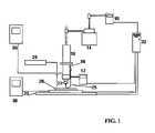
- FIG. 1is schematic of the M 3 DTM apparatus.
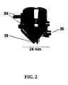
- FIG. 2is a side view of the M 3 DTM flowhead.
- FIG. 3 ais a drawing showing flow-control of a single stage virtual impactor.
- FIG. 3 bis a drawing showing flow-control of a multi-stage virtual impactor.
- FIG. 4shows a silver redistribution circuit deposited on KaptonTM, with lines that are approximately 35 microns wide.
- FIG. 5shows a laser decomposed RF filter circuit on barium titanate, in which VMTool is used to pattern and decompose a silver film deposited on a barium titanate substrate.
- FIG. 6is a schematic representation of a three-layer direct write inductor.
- the present inventionrelates to apparatuses and methods for high-resolution, maskless deposition of liquid and particle suspensions using aerodynamic focusing.
- An aerosol streamis focused and deposited onto any planar or non-planar substrate, forming a pattern that is thermally or photochemically processed to achieve physical and/or electrical properties near that of the corresponding bulk material.
- the processis termed M 3 DTM, Maskless Mesoscale Material Deposition, and is used to deposit aerosolized materials with linewidths that are an order of magnitude smaller than lines deposited with conventional thick film processes. Deposition is performed without the use of masks.
- the term mesoscalerefers to sizes from approximately 10 microns to 1 millimeter, and covers the range between geometries deposited with conventional thin film and thick film processes.
- the M 3 DTM processis capable of defining lines as small as 1 micron in width.
- the present inventioncomprises an apparatus comprising preferably an atomizer for atomizing liquid and particle suspensions, directing, preferably a lower module for directing and focusing the resulting aerosol stream, a control module for automated control of process parameters, a laser delivery module that delivers laser light through an optical fiber, and a motion control module that drives a set of X-Y translation stages.
- the apparatusis functional using only the lower module.
- the laser moduleadds the additional capability of curing materials on low temperature substrates. Aerosolization is accomplished by a number of methods, including using an ultrasonic transducer or a pneumatic nebulizer.
- the aerosol streamis focused using the M 3 DTM flowhead, which forms an annular, co-axial flow between the aerosol stream and a sheath gas stream.
- the M 3 DTM flowheadis capable of focusing an aerosol stream to as small as one-tenth the size of the nozzle orifice. Patterning is accomplished by attaching the substrate to a computer-controlled platen. Alternatively, in a second configuration, the flowhead is translated under computer control while the substrate position remains fixed.
- the aerosolized fluid used in the M 3 DTM processconsists of any liquid source material including, but not limited to, liquid molecular precursors for a particular material, particulate suspensions, or some combination of precursor and particulates.
- the DWBTM processis an extension of the M 3 DTM process wherein biological materials are deposited in mesoscale patterns on a variety of biocompatible substrates. Like the M 3 DTM process, an aerosol is first generated, and materials are deposited onto the desired substrate surface. Stock solutions containing biological molecules such as functional catalytic peptides, extracellular matrix (ECM) and fluorescent proteins, enzymes, or oligonucleotides have all demonstrated post-process functionality. A wide range of biological materials have been deposited using the direct-write method. Indeed, biomaterial aerosols containing biologically active molecules can be deposited into patterned structures to generate engineered substrates. In addition, possible whole cell deposition applications include embedded architecture tissue constructs and tissue-based biosensor development.
- ECMextracellular matrix
- Applications of the M 3 DTM processinclude, but are not limited to, direct write of circuits and devices for electronic applications, as well as the direct write of materials for biological applications.
- FIG. 1shows the preferred M 3 DTM apparatus.
- the M 3 DTM processbegins with the aerosolization of a solution of a liquid molecular precursor or suspension of particles.
- the solutionmay also be a combination of a liquid molecular precursor and particles.
- precursor solutionsmay be atomized using an ultrasonic transducer or pneumatic nebulizer 14 , however ultrasonic aerosolization is limited to solutions with viscosities of approximately 1–10 cP.
- the fluid properties and the final material and electrical properties of the depositare dependent on the precursor chemistry.
- Aerosolization of most particle suspensionsis performed using pneumatics, however ultrasonic aerosolization may be used for particle suspensions consisting of either small or low-density particles.
- the solid particlesmay be suspended in water or an organic solvent and additives that maintain the suspension.
- Fluids with viscosities from approximately 1 to 1000 cPmay be atomized pneumatically.
- the mist produced in the aerosolization processis delivered to a deposition flowhead 22 using a carrier gas.
- the carrier gasis most commonly compressed air or an inert gas, where one or both may contain a modified solvent vapor content.
- the carrier gas flowrateis controlled by a carrier gas controller 10 .
- the aerosolmay be modified while transiting through a heating assembly 18 .
- the heating assembly 18is used to evaporate the precursor solvent and additives or the particle-suspending medium. This evaporation allows for the modification of the fluid properties of the aerosol for optimum deposition. Partial evaporation of the solvent increases the viscosity of the deposited fluid. This increased viscosity allows for greater control of the lateral spreading of the deposit as it contacts the substrate 28 .
- a preheat temperature control 20is used to change the heating assembly's temperature.
- humidifying the carrier gasis necessary to prevent drying of the aerosol stream.
- Humidification of the sheath airflowis accomplished by introducing aerosolized water droplets, vapor, or other non-water based material into the flow. This method is used in the case where the solvent used for a particular precursor material would otherwise completely evaporate before the aerosol reaches the substrate 28 .
- FIG. 2shows the preferred M 3 DTM flowhead.
- the aerosol streamenters through ports mounted on the flowhead 22 and is directed towards the orifice 38 .
- the mass throughputis controlled by the aerosol carrier gas flowrate.
- the aerosol streamis initially collimated by passing through a millimeter-size orifice.
- the emergent particle streamis then combined with an annular sheath gas.
- the sheath gasis most commonly compressed air or an inert gas, where one or both may contain a modified solvent vapor content.
- the sheath gasenters through the sheath air inlet 36 below the aerosol inlet 34 and forms a co-axial flow with the aerosol stream.
- the sheath gasis controlled by a sheath gas controller 12 .
- the combined streamsexit the chamber through an orifice 38 directed at the substrate 28 .
- This co-axial flowfocuses the aerosol stream onto the substrate 28 and allows for deposition of features with dimensions as small as 10 microns.
- the purpose of the sheath gasis to form a boundary layer that both focuses the particle stream and prevents particles from depositing onto the orifice wall. This shielding effect minimizes clogging of the orifices.
- the diameter of the emerging stream(and therefore the linewidth of the deposit) is controlled by the orifice size, the ratio of sheath gas flow rate to carrier gas flow rate, and the spacing between the orifice and the substrate.
- the substrate 28is attached to a platen that moves in two orthogonal directions under computer control via X-Y linear stages 26 , so that intricate geometries may be deposited.
- Another configurationallows for the deposition flowhead to move in two orthogonal directions while maintaining the substrate in a fixed position.
- the processalso allows for the deposition of three-dimensional structures.
- FIG. 3 ashows a single stage virtual impactor.
- a single stage virtual impactorcomprises a nozzle 40 , a large chamber 42 with an exhaust port 44 and a collection probe 46 .
- the nozzle 40 and collection probe 46are opposed to each other within the chamber 42 .
- a particulate laden gas streamreferred to as the total flow, Q 0 is accelerated through the nozzle 40 into the chamber 42 .
- the jet of particulate laden gaspenetrates the collection probe 46 , however most of the gas flow reverses direction and exits the collection probe 46 back into the chamber 42 .
- This flowis referred to as the major flow and is exhausted.
- the flow that remains in the collection probe 46is referred to as the minor flow and is directed downstream for further processing. Particles having sufficient momentum will continue to follow a forward trajectory through the collection probe 46 and will be carried by the minor flow.
- the exhaust gasIn order for the virtual impactor to function properly, the exhaust gas must be removed from the chamber 42 at a specific flowrate. This may be accomplished by feeding the exhaust gas through a flow control device such as a mass flow controller. In the event that ambient conditions do not provide a sufficient pressure drop to achieve the flowrates required for proper operation, a vacuum pump may be used.
- the particles entrained in the gas streamconsist of droplets, generally in the size range of 1–5 microns although droplets smaller than 1 micron and as large as 50 microns may be used. Particles larger than the cut-point enter the collection probe 46 and remain in the process. These are directed into other devices downstream of the impactor. Droplets smaller than the cut-point remain in the stripped excess gas and are no longer part of the process. These may be exhausted to the atmosphere through the exhaust port 44 , filtered to avoid damaging flow control devices, or collected for reuse.
- the efficiency of the virtual impactoris determined by the amount of aerosol that remains in the minor flow and is not stripped out in the major flow along with excess gas or physically impacted out in the virtual impactor. Close geometrical control of the impactor can improve the efficiency, as can control of the particle size distribution in the aerosol. By shifting the particle size distribution above the cut-point of the impactor, all the particles will remain in process, minimizing both waste and clogging. Another option exists to intentionally design an impactor stage to strip off particles below a certain size range, such that only particles above a certain size are presented to the downstream processes. Since the deposition is a physical impaction process, it may be advantageous to present only droplets of a certain size to the substrate. For example, resolution may be improved by depositing only 5 micron sized droplets. Other examples where it may be advantageous to deposit only certain sized droplets include via filling.
- FIG. 3 bshows a multi-stage virtual impactor.
- the output from the collection probe 46 of the first virtual impactoris directed into the nozzle 40 of the second impactor and so on, for the required number of stages.
- a computer-controlled material shutter 25is placed between the flowhead orifice and the substrate 28 .
- FIG. 1shows the shutter.
- the shutter 25functions to interrupt the flow of material to the substrate 28 so that patterning is accomplished.
- a substrate temperature control 30is used to change the temperature of the substrate 28 , as shown in FIG. 1 .
- the M 3 DTM control moduleprovides automated control of process parameters and process monitoring.
- the process parametersinclude the aerosol and sheath gas flowrates, the aerosol preheat temperature and the substrate temperature.
- the control modulemay be operated as a stand-alone unit via manual input on the front panel, or remotely via communication with a host computer. Remote operation via a host computer is preferable for coordinating the deposition system with the other components of the M 3 DTM system.
- the M 3 DTM apparatususes a commercially available laser 24 .
- Depositsare typically processed using a continuous wavelength frequency-doubled Nd:YAG laser, however processing may be accomplished with a variety of lasers, granted that the deposit is absorbing at the laser wavelength.
- the laser delivery modulecomprising a laser, a mechanical shutter, an acousto-optic modulator, delivery optics, and a focusing head.
- the mechanical shutteris used to rapidly turn the laser on and off in coordination with the motion control system.
- the acousto-optic modulatoris used for rapid dynamic power control, which optionally may also be coordinated with motion.
- the delivery opticsmay be either an optical fiber and associated launch optics or mirrors.
- the laser delivery moduleis controlled via communication with the host computer.
- the motion control moduleconsists of a motion control card, an I/O interface, X-Y linear stages 26 for moving either the substrate or the deposition system, a z-axis for positioning the deposition system above the substrate and amplifiers for driving the stages.
- the I/O interface, amplifiers and associated power suppliesare housed in an external, rack mountable enclosure.
- the motion control cardtypically is installed in the host computer and is connected to the I/O interface via a special cable.
- the I/O interfaceconsists of analog outputs to the drive amplifiers and discrete outputs for actuating the material and laser shutters. Control of these components is handled by the motion control module rather than their respective control modules so that the timing of shuttering events can be coordinated with motion.
- the M 3 DTM processhas been used to deposit a range of materials, including electronic and biological materials. Aerosolization of these materials may be from liquid precursor inks, particulate suspensions or combinations of both precursors and particulates. Aerosolization of fluids from roughly 1 to 1000 cP is possible. Biological materials may be deposited without loss of functionality.
- the materials developed specifically for the M 3 DTM processhave low processing temperatures (150° C. to 200° C.), may be written with linewidths as small as 10 microns, have excellent adhesion to plastic, ceramic, and glass substrates, and have electrical properties near that of the bulk material. Electronic materials may be processed thermally, or using laser treatment.
- the M 3 DTM processcan also be used in multiple material deposition.
- the M 3 DTM processcan be used to deposit different materials within a single layer, or it can be used to deposit different materials onto different layers.
- the M 3 DTM processcan be used to deposit metals such as silver, platinum, palladium, rhodium, copper, gold, and silver/palladium and platinum/rhodium alloys.
- metal structuresare formed from aerosolized liquid precursors for the desired metals, however precursors are also formulated with nanometer-size metal particles.
- nanometer-sized metal particlesis beneficial to many aspects of the system, including, but not limited to, optimization of fluid properties, improved densification and final properties of the deposit.
- a particular strength of the apparatus/material combinationis that maskless deposition onto substrates with damage thresholds as low as 150° C. may be achieved. Optimized fluid properties and apparatus parameters also allow for deposition with linewidths as small as 10 microns.
- Subsequent laser processingmay be used to define features with linewidths as small as 1 micron.
- the precursor formulationsalso provide good adhesion to KaptonTM (as shown in FIG. 4 ), glass, barium titanate (as shown in FIG. 5 ), and various plastics.
- the M 3 DTM processcan be used to direct write metal traces with linewidths as small as 1 micron, and as large as 100 microns. Electrical interconnects have been written with linewidths from 10 microns to 250 microns. In general, the resistivity of the traces is from 2 to 5 times that of the bulk metal insulators.
- a silver/glass formulationhas been used as a low-ohmic resistive system, capable of producing traces with resistances from approximately 1 ohm to 1 kohm.
- the formulationconsists of a silver/palladium precursor and a suspension of fumed silica particles.
- the processcan be used to write resistor terminations, interdigitated capacitors, inductive coils, and spiral antennas and patch antennas.
- the M 3 DTM processcan also be used to deposit reflective metals with very low surface roughness for micro-mirror applications.
- the M 3 DTM processcan be used to direct write ceramics, including insulators, mid- and high-k dielectrics, resistor materials and ferrites.
- Source materialshave been precursors, colloidal suspensions and mixtures of the two.
- Low-k dielectric materialssuch as glass have been deposited both for dielectric layers in capacitor applications, as well as insulation or passivation layers.
- High-k dielectricssuch as barium titanate can be deposited for capacitor applications, ruthenates have been deposited to form resistors and manganeses zinc ferrites have been deposited to form inductor cores.
- a broad range of ceramicsmay be deposited and fired conventionally. However, densification on low temperature substrates can only be achieved for materials that can be densified either at temperatures below the damage threshold of the substrate or by laser treatment.
- the M 3 DTM processcan be used to directly write polymeric materials.
- the liquid source materialscan be monomers, solutions, suspensions, or any combination of these.
- Examples of polymers that have been depositedinclude polyimide, polyurethane and UV curable epoxies.
- the final treatment of the depositis dependant on the specific polymer, but may include thermal heating, laser processing or exposure to UV.
- Polymeric depositshave been used as low-k dielectrics for capacitors and overcoat dielectrics for electrical and environmental insulation.
- the M 3 DTM processcan also be used to deposit traditional electronic materials onto polymers, such as polyimide, polyetheretherketone (PEEK), TeflonTM, and polyester, at temperatures below those required to cause damage.
- polymerssuch as polyimide, polyetheretherketone (PEEK), TeflonTM, and polyester, at temperatures below those required to cause damage.
- Resistive traces with resistances spanning six orders of magnitudecan be deposited using the M 3 DTM process.
- a silver/glass formulationhas been used as a low-ohmic system, capable of producing traces with resistances from approximately 1 ohm to 1 kohm.
- the formulationconsists of a silver/palladium precursor and a suspension of fumed silica particles.
- a mid to high ohmic formulationhas been developed using a suspension of ruthenium oxide particles in dimethylacetimide. Resistances from roughly 50 ohm to 1 Mohm are possible with the Ruthenium Oxide system.
- Inductive materialsmay also be deposited using the M 3 DTM process.
- a zinc/manganese ferrite powder combined with a low-melting temperature glass powderhas been atomized and deposited onto KaptonTM. Both thermal and laser processes can be used to sinter the powder. Both processes resulted in a dense well-adhered ferrite layer.
- the M 3 DTM processcan deposit a myriad of other materials for various processes.
- the M 3 DTM processcan be used to deposit sacrificial and resist materials for subsequent processing of a substrate, such as in chemical etching. It can also deposit sacrificial materials to form support structures onto or into a structure using additional materials.
- the M 3 DTM processcan deposit solvent and etching chemicals to directly texture a substrate.
- the M 3 DTM processcan also be used to deposit dissimilar materials in the same location for further processing to form a multi-phase mixture, alloy, or compound, and it can deposit dissimilar materials to form structures with a compositional gradient.
- the M 3 DTM processcan create porosity or channels in structures by depositing fugitive materials for later removal.
- the M 3 DTM processcan also deposit materials, which are structural in nature.
- thermal treatmentor laser treatment may be used to process deposited materials to the desired state.
- dense metal linesmay be formed with thermal decomposition temperatures as low as 150° C.
- thermal treatmentis used to raise the temperature of the deposit to its decomposition or curing temperature.
- a chemical decomposition or crosslinkingtakes place as a result of the input of thermal energy, such that the precursor changes its molecular state, resulting in the desired material plus some effluents.
- An example of a chemical decomposition of a molecular precursor to a metalis that of the reaction of silver nitrate, a metal salt, to form silver plus nitrogen, oxygen, and nitrogen/oxygen compounds.
- the precursor or precursor/particle combinationis formulated so that the fluid is absorbing at the laser wavelength.
- the high absorption coefficient at the laser wavelengthallows for very localized heating of the deposit, which in turn may be used to produce fine deposits (as small as 1 micron for a frequency-doubled Nd: YAG laser) with no damage to the substrate.
- the M 3 DTM processhas been used to deposit and laser process silver on an FR4 substrate, which has a damage threshold of less than 200° C.
- laser sinteringis used to soften low-melting temperature particles used to bind the refractory powder.
- the laseris scanned over the deposit and absorbed by the glass or the powder, softening the glass to the point that adhesion takes place between particles and the substrate.
- thermal treatmentis used to incubate deposited samples.
- the goal of incubationis to produce a desired chemical reaction, such as the development of enzyme activity.
- Cell patterning by flow-guided direct writingmay revolutionize cell patterning technology by allowing for precise cellular micro-patterning and addition of biologically active adhesion or pathway signaling biomolecules. This is the most general advantage and arguably the most revolutionary component of the DWBTM technology.
- the direct-write methodcan be used to guide and deposit 0.02 ⁇ m to 20 ⁇ m diameter biological particles onto substrate surfaces.
- the range of biological materials that can be depositedis extremely broad, and includes polymers, peptides, viruses, proteinaceous enzymes and ECM biomolecules, as well as whole bacterial, yeast, and mammalian cell suspensions.
- the first deviceis a manganese-zinc ferrite inductor written on alumina, as shown in FIG. 6 .
- This devicedemonstrates deposition of silver precursor plus laser processing of the deposit.
- the silver precursoris ultrasonically atomized from liquid precursor solution,
- a ferrite and glass particle suspensionis pneumatically atomized, deposited, and laser densified.
- the silver depositionillustrates the capability to deposit over a non-planar surface.
- the second deviceis a silver spiral on KaptonTM, demonstrating fine feature size and direct write of silver onto a low-temperature substrate.
- FIG. 6shows a three-layer direct write inductor.
- the first step of the inductor fabricationis the deposition of parallel lines of silver precursor 56 onto an alumina substrate.
- the linesare approximately 100 microns wide, 1 micron thick and 1000 microns in length.
- the linesare laser treated to form dense, conductive silver wires. These wires are one-half of the conductive traces that will eventually wrap around a ferrite core.
- Silver contact pads 58 a–b(1000 micron square) are also added in the first layer.
- the second stepis to create the inductor core 60 by depositing a mixture of Manganese-Zinc Ferrite powder and low melting temperature glass over the conductive lines. Laser sintering is used to densify the ferrite/glass deposit; the glass flows around the ferrite particles and forms a dense, connected solid after cooling.
- the ferrite deposition stepis repeated several times to buildup the deposit to about 150 microns.
- the ferrite line lengthsare about 1500 mm long.
- a typical profile of the ferrite layeris shown in FIG. 6 .
- the final stepis to write conductive traces over the ferrite layer and connect them to the underlying traces to form the inductor coil 62 . Since the flowguide head standoff distance is several mm, deposition over a mm-sized non-planar surface is possible. The resistance of a typical coil generated using this method is on the order of several ohms. The inductance is 7 micro henries and the Q value is 4.2 @ 1 MHz.
- the M 3 DTM processhas been used to form a direct write spiral, which shows the line definition and feature size capabilities of the process.
- the spiral linesare 35 microns in diameter on a 60-micron pitch.
- the overall diameter of the coilis 2.0 mm.
- the start materialis silver ink that was deposited and then treated at 200° C. to chemically decompose the precursors and densify the deposit. In depositing this pattern, the substrate was translated beneath the deposition head at a speed of 10 mm/s.
- the M 3 DTM processcan be used to perform a plethora of other applications. It can perform layerwise deposition of materials to form functional devices, such as multilayer capacitors, sensors, and terminated resistors. It has the capacity to deposit multiple materials to form structures, such as interconnects, resistors, inductors, capacitors, thermocouples, and heaters, on a single layer.
- the M 3 DTM processcan deposit multilayer structures consisting of conductor patterns and dielectric insulating layers, in which the conductor patterns may be electrically connected by conducting vias. It can deposit a passivation material to protect or insulate electronic structures. It can deposit overlay deposits for the purpose of “additive trimming” of a circuit element, such as adding material to a resistor to alter its value.
- the M 3 DTM processcan also deposit these overlay deposits on top of existing structures, which is difficult to achieve with screen printing.
- the M 3 DTM processcan deposit materials between preexisting features to alter a circuit or repair broken segments. It can deposit metal films with tapered linewidths for devices, such as a stripline antennae. It can also deposit material to form “bumps” for chip attachment.
- the M 3 DTM processcan deposit adhesive materials to form dots or lines for application to bonding multiple substrates and devices.
- the M 3 DTM processcan also deposit materials into underfill regions, in which the deposit is pulled into the underfill region by capillary forces.
- the M 3 DTM processcan deposit three-dimensional patterns to fabricate a master stamp. It can also deposit colored pigments (e.g. red, green, blue) to generate high resolution colored deposits.
- colored pigmentse.g. red, green, blue
- the M 3 DTM processmay also be used in several optoelectronic applications, and can deposit transparent polymers into lines and dots to serve as lenses and optical conductors. It can also deposit repetitive structures, such as lines and dots, to refract or reflect light and to serve as diffractive optical elements, such as diffraction gratings or photonic bandgaps. It can deposit metal and dielectric films with tapered film thickness, in which the films can serve as optical phase retarders that can encode holographic information into light beams. Examples of this are phase shift masks, diffractive optical elements, and holograms.
- the M 3 DTM processcan also deposit metal and opaque films of variable thickness for controlled reflection and absorption of light. Such a process can be used to make high-resolution portraits.
- the M 3 DTM processcan deposit materials that form a thermal or chemical barrier to the underlying substrate. It can deposit materials that have a primary function of bearing a load, reducing friction between moving parts, or increasing friction between moving parts. It can also deposit materials used to form memory devices. Further, the M 3 DTM process can deposit materials that form a logic gate.
- the DWBTM initiativemay be applied to material deposition applications including biosensor rapid prototyping and microfabrication, microarray bio-chip manufacturing, bioinspired electroactive polymer concept development (ambient temperature bio-production of electronic circuitry), and various additive biomaterial processes for hybrid BioMEMS and Bio-Optics. Moreover, the ability to deposit electronic and biologically viable or active materials with mesoscale accuracy has potential to advance these application areas.
- the M 3 DTM processcan also be used to deposit multiple materials in a dot-array geometry for biological applications, such as for protein and DNA arrays. It can deposit passivation material to protect or insulate biological structures. It can also deposit an overlay material onto an existing structure that selectively allows migration of certain chemical or biological species to the existing structure while preventing the passage of others. Further, the M 3 DTM process can deposit materials containing a chemical or biological species that is released as a function of time or an internal or external stimulus.
- the M 3 DTM processcan perform various topological depositions. For example, it can deposit spots, lines, filled areas, or three-dimensional shapes. It has the capability to perform conformal deposition over curved surfaces and steps. It can deposit into channels or trenches, or onto the sides of channel walls. It can deposit into via holes as small as 25 microns.
- the M 3 DTM processcan deposit across multiple substrate materials. It can deposit longitudinally or circumferentially around cylinderically-shaped objects. It can also deposit both internally or externally onto geometrical shapes having flat faces that meet as sharp corners, such as cubes.
- the M 3 DTM processcan deposit onto previously deposited material. It can also deposit films with variable layer thickness. Further, the M 3 DTM process can deposit films or lines with variable widths.
Landscapes
- Chemical & Material Sciences (AREA)
- Engineering & Computer Science (AREA)
- Metallurgy (AREA)
- Organic Chemistry (AREA)
- Chemical Kinetics & Catalysis (AREA)
- General Chemical & Material Sciences (AREA)
- Materials Engineering (AREA)
- Mechanical Engineering (AREA)
- Physics & Mathematics (AREA)
- Health & Medical Sciences (AREA)
- Toxicology (AREA)
- Thermal Sciences (AREA)
- Manufacturing & Machinery (AREA)
- Microelectronics & Electronic Packaging (AREA)
- Plasma & Fusion (AREA)
- Other Surface Treatments For Metallic Materials (AREA)
- Physical Or Chemical Processes And Apparatus (AREA)
Abstract
Description
FIG. 1 - 10 Carrier gas controller
- 12 Sheath gas controller
- 14 Pneumatic nebulizer/Ultrasonic atomizer
- 16 Virtual impactor
- 18 Heating assembly
- 20 Preheat temperature control
- 22 Flowhead
- 24 Processing laser
- 25 Shutter
- 26 X-Y linear stages
- 28 Substrate
- 30 Substrate temperature control
- 32 Computer
FIG. 2 - 34 Aerosol/carrier gas inlet
- 36 Sheath air inlet
- 38 Orifice
FIG. 3 a- 40 Nozzle
- 42 Chamber
- 44 Exhaust port
- 46 Collection probe
FIG. 3 b- No new reference numerals required.
FIG. 4 - No reference numerals required.
FIG. 5 - No reference numerals required.
FIG. 6 - 56 Parallel lines of
silver precursor 58a–bSilver contact pads - 60 Inductor core
- 62 Inductor coil
Claims (3)
Priority Applications (9)
| Application Number | Priority Date | Filing Date | Title |
|---|---|---|---|
| US10/346,935US7045015B2 (en) | 1998-09-30 | 2003-01-17 | Apparatuses and method for maskless mesoscale material deposition |
| US10/746,646US20040197493A1 (en) | 1998-09-30 | 2003-12-23 | Apparatus, methods and precision spray processes for direct write and maskless mesoscale material deposition |
| US10/952,108US7294366B2 (en) | 1998-09-30 | 2004-09-27 | Laser processing for heat-sensitive mesoscale deposition |
| US11/011,366US7938079B2 (en) | 1998-09-30 | 2004-12-13 | Annular aerosol jet deposition using an extended nozzle |
| US11/317,457US7485345B2 (en) | 1998-09-30 | 2005-12-22 | Apparatuses and methods for maskless mesoscale material deposition |
| US11/430,636US8110247B2 (en) | 1998-09-30 | 2006-05-08 | Laser processing for heat-sensitive mesoscale deposition of oxygen-sensitive materials |
| US12/349,279US7987813B2 (en) | 1998-09-30 | 2009-01-06 | Apparatuses and methods for maskless mesoscale material deposition |
| US12/976,906US8455051B2 (en) | 1998-09-30 | 2010-12-22 | Apparatuses and methods for maskless mesoscale material deposition |
| US13/909,870US20130260056A1 (en) | 1998-09-30 | 2013-06-04 | Apparatuses and Methods for Maskless Mesoscale Material Deposition |
Applications Claiming Priority (7)
| Application Number | Priority Date | Filing Date | Title |
|---|---|---|---|
| US10241898P | 1998-09-30 | 1998-09-30 | |
| US40862199A | 1999-09-30 | 1999-09-30 | |
| US09/574,955US6823124B1 (en) | 1998-09-30 | 2000-05-19 | Laser-guided manipulation of non-atomic particles |
| US09/584,997US6636676B1 (en) | 1998-09-30 | 2000-06-01 | Particle guidance system |
| US10/060,960US20030020768A1 (en) | 1998-09-30 | 2002-01-30 | Direct write TM system |
| US10/072,605US7108894B2 (en) | 1998-09-30 | 2002-02-05 | Direct Write™ System |
| US10/346,935US7045015B2 (en) | 1998-09-30 | 2003-01-17 | Apparatuses and method for maskless mesoscale material deposition |
Related Parent Applications (5)
| Application Number | Title | Priority Date | Filing Date |
|---|---|---|---|
| US40862199AContinuation | 1998-09-30 | 1999-09-30 | |
| US09/574,955Continuation-In-PartUS6823124B1 (en) | 1998-09-30 | 2000-05-19 | Laser-guided manipulation of non-atomic particles |
| US09/584,997Continuation-In-PartUS6636676B1 (en) | 1998-09-30 | 2000-06-01 | Particle guidance system |
| US10/060,960Continuation-In-PartUS20030020768A1 (en) | 1998-09-30 | 2002-01-30 | Direct write TM system |
| US10/072,605Continuation-In-PartUS7108894B2 (en) | 1998-09-30 | 2002-02-05 | Direct Write™ System |
Related Child Applications (2)
| Application Number | Title | Priority Date | Filing Date |
|---|---|---|---|
| US10/746,646Continuation-In-PartUS20040197493A1 (en) | 1998-09-30 | 2003-12-23 | Apparatus, methods and precision spray processes for direct write and maskless mesoscale material deposition |
| US11/317,457DivisionUS7485345B2 (en) | 1998-09-30 | 2005-12-22 | Apparatuses and methods for maskless mesoscale material deposition |
Publications (2)
| Publication Number | Publication Date |
|---|---|
| US20030228124A1 US20030228124A1 (en) | 2003-12-11 |
| US7045015B2true US7045015B2 (en) | 2006-05-16 |
Family
ID=29716390
Family Applications (5)
| Application Number | Title | Priority Date | Filing Date |
|---|---|---|---|
| US10/346,935Expired - LifetimeUS7045015B2 (en) | 1998-09-30 | 2003-01-17 | Apparatuses and method for maskless mesoscale material deposition |
| US11/317,457Expired - Fee RelatedUS7485345B2 (en) | 1998-09-30 | 2005-12-22 | Apparatuses and methods for maskless mesoscale material deposition |
| US12/349,279Expired - Fee RelatedUS7987813B2 (en) | 1998-09-30 | 2009-01-06 | Apparatuses and methods for maskless mesoscale material deposition |
| US12/976,906Expired - Fee RelatedUS8455051B2 (en) | 1998-09-30 | 2010-12-22 | Apparatuses and methods for maskless mesoscale material deposition |
| US13/909,870AbandonedUS20130260056A1 (en) | 1998-09-30 | 2013-06-04 | Apparatuses and Methods for Maskless Mesoscale Material Deposition |
Family Applications After (4)
| Application Number | Title | Priority Date | Filing Date |
|---|---|---|---|
| US11/317,457Expired - Fee RelatedUS7485345B2 (en) | 1998-09-30 | 2005-12-22 | Apparatuses and methods for maskless mesoscale material deposition |
| US12/349,279Expired - Fee RelatedUS7987813B2 (en) | 1998-09-30 | 2009-01-06 | Apparatuses and methods for maskless mesoscale material deposition |
| US12/976,906Expired - Fee RelatedUS8455051B2 (en) | 1998-09-30 | 2010-12-22 | Apparatuses and methods for maskless mesoscale material deposition |
| US13/909,870AbandonedUS20130260056A1 (en) | 1998-09-30 | 2013-06-04 | Apparatuses and Methods for Maskless Mesoscale Material Deposition |
Country Status (1)
| Country | Link |
|---|---|
| US (5) | US7045015B2 (en) |
Cited By (113)
| Publication number | Priority date | Publication date | Assignee | Title |
|---|---|---|---|---|
| US20030161959A1 (en)* | 2001-11-02 | 2003-08-28 | Kodas Toivo T. | Precursor compositions for the deposition of passive electronic features |
| US20030180451A1 (en)* | 2001-10-05 | 2003-09-25 | Kodas Toivo T. | Low viscosity copper precursor compositions and methods for the deposition of conductive electronic features |
| US20050127478A1 (en)* | 2003-12-10 | 2005-06-16 | Hiatt William M. | Microelectronic devices and methods for filling vias in microelectronic devices |
| US20050156991A1 (en)* | 1998-09-30 | 2005-07-21 | Optomec Design Company | Maskless direct write of copper using an annular aerosol jet |
| US20050287783A1 (en)* | 2004-06-29 | 2005-12-29 | Kirby Kyle K | Microelectronic devices and methods for forming interconnects in microelectronic devices |
| US20060043534A1 (en)* | 2004-08-26 | 2006-03-02 | Kirby Kyle K | Microfeature dies with porous regions, and associated methods and systems |
| US20060175431A1 (en)* | 2004-12-13 | 2006-08-10 | Optomec Design Company | Miniature aerosol jet and aerosol jet array |
| US20060177999A1 (en)* | 2005-02-10 | 2006-08-10 | Micron Technology, Inc. | Microelectronic workpieces and methods for forming interconnects in microelectronic workpieces |
| US20070019028A1 (en)* | 1998-09-30 | 2007-01-25 | Optomec Design Company | Laser processing for heat-sensitive mesoscale deposition of oxygen-sensitive materials |
| US7228053B1 (en)* | 2004-06-21 | 2007-06-05 | Yoram Palti | Transporting matter that is enclosed within a container through a hollow optical fiber |
| US20070181060A1 (en)* | 1998-09-30 | 2007-08-09 | Optomec Design Company | Direct Write™ System |
| US20080050911A1 (en)* | 2006-08-28 | 2008-02-28 | Micron Technology, Inc. | Microfeature workpieces having conductive interconnect structures formed by chemically reactive processes, and associated systems and methods |
| US20080081007A1 (en)* | 2006-09-29 | 2008-04-03 | Mott Corporation, A Corporation Of The State Of Connecticut | Sinter bonded porous metallic coatings |
| US20080174040A1 (en)* | 2006-11-08 | 2008-07-24 | John Charles Saukaitis | Gas separation membrane system and method of making thereof using nanoscale metal material |
| US7413979B2 (en) | 2003-11-13 | 2008-08-19 | Micron Technology, Inc. | Methods for forming vias in microelectronic devices, and methods for packaging microelectronic devices |
| US7425499B2 (en) | 2004-08-24 | 2008-09-16 | Micron Technology, Inc. | Methods for forming interconnects in vias and microelectronic workpieces including such interconnects |
| US7435913B2 (en) | 2004-08-27 | 2008-10-14 | Micron Technology, Inc. | Slanted vias for electrical circuits on circuit boards and other substrates |
| US20080282882A1 (en)* | 2006-11-08 | 2008-11-20 | John Charles Saukaitis | gas separation membrane comprising a substrate with a layer of coated inorganic oxide particles and an overlayer of a gas-selective material, and its manufacture and use |
| US20080314214A1 (en)* | 2000-06-13 | 2008-12-25 | Klaus Tank | Composite diamond compacts |
| US20090053507A1 (en)* | 2007-08-17 | 2009-02-26 | Ndsu Research Foundation | Convergent-divergent-convergent nozzle focusing of aerosol particles for micron-scale direct writing |
| US20090061089A1 (en)* | 2007-08-30 | 2009-03-05 | Optomec, Inc. | Mechanically Integrated and Closely Coupled Print Head and Mist Source |
| US20090061077A1 (en)* | 2007-08-31 | 2009-03-05 | Optomec, Inc. | Aerosol Jet (R) printing system for photovoltaic applications |
| US20090090298A1 (en)* | 2007-08-31 | 2009-04-09 | Optomec, Inc. | Apparatus for Anisotropic Focusing |
| US20090114151A1 (en)* | 1998-09-30 | 2009-05-07 | Optomec, Inc. Fka Optomec Design Company | Apparatuses and Methods for Maskless Mesoscale Material Deposition |
| US7589008B2 (en) | 2004-12-30 | 2009-09-15 | Micron Technology, Inc. | Methods for forming interconnects in microelectronic workpieces and microelectronic workpieces formed using such methods |
| US20090252874A1 (en)* | 2007-10-09 | 2009-10-08 | Optomec, Inc. | Multiple Sheath Multiple Capillary Aerosol Jet |
| US20090269481A1 (en)* | 2008-04-24 | 2009-10-29 | Chappa Ralph A | Coating application system with shaped mandrel |
| US7622377B2 (en) | 2005-09-01 | 2009-11-24 | Micron Technology, Inc. | Microfeature workpiece substrates having through-substrate vias, and associated methods of formation |
| US20090312878A1 (en)* | 2008-06-11 | 2009-12-17 | Boston Scientific Scimed, Inc. | Precision Pen Height Control for Micro-Scale Direct Writing Technology |
| US7674671B2 (en) | 2004-12-13 | 2010-03-09 | Optomec Design Company | Aerodynamic jetting of aerosolized fluids for fabrication of passive structures |
| US7683458B2 (en) | 2004-09-02 | 2010-03-23 | Micron Technology, Inc. | Through-wafer interconnects for photoimager and memory wafers |
| US20100112195A1 (en)* | 2001-10-19 | 2010-05-06 | Kodas Toivo T | Method for the fabrication of conductive electronic features |
| US7749899B2 (en) | 2006-06-01 | 2010-07-06 | Micron Technology, Inc. | Microelectronic workpieces and methods and systems for forming interconnects in microelectronic workpieces |
| US20100207291A1 (en)* | 2009-02-13 | 2010-08-19 | Boston Scientific Scimed, Inc. | Method of Making a Tubular Member |
| US7795134B2 (en) | 2005-06-28 | 2010-09-14 | Micron Technology, Inc. | Conductive interconnect structures and formation methods using supercritical fluids |
| US7830018B2 (en) | 2007-08-31 | 2010-11-09 | Micron Technology, Inc. | Partitioned through-layer via and associated systems and methods |
| US20100310630A1 (en)* | 2007-04-27 | 2010-12-09 | Technische Universitat Braunschweig | Coated surface for cell culture |
| US7863187B2 (en) | 2005-09-01 | 2011-01-04 | Micron Technology, Inc. | Microfeature workpieces and methods for forming interconnects in microfeature workpieces |
| US7884015B2 (en) | 2007-12-06 | 2011-02-08 | Micron Technology, Inc. | Methods for forming interconnects in microelectronic workpieces and microelectronic workpieces formed using such methods |
| US7902643B2 (en) | 2006-08-31 | 2011-03-08 | Micron Technology, Inc. | Microfeature workpieces having interconnects and conductive backplanes, and associated systems and methods |
| US7915736B2 (en) | 2005-09-01 | 2011-03-29 | Micron Technology, Inc. | Microfeature workpieces and methods for forming interconnects in microfeature workpieces |
| US20110211246A1 (en)* | 2008-01-31 | 2011-09-01 | Ajjer Llc | Conductive busbars and sealants for chromogenic devices |
| US8525346B2 (en) | 2009-06-02 | 2013-09-03 | Hsio Technologies, Llc | Compliant conductive nano-particle electrical interconnect |
| US8536485B2 (en) | 2004-05-05 | 2013-09-17 | Micron Technology, Inc. | Systems and methods for forming apertures in microfeature workpieces |
| US8610265B2 (en) | 2009-06-02 | 2013-12-17 | Hsio Technologies, Llc | Compliant core peripheral lead semiconductor test socket |
| US8618649B2 (en) | 2009-06-02 | 2013-12-31 | Hsio Technologies, Llc | Compliant printed circuit semiconductor package |
| US8758067B2 (en) | 2010-06-03 | 2014-06-24 | Hsio Technologies, Llc | Selective metalization of electrical connector or socket housing |
| US8789272B2 (en) | 2009-06-02 | 2014-07-29 | Hsio Technologies, Llc | Method of making a compliant printed circuit peripheral lead semiconductor test socket |
| US8803539B2 (en) | 2009-06-03 | 2014-08-12 | Hsio Technologies, Llc | Compliant wafer level probe assembly |
| US8912812B2 (en) | 2009-06-02 | 2014-12-16 | Hsio Technologies, Llc | Compliant printed circuit wafer probe diagnostic tool |
| US8928344B2 (en) | 2009-06-02 | 2015-01-06 | Hsio Technologies, Llc | Compliant printed circuit socket diagnostic tool |
| US8955215B2 (en) | 2009-05-28 | 2015-02-17 | Hsio Technologies, Llc | High performance surface mount electrical interconnect |
| US8955216B2 (en) | 2009-06-02 | 2015-02-17 | Hsio Technologies, Llc | Method of making a compliant printed circuit peripheral lead semiconductor package |
| US8970031B2 (en) | 2009-06-16 | 2015-03-03 | Hsio Technologies, Llc | Semiconductor die terminal |
| US8981809B2 (en) | 2009-06-29 | 2015-03-17 | Hsio Technologies, Llc | Compliant printed circuit semiconductor tester interface |
| US8981568B2 (en) | 2009-06-16 | 2015-03-17 | Hsio Technologies, Llc | Simulated wirebond semiconductor package |
| US8987886B2 (en) | 2009-06-02 | 2015-03-24 | Hsio Technologies, Llc | Copper pillar full metal via electrical circuit structure |
| US8988093B2 (en) | 2009-06-02 | 2015-03-24 | Hsio Technologies, Llc | Bumped semiconductor wafer or die level electrical interconnect |
| US8984748B2 (en) | 2009-06-29 | 2015-03-24 | Hsio Technologies, Llc | Singulated semiconductor device separable electrical interconnect |
| US9054097B2 (en) | 2009-06-02 | 2015-06-09 | Hsio Technologies, Llc | Compliant printed circuit area array semiconductor device package |
| US9093767B2 (en) | 2009-06-02 | 2015-07-28 | Hsio Technologies, Llc | High performance surface mount electrical interconnect |
| US9136196B2 (en) | 2009-06-02 | 2015-09-15 | Hsio Technologies, Llc | Compliant printed circuit wafer level semiconductor package |
| US9149750B2 (en) | 2006-09-29 | 2015-10-06 | Mott Corporation | Sinter bonded porous metallic coatings |
| US9165888B2 (en) | 2008-09-11 | 2015-10-20 | Micron Technology, Inc. | Interconnect structures for stacked dies, including penetrating structures for through-silicon vias, and associated systems and methods |
| US9184145B2 (en) | 2009-06-02 | 2015-11-10 | Hsio Technologies, Llc | Semiconductor device package adapter |
| US9184527B2 (en) | 2009-06-02 | 2015-11-10 | Hsio Technologies, Llc | Electrical connector insulator housing |
| US9196980B2 (en) | 2009-06-02 | 2015-11-24 | Hsio Technologies, Llc | High performance surface mount electrical interconnect with external biased normal force loading |
| US9232654B2 (en) | 2009-06-02 | 2016-01-05 | Hsio Technologies, Llc | High performance electrical circuit structure |
| US9231328B2 (en) | 2009-06-02 | 2016-01-05 | Hsio Technologies, Llc | Resilient conductive electrical interconnect |
| US9254535B2 (en) | 2014-06-20 | 2016-02-09 | Velo3D, Inc. | Apparatuses, systems and methods for three-dimensional printing |
| US9276336B2 (en) | 2009-05-28 | 2016-03-01 | Hsio Technologies, Llc | Metalized pad to electrical contact interface |
| US9277654B2 (en) | 2009-06-02 | 2016-03-01 | Hsio Technologies, Llc | Composite polymer-metal electrical contacts |
| US9276339B2 (en) | 2009-06-02 | 2016-03-01 | Hsio Technologies, Llc | Electrical interconnect IC device socket |
| US9283350B2 (en) | 2012-12-07 | 2016-03-15 | Surmodics, Inc. | Coating apparatus and methods |
| US9308355B2 (en) | 2012-06-01 | 2016-04-12 | Surmodies, Inc. | Apparatus and methods for coating medical devices |
| US9320144B2 (en) | 2009-06-17 | 2016-04-19 | Hsio Technologies, Llc | Method of forming a semiconductor socket |
| US9318862B2 (en) | 2009-06-02 | 2016-04-19 | Hsio Technologies, Llc | Method of making an electronic interconnect |
| US9320133B2 (en) | 2009-06-02 | 2016-04-19 | Hsio Technologies, Llc | Electrical interconnect IC device socket |
| US9350093B2 (en) | 2010-06-03 | 2016-05-24 | Hsio Technologies, Llc | Selective metalization of electrical connector or socket housing |
| US9414500B2 (en) | 2009-06-02 | 2016-08-09 | Hsio Technologies, Llc | Compliant printed flexible circuit |
| US9536815B2 (en) | 2009-05-28 | 2017-01-03 | Hsio Technologies, Llc | Semiconductor socket with direct selective metalization |
| US9559447B2 (en) | 2015-03-18 | 2017-01-31 | Hsio Technologies, Llc | Mechanical contact retention within an electrical connector |
| US9603249B2 (en) | 2009-06-02 | 2017-03-21 | Hsio Technologies, Llc | Direct metalization of electrical circuit structures |
| US9613841B2 (en) | 2009-06-02 | 2017-04-04 | Hsio Technologies, Llc | Area array semiconductor device package interconnect structure with optional package-to-package or flexible circuit to package connection |
| US9662840B1 (en) | 2015-11-06 | 2017-05-30 | Velo3D, Inc. | Adept three-dimensional printing |
| US9689897B2 (en) | 2010-06-03 | 2017-06-27 | Hsio Technologies, Llc | Performance enhanced semiconductor socket |
| US9699906B2 (en) | 2009-06-02 | 2017-07-04 | Hsio Technologies, Llc | Hybrid printed circuit assembly with low density main core and embedded high density circuit regions |
| US9761520B2 (en) | 2012-07-10 | 2017-09-12 | Hsio Technologies, Llc | Method of making an electrical connector having electrodeposited terminals |
| US9827401B2 (en) | 2012-06-01 | 2017-11-28 | Surmodics, Inc. | Apparatus and methods for coating medical devices |
| US9919360B2 (en) | 2016-02-18 | 2018-03-20 | Velo3D, Inc. | Accurate three-dimensional printing |
| US9930775B2 (en) | 2009-06-02 | 2018-03-27 | Hsio Technologies, Llc | Copper pillar full metal via electrical circuit structure |
| US9962767B2 (en) | 2015-12-10 | 2018-05-08 | Velo3D, Inc. | Apparatuses for three-dimensional printing |
| US20180126649A1 (en) | 2016-11-07 | 2018-05-10 | Velo3D, Inc. | Gas flow in three-dimensional printing |
| US10086432B2 (en) | 2014-12-10 | 2018-10-02 | Washington State University | Three dimensional sub-mm wavelength sub-THz frequency antennas on flexible and UV-curable dielectric using printed electronic metal traces |
| US10144176B1 (en) | 2018-01-15 | 2018-12-04 | Velo3D, Inc. | Three-dimensional printing systems and methods of their use |
| US10159154B2 (en) | 2010-06-03 | 2018-12-18 | Hsio Technologies, Llc | Fusion bonded liquid crystal polymer circuit structure |
| US10252336B2 (en) | 2016-06-29 | 2019-04-09 | Velo3D, Inc. | Three-dimensional printing and three-dimensional printers |
| US10272525B1 (en) | 2017-12-27 | 2019-04-30 | Velo3D, Inc. | Three-dimensional printing systems and methods of their use |
| US10315252B2 (en) | 2017-03-02 | 2019-06-11 | Velo3D, Inc. | Three-dimensional printing of three-dimensional objects |
| US10449696B2 (en) | 2017-03-28 | 2019-10-22 | Velo3D, Inc. | Material manipulation in three-dimensional printing |
| US10506722B2 (en) | 2013-07-11 | 2019-12-10 | Hsio Technologies, Llc | Fusion bonded liquid crystal polymer electrical circuit structure |
| US10611092B2 (en) | 2017-01-05 | 2020-04-07 | Velo3D, Inc. | Optics in three-dimensional printing |
| US10632746B2 (en) | 2017-11-13 | 2020-04-28 | Optomec, Inc. | Shuttering of aerosol streams |
| US10667410B2 (en) | 2013-07-11 | 2020-05-26 | Hsio Technologies, Llc | Method of making a fusion bonded circuit structure |
| US10994473B2 (en) | 2015-02-10 | 2021-05-04 | Optomec, Inc. | Fabrication of three dimensional structures by in-flight curing of aerosols |
| US11090468B2 (en) | 2012-10-25 | 2021-08-17 | Surmodics, Inc. | Apparatus and methods for coating medical devices |
| US11628466B2 (en) | 2018-11-29 | 2023-04-18 | Surmodics, Inc. | Apparatus and methods for coating medical devices |
| US11691343B2 (en) | 2016-06-29 | 2023-07-04 | Velo3D, Inc. | Three-dimensional printing and three-dimensional printers |
| US11819590B2 (en) | 2019-05-13 | 2023-11-21 | Surmodics, Inc. | Apparatus and methods for coating medical devices |
| US11999110B2 (en) | 2019-07-26 | 2024-06-04 | Velo3D, Inc. | Quality assurance in formation of three-dimensional objects |
| US12070907B2 (en) | 2016-09-30 | 2024-08-27 | Velo3D | Three-dimensional objects and their formation |
| US12162035B2 (en) | 2021-07-28 | 2024-12-10 | Oregon State University | Print head for printing nanomaterials |
| US12172444B2 (en) | 2021-04-29 | 2024-12-24 | Optomec, Inc. | High reliability sheathed transport path for aerosol jet devices |
Families Citing this family (60)
| Publication number | Priority date | Publication date | Assignee | Title |
|---|---|---|---|---|
| US7938079B2 (en) | 1998-09-30 | 2011-05-10 | Optomec Design Company | Annular aerosol jet deposition using an extended nozzle |
| EP1670610B1 (en) | 2003-09-26 | 2018-05-30 | Optomec Design Company | Laser processing for heat-sensitive mesoscale deposition |
| WO2005078533A1 (en)* | 2004-02-10 | 2005-08-25 | Zebra Imaging, Inc. | Deposition of photosensitive media for digital hologram recording |
| US7334881B2 (en)* | 2004-07-12 | 2008-02-26 | Hewlett-Packard Development Company, L.P. | Method and system to deposit drops |
| US20060280866A1 (en)* | 2004-10-13 | 2006-12-14 | Optomec Design Company | Method and apparatus for mesoscale deposition of biological materials and biomaterials |
| US20070154634A1 (en)* | 2005-12-15 | 2007-07-05 | Optomec Design Company | Method and Apparatus for Low-Temperature Plasma Sintering |
| US20100248975A1 (en)* | 2006-12-29 | 2010-09-30 | Gunjan Tiwari | Fluorogenic peptide substrate arrays for highly multiplexed, real-time monitoring of kinase activities |
| JP2009302136A (en)* | 2008-06-10 | 2009-12-24 | Panasonic Corp | Semiconductor integrated circuit |
| DE102009007800A1 (en)* | 2009-02-06 | 2010-08-12 | Fraunhofer-Gesellschaft zur Förderung der angewandten Forschung e.V. | Aerosol printers, their use and methods of producing line breaks in continuous aerosol printing processes |
| US8801497B2 (en) | 2009-04-30 | 2014-08-12 | Rdc Holdings, Llc | Array of abrasive members with resilient support |
| US20110104989A1 (en)* | 2009-04-30 | 2011-05-05 | First Principles LLC | Dressing bar for embedding abrasive particles into substrates |
| US9221148B2 (en) | 2009-04-30 | 2015-12-29 | Rdc Holdings, Llc | Method and apparatus for processing sliders for disk drives, and to various processing media for the same |
| JP5629767B2 (en) | 2009-06-09 | 2014-11-26 | ヴィデオジェット テクノロジーズ インコーポレイテッド | Flow printing method |
| US20110318503A1 (en)* | 2010-06-29 | 2011-12-29 | Christian Adams | Plasma enhanced materials deposition system |
| US8635767B2 (en) | 2011-01-05 | 2014-01-28 | Thoe Boeing Company | System for depositing microwire |
| EP2574458A1 (en) | 2011-09-30 | 2013-04-03 | Agfa Graphics N.V. | Method of preparing a flexographic printing master |
| US8808373B2 (en) | 2012-06-13 | 2014-08-19 | Elwha Llc | Breast implant with regionalized analyte sensors responsive to external power source |
| US9144489B2 (en) | 2012-06-13 | 2015-09-29 | Elwha Llc | Breast implant with covering, analyte sensors and internal power source |
| US8790400B2 (en) | 2012-06-13 | 2014-07-29 | Elwha Llc | Breast implant with covering and analyte sensors responsive to external power source |
| US8795359B2 (en) | 2012-06-13 | 2014-08-05 | Elwha Llc | Breast implant with regionalized analyte sensors and internal power source |
| US9144488B2 (en) | 2012-06-13 | 2015-09-29 | Elwha Llc | Breast implant with analyte sensors responsive to external power source |
| US9211185B2 (en) | 2012-06-13 | 2015-12-15 | Elwha Llc | Breast implant with analyte sensors and internal power source |
| EP2730418B1 (en)* | 2012-11-12 | 2015-06-03 | Lite-on Mobile Oyj | 3D dispensing apparatus and method |
| US9178184B2 (en) | 2013-02-21 | 2015-11-03 | Universal Display Corporation | Deposition of patterned organic thin films |
| DE102013205683A1 (en)* | 2013-03-28 | 2014-10-02 | Fraunhofer-Gesellschaft zur Förderung der angewandten Forschung e.V. | Printhead, kit and printing process |
| US10562132B2 (en) | 2013-04-29 | 2020-02-18 | Nuburu, Inc. | Applications, methods and systems for materials processing with visible raman laser |
| US12220764B2 (en)* | 2016-04-29 | 2025-02-11 | Nuburu, Inc. | Visible laser welding of electronic packaging, automotive electrics, battery and other components |
| US10971896B2 (en) | 2013-04-29 | 2021-04-06 | Nuburu, Inc. | Applications, methods and systems for a laser deliver addressable array |
| US11612957B2 (en)* | 2016-04-29 | 2023-03-28 | Nuburu, Inc. | Methods and systems for welding copper and other metals using blue lasers |
| CN105189021B (en)* | 2013-04-29 | 2018-05-15 | 努布鲁有限公司 | Equipment, system and method for 3 D-printing |
| WO2014202519A1 (en) | 2013-06-18 | 2014-12-24 | Agfa Graphics Nv | Method for manufacturing a lithographic printing plate precursor having a patterned back layer |
| US11646549B2 (en) | 2014-08-27 | 2023-05-09 | Nuburu, Inc. | Multi kW class blue laser system |
| US10124602B2 (en)* | 2014-10-31 | 2018-11-13 | Integrated Deposition Solutions, Inc. | Apparatuses and methods for stable aerosol deposition using an aerodynamic lens system |
| EP3037161B1 (en) | 2014-12-22 | 2021-05-26 | Agfa-Gevaert Nv | A metallic nanoparticle dispersion |
| JP6112130B2 (en)* | 2015-03-25 | 2017-04-12 | トヨタ自動車株式会社 | Electrostatic nozzle, discharge device, and method for manufacturing semiconductor module |
| EP3099145B1 (en) | 2015-05-27 | 2020-11-18 | Agfa-Gevaert | Method of preparing a silver layer or pattern comprising a step of applying a silver nanoparticle dispersion |
| EP3099146B1 (en) | 2015-05-27 | 2020-11-04 | Agfa-Gevaert | Method of preparing a silver layer or pattern comprising a step of applying a silver nanoparticle dispersion |
| JP7316791B2 (en) | 2016-04-29 | 2023-07-28 | ヌブル インク | Monolithic visible wavelength fiber laser |
| US12172377B2 (en) | 2016-04-29 | 2024-12-24 | Nuburu, Inc. | Blue laser metal additive manufacturing system |
| WO2017189982A1 (en) | 2016-04-29 | 2017-11-02 | Nuburu, Inc. | Visible laser additive manufacturing |
| US20220072659A1 (en)* | 2016-04-29 | 2022-03-10 | Nuburu, Inc. | Methods and Systems for Reducing Hazardous Byproduct from Welding Metals Using Lasers |
| DE112016007052T5 (en)* | 2016-07-11 | 2019-03-21 | Toshiba Mitsubishi-Electric Industrial Systems Corporation | Spray coating film forming apparatus and spray coating film forming method |
| EP3287499B1 (en) | 2016-08-26 | 2021-04-07 | Agfa-Gevaert Nv | A metallic nanoparticle dispersion |
| JP6911153B2 (en) | 2017-01-31 | 2021-07-28 | ヌブル インク | Methods and systems for welding copper using a blue laser |
| EP4220252A3 (en) | 2017-04-21 | 2023-08-09 | Nuburu, Inc. | Multi-clad optical fiber |
| KR102416499B1 (en) | 2017-06-13 | 2022-07-01 | 누부루 인크. | Ultra-Dense Wavelength Beam Combination Laser System |
| US11988628B2 (en)* | 2018-01-04 | 2024-05-21 | Lyten, Inc. | Container including analyte sensing device |
| CN110063815A (en)* | 2018-01-18 | 2019-07-30 | 河南理工大学 | A kind of direct write preparation method of the artificial blood vessel using ultrasonic nozzle preparation with spiral fold inwall |
| WO2019215068A1 (en) | 2018-05-08 | 2019-11-14 | Agfa-Gevaert Nv | Conductive inks |
| RU2700231C1 (en)* | 2018-10-24 | 2019-09-13 | Федеральное государственное автономное образовательное учреждение высшего образования "Национальный исследовательский университет "Московский институт электронной техники" | Method of forming three-dimensional structures of functional layer topological elements on the surface of substrates |
| CN109324406A (en)* | 2018-11-14 | 2019-02-12 | 暨南大学 | Plant living cell capture and manipulation device and method based on fiber optic probe |
| WO2020107030A1 (en) | 2018-11-23 | 2020-05-28 | Nuburu, Inc | Multi-wavelength visible laser source |
| WO2020132162A1 (en)* | 2018-12-20 | 2020-06-25 | Jabil Inc. | Apparatus, system and method of additive manufacturing using ultra-fine jetted material |
| CA3127651A1 (en) | 2019-02-02 | 2020-08-06 | Nuburu, Inc. | High reliability, high power, high brightness blue laser diode systems and methods of making the same |
| US11454490B2 (en) | 2019-04-01 | 2022-09-27 | General Electric Company | Strain sensor placement |
| IT202000001879A1 (en) | 2020-01-31 | 2021-07-31 | St Microelectronics Srl | Thermoelectric generator |
| CN111420792B (en)* | 2020-03-30 | 2021-03-30 | 江南大学 | Nanoparticle ultrasonic atomization classification device and method thereof |
| US12051781B2 (en)* | 2020-09-25 | 2024-07-30 | The Johns Hopkins University | Aerosol jet printed lithium battery |
| EP4163343A1 (en) | 2021-10-05 | 2023-04-12 | Agfa-Gevaert Nv | Conductive inks |
| CN114985772A (en)* | 2022-06-02 | 2022-09-02 | 临沂大学 | A complex curved surface printing device and forming method based on micro-nano electronic manufacturing |
Citations (90)
| Publication number | Priority date | Publication date | Assignee | Title |
|---|---|---|---|---|
| US3590477A (en) | 1968-12-19 | 1971-07-06 | Ibm | Method for fabricating insulated-gate field effect transistors having controlled operating characeristics |
| US3715785A (en) | 1971-04-29 | 1973-02-13 | Ibm | Technique for fabricating integrated incandescent displays |
| US3808550A (en) | 1969-12-15 | 1974-04-30 | Bell Telephone Labor Inc | Apparatuses for trapping and accelerating neutral particles |
| US3808432A (en) | 1970-06-04 | 1974-04-30 | Bell Telephone Labor Inc | Neutral particle accelerator utilizing radiation pressure |
| US3846661A (en) | 1971-04-29 | 1974-11-05 | Ibm | Technique for fabricating integrated incandescent displays |
| US3901798A (en) | 1973-11-21 | 1975-08-26 | Environmental Research Corp | Aerosol concentrator and classifier |
| US3959798A (en) | 1974-12-31 | 1976-05-25 | International Business Machines Corporation | Selective wetting using a micromist of particles |
| US3974769A (en) | 1975-05-27 | 1976-08-17 | International Business Machines Corporation | Method and apparatus for recording information on a recording surface through the use of mists |
| US3982251A (en) | 1974-08-23 | 1976-09-21 | Ibm Corporation | Method and apparatus for recording information on a recording medium |
| US4016417A (en) | 1976-01-08 | 1977-04-05 | Richard Glasscock Benton | Laser beam transport, and method |
| US4019188A (en) | 1975-05-12 | 1977-04-19 | International Business Machines Corporation | Micromist jet printer |
| US4046073A (en) | 1976-01-28 | 1977-09-06 | International Business Machines Corporation | Ultrasonic transfer printing with multi-copy, color and low audible noise capability |
| US4046074A (en) | 1976-02-02 | 1977-09-06 | International Business Machines Corporation | Non-impact printing system |
| US4092535A (en) | 1977-04-22 | 1978-05-30 | Bell Telephone Laboratories, Incorporated | Damping of optically levitated particles by feedback and beam shaping |
| US4112437A (en) | 1977-06-27 | 1978-09-05 | Eastman Kodak Company | Electrographic mist development apparatus and method |
| US4132894A (en) | 1978-04-04 | 1979-01-02 | The United States Of America As Represented By The United States Department Of Energy | Monitor of the concentration of particles of dense radioactive materials in a stream of air |
| US4200669A (en) | 1978-11-22 | 1980-04-29 | The United States Of America As Represented By The Secretary Of The Navy | Laser spraying |
| US4228440A (en) | 1977-12-22 | 1980-10-14 | Ricoh Company, Ltd. | Ink jet printing apparatus |
| US4269868A (en) | 1979-03-30 | 1981-05-26 | Rolls-Royce Limited | Application of metallic coatings to metallic substrates |
| US4323756A (en) | 1979-10-29 | 1982-04-06 | United Technologies Corporation | Method for fabricating articles by sequential layer deposition |
| US4453803A (en) | 1981-06-25 | 1984-06-12 | Agency Of Industrial Science & Technology | Optical waveguide for middle infrared band |
| US4485387A (en) | 1982-10-26 | 1984-11-27 | Microscience Systems Corp. | Inking system for producing circuit patterns |
| US4497692A (en) | 1983-06-13 | 1985-02-05 | International Business Machines Corporation | Laser-enhanced jet-plating and jet-etching: high-speed maskless patterning method |
| US4670135A (en) | 1986-06-27 | 1987-06-02 | Regents Of The University Of Minnesota | High volume virtual impactor |
| US4689052A (en) | 1986-02-19 | 1987-08-25 | Washington Research Foundation | Virtual impactor |
| US4825299A (en) | 1986-08-29 | 1989-04-25 | Hitachi, Ltd. | Magnetic recording/reproducing apparatus utilizing phase comparator |
| US4826583A (en) | 1986-09-25 | 1989-05-02 | Lasers Applications Belgium, En Abrege Label S.A. | Apparatus for pinpoint laser-assisted electroplating of metals on solid substrates |
| EP0331022A2 (en) | 1988-03-01 | 1989-09-06 | Texas Instruments Incorporated | Radiation induced pattern deposition |
| US4893886A (en) | 1987-09-17 | 1990-01-16 | American Telephone And Telegraph Company | Non-destructive optical trap for biological particles and method of doing same |
| US4904621A (en)* | 1987-07-16 | 1990-02-27 | Texas Instruments Incorporated | Remote plasma generation process using a two-stage showerhead |
| US4947463A (en) | 1988-02-24 | 1990-08-07 | Agency Of Industrial Science & Technology | Laser spraying process |
| US5032850A (en) | 1989-12-18 | 1991-07-16 | Tokyo Electric Co., Ltd. | Method and apparatus for vapor jet printing |
| US5043548A (en) | 1989-02-08 | 1991-08-27 | General Electric Company | Axial flow laser plasma spraying |
| EP0444550A2 (en) | 1990-03-02 | 1991-09-04 | Fried. Krupp AG Hoesch-Krupp | Apparatus for supplying powder filler materials in a welding zone |
| US5164535A (en) | 1991-09-05 | 1992-11-17 | Silent Options, Inc. | Gun silencer |
| US5170890A (en) | 1990-12-05 | 1992-12-15 | Wilson Steven D | Particle trap |
| US5182430A (en) | 1990-10-10 | 1993-01-26 | Societe National D'etude Et De Construction De Moteurs D'aviation "S.N.E.C.M.A." | Powder supply device for the formation of coatings by laser beam treatment |
| US5194297A (en) | 1992-03-04 | 1993-03-16 | Vlsi Standards, Inc. | System and method for accurately depositing particles on a surface |
| US5208431A (en) | 1990-09-10 | 1993-05-04 | Agency Of Industrial Science & Technology | Method for producing object by laser spraying and apparatus for conducting the method |
| US5254832A (en) | 1990-01-12 | 1993-10-19 | U.S. Philips Corporation | Method of manufacturing ultrafine particles and their application |
| US5292418A (en) | 1991-03-08 | 1994-03-08 | Mitsubishi Denki Kabushiki Kaisha | Local laser plating apparatus |
| US5335000A (en) | 1992-08-04 | 1994-08-02 | Calcomp Inc. | Ink vapor aerosol pen for pen plotters |
| US5366559A (en) | 1993-05-27 | 1994-11-22 | Research Triangle Institute | Method for protecting a substrate surface from contamination using the photophoretic effect |
| US5378508A (en) | 1992-04-01 | 1995-01-03 | Akzo Nobel N.V. | Laser direct writing |
| US5378505A (en) | 1991-02-27 | 1995-01-03 | Honda Giken Kogyo Kabushiki Kaisha | Method of and apparatus for electrostatically spray-coating work with paint |
| US5403617A (en) | 1993-09-15 | 1995-04-04 | Mobium Enterprises Corporation | Hybrid pulsed valve for thin film coating and method |
| US5449536A (en) | 1992-12-18 | 1995-09-12 | United Technologies Corporation | Method for the application of coatings of oxide dispersion strengthened metals by laser powder injection |
| US5486676A (en) | 1994-11-14 | 1996-01-23 | General Electric Company | Coaxial single point powder feed nozzle |
| US5495105A (en) | 1992-02-20 | 1996-02-27 | Canon Kabushiki Kaisha | Method and apparatus for particle manipulation, and measuring apparatus utilizing the same |
| US5512745A (en) | 1994-03-09 | 1996-04-30 | Board Of Trustees Of The Leland Stanford Jr. University | Optical trap system and method |
| US5607730A (en) | 1995-09-11 | 1997-03-04 | Clover Industries, Inc. | Method and apparatus for laser coating |
| US5612099A (en) | 1995-05-23 | 1997-03-18 | Mcdonnell Douglas Corporation | Method and apparatus for coating a substrate |
| US5648127A (en) | 1994-01-18 | 1997-07-15 | Qqc, Inc. | Method of applying, sculpting, and texturing a coating on a substrate and for forming a heteroepitaxial coating on a surface of a substrate |
| US5733609A (en) | 1993-06-01 | 1998-03-31 | Wang; Liang | Ceramic coatings synthesized by chemical reactions energized by laser plasmas |
| US5736195A (en) | 1993-09-15 | 1998-04-07 | Mobium Enterprises Corporation | Method of coating a thin film on a substrate |
| US5772106A (en) | 1995-12-29 | 1998-06-30 | Microfab Technologies, Inc. | Printhead for liquid metals and method of use |
| US5814152A (en) | 1995-05-23 | 1998-09-29 | Mcdonnell Douglas Corporation | Apparatus for coating a substrate |
| US5844192A (en) | 1996-05-09 | 1998-12-01 | United Technologies Corporation | Thermal spray coating method and apparatus |
| US5854311A (en) | 1996-06-24 | 1998-12-29 | Richart; Douglas S. | Process and apparatus for the preparation of fine powders |
| US5940099A (en) | 1993-08-15 | 1999-08-17 | Ink Jet Technology, Inc. & Scitex Corporation Ltd. | Ink jet print head with ink supply through porous medium |
| US5958268A (en) | 1995-06-07 | 1999-09-28 | Cauldron Limited Partnership | Removal of material by polarized radiation |
| US5980998A (en) | 1997-09-16 | 1999-11-09 | Sri International | Deposition of substances on a surface |
| US5993549A (en) | 1996-01-19 | 1999-11-30 | Deutsche Forschungsanstalt Fuer Luft- Und Raumfahrt E.V. | Powder coating apparatus |
| US6007631A (en)* | 1997-11-10 | 1999-12-28 | Speedline Technologies, Inc. | Multiple head dispensing system and method |
| US6015083A (en) | 1995-12-29 | 2000-01-18 | Microfab Technologies, Inc. | Direct solder bumping of hard to solder substrate |
| US6110144A (en) | 1998-01-15 | 2000-08-29 | Medtronic Ave, Inc. | Method and apparatus for regulating the fluid flow rate to and preventing over-pressurization of a balloon catheter |
| US6116718A (en) | 1998-09-30 | 2000-09-12 | Xerox Corporation | Print head for use in a ballistic aerosol marking apparatus |
| US6136442A (en) | 1998-09-30 | 2000-10-24 | Xerox Corporation | Multi-layer organic overcoat for particulate transport electrode grid |
| US6151435A (en) | 1998-11-01 | 2000-11-21 | The United States Of America As Represented By The Secretary Of The Navy | Evanescent atom guiding in metal-coated hollow-core optical fibers |
| US6159749A (en) | 1998-07-21 | 2000-12-12 | Beckman Coulter, Inc. | Highly sensitive bead-based multi-analyte assay system using optical tweezers |
| US6182688B1 (en) | 1998-06-19 | 2001-02-06 | Aerospatiale Societe Nationale Industrielle | Autonomous device for limiting the rate of flow of a fluid through a pipe, and fuel circuit for an aircraft comprising such a device |
| US6251488B1 (en) | 1999-05-05 | 2001-06-26 | Optomec Design Company | Precision spray processes for direct write electronic components |
| US6258733B1 (en) | 1996-05-21 | 2001-07-10 | Sand Hill Capital Ii, Lp | Method and apparatus for misted liquid source deposition of thin film with reduced mist particle size |
| US6265050B1 (en) | 1998-09-30 | 2001-07-24 | Xerox Corporation | Organic overcoat for electrode grid |
| US6291088B1 (en) | 1998-09-30 | 2001-09-18 | Xerox Corporation | Inorganic overcoat for particulate transport electrode grid |
| US6290342B1 (en) | 1998-09-30 | 2001-09-18 | Xerox Corporation | Particulate marking material transport apparatus utilizing traveling electrostatic waves |
| US6293659B1 (en) | 1999-09-30 | 2001-09-25 | Xerox Corporation | Particulate source, circulation, and valving system for ballistic aerosol marking |
| US6340216B1 (en) | 1998-09-30 | 2002-01-22 | Xerox Corporation | Ballistic aerosol marking apparatus for treating a substrate |
| US20020012743A1 (en)* | 2000-07-25 | 2002-01-31 | The Research Foundation Of State University Of New York | Method and apparatus for fine feature spray deposition |
| US6348687B1 (en) | 1999-09-10 | 2002-02-19 | Sandia Corporation | Aerodynamic beam generator for large particles |
| US6406137B1 (en) | 1998-12-22 | 2002-06-18 | Canon Kabushiki Kaisha | Ink-jet print head and production method of ink-jet print head |
| US6416158B1 (en) | 1998-09-30 | 2002-07-09 | Xerox Corporation | Ballistic aerosol marking apparatus with stacked electrode structure |
| US6416156B1 (en) | 1998-09-30 | 2002-07-09 | Xerox Corporation | Kinetic fusing of a marking material |
| US6416157B1 (en) | 1998-09-30 | 2002-07-09 | Xerox Corporation | Method of marking a substrate employing a ballistic aerosol marking apparatus |
| US6454384B1 (en) | 1998-09-30 | 2002-09-24 | Xerox Corporation | Method for marking with a liquid material using a ballistic aerosol marking apparatus |
| US6467862B1 (en) | 1998-09-30 | 2002-10-22 | Xerox Corporation | Cartridge for use in a ballistic aerosol marking apparatus |
| US6548122B1 (en) | 1997-09-16 | 2003-04-15 | Sri International | Method of producing and depositing a metal film |
| US6573491B1 (en) | 1999-05-17 | 2003-06-03 | Rock Mountain Biosystems, Inc. | Electromagnetic energy driven separation methods |
| US6636676B1 (en) | 1998-09-30 | 2003-10-21 | Optomec Design Company | Particle guidance system |
| US20030219923A1 (en) | 2002-03-01 | 2003-11-27 | Arokia Nathan | Method and system for fabricating electronics |
Family Cites Families (176)
| Publication number | Priority date | Publication date | Assignee | Title |
|---|---|---|---|---|
| US4200660A (en) | 1966-04-18 | 1980-04-29 | Firmenich & Cie. | Aromatic sulfur flavoring agents |
| US3474971A (en) | 1967-06-14 | 1969-10-28 | North American Rockwell | Two-piece injector |
| US3642202A (en) | 1970-05-13 | 1972-02-15 | Exxon Research Engineering Co | Feed system for coking unit |
| US3854321A (en) | 1973-04-27 | 1974-12-17 | B Dahneke | Aerosol beam device and method |
| US4004733A (en) | 1975-07-09 | 1977-01-25 | Research Corporation | Electrostatic spray nozzle system |
| US4034025A (en) | 1976-02-09 | 1977-07-05 | Martner John G | Ultrasonic gas stream liquid entrainment apparatus |
| US4171096A (en) | 1977-05-26 | 1979-10-16 | John Welsh | Spray gun nozzle attachment |
| US4235563A (en) | 1977-07-11 | 1980-11-25 | The Upjohn Company | Method and apparatus for feeding powder |
| JPS5948873B2 (en) | 1980-05-14 | 1984-11-29 | ペルメレック電極株式会社 | Method for manufacturing electrode substrate or electrode provided with corrosion-resistant coating |
| US4605574A (en)* | 1981-09-14 | 1986-08-12 | Takashi Yonehara | Method and apparatus for forming an extremely thin film on the surface of an object |
| US4685563A (en) | 1983-05-16 | 1987-08-11 | Michelman Inc. | Packaging material and container having interlaminate electrostatic shield and method of making same |
| US4601921A (en) | 1984-12-24 | 1986-07-22 | General Motors Corporation | Method and apparatus for spraying coating material |
| US4694136A (en) | 1986-01-23 | 1987-09-15 | Westinghouse Electric Corp. | Laser welding of a sleeve within a tube |
| US4823009A (en) | 1986-04-14 | 1989-04-18 | Massachusetts Institute Of Technology | Ir compatible deposition surface for liquid chromatography |
| US4733018A (en) | 1986-10-02 | 1988-03-22 | Rca Corporation | Thick film copper conductor inks |
| US4927992A (en) | 1987-03-04 | 1990-05-22 | Westinghouse Electric Corp. | Energy beam casting of metal articles |
| US4724299A (en) | 1987-04-15 | 1988-02-09 | Quantum Laser Corporation | Laser spray nozzle and method |
| US4997809A (en) | 1987-11-18 | 1991-03-05 | International Business Machines Corporation | Fabrication of patterned lines of high Tc superconductors |
| US4920254A (en) | 1988-02-22 | 1990-04-24 | Sierracin Corporation | Electrically conductive window and a method for its manufacture |
| US4971251A (en) | 1988-11-28 | 1990-11-20 | Minnesota Mining And Manufacturing Company | Spray gun with disposable liquid handling portion |
| US5614252A (en) | 1988-12-27 | 1997-03-25 | Symetrix Corporation | Method of fabricating barium strontium titanate |
| US6056994A (en) | 1988-12-27 | 2000-05-02 | Symetrix Corporation | Liquid deposition methods of fabricating layered superlattice materials |
| US4911365A (en) | 1989-01-26 | 1990-03-27 | James E. Hynds | Spray gun having a fanning air turbine mechanism |
| US5038014A (en) | 1989-02-08 | 1991-08-06 | General Electric Company | Fabrication of components by layered deposition |
| US5064685A (en) | 1989-08-23 | 1991-11-12 | At&T Laboratories | Electrical conductor deposition method |
| US5017317A (en) | 1989-12-04 | 1991-05-21 | Board Of Regents, The Uni. Of Texas System | Gas phase selective beam deposition |
| US4978067A (en) | 1989-12-22 | 1990-12-18 | Sono-Tek Corporation | Unitary axial flow tube ultrasonic atomizer with enhanced sealing |
| US5250383A (en) | 1990-02-23 | 1993-10-05 | Fuji Photo Film Co., Ltd. | Process for forming multilayer coating |
| US5176328A (en) | 1990-03-13 | 1993-01-05 | The Board Of Regents Of The University Of Nebraska | Apparatus for forming fin particles |
| US5126102A (en) | 1990-03-15 | 1992-06-30 | Kabushiki Kaisha Toshiba | Fabricating method of composite material |
| US5152462A (en) | 1990-08-10 | 1992-10-06 | Roussel Uclaf | Spray system |
| US5245404A (en) | 1990-10-18 | 1993-09-14 | Physical Optics Corportion | Raman sensor |
| DE59201161D1 (en) | 1991-02-02 | 1995-02-23 | Theysohn Friedrich Fa | Process for producing a wear-reducing layer. |
| US5173220A (en) | 1991-04-26 | 1992-12-22 | Motorola, Inc. | Method of manufacturing a three-dimensional plastic article |
| US5176744A (en) | 1991-08-09 | 1993-01-05 | Microelectronics Computer & Technology Corp. | Solution for direct copper writing |
| US5314003A (en) | 1991-12-24 | 1994-05-24 | Microelectronics And Computer Technology Corporation | Three-dimensional metal fabrication using a laser |
| FR2685922B1 (en) | 1992-01-07 | 1995-03-24 | Strasbourg Elec | COAXIAL NOZZLE FOR SURFACE TREATMENT UNDER LASER IRRADIATION, WITH SUPPLY OF MATERIALS IN POWDER FORM. |
| JPH05283708A (en) | 1992-04-02 | 1993-10-29 | Mitsubishi Electric Corp | Nonvolatile semiconductor memory device, manufacturing method and testing method thereof |
| US5344676A (en) | 1992-10-23 | 1994-09-06 | The Board Of Trustees Of The University Of Illinois | Method and apparatus for producing nanodrops and nanoparticles and thin film deposits therefrom |
| US5322221A (en) | 1992-11-09 | 1994-06-21 | Graco Inc. | Air nozzle |
| US5775402A (en) | 1995-10-31 | 1998-07-07 | Massachusetts Institute Of Technology | Enhancement of thermal properties of tooling made by solid free form fabrication techniques |
| US5529634A (en) | 1992-12-28 | 1996-06-25 | Kabushiki Kaisha Toshiba | Apparatus and method of manufacturing semiconductor device |
| US5359172A (en) | 1992-12-30 | 1994-10-25 | Westinghouse Electric Corporation | Direct tube repair by laser welding |
| US5270542A (en) | 1992-12-31 | 1993-12-14 | Regents Of The University Of Minnesota | Apparatus and method for shaping and detecting a particle beam |
| US5398193B1 (en) | 1993-08-20 | 1997-09-16 | Alfredo O Deangelis | Method of three-dimensional rapid prototyping through controlled layerwise deposition/extraction and apparatus therefor |
| US5491317A (en) | 1993-09-13 | 1996-02-13 | Westinghouse Electric Corporation | System and method for laser welding an inner surface of a tubular member |
| US5518680A (en) | 1993-10-18 | 1996-05-21 | Massachusetts Institute Of Technology | Tissue regeneration matrices by solid free form fabrication techniques |
| US5477026A (en) | 1994-01-27 | 1995-12-19 | Chromalloy Gas Turbine Corporation | Laser/powdered metal cladding nozzle |
| JPH08512096A (en) | 1994-04-25 | 1996-12-17 | フィリップス エレクトロニクス ネムローゼ フェンノートシャップ | How to cure the film |
| US5609921A (en) | 1994-08-26 | 1997-03-11 | Universite De Sherbrooke | Suspension plasma spray |
| FR2724853B1 (en) | 1994-09-27 | 1996-12-20 | Saint Gobain Vitrage | DEVICE FOR DISPENSING POWDERY SOLIDS ON THE SURFACE OF A SUBSTRATE FOR LAYING A COATING |
| US5732885A (en) | 1994-10-07 | 1998-03-31 | Spraying Systems Co. | Internal mix air atomizing spray nozzle |
| US5541006A (en) | 1994-12-23 | 1996-07-30 | Kennametal Inc. | Method of making composite cermet articles and the articles |
| US5861136A (en) | 1995-01-10 | 1999-01-19 | E. I. Du Pont De Nemours And Company | Method for making copper I oxide powders by aerosol decomposition |
| US5770272A (en) | 1995-04-28 | 1998-06-23 | Massachusetts Institute Of Technology | Matrix-bearing targets for maldi mass spectrometry and methods of production thereof |
| US5882722A (en) | 1995-07-12 | 1999-03-16 | Partnerships Limited, Inc. | Electrical conductors formed from mixtures of metal powders and metallo-organic decompositions compounds |
| GB9515439D0 (en) | 1995-07-27 | 1995-09-27 | Isis Innovation | Method of producing metal quantum dots |
| WO1997005994A1 (en) | 1995-08-04 | 1997-02-20 | Microcoating Technologies Inc | Chemical vapor deposition and powder formation using thermal spray with near supercritical and supercritical fluid solutions |
| US5779833A (en) | 1995-08-04 | 1998-07-14 | Case Western Reserve University | Method for constructing three dimensional bodies from laminations |
| US5837960A (en) | 1995-08-14 | 1998-11-17 | The Regents Of The University Of California | Laser production of articles from powders |
| US5746844A (en) | 1995-09-08 | 1998-05-05 | Aeroquip Corporation | Method and apparatus for creating a free-form three-dimensional article using a layer-by-layer deposition of molten metal and using a stress-reducing annealing process on the deposited metal |
| US5653925A (en) | 1995-09-26 | 1997-08-05 | Stratasys, Inc. | Method for controlled porosity three-dimensional modeling |
| CA2240625A1 (en) | 1995-12-14 | 1997-06-19 | Imperial College Of Science, Technology & Medicine | Film or coating deposition and powder formation |
| US5676719A (en) | 1996-02-01 | 1997-10-14 | Engineering Resources, Inc. | Universal insert for use with radiator steam traps |
| US5772964A (en) | 1996-02-08 | 1998-06-30 | Lab Connections, Inc. | Nozzle arrangement for collecting components from a fluid for analysis |
| US5705117A (en) | 1996-03-01 | 1998-01-06 | Delco Electronics Corporaiton | Method of combining metal and ceramic inserts into stereolithography components |
| US6046426A (en) | 1996-07-08 | 2000-04-04 | Sandia Corporation | Method and system for producing complex-shape objects |
| CN1226960A (en) | 1996-07-08 | 1999-08-25 | 康宁股份有限公司 | Gas-assisted atomizing device |
| US5772963A (en)* | 1996-07-30 | 1998-06-30 | Bayer Corporation | Analytical instrument having a control area network and distributed logic nodes |
| US6544599B1 (en) | 1996-07-31 | 2003-04-08 | Univ Arkansas | Process and apparatus for applying charged particles to a substrate, process for forming a layer on a substrate, products made therefrom |
| US5707715A (en) | 1996-08-29 | 1998-01-13 | L. Pierre deRochemont | Metal ceramic composites with improved interfacial properties and methods to make such composites |
| JP3867176B2 (en) | 1996-09-24 | 2007-01-10 | アール・アイ・ディー株式会社 | Powder mass flow measuring device and electrostatic powder coating device using the same |
| US5742050A (en) | 1996-09-30 | 1998-04-21 | Aviv Amirav | Method and apparatus for sample introduction into a mass spectrometer for improving a sample analysis |
| US5578227A (en) | 1996-11-22 | 1996-11-26 | Rabinovich; Joshua E. | Rapid prototyping system |
| US6144008A (en) | 1996-11-22 | 2000-11-07 | Rabinovich; Joshua E. | Rapid manufacturing system for metal, metal matrix composite materials and ceramics |
| JP3831415B2 (en) | 1997-01-03 | 2006-10-11 | エムディーエス インコーポレーテッド | Spray chamber with dryer |
| US6379745B1 (en) | 1997-02-20 | 2002-04-30 | Parelec, Inc. | Low temperature method and compositions for producing electrical conductors |
| US6699304B1 (en) | 1997-02-24 | 2004-03-02 | Superior Micropowders, Llc | Palladium-containing particles, method and apparatus of manufacture, palladium-containing devices made therefrom |
| US5894403A (en) | 1997-05-01 | 1999-04-13 | Wilson Greatbatch Ltd. | Ultrasonically coated substrate for use in a capacitor |
| KR100517263B1 (en) | 1997-05-06 | 2005-09-28 | 다까마쯔 겡뀨쇼 | Metal Paste and Method for Production of Metal Film |
| US5849238A (en) | 1997-06-26 | 1998-12-15 | Ut Automotive Dearborn, Inc. | Helical conformal channels for solid freeform fabrication and tooling applications |
| US6952504B2 (en) | 2001-12-21 | 2005-10-04 | Neophotonics Corporation | Three dimensional engineering of planar optical structures |
| US6391494B2 (en) | 1999-05-13 | 2002-05-21 | Nanogram Corporation | Metal vanadium oxide particles |
| US6890624B1 (en) | 2000-04-25 | 2005-05-10 | Nanogram Corporation | Self-assembled structures |
| US5847357A (en) | 1997-08-25 | 1998-12-08 | General Electric Company | Laser-assisted material spray processing |
| ATE434259T1 (en) | 1997-10-14 | 2009-07-15 | Patterning Technologies Ltd | METHOD OF MAKING AN ELECTRICAL CAPACITOR |
| US5993554A (en) | 1998-01-22 | 1999-11-30 | Optemec Design Company | Multiple beams and nozzles to increase deposition rate |
| US20050097987A1 (en) | 1998-02-24 | 2005-05-12 | Cabot Corporation | Coated copper-containing powders, methods and apparatus for producing such powders, and copper-containing devices fabricated from same |
| US6349668B1 (en) | 1998-04-27 | 2002-02-26 | Msp Corporation | Method and apparatus for thin film deposition on large area substrates |
| EP1046032A4 (en) | 1998-05-18 | 2002-05-29 | Univ Washington | CARTRIDGE FOR LIQUID ANALYSIS |
| DE19822672B4 (en)* | 1998-05-20 | 2005-11-10 | GSF - Forschungszentrum für Umwelt und Gesundheit GmbH | Method and device for producing a directional gas jet |
| DE19822674A1 (en) | 1998-05-20 | 1999-12-09 | Gsf Forschungszentrum Umwelt | Gas inlet for an ion source |
| US6410105B1 (en) | 1998-06-30 | 2002-06-25 | Jyoti Mazumder | Production of overhang, undercut, and cavity structures using direct metal depostion |
| US7347850B2 (en) | 1998-08-14 | 2008-03-25 | Incept Llc | Adhesion barriers applicable by minimally invasive surgery and methods of use thereof |
| US7098163B2 (en) | 1998-08-27 | 2006-08-29 | Cabot Corporation | Method of producing membrane electrode assemblies for use in proton exchange membrane and direct methanol fuel cells |
| DE19841401C2 (en) | 1998-09-10 | 2000-09-21 | Lechler Gmbh & Co Kg | Two-component flat jet nozzle |
| US20030020768A1 (en) | 1998-09-30 | 2003-01-30 | Renn Michael J. | Direct write TM system |
| US7108894B2 (en) | 1998-09-30 | 2006-09-19 | Optomec Design Company | Direct Write™ System |
| US20050156991A1 (en) | 1998-09-30 | 2005-07-21 | Optomec Design Company | Maskless direct write of copper using an annular aerosol jet |
| US8110247B2 (en) | 1998-09-30 | 2012-02-07 | Optomec Design Company | Laser processing for heat-sensitive mesoscale deposition of oxygen-sensitive materials |
| US20040197493A1 (en) | 1998-09-30 | 2004-10-07 | Optomec Design Company | Apparatus, methods and precision spray processes for direct write and maskless mesoscale material deposition |
| US7938079B2 (en) | 1998-09-30 | 2011-05-10 | Optomec Design Company | Annular aerosol jet deposition using an extended nozzle |
| JP2002528744A (en) | 1998-09-30 | 2002-09-03 | ボード・オブ・コントロール・オブ・ミシガン・テクノロジカル・ユニバーシティ | Laser guided operation of non-atomic particles |
| US7294366B2 (en) | 1998-09-30 | 2007-11-13 | Optomec Design Company | Laser processing for heat-sensitive mesoscale deposition |
| US7045015B2 (en) | 1998-09-30 | 2006-05-16 | Optomec Design Company | Apparatuses and method for maskless mesoscale material deposition |
| US6001304A (en) | 1998-12-31 | 1999-12-14 | Materials Modification, Inc. | Method of bonding a particle material to near theoretical density |
| DE19913451C2 (en) | 1999-03-25 | 2001-11-22 | Gsf Forschungszentrum Umwelt | Gas inlet for generating a directed and cooled gas jet |
| US6405095B1 (en) | 1999-05-25 | 2002-06-11 | Nanotek Instruments, Inc. | Rapid prototyping and tooling system |
| US6520996B1 (en) | 1999-06-04 | 2003-02-18 | Depuy Acromed, Incorporated | Orthopedic implant |
| US20020128714A1 (en) | 1999-06-04 | 2002-09-12 | Mark Manasas | Orthopedic implant and method of making metal articles |
| US6267301B1 (en) | 1999-06-11 | 2001-07-31 | Spraying Systems Co. | Air atomizing nozzle assembly with improved air cap |
| US20060003095A1 (en) | 1999-07-07 | 2006-01-05 | Optomec Design Company | Greater angle and overhanging materials deposition |
| US6656409B1 (en) | 1999-07-07 | 2003-12-02 | Optomec Design Company | Manufacturable geometries for thermal management of complex three-dimensional shapes |
| US6391251B1 (en) | 1999-07-07 | 2002-05-21 | Optomec Design Company | Forming structures from CAD solid models |
| US6811744B2 (en) | 1999-07-07 | 2004-11-02 | Optomec Design Company | Forming structures from CAD solid models |
| US6328026B1 (en) | 1999-10-13 | 2001-12-11 | The University Of Tennessee Research Corporation | Method for increasing wear resistance in an engine cylinder bore and improved automotive engine |
| US6486432B1 (en) | 1999-11-23 | 2002-11-26 | Spirex | Method and laser cladding of plasticating barrels |
| KR20010063781A (en) | 1999-12-24 | 2001-07-09 | 박종섭 | Fabricating method for semiconductor device |
| US6423366B2 (en) | 2000-02-16 | 2002-07-23 | Roll Coater, Inc. | Strip coating method |
| US6564038B1 (en) | 2000-02-23 | 2003-05-13 | Lucent Technologies Inc. | Method and apparatus for suppressing interference using active shielding techniques |
| US6384365B1 (en) | 2000-04-14 | 2002-05-07 | Siemens Westinghouse Power Corporation | Repair and fabrication of combustion turbine components by spark plasma sintering |
| AU5273401A (en) | 2000-04-18 | 2001-11-12 | Kang-Ho Ahn | Apparatus for manufacturing ultra-fine particles using electrospray device and method thereof |
| US20020063117A1 (en) | 2000-04-19 | 2002-05-30 | Church Kenneth H. | Laser sintering of materials and a thermal barrier for protecting a substrate |
| US6521297B2 (en) | 2000-06-01 | 2003-02-18 | Xerox Corporation | Marking material and ballistic aerosol marking process for the use thereof |
| US20020082741A1 (en) | 2000-07-27 | 2002-06-27 | Jyoti Mazumder | Fabrication of biomedical implants using direct metal deposition |
| US6416389B1 (en) | 2000-07-28 | 2002-07-09 | Xerox Corporation | Process for roughening a surface |
| JP3686317B2 (en) | 2000-08-10 | 2005-08-24 | 三菱重工業株式会社 | Laser processing head and laser processing apparatus provided with the same |
| KR100563774B1 (en) | 2000-08-25 | 2006-03-24 | 에이에스엠엘 네델란즈 비.브이. | Mask handling apparatus, lithographic projection apparatus, device manufacturing method and device manufactured thereby |
| TW591095B (en) | 2000-10-25 | 2004-06-11 | Harima Chemical Inc | Electro-conductive metal paste and method for production thereof |
| EP1215705A3 (en) | 2000-12-12 | 2003-05-21 | Nisshinbo Industries, Inc. | Transparent electromagnetic radiation shielding material |
| US6607597B2 (en) | 2001-01-30 | 2003-08-19 | Msp Corporation | Method and apparatus for deposition of particles on surfaces |
| US6471327B2 (en) | 2001-02-27 | 2002-10-29 | Eastman Kodak Company | Apparatus and method of delivering a focused beam of a thermodynamically stable/metastable mixture of a functional material in a dense fluid onto a receiver |
| US6657213B2 (en) | 2001-05-03 | 2003-12-02 | Northrop Grumman Corporation | High temperature EUV source nozzle |
| EP1258293A3 (en) | 2001-05-16 | 2003-06-18 | Roberit Ag | Apparatus for spraying a multicomponent mix |
| US6811805B2 (en) | 2001-05-30 | 2004-11-02 | Novatis Ag | Method for applying a coating |
| JP2003011100A (en) | 2001-06-27 | 2003-01-15 | Matsushita Electric Ind Co Ltd | Method of depositing nanoparticles in gas stream and method of surface modification |
| US6998785B1 (en) | 2001-07-13 | 2006-02-14 | University Of Central Florida Research Foundation, Inc. | Liquid-jet/liquid droplet initiated plasma discharge for generating useful plasma radiation |
| US7524528B2 (en) | 2001-10-05 | 2009-04-28 | Cabot Corporation | Precursor compositions and methods for the deposition of passive electrical components on a substrate |
| US7629017B2 (en) | 2001-10-05 | 2009-12-08 | Cabot Corporation | Methods for the deposition of conductive electronic features |
| US20030108664A1 (en) | 2001-10-05 | 2003-06-12 | Kodas Toivo T. | Methods and compositions for the formation of recessed electrical features on a substrate |
| US6598954B1 (en) | 2002-01-09 | 2003-07-29 | Xerox Corporation | Apparatus and process ballistic aerosol marking |
| EP1468266A4 (en) | 2002-01-22 | 2009-03-11 | Beckman Coulter Inc | Environmental containment system for a flow cytometer |
| US6593540B1 (en) | 2002-02-08 | 2003-07-15 | Honeywell International, Inc. | Hand held powder-fed laser fusion welding torch |
| US20040029706A1 (en) | 2002-02-14 | 2004-02-12 | Barrera Enrique V. | Fabrication of reinforced composite material comprising carbon nanotubes, fullerenes, and vapor-grown carbon fibers for thermal barrier materials, structural ceramics, and multifunctional nanocomposite ceramics |
| US6705703B2 (en) | 2002-04-24 | 2004-03-16 | Hewlett-Packard Development Company, L.P. | Determination of control points for construction of first color space-to-second color space look-up table |
| US7601406B2 (en) | 2002-06-13 | 2009-10-13 | Cima Nanotech Israel Ltd. | Nano-powder-based coating and ink compositions |
| US7566360B2 (en) | 2002-06-13 | 2009-07-28 | Cima Nanotech Israel Ltd. | Nano-powder-based coating and ink compositions |
| US7736693B2 (en) | 2002-06-13 | 2010-06-15 | Cima Nanotech Israel Ltd. | Nano-powder-based coating and ink compositions |
| JP4388263B2 (en) | 2002-09-11 | 2009-12-24 | 日鉱金属株式会社 | Iron silicide sputtering target and manufacturing method thereof |
| US7067867B2 (en) | 2002-09-30 | 2006-06-27 | Nanosys, Inc. | Large-area nonenabled macroelectronic substrates and uses therefor |
| US20040080917A1 (en) | 2002-10-23 | 2004-04-29 | Steddom Clark Morrison | Integrated microwave package and the process for making the same |
| US20040185388A1 (en) | 2003-01-29 | 2004-09-23 | Hiroyuki Hirai | Printed circuit board, method for producing same, and ink therefor |
| US20040151978A1 (en) | 2003-01-30 | 2004-08-05 | Huang Wen C. | Method and apparatus for direct-write of functional materials with a controlled orientation |
| US6921626B2 (en) | 2003-03-27 | 2005-07-26 | Kodak Polychrome Graphics Llc | Nanopastes as patterning compositions for electronic parts |
| US7009137B2 (en) | 2003-03-27 | 2006-03-07 | Honeywell International, Inc. | Laser powder fusion repair of Z-notches with nickel based superalloy powder |
| US6855631B2 (en) | 2003-07-03 | 2005-02-15 | Micron Technology, Inc. | Methods of forming via plugs using an aerosol stream of particles to deposit conductive materials |
| US20050002818A1 (en) | 2003-07-04 | 2005-01-06 | Hitachi Powdered Metals Co., Ltd. | Production method for sintered metal-ceramic layered compact and production method for thermal stress relief pad |
| EP1670610B1 (en) | 2003-09-26 | 2018-05-30 | Optomec Design Company | Laser processing for heat-sensitive mesoscale deposition |
| DE602004016440D1 (en) | 2003-11-06 | 2008-10-23 | Rohm & Haas Elect Mat | Optical object with conductive structure |
| US20050147749A1 (en) | 2004-01-05 | 2005-07-07 | Msp Corporation | High-performance vaporizer for liquid-precursor and multi-liquid-precursor vaporization in semiconductor thin film deposition |
| US20050184328A1 (en) | 2004-02-19 | 2005-08-25 | Matsushita Electric Industrial Co., Ltd. | Semiconductor device and its manufacturing method |
| US20050205415A1 (en) | 2004-03-19 | 2005-09-22 | Belousov Igor V | Multi-component deposition |
| JP4593947B2 (en) | 2004-03-19 | 2010-12-08 | キヤノン株式会社 | Film forming apparatus and film forming method |
| CA2463409A1 (en) | 2004-04-02 | 2005-10-02 | Servo-Robot Inc. | Intelligent laser joining head |
| US7575999B2 (en) | 2004-09-01 | 2009-08-18 | Micron Technology, Inc. | Method for creating conductive elements for semiconductor device structures using laser ablation processes and methods of fabricating semiconductor device assemblies |
| US20060280866A1 (en) | 2004-10-13 | 2006-12-14 | Optomec Design Company | Method and apparatus for mesoscale deposition of biological materials and biomaterials |
| US7674671B2 (en) | 2004-12-13 | 2010-03-09 | Optomec Design Company | Aerodynamic jetting of aerosolized fluids for fabrication of passive structures |
| US7938341B2 (en) | 2004-12-13 | 2011-05-10 | Optomec Design Company | Miniature aerosol jet and aerosol jet array |
| US20080013299A1 (en) | 2004-12-13 | 2008-01-17 | Optomec, Inc. | Direct Patterning for EMI Shielding and Interconnects Using Miniature Aerosol Jet and Aerosol Jet Array |
| US7393559B2 (en) | 2005-02-01 | 2008-07-01 | The Regents Of The University Of California | Methods for production of FGM net shaped body for various applications |
| US20070154634A1 (en) | 2005-12-15 | 2007-07-05 | Optomec Design Company | Method and Apparatus for Low-Temperature Plasma Sintering |
| US8012235B2 (en) | 2006-04-14 | 2011-09-06 | Hitachi Metals, Ltd. | Process for producing low-oxygen metal powder |
| DE102007017032B4 (en) | 2007-04-11 | 2011-09-22 | MAX-PLANCK-Gesellschaft zur Förderung der Wissenschaften e.V. | Method for the production of surface size or distance variations in patterns of nanostructures on surfaces |
| TWI482662B (en) | 2007-08-30 | 2015-05-01 | Optomec Inc | Mechanically integrated and tightly coupled print heads and spray sources |
| TW200918325A (en) | 2007-08-31 | 2009-05-01 | Optomec Inc | AEROSOL JET® printing system for photovoltaic applications |
| TWI538737B (en) | 2007-08-31 | 2016-06-21 | 阿普托麥克股份有限公司 | Material deposition assembly |
- 2003
- 2003-01-17USUS10/346,935patent/US7045015B2/ennot_activeExpired - Lifetime
- 2005
- 2005-12-22USUS11/317,457patent/US7485345B2/ennot_activeExpired - Fee Related
- 2009
- 2009-01-06USUS12/349,279patent/US7987813B2/ennot_activeExpired - Fee Related
- 2010
- 2010-12-22USUS12/976,906patent/US8455051B2/ennot_activeExpired - Fee Related
- 2013
- 2013-06-04USUS13/909,870patent/US20130260056A1/ennot_activeAbandoned
Patent Citations (92)
| Publication number | Priority date | Publication date | Assignee | Title |
|---|---|---|---|---|
| US3590477A (en) | 1968-12-19 | 1971-07-06 | Ibm | Method for fabricating insulated-gate field effect transistors having controlled operating characeristics |
| US3808550A (en) | 1969-12-15 | 1974-04-30 | Bell Telephone Labor Inc | Apparatuses for trapping and accelerating neutral particles |
| US3808432A (en) | 1970-06-04 | 1974-04-30 | Bell Telephone Labor Inc | Neutral particle accelerator utilizing radiation pressure |
| US3715785A (en) | 1971-04-29 | 1973-02-13 | Ibm | Technique for fabricating integrated incandescent displays |
| US3846661A (en) | 1971-04-29 | 1974-11-05 | Ibm | Technique for fabricating integrated incandescent displays |
| US3901798A (en) | 1973-11-21 | 1975-08-26 | Environmental Research Corp | Aerosol concentrator and classifier |
| US3982251A (en) | 1974-08-23 | 1976-09-21 | Ibm Corporation | Method and apparatus for recording information on a recording medium |
| US3959798A (en) | 1974-12-31 | 1976-05-25 | International Business Machines Corporation | Selective wetting using a micromist of particles |
| US4019188A (en) | 1975-05-12 | 1977-04-19 | International Business Machines Corporation | Micromist jet printer |
| US3974769A (en) | 1975-05-27 | 1976-08-17 | International Business Machines Corporation | Method and apparatus for recording information on a recording surface through the use of mists |
| US4016417A (en) | 1976-01-08 | 1977-04-05 | Richard Glasscock Benton | Laser beam transport, and method |
| US4046073A (en) | 1976-01-28 | 1977-09-06 | International Business Machines Corporation | Ultrasonic transfer printing with multi-copy, color and low audible noise capability |
| US4046074A (en) | 1976-02-02 | 1977-09-06 | International Business Machines Corporation | Non-impact printing system |
| US4092535A (en) | 1977-04-22 | 1978-05-30 | Bell Telephone Laboratories, Incorporated | Damping of optically levitated particles by feedback and beam shaping |
| US4112437A (en) | 1977-06-27 | 1978-09-05 | Eastman Kodak Company | Electrographic mist development apparatus and method |
| US4228440A (en) | 1977-12-22 | 1980-10-14 | Ricoh Company, Ltd. | Ink jet printing apparatus |
| US4132894A (en) | 1978-04-04 | 1979-01-02 | The United States Of America As Represented By The United States Department Of Energy | Monitor of the concentration of particles of dense radioactive materials in a stream of air |
| US4200669A (en) | 1978-11-22 | 1980-04-29 | The United States Of America As Represented By The Secretary Of The Navy | Laser spraying |
| US4269868A (en) | 1979-03-30 | 1981-05-26 | Rolls-Royce Limited | Application of metallic coatings to metallic substrates |
| US4323756A (en) | 1979-10-29 | 1982-04-06 | United Technologies Corporation | Method for fabricating articles by sequential layer deposition |
| US4453803A (en) | 1981-06-25 | 1984-06-12 | Agency Of Industrial Science & Technology | Optical waveguide for middle infrared band |
| US4485387A (en) | 1982-10-26 | 1984-11-27 | Microscience Systems Corp. | Inking system for producing circuit patterns |
| US4497692A (en) | 1983-06-13 | 1985-02-05 | International Business Machines Corporation | Laser-enhanced jet-plating and jet-etching: high-speed maskless patterning method |
| US4689052A (en) | 1986-02-19 | 1987-08-25 | Washington Research Foundation | Virtual impactor |
| US4670135A (en) | 1986-06-27 | 1987-06-02 | Regents Of The University Of Minnesota | High volume virtual impactor |
| US4825299A (en) | 1986-08-29 | 1989-04-25 | Hitachi, Ltd. | Magnetic recording/reproducing apparatus utilizing phase comparator |
| US4826583A (en) | 1986-09-25 | 1989-05-02 | Lasers Applications Belgium, En Abrege Label S.A. | Apparatus for pinpoint laser-assisted electroplating of metals on solid substrates |
| US4904621A (en)* | 1987-07-16 | 1990-02-27 | Texas Instruments Incorporated | Remote plasma generation process using a two-stage showerhead |
| US4893886A (en) | 1987-09-17 | 1990-01-16 | American Telephone And Telegraph Company | Non-destructive optical trap for biological particles and method of doing same |
| US4947463A (en) | 1988-02-24 | 1990-08-07 | Agency Of Industrial Science & Technology | Laser spraying process |
| EP0331022A2 (en) | 1988-03-01 | 1989-09-06 | Texas Instruments Incorporated | Radiation induced pattern deposition |
| US5043548A (en) | 1989-02-08 | 1991-08-27 | General Electric Company | Axial flow laser plasma spraying |
| US5032850A (en) | 1989-12-18 | 1991-07-16 | Tokyo Electric Co., Ltd. | Method and apparatus for vapor jet printing |
| US5254832A (en) | 1990-01-12 | 1993-10-19 | U.S. Philips Corporation | Method of manufacturing ultrafine particles and their application |
| EP0444550A2 (en) | 1990-03-02 | 1991-09-04 | Fried. Krupp AG Hoesch-Krupp | Apparatus for supplying powder filler materials in a welding zone |
| US5208431A (en) | 1990-09-10 | 1993-05-04 | Agency Of Industrial Science & Technology | Method for producing object by laser spraying and apparatus for conducting the method |
| US5182430A (en) | 1990-10-10 | 1993-01-26 | Societe National D'etude Et De Construction De Moteurs D'aviation "S.N.E.C.M.A." | Powder supply device for the formation of coatings by laser beam treatment |
| US5170890A (en) | 1990-12-05 | 1992-12-15 | Wilson Steven D | Particle trap |
| US5378505A (en) | 1991-02-27 | 1995-01-03 | Honda Giken Kogyo Kabushiki Kaisha | Method of and apparatus for electrostatically spray-coating work with paint |
| US5292418A (en) | 1991-03-08 | 1994-03-08 | Mitsubishi Denki Kabushiki Kaisha | Local laser plating apparatus |
| US5164535A (en) | 1991-09-05 | 1992-11-17 | Silent Options, Inc. | Gun silencer |
| US5495105A (en) | 1992-02-20 | 1996-02-27 | Canon Kabushiki Kaisha | Method and apparatus for particle manipulation, and measuring apparatus utilizing the same |
| US5194297A (en) | 1992-03-04 | 1993-03-16 | Vlsi Standards, Inc. | System and method for accurately depositing particles on a surface |
| US5378508A (en) | 1992-04-01 | 1995-01-03 | Akzo Nobel N.V. | Laser direct writing |
| US5335000A (en) | 1992-08-04 | 1994-08-02 | Calcomp Inc. | Ink vapor aerosol pen for pen plotters |
| US5449536A (en) | 1992-12-18 | 1995-09-12 | United Technologies Corporation | Method for the application of coatings of oxide dispersion strengthened metals by laser powder injection |
| US5366559A (en) | 1993-05-27 | 1994-11-22 | Research Triangle Institute | Method for protecting a substrate surface from contamination using the photophoretic effect |
| US5733609A (en) | 1993-06-01 | 1998-03-31 | Wang; Liang | Ceramic coatings synthesized by chemical reactions energized by laser plasmas |
| US6481074B1 (en) | 1993-08-15 | 2002-11-19 | Aprion Digital Ltd. | Method of producing an ink jet print head |
| US5940099A (en) | 1993-08-15 | 1999-08-17 | Ink Jet Technology, Inc. & Scitex Corporation Ltd. | Ink jet print head with ink supply through porous medium |
| US5403617A (en) | 1993-09-15 | 1995-04-04 | Mobium Enterprises Corporation | Hybrid pulsed valve for thin film coating and method |
| US5736195A (en) | 1993-09-15 | 1998-04-07 | Mobium Enterprises Corporation | Method of coating a thin film on a substrate |
| US5648127A (en) | 1994-01-18 | 1997-07-15 | Qqc, Inc. | Method of applying, sculpting, and texturing a coating on a substrate and for forming a heteroepitaxial coating on a surface of a substrate |
| US5512745A (en) | 1994-03-09 | 1996-04-30 | Board Of Trustees Of The Leland Stanford Jr. University | Optical trap system and method |
| US5486676A (en) | 1994-11-14 | 1996-01-23 | General Electric Company | Coaxial single point powder feed nozzle |
| US5612099A (en) | 1995-05-23 | 1997-03-18 | Mcdonnell Douglas Corporation | Method and apparatus for coating a substrate |
| US5814152A (en) | 1995-05-23 | 1998-09-29 | Mcdonnell Douglas Corporation | Apparatus for coating a substrate |
| US5958268A (en) | 1995-06-07 | 1999-09-28 | Cauldron Limited Partnership | Removal of material by polarized radiation |
| US5607730A (en) | 1995-09-11 | 1997-03-04 | Clover Industries, Inc. | Method and apparatus for laser coating |
| US5772106A (en) | 1995-12-29 | 1998-06-30 | Microfab Technologies, Inc. | Printhead for liquid metals and method of use |
| US6015083A (en) | 1995-12-29 | 2000-01-18 | Microfab Technologies, Inc. | Direct solder bumping of hard to solder substrate |
| US5993549A (en) | 1996-01-19 | 1999-11-30 | Deutsche Forschungsanstalt Fuer Luft- Und Raumfahrt E.V. | Powder coating apparatus |
| US5844192A (en) | 1996-05-09 | 1998-12-01 | United Technologies Corporation | Thermal spray coating method and apparatus |
| US6258733B1 (en) | 1996-05-21 | 2001-07-10 | Sand Hill Capital Ii, Lp | Method and apparatus for misted liquid source deposition of thin film with reduced mist particle size |
| US5854311A (en) | 1996-06-24 | 1998-12-29 | Richart; Douglas S. | Process and apparatus for the preparation of fine powders |
| US5980998A (en) | 1997-09-16 | 1999-11-09 | Sri International | Deposition of substances on a surface |
| US6548122B1 (en) | 1997-09-16 | 2003-04-15 | Sri International | Method of producing and depositing a metal film |
| US6007631A (en)* | 1997-11-10 | 1999-12-28 | Speedline Technologies, Inc. | Multiple head dispensing system and method |
| US6110144A (en) | 1998-01-15 | 2000-08-29 | Medtronic Ave, Inc. | Method and apparatus for regulating the fluid flow rate to and preventing over-pressurization of a balloon catheter |
| US6182688B1 (en) | 1998-06-19 | 2001-02-06 | Aerospatiale Societe Nationale Industrielle | Autonomous device for limiting the rate of flow of a fluid through a pipe, and fuel circuit for an aircraft comprising such a device |
| US6159749A (en) | 1998-07-21 | 2000-12-12 | Beckman Coulter, Inc. | Highly sensitive bead-based multi-analyte assay system using optical tweezers |
| US6416158B1 (en) | 1998-09-30 | 2002-07-09 | Xerox Corporation | Ballistic aerosol marking apparatus with stacked electrode structure |
| US6416159B1 (en) | 1998-09-30 | 2002-07-09 | Xerox Corporation | Ballistic aerosol marking apparatus with non-wetting coating |
| US6265050B1 (en) | 1998-09-30 | 2001-07-24 | Xerox Corporation | Organic overcoat for electrode grid |
| US6291088B1 (en) | 1998-09-30 | 2001-09-18 | Xerox Corporation | Inorganic overcoat for particulate transport electrode grid |
| US6290342B1 (en) | 1998-09-30 | 2001-09-18 | Xerox Corporation | Particulate marking material transport apparatus utilizing traveling electrostatic waves |
| US6636676B1 (en) | 1998-09-30 | 2003-10-21 | Optomec Design Company | Particle guidance system |
| US6340216B1 (en) | 1998-09-30 | 2002-01-22 | Xerox Corporation | Ballistic aerosol marking apparatus for treating a substrate |
| US6116718A (en) | 1998-09-30 | 2000-09-12 | Xerox Corporation | Print head for use in a ballistic aerosol marking apparatus |
| US6136442A (en) | 1998-09-30 | 2000-10-24 | Xerox Corporation | Multi-layer organic overcoat for particulate transport electrode grid |
| US6467862B1 (en) | 1998-09-30 | 2002-10-22 | Xerox Corporation | Cartridge for use in a ballistic aerosol marking apparatus |
| US6454384B1 (en) | 1998-09-30 | 2002-09-24 | Xerox Corporation | Method for marking with a liquid material using a ballistic aerosol marking apparatus |
| US6416157B1 (en) | 1998-09-30 | 2002-07-09 | Xerox Corporation | Method of marking a substrate employing a ballistic aerosol marking apparatus |
| US6416156B1 (en) | 1998-09-30 | 2002-07-09 | Xerox Corporation | Kinetic fusing of a marking material |
| US6151435A (en) | 1998-11-01 | 2000-11-21 | The United States Of America As Represented By The Secretary Of The Navy | Evanescent atom guiding in metal-coated hollow-core optical fibers |
| US6406137B1 (en) | 1998-12-22 | 2002-06-18 | Canon Kabushiki Kaisha | Ink-jet print head and production method of ink-jet print head |
| US6251488B1 (en) | 1999-05-05 | 2001-06-26 | Optomec Design Company | Precision spray processes for direct write electronic components |
| US6573491B1 (en) | 1999-05-17 | 2003-06-03 | Rock Mountain Biosystems, Inc. | Electromagnetic energy driven separation methods |
| US6348687B1 (en) | 1999-09-10 | 2002-02-19 | Sandia Corporation | Aerodynamic beam generator for large particles |
| US6293659B1 (en) | 1999-09-30 | 2001-09-25 | Xerox Corporation | Particulate source, circulation, and valving system for ballistic aerosol marking |
| US20020012743A1 (en)* | 2000-07-25 | 2002-01-31 | The Research Foundation Of State University Of New York | Method and apparatus for fine feature spray deposition |
| US20030219923A1 (en) | 2002-03-01 | 2003-11-27 | Arokia Nathan | Method and system for fabricating electronics |
Non-Patent Citations (16)
| Title |
|---|
| Ashkin, A., "Acceleration and Trapping of Particles by Radiation Pressure", Physical Review Letters, Jan. 26, 1970, pp. 156-159, vol. 24, No. 4, The American Physical Society. |
| Ashkin, A., et al., "Optical trapping and manipulation of single cells using infrared laser beams", Nature, Dec. 24/31, 1987, pp. 769-771, vol. 330, London, Great Britain. |
| Dykhuizen, R. C., "Impact of High Velocity Cold Spray Particles", (May 13, 2000),1-18. |
| Lewandowski, H.J., et al., "Laser Guiding of Microscopic Particles in Hollow Optical Fibers", Announcer 27, Summer Meeting-Invited and Contributed Abstracts, Jul. 1997, p. 89. |
| Marple, V.A., et al., "Inertial, Gravitational, Centrifugal, and Thermal Collection Techniques", Aerosol Measurement: Principles, Techniques and Applications, 2001, pp. 229-260, Wiley-Interscience, New York, N.Y. |
| Odde, D.J., et al., "Laser-Based Guidance of Cells Through Hollow Optical Fibers", The American Society for Cell Biology Thirty-Seventh Annual Meeting, Dec. 17, 1997. |
| Odde, D.J., et al., "Laser-guided direct writing for applications in biotechnology", Trends in Biotechnology, Oct., 1999, pp. 385-389, vol. 17, Elsevier Trend Journals, Cambridge, U.K. |
| Renn, M.J., et al., "Evanescent-wave guiding of atoms in hollow optical fibers", Physical Review A, Feb., 1996, pp. R648-R651, vol. 53, No. 2, The American Physical Society. |
| Renn, M.J., et al., "Laser Guidance and Trapping of Mesoscale Particles in Hollow-Core Optical Fibers", Physical Review Letters, Feb. 15, 1999, pp. 1574-1577, vol. 82, No. 7, The American Physical Society. |
| Renn, M.J., et al., "Laser-Guided Atoms in Hollow-Core Optical Fibers", Physical Review Letters, Oct. 30, 1995, pp. 3253-3256, vol. 75, No. 18, The American Physical Society. |
| Renn, M.J., et al., "Optical-dipole-force fiber guiding and heating of atoms", Physical Review A, May, 1997, pp. 3684-3696, vol. 55, No. 5, The American Physical Society. |
| Renn, M.J., et al., "Particle manipulation and surface patterning by laser guidance", Journal of Vacuum Science & Technology B, Nov./Dec. 1998, pp. 3859-3863, vol. 16, No. 6, American Vacuum Society. |
| Renn, M.J., et al., "Particle Manipulation and Surface Patterning by Laser Guidance", submitted to EIPBN '98, Session AM4. |
| Sobeck, et al., "Technical Digest: 1994 Solid-State Sensor and Actuator Workshop", 1994, p. 647. |
| TSI Incorporated, "How A Virtual Impactor Works", www.tsi.com. |
| Vanheusden, K., et al., "Direct Printing of Interconnect Materials for Organic Electronics", IMAPS ATW, Printing an Intelligent Future, Mar. 8-10, 2002, pp. 1-5, Lake Tahoe. |
Cited By (215)
| Publication number | Priority date | Publication date | Assignee | Title |
|---|---|---|---|---|
| US8455051B2 (en) | 1998-09-30 | 2013-06-04 | Optomec, Inc. | Apparatuses and methods for maskless mesoscale material deposition |
| US7658163B2 (en) | 1998-09-30 | 2010-02-09 | Optomec Design Company | Direct write# system |
| US20070181060A1 (en)* | 1998-09-30 | 2007-08-09 | Optomec Design Company | Direct Write™ System |
| US20050156991A1 (en)* | 1998-09-30 | 2005-07-21 | Optomec Design Company | Maskless direct write of copper using an annular aerosol jet |
| US20070019028A1 (en)* | 1998-09-30 | 2007-01-25 | Optomec Design Company | Laser processing for heat-sensitive mesoscale deposition of oxygen-sensitive materials |
| US20090114151A1 (en)* | 1998-09-30 | 2009-05-07 | Optomec, Inc. Fka Optomec Design Company | Apparatuses and Methods for Maskless Mesoscale Material Deposition |
| US8110247B2 (en) | 1998-09-30 | 2012-02-07 | Optomec Design Company | Laser processing for heat-sensitive mesoscale deposition of oxygen-sensitive materials |
| US7987813B2 (en)* | 1998-09-30 | 2011-08-02 | Optomec, Inc. | Apparatuses and methods for maskless mesoscale material deposition |
| US20080314214A1 (en)* | 2000-06-13 | 2008-12-25 | Klaus Tank | Composite diamond compacts |
| US20030180451A1 (en)* | 2001-10-05 | 2003-09-25 | Kodas Toivo T. | Low viscosity copper precursor compositions and methods for the deposition of conductive electronic features |
| US7629017B2 (en)* | 2001-10-05 | 2009-12-08 | Cabot Corporation | Methods for the deposition of conductive electronic features |
| US7732002B2 (en)* | 2001-10-19 | 2010-06-08 | Cabot Corporation | Method for the fabrication of conductive electronic features |
| US20100112195A1 (en)* | 2001-10-19 | 2010-05-06 | Kodas Toivo T | Method for the fabrication of conductive electronic features |
| US7553512B2 (en)* | 2001-11-02 | 2009-06-30 | Cabot Corporation | Method for fabricating an inorganic resistor |
| US20030161959A1 (en)* | 2001-11-02 | 2003-08-28 | Kodas Toivo T. | Precursor compositions for the deposition of passive electronic features |
| US9653420B2 (en) | 2003-11-13 | 2017-05-16 | Micron Technology, Inc. | Microelectronic devices and methods for filling vias in microelectronic devices |
| US7759800B2 (en) | 2003-11-13 | 2010-07-20 | Micron Technology, Inc. | Microelectronics devices, having vias, and packaged microelectronic devices having vias |
| US7413979B2 (en) | 2003-11-13 | 2008-08-19 | Micron Technology, Inc. | Methods for forming vias in microelectronic devices, and methods for packaging microelectronic devices |
| US8084866B2 (en)* | 2003-12-10 | 2011-12-27 | Micron Technology, Inc. | Microelectronic devices and methods for filling vias in microelectronic devices |
| US11177175B2 (en) | 2003-12-10 | 2021-11-16 | Micron Technology, Inc. | Microelectronic devices and methods for filling vias in microelectronic devices |
| US8748311B2 (en) | 2003-12-10 | 2014-06-10 | Micron Technology, Inc. | Microelectronic devices and methods for filing vias in microelectronic devices |
| US20050127478A1 (en)* | 2003-12-10 | 2005-06-16 | Hiatt William M. | Microelectronic devices and methods for filling vias in microelectronic devices |
| US8664562B2 (en) | 2004-05-05 | 2014-03-04 | Micron Technology, Inc. | Systems and methods for forming apertures in microfeature workpieces |
| US8686313B2 (en) | 2004-05-05 | 2014-04-01 | Micron Technology, Inc. | System and methods for forming apertures in microfeature workpieces |
| US10010977B2 (en) | 2004-05-05 | 2018-07-03 | Micron Technology, Inc. | Systems and methods for forming apertures in microfeature workpieces |
| US8536485B2 (en) | 2004-05-05 | 2013-09-17 | Micron Technology, Inc. | Systems and methods for forming apertures in microfeature workpieces |
| US9452492B2 (en) | 2004-05-05 | 2016-09-27 | Micron Technology, Inc. | Systems and methods for forming apertures in microfeature workpieces |
| US7228053B1 (en)* | 2004-06-21 | 2007-06-05 | Yoram Palti | Transporting matter that is enclosed within a container through a hollow optical fiber |
| US7829976B2 (en) | 2004-06-29 | 2010-11-09 | Micron Technology, Inc. | Microelectronic devices and methods for forming interconnects in microelectronic devices |
| US20080138973A1 (en)* | 2004-06-29 | 2008-06-12 | Micron Technology, Inc. | Microelectronic devices and methods for forming interconnects in microelectronic devices |
| US7329943B2 (en) | 2004-06-29 | 2008-02-12 | Micron Technology, Inc. | Microelectronic devices and methods for forming interconnects in microelectronic devices |
| US7232754B2 (en) | 2004-06-29 | 2007-06-19 | Micron Technology, Inc. | Microelectronic devices and methods for forming interconnects in microelectronic devices |
| US7531453B2 (en) | 2004-06-29 | 2009-05-12 | Micron Technology, Inc. | Microelectronic devices and methods for forming interconnects in microelectronic devices |
| US20060199363A1 (en)* | 2004-06-29 | 2006-09-07 | Micron Technology, Inc. | Microelectronic devices and methods for forming interconnects in microelectronic devices |
| US20050287783A1 (en)* | 2004-06-29 | 2005-12-29 | Kirby Kyle K | Microelectronic devices and methods for forming interconnects in microelectronic devices |
| US7425499B2 (en) | 2004-08-24 | 2008-09-16 | Micron Technology, Inc. | Methods for forming interconnects in vias and microelectronic workpieces including such interconnects |
| US20070099397A1 (en)* | 2004-08-26 | 2007-05-03 | Micron Technology, Inc. | Microfeature dies with porous regions, and associated methods and systems |
| US20060043534A1 (en)* | 2004-08-26 | 2006-03-02 | Kirby Kyle K | Microfeature dies with porous regions, and associated methods and systems |
| US20090008144A1 (en)* | 2004-08-27 | 2009-01-08 | Micron Technology, Inc. | Slanted vias for electrical circuits on circuit boards and other substrates |
| US7435913B2 (en) | 2004-08-27 | 2008-10-14 | Micron Technology, Inc. | Slanted vias for electrical circuits on circuit boards and other substrates |
| US8322031B2 (en) | 2004-08-27 | 2012-12-04 | Micron Technology, Inc. | Method of manufacturing an interposer |
| US7683458B2 (en) | 2004-09-02 | 2010-03-23 | Micron Technology, Inc. | Through-wafer interconnects for photoimager and memory wafers |
| US7956443B2 (en) | 2004-09-02 | 2011-06-07 | Micron Technology, Inc. | Through-wafer interconnects for photoimager and memory wafers |
| US8502353B2 (en) | 2004-09-02 | 2013-08-06 | Micron Technology, Inc. | Through-wafer interconnects for photoimager and memory wafers |
| US8669179B2 (en) | 2004-09-02 | 2014-03-11 | Micron Technology, Inc. | Through-wafer interconnects for photoimager and memory wafers |
| US8132744B2 (en) | 2004-12-13 | 2012-03-13 | Optomec, Inc. | Miniature aerosol jet and aerosol jet array |
| US7938341B2 (en) | 2004-12-13 | 2011-05-10 | Optomec Design Company | Miniature aerosol jet and aerosol jet array |
| US9607889B2 (en) | 2004-12-13 | 2017-03-28 | Optomec, Inc. | Forming structures using aerosol jet® deposition |
| US20100192847A1 (en)* | 2004-12-13 | 2010-08-05 | Optomec, Inc. | Miniature Aerosol Jet and Aerosol Jet Array |
| US8796146B2 (en) | 2004-12-13 | 2014-08-05 | Optomec, Inc. | Aerodynamic jetting of blended aerosolized materials |
| US7674671B2 (en) | 2004-12-13 | 2010-03-09 | Optomec Design Company | Aerodynamic jetting of aerosolized fluids for fabrication of passive structures |
| US20100173088A1 (en)* | 2004-12-13 | 2010-07-08 | Optomec, Inc. | Miniature Aerosol Jet and Aerosol Jet Array |
| US20060175431A1 (en)* | 2004-12-13 | 2006-08-10 | Optomec Design Company | Miniature aerosol jet and aerosol jet array |
| US8640975B2 (en) | 2004-12-13 | 2014-02-04 | Optomec, Inc. | Miniature aerosol jet and aerosol jet array |
| US9214391B2 (en) | 2004-12-30 | 2015-12-15 | Micron Technology, Inc. | Methods for forming interconnects in microelectronic workpieces and microelectronic workpieces formed using such methods |
| US7589008B2 (en) | 2004-12-30 | 2009-09-15 | Micron Technology, Inc. | Methods for forming interconnects in microelectronic workpieces and microelectronic workpieces formed using such methods |
| US20060177999A1 (en)* | 2005-02-10 | 2006-08-10 | Micron Technology, Inc. | Microelectronic workpieces and methods for forming interconnects in microelectronic workpieces |
| US9293367B2 (en) | 2005-06-28 | 2016-03-22 | Micron Technology, Inc. | Conductive interconnect structures and formation methods using supercritical fluids |
| US7795134B2 (en) | 2005-06-28 | 2010-09-14 | Micron Technology, Inc. | Conductive interconnect structures and formation methods using supercritical fluids |
| US8008192B2 (en) | 2005-06-28 | 2011-08-30 | Micron Technology, Inc. | Conductive interconnect structures and formation methods using supercritical fluids |
| US12014958B2 (en) | 2005-09-01 | 2024-06-18 | Micron Technology, Inc. | Microfeature workpieces and methods for forming interconnects in microfeature workpieces |
| US7915736B2 (en) | 2005-09-01 | 2011-03-29 | Micron Technology, Inc. | Microfeature workpieces and methods for forming interconnects in microfeature workpieces |
| US7863187B2 (en) | 2005-09-01 | 2011-01-04 | Micron Technology, Inc. | Microfeature workpieces and methods for forming interconnects in microfeature workpieces |
| US7622377B2 (en) | 2005-09-01 | 2009-11-24 | Micron Technology, Inc. | Microfeature workpiece substrates having through-substrate vias, and associated methods of formation |
| US11476160B2 (en) | 2005-09-01 | 2022-10-18 | Micron Technology, Inc. | Microfeature workpieces and methods for forming interconnects in microfeature workpieces |
| US7749899B2 (en) | 2006-06-01 | 2010-07-06 | Micron Technology, Inc. | Microelectronic workpieces and methods and systems for forming interconnects in microelectronic workpieces |
| US7629249B2 (en) | 2006-08-28 | 2009-12-08 | Micron Technology, Inc. | Microfeature workpieces having conductive interconnect structures formed by chemically reactive processes, and associated systems and methods |
| US20080050911A1 (en)* | 2006-08-28 | 2008-02-28 | Micron Technology, Inc. | Microfeature workpieces having conductive interconnect structures formed by chemically reactive processes, and associated systems and methods |
| US7973411B2 (en) | 2006-08-28 | 2011-07-05 | Micron Technology, Inc. | Microfeature workpieces having conductive interconnect structures formed by chemically reactive processes, and associated systems and methods |
| US8610279B2 (en) | 2006-08-28 | 2013-12-17 | Micron Technologies, Inc. | Microfeature workpieces having conductive interconnect structures formed by chemically reactive processes, and associated systems and methods |
| US9099539B2 (en) | 2006-08-31 | 2015-08-04 | Micron Technology, Inc. | Microfeature workpieces having interconnects and conductive backplanes, and associated systems and methods |
| US7902643B2 (en) | 2006-08-31 | 2011-03-08 | Micron Technology, Inc. | Microfeature workpieces having interconnects and conductive backplanes, and associated systems and methods |
| US9570350B2 (en) | 2006-08-31 | 2017-02-14 | Micron Technology, Inc. | Microfeature workpieces having interconnects and conductive backplanes, and associated systems and methods |
| US9149750B2 (en) | 2006-09-29 | 2015-10-06 | Mott Corporation | Sinter bonded porous metallic coatings |
| US20080081007A1 (en)* | 2006-09-29 | 2008-04-03 | Mott Corporation, A Corporation Of The State Of Connecticut | Sinter bonded porous metallic coatings |
| US7744675B2 (en) | 2006-11-08 | 2010-06-29 | Shell Oil Company | Gas separation membrane comprising a substrate with a layer of coated inorganic oxide particles and an overlayer of a gas-selective material, and its manufacture and use |
| US20080174040A1 (en)* | 2006-11-08 | 2008-07-24 | John Charles Saukaitis | Gas separation membrane system and method of making thereof using nanoscale metal material |
| US20080282882A1 (en)* | 2006-11-08 | 2008-11-20 | John Charles Saukaitis | gas separation membrane comprising a substrate with a layer of coated inorganic oxide particles and an overlayer of a gas-selective material, and its manufacture and use |
| US7998247B2 (en) | 2006-11-08 | 2011-08-16 | Shell Oil Company | Gas separation membrane comprising a substrate with a layer of coated inorganic oxide particles and an overlayer of a gas-selective material, and its manufacture and use |
| US7959711B2 (en) | 2006-11-08 | 2011-06-14 | Shell Oil Company | Gas separation membrane system and method of making thereof using nanoscale metal material |
| US20100221167A1 (en)* | 2006-11-08 | 2010-09-02 | John Charles Saukaitis | Gas separation membrane comprising a substrate with a layer of coated inorganic oxide particles and an overlayer of a gas-selective material, and its manufacture and use |
| US20100310630A1 (en)* | 2007-04-27 | 2010-12-09 | Technische Universitat Braunschweig | Coated surface for cell culture |
| US20090053507A1 (en)* | 2007-08-17 | 2009-02-26 | Ndsu Research Foundation | Convergent-divergent-convergent nozzle focusing of aerosol particles for micron-scale direct writing |
| US9114409B2 (en) | 2007-08-30 | 2015-08-25 | Optomec, Inc. | Mechanically integrated and closely coupled print head and mist source |
| US8272579B2 (en) | 2007-08-30 | 2012-09-25 | Optomec, Inc. | Mechanically integrated and closely coupled print head and mist source |
| US20090061089A1 (en)* | 2007-08-30 | 2009-03-05 | Optomec, Inc. | Mechanically Integrated and Closely Coupled Print Head and Mist Source |
| US8367538B2 (en) | 2007-08-31 | 2013-02-05 | Micron Technology, Inc. | Partitioned through-layer via and associated systems and methods |
| US8536046B2 (en) | 2007-08-31 | 2013-09-17 | Micron Technology | Partitioned through-layer via and associated systems and methods |
| US9192054B2 (en) | 2007-08-31 | 2015-11-17 | Optomec, Inc. | Apparatus for anisotropic focusing |
| US7830018B2 (en) | 2007-08-31 | 2010-11-09 | Micron Technology, Inc. | Partitioned through-layer via and associated systems and methods |
| US20090061077A1 (en)* | 2007-08-31 | 2009-03-05 | Optomec, Inc. | Aerosol Jet (R) printing system for photovoltaic applications |
| US20090090298A1 (en)* | 2007-08-31 | 2009-04-09 | Optomec, Inc. | Apparatus for Anisotropic Focusing |
| US8887658B2 (en) | 2007-10-09 | 2014-11-18 | Optomec, Inc. | Multiple sheath multiple capillary aerosol jet |
| US20090252874A1 (en)* | 2007-10-09 | 2009-10-08 | Optomec, Inc. | Multiple Sheath Multiple Capillary Aerosol Jet |
| US7884015B2 (en) | 2007-12-06 | 2011-02-08 | Micron Technology, Inc. | Methods for forming interconnects in microelectronic workpieces and microelectronic workpieces formed using such methods |
| US9281241B2 (en) | 2007-12-06 | 2016-03-08 | Micron Technology, Inc. | Methods for forming interconnects in microelectronic workpieces and microelectronic workpieces formed using such methods |
| US8247907B2 (en) | 2007-12-06 | 2012-08-21 | Micron Technology, Inc. | Methods for forming interconnects in microelectronic workpieces and microelectronic workpieces formed using such methods |
| US8988756B2 (en) | 2008-01-31 | 2015-03-24 | Ajjer, Llc | Conductive busbars and sealants for chromogenic devices |
| US20110211246A1 (en)* | 2008-01-31 | 2011-09-01 | Ajjer Llc | Conductive busbars and sealants for chromogenic devices |
| US20090269481A1 (en)* | 2008-04-24 | 2009-10-29 | Chappa Ralph A | Coating application system with shaped mandrel |
| US9364349B2 (en) | 2008-04-24 | 2016-06-14 | Surmodics, Inc. | Coating application system with shaped mandrel |
| US8430059B2 (en)* | 2008-06-11 | 2013-04-30 | Boston Scientific Scimed, Inc. | Precision pen height control for micro-scale direct writing technology |
| US20090312878A1 (en)* | 2008-06-11 | 2009-12-17 | Boston Scientific Scimed, Inc. | Precision Pen Height Control for Micro-Scale Direct Writing Technology |
| US9165888B2 (en) | 2008-09-11 | 2015-10-20 | Micron Technology, Inc. | Interconnect structures for stacked dies, including penetrating structures for through-silicon vias, and associated systems and methods |
| US20100207291A1 (en)* | 2009-02-13 | 2010-08-19 | Boston Scientific Scimed, Inc. | Method of Making a Tubular Member |
| US9536815B2 (en) | 2009-05-28 | 2017-01-03 | Hsio Technologies, Llc | Semiconductor socket with direct selective metalization |
| US9660368B2 (en) | 2009-05-28 | 2017-05-23 | Hsio Technologies, Llc | High performance surface mount electrical interconnect |
| US9276336B2 (en) | 2009-05-28 | 2016-03-01 | Hsio Technologies, Llc | Metalized pad to electrical contact interface |
| US8955215B2 (en) | 2009-05-28 | 2015-02-17 | Hsio Technologies, Llc | High performance surface mount electrical interconnect |
| US9054097B2 (en) | 2009-06-02 | 2015-06-09 | Hsio Technologies, Llc | Compliant printed circuit area array semiconductor device package |
| US8610265B2 (en) | 2009-06-02 | 2013-12-17 | Hsio Technologies, Llc | Compliant core peripheral lead semiconductor test socket |
| US9136196B2 (en) | 2009-06-02 | 2015-09-15 | Hsio Technologies, Llc | Compliant printed circuit wafer level semiconductor package |
| US9076884B2 (en) | 2009-06-02 | 2015-07-07 | Hsio Technologies, Llc | Compliant printed circuit semiconductor package |
| US10609819B2 (en) | 2009-06-02 | 2020-03-31 | Hsio Technologies, Llc | Hybrid printed circuit assembly with low density main core and embedded high density circuit regions |
| US9184145B2 (en) | 2009-06-02 | 2015-11-10 | Hsio Technologies, Llc | Semiconductor device package adapter |
| US9184527B2 (en) | 2009-06-02 | 2015-11-10 | Hsio Technologies, Llc | Electrical connector insulator housing |
| US8988093B2 (en) | 2009-06-02 | 2015-03-24 | Hsio Technologies, Llc | Bumped semiconductor wafer or die level electrical interconnect |
| US9196980B2 (en) | 2009-06-02 | 2015-11-24 | Hsio Technologies, Llc | High performance surface mount electrical interconnect with external biased normal force loading |
| US8987886B2 (en) | 2009-06-02 | 2015-03-24 | Hsio Technologies, Llc | Copper pillar full metal via electrical circuit structure |
| US9232654B2 (en) | 2009-06-02 | 2016-01-05 | Hsio Technologies, Llc | High performance electrical circuit structure |
| US9231328B2 (en) | 2009-06-02 | 2016-01-05 | Hsio Technologies, Llc | Resilient conductive electrical interconnect |
| US8618649B2 (en) | 2009-06-02 | 2013-12-31 | Hsio Technologies, Llc | Compliant printed circuit semiconductor package |
| US8912812B2 (en) | 2009-06-02 | 2014-12-16 | Hsio Technologies, Llc | Compliant printed circuit wafer probe diagnostic tool |
| US9277654B2 (en) | 2009-06-02 | 2016-03-01 | Hsio Technologies, Llc | Composite polymer-metal electrical contacts |
| US9276339B2 (en) | 2009-06-02 | 2016-03-01 | Hsio Technologies, Llc | Electrical interconnect IC device socket |
| US8704377B2 (en) | 2009-06-02 | 2014-04-22 | Hsio Technologies, Llc | Compliant conductive nano-particle electrical interconnect |
| US8829671B2 (en) | 2009-06-02 | 2014-09-09 | Hsio Technologies, Llc | Compliant core peripheral lead semiconductor socket |
| US9603249B2 (en) | 2009-06-02 | 2017-03-21 | Hsio Technologies, Llc | Direct metalization of electrical circuit structures |
| US8525346B2 (en) | 2009-06-02 | 2013-09-03 | Hsio Technologies, Llc | Compliant conductive nano-particle electrical interconnect |
| US9930775B2 (en) | 2009-06-02 | 2018-03-27 | Hsio Technologies, Llc | Copper pillar full metal via electrical circuit structure |
| US9318862B2 (en) | 2009-06-02 | 2016-04-19 | Hsio Technologies, Llc | Method of making an electronic interconnect |
| US9320133B2 (en) | 2009-06-02 | 2016-04-19 | Hsio Technologies, Llc | Electrical interconnect IC device socket |
| US9093767B2 (en) | 2009-06-02 | 2015-07-28 | Hsio Technologies, Llc | High performance surface mount electrical interconnect |
| US9699906B2 (en) | 2009-06-02 | 2017-07-04 | Hsio Technologies, Llc | Hybrid printed circuit assembly with low density main core and embedded high density circuit regions |
| US8789272B2 (en) | 2009-06-02 | 2014-07-29 | Hsio Technologies, Llc | Method of making a compliant printed circuit peripheral lead semiconductor test socket |
| US8955216B2 (en) | 2009-06-02 | 2015-02-17 | Hsio Technologies, Llc | Method of making a compliant printed circuit peripheral lead semiconductor package |
| US9613841B2 (en) | 2009-06-02 | 2017-04-04 | Hsio Technologies, Llc | Area array semiconductor device package interconnect structure with optional package-to-package or flexible circuit to package connection |
| US8928344B2 (en) | 2009-06-02 | 2015-01-06 | Hsio Technologies, Llc | Compliant printed circuit socket diagnostic tool |
| US9414500B2 (en) | 2009-06-02 | 2016-08-09 | Hsio Technologies, Llc | Compliant printed flexible circuit |
| US8803539B2 (en) | 2009-06-03 | 2014-08-12 | Hsio Technologies, Llc | Compliant wafer level probe assembly |
| US8970031B2 (en) | 2009-06-16 | 2015-03-03 | Hsio Technologies, Llc | Semiconductor die terminal |
| US8981568B2 (en) | 2009-06-16 | 2015-03-17 | Hsio Technologies, Llc | Simulated wirebond semiconductor package |
| US9320144B2 (en) | 2009-06-17 | 2016-04-19 | Hsio Technologies, Llc | Method of forming a semiconductor socket |
| US8984748B2 (en) | 2009-06-29 | 2015-03-24 | Hsio Technologies, Llc | Singulated semiconductor device separable electrical interconnect |
| US8981809B2 (en) | 2009-06-29 | 2015-03-17 | Hsio Technologies, Llc | Compliant printed circuit semiconductor tester interface |
| US9689897B2 (en) | 2010-06-03 | 2017-06-27 | Hsio Technologies, Llc | Performance enhanced semiconductor socket |
| US10159154B2 (en) | 2010-06-03 | 2018-12-18 | Hsio Technologies, Llc | Fusion bonded liquid crystal polymer circuit structure |
| US8758067B2 (en) | 2010-06-03 | 2014-06-24 | Hsio Technologies, Llc | Selective metalization of electrical connector or socket housing |
| US9350093B2 (en) | 2010-06-03 | 2016-05-24 | Hsio Technologies, Llc | Selective metalization of electrical connector or socket housing |
| US9350124B2 (en) | 2010-12-01 | 2016-05-24 | Hsio Technologies, Llc | High speed circuit assembly with integral terminal and mating bias loading electrical connector assembly |
| US10099041B2 (en) | 2012-06-01 | 2018-10-16 | Surmodics, Inc. | Apparatus and methods for coating medical devices |
| US10507309B2 (en) | 2012-06-01 | 2019-12-17 | Surmodics, Inc. | Apparatus and methods for coating medical devices |
| US9827401B2 (en) | 2012-06-01 | 2017-11-28 | Surmodics, Inc. | Apparatus and methods for coating medical devices |
| US9623215B2 (en) | 2012-06-01 | 2017-04-18 | Surmodics, Inc. | Apparatus and methods for coating medical devices |
| US9308355B2 (en) | 2012-06-01 | 2016-04-12 | Surmodies, Inc. | Apparatus and methods for coating medical devices |
| US10453789B2 (en) | 2012-07-10 | 2019-10-22 | Hsio Technologies, Llc | Electrodeposited contact terminal for use as an electrical connector or semiconductor packaging substrate |
| US9761520B2 (en) | 2012-07-10 | 2017-09-12 | Hsio Technologies, Llc | Method of making an electrical connector having electrodeposited terminals |
| US11090468B2 (en) | 2012-10-25 | 2021-08-17 | Surmodics, Inc. | Apparatus and methods for coating medical devices |
| US9283350B2 (en) | 2012-12-07 | 2016-03-15 | Surmodics, Inc. | Coating apparatus and methods |
| US10506722B2 (en) | 2013-07-11 | 2019-12-10 | Hsio Technologies, Llc | Fusion bonded liquid crystal polymer electrical circuit structure |
| US10667410B2 (en) | 2013-07-11 | 2020-05-26 | Hsio Technologies, Llc | Method of making a fusion bonded circuit structure |
| US9821411B2 (en) | 2014-06-20 | 2017-11-21 | Velo3D, Inc. | Apparatuses, systems and methods for three-dimensional printing |
| US9403235B2 (en) | 2014-06-20 | 2016-08-02 | Velo3D, Inc. | Apparatuses, systems and methods for three-dimensional printing |
| US10195693B2 (en) | 2014-06-20 | 2019-02-05 | Vel03D, Inc. | Apparatuses, systems and methods for three-dimensional printing |
| US9573193B2 (en) | 2014-06-20 | 2017-02-21 | Velo3D, Inc. | Apparatuses, systems and methods for three-dimensional printing |
| US10493564B2 (en) | 2014-06-20 | 2019-12-03 | Velo3D, Inc. | Apparatuses, systems and methods for three-dimensional printing |
| US9399256B2 (en) | 2014-06-20 | 2016-07-26 | Velo3D, Inc. | Apparatuses, systems and methods for three-dimensional printing |
| US10507549B2 (en) | 2014-06-20 | 2019-12-17 | Velo3D, Inc. | Apparatuses, systems and methods for three-dimensional printing |
| US9346127B2 (en) | 2014-06-20 | 2016-05-24 | Velo3D, Inc. | Apparatuses, systems and methods for three-dimensional printing |
| US9486878B2 (en) | 2014-06-20 | 2016-11-08 | Velo3D, Inc. | Apparatuses, systems and methods for three-dimensional printing |
| US9573225B2 (en) | 2014-06-20 | 2017-02-21 | Velo3D, Inc. | Apparatuses, systems and methods for three-dimensional printing |
| US9586290B2 (en) | 2014-06-20 | 2017-03-07 | Velo3D, Inc. | Systems for three-dimensional printing |
| US9254535B2 (en) | 2014-06-20 | 2016-02-09 | Velo3D, Inc. | Apparatuses, systems and methods for three-dimensional printing |
| US10086432B2 (en) | 2014-12-10 | 2018-10-02 | Washington State University | Three dimensional sub-mm wavelength sub-THz frequency antennas on flexible and UV-curable dielectric using printed electronic metal traces |
| US10994473B2 (en) | 2015-02-10 | 2021-05-04 | Optomec, Inc. | Fabrication of three dimensional structures by in-flight curing of aerosols |
| US9559447B2 (en) | 2015-03-18 | 2017-01-31 | Hsio Technologies, Llc | Mechanical contact retention within an electrical connector |
| US9755335B2 (en) | 2015-03-18 | 2017-09-05 | Hsio Technologies, Llc | Low profile electrical interconnect with fusion bonded contact retention and solder wick reduction |
| US9676145B2 (en) | 2015-11-06 | 2017-06-13 | Velo3D, Inc. | Adept three-dimensional printing |
| US10065270B2 (en) | 2015-11-06 | 2018-09-04 | Velo3D, Inc. | Three-dimensional printing in real time |
| US10357957B2 (en) | 2015-11-06 | 2019-07-23 | Velo3D, Inc. | Adept three-dimensional printing |
| US9662840B1 (en) | 2015-11-06 | 2017-05-30 | Velo3D, Inc. | Adept three-dimensional printing |
| US10207454B2 (en) | 2015-12-10 | 2019-02-19 | Velo3D, Inc. | Systems for three-dimensional printing |
| US10688722B2 (en) | 2015-12-10 | 2020-06-23 | Velo3D, Inc. | Skillful three-dimensional printing |
| US10183330B2 (en) | 2015-12-10 | 2019-01-22 | Vel03D, Inc. | Skillful three-dimensional printing |
| US10286603B2 (en) | 2015-12-10 | 2019-05-14 | Velo3D, Inc. | Skillful three-dimensional printing |
| US10071422B2 (en) | 2015-12-10 | 2018-09-11 | Velo3D, Inc. | Skillful three-dimensional printing |
| US10058920B2 (en) | 2015-12-10 | 2018-08-28 | Velo3D, Inc. | Skillful three-dimensional printing |
| US9962767B2 (en) | 2015-12-10 | 2018-05-08 | Velo3D, Inc. | Apparatuses for three-dimensional printing |
| US9919360B2 (en) | 2016-02-18 | 2018-03-20 | Velo3D, Inc. | Accurate three-dimensional printing |
| US10434573B2 (en) | 2016-02-18 | 2019-10-08 | Velo3D, Inc. | Accurate three-dimensional printing |
| US10252335B2 (en) | 2016-02-18 | 2019-04-09 | Vel03D, Inc. | Accurate three-dimensional printing |
| US9931697B2 (en) | 2016-02-18 | 2018-04-03 | Velo3D, Inc. | Accurate three-dimensional printing |
| US10259044B2 (en) | 2016-06-29 | 2019-04-16 | Velo3D, Inc. | Three-dimensional printing and three-dimensional printers |
| US11691343B2 (en) | 2016-06-29 | 2023-07-04 | Velo3D, Inc. | Three-dimensional printing and three-dimensional printers |
| US10252336B2 (en) | 2016-06-29 | 2019-04-09 | Velo3D, Inc. | Three-dimensional printing and three-dimensional printers |
| US10286452B2 (en) | 2016-06-29 | 2019-05-14 | Velo3D, Inc. | Three-dimensional printing and three-dimensional printers |
| US12070907B2 (en) | 2016-09-30 | 2024-08-27 | Velo3D | Three-dimensional objects and their formation |
| US20180126649A1 (en) | 2016-11-07 | 2018-05-10 | Velo3D, Inc. | Gas flow in three-dimensional printing |
| US10661341B2 (en) | 2016-11-07 | 2020-05-26 | Velo3D, Inc. | Gas flow in three-dimensional printing |
| US10611092B2 (en) | 2017-01-05 | 2020-04-07 | Velo3D, Inc. | Optics in three-dimensional printing |
| US10357829B2 (en) | 2017-03-02 | 2019-07-23 | Velo3D, Inc. | Three-dimensional printing of three-dimensional objects |
| US10442003B2 (en) | 2017-03-02 | 2019-10-15 | Velo3D, Inc. | Three-dimensional printing of three-dimensional objects |
| US10888925B2 (en) | 2017-03-02 | 2021-01-12 | Velo3D, Inc. | Three-dimensional printing of three-dimensional objects |
| US10315252B2 (en) | 2017-03-02 | 2019-06-11 | Velo3D, Inc. | Three-dimensional printing of three-dimensional objects |
| US10369629B2 (en) | 2017-03-02 | 2019-08-06 | Veo3D, Inc. | Three-dimensional printing of three-dimensional objects |
| US10449696B2 (en) | 2017-03-28 | 2019-10-22 | Velo3D, Inc. | Material manipulation in three-dimensional printing |
| US10850510B2 (en) | 2017-11-13 | 2020-12-01 | Optomec, Inc. | Shuttering of aerosol streams |
| US10632746B2 (en) | 2017-11-13 | 2020-04-28 | Optomec, Inc. | Shuttering of aerosol streams |
| US10272525B1 (en) | 2017-12-27 | 2019-04-30 | Velo3D, Inc. | Three-dimensional printing systems and methods of their use |
| US10144176B1 (en) | 2018-01-15 | 2018-12-04 | Velo3D, Inc. | Three-dimensional printing systems and methods of their use |
| US11628466B2 (en) | 2018-11-29 | 2023-04-18 | Surmodics, Inc. | Apparatus and methods for coating medical devices |
| US11819590B2 (en) | 2019-05-13 | 2023-11-21 | Surmodics, Inc. | Apparatus and methods for coating medical devices |
| US11999110B2 (en) | 2019-07-26 | 2024-06-04 | Velo3D, Inc. | Quality assurance in formation of three-dimensional objects |
| US12172444B2 (en) | 2021-04-29 | 2024-12-24 | Optomec, Inc. | High reliability sheathed transport path for aerosol jet devices |
| US12162035B2 (en) | 2021-07-28 | 2024-12-10 | Oregon State University | Print head for printing nanomaterials |
Also Published As
| Publication number | Publication date |
|---|---|
| US20110129615A1 (en) | 2011-06-02 |
| US7485345B2 (en) | 2009-02-03 |
| US20090114151A1 (en) | 2009-05-07 |
| US7987813B2 (en) | 2011-08-02 |
| US20060233953A1 (en) | 2006-10-19 |
| US20130260056A1 (en) | 2013-10-03 |
| US8455051B2 (en) | 2013-06-04 |
| US20030228124A1 (en) | 2003-12-11 |
Similar Documents
| Publication | Publication Date | Title |
|---|---|---|
| US7045015B2 (en) | Apparatuses and method for maskless mesoscale material deposition | |
| US20040197493A1 (en) | Apparatus, methods and precision spray processes for direct write and maskless mesoscale material deposition | |
| US7294366B2 (en) | Laser processing for heat-sensitive mesoscale deposition | |
| US8110247B2 (en) | Laser processing for heat-sensitive mesoscale deposition of oxygen-sensitive materials | |
| US7938079B2 (en) | Annular aerosol jet deposition using an extended nozzle | |
| EP1670610B1 (en) | Laser processing for heat-sensitive mesoscale deposition | |
| US7270844B2 (en) | Direct write™ system | |
| US20050156991A1 (en) | Maskless direct write of copper using an annular aerosol jet | |
| US6805918B2 (en) | Laser forward transfer of rheological systems | |
| US7277770B2 (en) | Direct write process and apparatus | |
| US8796146B2 (en) | Aerodynamic jetting of blended aerosolized materials | |
| Gibson et al. | Direct write technologies | |
| KR20060134827A (en) | Multi-layer structure formation method | |
| Afkhami et al. | Electrohydrodynamic jet printing of one‐dimensional photonic crystals: Part i—an empirical model for multi‐material multi‐layer fabrication | |
| GB2369087A (en) | Method of forming a circuit element on a surface using droplet deposition of an organically-modified polymeric-based or inorganic-based fluid | |
| WO2002092674A1 (en) | Laser forward transfer of rheological systems | |
| CN100591428C (en) | Laser processing for heat sensitive mesoscale deposition | |
| Fitz-Gerald et al. | Matrix assisted pulsed laser evaporation direct write (MAPLE DW): a new method to rapidly prototype active and passive electronic circuit elements | |
| Fitz-Gerald et al. | Maple direct write: A new approach to fabricate ferroelectric thin film devices in air at room temperature | |
| Alemohammad et al. | Laser assisted maskless microdeposition for conformal direct writing of optical fibers |
Legal Events
| Date | Code | Title | Description |
|---|---|---|---|
| AS | Assignment | Owner name:OPTOMEC DESIGN COMPANY, NEW MEXICO Free format text:ASSIGNMENT OF ASSIGNORS INTEREST;ASSIGNORS:RENN, MICHAEL J.;KING, BRUCE H.;ESSIEN, MARCELINO;AND OTHERS;REEL/FRAME:014208/0832;SIGNING DATES FROM 20030124 TO 20030127 | |
| AS | Assignment | Owner name:OPTOMEC DESIGN COMPANY, NEW MEXICO Free format text:RE-RECORD TO CORRECT THE ASSIGNOR'S NAME PREVIOUSLY RECORDED AT REEL/FRAME 014208/0832;ASSIGNORS:RENN, MICHAEL J.;KING, BRUCE H.;ESSIEN, MARCELINO;AND OTHERS;REEL/FRAME:015067/0189;SIGNING DATES FROM 20030124 TO 20030127 | |
| STCF | Information on status: patent grant | Free format text:PATENTED CASE | |
| FPAY | Fee payment | Year of fee payment:4 | |
| FPAY | Fee payment | Year of fee payment:8 | |
| FPAY | Fee payment | Year of fee payment:12 | |
| AS | Assignment | Owner name:NEW MEXICO RECOVERY FUND, LP, NEW MEXICO Free format text:SECURITY INTEREST;ASSIGNOR:OPTOMEC, INC.;REEL/FRAME:052852/0113 Effective date:20200604 |